
© 2016 IEEE. Personal use of this material is permitted. Permission from IEEE must be obtained for
all other uses, in any current or future media, including reprinting/republishing this material for
advertising or promotional purposes, creating new collective works, for resale or redistribution to
servers or lists, or reuse of any copyrighted component of this work in other works.
Digital Object Identifier (DOI): 10.1109/TIE.2017.2696481
IEEE Transactions on Industrial Electronics
Highly Efficient and Reliable SiC-Based DC–DC Converter for Smart Transformer
Levy Ferreira Costa
Giampaolo Buticchi
Marco Liserre
Suggested Citation
L. F. Costa, G. Buticchi and M. Liserre, "Highly Efficient and Reliable SiC-Based DC–DC Converter for
Smart Transformer," in IEEE Transactions on Industrial Electronics, vol. 64, no. 10, pp. 8383-8392,
Oct. 2017.
CORE Metadata, citation and similar papers at core.ac.uk
Provided by MACAU: Open Access Repository of Kiel University
IEEE TRANSACTION ON INDUSTRIAL ELECTRONICS, VOL. , NO. , JUN 2017 1
Highly Efficient and Reliable SiC-based DC-DC
Converter for Smart TransformerLevy Costa, Student Member, IEEE, Giampaolo Buticchi, Member, IEEE, and Marco Liserre, Fellow, IEEE
Abstract—The series-resonant converter (SRC) has been usedin several application and it recently became popular forSmart Transformers (STs). In this application, the efficiencyand reliability are of paramount importance. Although manypapers have addressed the design challenges to improve theconverter efficiency, discussions about the reliability are stillmissing in literature. In this context, this paper presents a designprocedure focusing on the efficiency and reliability improvementof the SRC for ST application. High efficiency is achievedthrough the use of Silicon-Carbide (SiC) MOSFETs, reducingconduction and switching losses, and the detail design procedurebased on accurate losses modeling. High reliability is achievedthrough a fault tolerant topology and reliability-oriented designof the resonant circuit passive components. Experimental resultsobtained for the optimized 10 kW series resonant converter hasshown an efficiency of 98.61%.
Index Terms—Dc-dc converter, reliability, high efficiency,silicon-carbide devices, smart transformer.
I. INTRODUCTION
The series-resonant dc-dc converter (SRC) has been very
used in a large range of voltage and power application, such as
wireless power transfer for electrical vehicle [1]–[4] (24-600 V
/ 5-100 kW), battery charger [5] - [6] (24-600 V / 5 100 kW),
renewable energy system [7]–[10] (0.1-500 kV / 0.1-100 MW)
and high voltage power supply for specific application, as
traveling-wave tube (TWT) for satellites [11] (1-10 kV / 1-100
kW). Because of its characteristic of output voltage regulation
in open loop, associated to its feature of soft-switching, the
converter became very popular in Smart Transformer (ST) [12]
application. Hence, this converter has been used to implement
the dc-dc stage of ST’s architectures based on modular [13]–
[15] and also non-modular [16] concept.
In this kind of application, high efficiency is extremely
desired and many optimization methods focusing on the ef-
ficiency improvement have been discussed in the literature
[15]. A computer-aided design approach is proposed in [17]
to optimize the efficiency of a resonant converter, in which a
peak value of 97.4% was achieved. A modified topology of
the resonant converter is proposed in [18], [19] with the aim
of reducing the losses. In both studies Gallium-nitride devices
are employed and a maximum efficiency of 97.5% and 98.3%
is obtained in [18] and [19], respectively. These designs are
for low power (up to 300 W) and low voltage (up to 400
V) applications. A high efficiency SRC is reported in [20]
Manuscript received November 1, 2017; revised January, 2017. The re-search leading to these results has received funding from the European Re-search Council under the European Union’s Seventh Framework Programme(FP/2007-2013) / ERC Grant Agreement n. [616344] - HEART.
The authors are with the Christian-Albrecht-University of Kiel, Germany.
Figure 1. Modular Smart Transformer architecture using the Series-Resonantconverter as a building block of the dc-dc stage of the system.
for higher power and voltage level application (5 kW, 600
V). In that paper, Silicon-Carbide (SiC) MOSFETs are used,
presenting a peak efficiency of 97.6%, in which is one of the
highest reported in literature, considering the power/voltage
level.
In addition to the high efficiency feature, the continuity
of operation is of paramount importance and then a highly
reliable system with a long lifetime is required [21]. Although
the reliability is considered even more important than the
efficiency in ST application, issues related to the SRC reli-
ability has not been intensively investigated. Currently, very
few papers have addressed reliability improvement of dc-dc
converters by using fault tolerance approach [22], [23] and
the lifetime extension approach for dc-dc converters has not
yet been discussed on the literature.
In this context, this paper presents an optimum design of
the SRC used as a building block of the dc-dc stage of the
ST. The design is focused on the efficiency and reliability
optimization. The modular ST architecture using the SRC as
a module is presented in Fig. 1, while the topology of the SRC
(including the parasitic elements) is shown Fig. 2. The input of
the converter is connected on the medium voltage (MV) side of
the system and its output is connected to the low voltage (LV)
side. To achieve a very high efficiency, the loss modeling in
all components is carried out and the characteristic equations
are obtained. To further improve the efficiency, SiC MOSFETs
with very low on-state resistance (RDS(on)) are used, reducing
drastically the conduction losses. Moreover, the Medium-
Frequency Transformer (MFT) is carefully designed in order
to obtain lowest losses with the smallest size. The reliability

IEEE TRANSACTION ON INDUSTRIAL ELECTRONICS, VOL. , NO. , JUN 2017 2
Figure 2. Topology of the Series-Resonant Converter.
Table ISPECIFICATION OF THE SRC
Input voltage Output Voltage Nominal Power Isolation frequency
600 V 700 V 10 kW 20 kHz
is addressed by using the converter lifetime assessment and
extension approach. One of the most faulty components of
the SRC is the resonant capacitor (Cr). Thus, the influence of
the converter parameters selection on the capacitor lifetime
is evaluated, with the aim to extend the lifetime of this
components and, consequently the converter lifetime. Fur-
thermore, a fault-tolerant SRC topology previously presented
[22] is proposed to be used in this application. The converter
can continuously operate even with a semiconductor fault,
contributing significantly to the converter reliability.
The paper is divided as follows: section II describes the
operation principle of the SRC, where the main equations for
the design are provided. The losses model in all components
of the converter are computed and discussed in section III.
In section IV, the capacitors lifetime model is derived and a
discussion about the influence of the tank circuit components
(resonant inductor Lr and capacitor Cr) selection on the ca-
pacitors lifetime is presented. Finally, a 10 kW prototype was
built, and its high efficiency and reliability are verified through
experimental results, validating the approach presented in this
work. As main result, an efficiency of 98.61% is presented,
which is one of the highest reported in the literature so far.
II. OPERATION PRINCIPLE OF THE SRC
The topology of the SRC based on full-bridge configuration
(FB-SRC) is shown in Fig. 2, while its specification is shown
in Table I. The most efficient operating point of the SRC is
when it operates in the discontinuous conduction mode (DCM)
with the switching frequency ( fs) equal or slightly below the
resonance frequency ( fo). In this operation mode, the primary-
side switches achieve zero-voltage-switching (ZVS) and low-
current switching, the output diodes achieve zero-current
switching (ZCS). As additional advantages, the converter has
good transformer utilization and also low EMI emission, due
to the smooth current shape (low di/dt). According to [19],
the main problem with the SRC is the lack of input voltage
regulation. On the other hand, it is an advantage for ST
application, once the system has enough degrees of freedom
to control the input voltage by using the front-end rectifier
(first stage). Consequently, the open-loop operation of the SRC
Figure 3. Main waveforms of the SRC.
makes the system simpler and inexpensive, since the number
of sensors can be reduced.
The main waveforms in this operation mode are shown
in Fig 3. To support the analysis, the variables resonant fre-
quency ( fo), resonant angular frequency (ω0) and characteristic
impedance of the resonant network (Z) are defined by (1), in
terms of the resonant inductor (Lr) and capacitor (Cr) of the
tank circuit.
f0 =1
2π√
LrCr
, ω0 = 2π f0, Z =
√
Lr
Cr
(1)
To operate in DCM, the converter parameters must satisfy
the conditions presented in (2) [24], where γ is the angular
length of one half switching period and Io is the load current.
From these conditions it is possible to design Lr and Cr,
considering the operation range of the converter.
γ =ω0
2 fs
> π, fs < f0, Io < 8 fsCrVo (2)
As the converter with unit gain, the output voltage is defined
as (3).
Vo = nVi (3)
Generally, the converter is designed to operate at the res-
onant frequency ( fs = fo) [25], reaching then the maximum
efficiency point. To do so, the pair Lr and Cr have to satisfy
the condition imposed in (1). Thus, there is one degree of
freedom to select one of these parameters, while the other is
chosen consequently. Nevertheless, the selection of the pair
Lr and Cr has an impact on the current and voltage effort on
the resonant capacitor, influencing its lifetime. Therefore, the
selection of Lr and Cr plays an important role not only on the
converter efficiency, but also on the components lifetime. This
aspect will be discussed in the next sections.
As the converter operates with soft-switching, high switch-
ing frequency can be chosen, leading to the reduction of the
passive components. However, the MFT requires high voltage
isolation, as determined by the application [12], and this sets
an upper limit to the operating frequency. In fact, since primary
and secondary windings must be spatially separated, proxim-
ity effect would increase copper losses. Moreover, given a
constant probability of partial discharge, a higher switching
frequency translates to more partial discharge events, with
detrimental effects on the transformer lifetime. For these
reasons, 20 kHz was selected, as shown in Table I.
IEEE TRANSACTION ON INDUSTRIAL ELECTRONICS, VOL. , NO. , JUN 2017 3
III. LOSSES ANALYSIS OF THE SRC
As mentioned before, the losses in the main components of
the SRC must be carefully computed in function of the main
converter parameters, with the aim of properly selecting these
parameter, minimizing the losses.
A. Semiconductors
In order to take advantage of the high performance of the
new SiC devices, SiC MOSFETs of 1.2 kV voltage rating are
considered for the primary side. These devices are character-
ized by a very low switching energy and a very low RDS(on).
By using them, the SRC will mainly take the advantage of its
low RDS(on), reducing the conduction losses considerably. For
the secondary side, bidirectional switches need to be used,
because of the bidirectional power flow requirement of the
converter. IGBTs in parallel with high performance SiC diodes
are therefore utilized because the converter will operate for the
majority of the time transferring the power from MV to LV
side, making the use of SiC MOSFETs even in the secondary
side not economically justifiable. The list of the considered
semiconductors is presented in Table II.
The conduction losses of the primary side MOSFETs can be
calculated by (4), where the on-resistance (Rdc(on)) is function
of the drain-source current (idc), junction temperature (TJ) and
gate voltage (Vgs). Assuming a constant junction temperature
of 100C and a constant gate voltage, the equation is simplified
to (5). As can be observed, the conduction losses depends on
the inductor peak current (iLpk) and also γ. Both parameters
are highly depends on the tank circuit components (Lr and
Cr).
The conduction losses of the secondary side diodes can be
calculated in function of the current and devices parameters
by (6). Similarly as for the MOSFET, the diodes conduction
losses are highly dependent on Lr and Cr. The influence on
Lr and Cr is discussed in section V.
As the converter operates under soft-switching condition
with ZVS and ZCS on the primary side and ZCS on the
secondary, the switching losses can be neglected.
Pprim(cond) =1
T
∫ T
0Rds(on) (ids (t) ,TJ ,Vgs) · ids
2 (t)dt (4)
PS1(cond) = Rds(on) · I2S1(rms) = Rds(on) ·
(
iLpk ·1
2
√
γ
2
)2
(5)
Psec(cond) =1
T
∫ T
0VF (iF (t) ,TJ ,Vgate) ·iF (t)dt (6)
PD1(cond) =VF · ID1(avg)+RF · I2D1(rms)
=VF ·
(
iLpk
2n ·π
)
+Rds(on) ·
(
iLpk
2n·
√
γ
2
)2 (7)
Table IISPECIFICATION OF THE SEMICONDUCTORS CONSIDERED IN THE DESIGN
MOSFET - MV side
Type Reference V I Rds(on) (@150 C)
SiC C2M0040120D 1.2 kV 40 A 84mΩ
SiC C2M0025120D 1.2 kV 90 A 43mΩ
IGBT - LV side
Type Reference V I VCE(on) (@150 C)
Si IHW40N120R3 1.2 kV 80 A 2.4V
Diode - LV side
Type Reference V I VF(on) (@25 C)
SiC C4D20120D 1.2 kV 16,5 A 3V
SiC C4D40120D 1.2 kV 40 A 3V
B. DC-Link Capacitor
For the dc-link capacitor, the aluminum electrolytic capac-
itor from EPCOS (long-life series), with 1000µF capacitance
and voltage rating of 450 V is used. This type of capacitor is
chosen because of its high energy storage density, compared to
other type of capacitors. The capacitor has an equivalent-series
resistance of RESR = 55mΩ. Because of the voltage rating of
the capacitors, two devices needs to be connected in series.
The losses on this component are calculated according to
PCo = 2 ·RESR · I2Co(rms) = 2 ·RESR ·
(
iLpk
n·
√
γ
2
)2
. (8)
C. Medium-Frequency Transformer Design
In order to optimize the transformer losses, taking into
account also the transformer size, a computer-aided design
was carried out, and the algorithm flowchart is depicted in
Fig. 4. The database populated with suitable E-type ferrite
cores was created and it is shown in Table III. The core-type
construction as shown in Fig. 4 is also assumed. The algorithm
starts with the smallest core selection, in this case a single
E 55/28/21, and then the basic design is performed. In this
point, the number of turn of both windings is calculated and
the wires are selected. In the next point, the implementation
feasibility is verified by comparing the available window area
of the selected core with the area required for the design. If
the transformer can not be built, a bigger core is selected and
the procedure starts again. Otherwise, the algorithm goes to
the next point: losses calculation.
For the wire losses, the skin and proximity effect are
considered additionally to the dc losses. To avoid the skin
effect, litz wire is used. To losses caused by proximity effect
are estimated based on [26]. For the core losses, the Steinmetz
equation due to the almost pure sinusoidal current waveforms
[27] is used. Finally, the temperature is estimated according to
[28] under the assumption of natural convection cooling. The
design result is summarized in Table IV. Discussions about
the transformer implementation and experimental verification
are presented in Section V.
IV. RELIABILITY ASSESSMENT
To achieve high reliability, the most frequent device failures
are evaluated and a failure mode and effect analysis (FMEA)
IEEE TRANSACTION ON INDUSTRIAL ELECTRONICS, VOL. , NO. , JUN 2017 4
Table IIISPECIFICATION OF THE FERRITE CORES CONSIDERED IN THE DESIGN
Core Ferrite Material Specification N of parallel cores
E 55/28/21 N87/N97 B66335 up to 3
E 65/32/27 N87 B66387 up to 3
E 70/33/32 N87 B66371 up to 2
E 80/38/20 N87 B66375 1
P PS S
Figure 4. Electric model of the MFT, showing the parasitic elements.Implementation scheme of the MFT, showing the disposition of the primaryand secondary windings in the core. The simplified flowchart of the algorithmused to design the optimized MFT.
for the SRC is carried out, as shown in Table V. According to
the industries reports [29], [30], the most susceptible device
on the SRC is the primary side semiconductor, that is usually
implemented using MOSFETs [29], [30]. In the second place
is the resonant capacitors (Cr).
To improve the robustness of the converter and consequently
the smart transformer reliability, the failure causes on these
two components are analyzed and a solution to avoid or
postpone the fault in each case is proposed.
Table IVTRANSFORMER SPECIFICATION USED FOR ITS IMPLEMENTATION
Core N of turns wire N of parallel cores
2x E 65/32/27 npri = 26 90 x AWG32 up to 3nsec = 22 2000 * AWG44 up to 2
Table VFAILURE MODE AND EFFECTS ANALYSIS OF THE SRC
Most faulty device Failure mode Failure cause Solution
Semiconductors current stress FaultDevices Short-circuit Overvoltage tolerance
Load SC scheme
Resonant current stress Optimumcapacitor open-circuit Overvoltage/start-up parameter
(Cr) overload/SC selection
Figure 5. SRC topology with fault tolerance capability used as a basic cellof the dc stage of the ST.
Figure 6. Operation of the fault tolerant SRC, under fault condition: short-circuit on semiconductor s4.
A. Primary side semiconductor failure
As can be observed in Table V, the fault on the switches
reported in [30], regardless the reason, leads to a short-circuit
(SC) state of this device. Hence, a solution to avoid this
problem, keeping the converter still operational, is to use the
fault tolerant SRC topology proposed in [22] (shown in Fig.
5), instead of the classic one shown in Fig. 2. Additionally,
the topology presented in Fig. 5 is also resilient to open-
circuit (OC), making it a suitable solution for every kind of
semiconductor fault of the primary side.
The basic idea of this topology is to remain operating the
converter after the fault, i.e. SC or OC of a semiconductor,
but as a half-bridge SRC (HB-SRC), instead the full-bridge
SRC (FB-SRC), isolating the faulty leg. As an example, it
is assumed that the switch s4 is damaged in SC, as depicted
in Fig. 6, so that s3 must remain open. Since the switch s4
is short-circuited, the point b highlighted in Fig. 6 is directly
connected to the primary side ground resulting in the HB-SRC.
Meanwhile, the healthy leg (composed of s1 and s2) operates
normally. As a result, the effective value of voltages vp and
vs drop to half of their original values, implying an output
voltage (Vo) reduction. To avoid that, a reconfigurable rectifier
is used. In faulty case, the switch s f is activated, as shown in
Fig. 6, and the secondary side operates as a voltage-doubler
rectifier, preserving the output voltage. More detail about the
converter operation can be obtained in [22].
B. Resonant capacitor failure
The resonant capacitor is listed as the second most suscep-
tible device to failure. The reasons for that are the start-up
conditions (leading to an overvoltage), and also the current
stress caused by the load variation (as short-circuit or over-
load). Normally, most of the failures lead to an OC condition
[31]. In order to postpone as much as possible the capacitor
failure, its lifetime model is evaluated, in order to implement
a reliability-based design.

IEEE TRANSACTION ON INDUSTRIAL ELECTRONICS, VOL. , NO. , JUN 2017 5
The Metalized Polypropylene Film (MPPF) capacitors from
WIMA (MKP10 series) are used to implement the tank circuit.
The considered capacitors are: 150nF , 330nF , 680nF , all rated
for 400 Vac / 650 Vdc. According to [31], for this kind of
capacitor, the lifetime model is given by (9), where Lo is
the expected lifetime tested by the manufacturer, VCpk and Vo
are the capacitor voltage at use condition and test condition,
respectively. T and To are the temperature at use condition
and test condition, respectively, in Kelvin. KB is Boltzmanns
constant (8.62105 eV/K), Ea is the activation energy, and
n is the voltage stress exponent and theses last constants
depends on the manufacturer [31]. As can be noticed in (9), the
capacitors lifetime (L) does not depend only on the capacitor
voltage (VCpk), but also from the rms inductor current (iL(rms)),
which is directly related to the operation temperature. Since
both parameters VCpk and iL(rms) can be rewritten in terms of
Lr and Cr, as demonstrated in equations (10) and (11), then
the capacitor lifetime depends Lr and Cr, as shown in (12).
In this context, the influence of the Lr and Cr pair selection
on the capacitor lifetime is evaluated. To do so, the main
parameters that has influence of the lifetime capacitor, i.e.
the rms inductor current, capacitor voltage and output voltage
ripple are analyzed in function of Lr and Cr, resulting in the
graphics plotted in Fig. 7. Although the output voltage ripple
and output voltage overshoot have no effect on the capacitors
lifetime, they are analyzed, because these parameters are very
important for the converter and they also depend from Lr
and Cr. To plot these graphics, two operation conditions were
considered: normal condition, i.e. steady-state and depicted in
Fig. 7 (a) to (c); and abnormal condition, i.e. start-up and load
variation Fig. 7 (d) to (f). Furthermore, the resonant frequency
( fo) was kept constant and the operation point of fo = fs is
highlighted in those plots. For normal operation and assuming
a constant resonant frequency, it is noticed that the Lr and Cr
does not affect the rms inductor current (see Fig. 7 (a)) and
output voltage ripple (see Fig. 7 (c)). Nevertheless, the rms
voltage on the capacitor (see Fig. 7 (b)) is minimized if the
Cr value is the biggest possible. Under abnormal operation,
if a small Lr and big Cr are chosen, the output voltage
overshoot (represented in Fig. 7 (f)) and tank capacitor voltage
overshoot (see Fig. 7 (e)) are minimized, whereas the inductor
current overshoot is maximized (see Fig. 7 (d)), influencing
negatively the capacitor lifetime. On the other hand, if a big
Lr and small Cr are chosen, the inductor current overshoot is
minimized, whereas the output voltage overshoot and the tank
capacitor voltage overshoot are maximized, also influencing
negatively the capacitor lifetime. Hence, to verify quantitavely
the influence of Lr and Cr on the capacitor lifetime, all these
graphics are combined, and a capacitor lifetime model based
in Lr and Cr is obtained, as plotted in Fig. 8 (b). Similarly, the
efficiency curve of the SRC in function of the Lr and Cr also
plotted in Fig. 8 (a), by using the losses equations described
previously.
L = Lo ·
(
VCr
Vo
)−n
· e
(
Ea
Kb
)
·
1
T (iL(rms), iL(os))−
1
To
(9)
Figure 7. Current and voltage stresses (during normal and abnormal condiction) on the main components of the SRC on the as a function of the tank circuitparameters (Lr and Cr): (a) rms current on the resonant inductor (IL(rms)), (b) rms voltage on the resonant capacitor, (c) output voltage ripple, all of them fornormal operation condition (steady-state). Similarly: (a) current overshoot on the resonant inductor, (b) voltage overshoot on the resonant inductor, (c) outputvoltage overshoot, all of them for abnormal operation.
IEEE TRANSACTION ON INDUSTRIAL ELECTRONICS, VOL. , NO. , JUN 2017 6
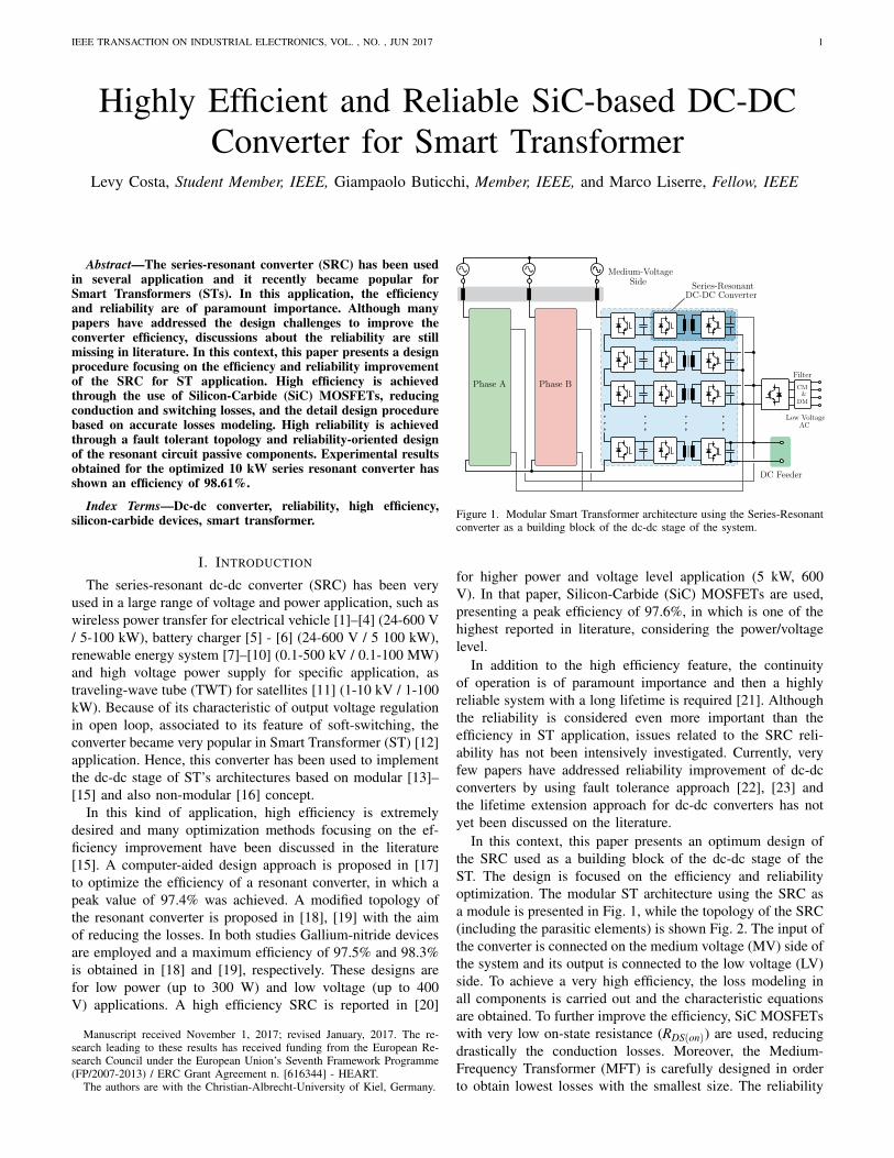
Figure 8. Graphic analysis of the SRC efficiency (a) and resonant capacitorlifetime (reliability) (b) in terms of the Lr and Cr .
VCpk(Cr) =Ii
8 fsCr
(10)
iL(rms)(Lr,Cr) = iLpk ·
√
γ
2= iLpk ·
√
1
2 · fs
√LrCr
(11)
L(V,T )∼ L(iL(rms), iL(os),VCpk)∼ L(Lr,Cr) (12)
C. Tank Circuit Parameter Selection
Analyzing the efficiency curve and lifetime capacitors pre-
sented in 8, it is noticed that the efficiency reaches its maxi-
mum value when fo = fs, as expected and already discussed.
In the graphic 8 (b), the capacitor lifetime is longer for lower
values of Lr and higher values of Cr. Therefore, to extended as
much as possible the capacitor lifetime, the inductance Lr must
be as smaller as possible, while the capacitance Cr should be as
big as possible, keeping fo constant. The minimum inductance
value possible is constrained by the leakage inductance of
the transformer. Therefore, only the leakage inductance of
the transformer should be used and no external inductance
is added.
V. PROTOTYPE IMPLEMENTATION AND EXPERIMENTAL
RESULTS
In order to evaluate the converter performance experimen-
tally and verify the presented design procedure, a prototype
was built and tested. The main specifications are shown in Ta-
ble I. The transformer implementation, converter construction
and the final results are discussed.
A. Medium-Frequency Transformer Implementation and Tests
The MFT was implemented according to the design pre-
sented in Section III. As a result of the design, 2 cores
E65/32/27 from EPCOS/TDK were used in parallel and the
physical implementation is described in Table IV. The im-
plemented transformer was experimentally evaluated and its
main parameters, as well as the core losses and wire losses
were obtained. The intrinsic parameters of the transformer are
shown in Table VI.
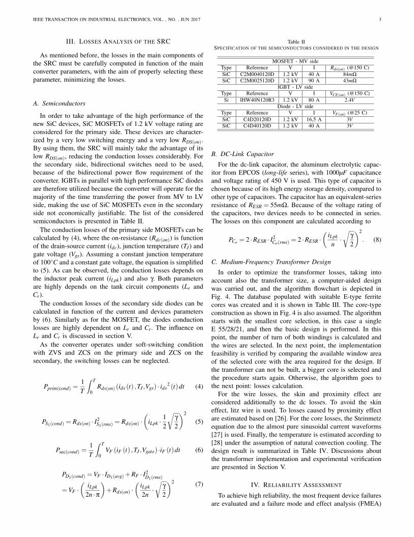
Table VIMEASURED PARAMETERS OF THE MFT
Leakage inductance Lleak = 13.5µH
Winding resistance (primary and secondary) Rwire = 86mΩ
Magnetizing inductance Lm = 7.93mH
Core Losses Rcore = 309.5kΩ
Total Losses PMFT = 56.4W
Figure 9. Temperature obtained during the open-circuit and short-circuit teston the transformer: (a) core losses (open-circuit test) and (a) wire losses (shot-circuit)
In order to evaluate more carefully the power dissipated on
the transformer, the open-circuit and short-circuit tests were
performed according to [32]. From these tests, it is possible
to separate the core losses from the wire losses, and to obtain
the wire losses decomposition in ac and dc losses. The total
losses of the MFT are presented in Table VI, while the losses
distribution is depicted in Fig. 14. As can be observed, the
wires are responsible for most of the losses (61%), where 22%
of this value are the ac losses, due to the proximity effect.
The expected ac losses is between 20% and 30% of the total
wire losses. Thus, the obtained value is in accordance to the
analysis, showing a good implementation of the transformer.
Finally, the temperature were measured in both tests, in
order to check the temperature rise due to the core and wire
losses individually. The results are presented in Fig. 9 and it
is observed that the temperature is well below the maximum
of 100C.
B. Final Prototype Assembly
Once the resonant frequency and the transformer leakage
inductance are chosen, the resonant capacitance (Cr) can be
selected. As discussed in section IV, the resonant induc-
tance should be the transformer leakage inductance, then
Lr = 13.5µH. To select the resonant frequency, the dead-time
between the semiconductors of the same leg should be taken
into account. Moreover, a resonance frequency slight above the
switching should be selected, so that the inductor current can
have a small zero-time, allowing the semiconductors to deplete
their stored charge. Therefore, assuming a dead-time of 1µs,
the resonance frequency of fo = 21.7kHz is select. To obtain
this value, the resonant capacitance should be Cr = 4.3µF .
Thus, the Cr is implemented by using 9 capacitors of 330nF
and 2 capacitors of 680nF connected in parallel.
For the semiconductor selection, those devices that pro-
vide the minimum conduction losses are selected, since the
IEEE TRANSACTION ON INDUSTRIAL ELECTRONICS, VOL. , NO. , JUN 2017 7
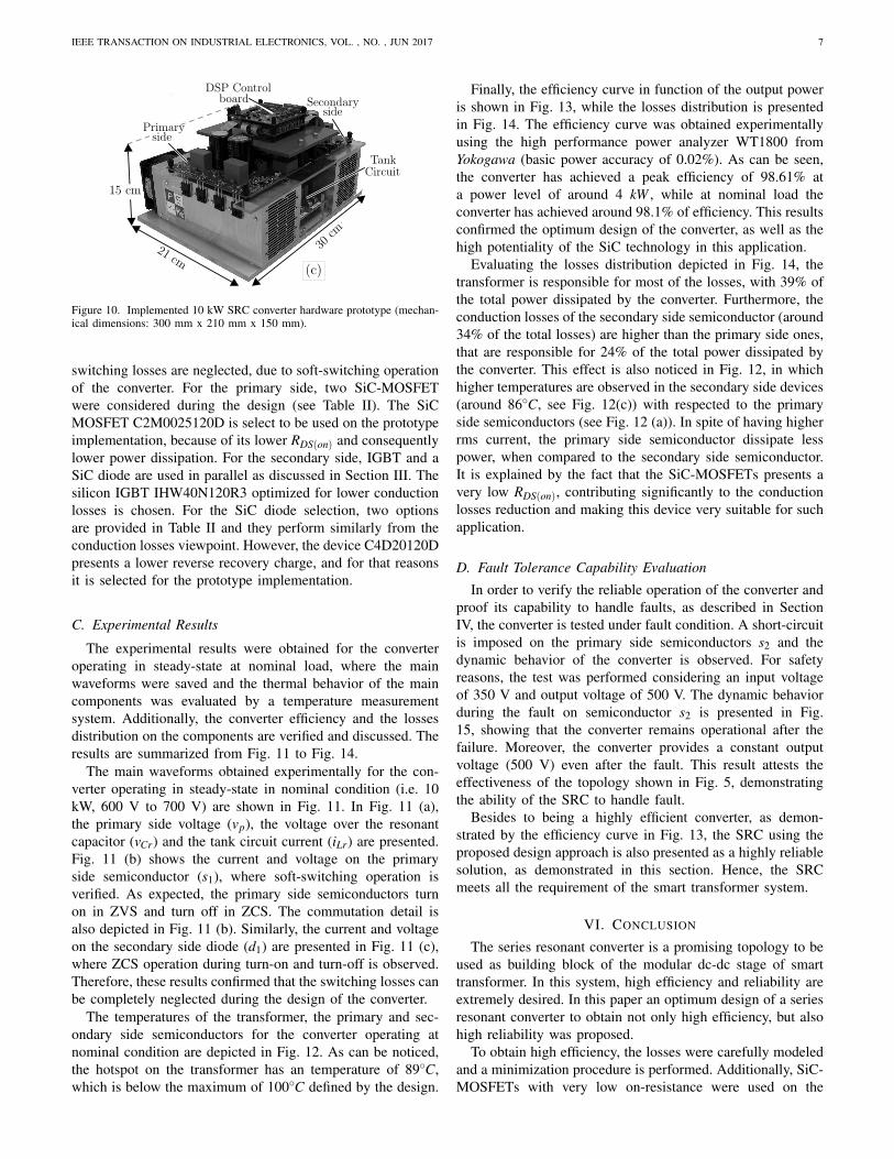
Figure 10. Implemented 10 kW SRC converter hardware prototype (mechan-ical dimensions: 300 mm x 210 mm x 150 mm).
switching losses are neglected, due to soft-switching operation
of the converter. For the primary side, two SiC-MOSFET
were considered during the design (see Table II). The SiC
MOSFET C2M0025120D is select to be used on the prototype
implementation, because of its lower RDS(on) and consequently
lower power dissipation. For the secondary side, IGBT and a
SiC diode are used in parallel as discussed in Section III. The
silicon IGBT IHW40N120R3 optimized for lower conduction
losses is chosen. For the SiC diode selection, two options
are provided in Table II and they perform similarly from the
conduction losses viewpoint. However, the device C4D20120D
presents a lower reverse recovery charge, and for that reasons
it is selected for the prototype implementation.
C. Experimental Results
The experimental results were obtained for the converter
operating in steady-state at nominal load, where the main
waveforms were saved and the thermal behavior of the main
components was evaluated by a temperature measurement
system. Additionally, the converter efficiency and the losses
distribution on the components are verified and discussed. The
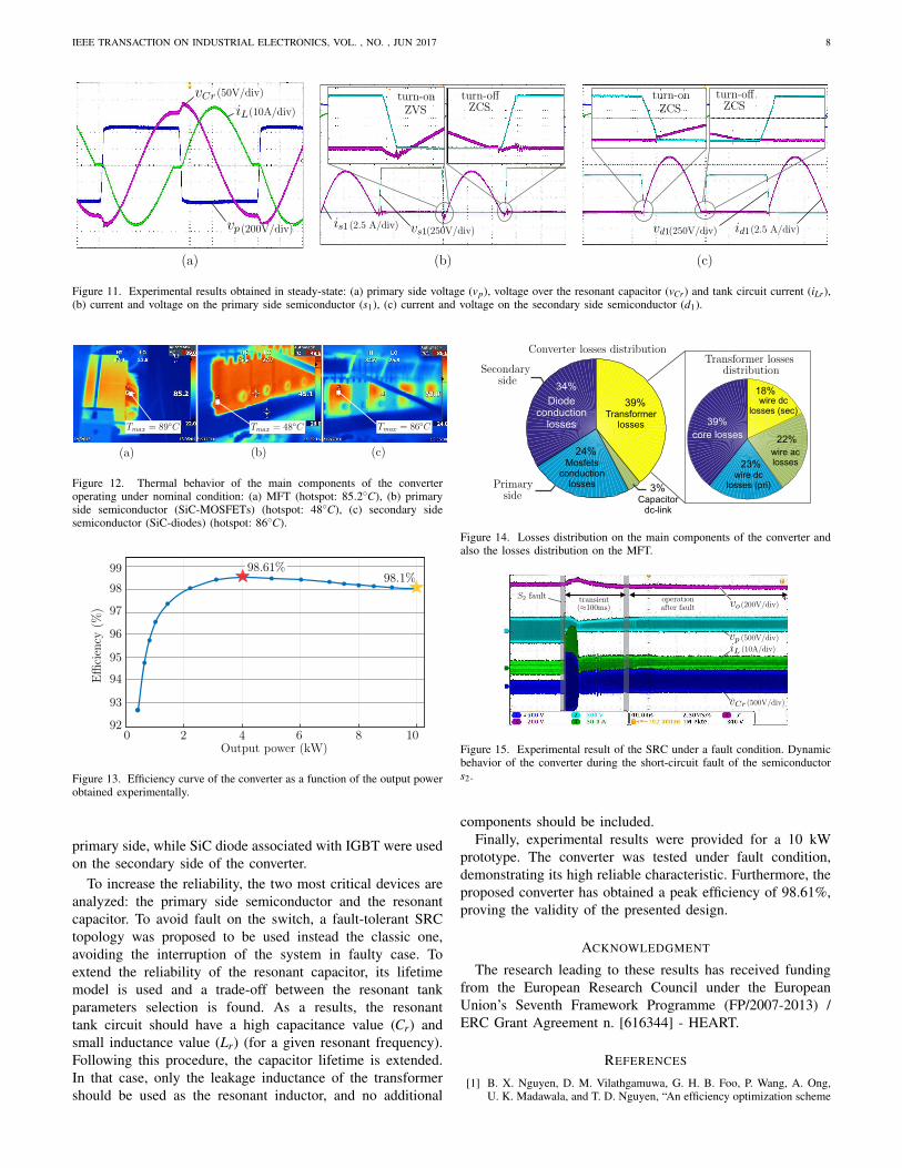
results are summarized from Fig. 11 to Fig. 14.
The main waveforms obtained experimentally for the con-
verter operating in steady-state in nominal condition (i.e. 10
kW, 600 V to 700 V) are shown in Fig. 11. In Fig. 11 (a),
the primary side voltage (vp), the voltage over the resonant
capacitor (vCr) and the tank circuit current (iLr) are presented.
Fig. 11 (b) shows the current and voltage on the primary
side semiconductor (s1), where soft-switching operation is
verified. As expected, the primary side semiconductors turn
on in ZVS and turn off in ZCS. The commutation detail is
also depicted in Fig. 11 (b). Similarly, the current and voltage
on the secondary side diode (d1) are presented in Fig. 11 (c),
where ZCS operation during turn-on and turn-off is observed.
Therefore, these results confirmed that the switching losses can
be completely neglected during the design of the converter.
The temperatures of the transformer, the primary and sec-
ondary side semiconductors for the converter operating at
nominal condition are depicted in Fig. 12. As can be noticed,
the hotspot on the transformer has an temperature of 89C,
which is below the maximum of 100C defined by the design.
Finally, the efficiency curve in function of the output power
is shown in Fig. 13, while the losses distribution is presented
in Fig. 14. The efficiency curve was obtained experimentally
using the high performance power analyzer WT1800 from
Yokogawa (basic power accuracy of 0.02%). As can be seen,
the converter has achieved a peak efficiency of 98.61% at
a power level of around 4 kW , while at nominal load the
converter has achieved around 98.1% of efficiency. This results
confirmed the optimum design of the converter, as well as the
high potentiality of the SiC technology in this application.
Evaluating the losses distribution depicted in Fig. 14, the
transformer is responsible for most of the losses, with 39% of
the total power dissipated by the converter. Furthermore, the
conduction losses of the secondary side semiconductor (around
34% of the total losses) are higher than the primary side ones,
that are responsible for 24% of the total power dissipated by
the converter. This effect is also noticed in Fig. 12, in which
higher temperatures are observed in the secondary side devices
(around 86C, see Fig. 12(c)) with respected to the primary
side semiconductors (see Fig. 12 (a)). In spite of having higher
rms current, the primary side semiconductor dissipate less
power, when compared to the secondary side semiconductor.
It is explained by the fact that the SiC-MOSFETs presents a
very low RDS(on), contributing significantly to the conduction
losses reduction and making this device very suitable for such
application.
D. Fault Tolerance Capability Evaluation
In order to verify the reliable operation of the converter and
proof its capability to handle faults, as described in Section
IV, the converter is tested under fault condition. A short-circuit
is imposed on the primary side semiconductors s2 and the
dynamic behavior of the converter is observed. For safety
reasons, the test was performed considering an input voltage
of 350 V and output voltage of 500 V. The dynamic behavior
during the fault on semiconductor s2 is presented in Fig.
15, showing that the converter remains operational after the
failure. Moreover, the converter provides a constant output
voltage (500 V) even after the fault. This result attests the
effectiveness of the topology shown in Fig. 5, demonstrating
the ability of the SRC to handle fault.
Besides to being a highly efficient converter, as demon-
strated by the efficiency curve in Fig. 13, the SRC using the
proposed design approach is also presented as a highly reliable
solution, as demonstrated in this section. Hence, the SRC
meets all the requirement of the smart transformer system.
VI. CONCLUSION
The series resonant converter is a promising topology to be
used as building block of the modular dc-dc stage of smart
transformer. In this system, high efficiency and reliability are
extremely desired. In this paper an optimum design of a series
resonant converter to obtain not only high efficiency, but also
high reliability was proposed.
To obtain high efficiency, the losses were carefully modeled
and a minimization procedure is performed. Additionally, SiC-
MOSFETs with very low on-resistance were used on the
IEEE TRANSACTION ON INDUSTRIAL ELECTRONICS, VOL. , NO. , JUN 2017 8
Figure 11. Experimental results obtained in steady-state: (a) primary side voltage (vp), voltage over the resonant capacitor (vCr) and tank circuit current (iLr),(b) current and voltage on the primary side semiconductor (s1), (c) current and voltage on the secondary side semiconductor (d1).
Figure 12. Thermal behavior of the main components of the converteroperating under nominal condition: (a) MFT (hotspot: 85.2C), (b) primaryside semiconductor (SiC-MOSFETs) (hotspot: 48C), (c) secondary sidesemiconductor (SiC-diodes) (hotspot: 86C).
Figure 13. Efficiency curve of the converter as a function of the output powerobtained experimentally.
primary side, while SiC diode associated with IGBT were used
on the secondary side of the converter.
To increase the reliability, the two most critical devices are
analyzed: the primary side semiconductor and the resonant
capacitor. To avoid fault on the switch, a fault-tolerant SRC
topology was proposed to be used instead the classic one,
avoiding the interruption of the system in faulty case. To
extend the reliability of the resonant capacitor, its lifetime
model is used and a trade-off between the resonant tank
parameters selection is found. As a results, the resonant
tank circuit should have a high capacitance value (Cr) and
small inductance value (Lr) (for a given resonant frequency).
Following this procedure, the capacitor lifetime is extended.
In that case, only the leakage inductance of the transformer
should be used as the resonant inductor, and no additional
39%
34%
core losses
Diodeconduction
losses
18%
39%
22%
23%
24%
3%
wire dclosses (sec)Transformer
losses
wire dclosses (pri)
Mosfetsconduction
losses
Capacitordc-link
wire aclosses
Figure 14. Losses distribution on the main components of the converter andalso the losses distribution on the MFT.
Figure 15. Experimental result of the SRC under a fault condition. Dynamicbehavior of the converter during the short-circuit fault of the semiconductors2.
components should be included.
Finally, experimental results were provided for a 10 kW
prototype. The converter was tested under fault condition,
demonstrating its high reliable characteristic. Furthermore, the
proposed converter has obtained a peak efficiency of 98.61%,
proving the validity of the presented design.
ACKNOWLEDGMENT
The research leading to these results has received funding
from the European Research Council under the European
Union’s Seventh Framework Programme (FP/2007-2013) /
ERC Grant Agreement n. [616344] - HEART.
REFERENCES
[1] B. X. Nguyen, D. M. Vilathgamuwa, G. H. B. Foo, P. Wang, A. Ong,U. K. Madawala, and T. D. Nguyen, “An efficiency optimization scheme

IEEE TRANSACTION ON INDUSTRIAL ELECTRONICS, VOL. , NO. , JUN 2017 9
for bidirectional inductive power transfer systems,” IEEE Transactions
on Power Electronics, vol. 30, no. 11, pp. 6310–6319, Nov 2015.[2] A. Berger, M. Agostinelli, S. Vesti, J. A. Oliver, J. A. Cobos, and
M. Huemer, “A wireless charging system applying phase-shift andamplitude control to maximize efficiency and extractable power,” IEEE
Transactions on Power Electronics, vol. 30, no. 11, pp. 6338–6348, Nov2015.
[3] M. Petersen and F. Fuchs, “Load dependent power control in series-series compensated electric vehicle inductive power transfer systems,”in European Conference on Power Electronics and Applications (EPE-
ECCE Europe), Aug 2014, pp. 1–10.[4] N. Liu and T. G. Habetler, “Design of a universal inductive charger
for multiple electric vehicle models,” IEEE Transactions on Power
Electronics, vol. 30, no. 11, pp. 6378–6390, Nov 2015.[5] I. O. Lee, “Hybrid pwm-resonant converter for electric vehicle on-board
battery chargers,” IEEE Transactions on Power Electronics, vol. 31,no. 5, pp. 3639–3649, May 2016.
[6] N. Shafiei, M. Ordonez, M. Craciun, C. Botting, and M. Edington, “Burstmode elimination in high-power llc resonant battery charger for electricvehicles,” IEEE Transactions on Power Electronics, vol. 31, no. 2, pp.1173–1188, Feb 2016.
[7] D. Jovcic and B. Ooi, “High-power, resonant dc/dc converter forintegration of renewable sources,” in IEEE Bucharest PowerTech, June2009, pp. 1–6.
[8] D. Jovcic and L. Zhang, “Lcl dc/dc converter for dc grids,” IEEE
Transactions on Power Delivery, vol. 28, no. 4, pp. 2071–2079, Oct2013.
[9] X. Sun, Y. Shen, Y. Zhu, and X. Guo, “Interleaved boost-integrated llcresonant converter with fixed-frequency pwm control for renewable en-ergy generation applications,” IEEE Transactions on Power Electronics,vol. 30, no. 8, pp. 4312–4326, Aug 2015.
[10] C. Meyer and R. De Doncker, “Design of a three-phase series resonantconverter for offshore dc grids,” in 42nd IAS Annual Meeting. Confer-
ence Record of the 2007 IEEE Industry Applications Conference, Sept2007, pp. 216–223.
[11] T. Lazzarin, O. Custodio, C. C. Motta, and I. Barbi, “An isolateddc-dc converter with high-output-voltage for a twta,” in International
Telecommunications Energy Conference (INTELEC), Sept 2014, pp. 1–7.
[12] M. Liserre, G. Buticchi, M. Andresen, G. D. Carne, L. F. Costa, andZ. X. Zou, “The smart transformer: Impact on the electric grid andtechnology challenges,” IEEE Industrial Electronics Magazine, vol. 10,no. 2, pp. 46–58, Summer 2016.
[13] D. Dujic, G. Steinke, E. Bianda, S. Lewdeni-Schmid, C. Zhao, andJ. Steinke, “Characterization of a 6.5kv igbt for medium-voltage high-power resonant dc-dc converter,” in Applied Power Electronics Confer-
ence and Exposition (APEC), March 2013, pp. 1438–1444.[14] C. Zhao, D. Dujic, A. Mester, J. Steinke, M. Weiss, S. Lewdeni-
Schmid, T. Chaudhuri, and P. Stefanutti, “Power electronic tractiontransformer:medium voltage prototype,” IEEE Transactions on Indus-
trial Electronics, vol. 61, no. 7, pp. 3257–3268, July 2014.[15] J. E. Huber and J. W. Kolar, “Analysis and design of fixed voltage
transfer ratio dc/dc converter cells for phase-modular solid-state trans-formers,” in 2015 IEEE Energy Conversion Congress and Exposition
(ECCE), Sept 2015, pp. 5021–5029.[16] J. Wang, A. Q. Huang, W. Sung, Y. Liu, and B. J. Baliga, “Smart grid
technologies,” IEEE Industrial Electronics Magazine, vol. 3, no. 2, pp.16–23, June 2009.
[17] R. Yu, G. K. Y. Ho, B. M. H. Pong, B. W. K. Ling, and J. Lam,“Computer-aided design and optimization of high-efficiency llc seriesresonant converter,” IEEE Transactions on Power Electronics, vol. 27,no. 7, pp. 3243–3256, July 2012.
[18] T. LaBella, W. Yu, J. S. . Lai, M. Senesky, and D. Anderson, “Abidirectional-switch-based wide-input range high-efficiency isolated res-onant converter for photovoltaic applications,” IEEE Transactions on
Power Electronics, vol. 29, no. 7, pp. 3473–3484, July 2014.[19] T. LaBella and J. S. Lai, “A hybrid resonant converter utilizing a
bidirectional gan ac switch for high-efficiency pv applications,” IEEE
Transactions on Industry Applications, vol. 50, no. 5, pp. 3468–3475,Sept 2014.
[20] Y. Nakakohara, H. Otake, T. M. Evans, T. Yoshida, M. Tsuruya, andK. Nakahara, “Three-phase llc series resonant dc/dc converter usingsic mosfets to realize high-voltage and high-frequency operation,” IEEE
Transactions on Industrial Electronics, vol. 63, no. 4, pp. 2103–2110,April 2016.
[21] M. Liserre, M. Andresen, L. Costa, and G. Buticchi, “Power routingin modular smart transformers: Active thermal control through uneven
loading of cells,” IEEE Industrial Electronics Magazine, vol. 10, no. 3,pp. 43–53, Fall 2016.
[22] L. Costa, G. Buticchi, and M. Liserre, “A fault-tolerant series-resonantdc-dc converter,” IEEE Transactions on Power Electronics, vol. 32, no. 2,pp. 900–905, Feb 2017.
[23] E. Ribeiro, A. Cardoso, and C. Boccaletti, “Fault-tolerant strategy for aphotovoltaic dc-dc converter,” IEEE Transactions on Power Electronics,vol. 28, no. 6, pp. 3008–3018, June 2013.
[24] K. Afridi, “Resonant and soft-switching techniques in power elec-tronics,” Department of Electrical, Computer and Energy, ColoradoUniversity, Colorado, USA, Lectures Note, 2014.
[25] H. Wu, T. Mu, X. Gao, and Y. Xing, “A secondary-side phase-shift-controlled llc resonant converter with reduced conduction loss at normaloperation for hold-up time compensation application,” IEEE Transac-
tions on Power Electronics, vol. 30, no. 10, pp. 5352–5357, Oct 2015.[26] W. G. Hurley, E. Gath, and J. G. Breslin, “Optimizing the ac resistance
of multilayer transformer windings with arbitrary current waveforms,”IEEE Transactions on Power Electronics, vol. 15, no. 2, pp. 369–376,Mar 2000.
[27] K. Venkatachalam, C. R. Sullivan, T. Abdallah, and H. Tacca, “Accurateprediction of ferrite core loss with nonsinusoidal waveforms usingonly steinmetz parameters,” in Computers in Power Electronics, 2002.
Proceedings. 2002 IEEE Workshop on, June 2002, pp. 36–41.[28] M. K. Kazimierczuk, High-Frequency Magnetic Components. Wiley
Publishing, 2009.[29] “Power technology roadmap: Trends 2012-2017,” Power Sources Man-
ufacturers Association, USA, Report, 2013.[30] W. s. Choi, S. m. Young, and D. w. Kim, “Analysis of mosfet failure
modes in llc resonant converter,” in INTELEC 2009 - 31st International
Telecommunications Energy Conference, Oct 2009, pp. 1–6.[31] H. Wang and F. Blaabjerg, “Reliability of capacitors for dc-link applica-
tions in power electronic converters: An overview,” IEEE Transactions
on Industry Applications, vol. 50, no. 5, pp. 3569–3578, Sept 2014.[32] I. Villar, “Multiphysical characterization of medium-frequency power
electronic transformers,” Ph.D. dissertation, Swiss Federal Institute ofTechnology Lausanne, 2010.
Levy Ferreira Costa (S’14) received the B.S.degree in electrical engineering from the FederalUniversity of Ceara, Brazil, in 2010 and the M.S.degree from the Federal University of Santa Cata-rina, Brazil, in 2013. From 2013 to 2014, he was anElectrical Design Engineer with Schneider Electric,Brazil. He is currently working toward the Ph.D.degree at the Chair of Power Electronics, Christian-Albrechts-University of Kiel, Germany. His researchinterests include dc-dc converters, high-power con-verter systems and wide-bandgap semiconductors.
Giampaolo Buticchi (S’10-M’13) was born inParma, Italy, in 1985. He received the Masters de-gree in Electronic Engineering in 2009 and the Ph.Ddegree in Information Technologies in 2013 from theUniversity of Parma, Italy. He is now working asa postdoctoral research associate at the Universityof Kiel, Germany. His research area is focused onpower electronics for renewable energy systems,smart transformer fed micro-grids and reliability inpower electronics.

IEEE TRANSACTION ON INDUSTRIAL ELECTRONICS, VOL. , NO. , JUN 2017 10
Marco Liserre (S’00-M’02-SM’07-F’13) receivedthe M.Sc. and Ph.D degree in Electrical Engineeringfrom the Bari Polytechnic, respectively in 1998 and2002. He has been Associate Professor at Bari Poly-technic and Professor in reliable power electronicsat Aalborg University (Denmark). He is currentlyFull Professor and he holds the Chair of PowerElectronics at Christian-Albrechts-University of Kiel(Germany). He has published over 280 technicalpapers (more than 70 of them in international peer-reviewed journals), 4 chapters of a book and a book
(Grid Converters for Photovoltaic and Wind Power Systems, ISBN-10: 0-470-05751-3 IEEE-Wiley, second reprint, also translated in Chinese). Theseworks have received more than 16000 citations. Marco Liserre is listed inISI Thomson report The world’s most influential scientific minds from 2014.He has been awarded with an ERC Consolidator Grant for the project ’TheHighly Efficient And Reliable smart Transformer (HEART), a new Heartfor the Electric Distribution System. He is member of IAS, PELS, PESand IES. He is Associate Editor of the IEEE Transactions on Industrial
Electronics, IEEE Industrial Electronics Magazine, IEEE Transactions onIndustrial Informatics, where he is currently Co-Eic, IEEE Transactions onpower electronics and IEEE Journal of Emerging and Selected Topics in PowerElectronics. He has been Founder and Editor-in-Chief of the IEEE IndustrialElectronics Magazine, Founder and the Chairman of the Technical Committeeon Renewable Energy Systems, Co-Chairman of the International Symposiumon Industrial Electronics (ISIE 2010), IES Vice-President responsible of thepublications. He has received the IES 2009 Early Career Award, the IES2011 Anthony J. Hornfeck Service Award, the 2014 Dr. Bismal Bose EnergySystems Award, the 2011 Industrial Electronics Magazine best paper awardand the Third Prize paper award by the Industrial Power Converter Committeeat ECCE 2012, 2012. He is senior member of IES AdCom. In 2013 hehas been elevated to the IEEE fellow grade with the following citation “forcontributions to grid connection of renewable energy systems and industrialdrives”.
Recommended


