HCS201KEELOQ® Code Hopping Encoder
FEATURES
Security
• Programmable 28-bit serial number• Programmable 64-bit encryption key
• Each transmission is unique• 66-bit transmission code length• 32-bit hopping code
• 34-bit fixed code (28-bit serial number, 4-bit button code, 2-bit status)
• Encryption keys are read protected
Operating
• 3.5V-13V operation (2.0V min. using the Step up feature)
• Three button inputs• 7 functions available • Selectable baud rate
• Automatic code word completion• Battery low signal transmitted to receiver• Non-volatile synchronization data
Other
• Simple programming interface
• On-chip EEPROM• On-chip oscillator and timing components• Button inputs have internal pull-down resistors
• Minimum component count• Synchronous Transmission mode• Built-in step up regulator
Typical Applications
• The HCS201 is ideal for Remote Keyless Entry (RKE) applications. These applications include:
• Automotive RKE systems
• Automotive alarm systems• Automotive immobilizers• Gate and garage door openers
• Identity tokens• Burglar alarm systems
DESCRIPTION
The HCS201 from Microchip Technology Inc. is a codehopping encoder designed for secure Remote KeylessEntry (RKE) systems. The HCS201 utilizes the KEELOQ
code hopping technology, incorporating high security, asmall package outline and low cost. The HCS201 is aperfect solution for unidirectional remote keyless entrysystems and access control systems.
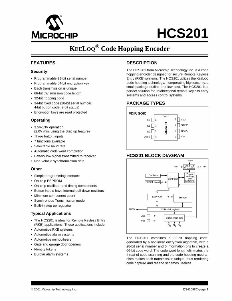
PACKAGE TYPES
HCS201 BLOCK DIAGRAM
The HCS201 combines a 32-bit hopping code,generated by a nonlinear encryption algorithm, with a28-bit serial number and 6 information bits to create a66-bit code word. The code word length eliminates thethreat of code scanning and the code hopping mecha-nism makes each transmission unique, thus renderingcode capture and resend schemes useless.
1
2
3
4
8
7
6
5
S0
S1
S2
VDDB
VDD
STEP
DATA
VSS
PDIP, SOIC
HC
S201
VSS
VDD
Oscillator
RESET circuitController
Powerlatching
andswitching
Button input port
32-bit shift register
EncoderEEPROM
DATA
S2 S1 S0
Step UpController
VDDB
VDD STEP
2001 Microchip Technology Inc. DS41098C-page 1
HCS201
The crypt key, serial number and configuration data arestored in an EEPROM array which is not accessible viaany external connection. The EEPROM data is pro-grammable but read-protected. The data can be veri-fied only after an automatic erase and programmingoperation. This protects against attempts to gainaccess to keys or manipulate synchronization values.The HCS201 provides an easy-to-use serial interfacefor programming the necessary keys, system parame-ters and configuration data.
1.0 SYSTEM OVERVIEW
Key Terms
The following is a list of key terms used throughout thisdata sheet. For additional information on KEELOQ andCode Hopping, refer to Technical Brief 3 (TB003).
• RKE - Remote Keyless Entry
• Button Status - Indicates what button input(s) activated the transmission. Encompasses the 4 button status bits S3, S2, S1 and S0 (Figure 4-2).
• Code Hopping - A method by which a code, viewed externally to the system, appears to change unpredictably each time it is transmitted.
• Code word - A block of data that is repeatedly transmitted upon button activation (Figure 4-1).
• Transmission - A data stream consisting of repeating code words (Figure 8-1).
• Crypt key - A unique and secret 64-bit number used to encrypt and decrypt data. In a symmetri-cal block cipher such as the KEELOQ algorithm, the encryption and decryption keys are equal and will therefore be referred to generally as the crypt key.
• Encoder - A device that generates and encodes data.
• Encryption Algorithm - A recipe whereby data is scrambled using a crypt key. The data can only be interpreted by the respective decryption algorithm using the same crypt key.
• Decoder - A device that decodes data received from an encoder.
• Decryption algorithm - A recipe whereby data scrambled by an encryption algorithm can be unscrambled using the same crypt key.
• Learn – Learning involves the receiver calculating the transmitter’s appropriate crypt key, decrypting the received hopping code and storing the serial number, synchronization counter value and crypt key in EEPROM. The KEELOQ product family facil-itates several learning strategies to be imple-mented on the decoder. The following are examples of what can be done. - Simple Learning
The receiver uses a fixed crypt key, common to all components of all systems by the same manufacturer, to decrypt the received code word’s encrypted portion.
- Normal LearningThe receiver uses information transmitted during normal operation to derive the crypt key and decrypt the received code word’s encrypted portion.
- Secure LearnThe transmitter is activated through a special button combination to transmit a stored 60-bit seed value used to generate the transmitter’s crypt key. The receiver uses this seed value to derive the same crypt key and decrypt the received code word’s encrypted portion.
• Manufacturer’s code – A unique and secret 64-bit number used to generate unique encoder crypt keys. Each encoder is programmed with a crypt key that is a function of the manufacturer’s code. Each decoder is programmed with the manufac-turer code itself.
The HCS201 code hopping encoder is designed specif-ically for keyless entry systems; primarily vehicles andhome garage door openers. The encoder portion of akeyless entry system is integrated into a transmitter,carried by the user and operated to gain access to avehicle or restricted area. The HCS201 is meant to bea cost-effective yet secure solution to such systems,requiring very few external components (Figure 2-1).
Most low-end keyless entry transmitters are given afixed identification code that is transmitted every time abutton is pushed. The number of unique identificationcodes in a low-end system is usually a relatively smallnumber. These shortcomings provide an opportunityfor a sophisticated thief to create a device that ‘grabs’a transmission and retransmits it later, or a device thatquickly ‘scans’ all possible identification codes until thecorrect one is found.
The HCS201, on the other hand, employs the KEELOQ
code hopping technology coupled with a transmissionlength of 66 bits to virtually eliminate the use of code‘grabbing’ or code ‘scanning’. The high security level ofthe HCS201 is based on the patented KEELOQ technol-ogy. A block cipher based on a block length of 32 bitsand a key length of 64 bits is used. The algorithmobscures the information in such a way that even if thetransmission information (before coding) differs by onlyone bit from that of the previous transmission, the next
DS41098C-page 2 2001 Microchip Technology Inc.
HCS201
coded transmission will be completely different. Statis-tically, if only one bit in the 32-bit string of informationchanges, greater than 50 percent of the coded trans-mission bits will change.
As indicated in the block diagram on page one, theHCS201 has a small EEPROM array which must beloaded with several parameters before use; most oftenprogrammed by the manufacturer at the time of produc-tion. The most important of these are:
• A 28-bit serial number, typically unique for every encoder
• A crypt key• An initial 16-bit synchronization value• A 16-bit configuration value
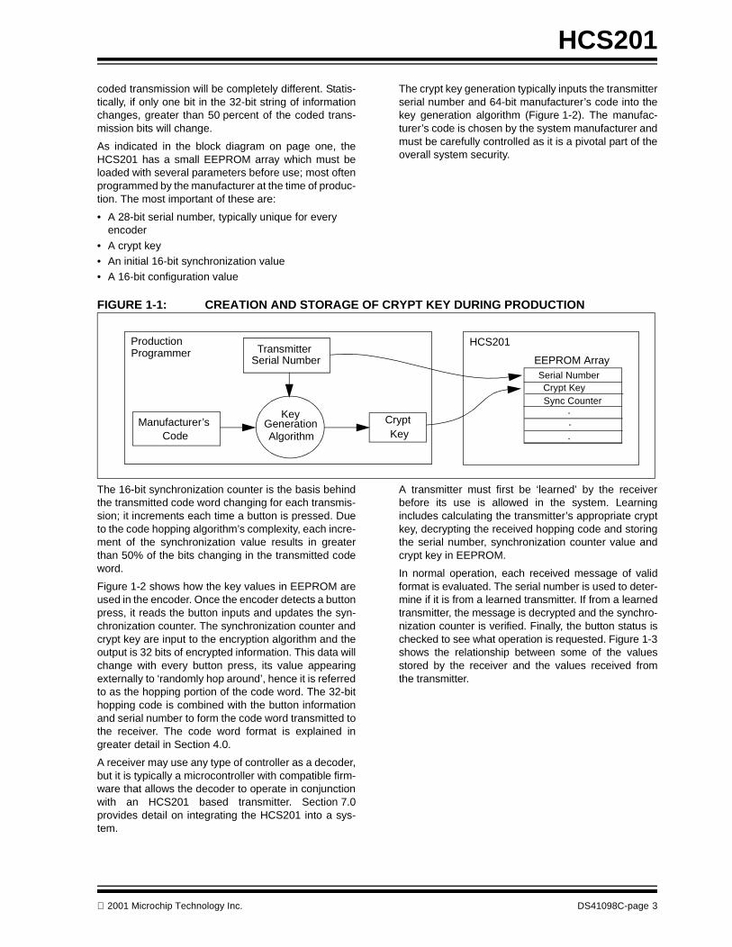
The crypt key generation typically inputs the transmitterserial number and 64-bit manufacturer’s code into thekey generation algorithm (Figure 1-2). The manufac-turer’s code is chosen by the system manufacturer andmust be carefully controlled as it is a pivotal part of theoverall system security.
FIGURE 1-1: CREATION AND STORAGE OF CRYPT KEY DURING PRODUCTION
The 16-bit synchronization counter is the basis behindthe transmitted code word changing for each transmis-sion; it increments each time a button is pressed. Dueto the code hopping algorithm’s complexity, each incre-ment of the synchronization value results in greaterthan 50% of the bits changing in the transmitted codeword.
Figure 1-2 shows how the key values in EEPROM areused in the encoder. Once the encoder detects a buttonpress, it reads the button inputs and updates the syn-chronization counter. The synchronization counter andcrypt key are input to the encryption algorithm and theoutput is 32 bits of encrypted information. This data willchange with every button press, its value appearingexternally to ‘randomly hop around’, hence it is referredto as the hopping portion of the code word. The 32-bithopping code is combined with the button informationand serial number to form the code word transmitted tothe receiver. The code word format is explained ingreater detail in Section 4.0.
A receiver may use any type of controller as a decoder,but it is typically a microcontroller with compatible firm-ware that allows the decoder to operate in conjunctionwith an HCS201 based transmitter. Section 7.0provides detail on integrating the HCS201 into a sys-tem.
A transmitter must first be ‘learned’ by the receiverbefore its use is allowed in the system. Learningincludes calculating the transmitter’s appropriate cryptkey, decrypting the received hopping code and storingthe serial number, synchronization counter value andcrypt key in EEPROM.
In normal operation, each received message of validformat is evaluated. The serial number is used to deter-mine if it is from a learned transmitter. If from a learnedtransmitter, the message is decrypted and the synchro-nization counter is verified. Finally, the button status ischecked to see what operation is requested. Figure 1-3shows the relationship between some of the valuesstored by the receiver and the values received fromthe transmitter.
Transmitter
Manufacturer’s
Serial Number
Code
Crypt Key
KeyGenerationAlgorithm
Serial NumberCrypt KeySync Counter
..
.
HCS201ProductionProgrammer
EEPROM Array
2001 Microchip Technology Inc. DS41098C-page 3

HCS201
FIGURE 1-2: BUILDING THE TRANSMITTED CODE WORD (ENCODER)
FIGURE 1-3: BASIC OPERATION OF RECEIVER (DECODER)
NOTE: Circled numbers indicate the order of execution.
Button PressInformation
EEPROM Array
32 Bits Encrypted DataSerial Number
Transmitted Information
Crypt Key
Sync Counter
Serial Number
KEELOQ
EncryptionAlgorithm
Button Press Information
EEPROM Array
Manufacturer Code 32 Bits of Encrypted DataSerial Number
Received Information
DecryptedSynchronization Counter
Check for Match
Sync Counter
Serial Number
KEELOQDecryptionAlgorithm
1
3
4
Check for Match2
Perform Function Indicated by button press 5
Crypt Key
DS41098C-page 4 2001 Microchip Technology Inc.
HCS201
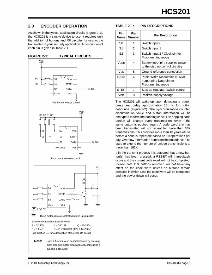
2.0 ENCODER OPERATION
As shown in the typical application circuits (Figure 2-1),the HCS201 is a simple device to use. It requires onlythe addition of buttons and RF circuitry for use as thetransmitter in your security application. A description ofeach pin is given in Table 2-1.
FIGURE 2-1: TYPICAL CIRCUITS
TABLE 2-1: PIN DESCRIPTIONS
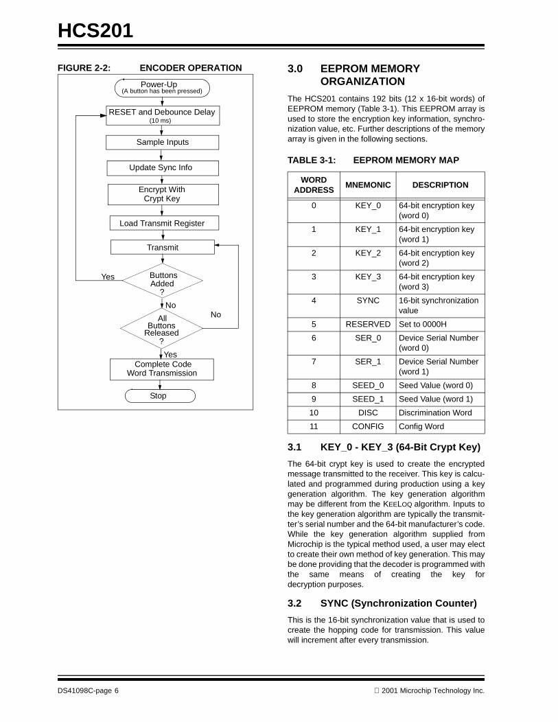
The HCS201 will wake-up upon detecting a buttonpress and delay approximately 10 ms for buttondebounce (Figure 2-2). The synchronization counter,discrimination value and button information will beencrypted to form the hopping code. The hopping codeportion will change every transmission, even if thesame button is pushed again. A code word that hasbeen transmitted will not repeat for more than 64Ktransmissions. This provides more than 18 years of usebefore a code is repeated; based on 10 operations perday. Overflow information sent from the encoder can beused to extend the number of unique transmissions tomore than 192K.
If in the transmit process it is detected that a new but-ton(s) has been pressed, a RESET will immediatelyoccur and the current code word will not be completed.Please note that buttons removed will not have anyeffect on the code word unless no buttons remainpressed; in which case the code word will be completedand the power-down will occur.
VDD
B0
Tx out
S0
S1
S2
VDDB
STEP
VDD
DATA
VSS
Two button remote control
B1
Tx out
S0
S1
S2
STEP
VDD
DATA
VSS
Four button remote control
B3 B2 B1 B0
Note: Up to 7 functions can be implemented by pressing
more than one button simultaneously or by using a
suitable diode array.
S0
S1
S2
STEP
VDD
DATA
VSSVDDB
VDDB
VDD
Tx out
Three button remote control with Step up regulator
VDD
2.0-6.0V
External components sample values:
R = 5.1 KΩ L = 390 uH Q = 2N3904
C = 1.0 uF D = ZHCS400CT (40V 0.4A Zetex)
(see Section 5.6 for a description of the Step Up circuit)
R
L
D
CQ
Pin Name
Pin Number
Pin Description
S0 1 Switch input 0
S1 2 Switch input 1
S2 3 Switch input 2 / Clock pin for Programming mode
VDDB 4 Battery input pin, supplies power to the step up control circuitry
VSS 5 Ground reference connection
DATA 6 Pulse Width Modulation (PWM)output pin / Data pin forProgramming mode
STEP 7 Step up regulator switch control
VDD 8 Positive supply voltage
2001 Microchip Technology Inc. DS41098C-page 5
HCS201
FIGURE 2-2: ENCODER OPERATION 3.0 EEPROM MEMORY ORGANIZATION
The HCS201 contains 192 bits (12 x 16-bit words) ofEEPROM memory (Table 3-1). This EEPROM array isused to store the encryption key information, synchro-nization value, etc. Further descriptions of the memoryarray is given in the following sections.
TABLE 3-1: EEPROM MEMORY MAP
3.1 KEY_0 - KEY_3 (64-Bit Crypt Key)
The 64-bit crypt key is used to create the encryptedmessage transmitted to the receiver. This key is calcu-lated and programmed during production using a keygeneration algorithm. The key generation algorithmmay be different from the KEELOQ algorithm. Inputs tothe key generation algorithm are typically the transmit-ter’s serial number and the 64-bit manufacturer’s code.While the key generation algorithm supplied fromMicrochip is the typical method used, a user may electto create their own method of key generation. This maybe done providing that the decoder is programmed withthe same means of creating the key fordecryption purposes.
3.2 SYNC (Synchronization Counter)
This is the 16-bit synchronization value that is used tocreate the hopping code for transmission. This valuewill increment after every transmission.
Power-Up
RESET and Debounce Delay (10 ms)
Sample Inputs
Update Sync Info
Encrypt With
Load Transmit Register
ButtonsAdded
?
AllButtons
Released?
(A button has been pressed)
Transmit
Stop
No
Yes
No
Yes
Crypt Key
Complete Code Word Transmission
WORD ADDRESS
MNEMONIC DESCRIPTION
0 KEY_0 64-bit encryption key(word 0)
1 KEY_1 64-bit encryption key(word 1)
2 KEY_2 64-bit encryption key(word 2)
3 KEY_3 64-bit encryption key(word 3)
4 SYNC 16-bit synchronizationvalue
5 RESERVED Set to 0000H
6 SER_0 Device Serial Number(word 0)
7 SER_1 Device Serial Number(word 1)
8 SEED_0 Seed Value (word 0)
9 SEED_1 Seed Value (word 1)
10 DISC Discrimination Word
11 CONFIG Config Word
DS41098C-page 6 2001 Microchip Technology Inc.

HCS201
3.3 Reserved
Must be initialized to 0000H.
3.4 SER_0, SER_1 (Encoder Serial Number)
SER_0 and SER_1 are the lower and upper words ofthe device serial number, respectively. Although thereare 32 bits allocated for the serial number, only thelower order 28 bits are transmitted. The serial numberis meant to be unique for every transmitter.
3.5 SEED_0, SEED_1 (Seed Word)
The 2-word (32-bit) seed code will be transmitted whenall three buttons are pressed at the same time (seeFigure 4-2). This allows the system designer to imple-ment the secure learn feature or use this fixed codeword as part of a different key generation/tracking pro-cess.
TABLE 3-2: DISCRIMINATION WORD
3.6 DISC(Discrimination Word)
The discrimination value aids the post-decryptioncheck on the decoder end. It may be any value, but ina typical system it will be programmed as the 12 LeastSignificant bits of the serial number. Values other thanthis must be separately stored by the receiver when atransmitter is learned. The discrimination bits are partof the information that form the encrypted portion ofthe transmission (Figure 4-2). After the receiver hasdecrypted a transmission, the discrimination bits arechecked against the receiver’s stored value to verifythat the decryption process was valid. If the discrimi-nation value was programmed as the 12 LSb’s of the
serial number then it may merely be compared to therespective bits of the received serial number; savingEEPROM space.
3.7 CONFIG (Configuration Word)
The Configuration Word is a 16-bit word stored inEEPROM array that is used by the device to store infor-mation used during the encryption process, as well asthe status of option configurations. Further explana-tions of each of the bits are described in the followingsections.
TABLE 3-3: CONFIGURATION WORD
3.7.1 OSCILLATOR TUNING BITS (OSC0 AND OSC3)
These bits are used to tune the frequency of theHCS201 internal clock oscillator to within ±10% of itsnominal value over temperature and voltage.
3.7.2 LOW VOLTAGE TRIP POINT SELECT (VLOWS)
The low voltage trip point select bit (VLOWS) and the S3setting bit (S3SET) are used to determine when to sendthe VLOW signal to the receiver.
* See also Section 3.7.6
Bit Number Bit Description
0 Discrimination Bit 01 Discrimination Bit 12 Discrimination Bit 23 Discrimination Bit 34 Discrimination Bit 45 Discrimination Bit 56 Discrimination Bit 67 Discrimination Bit 78 Discrimination Bit 89 Discrimination Bit 910 Discrimination Bit 1011 Discrimination Bit 1112 Not Used13 Not Used14 Not Used15 Not Used
Bit Number Bit Name
0 OSC01 OSC12 OSC23 OSC34 VLOWS
5 BRS6 MTX47 TXEN8 S3SET9 XSER
10 Not Used11 Not Used12 Not Used13 Not Used14 Not Used15 Not Used
TABLE 3-4: TRIP POINT SELECT
VLOWS S3SET* Trip Point
0 0 4.40 1 4.4
1 0 91 1 6.75
2001 Microchip Technology Inc. DS41098C-page 7
HCS201
3.7.3 BAUD RATE SELECT BITS (BRS)
BRS selects the speed of transmission and the codeword blanking. Table 3-5 shows how the bit is used toselect the different baud rates and Section 5.5 providesdetailed explanation in code word blanking.
TABLE 3-5: BAUDRATE SELECT
3.7.4 MINIMUM FOUR TRANSMISSIONS (MTX4)
If this bit is cleared, only one code is completed if theHCS201 is activated. If this bit is set, at least four com-plete code words are transmitted, even if code wordblanking is enabled.
3.7.5 TRANSMIT PULSE ENABLE (TXEN)
If this bit is cleared, no transmission pulse is transmit-ted before a transmission. If the bit is set, a STARTpulse (1 TE long) is transmitted after button de-bounc-ing, before the preamble of the first code word.
3.7.6 S3 SETTING (S3SET)
This bit determines the value of S3 in the function codeduring a transmission and the high trip point selectedby VLOWS in section 3.6.2. If this bit is cleared, S3 mir-rors S2 during a transmission. If the S3SET bit is set,S3 in the function code (Button Status) is always set,independent of the value of S2.
3.7.7 EXTENDED SERIAL NUMBER (XSER)
If this bit is set, a long 32-bit Serial Number is transmit-ted. If this bit is cleared, a standard 28-bit Serial Numberis transmitted followed by 4 bits of the function code(Button Status).
BRSBasic Pulse
ElementCode Words Transmitted
0 400 µs All
1 200 µs 1 out of 2
DS41098C-page 8 2001 Microchip Technology Inc.
HCS201
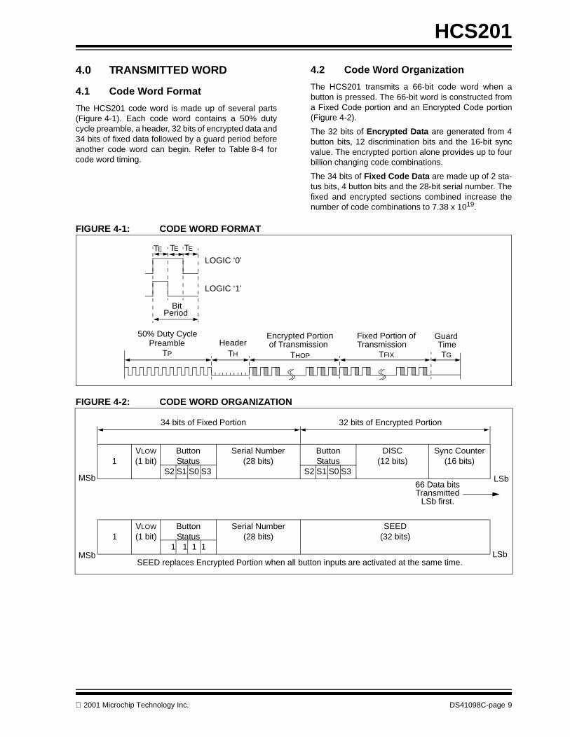
4.0 TRANSMITTED WORD
4.1 Code Word Format
The HCS201 code word is made up of several parts(Figure 4-1). Each code word contains a 50% dutycycle preamble, a header, 32 bits of encrypted data and34 bits of fixed data followed by a guard period beforeanother code word can begin. Refer to Table 8-4 forcode word timing.
4.2 Code Word Organization
The HCS201 transmits a 66-bit code word when abutton is pressed. The 66-bit word is constructed froma Fixed Code portion and an Encrypted Code portion(Figure 4-2).
The 32 bits of Encrypted Data are generated from 4button bits, 12 discrimination bits and the 16-bit syncvalue. The encrypted portion alone provides up to fourbillion changing code combinations.
The 34 bits of Fixed Code Data are made up of 2 sta-tus bits, 4 button bits and the 28-bit serial number. Thefixed and encrypted sections combined increase thenumber of code combinations to 7.38 x 10¹⁹.
FIGURE 4-1: CODE WORD FORMAT
FIGURE 4-2: CODE WORD ORGANIZATION
LOGIC ‘0’
LOGIC ‘1’
BitPeriod
Preamble HeaderEncrypted Portion of Transmission
Fixed Portion ofTransmission
Guard Time
TP TH THOP TFIX TG
TETETE
50% Duty Cycle
1VLOW
(1 bit)Button Status
S2 S1 S0 S3
Serial Number(28 bits)
Button Status
S2 S1 S0 S3
DISC(12 bits)
Sync Counter(16 bits)
1VLOW
(1 bit)Button Status
1 1 1 1
Serial Number(28 bits)
SEED(32 bits)
34 bits of Fixed Portion 32 bits of Encrypted Portion
66 Data bitsTransmitted
LSb first.
LSbMSb
MSb LSbSEED replaces Encrypted Portion when all button inputs are activated at the same time.
2001 Microchip Technology Inc. DS41098C-page 9

HCS201
4.3 Synchronous Transmission Mode
Synchronous Transmission mode can be used to clockthe code word out using an external clock.
To enter Synchronous Transmission mode, the Pro-gramming mode start-up sequence must be executedas shown in Figure 4-3. If either S1 or S0 is set on thefalling edge of S2 (or S3), the device enters Synchro-nous Transmission mode. In this mode, it functions asa normal transmitter, with the exception that the timingof the PWM data string is controlled externally and 16extra bits are transmitted at the end with the code word.
The button code will be the S0, S1 value at the fallingedge of S2 or S3. The timing of the PWM data string iscontrolled by supplying a clock on S2 or S3 and shouldnot exceed 20 kHz. The code word is the same as inPWM mode with 16 reserved bits at the end of theword. The reserved bits can be ignored. When in Syn-chronous Transmission mode S2 or S3 should not betoggled until all internal processing has been com-pleted as shown in Figure 4-4.
FIGURE 4-3: SYNCHRONOUS TRANSMISSION MODE (TXEN=0)
FIGURE 4-4: CODE WORD ORGANIZATION (SYNCHRONOUS TRANSMISSION MODE)
“01,10,11”
PWM
S2
S[1:0]
TPS TPH1 TPH2 t = 50ms Preamble Header Data
Reserved(16 bits)
Padding(2 bits)
Button Status
S2 S1 S0 S3
Serial Number(28 bits)
Button Status
S2 S1 S0 S3
DISC(12 bits)
Sync Counter(16 bits)
82 Data bitsTransmitted
LSb first.
LSbMSb
Fixed Portion Encrypted Portion
DS41098C-page 10 2001 Microchip Technology Inc.
HCS201
5.0 SPECIAL FEATURES
5.1 Code Word Completion
The code word completion feature ensures that entirecode words are transmitted, even if the button isreleased before the code word is complete. If the but-ton is held down beyond the time for one code word,multiple code words will result. If another button is acti-vated during a transmission, the active transmissionwill be aborted and a new transmission will begin usingthe new button information.
5.2 VLOW: Voltage LOW Indicator
The VLOW bit is transmitted with every transmission(Figure 8-4) and will be transmitted as a one if theoperating voltage has dropped below the low voltage trippoint. The trip point is selectable based on the batteryvoltage being used. See Section 3.7.2 for a descriptionof how the low voltage select option is set. This VLOW
signal is transmitted so the receiver can give an audiblesignal to the user that the transmitter battery is low.
5.3 Auto-Shutoff
The auto-shutoff function automatically stops the devicefrom transmitting if a button inadvertently gets pressedfor a long period of time. This will prevent the device fromdraining the battery if a button gets pressed while thetransmitter is in a pocket or purse. Time-out period is TTO.
5.4 Seed Transmission
In order to increase the level of security in a system, itis possible for the receiver to implement what is knownas a secure learn function. This can be done by utilizingthe seed value stored in EEPROM, transmitted onlywhen all three button inputs are pressed at the sametime (Table 5-1). Instead of the normal key generationinputs being used to create the crypt key, this seedvalue is used.
TABLE 5-1: PIN ACTIVATION TABLE
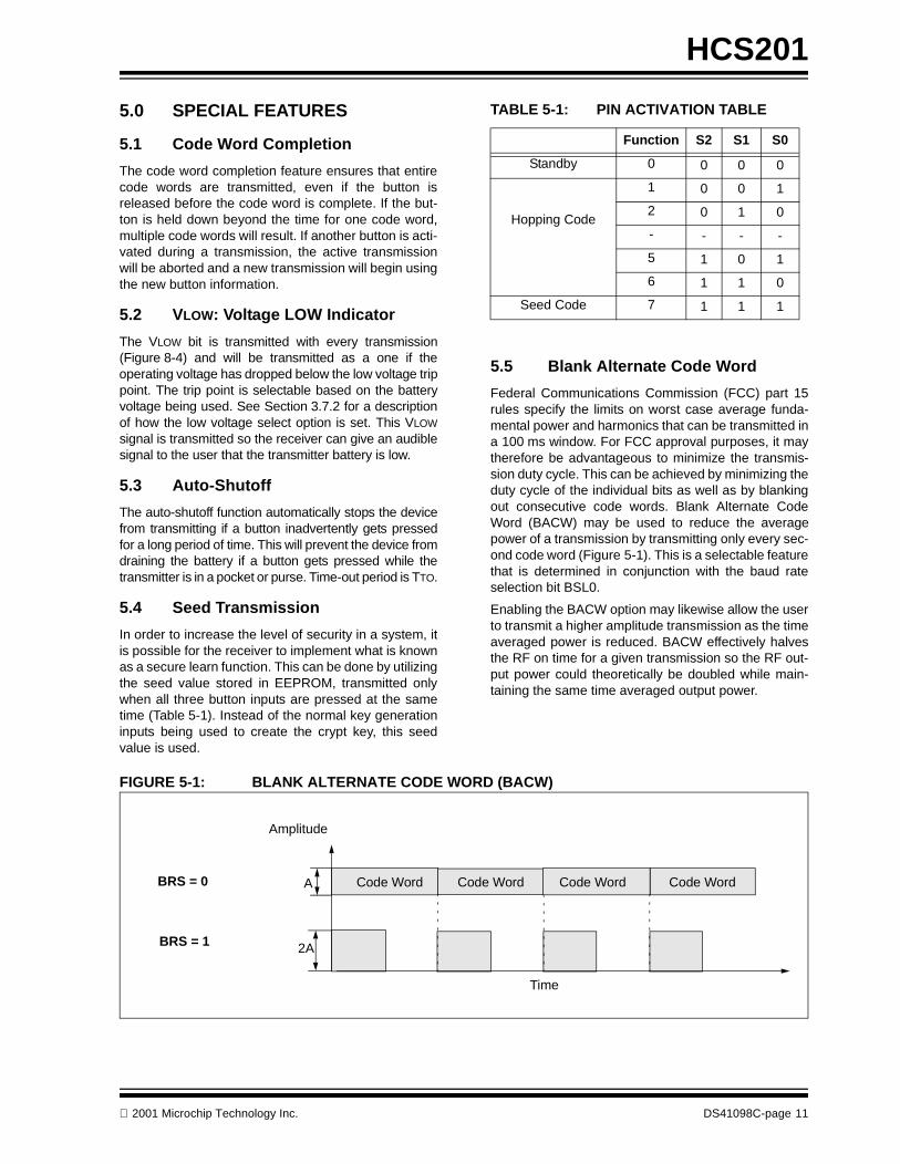
5.5 Blank Alternate Code Word
Federal Communications Commission (FCC) part 15rules specify the limits on worst case average funda-mental power and harmonics that can be transmitted ina 100 ms window. For FCC approval purposes, it maytherefore be advantageous to minimize the transmis-sion duty cycle. This can be achieved by minimizing theduty cycle of the individual bits as well as by blankingout consecutive code words. Blank Alternate CodeWord (BACW) may be used to reduce the averagepower of a transmission by transmitting only every sec-ond code word (Figure 5-1). This is a selectable featurethat is determined in conjunction with the baud rateselection bit BSL0.
Enabling the BACW option may likewise allow the userto transmit a higher amplitude transmission as the timeaveraged power is reduced. BACW effectively halvesthe RF on time for a given transmission so the RF out-put power could theoretically be doubled while main-taining the same time averaged output power.
FIGURE 5-1: BLANK ALTERNATE CODE WORD (BACW)
Function S2 S1 S0
Standby 0 0 0 0
Hopping Code
1 0 0 1
2 0 1 0
- - - -
5 1 0 1
6 1 1 0
Seed Code 7 1 1 1
Code WordBRS = 0
BRS = 1
A
2A
Time
Code Word Code Word Code Word
Amplitude
2001 Microchip Technology Inc. DS41098C-page 11
HCS201
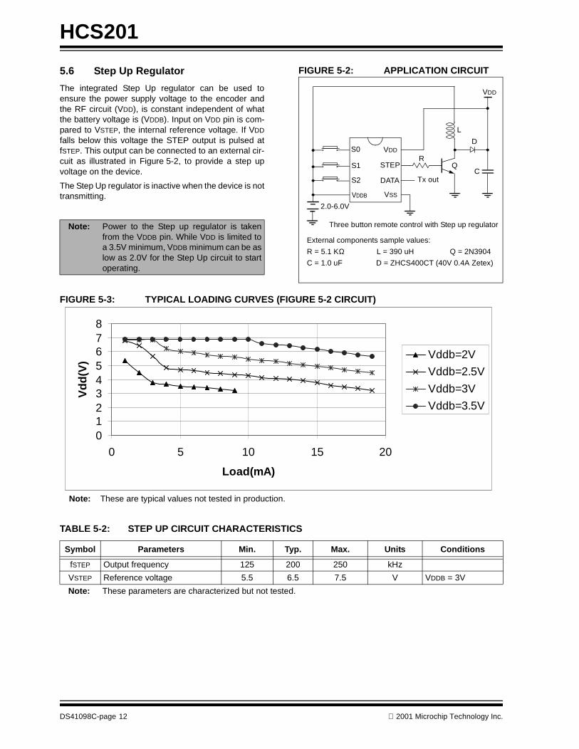
5.6 Step Up Regulator
The integrated Step Up regulator can be used toensure the power supply voltage to the encoder andthe RF circuit (VDD), is constant independent of whatthe battery voltage is (VDDB). Input on VDD pin is com-pared to VSTEP, the internal reference voltage. If VDD
falls below this voltage the STEP output is pulsed atfSTEP. This output can be connected to an external cir-cuit as illustrated in Figure 5-2, to provide a step upvoltage on the device.
The Step Up regulator is inactive when the device is nottransmitting.
FIGURE 5-2: APPLICATION CIRCUIT
FIGURE 5-3: TYPICAL LOADING CURVES (FIGURE 5-2 CIRCUIT)
TABLE 5-2: STEP UP CIRCUIT CHARACTERISTICS
Note: Power to the Step up regulator is takenfrom the VDDB pin. While VDD is limited toa 3.5V minimum, VDDB minimum can be aslow as 2.0V for the Step Up circuit to startoperating.
S0
S1
S2
STEP
VDD
DATA
VSSVDDB
VDD
Tx out
Three button remote control with Step up regulator
2.0-6.0V
External components sample values:
R = 5.1 KΩ L = 390 uH Q = 2N3904
C = 1.0 uF D = ZHCS400CT (40V 0.4A Zetex)
R
L
D
CQ
Symbol Parameters Min. Typ. Max. Units Conditions
fSTEP Output frequency 125 200 250 kHz
VSTEP Reference voltage 5.5 6.5 7.5 V VDDB = 3V
Note: These parameters are characterized but not tested.
012345678
0 5 10 15 20
Load(mA)
Vd
d(V
) Vddb=2V
Vddb=2.5V
Vddb=3V
Vddb=3.5V
Note: These are typical values not tested in production.
DS41098C-page 12 2001 Microchip Technology Inc.

HCS201
6.0 PROGRAMMING THE HCS201
When using the HCS201 in a system, the user will haveto program some parameters into the device includingthe serial number and the secret key before it can beused. The programming cycle allows the user to inputall 192 bits in a serial data stream, which are thenstored internally in EEPROM. Programming will beinitiated by forcing the DATA line high, after the S2 linehas been held high for the appropriate length of timeline (Table 6-1 and Figure 6-1). After the Programmode is entered, a delay must be provided to thedevice for the automatic bulk write cycle to complete.This will write all locations in the EEPROM to an allzeros pattern. The device can then be programmed byclocking in 16 bits at a time, using S2 as the clock lineand DATA as the data in line. After each 16-bit word isloaded, a programming delay is required for the internalprogram cycle to complete. This delay can take up to
Twc. After every 16-bit word is written to the HCS201,the HCS201 will signal that the write is complete bysending out a train of ACK pulses, TACKH high, TACKL
low (if the oscillator was perfectly tuned) on DATA.These will continue until S2 is dropped. The first pulse’swidth should NOT be used for calibration. At the end ofthe programming cycle, the device can be verified(Figure 6-2) by reading back the EEPROM. Reading isdone by clocking the S2 line and reading the data bitson DATA. For security reasons, it is not possible to exe-cute a verify function without first programming theEEPROM. A Verify operation can only be doneonce, immediately following the Program cycle.
FIGURE 6-1: PROGRAMMING WAVEFORMS
FIGURE 6-2: VERIFY WAVEFORMS
Note: To ensure that the device does not acci-dentally enter Programming mode, DATAshould never be pulled high by the circuitconnected to it. Special care should betaken when driving PNP RF transistors.
DATA
Enter Program Mode
(Data)
(Clock)
Note 1: S0 and S1 button inputs to be held to ground during the entire programming sequence.
Bit 0 Bit 1 Bit 2 Bit 3 Bit 14 Bit 15 Bit 16 Bit 17
TPH1
TPBW
TPS
Repeat for each word (12 times)
TPH2
TCLKH
TCLKLTWC
TDS
S2
Data for Word 1
TDH
TCLKL
Initiate DataPolling Here
Write CycleComplete Here
TACKL
TACKH
Calibration Pulses
TPHOLD
Ack Ack Ack
DATA
(Clock)
(Data)
Note: If a Verify operation is to be done, then it must immediately follow the Program cycle.
End of Programming Cycle Beginning of Verify Cycle
Bit 1 Bit 2 Bit 3 Bit 15Bit 14 Bit 16 Bit 17 Bit190 Bit191
TWC
Data from Word 0
TDV
S2
Bit 0Bit191Bit190 Ack
2001 Microchip Technology Inc. DS41098C-page 13
HCS201
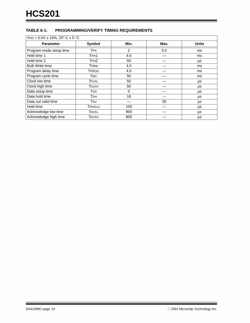
TABLE 6-1: PROGRAMMING/VERIFY TIMING REQUIREMENTS
VDD = 5.0V ± 10%, 25° C ± 5 °CParameter Symbol Min. Max. Units
Program mode setup time TPS 2 5.0 msHold time 1 TPH1 4.0 — msHold time 2 TPH2 50 — µsBulk Write time TPBW 4.0 — msProgram delay time TPROG 4.0 — msProgram cycle time TWC 50 — msClock low time TCLKL 50 — µsClock high time TCLKH 50 — µsData setup time TDS 0 — µsData hold time TDH 18 — µsData out valid time TDV — 30 µsHold time TPHOLD 100 — µsAcknowledge low time TACKL 800 — µsAcknowledge high time TACKH 800 — µs
DS41098C-page 14 2001 Microchip Technology Inc.
HCS201
7.0 INTEGRATING THE HCS201 INTO A SYSTEM
Use of the HCS201 in a system requires a compatibledecoder. This decoder is typically a microcontroller withcompatible firmware. Microchip will provide (via alicense agreement) firmware routines that accepttransmissions from the HCS201 and decrypt thehopping code portion of the data stream. Theseroutines provide system designers the means todevelop their own decoding system.
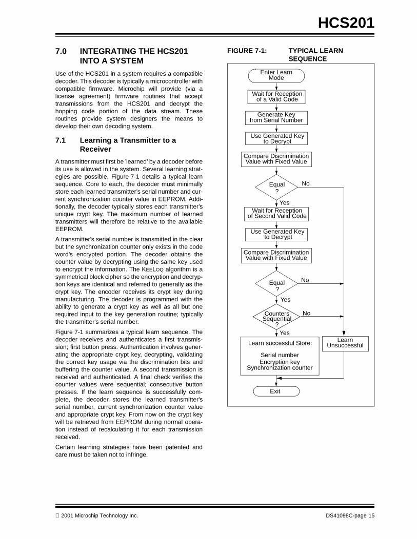
7.1 Learning a Transmitter to a Receiver
A transmitter must first be ’learned’ by a decoder beforeits use is allowed in the system. Several learning strat-egies are possible, Figure 7-1 details a typical learnsequence. Core to each, the decoder must minimallystore each learned transmitter’s serial number and cur-rent synchronization counter value in EEPROM. Addi-tionally, the decoder typically stores each transmitter’sunique crypt key. The maximum number of learnedtransmitters will therefore be relative to the availableEEPROM.
A transmitter’s serial number is transmitted in the clearbut the synchronization counter only exists in the codeword’s encrypted portion. The decoder obtains thecounter value by decrypting using the same key usedto encrypt the information. The KEELOQ algorithm is asymmetrical block cipher so the encryption and decryp-tion keys are identical and referred to generally as thecrypt key. The encoder receives its crypt key duringmanufacturing. The decoder is programmed with theability to generate a crypt key as well as all but onerequired input to the key generation routine; typicallythe transmitter’s serial number.
Figure 7-1 summarizes a typical learn sequence. Thedecoder receives and authenticates a first transmis-sion; first button press. Authentication involves gener-ating the appropriate crypt key, decrypting, validatingthe correct key usage via the discrimination bits andbuffering the counter value. A second transmission isreceived and authenticated. A final check verifies thecounter values were sequential; consecutive buttonpresses. If the learn sequence is successfully com-plete, the decoder stores the learned transmitter’sserial number, current synchronization counter valueand appropriate crypt key. From now on the crypt keywill be retrieved from EEPROM during normal opera-tion instead of recalculating it for each transmissionreceived.
Certain learning strategies have been patented andcare must be taken not to infringe.
FIGURE 7-1: TYPICAL LEARN SEQUENCE
Enter LearnMode
Wait for Receptionof a Valid Code
Generate Keyfrom Serial Number
Use Generated Keyto Decrypt
Compare DiscriminationValue with Fixed Value
Equal
Wait for Receptionof Second Valid Code
Compare DiscriminationValue with Fixed Value
Use Generated Key to Decrypt
Equal
Counters
Encryption keySerial number
Synchronization counter
Sequential?
?
?
Exit
Learn successful Store: LearnUnsuccessful
No
No
No
Yes
Yes
Yes
2001 Microchip Technology Inc. DS41098C-page 15
HCS201
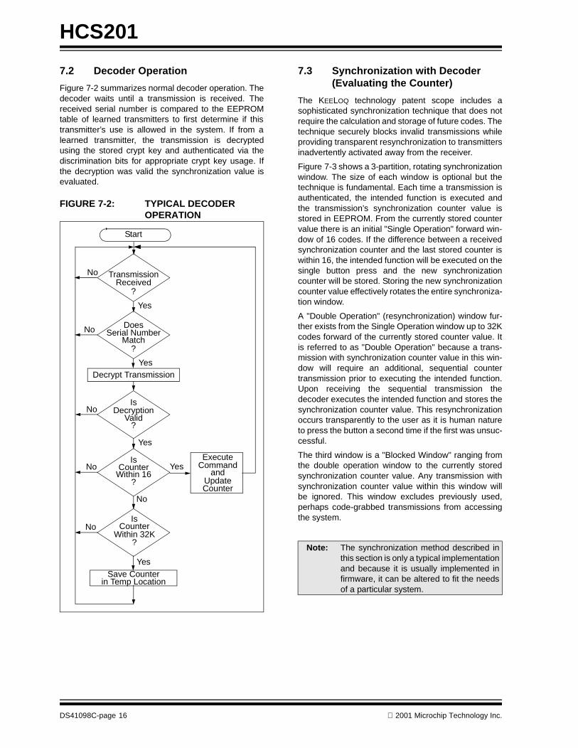
7.2 Decoder Operation
Figure 7-2 summarizes normal decoder operation. Thedecoder waits until a transmission is received. Thereceived serial number is compared to the EEPROMtable of learned transmitters to first determine if thistransmitter’s use is allowed in the system. If from alearned transmitter, the transmission is decryptedusing the stored crypt key and authenticated via thediscrimination bits for appropriate crypt key usage. Ifthe decryption was valid the synchronization value isevaluated.
FIGURE 7-2: TYPICAL DECODER OPERATION
7.3 Synchronization with Decoder (Evaluating the Counter)
The KEELOQ technology patent scope includes asophisticated synchronization technique that does notrequire the calculation and storage of future codes. Thetechnique securely blocks invalid transmissions whileproviding transparent resynchronization to transmittersinadvertently activated away from the receiver.
Figure 7-3 shows a 3-partition, rotating synchronizationwindow. The size of each window is optional but thetechnique is fundamental. Each time a transmission isauthenticated, the intended function is executed andthe transmission’s synchronization counter value isstored in EEPROM. From the currently stored countervalue there is an initial "Single Operation" forward win-dow of 16 codes. If the difference between a receivedsynchronization counter and the last stored counter iswithin 16, the intended function will be executed on thesingle button press and the new synchronizationcounter will be stored. Storing the new synchronizationcounter value effectively rotates the entire synchroniza-tion window.
A "Double Operation" (resynchronization) window fur-ther exists from the Single Operation window up to 32Kcodes forward of the currently stored counter value. Itis referred to as "Double Operation" because a trans-mission with synchronization counter value in this win-dow will require an additional, sequential countertransmission prior to executing the intended function.Upon receiving the sequential transmission thedecoder executes the intended function and stores thesynchronization counter value. This resynchronizationoccurs transparently to the user as it is human natureto press the button a second time if the first was unsuc-cessful.
The third window is a "Blocked Window" ranging fromthe double operation window to the currently storedsynchronization counter value. Any transmission withsynchronization counter value within this window willbe ignored. This window excludes previously used,perhaps code-grabbed transmissions from accessingthe system.
?
TransmissionReceived
DoesSerial Number
Match?
Decrypt Transmission
IsDecryption
Valid?
IsCounter
Within 16?
IsCounter
Within 32K?
UpdateCounter
ExecuteCommand
Save Counterin Temp Location
Start
No
No
No
No
Yes
Yes
Yes
Yes
Yes
No
andNo
Note: The synchronization method described inthis section is only a typical implementationand because it is usually implemented infirmware, it can be altered to fit the needsof a particular system.
DS41098C-page 16 2001 Microchip Technology Inc.

HCS201
FIGURE 7-3: SYNCHRONIZATION WINDOW
Blocked
Entire Window rotates to eliminateuse of previouslyused codes
Single OperationWindow
Window(32K Codes)
(16 Codes)
Double Operation(resynchronization)
Window (32K Codes)
StoredSynchronizationCounter Value
2001 Microchip Technology Inc. DS41098C-page 17

HCS201
8.0 ELECTRICAL CHARACTERISTICS
TABLE 8-1: ABSOLUTE MAXIMUM RATINGS
TABLE 8-2: DC CHARACTERISTICS
Symbol Item Rating Units
VDD Supply voltage -0.3 to 13.5 V
VIN Input voltage -0.3 to VDD + 0.3 V
VOUT Output voltage -0.3 to VDD + 0.3 V
IOUT Max output current 50 mA
TSTG Storage temperature -55 to +125 C (Note 1)
TLSOL Lead soldering temp 300 C (Note 1)
Note 1: Stresses above those listed under “ABSOLUTE MAXIMUM RATINGS” may cause permanent damage to the device.
Commercial (C): Tamb = 0°C to +70°CIndustrial (I): Tamb = -40°C to +85°C
3.5V < VDD < 5.0V 5.0V < VDD < 13.0V
Parameter Sym. Min. Typ.1 Max. Min. Typ.1 Max. Unit Conditions
OperatingCurrent (avg)2
ICC — 0.2 0.5 — —1.5
—2
mAmA
StandbyCurrent
ICCS — 0.1 1.0 — 0.1 1.0 µA
Auto-shutoffCurrent3,4
ICCS — 40 75 — 160 300 µA
High LevelInput Voltage
VIH 0.55VDD — VDD+0.3 2.75 — VDD+0.3 V
Low levelInput Voltage
VIL -0.3 — 0.15VDD -0.3 — 0.75 V
High levelOutput Voltage
VOH 0.6VDD — — —3.3
— — VV
IOH = -1.0 mA VDD = 3.5VIOH = -2.0 mA VDD = 12V
Low LevelOutput Voltage
VOL — — 0.08VDD — — —0.4
VV
IOL = 1.0 mA VDD = 5VIOL = 2.0 mA VDD = 12V
Pull-down Resistance;S0-S2
RSO-2 40 60 80 40 60 80 kΩ VDD = 4.0V
Pull-down Resistance; DATA
RDATA 80 120 160 80 120 160 kΩ VDD = 4.0V
Note 1: Typical values are at 25°C.
2: No load.
3: Auto-shutoff current specification does not include the current through the input pull-down resistors.
4: These values are characterized but not tested.
DS41098C-page 18 2001 Microchip Technology Inc.
HCS201
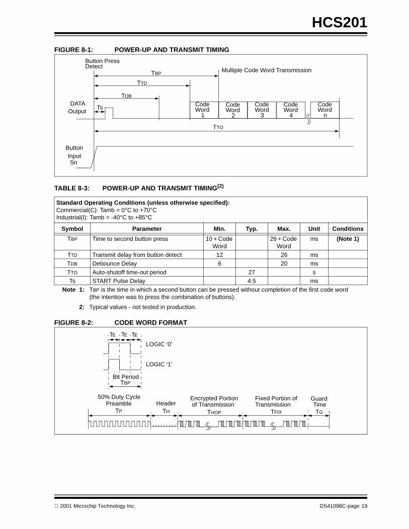
FIGURE 8-1: POWER-UP AND TRANSMIT TIMING
TABLE 8-3: POWER-UP AND TRANSMIT TIMING(2)
FIGURE 8-2: CODE WORD FORMAT
Standard Operating Conditions (unless otherwise specified):Commercial(C): Tamb = 0°C to +70°CIndustrial(I): Tamb = -40°C to +85°C
Symbol Parameter Min. Typ. Max. Unit Conditions
TBP Time to second button press 10 + Code Word
26 + Code Word
ms (Note 1)
TTD Transmit delay from button detect 12 26 msTDB Debounce Delay 6 20 ms
TTO Auto-shutoff time-out period 27 sTs START Pulse Delay 4.5 ms
Note 1: TBP is the time in which a second button can be pressed without completion of the first code word (the intention was to press the combination of buttons).
2: Typical values - not tested in production.
Button Press
Sn
Detect
TDB
Output
TTD
Multiple Code Word Transmission
TTO
CodeWord 1
CodeWord 2
CodeWord 3
CodeWord n
TBP
CodeWord 4
DATA
InputButton
TS
LOGIC ‘0’
LOGIC ‘1’
Bit Period
Preamble HeaderEncrypted Portion of Transmission
Fixed Portion ofTransmission
Guard Time
TP TH THOP TFIX TG
50% Duty Cycle
TBP
TETETE
2001 Microchip Technology Inc. DS41098C-page 19
HCS201
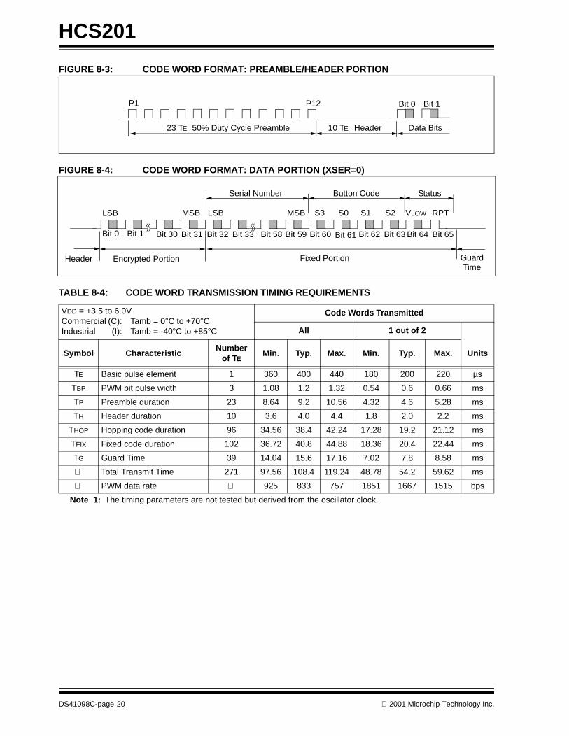
FIGURE 8-3: CODE WORD FORMAT: PREAMBLE/HEADER PORTION
FIGURE 8-4: CODE WORD FORMAT: DATA PORTION (XSER=0)
TABLE 8-4: CODE WORD TRANSMISSION TIMING REQUIREMENTS
VDD = +3.5 to 6.0VCommercial (C): Tamb = 0°C to +70°CIndustrial (I): Tamb = -40°C to +85°C
Code Words Transmitted
All 1 out of 2
Symbol CharacteristicNumber
of TEMin. Typ. Max. Min. Typ. Max. Units
TE Basic pulse element 1 360 400 440 180 200 220 µs
TBP PWM bit pulse width 3 1.08 1.2 1.32 0.54 0.6 0.66 ms
TP Preamble duration 23 8.64 9.2 10.56 4.32 4.6 5.28 ms
TH Header duration 10 3.6 4.0 4.4 1.8 2.0 2.2 ms
THOP Hopping code duration 96 34.56 38.4 42.24 17.28 19.2 21.12 ms
TFIX Fixed code duration 102 36.72 40.8 44.88 18.36 20.4 22.44 ms
TG Guard Time 39 14.04 15.6 17.16 7.02 7.8 8.58 ms
Total Transmit Time 271 97.56 108.4 119.24 48.78 54.2 59.62 ms
PWM data rate 925 833 757 1851 1667 1515 bps
Note 1: The timing parameters are not tested but derived from the oscillator clock.
50% Duty Cycle Preamble Header
P1 P12
23 TE 10 TE Data Bits
Bit 0 Bit 1
Bit 0 Bit 1
Header
Bit 30 Bit 31 Bit 32 Bit 33 Bit 58 Bit 59
Fixed PortionEncrypted Portion Guard
LSBLSB MSB MSB S3 S0 S1 S2 VLOW RPT
Time
Serial Number Button Code Status
Bit 60 Bit 61 Bit 62 Bit 63 Bit 64 Bit 65
DS41098C-page 20 2001 Microchip Technology Inc.

HCS201
9.0 PACKAGING INFORMATION
9.1 Package Marking Information
XXXXXXXXXXXXXNNN
YYWW
8-Lead PDIP (300 mil) Example
HCS201XXXXXNNN
0025
8-Lead SOIC (150 mil) Example
Legend: XX...X Customer specific information*YY Year code (last 2 digits of calendar year)WW Week code (week of January 1 is week ‘01’)NNN Alphanumeric traceability code
Note: In the event the full Microchip part number cannot be marked on one line, it willbe carried over to the next line thus limiting the number of available charactersfor customer specific information.
* Standard OTP marking consists of Microchip part number, year code, week code, facility code, maskrev#, and assembly code. For OTP marking beyond this, certain price adders apply. Please check withyour Microchip Sales Office. For QTP devices, any special marking adders are included in QTP price.
XXXXXXXXXXYYWW
NNN
HCS201XXX0025
NNN
2001 Microchip Technology Inc. DS41098C-page 21
HCS201
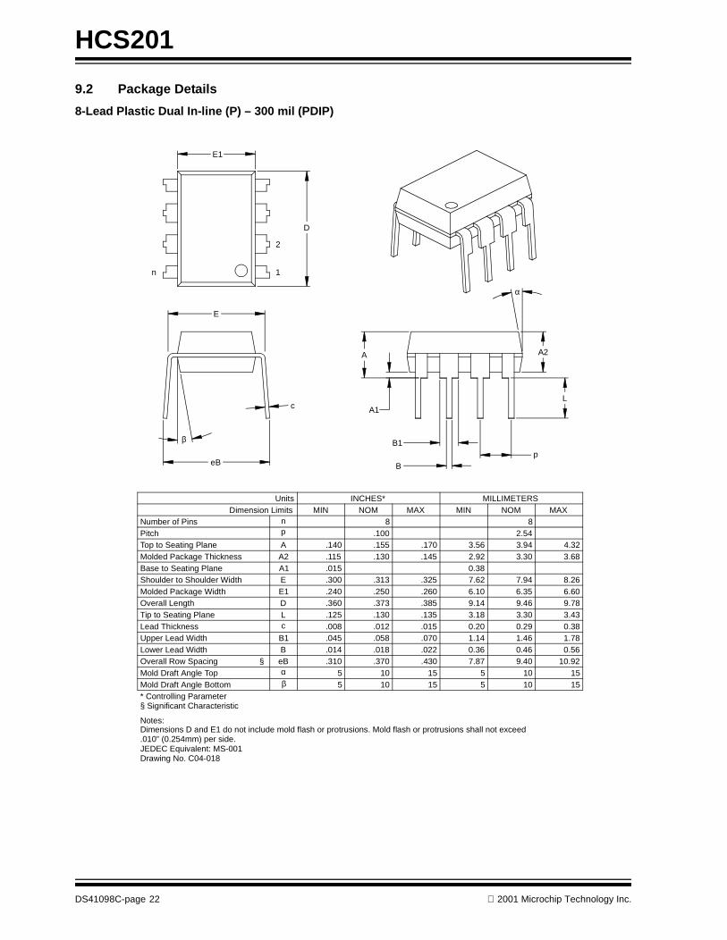
9.2 Package Details
8-Lead Plastic Dual In-line (P) – 300 mil (PDIP)
B1
B
A1
A
L
A2
p
α
E
eB
β
c
E1
n
D
1
2
Units INCHES* MILLIMETERSDimension Limits MIN NOM MAX MIN NOM MAX
Number of Pins n 8 8Pitch p .100 2.54Top to Seating Plane A .140 .155 .170 3.56 3.94 4.32Molded Package Thickness A2 .115 .130 .145 2.92 3.30 3.68Base to Seating Plane A1 .015 0.38Shoulder to Shoulder Width E .300 .313 .325 7.62 7.94 8.26Molded Package Width E1 .240 .250 .260 6.10 6.35 6.60Overall Length D .360 .373 .385 9.14 9.46 9.78Tip to Seating Plane L .125 .130 .135 3.18 3.30 3.43Lead Thickness c .008 .012 .015 0.20 0.29 0.38Upper Lead Width B1 .045 .058 .070 1.14 1.46 1.78Lower Lead Width B .014 .018 .022 0.36 0.46 0.56Overall Row Spacing § eB .310 .370 .430 7.87 9.40 10.92Mold Draft Angle Top α 5 10 15 5 10 15Mold Draft Angle Bottom β 5 10 15 5 10 15* Controlling Parameter
Notes:Dimensions D and E1 do not include mold flash or protrusions. Mold flash or protrusions shall not exceed
JEDEC Equivalent: MS-001Drawing No. C04-018
.010” (0.254mm) per side.
§ Significant Characteristic
DS41098C-page 22 2001 Microchip Technology Inc.
HCS201
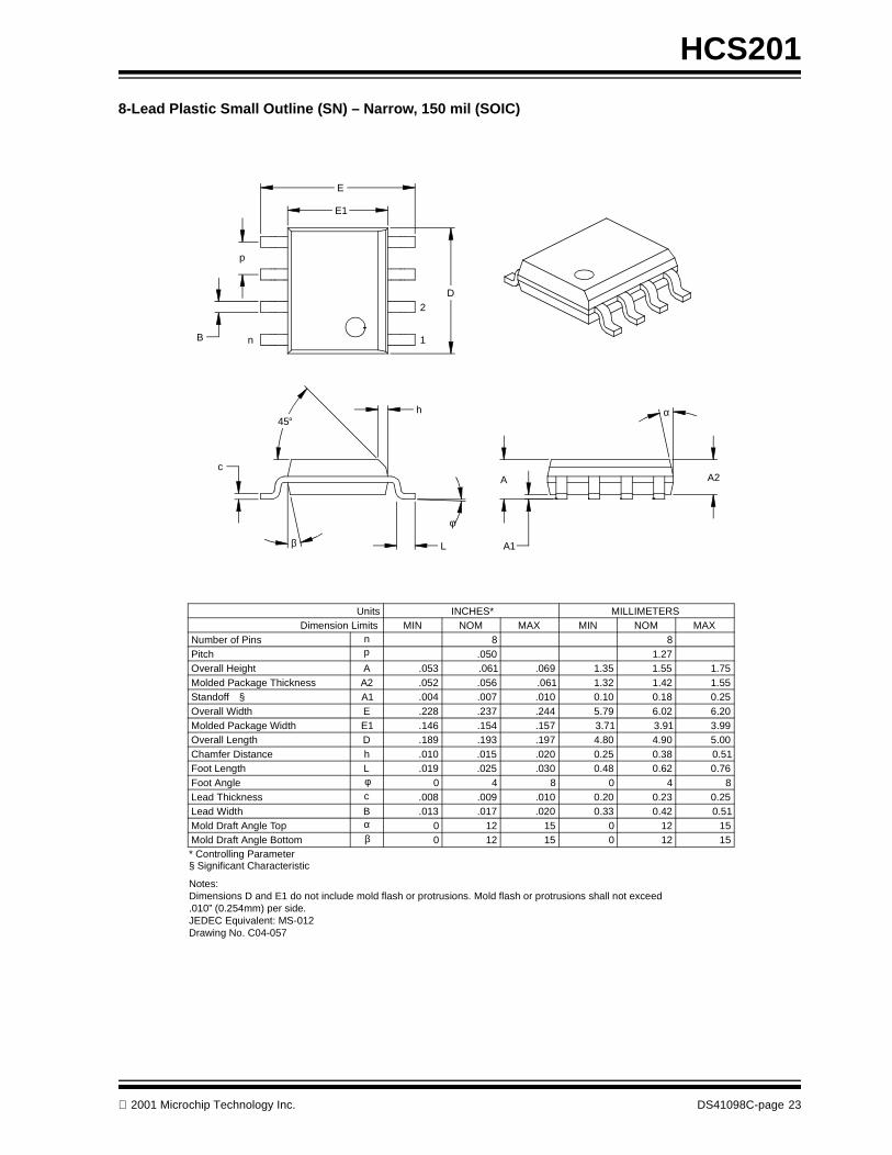
8-Lead Plastic Small Outline (SN) – Narrow, 150 mil (SOIC)
Foot Angle φ 0 4 8 0 4 8
1512015120βMold Draft Angle Bottom1512015120αMold Draft Angle Top
0.510.420.33.020.017.013BLead Width0.250.230.20.010.009.008cLead Thickness
0.760.620.48.030.025.019LFoot Length0.510.380.25.020.015.010hChamfer Distance5.004.904.80.197.193.189DOverall Length3.993.913.71.157.154.146E1Molded Package Width6.206.025.79.244.237.228EOverall Width0.250.180.10.010.007.004A1Standoff §1.551.421.32.061.056.052A2Molded Package Thickness1.751.551.35.069.061.053AOverall Height
1.27.050pPitch88nNumber of Pins
MAXNOMMINMAXNOMMINDimension LimitsMILLIMETERSINCHES*Units
2
1
D
n
p
B
E
E1
h
Lβ
c
45°
φ
A2
α
A
A1
* Controlling Parameter
Notes:Dimensions D and E1 do not include mold flash or protrusions. Mold flash or protrusions shall not exceed .010” (0.254mm) per side.JEDEC Equivalent: MS-012Drawing No. C04-057
§ Significant Characteristic
2001 Microchip Technology Inc. DS41098C-page 23

HCS201
ON-LINE SUPPORT
Microchip provides on-line support on the MicrochipWorld Wide Web (WWW) site.
The web site is used by Microchip as a means to makefiles and information easily available to customers. Toview the site, the user must have access to the Internetand a web browser, such as Netscape or MicrosoftExplorer. Files are also available for FTP downloadfrom our FTP site.
Connecting to the Microchip Internet Web Site
The Microchip web site is available by using yourfavorite Internet browser to attach to:
www.microchip.com
The file transfer site is available by using an FTP ser-vice to connect to:
ftp://ftp.microchip.com
The web site and file transfer site provide a variety ofservices. Users may download files for the latestDevelopment Tools, Data Sheets, Application Notes,User’s Guides, Articles and Sample Programs. A vari-ety of Microchip specific business information is alsoavailable, including listings of Microchip sales offices,distributors and factory representatives. Other dataavailable for consideration is:
• Latest Microchip Press Releases
• Technical Support Section with Frequently Asked Questions
• Design Tips• Device Errata• Job Postings
• Microchip Consultant Program Member Listing• Links to other useful web sites related to
Microchip Products• Conferences for products, Development Systems,
technical information and more• Listing of seminars and events
Systems Information and Upgrade Hot Line
The Systems Information and Upgrade Line providessystem users a listing of the latest versions of all ofMicrochip's development systems software products.Plus, this line provides information on how customerscan receive any currently available upgrade kits.TheHot Line Numbers are:
1-800-755-2345 for U.S. and most of Canada, and
1-480-792-7302 for the rest of the world.
DS41098C-page 24 2001 Microchip Technology Inc.

HCS201
READER RESPONSE
It is our intention to provide you with the best documentation possible to ensure successful use of your Microchip prod-uct. If you wish to provide your comments on organization, clarity, subject matter, and ways in which our documentationcan better serve you, please FAX your comments to the Technical Publications Manager at (480) 792-7578.
Please list the following information, and use this outline to provide us with your comments about this Data Sheet.
To: Technical Publications Manager
RE: Reader Response
Total Pages Sent
From: Name
Company
Address
City / State / ZIP / Country
Telephone: (_______) _________ - _________
Application (optional):
Would you like a reply? Y N
Device: Literature Number:
Questions:
FAX: (______) _________ - _________
DS41098CHCS201
1. What are the best features of this document?
2. How does this document meet your hardware and software development needs?
3. Do you find the organization of this data sheet easy to follow? If not, why?
4. What additions to the data sheet do you think would enhance the structure and subject?
5. What deletions from the data sheet could be made without affecting the overall usefulness?
6. Is there any incorrect or misleading information (what and where)?
7. How would you improve this document?
8. How would you improve our software, systems, and silicon products?
2001 Microchip Technology Inc. DS41098C-page 25
HCS201
NOTES:
DS41098C-page 26 2001 Microchip Technology Inc.
Microchip’s Secure Data Products are covered by some or all of the following patents:Code hopping encoder patents issued in Europe, U.S.A., and R.S.A. — U.S.A.: 5,517,187; Europe: 0459781; R.S.A.: ZA93/4726Secure learning patents issued in the U.S.A. and R.S.A. — U.S.A.: 5,686,904; R.S.A.: 95/5429
Information contained in this publication regarding deviceapplications and the like is intended through suggestion onlyand may be superseded by updates. It is your responsibility toensure that your application meets with your specifications.No representation or warranty is given and no liability isassumed by Microchip Technology Incorporated with respectto the accuracy or use of such information, or infringement ofpatents or other intellectual property rights arising from suchuse or otherwise. Use of Microchip’s products as critical com-ponents in life support systems is not authorized except withexpress written approval by Microchip. No licenses are con-veyed, implicitly or otherwise, under any intellectual propertyrights.
2001 Microchip Technology Inc.
Trademarks
The Microchip name and logo, the Microchip logo, FilterLab,KEELOQ, MPLAB, PIC, PICmicro, PICMASTER, PICSTART,PRO MATE, SEEVAL and The Embedded Control SolutionsCompany are registered trademarks of Microchip TechnologyIncorporated in the U.S.A. and other countries.
dsPIC, ECONOMONITOR, FanSense, FlexROM, fuzzyLAB,In-Circuit Serial Programming, ICSP, ICEPIC, microID,microPort, Migratable Memory, MPASM, MPLIB, MPLINK,MPSIM, MXDEV, PICC, PICDEM, PICDEM.net, rfPIC, SelectMode and Total Endurance are trademarks of MicrochipTechnology Incorporated in the U.S.A.
Serialized Quick Turn Programming (SQTP) is a service markof Microchip Technology Incorporated in the U.S.A.
All other trademarks mentioned herein are property of theirrespective companies.
© 2001, Microchip Technology Incorporated, Printed in theU.S.A., All Rights Reserved.
Printed on recycled paper.
DS41098C - page 27
Microchip received QS-9000 quality system certification for its worldwide headquarters, design and wafer fabrication facilities in Chandler and Tempe, Arizona in July 1999. The Company’s quality system processes and procedures are QS-9000 compliant for its PICmicro® 8-bit MCUs, KEELOQ® code hopping devices, Serial EEPROMs and microperipheral products. In addition, Microchip’s quality system for the design and manufacture of development systems is ISO 9001 certified.
DS41098C-page 28 2001 Microchip Technology Inc.
AMERICASCorporate Office2355 West Chandler Blvd.Chandler, AZ 85224-6199Tel: 480-792-7200 Fax: 480-792-7277Technical Support: 480-792-7627Web Address: http://www.microchip.comRocky Mountain2355 West Chandler Blvd.Chandler, AZ 85224-6199Tel: 480-792-7966 Fax: 480-792-7456
Atlanta500 Sugar Mill Road, Suite 200BAtlanta, GA 30350Tel: 770-640-0034 Fax: 770-640-0307Boston2 Lan Drive, Suite 120Westford, MA 01886Tel: 978-692-3848 Fax: 978-692-3821Chicago333 Pierce Road, Suite 180Itasca, IL 60143Tel: 630-285-0071 Fax: 630-285-0075Dallas4570 Westgrove Drive, Suite 160Addison, TX 75001Tel: 972-818-7423 Fax: 972-818-2924DaytonTwo Prestige Place, Suite 130Miamisburg, OH 45342Tel: 937-291-1654 Fax: 937-291-9175DetroitTri-Atria Office Building 32255 Northwestern Highway, Suite 190Farmington Hills, MI 48334Tel: 248-538-2250 Fax: 248-538-2260Kokomo2767 S. Albright Road Kokomo, Indiana 46902Tel: 765-864-8360 Fax: 765-864-8387Los Angeles18201 Von Karman, Suite 1090Irvine, CA 92612Tel: 949-263-1888 Fax: 949-263-1338New York150 Motor Parkway, Suite 202Hauppauge, NY 11788Tel: 631-273-5305 Fax: 631-273-5335San JoseMicrochip Technology Inc.2107 North First Street, Suite 590San Jose, CA 95131Tel: 408-436-7950 Fax: 408-436-7955Toronto6285 Northam Drive, Suite 108Mississauga, Ontario L4V 1X5, CanadaTel: 905-673-0699 Fax: 905-673-6509
ASIA/PACIFICAustraliaMicrochip Technology Australia Pty LtdSuite 22, 41 Rawson StreetEpping 2121, NSWAustraliaTel: 61-2-9868-6733 Fax: 61-2-9868-6755China - BeijingMicrochip Technology Consulting (Shanghai)Co., Ltd., Beijing Liaison OfficeUnit 915Bei Hai Wan Tai Bldg.No. 6 Chaoyangmen Beidajie Beijing, 100027, No. ChinaTel: 86-10-85282100 Fax: 86-10-85282104China - ChengduMicrochip Technology Consulting (Shanghai)Co., Ltd., Chengdu Liaison OfficeRm. 2401, 24th Floor, Ming Xing Financial TowerNo. 88 TIDU StreetChengdu 610016, ChinaTel: 86-28-6766200 Fax: 86-28-6766599China - FuzhouMicrochip Technology Consulting (Shanghai)Co., Ltd., Fuzhou Liaison OfficeRm. 531, North BuildingFujian Foreign Trade Center Hotel73 Wusi RoadFuzhou 350001, ChinaTel: 86-591-7557563 Fax: 86-591-7557572China - ShanghaiMicrochip Technology Consulting (Shanghai)Co., Ltd.Room 701, Bldg. BFar East International PlazaNo. 317 Xian Xia RoadShanghai, 200051Tel: 86-21-6275-5700 Fax: 86-21-6275-5060China - ShenzhenMicrochip Technology Consulting (Shanghai)Co., Ltd., Shenzhen Liaison OfficeRm. 1315, 13/F, Shenzhen Kerry Centre,Renminnan LuShenzhen 518001, ChinaTel: 86-755-2350361 Fax: 86-755-2366086Hong KongMicrochip Technology Hongkong Ltd.Unit 901-6, Tower 2, Metroplaza223 Hing Fong RoadKwai Fong, N.T., Hong KongTel: 852-2401-1200 Fax: 852-2401-3431IndiaMicrochip Technology Inc.India Liaison OfficeDivyasree Chambers1 Floor, Wing A (A3/A4)No. 11, O’Shaugnessey RoadBangalore, 560 025, IndiaTel: 91-80-2290061 Fax: 91-80-2290062
JapanMicrochip Technology Japan K.K.Benex S-1 6F3-18-20, ShinyokohamaKohoku-Ku, Yokohama-shiKanagawa, 222-0033, JapanTel: 81-45-471- 6166 Fax: 81-45-471-6122KoreaMicrochip Technology Korea168-1, Youngbo Bldg. 3 FloorSamsung-Dong, Kangnam-KuSeoul, Korea 135-882Tel: 82-2-554-7200 Fax: 82-2-558-5934SingaporeMicrochip Technology Singapore Pte Ltd.200 Middle Road#07-02 Prime CentreSingapore, 188980Tel: 65-334-8870 Fax: 65-334-8850TaiwanMicrochip Technology Taiwan11F-3, No. 207Tung Hua North RoadTaipei, 105, TaiwanTel: 886-2-2717-7175 Fax: 886-2-2545-0139
EUROPEDenmarkMicrochip Technology Nordic ApSRegus Business CentreLautrup hoj 1-3Ballerup DK-2750 DenmarkTel: 45 4420 9895 Fax: 45 4420 9910FranceMicrochip Technology SARLParc d’Activite du Moulin de Massy43 Rue du Saule TrapuBatiment A - ler Etage91300 Massy, FranceTel: 33-1-69-53-63-20 Fax: 33-1-69-30-90-79GermanyMicrochip Technology GmbHGustav-Heinemann Ring 125D-81739 Munich, GermanyTel: 49-89-627-144 0 Fax: 49-89-627-144-44ItalyMicrochip Technology SRLCentro Direzionale Colleoni Palazzo Taurus 1 V. Le Colleoni 120041 Agrate BrianzaMilan, Italy Tel: 39-039-65791-1 Fax: 39-039-6899883United KingdomArizona Microchip Technology Ltd.505 Eskdale RoadWinnersh TriangleWokingham Berkshire, England RG41 5TUTel: 44 118 921 5869 Fax: 44-118 921-5820
10/01/01
WORLDWIDE SALES AND SERVICE
Recommended