Half-height Pins – a New Pin Form in Gap
Waveguide for Easy Manufacturing
Fangfang Fan1,2, Jian Yang2 and Per-Simon Kildal2
1The Science and Technology on Antenna and Microwave Laboratory, Xidian University, Xi’an, China2Dept. of Signals and Systems, Chalmers University of Technology, S-412 96 Gothenburg, Sweden
E-mail: [email protected], [email protected], [email protected]
Abstract—Gap waveguide is a promising transmission struc-ture, especially for millimeter wave and THz applications. Itdoes not require conductive connection between the top andbottom plates, and therefore this technology gain advantagesover conventional rectangular waveguides and SIWs (SubstrateIntegrated Waveguides) above 100 GHz. In this paper, a new pinform, the half-height pin, is proposed for the gap waveguide. Thisnew half-height pin form has similar stop-band performance asthe previous quarter-wavelength long pin form. However, theremust be such half-height pins on both the upper and lower plates,in contrast to one of the two having pins in the original gapwaveguide. The shorter length of the pins makes the fabricationof the pin surface much easier, such as by e.g. die-forming,molding or MEMS technology. The current work paves the wayfor mass production of gap waveguide devices and systems atmillimeter wave and THz.
Index Terms—gap waveguide, half-height pin, stop-band band-
width.
I. INTRODUCTION
The gap waveguides [1] are realized in the gap between two
parallel metal plates, with periodic metal pins on the bottom
plate to play the role of an AMC (Artificial Magnetic Conduc-
tor), and with a smooth surface on the metal top plate working
as a PEC (Perfect Electrical Conductor). No electromagnetic
waves can propagate in the gap, except along some guiding
structures, such as ridges in the ridge gap waveguides and
grooves in the groove gap waveguides, and only under the
condition that the gap between the top of the pins and the top
plate is smaller than a quarter wavelength. Since the waves
only propagate through air, there is no dielectric losses. Thus,
the gap waveguides have the advantage of lower loss than
microstrip lines and SIWs (Substrate Integrated Waveguide),
where the waves propagate in dielectric materials. In addition,
we can use larger transverse dimensions than in microstrip
lines, and therefore the conductive losses will also be smaller.
Till now, several gap waveguide antennas array [2]–[6] and
components, such as coupler, filter and power divider [7]–
[14] have been designed with good performance, and the gap
waveguide has also been shown to be capable of packaging
passive and active components realized with other transmission
line or waveguide technologies [15].
The fact that the gap waveguide does not require conductive
connection between the top and the bottom plates opens up
for more cost-effective manufacture methods to be used in
millimeter wave and THz applications.
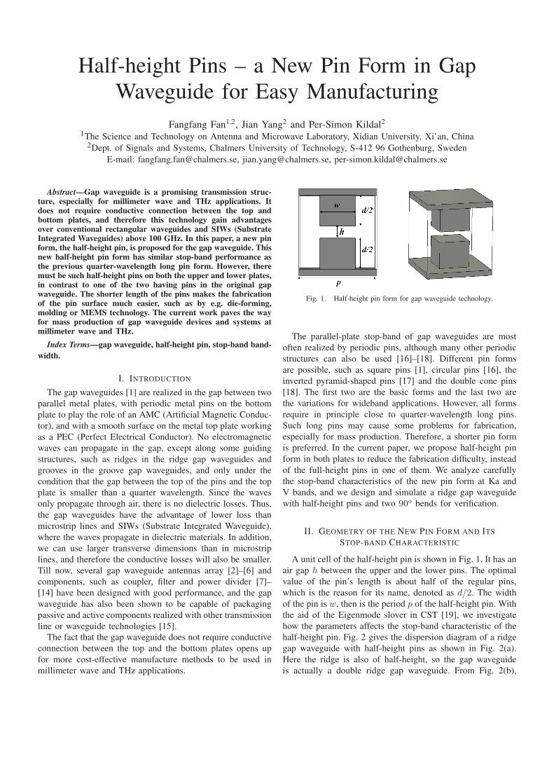
Fig. 1. Half-height pin form for gap waveguide technology.
The parallel-plate stop-band of gap waveguides are most
often realized by periodic pins, although many other periodic
structures can also be used [16]–[18]. Different pin forms
are possible, such as square pins [1], circular pins [16], the
inverted pyramid-shaped pins [17] and the double cone pins
[18]. The first two are the basic forms and the last two are
the variations for wideband applications. However, all forms
require in principle close to quarter-wavelength long pins.
Such long pins may cause some problems for fabrication,
especially for mass production. Therefore, a shorter pin form
is preferred. In the current paper, we propose half-height pin
form in both plates to reduce the fabrication difficulty, instead
of the full-height pins in one of them. We analyze carefully
the stop-band characteristics of the new pin form at Ka and
V bands, and we design and simulate a ridge gap waveguide
with half-height pins and two 90o bends for verification.
II. GEOMETRY OF THE NEW PIN FORM AND ITS
STOP-BAND CHARACTERISTIC
A unit cell of the half-height pin is shown in Fig. 1. It has an
air gap h between the upper and the lower pins. The optimal
value of the pin’s length is about half of the regular pins,
which is the reason for its name, denoted as d/2. The width
of the pin is w, then is the period p of the half-height pin. With
the aid of the Eigenmode slover in CST [19], we investigate
how the parameters affects the stop-band characteristic of the
half-height pin. Fig. 2 gives the dispersion diagram of a ridge
gap waveguide with half-height pins as shown in Fig. 2(a).
Here the ridge is also of half-height, so the gap waveguide
is actually a double ridge gap waveguide. From Fig. 2(b),

(a) The model of the ridge with period pins.
β (
rad/m
)
0
200
400
600
800
1000
1200
1400
1600
Freqeuncy (GHz)
0 20 40 60 80 100 120
Quasi TEM
Light Line
(b) The dispersion diagram.
Fig. 2. Dispersion diagram of the double ridge gap waveguide with half-height pins, where p = 2.08 mm, d = 1.39 mm, h = 0.07 mm, w = 1.25mm.
we can see that the double ridge gap waveguide has a single
dominate (basic) mode propagation band over 31.8-73.2 GHz,
and the propagation mode is a Quasi-TEM mode because its
propagation parameter follows that of the light line.
III. DOUBLE-BEND TRANSMISSION LINE DESIGN AND
THE TRANSITION TO STANDARD WAVEGUIDES
To verify the transmission characteristic of the gap waveg-
uide with new half-height pin form, double ridge gap waveg-
uide with two 90o bends has been designed. Fig. 3 is the
geometry of the transmission line with the two 90o bends.
Here, the waveport used in CST is defined as the width pwand the height ph, where pw is set as the width of the ridge
and plus the spacing to the closest pins on either side, ph is
the height of the double ridge and the air gap between them,
and for these parameters, good transmission can be obtained.
The simulated S parameters are plotted in Fig. 4 and 2D color
figures showing the vertical E field distribution between the
upper and lower ridges are plotted in Fig. 5. As shown in the
figure, the field follows the ridge very well from 30-70 GHz.
Fig. 6 shows the S parameters of two 90o bends transmission
line with regular pins, which has the same dimension with the
half-height pins. It can be concluded they have very similar
transmission characteristic.
Considering the measurement, we need transitions from
standard waveguides to the double ridge gap waveguide with
two 90o bends. Since the operation bandwidth for the gap
waveguide is from 31.8-73.2 GHz, we need two transitions
to different standard waveguides: one to Ka band standard
Fig. 3. Geometry of the double ridge gap waveguide with two 90o bends
based on half-height pins, where wr = 1.8 mm, g = 0.83 mm, dx = dy =
1.45 mm. Note that the upper half is hidden for clear presentation.
Frequency (GHz)
30 35 40 45 50 55 60 65 70 75
S p
ara
mete
rs (
dB
)
-30
-25
-20
-15
-10
-5
0
S11
S21
Fig. 4. The simulated S parameters for the double ridge gap waveguide withtwo 90
o bends based on half-height pins.
Fig. 5. The field distribution of the double ridge gap waveguide with two90
o bends based on half-height pins at different frequencies.
waveguide WR-28 and the other to V band standard waveguide
WR-15. For the Ka band transition, it is not easy to get good
results by simple direct transformation of the geometry since
the size of the gap waveguide will make the dominate modes
at Ka band below cutoff. We tried several different transitions,
and finally we chose a polynomial function profile for the ridge
and cavity as shown in Fig. 7(a). This gave good matching.
The simulated results for this transition are shown in Fig. 8(a),
where the reflection coefficient (S11) is lower than -13 dB over
the whole Ka band. For the V band transition, four stepped
ridges are used, and then the height is changed to the standard
waveguide by tapering, as shown in Fig. 7(b). Fig. 8(b) is the

Frequency (GHz)
30 35 40 45 50 55 60 65 70 75
S p
ara
mete
rs (
dB
)
-30
-25
-20
-15
-10
-5
0S
11
S21
Fig. 6. The simulated S parameters for the double ridge gap waveguide withtwo 90
o bends based on full-height pins.
final results for V band transition and the reflection coefficient
reaches below -14 dB within the transmission band. All the
values of the parameters are given in Table I.
(a) Ka band transition.
(b) V band transition.
Fig. 7. Two transitions from the half-height ridge gap waveguide in Fig. 3 tostandard waveguides WR-28 and WR-15. Note that the upper half is hiddenfor clear presentation.
After connecting the double ridge transmission line in Fig.
3 with the V band transition in Fig. 7(b), we get the results
shown in Fig. 9, it can be seen that the reflection coefficient
reaches below -8 dB within the transmission band.
We are making a prototype for measurement to verify the
simulated results.
In addition, we also have done some simulation work about
the sensitivity for alignment of the top and bottom layer pins.
Frequency (GHz)
26 28 30 32 34 36 38 40
S p
ara
mete
rs (
dB
)
-30
-25
-20
-15
-10
-5
0
S11
S21
(a) Ka band transition.
Frequency (GHz)
50 55 60 65 70 75
S p
ara
mete
rs (
dB
)
-30
-25
-20
-15
-10
-5
0
S11
S21
(b) V band transition.
Fig. 8. Simulated results for the Ka and V band transitions.
Frequency (GHz)
50 55 60 65 70 75
S p
ara
mete
rs (
dB
)
-30
-25
-20
-15
-10
-5
0
S11
S21
Fig. 9. The simulated S parameters for double ridge gap waveguide withtwo 90
o bends with V band transition.
If the alignment offset distance is less than 0.1mm, it will not
influence the transmission performance. Later we will do this
experiment to verify it.
TABLE ITHE PARAMETER VALUES FOR FIG. 7
Parameter la lb ha hb t wt
Value(mm) 2.92 3.15 0.98 1.58 40.1 5.5
Parameter lc ld le lf va vb
Value(mm) 1.18 1.29 1.22 1.30 3.76 1.88
Parameter hc hd he hf wa wb
Value(mm) 0.64 0.45 0.22 0.13 7.11 3.56
IV. CONCLUSION
A new pin form, referred to as the half-height pin, in gap
waveguide technology has been presented. It has a similar
stop-band characteristic as the previous regular full-height
metal pin used in gap waveguide technology, but half-height
pins must be provided at both the upper and lower surfaces,
not only one of them as in the regular gap waveguide. This
reduced height can reduce the fabrication difficulty, especially
for mass production. A double ridge gap waveguide with half-
height pins has been designed for verification. The simulated
results showed that the ridge gap waveguide with the new
pin form has the similar performance as that of the ridge gap
waveguide with regular pins. Thus, this new pin form provides
a flexibility of choosing different pin forms in gap waveguide
technology for low-cost manufacture.
The half-height pin gap waveguide is protected by a pending
patent [20].
ACKNOWLEDGMENT
This work has been supported by the Natural Science
Foundation of China (NSFC) under Grant 61301068, the
Fundamental Research Funds for the Central Universities
(JB150207), the European Research Council (ERC) via an
advanced investigator grant ERC-2012-ADG 20120216 and
Swedish Governmental Agency for Innovation Systems (VIN-
NOVA) within the VINN Excellence Center Chase at Chalmer-
s.
REFERENCES
[1] P.-S. Kildal, E. Alfonso, A. Valero-Nogueira, and E. Rajo-Iglesias,“Local metamaterial-based waveguides in gaps between parallel metalplates,” IEEE Antennas and Wireless Propagation Letters, vol. 8, pp.84–87, 2009.
[2] E. Pucci, E. Rajo-Iglesias, J.-L. Vazquez-Roy, and P.-S. Kildal, “Planardual-mode horn array with corporate-feed network in inverted microstripgap waveguide,” Antennas and Propagation, IEEE Transactions on,vol. 62, no. 7, pp. 3534–3542, 2014.
[3] A. U. Zaman and P.-S. Kildal, “Wide-band slot antenna arrays withsingle-layer corporate-feed network in ridge gap waveguide technology,”Antennas and Propagation, IEEE Transactions on, vol. 62, no. 6, pp.2992–3001, 2014.
[4] M. Al Sharkawy, A. Kishk et al., “Wideband beam-scanning circularlypolarized inclined slots using ridge gap waveguide,” Antennas and
Wireless Propagation Letters, IEEE, vol. 13, pp. 1187–1190, 2014.[5] A. U. Zaman and P.-S. Kildal, “A new 2× 2 microstrip patch sub-
array for 60GHz wideband planar antenna with ridge gap waveguidedistribution layer,” in Antennas and Propagation (EuCAP), 2015 9th
European Conference on. IEEE, 2015, pp. 1–4.
[6] A. U. Zaman, J. Yang, and P.-S. Kildal, “Using lid of pins for packagingof microstrip board for descrambling the ports of eleven antenna forradio telescope applications,” in Antennas and Propagation Society
International Symposium (APSURSI), 2010 IEEE. IEEE, 2010, pp.1–4.
[7] J. Yang and H. Raza, “Empirical formulas for designing gap-waveguidehybrid ring coupler,” Microwave and optical technology letters, vol. 55,no. 8, pp. 1917–1920, 2013.
[8] M. S. Sorkherizi, A. Khaleghi, and P.-S. Kildal, “Direct-coupled cavityfilter in ridge gap waveguide,” IEEE Transactions on Components,
Packaging and Manufacturing Technology, vol. 4, no. 3, pp. 490–495,2014.
[9] E. A. Alos, A. U. Zaman, and P. Kildal, “Ka-band gap waveguidecoupled-resonator filter for radio link diplexer application,” IEEE Trans-
actions on Components, Packaging and Manufacturing Technology,vol. 3, no. 5, pp. 870–879, 2013.
[10] A. U. Zaman, P.-S. Kildal, A. Kishk et al., “Narrow-band microwavefilter using high-Q groove gap waveguide resonators with manufacturingflexibility and no sidewalls,” IEEE Transactions on Components, Pack-
aging and Manufacturing Technology, vol. 2, no. 11, pp. 1882–1889,2012.
[11] A. Berenguer, M. Baquero-Escudero, D. Sanchez-Escuderos,B. Bernardo-Clemente, and V. E. Boria-Esbert, “Low insertion loss 61GHz narrow-band filter implemented with groove gap waveguides,” in2014 44th European Microwave Conference (EuMC). IEEE, 2014,pp. 191–194.
[12] A. del Olmo-Olmeda, M. Baquero-Escudero, V. E. Boria-Esbert,A. Valero-Nogueira, and A. J. Berenguer-Verdu, “A novel band-passfilter topology for millimeter-wave applications based on the groove gapwaveguide,” in 2013 IEEE MTT-S International Microwave Symposium
Digest (IMS). IEEE, 2013, pp. 1–4.[13] H. Raza, J. Yang, P.-S. Kildal, and E. Alfonso Alos, “Microstrip-ridge
gap waveguide–study of losses, bends, and transition to WR-15,” IEEE
Transactions on Microwave Theory and Techniques, vol. 62, no. 9, pp.1943–1952, 2014.
[14] H. Raza and J. Yang, “Compact UWB power divider packaged byusing gap-waveguide technology,” in 2012 6th European Conference
on Antennas and Propagation (EUCAP). IEEE, 2012, pp. 2938–2942.[15] A. U. Zaman, M. Alexanderson, T. Vukusic, and P.-S. Kildal, “Gap
waveguide PMC packaging for improved isolation of circuit componentsin high-frequency microwave modules,” Components, Packaging and
Manufacturing Technology, IEEE Transactions on, vol. 4, no. 1, pp.16–25, 2014.
[16] E. Rajo-Iglesias and P.-S. Kildal, “Numerical studies of bandwidthof parallel-plate cut-off realised by a bed of nails, corrugations andmushroom-type electromagnetic bandgap for use in gap waveguides,”IET microwaves, antennas & propagation, vol. 5, no. 3, pp. 282–289,2011.
[17] A. U. Zaman, V. Vassilev, P.-S. Kildal, and A. Kishk, “Increasing parallelplate stop-band in gap waveguides using inverted pyramid-shaped nailsfor slot array application above 60GHz,” in Proceedings of the 5th
European Conference on Antennas and Propagation (EUCAP). IEEE,2011, pp. 2254–2257.
[18] S. Shams and A. Kishk, “Double cone ultra wide band unit cell inridge gap waveguides,” in 2014 IEEE Antennas and Propagation Society
International Symposium (APSURSI). IEEE, 2014, pp. 1768–1769.[19] CST Microwave Studio; http://www.cst.com.[20] J. Yang and F. Fan, “Waveguides and transmission lines in gaps
between parallel conducting surfaces (half-height pins and double periodpins in both surfaces) ,” European Patent Application EP-15186666.2,
Gapwaves AB Sweden, 24 September 2015.
Recommended