April 2020 AN5031 Rev 2 1/77
1
AN5031Application note
Getting started with STM32MP151, STM32MP153 and STM32MP157 line hardware development
Introduction
This application note shows how to use the STM32MP151, STM32MP153 and STM32MP157 lines, and describes the minimum hardware resources required to develop an application based on those MPU products.
This application note is intended for system designers who require an overview of the hardware implementation of the development board, with focus on features like:
• Power supply
• Package selection
• Clock management
• Reset control
• Boot mode settings
• Debug management.
Reference design schematics are also contained in this document with descriptions of the main components, interfaces and modes.
www.st.com
Contents AN5031
2/77 AN5031 Rev 2
Contents
1 General information . . . . . . . . . . . . . . . . . . . . . . . . . . . . . . . . . . . . . . . . . 8
2 Reference documents . . . . . . . . . . . . . . . . . . . . . . . . . . . . . . . . . . . . . . . . 8
3 Glossary . . . . . . . . . . . . . . . . . . . . . . . . . . . . . . . . . . . . . . . . . . . . . . . . . . . 9
4 Power supplies . . . . . . . . . . . . . . . . . . . . . . . . . . . . . . . . . . . . . . . . . . . . 11
4.1 Introduction . . . . . . . . . . . . . . . . . . . . . . . . . . . . . . . . . . . . . . . . . . . . . . . 12
4.1.1 Independent ADC and DAC converter supply and reference voltage . . 12
4.1.2 Battery backup . . . . . . . . . . . . . . . . . . . . . . . . . . . . . . . . . . . . . . . . . . . . 13
4.1.3 Voltage regulators . . . . . . . . . . . . . . . . . . . . . . . . . . . . . . . . . . . . . . . . . 13
4.2 Power supply schemes . . . . . . . . . . . . . . . . . . . . . . . . . . . . . . . . . . . . . . 14
4.3 Reset and power supply supervisor . . . . . . . . . . . . . . . . . . . . . . . . . . . . . 17
4.3.1 Power on reset (POR) / power down reset (PDR) . . . . . . . . . . . . . . . . . 17
4.3.2 Programmable voltage detector (PVD) . . . . . . . . . . . . . . . . . . . . . . . . . 17
4.3.3 Application and system resets . . . . . . . . . . . . . . . . . . . . . . . . . . . . . . . . 18
5 Packages . . . . . . . . . . . . . . . . . . . . . . . . . . . . . . . . . . . . . . . . . . . . . . . . . 20
5.1 Package selection . . . . . . . . . . . . . . . . . . . . . . . . . . . . . . . . . . . . . . . . . . 20
5.2 Alternate function mapping to pins . . . . . . . . . . . . . . . . . . . . . . . . . . . . . . 22
5.3 Package compatibility between versions . . . . . . . . . . . . . . . . . . . . . . . . . 23
6 Clocks . . . . . . . . . . . . . . . . . . . . . . . . . . . . . . . . . . . . . . . . . . . . . . . . . . . . 28
6.1 HSE OSC clock . . . . . . . . . . . . . . . . . . . . . . . . . . . . . . . . . . . . . . . . . . . . 28
6.1.1 External source (HSE bypass) . . . . . . . . . . . . . . . . . . . . . . . . . . . . . . . . 29
6.1.2 External crystal/ceramic resonator (HSE crystal) . . . . . . . . . . . . . . . . . 29
6.2 LSE OSC clock . . . . . . . . . . . . . . . . . . . . . . . . . . . . . . . . . . . . . . . . . . . . . 30
6.2.1 External source (LSE bypass) . . . . . . . . . . . . . . . . . . . . . . . . . . . . . . . . 30
6.2.2 External crystal/ceramic resonator (LSE crystal) . . . . . . . . . . . . . . . . . . 30
6.3 Clock security system (CSS) . . . . . . . . . . . . . . . . . . . . . . . . . . . . . . . . . . 31
6.3.1 CSS on HSE . . . . . . . . . . . . . . . . . . . . . . . . . . . . . . . . . . . . . . . . . . . . . 31
6.3.2 CSS on LSE . . . . . . . . . . . . . . . . . . . . . . . . . . . . . . . . . . . . . . . . . . . . . . 31
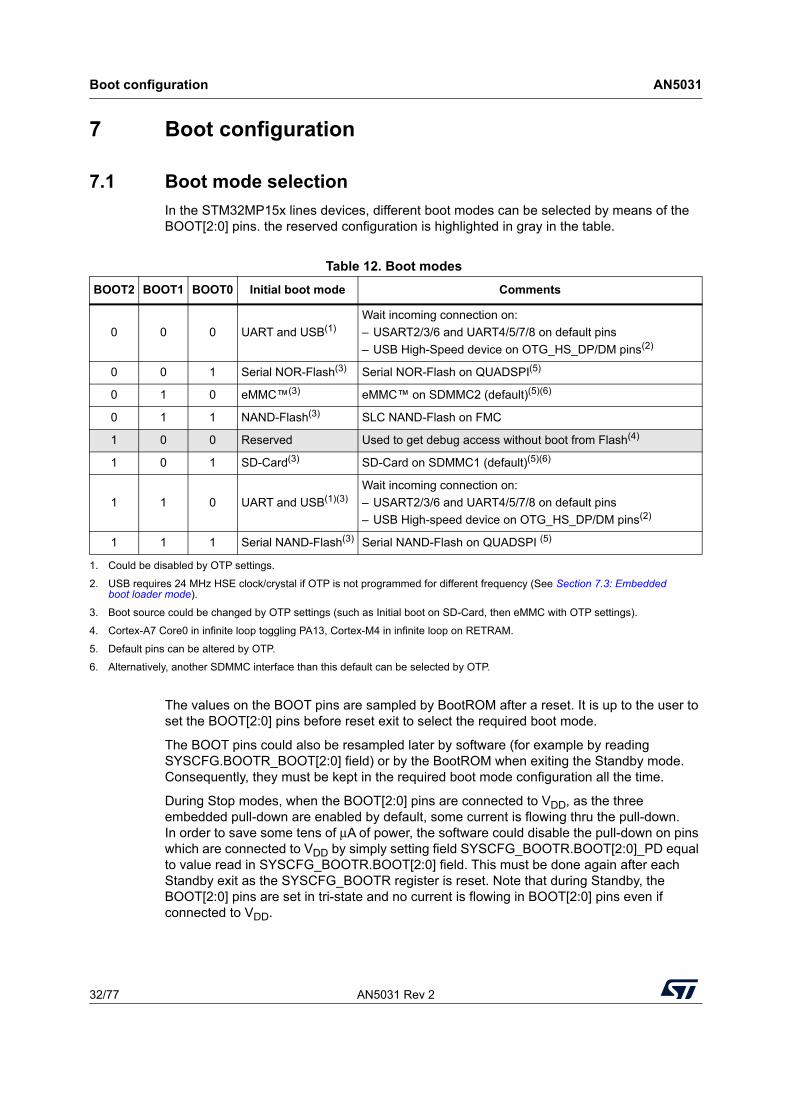
7 Boot configuration . . . . . . . . . . . . . . . . . . . . . . . . . . . . . . . . . . . . . . . . . 32

AN5031 Rev 2 3/77
AN5031 Contents
4
7.1 Boot mode selection . . . . . . . . . . . . . . . . . . . . . . . . . . . . . . . . . . . . . . . . . 32
7.2 Boot pin connection . . . . . . . . . . . . . . . . . . . . . . . . . . . . . . . . . . . . . . . . . 33
7.3 Embedded boot loader mode . . . . . . . . . . . . . . . . . . . . . . . . . . . . . . . . . . 35
8 Debug management . . . . . . . . . . . . . . . . . . . . . . . . . . . . . . . . . . . . . . . . 36
8.1 Introduction . . . . . . . . . . . . . . . . . . . . . . . . . . . . . . . . . . . . . . . . . . . . . . . 36
8.2 SWJ debug port (serial wire and JTAG) . . . . . . . . . . . . . . . . . . . . . . . . . . 36
8.3 Pinout and debug port pins . . . . . . . . . . . . . . . . . . . . . . . . . . . . . . . . . . . 36
8.3.1 Internal pull-up and pull-down resistors on JTAG pins . . . . . . . . . . . . . . 36
8.3.2 Debug port connection with standard JTAG connector . . . . . . . . . . . . . 37
8.3.3 Debug port and UART connection with STDC14 connector . . . . . . . . . 38
8.3.4 Parallel trace and HDP . . . . . . . . . . . . . . . . . . . . . . . . . . . . . . . . . . . . . 39
8.3.5 Debug triggers and LEDs . . . . . . . . . . . . . . . . . . . . . . . . . . . . . . . . . . . 41
9 Recommendations . . . . . . . . . . . . . . . . . . . . . . . . . . . . . . . . . . . . . . . . . 42
9.1 Printed circuit board . . . . . . . . . . . . . . . . . . . . . . . . . . . . . . . . . . . . . . . . . 42
9.2 Component position . . . . . . . . . . . . . . . . . . . . . . . . . . . . . . . . . . . . . . . . . 42
9.3 Ground and power supply (VSSx, VDDx) . . . . . . . . . . . . . . . . . . . . . . . . . . 42
9.4 IO speed settings . . . . . . . . . . . . . . . . . . . . . . . . . . . . . . . . . . . . . . . . . . . 42
9.5 PCB stack and technology . . . . . . . . . . . . . . . . . . . . . . . . . . . . . . . . . . . . 46
9.6 Decoupling . . . . . . . . . . . . . . . . . . . . . . . . . . . . . . . . . . . . . . . . . . . . . . . . 50
9.7 ESD/EMI protections . . . . . . . . . . . . . . . . . . . . . . . . . . . . . . . . . . . . . . . . 50
9.8 Sensitive signals . . . . . . . . . . . . . . . . . . . . . . . . . . . . . . . . . . . . . . . . . . . . 51
9.9 Unused I/Os and features . . . . . . . . . . . . . . . . . . . . . . . . . . . . . . . . . . . . 51
10 Reference design examples . . . . . . . . . . . . . . . . . . . . . . . . . . . . . . . . . . 52
10.1 Description . . . . . . . . . . . . . . . . . . . . . . . . . . . . . . . . . . . . . . . . . . . . . . . . 52
10.1.1 Clock . . . . . . . . . . . . . . . . . . . . . . . . . . . . . . . . . . . . . . . . . . . . . . . . . . . 52
10.1.2 Reset . . . . . . . . . . . . . . . . . . . . . . . . . . . . . . . . . . . . . . . . . . . . . . . . . . . 53
10.1.3 Boot mode . . . . . . . . . . . . . . . . . . . . . . . . . . . . . . . . . . . . . . . . . . . . . . . 53
10.1.4 SWD / JTAG interface . . . . . . . . . . . . . . . . . . . . . . . . . . . . . . . . . . . . . . 53
10.1.5 Power supply . . . . . . . . . . . . . . . . . . . . . . . . . . . . . . . . . . . . . . . . . . . . . 54
10.1.6 DDR3/DDR3L SDRAM . . . . . . . . . . . . . . . . . . . . . . . . . . . . . . . . . . . . . 57
10.1.7 LpDDR2/LpDDR3 SDRAM . . . . . . . . . . . . . . . . . . . . . . . . . . . . . . . . . . 58
10.1.8 SD card . . . . . . . . . . . . . . . . . . . . . . . . . . . . . . . . . . . . . . . . . . . . . . . . . 59
10.1.9 eMMC™ Flash . . . . . . . . . . . . . . . . . . . . . . . . . . . . . . . . . . . . . . . . . . . . 61
Contents AN5031
4/77 AN5031 Rev 2
10.1.10 SLC NAND-Flash . . . . . . . . . . . . . . . . . . . . . . . . . . . . . . . . . . . . . . . . . . 63
10.1.11 Serial NOR-Flash/NAND-Flash . . . . . . . . . . . . . . . . . . . . . . . . . . . . . . . 64
10.1.12 USB . . . . . . . . . . . . . . . . . . . . . . . . . . . . . . . . . . . . . . . . . . . . . . . . . . . . 66
10.1.13 Ethernet . . . . . . . . . . . . . . . . . . . . . . . . . . . . . . . . . . . . . . . . . . . . . . . . . 69
10.1.14 Display serial interface (DSI) . . . . . . . . . . . . . . . . . . . . . . . . . . . . . . . . . 74
11 Revision history . . . . . . . . . . . . . . . . . . . . . . . . . . . . . . . . . . . . . . . . . . . 76

AN5031 Rev 2 5/77
AN5031 List of tables
5
List of tables
Table 1. Reference documents. . . . . . . . . . . . . . . . . . . . . . . . . . . . . . . . . . . . . . . . . . . . . . . . . . . . . . 8Table 2. Glossary . . . . . . . . . . . . . . . . . . . . . . . . . . . . . . . . . . . . . . . . . . . . . . . . . . . . . . . . . . . . . . . . 9Table 3. Recommended settings for ANASWVDD and EN_BOOSTER. . . . . . . . . . . . . . . . . . . . . . 13Table 4. Amount of decoupling recommendation by package . . . . . . . . . . . . . . . . . . . . . . . . . . . . . 16Table 5. Package summary . . . . . . . . . . . . . . . . . . . . . . . . . . . . . . . . . . . . . . . . . . . . . . . . . . . . . . . 20Table 6. Major feature changes related to packages . . . . . . . . . . . . . . . . . . . . . . . . . . . . . . . . . . . . 21Table 7. Device compatibility summary . . . . . . . . . . . . . . . . . . . . . . . . . . . . . . . . . . . . . . . . . . . . . . 23Table 8. STM32MP151xxx and STM32MP153xxx for 16x16 LFBGA354 compatibility . . . . . . . . . . 24Table 9. STM32MP151xxx and STM32MP153xxx for 10x10 TFBGA257 compatibility . . . . . . . . . . 25Table 10. STM32MP151xxx and STM32MP153xxx for 12x12 TFBGA361 compatibility . . . . . . . . . . 26Table 11. STM32MP151xxx and STM32MP153xxx for 18x18 LFBGA448 compatibility . . . . . . . . . . 27Table 12. Boot modes. . . . . . . . . . . . . . . . . . . . . . . . . . . . . . . . . . . . . . . . . . . . . . . . . . . . . . . . . . . . . 32Table 13. OSPEEDR setting example for VDD = 3.3 V typ . . . . . . . . . . . . . . . . . . . . . . . . . . . . . . . . 43Table 14. OSPEEDR setting example for VDD = 1.8 V typ. . . . . . . . . . . . . . . . . . . . . . . . . . . . . . . . . 44Table 15. HSE BOM for oscillator or crystal . . . . . . . . . . . . . . . . . . . . . . . . . . . . . . . . . . . . . . . . . . . . 52Table 16. UART possible boot pins . . . . . . . . . . . . . . . . . . . . . . . . . . . . . . . . . . . . . . . . . . . . . . . . . . 53Table 17. USB package length matching values . . . . . . . . . . . . . . . . . . . . . . . . . . . . . . . . . . . . . . . . 68Table 18. DSI package length matching values . . . . . . . . . . . . . . . . . . . . . . . . . . . . . . . . . . . . . . . . . 75Table 19. Document revision history . . . . . . . . . . . . . . . . . . . . . . . . . . . . . . . . . . . . . . . . . . . . . . . . . 76

List of figures AN5031
6/77 AN5031 Rev 2
List of figures
Figure 1. Power supply scheme. . . . . . . . . . . . . . . . . . . . . . . . . . . . . . . . . . . . . . . . . . . . . . . . . . . . . 11Figure 2. Power-on reset/power-down reset waveform . . . . . . . . . . . . . . . . . . . . . . . . . . . . . . . . . . . 17Figure 3. PVD thresholds. . . . . . . . . . . . . . . . . . . . . . . . . . . . . . . . . . . . . . . . . . . . . . . . . . . . . . . . . . 18Figure 4. Simplified reset pin circuit . . . . . . . . . . . . . . . . . . . . . . . . . . . . . . . . . . . . . . . . . . . . . . . . . . 19Figure 5. STM32CubeMX example screen-shot . . . . . . . . . . . . . . . . . . . . . . . . . . . . . . . . . . . . . . . . 22Figure 6. 16x16 LFBGA354 compatibility . . . . . . . . . . . . . . . . . . . . . . . . . . . . . . . . . . . . . . . . . . . . . 24Figure 7. 10x10 TFBGA257 compatibility . . . . . . . . . . . . . . . . . . . . . . . . . . . . . . . . . . . . . . . . . . . . . 25Figure 8. 12x12 TFBGA361 compatibility . . . . . . . . . . . . . . . . . . . . . . . . . . . . . . . . . . . . . . . . . . . . . 26Figure 9. 18x18 LFBGA448 compatibility . . . . . . . . . . . . . . . . . . . . . . . . . . . . . . . . . . . . . . . . . . . . . 27Figure 10. HSE external clock . . . . . . . . . . . . . . . . . . . . . . . . . . . . . . . . . . . . . . . . . . . . . . . . . . . . . . . 28Figure 11. HSE crystal/ceramic resonators . . . . . . . . . . . . . . . . . . . . . . . . . . . . . . . . . . . . . . . . . . . . . 28Figure 12. LSE external clock . . . . . . . . . . . . . . . . . . . . . . . . . . . . . . . . . . . . . . . . . . . . . . . . . . . . . . . 30Figure 13. LSE crystal/ceramic resonators . . . . . . . . . . . . . . . . . . . . . . . . . . . . . . . . . . . . . . . . . . . . . 30Figure 14. Boot mode selection example. . . . . . . . . . . . . . . . . . . . . . . . . . . . . . . . . . . . . . . . . . . . . . . 33Figure 15. BOOT pins typical connection schematics . . . . . . . . . . . . . . . . . . . . . . . . . . . . . . . . . . . . . 34Figure 16. Simplified boot flow. . . . . . . . . . . . . . . . . . . . . . . . . . . . . . . . . . . . . . . . . . . . . . . . . . . . . . . 35Figure 17. Host-to-board connection . . . . . . . . . . . . . . . . . . . . . . . . . . . . . . . . . . . . . . . . . . . . . . . . . . 36Figure 18. JTAG/SWD MIPI10 connector implementation example . . . . . . . . . . . . . . . . . . . . . . . . . . 37Figure 19. JTAG/SWD/UART VCP STDC14 connector implementation example. . . . . . . . . . . . . . . . 38Figure 20. Parallel trace port with JTAG/SWD on Mictor-38 implementation example . . . . . . . . . . . . 40Figure 21. Example of LED connections . . . . . . . . . . . . . . . . . . . . . . . . . . . . . . . . . . . . . . . . . . . . . . . 41Figure 22. IO speed summary with various loads and voltages . . . . . . . . . . . . . . . . . . . . . . . . . . . . . 43Figure 23. 6 layer PCB stack example. . . . . . . . . . . . . . . . . . . . . . . . . . . . . . . . . . . . . . . . . . . . . . . . . 46Figure 24. 4 layer PCB stack example. . . . . . . . . . . . . . . . . . . . . . . . . . . . . . . . . . . . . . . . . . . . . . . . . 47Figure 25. PCB rule example for 0.8 mm pitch package . . . . . . . . . . . . . . . . . . . . . . . . . . . . . . . . . . . 48Figure 26. PCB rule example for 0.5 mm pitch package . . . . . . . . . . . . . . . . . . . . . . . . . . . . . . . . . . . 49Figure 27. PCB rule example for inner balls with 0.65mm power improved pitch . . . . . . . . . . . . . . . . 49Figure 28. Exemple of decoupling layout . . . . . . . . . . . . . . . . . . . . . . . . . . . . . . . . . . . . . . . . . . . . . . . 50Figure 29. HSE recommended schematics for both oscillator/crystal options . . . . . . . . . . . . . . . . . . . 52Figure 30. Discrete supplies example 3.3 V I/Os with DDR3L. . . . . . . . . . . . . . . . . . . . . . . . . . . . . . . 54Figure 31. PMIC example 3.3 V I/Os with DDR3L . . . . . . . . . . . . . . . . . . . . . . . . . . . . . . . . . . . . . . . . 55Figure 32. PMIC example 1.8 V I/Os with LPDDR2/LPDDR3 . . . . . . . . . . . . . . . . . . . . . . . . . . . . . . . 56Figure 33. DDR3L 16/32 bits connection example . . . . . . . . . . . . . . . . . . . . . . . . . . . . . . . . . . . . . . . 57Figure 34. LPDDR2/LPDDR3 32-bits connection example . . . . . . . . . . . . . . . . . . . . . . . . . . . . . . . . . 58Figure 35. SD-Card with external level shifter connection example. . . . . . . . . . . . . . . . . . . . . . . . . . . 60Figure 36. SD-Card with 3.3 V I/Os connection example . . . . . . . . . . . . . . . . . . . . . . . . . . . . . . . . . . 61Figure 37. eMMC™ connection example. . . . . . . . . . . . . . . . . . . . . . . . . . . . . . . . . . . . . . . . . . . . . . . 62Figure 38. SLC NAND-Flash connection example. . . . . . . . . . . . . . . . . . . . . . . . . . . . . . . . . . . . . . . . 63Figure 39. Serial Flash connection example . . . . . . . . . . . . . . . . . . . . . . . . . . . . . . . . . . . . . . . . . . . . 64Figure 40. Dual-Serial Flash connection example . . . . . . . . . . . . . . . . . . . . . . . . . . . . . . . . . . . . . . . . 65Figure 41. USB 2 ports host high-speed + OTG full-speed connection example . . . . . . . . . . . . . . . . 66Figure 42. USB host high-speed + OTG high-speed connection example . . . . . . . . . . . . . . . . . . . . . 67Figure 43. USB high speed PCB track example for 0.8 mm ball pitch package . . . . . . . . . . . . . . . . . 68Figure 44. 10/100M Ethernet PHY connection example . . . . . . . . . . . . . . . . . . . . . . . . . . . . . . . . . . . 69Figure 45. 10/100M Ethernet PHY connection with REFCLK from RCC example . . . . . . . . . . . . . . . 70Figure 46. Gigabit Ethernet PHY connection example with VDD = 3.3 V (RTL8211E) . . . . . . . . . . . . 71Figure 47. Gigabit Ethernet PHY connection example with VDD = 3.3 V (RTL8211F) . . . . . . . . . . . . 72Figure 48. Gigabit Ethernet PHY connection example with VDD = 1.8 V (RTL8211F) . . . . . . . . . . . . 72

AN5031 Rev 2 7/77
AN5031 List of figures
7
Figure 49. Gigabit Ethernet 2-port switch example with VDD = 3.3 V (RTL8363NB-VG) . . . . . . . . . . 73Figure 50. Display connection example with DSI. . . . . . . . . . . . . . . . . . . . . . . . . . . . . . . . . . . . . . . . . 74Figure 51. DSI interface PCB track example for 0.8 mm ball pitch package . . . . . . . . . . . . . . . . . . . . 75

General information AN5031
8/77 AN5031 Rev 2
1 General information
This document applies to Arm®(a)-based devices.
2 Reference documents
The following documents are available on www.st.com.
Table 1. Reference documents
a. Arm is a registered trademark of Arm Limited (or its subsidiaries) in the US and/or elsewhere.
Reference Title
AN2867 Oscillator design guide for ST microcontrollers
AN1709 EMC design guide for ST microcontrollers
AN5275 USB DFU/USART protocols used in STM32MP1 Series bootloaders
AN5168 DDR configuration on STM32MP1 Series MPUs
AN5089 STM32MP1 Series and STPMIC1 hardware / software integration
AN5122 STM32MP1 Series DDR memory routing guidelines
AN5256STM32MP151, STM32MP153 and STM32MP157 discrete power supply hardware integration
UM2535 Evaluation boards with STM32MP157 MPUs
UM2534 Discovery kits with STM32MP157 MPUs
RM0441 STM32MP151 advanced Arm®-based 32-bit MPUs
RM0442 STM32MP153 advanced Arm®-based 32-bit MPUs
RM0436 STM32MP157 advanced Arm®-based 32-bit MPUs
DS12500 STM32MP151A/D datasheet
DS12501 STM32MP151C/F datasheet
DS12502 STM32MP153A/D datasheet
DS12503 STM32MP153C/F datasheet
DS12504 STM32MP157A/D datasheet
DS12505 STM32MP157C/F datasheet
AN5031 Rev 2 9/77
AN5031 Glossary
76
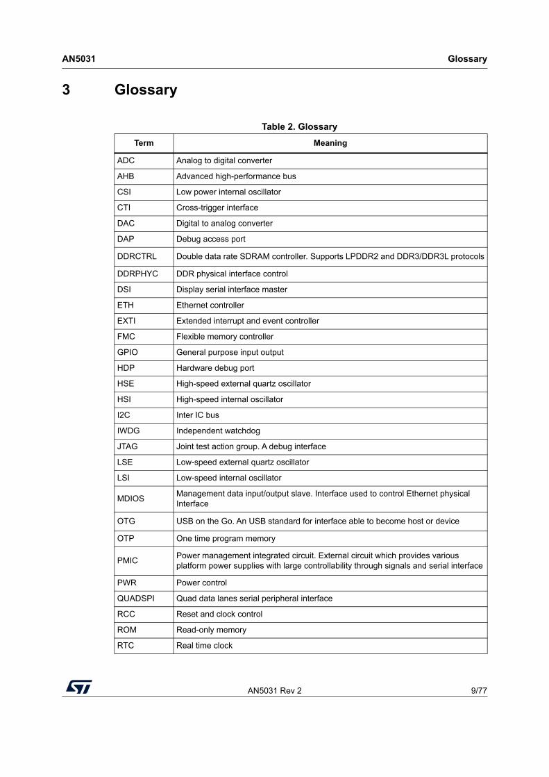
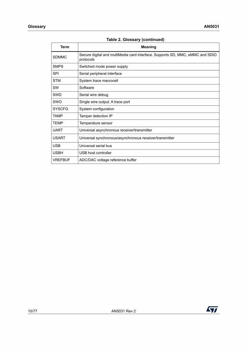
3 Glossary
Table 2. Glossary
Term Meaning
ADC Analog to digital converter
AHB Advanced high-performance bus
CSI Low power internal oscillator
CTI Cross-trigger interface
DAC Digital to analog converter
DAP Debug access port
DDRCTRL Double data rate SDRAM controller. Supports LPDDR2 and DDR3/DDR3L protocols
DDRPHYC DDR physical interface control
DSI Display serial interface master
ETH Ethernet controller
EXTI Extended interrupt and event controller
FMC Flexible memory controller
GPIO General purpose input output
HDP Hardware debug port
HSE High-speed external quartz oscillator
HSI High-speed internal oscillator
I2C Inter IC bus
IWDG Independent watchdog
JTAG Joint test action group. A debug interface
LSE Low-speed external quartz oscillator
LSI Low-speed internal oscillator
MDIOSManagement data input/output slave. Interface used to control Ethernet physical Interface
OTG USB on the Go. An USB standard for interface able to become host or device
OTP One time program memory
PMICPower management integrated circuit. External circuit which provides various platform power supplies with large controllability through signals and serial interface
PWR Power control
QUADSPI Quad data lanes serial peripheral interface
RCC Reset and clock control
ROM Read-only memory
RTC Real time clock
Glossary AN5031
10/77 AN5031 Rev 2
SDMMCSecure digital and multiMedia card interface. Supports SD, MMC, eMMC and SDIO protocols
SMPS Switched mode power supply
SPI Serial peripheral interface
STM System trace macrocell
SW Software
SWD Serial wire debug
SWO Single wire output. A trace port
SYSCFG System configuration
TAMP Tamper detection IP
TEMP Temperature sensor
UART Universal asynchronous receiver/transmitter
USART Universal synchronous/asynchronous receiver/transmitter
USB Universal serial bus
USBH USB host controller
VREFBUF ADC/DAC voltage reference buffer
Table 2. Glossary (continued)
Term Meaning

AN5031 Rev 2 11/77
AN5031 Power supplies
76
4 Power supplies
Figure 1. Power supply scheme
MSv46507V2
BKUP IOs
VDD domain
Analog domain
Core domain
VSW domain
(System logic, Peripherals)
(MPU, peripherals,
RAM)
Leve
l shi
fter
ADC, DAC
(MCU, peripherals,
RAM)
Power switch
VDDCORE
VSS
VBAT
VDDA
VREF+
VREF-
VSSA
Backupregulator
VDD
Backup RAM
Power switch
HSI, CSI, HSE, LSI, WKUP,
IWDG
IOs
DSIregulator
VD
D_D
SI
VD
D1V
2_D
SI_
RE
G
VS
S_D
SI
VSS
VSS
REF_BUF
VSS
IOlogic
VREF+
DSIPLL
VSW
LSE, RTC, AWU, Tamper, backup registers, Reset
IOlogic
VBKP
Retention RAM
Retentionregulator VRET
1V8regulator
VD
DA
1V8_
RE
G
VD
D
VSS
Backup domain
Retention domainVDDIOs
IOlogic
USB FS IOs
VSS
VD
D3V
3_U
SB
FS
USB HS PHY
VD
D3V
3_U
SB
HS
DSI PHY
VD
DA
1V2_
DS
I_P
HY
VD
DA
1V8_
DS
I
VDD_PLL PLLs
DDRPHY
VD
DQ
_DD
R
VSS VSS_DSI
1V1regulator
VSS
VD
DA
1V1_
RE
G
VSS_PLL
VD
D
VS
S_U
SB
HS
VREF-
IOports
IOports
IOports
VDD (VDD_ANA)

Power supplies AN5031
12/77 AN5031 Rev 2
4.1 Introduction
Note: See details and guaranteed operating points in product datasheets.
• The main IOs voltage supply (VDD) range is 1.71 V to 3.6 V.
• The core logic operating voltage supply (VDDCORE) range is 1.18 V to 1.25 V.
• The USB supplies (VDD3V3_USBHS and VDD3V3_USBFS) range is 3.07 V to 3.6 V.
• Embedded regulators are used to supply some internal blocks.
– 1.2 V LDO for DSI available on VDD1V2_DSI_REG which is used to supply DSI PLL and VDD1V2_DSI_PHY pin. Range is 1.15 V to 1.26 V.
– 1.8 V LDO for DSI and USB available on VDDA1V8_REG which is used to supply USB internally and VDDA1V8_DSI. When BYPASS_REG1V8 = VDD, VDDA1V8_REG must be supplied externally. In that case, range is 1.65 V to 1.95 V.
– 1.1 V LDO for USB available on VDD1V1_REG for external decoupling
Note: Embedded regulators must not be used to supply external components.
• The real-time clock (RTC) and backup registers can be powered from the VBAT voltage when the main VDD supply is powered off. This internal supply with automatic switch between VBAT and VDD is named VSW domain and is also used to supply PI8, PC13, PC14, PC15 pads.
VBAT voltage range is 1.20 V to 3.6 V.
When VDD is above VBAT, a small charging current could be enabled on VBAT for an external backup voltage device (for example a supercapacitor).
4.1.1 Independent ADC and DAC converter supply and reference voltage
To improve the conversion accuracy and dynamic range, the ADC, DAC and reference have an independent power supply that can be filtered separately, and shielded from noise on the PCB.
The analog operating voltage supply (VDDA) range is 1.71 V to 3.6 V (DAC could only be used when VDDA is above or equal 1.8 V).
• The ADC/DAC/VREFBUF voltage supply input is available on a separate VDDA pin.
• An isolated supply ground connection is provided on the VSSA pin. In all cases, the VSSA pin should be externally connected to same supply ground than VSS.
External VREF
The user can connect a separate external reference voltage ADC/DAC input on VREF+. The voltage on VREF+ may range from 1.62 V to VDDA.
Note: In order to work, DAC requires VREF+ above 1.8 V.
Internal VREF
The user can enable in the VREFBUF block an internal reference voltage on VREF+. The voltage on VREF+ could be selected between 1.5 V, 1.8 V, 2.048 V and 2.5 V.
With internal VREF available on VREF+ pin, it could be used externally (for example for analog comparator reference) if loading is kept within datasheet values.
Note: In order to work, the DAC requires VREF+ above 1.8 V.
AN5031 Rev 2 13/77
AN5031 Power supplies
76
Note: The VREFBUF requires VDDA equal to or higher than VREF+ + 0.3 V.
Caution: When available (depending on package), VREF– must be externally tied to VSSA.
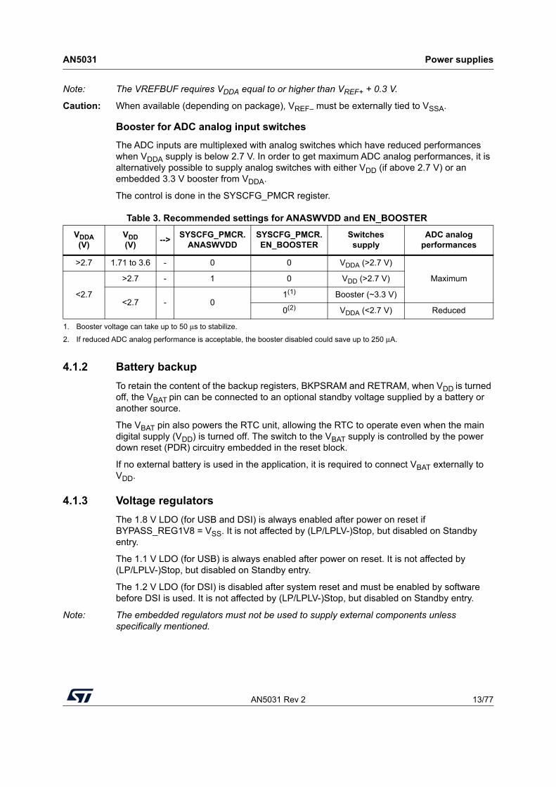
Booster for ADC analog input switches
The ADC inputs are multiplexed with analog switches which have reduced performances when VDDA supply is below 2.7 V. In order to get maximum ADC analog performances, it is alternatively possible to supply analog switches with either VDD (if above 2.7 V) or an embedded 3.3 V booster from VDDA.
The control is done in the SYSCFG_PMCR register.
4.1.2 Battery backup
To retain the content of the backup registers, BKPSRAM and RETRAM, when VDD is turned off, the VBAT pin can be connected to an optional standby voltage supplied by a battery or another source.
The VBAT pin also powers the RTC unit, allowing the RTC to operate even when the main digital supply (VDD) is turned off. The switch to the VBAT supply is controlled by the power down reset (PDR) circuitry embedded in the reset block.
If no external battery is used in the application, it is required to connect VBAT externally to VDD.
4.1.3 Voltage regulators
The 1.8 V LDO (for USB and DSI) is always enabled after power on reset if BYPASS_REG1V8 = VSS. It is not affected by (LP/LPLV-)Stop, but disabled on Standby entry.
The 1.1 V LDO (for USB) is always enabled after power on reset. It is not affected by (LP/LPLV-)Stop, but disabled on Standby entry.
The 1.2 V LDO (for DSI) is disabled after system reset and must be enabled by software before DSI is used. It is not affected by (LP/LPLV-)Stop, but disabled on Standby entry.
Note: The embedded regulators must not be used to supply external components unless specifically mentioned.
Table 3. Recommended settings for ANASWVDD and EN_BOOSTER
VDDA(V)
VDD(V)
-->SYSCFG_PMCR.
ANASWVDDSYSCFG_PMCR.EN_BOOSTER
Switchessupply
ADC analog performances
>2.7 1.71 to 3.6 - 0 0 VDDA (>2.7 V)
Maximum
<2.7
>2.7 - 1 0 VDD (>2.7 V)
<2.7 - 01(1) Booster (~3.3 V)
0(2) VDDA (<2.7 V) Reduced
1. Booster voltage can take up to 50 μs to stabilize.
2. If reduced ADC analog performance is acceptable, the booster disabled could save up to 250 μA.
Power supplies AN5031
14/77 AN5031 Rev 2
4.2 Power supply schemes
The circuit is powered by multiple power supplies:
• The VDD is the main supply for IOs and internal part kept powered during the Standby mode. The useful voltage range is 1.71 V to 3.6 V (for example: 1.8 V, 2.5 V, 3.0 V or 3.3 V typ.)
– Those supplies must be connected to external decoupling capacitors (see Table 4).
– VDD_DSI, VDD_PLL and VDD_ANA must be connected to VDD
• The VDDCORE is the main digital voltage and could be shutdown externally during the Standby mode. The voltage range during Run mode is 1.18 V to 1.25/1.38 V (1.2/1.34 V typ.).
– This supply must be connected to external decoupling capacitors (see Table 4)
– VDDCORE could be reduced further in specific Stop mode (LPLV_Stop). This involves either PWR_ON signal (for example with STPMIC1, external power management IC) or PWR_LP signal (with discrete SMPS components)
• The VBAT pin can be connected to the external battery (1.2 V < VBAT < 3.6 V).
– If RETRAM is used, minimum VBAT is 1.4 V
– If application does not support backup battery, it is recommended to connect this pin to VDD.
– If application is supporting backup battery, it is recommended to add a 100 nF ceramic decoupling capacitor between VBAT and VSS.
– If application is using a supercapacitor on VBAT, no additional decoupling is required.
• The VDDA pin is the analog (ADC/DAC/VREFBUF) supply and must be connected to external decoupling capacitors (see Table 4).
• The VREF+ pin can be connected to the VDDA external power supply. If a separate, internal or external, reference voltage is applied on VREF+, a decoupling capacitor must be connected between this pin and VREF- (see Table 4). Refer to Section 4.1.1.
Additional precautions can be taken to filter analog noise:
– VDDA can be connected to VDD through an inductor based filter.
• VDDQ_DDR is the DDR IO supply and must be connected to external decoupling capacitors (see Table 4).
– Voltage range is 1.425 V to 1.575 V for interfacing DDR3 memories (1.5 V typ.)
– Voltage range is 1.283 V to 1.45 V for interfacing DDR3L memories (1.35 V typ.)
– Voltage range is 1.14 V to 1.3 V for interfacing LPDDR2 or LPDDR3 memories (1.2 V typ.)
• VDDA1V2_DSI_REG pin is the output of internal regulator and must be connected to external decoupling capacitors (see Table 4).
– VDDA1V2_DSI_REG is connected internally to DSI PLL.
• VDDA1V2_DSI_PHY is the analog DSI PHY supply. Voltage range is 1.15 V to 1.26 V. (1.2 V typ.) VDDA1V2_DSI_PHY should be connected to VDDA1V2_DSI_REG.

AN5031 Rev 2 15/77
AN5031 Power supplies
76
• VDD3V3_USBHS and VDD3V3_USBFS are respectively the USB high-speed and full-speed PHY supply. Voltage range is 3.07 V to 3.6 V. Must be connected together to external decoupling capacitors (see Table 4).
VDD3V3_USBFS is used to supply OTG_VBUS and OTG_ID (PA10) pins. So, VDD3V3_USBFS must be supplied as well when USB high-speed dual-role-port or USB high-speed device is used. If not used, should be connected to VDD.
• The VDDA1V8_REG pin is the output of internal regulator and must be connected to external decoupling capacitors (see Table 4).
– VDDA1V8_REG, is connected internally to USB PHY and USB PLL.
– Internal VDDA1V8_REG regulator is enabled by default and could be controlled by software. It is always shutdown during Standby.
For the 1.8 V voltage regulator configuration, there is specific BYPASS_REG1V8 pin that should be connected either to VSS or VDD to activate or deactivate the voltage regulator. It is mandatory to bypass the 1.8 V regulator when VDD is below 2.25 V:
– BYPASS_REG1V8 = VDD. In that case, VDDA1V8_REG pin should be connected to VDD (if below 1.98V) or a dedicated 1.65 V - 1.98 V supply (1.8 V typ.).
– BYPASS_REG1V8 = VSS. In that case, VDD must be above 2.25 V to allow correct behavior of 1.8 V voltage regulator.
– Refer to Section 4.1.3 and section "Embedded regulators characteristics" of the related device datasheet for details.
• VDDA1V8_DSI is the analog DSI supply. the voltage range is 1.65 V to 1.98 V. (1.8 V typ.) Should be connected to VDDA1V8_REG and must be connected to external decoupling capacitors (see Table 4).
• VDDA1V1_REG pin is the output of internal regulator and must be connected to external decoupling capacitors (see Table 4). The voltage range is 1.045 V to 1.155 V (1.1 V typ.)
– VDDA1V1_REG is connected internally to USB PHY.
– Internal VDDA1V1_REG regulator is enabled by default and could be controlled by software. It is always shutdown during Standby.
Caution: VDD3V3_USBHS must not be present unless VDDA1V8_REG is present, otherwise permanent STM32MP15x lines damage could occur. Must be ensured by PMIC ranking order or with external component in case of discrete component power supply implementation.
Caution: All supply grounds (VSS, VSS_ANA, VSS_PLL, VSS_USBHS, VSS_DSI, VSSA and VREF-) should be connected together with power planes.

Power supplies AN5031
16/77 AN5031 Rev 2
Table 4. Amount of decoupling recommendation by package(1)
Supplies pinsDecoupling point(2) Value
LF
BG
A35
4
TF
BG
A25
7
TF
BG
A36
1
LF
BG
A44
8
Comments
VBAT VSS 100 nF 1 1 1 1could be skipped if VBAT is connected to VDD or if a supercapacitor is used instead of a battery
VDDCORE VSS 1 µF(3) 15 15 15 15 Not including capacitors on PMIC/SMPS
VDDQ_DDR VSS
1 nF 2 2 2 2Not including capacitors on PMIC/SMPS and additional capacitors on DDR memory
3.3 nF 0 3 0 0
1 µF(3) 4 2 7 7
VDD_ANA VSS_ANA 1 µF(3) 1 -(4) 1 1 -
VDD_PLL, VDD_PLL2VSS_PLL, VSS_PLL2
1 µF(3) 2 -(4) -(4) 2Not including capacitors on PMIC/SMPS.
VDD, VDD_DSI VSS 1 µF(3) 4 4 4 4
VDD1V2_DSI_REG, VDD1V2_DSI_PHY
VSS_DSI2.2 µF(3)
1 - 1 1-
VSS - 1(5) - -
VDDA1V8_REG
VSS_USBHS2.2 µF(3)
1 - 1 1-
VSS - 1(5) - -
VDDA1V8_DSI
VSS_DSI1 µF(3)
1 - 1 1 VDDA1V8_DSI must be connected to VDDA1V8_REGVSS - 1(5) - -
VDDA1V1_REG
VSS_USBHS2.2 µF(3)
1 - 1 1-
VSS - 1(5) - -
VDD3V3_USBHS, VDD3V3_USBFS
VSS_USBHS1 µF(3)
1 - 1 1-
VDD3V3_USB VSS - 1(5) - -
VDDA VSSA100 nF + 1 µF(3) 1+1 1+1 1+1 1+1 VSSA must be connected to VSS plane
VREF+
VREF- and VSSA 100 nF +
1 µF(3)
1+1 - - 1+1VREF- must be connected to VSSA then VSS plane
VSSA -1+1(6)
1+1(6) - VSSA must be connected to VSS plane
1. This table could be used as a guideline, the real count and values of capacitors could be adapted depending of various parameters: capacitor size, capacitor dielectric, PCB technology, and using results of product power integrity simulations.
2. All VSS_x and VSSA must be connected to a common VSS plane.
3. Multi Layer Ceramic Capacitor type (MLCC).
4. Supply internally merged with VDD.
5. Supply return path internally merged with VSS.
6. VREF- internally merged with VSSA.
AN5031 Rev 2 17/77
AN5031 Power supplies
76
4.3 Reset and power supply supervisor
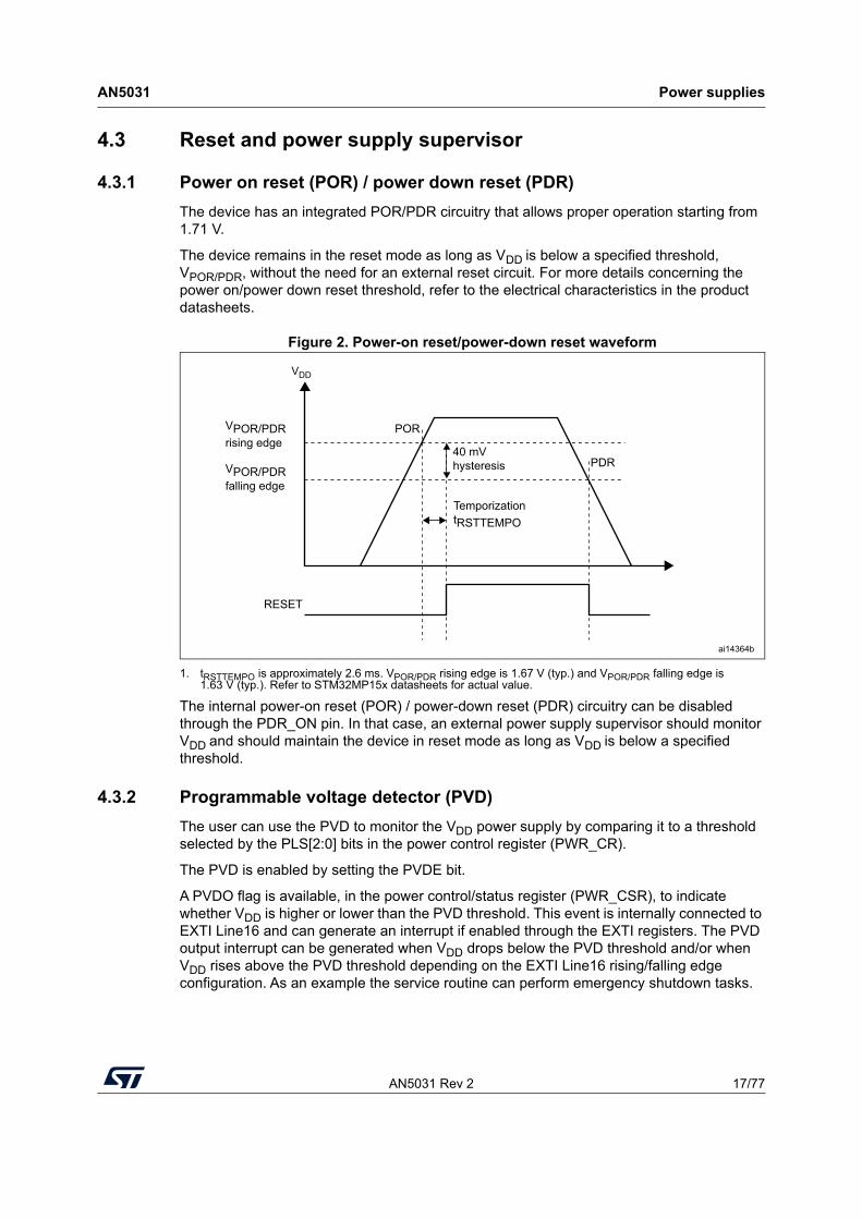
4.3.1 Power on reset (POR) / power down reset (PDR)
The device has an integrated POR/PDR circuitry that allows proper operation starting from 1.71 V.
The device remains in the reset mode as long as VDD is below a specified threshold, VPOR/PDR, without the need for an external reset circuit. For more details concerning the power on/power down reset threshold, refer to the electrical characteristics in the product datasheets.
Figure 2. Power-on reset/power-down reset waveform
1. tRSTTEMPO is approximately 2.6 ms. VPOR/PDR rising edge is 1.67 V (typ.) and VPOR/PDR falling edge is 1.63 V (typ.). Refer to STM32MP15x datasheets for actual value.
The internal power-on reset (POR) / power-down reset (PDR) circuitry can be disabled through the PDR_ON pin. In that case, an external power supply supervisor should monitor VDD and should maintain the device in reset mode as long as VDD is below a specified threshold.
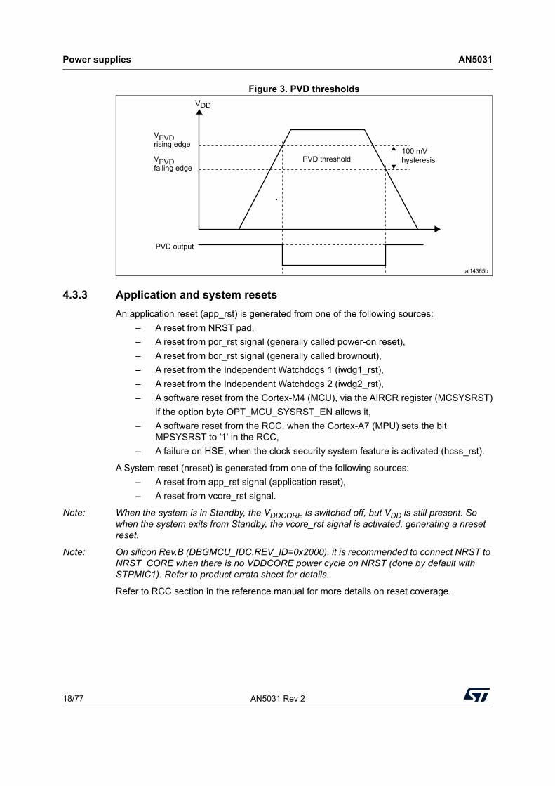
4.3.2 Programmable voltage detector (PVD)
The user can use the PVD to monitor the VDD power supply by comparing it to a threshold selected by the PLS[2:0] bits in the power control register (PWR_CR).
The PVD is enabled by setting the PVDE bit.
A PVDO flag is available, in the power control/status register (PWR_CSR), to indicate whether VDD is higher or lower than the PVD threshold. This event is internally connected to EXTI Line16 and can generate an interrupt if enabled through the EXTI registers. The PVD output interrupt can be generated when VDD drops below the PVD threshold and/or when VDD rises above the PVD threshold depending on the EXTI Line16 rising/falling edge configuration. As an example the service routine can perform emergency shutdown tasks.
VDD
POR
PDR40 mVhysteresis
TemporizationtRSTTEMPO
RESET
ai14364b
VPOR/PDRfalling edge
VPOR/PDRrising edge
Power supplies AN5031
18/77 AN5031 Rev 2
Figure 3. PVD thresholds
4.3.3 Application and system resets
An application reset (app_rst) is generated from one of the following sources:
– A reset from NRST pad,
– A reset from por_rst signal (generally called power-on reset),
– A reset from bor_rst signal (generally called brownout),
– A reset from the Independent Watchdogs 1 (iwdg1_rst),
– A reset from the Independent Watchdogs 2 (iwdg2_rst),
– A software reset from the Cortex-M4 (MCU), via the AIRCR register (MCSYSRST)
if the option byte OPT_MCU_SYSRST_EN allows it,
– A software reset from the RCC, when the Cortex-A7 (MPU) sets the bit MPSYSRST to '1' in the RCC,
– A failure on HSE, when the clock security system feature is activated (hcss_rst).
A System reset (nreset) is generated from one of the following sources:
– A reset from app_rst signal (application reset),
– A reset from vcore_rst signal.
Note: When the system is in Standby, the VDDCORE is switched off, but VDD is still present. So when the system exits from Standby, the vcore_rst signal is activated, generating a nreset reset.
Note: On silicon Rev.B (DBGMCU_IDC.REV_ID=0x2000), it is recommended to connect NRST to NRST_CORE when there is no VDDCORE power cycle on NRST (done by default with STPMIC1). Refer to product errata sheet for details.
Refer to RCC section in the reference manual for more details on reset coverage.
VDD
100 mVhysteresisPVD threshold
PVD output
ai14365b
VPVDfalling edge
VPVDrising edge

AN5031 Rev 2 19/77
AN5031 Power supplies
76
Figure 4. Simplified reset pin circuit
RP
U
10 nF
FilterNRST
HSECSS resetIWDG1/2 resetsSoftware resets
Pulse generator
(min 20 μs)
optional reset circuit
To/from other components
VDD
RP
U
10 nF
FilterNRST_COREFrom other
components
System reset(nreset)(logic on VDDCORE)
Application reset(app_rst)
MSv48327V2
VDD
VDD
VDDPWR (BOR) reset
PDR_ON
VDDVDD
PDR_ON
PORPDR
VDD
BORVDD
PWR (POR/PDR) reset
PDR_ON_CORE
VDDVDD
PORPDR PWR (VDDCORE OK)
reset
VDDCORE
PDR_ON_CORE
optional reset circuit
On silicon Rev.B, recommended connection when there is no
VDDCORE power cycle on NRST (done by default with STPMIC1)
(1) : capacitor could be removed if NRST_CORE is connected to NRST
(1)

Packages AN5031
20/77 AN5031 Rev 2
5 Packages
5.1 Package selection
The package must be selected by taking into account the constraints that are strongly dependent upon the application.
The list below summarizes the more frequent constraints:
– Amount of interfaces required. Some interfaces might not be available on some packages. Some interfaces combinations might not be possible on some packages. Refer to product datasheets for details
– PCB technology constraints. Small pitch and high ball density could require more PCB layers and higher PCB class requiring stackup with micro-via (laser via) technology
– Package height
– PCB available area
– Thermal constraints (larger packages have better thermal dissipation capabilities)
Table 5. Package summary
Size (mm)(1)
1. Typical body size.
16 x 16 10 x 10 12 x 12 18 x 18
Minimum Pitch (mm) 0.8 0.5 0.5 0.8
Height (mm) 1.4 1.2 1.2 1.4
Sales numbers LFBGA354 TFBGA257 TFBGA361 LFBGA448
STM32MP151xxx X X X X
STM32MP153xxx X X X X
STM32MP157xxx X X X X
AN5031 Rev 2 21/77
AN5031 Packages
76
Table 6. Major feature changes related to packages
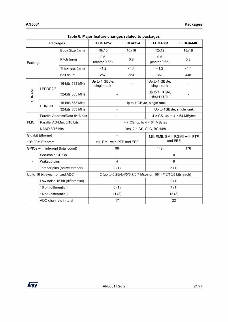
Packages TFBGA257 LFBGA354 TFBGA361 LFBGA448
Package
Body Size (mm) 10x10 16x16 12x12 18x18
Pitch (mm)0.5
(center 0.65)0.8
0.5
(center 0.65)0.8
Thickness (mm) <1.2 <1.4 <1.2 <1.4
Ball count 257 354 361 448
SD
RA
M
LPDDR2/3
16-bits 533 MHzUp to 1 GByte,
single rank -
Up to 1 GByte, single rank
-
32-bits 533 MHz -Up to 1 GByte,
single rank -
DDR3/3L 16-bits 533 MHz Up to 1 GByte, single rank
32-bits 533 MHz - Up to 1GByte, single rank
FMC
Parallel Address/Data 8/16 bits - 4 × CS, up to 4 × 64 MBytes
Parallel AD-Mux 8/16 bits 4 × CS, up to 4 × 64 MBytes
NAND 8/16 bits Yes, 2 × CS, SLC, BCH4/8
Gigabit Ethernet - MII, RMII, GMII, RGMII with PTP and EEE10/100M Ethernet MII, RMII with PTP and EEE
GPIOs with interrupt (total count) 98 148 176
-
Securable GPIOs - 8
Wakeup pins 4 6
Tamper pins (active tamper) 2 (1) 3 (1)
Up to 16 bit synchronized ADC 2 (up to 0.25/4.4/5/5.7/6.7 Msps on 16/14/12/10/8 bits each)
-
Low noise 16 bit (differential) - 2 (1)
16 bit (differential) 6 (1) 7 (1)
14 bit (differential) 11 (3) 13 (3)
ADC channels in total 17 22
Packages AN5031
22/77 AN5031 Rev 2
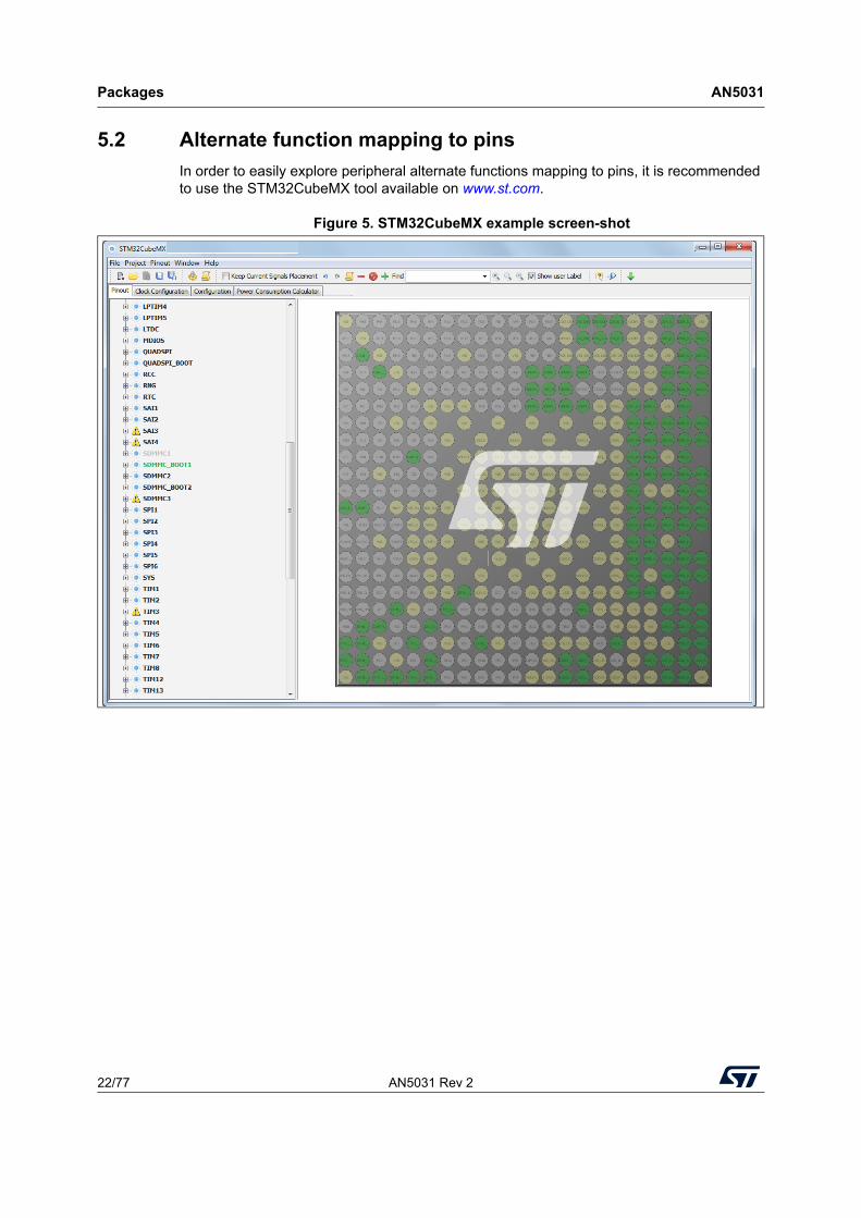
5.2 Alternate function mapping to pins
In order to easily explore peripheral alternate functions mapping to pins, it is recommended to use the STM32CubeMX tool available on www.st.com.
Figure 5. STM32CubeMX example screen-shot
AN5031 Rev 2 23/77
AN5031 Packages
76
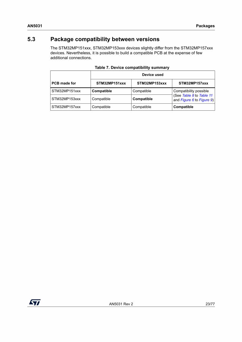
5.3 Package compatibility between versions
The STM32MP151xxx, STM32MP153xxx devices slightly differ from the STM32MP157xxx devices. Nevertheless, it is possible to build a compatible PCB at the expense of few additional connections.
Table 7. Device compatibility summary
PCB made for
Device used
STM32MP151xxx STM32MP153xxx STM32MP157xxx
STM32MP151xxx Compatible Compatible Compatibility possible (See Table 8 to Table 11 and Figure 6 to Figure 9)STM32MP153xxx Compatible Compatible
STM32MP157xxx Compatible Compatible Compatible

Packages AN5031
24/77 AN5031 Rev 2
Figure 6. 16x16 LFBGA354 compatibility
Note: This drawing is to help understanding and does not show realistic board traces and components size/placement.
Table 8. STM32MP151xxx and STM32MP153xxx for 16x16 LFBGA354 compatibility
Ball connection to add STM32MP151xxx STM32MP153xxx STM32MP157xxx
B12 to V11 (VDD1V8_REG) VDDA1V8_Unused VDDA1V8_DSI
A16 to B16 + 1 µF to VSS VDD1V2_UnusedVDD1V2_DSI_PHY / VDD1V2_DSI_REG
A12 to VDD VDD_Unused VDD_DSI
2.2uF
PC11VDD_Unuse
d
11 12
A
B
C
D
E
PE4
PC8
PC10 NJTRST
VDDCORE VSS
DNU
13
DNU
JTDI
VDDCORE
14 15 16 17 18 19
DNU DNUVDD1V2_Unused
DDR_DQ0
DDR_DQ1 VSS
DNU DNU DDR_DQ3
DDR_DQ7
DDR_DQS0
N
DDR_DQM0
DDR_DQS0
PJTDO-TRACESWO
JTMS-SWDI
O
JTCK-SWCL
K
DDR_DQ5
VSS
DDR_DQ2
DDR_DQ6
DDR_DQ4VSS DDR_
A7VSS VDDQ_DDR
PC11 VDD_DSI
11 12
PE4
PC8 VSS_DSI
PC10 NJTRST
VDDCORE VSS
DSI_D0_N
13
DSI_D0_P
JTDI
VDDCORE
14 15 16 17 18 19
DSI_CK_N
DSI_D1_N
VDD1V2_DSI_PH
Y
DDR_DQ0
DDR_DQ1 VSS
DSI_CK_P
DSI_D1_P
VDD1V2_DSI_RE
G
DDR_DQ3
DDR_DQ7
DDR_DQS0
N
VSS_DSI
VSS_DSI
DDR_DQM0
DDR_DQS0
PJTDO-TRACESWO
JTMS-SWDI
O
JTCK-SWCL
K
DDR_DQ5
VSS_DSI
DDR_DQ2
DDR_DQ6
DDR_DQ4VSS DDR_
A7VSS VDDQ_DDR
A
B
C
D
E
VSS VDDCORE
VSS
VSS
VDDCORE VSS
VSS VDDCORE
VDDCORE VSS
VSS VDDCORE
VSS_PLL2
VSS
VDDCORE
VSS
VDDCORE
VSS
VDDCORE VSS VDDC
ORE
VSS
PE8
PD12
VDDA1V8_R
EGVDDA1V1_R
EG
VDDCORE
VSS
PD13
VSS_USBH
SVDD3V3_USBHS
VSS
PB2
VSS_USBH
S
USB_DM2
USB_DP2
VDDQ_DDR
VSS
VSS_USBH
S
USB_DP1
USB_DM1
VSS
BYPASS_REG1V
8OTG_VBUS
VSS_USBH
SVDD3V3_USBFS
VSS
PA12
USB_RREF
DDR_VREF
DDR_A4
DDR_A8
DDR_DQ9
VSS
PA11
DDR_DQ15
DDR_DQ8
DDR_DQ10
DDR_DQ13
DDR_DQM1
DDR_DQ14
DDR_DQ12
DDR_CKE
DDR_DQS1
NDDR_DQS1
P
DDR_DQ11
VSS
VDDQ_DDR VSS DDR_
DTO0DDR_CLKN
VSS DDR_A15
DDR_A12
DDR_RASN
DDR_CLKP
VDDQ_DDR VSS DDR_
A1DDR_A11
DDR_A10
DDR_ZQ
DDR_A3
DDR_A13
VDDQ_DDR VSS
DDR_A2
DDR_BA0
DDR_RESE
TN
DDR_A9VSS
DDR_A0
DDR_ODT
DDR_A5
DDR_CSN
DDR_DTO1
DDR_BA2
DDR_WENVSS
DDR_CASN
VSS DDR_A6
DDR_BA1
DDR_A14
DDR_ATO
VSS
VDDCORE
VDD_PLL2
VDDQ_DDR
VDDCORE
VDDQ_DDR
VDDQ_DDR
VDDQ_DDR
VDDQ_DDR
VDD VDDCORE
VDDQ_DDR
PB6 PG9 PA10
F
G
H
J
K
L
M
N
P
R
T
U
V
W
VSS VDDCORE
VSS
VSS
VDDCORE VSS
VSS VDDCORE
VDDCORE VSS
VSS VDDCORE
VSS_PLL2
VSS
VDDCORE
VSS
VDDCORE
VSS
VDDCORE VSS VDDC
ORE
VSS
PE8
PD12
VDDA1V8_R
EGVDDA1V1_R
EG
VDDCORE
VSS
PD13
VSS_USBH
SVDD3V3_USBHS
VSS
PB2
VSS_USBH
S
USB_DM2
USB_DP2
VDDQ_DDR
VSS
VSS_USBH
S
USB_DP1
USB_DM1
VSS
BYPASS_REG1V
8OTG_VBUS
VSS_USBH
SVDD3V3_USBFS
VSS
PA12
USB_RREF
DDR_VREF
DDR_A4
DDR_A8
DDR_DQ9
VSS
PA11
DDR_DQ15
DDR_DQ8
DDR_DQ10
DDR_DQ13
DDR_DQM1
DDR_DQ14
DDR_DQ12
DDR_CKE
DDR_DQS1
NDDR_DQS1
P
DDR_DQ11
VSS
VDDQ_DDR VSS DDR_
DTO0DDR_CLKN
VSS DDR_A15
DDR_A12
DDR_RASN
DDR_CLKP
VDDQ_DDR VSS DDR_
A1DDR_A11
DDR_A10
DDR_ZQ
DDR_A3
DDR_A13
VDDQ_DDR VSS
DDR_A2
DDR_BA0
DDR_RESE
TN
DDR_A9VSS
DDR_A0
DDR_ODT
DDR_A5
DDR_CSN
DDR_DTO1
DDR_BA2
DDR_WENVSS
DDR_CASN
VSS DDR_A6
DDR_BA1
DDR_A14
DDR_ATO
VSS
VDDCORE
VDD_PLL2
VDDQ_DDR
VDDCORE
VDDQ_DDR
VDDQ_DDR
VDDQ_DDR
VDDQ_DDR
VDD VDDCORE
VDDQ_DDR
PB6 PG9 PA10
F
G
H
J
K
L
M
N
P
R
T
U
V
W
VSS
2.2uF
VSS VSS VSS VSSC
onne
ct.
Con
nect
.
STM32MP151xxx with compatibilitySTM32MP153xxx with compatibility STM32MP157xxx
Con
nect
. C
onne
ct.
1uF
VDDA1V8_Unused
VDD1V2_Unused
VSSVSS
1uF
VDDA1V8_D
SI
VSS_DSI
MSv48308V2VDD VDDA1V8 VDD1V2 VSS
AN5031 Rev 2 25/77
AN5031 Packages
76
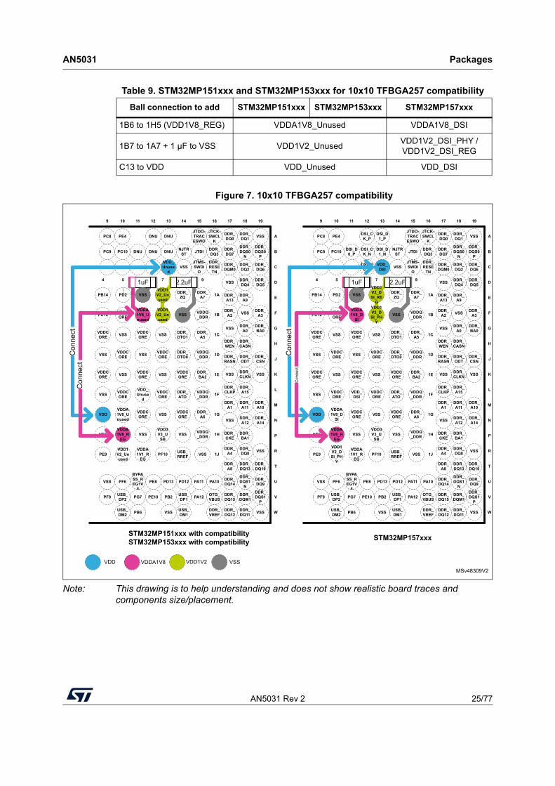
Figure 7. 10x10 TFBGA257 compatibility
Note: This drawing is to help understanding and does not show realistic board traces and components size/placement.
Table 9. STM32MP151xxx and STM32MP153xxx for 10x10 TFBGA257 compatibility
Ball connection to add STM32MP151xxx STM32MP153xxx STM32MP157xxx
1B6 to 1H5 (VDD1V8_REG) VDDA1V8_Unused VDDA1V8_DSI
1B7 to 1A7 + 1 µF to VSS VDD1V2_UnusedVDD1V2_DSI_PHY / VDD1V2_DSI_REG
C13 to VDD VDD_Unused VDD_DSI
DDR_ZQ
2.2uF
PC8 PE4 DSI_CK_P
9 10 11 12
A
B
C
D
E
F
G
H
J
K
L
M
PC9 PC10 DSI_D0_P
DSI_CK_N
PB9 PC7 PC11 DSI_D0_N
DSI_D1_P
13
DSI_D1_N
VDD_DSI
N
14 15 16 17 18 19
P
R
T
U
V
W
VSS
PF9
PF6
USB_DP2
USB_DM2
BYPASS_REG1V
8
PG7
PB6
PE8
PE10
PD13
PB2
VSS
PD12
USB_DP1
USB_DM1
PA11
PA12
PA10
OTG_VBUS
DDR_VREF
DDR_CKE
DDR_A4
DDR_A8
DDR_DQ14
DDR_DQ15
DDR_DQ12
DDR_BA1
DDR_DQ8
DDR_DQ13
DDR_DQS1
N
DDR_DQM1
DDR_DQ11
DDR_DQ10
DDR_DQ9
DDR_DQS1
P
VSS
JTDO-TRACESWO
JTCK-SWCL
K
DDR_DQ0
DDR_DQ1 VSS
NJTRST JTDI DDR_
DQ3DDR_DQ7
DDR_DQS0
N
DDR_DQS0
P
VSSJTMS-SWDI
O
DDR_DQ2
DDR_DQ6
DDR_CLKN VSS
DDR_CLKP
DDR_A15
DDR_A1
DDR_A11
DDR_A10
VSS
DDR_RESE
TN
DDR_DQM0
DDR_DQ4
DDR_DQ5
DDR_A9
DDR_A13
VSS DDR_A3
DDR_A2
DDR_A0
DDR_BA0VSS
DDR_CASN
DDR_WEN
DDR_ODT
DDR_CSN
DDR_RASN
VSS
VSS DDR_A12
DDR_A14
PB14 PD2
VDD1V2_DSI_RE
G
4 5 6 7 9
1A
1B
1C
1D
1E
1F
1G
1H
1J
PC12 VDDCORE
VDD1V2_DSI_PH
Y
VSS VDDQ_DDR
VDDCORE VSS DDR_
DTO1DDR_
A5
VSS VDDCORE VSS VDDC
ORE
VDDCORE VSS
DDR_DTO0
VDDQ_DDR
VDDCORE
VSS
VDD
VSS
PE9
VSS
VDDCORE
VDDA1V8_D
SI
VDDA1V8_R
EG
VDD1V2_DSI_PH
Y
VDDCORE
VDD_DSI
VDDCORE
VSS
VDDA1V1_R
EG
VSS
VDDCORE
VSS
VDD3V3_USB
PF10
VDDCORE
DDR_ATO
VDDCORE
VSS
USB_RREF
DDR_BA2
VDDQ_DDR
DDR_A6
VDDQ_DDR
VSS
DDR_A7
VSS
PC8 PE4 DNU
9 10 11 12
PC9 PC10 DNU DNU
PB9 PC7 PC11 DNU
DNU
13
DNU
VDD_Unuse
d
14 15 16 17 18 19
VSS
PF9
PF6
USB_DP2
USB_DM2
BYPASS_REG1V
8
PG7
PB6
PE8
PE10
PD13
PB2
VSS
PD12
USB_DP1
USB_DM1
PA11
PA12
PA10
OTG_VBUS
DDR_VREF
DDR_CKE
DDR_A4
DDR_A8
DDR_DQ14
DDR_DQ15
DDR_DQ12
DDR_BA1
DDR_DQ8
DDR_DQ13
DDR_DQS1
N
DDR_DQM1
DDR_DQ11
DDR_DQ10
DDR_DQ9
DDR_DQS1
P
VSS
JTDO-TRACESWO
JTCK-SWCL
K
DDR_DQ0
DDR_DQ1 VSS
NJTRST JTDI DDR_
DQ3DDR_DQ7
DDR_DQS0
N
DDR_DQS0
P
VSSJTMS-SWDI
O
DDR_DQ2
DDR_DQ6
DDR_CLKN VSS
DDR_CLKP
DDR_A15
DDR_A1
DDR_A11
DDR_A10
VSS
DDR_RESE
TN
DDR_DQM0
DDR_DQ4
DDR_DQ5
DDR_A9
DDR_A13
VSS DDR_A3
DDR_A2
DDR_A0
DDR_BA0VSS
DDR_CASN
DDR_WEN
DDR_ODT
DDR_CSN
DDR_RASN
VSS
VSS DDR_A12
DDR_A14
PB14 PD2VDD1V2_Unused
DDR_ZQ
4 5 6 7 8 9
PC12 VDDCORE
VDD1V2_Unused
VSS VDDQ_DDR
VDDCORE VSS DDR_
DTO1DDR_
A5
VSS VDDCORE VSS VDDC
ORE
VDDCORE VSS
DDR_DTO0
VDDQ_DDR
VDDCORE
VSS
VDD
VSS
PE9
VSS
VDDCORE
VDDA1V8_Unused
VDDA1V8_R
EG
VDD1V2_Unused
VDDCORE
VDD_Unuse
d
VDDCORE
VSS
VDDA1V1_R
EG
VSS
VDDCORE
VSS
VDD3V3_USB
PF10
VDDCORE
DDR_ATO
VDDCORE
VSS
USB_RREF
DDR_BA2
VDDQ_DDR
DDR_A6
VDDQ_DDR
VSS
DDR_A7
VSS
A
B
C
D
E
F
G
H
J
K
L
M
N
P
R
T
U
V
W
1A
1B
1C
1D
1E
1F
1G
1H
1J
STM32MP151xxx with compatibilitySTM32MP153xxx with compatibility STM32MP157xxx
2.2uFC
onne
ct.
Con
nect
.
Con
nect
. C
onne
ct.
1uF
VSS
VDDA1V8_Unused
1uF
VDDA1V8_D
SI
VSS
MSv48309V2VDD VDDA1V8 VDD1V2 VSS
Packages AN5031
26/77 AN5031 Rev 2
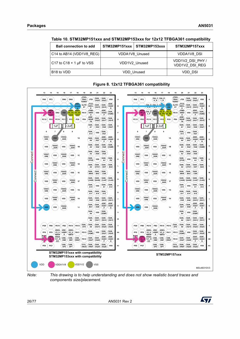
Figure 8. 12x12 TFBGA361 compatibility
Note: This drawing is to help understanding and does not show realistic board traces and components size/placement.
Table 10. STM32MP151xxx and STM32MP153xxx for 12x12 TFBGA361 compatibility
Ball connection to add STM32MP151xxx STM32MP153xxx STM32MP157xxx
C14 to AB14 (VDD1V8_REG) VDDA1V8_Unused VDDA1V8_DSI
C17 to C18 + 1 µF to VSS VDD1V2_UnusedVDD1V2_DSI_PHY / VDD1V2_DSI_REG
B18 to VDD VDD_Unused VDD_DSI
PC11
A
B
C
D
E
F
G
H
J
K
L
M
PA8
13
PB4
PB14
PC12
N
14 15 16 17 18 19 20 21 22
P
R
T
U
V
W
Y
AA
AB
PG9
PF6
BYPASS_REG1V
8
PB6
PF9
VDDA1V8_R
EG
PE10
VDD3V3_USBHSVDDA1V1_R
EG
PB2
VSS_USBH
S
USB_DM2
PA10
VDD3V3_USBFS
USB_DM1
PD12
PA11
USB_RREF
DDR_ATO
PD13
PA12
DDR_A15
DDR_A11
DDR_CKE
DDR_BA1
DDR_A4
DDR_A6
DDR_A8
DDR_DQM3
DDR_DQ27
VSS
DDR_A14
DDR_DQ8
DDR_DQ9
VSS
DDR_DQ11
DDR_DQ15
VSS
DDR_DQ26
DDR_A10
DDR_DQ10
DDR_DQM1
DDR_DQ14
DDR_DQ25
DDR_DQ31
DDR_DQS3
P
PF2 DNU DNUJTDO-TRACESWO
JTDI DDR_DQ20
DDR_DQ23
PC6 DNU DNU DNUVDD_Unuse
d
NJTRST
JTCK-SWCL
K
DDR_DQ19
DDR_DQ16
DNUVDD1V2_Unused
PA15JTMS-SWDI
OVSS
DDR_DQS2
PDDR_RESE
TN
DDR_DQ22
DDR_DQ17
DDR_A7
DDR_DQ3
DDR_DQ0
VSS
DDR_DQ7
DDR_DQS0
P
DDR_A5
DDR_DQ2
DDR_DQ6
DDR_A2
DDR_DQ4
DDR_DTO0 VSS DDR_
A3
DDR_A0
DDR_DTO1
DDR_ODT
DDR_WEN
DDR_BA2
DDR_CSN
PD3 PC10 PC9
VSS
PC8 PE4
DDR_A13
DDR_A9
DDR_CASN
DDR_RASN
DDR_CLKP
23
DDR_A12
DDR_DQ13
DDR_DQS1
N
DDR_DQ12
DDR_DQ24
DDR_DQ30
DDR_DQS3
N
VSS
DDR_DQS2
N
DDR_DQM2
DDR_DQ18
DDR_DQ21
DDR_DQS0
N
DDR_DQM0
DDR_ZQ
DDR_BA0
DDR_CLKN
DDR_DQS1
P
DDR_A1
DDR_DQ5
DDR_DQ1
ACPE8 PG7 USB_DP2
USB_DP1
OTG_VBUS
DDR_VREF
DDR_DQ29
DDR_DQ28 VSS
VDDCORE VSS VDDQ
_DDR
6 7 8 9
1A
1B
1C
1D
1E
1F
1G
1H
1J
VSS VDDQ_DDR VSS VDDQ
_DDR
VDDQ_DDR VSS
VSS VDDCORE
VDDCORE VSS
VSS VDDQ_DDR
VDDCORE
VSS
VDDCORE
VSS
VDD
VSS
VDDCORE
VSS
VDDCORE
VSS
VDDQ_DDR
VSS
VDDQ_DDR
VSS
VDDQ_DDR
VSS
VDDQ_DDR
VSS
VDDQ_DDR
PA8
13
PB4
PB14
PC12
14 15 16 17 18 19 20 21 22
PG9
PF6
BYPASS_REG1V
8
PB6
PF9
VDDA1V8_R
EG
PE10
VDD3V3_USBHSVDDA1V1_R
EG
PB2
VSS_USBH
S
USB_DM2
PA10
VDD3V3_USBFS
USB_DM1
PD12
PA11
USB_RREF
DDR_ATO
PD13
PA12
DDR_A15
DDR_A11
DDR_CKE
DDR_BA1
DDR_A4
DDR_A6
DDR_A8
DDR_DQM3
DDR_DQ27
VSS
DDR_A14
DDR_DQ8
DDR_DQ9
VSS
DDR_DQ11
DDR_DQ15
VSS
DDR_DQ26
DDR_A10
DDR_DQ10
DDR_DQM1
DDR_DQ14
DDR_DQ25
DDR_DQ31
DDR_DQS3
P
PF2 DSI_CK_N
DSI_D1_N
JTDO-TRACESWO
JTDI DDR_DQ20
DDR_DQ23
PC6 DSI_D0_N
DSI_CK_P
DSI_D1_P
VDD_DSI
NJTRST
JTCK-SWCL
K
DDR_DQ19
DDR_DQ16
DSI_D0_P
VDD1V2_DSI_RE
G
PA15JTMS-SWDI
OVSS
DDR_DQS2
PDDR_RESE
TN
DDR_DQ22
DDR_DQ17
DDR_A7
DDR_DQ3
DDR_DQ0
VSS
DDR_DQ7
DDR_DQS0
P
DDR_A5
DDR_DQ2
DDR_DQ6
DDR_A2
DDR_DQ4
DDR_DTO0 VSS DDR_
A3
DDR_A0
DDR_DTO1
DDR_ODT
DDR_WEN
DDR_BA2
DDR_CSN
PD3 PC10 PC11 PC9 PC8 PE4
DDR_A13
DDR_A9
DDR_CASN
DDR_RASN
DDR_CLKP
23
DDR_A12
DDR_DQ13
DDR_DQS1
N
DDR_DQ12
DDR_DQ24
DDR_DQ30
DDR_DQS3
N
VSS
DDR_DQS2
N
DDR_DQM2
DDR_DQ18
DDR_DQ21
DDR_DQS0
N
DDR_DQM0
DDR_ZQ
DDR_BA0
DDR_CLKN
DDR_DQS1
P
DDR_A1
DDR_DQ5
DDR_DQ1
PE8 PG7 USB_DP2
USB_DP1
OTG_VBUS
DDR_VREF
DDR_DQ29
DDR_DQ28 VSS
VDDCORE
VDDQ_DDR
6 7 8 9
VSS VDDQ_DDR VSS VDDQ
_DDR
VDDQ_DDR VSS
VSS VDDCORE
VDDCORE VSS
VSS VDDQ_DDR
VDDCORE
VSS
VDDCORE
VSS
VDD
VSS
VDDCORE
VSS
VDDCORE
VSS
VDDQ_DDR
VSS
VDDQ_DDR
VSS
VDDQ_DDR
VSS
VDDQ_DDR
VSS
VDDQ_DDR
A
B
C
D
E
F
G
H
J
K
L
M
N
P
R
T
U
V
W
Y
AA
AB
AC
1A
1B
1C
1D
1E
1F
1G
1H
1J
STM32MP151xxx with compatibilitySTM32MP153xxx with compatibility STM32MP157xxx
Con
nect
. C
onne
ct.
Con
nect
. C
onne
ct.
2.2uF 2.2uF
VDD1V2_Unused
VDD1V2_DSI_PH
Y
1uF
VDDA1V8_Unused
1uF
VDDA1V8_D
SI
VSS_DSI
VSS
MSv48310V3VDD VDDA1V8 VDD1V2 VSS

AN5031 Rev 2 27/77
AN5031 Packages
76
Figure 9. 18x18 LFBGA448 compatibility
Note: This drawing is to help understanding and does not show realistic board traces and components size/placement.
Table 11. STM32MP151xxx and STM32MP153xxx for 18x18 LFBGA448 compatibility
Ball connection to add STM32MP151xxx STM32MP153xxx STM32MP157xxx
B14 to AB12 (VDD1V8_REG) VDDA1V8_Unused VDDA1V8_DSI
A18 to B18 + 1 µF to VSS VDD1V2_UnusedVDD1V2_DSI_PHY / VDD1V2_DSI_REG
A14 to VDD VDD_Unused VDD_DSI
STM32MP151xxx with compatibilitySTM32MP153xxx with compatibility STM32MP157xxx
PB3
12
A
B
C
D
E
F
G
H
J
K
L
M
PB15
PE5
PD2
PC12
PB9
VSS
VDDCORE
VSS
VDDCORE
VSS
PB14
13
PA8
PB4
PC7
PC6
PF2
VDDCORE
VSS
VDDCORE
VSS
VDDCORE
NVDDCORE VSS
14 15 16 17 18 19 20 21 22
P
R
T
U
V
W
Y
AA
AB
VSS
VDD
VDD
PF10
PD12
PE8
BYPASS_REG1V
8VDDA1V8_R
EG
VDDCORE
VDD
VSS
PB2
PB6
VSS_USBH
SVSS_USBH
SVDD3V3_USBHS
VSS
VDDCORE
VDD
PD13
PE10
VSS_USBH
S
USB_DM2
USB_DP2
VDDCORE
VDDCORE
VSS
OTG_VBUS
PG9
VSS_USBH
S
USB_DP1
USB_DM1
VDDQ_DDR
VDDQ_DDR
VSS
PA12
PA11
VSS_USBH
SVDD3V3_USBFS
VDDQ_DDR
VSS
VDDQ_DDR
VSS
VDDQ_DDR
VSS
PA10
USB_RREF
VDDA1V1_R
EG
DDR_A14
DDR_BA1
DDR_A4
DDR_A8
VSS
VDDQ_DDR
VSS
VSS
VSS
DDR_A11
DDR_CKE
VSS
DDR_A6
VSS
VSS
VDDQ_DDR
DDR_ATO
DDR_VREF
VSS
DDR_DQ13
DDR_DQ11
VSS
DDR_DQ12
DDR_DQ25
VSS
DDR_DQ29
DDR_DQ27
DDR_DQ10
DDR_DQ9
DDR_DQM1
DDR_DQ14
DDR_DQ15
DDR_DQ31
DDR_DQS3
P
DDR_DQ28
DDR_DQ26
DDR_DQS1
NDDR_DQS1
P
DDR_DQ24
DDR_DQ30
DDR_DQS3
N
DDR_DQM3
VSS
VDD_DSI
DSI_D0_N
DSI_CK_N
DSI_D1_N
DDR_DQ20
DDR_DQ23 VSS
VDDA1V8_D
SI
DSI_D0_P
DSI_CK_P
DSI_D1_P
DDR_DQ19
DDR_DQ16
DDR_DQS2
N
VSS_DSI
VSS_DSI
VSS_DSI VSS VSS
DDR_DQS2
P
DDR_DQM2
DDR_DQ22
DDR_DQ17
DDR_DQ18
DDR_DQ3
DDR_DQ0
DDR_DQ21
DDR_DQ1
DDR_DQS0
N
DDR_DQS0
P
DDR_DQ5
DDR_DQ2
DDR_DQ6
VSS DDR_DQ4
VSS VDDCORE
DDR_BA2
DDR_A0
DDR_BA0
DDR_DTO1
DDR_ZQ
VDDCORE
VDDQ_DDR VSS DDR_
CSN VSS VSS DDR_ODT
DDR_DTO0
VSS VDDCORE
VDDQ_DDR
DDR_A1
DDR_A15
DDR_RASN
DDR_WEN
DDR_CASN
PC9 PC11 JTDIJTCK-SWCL
K
VSS_DSI
VSS_DSI
VDD_PLL2
VSS_PLL2
VDDQ_DDR VSS
JTDO-TRACESWO
JTMS-SWDI
OPC8 NJTR
ST
VSSDDR_A7
DDR_RESE
TNVSS VDDQ
_DDRPC10 PE4
DDR_DQM0
DDR_A13
DDR_DQ7
VDDQ_DDR VSSVSS
DDR_A9
DDR_A5
VDDQ_DDR
DDR_A2
DDR_A3
VDDQ_DDR VSSVDDC
ORE
VDDQ_DDR
VDDCORE
VDDQ_DDR VSS DDR_
A10DDR_A12
DDR_CLKP
DDR_CLKN
DDR_DQ8
VDDCORE
PB3
12
PB15
PE5
PD2
PC12
PB9
VSS
VDDCORE
VSS
VDDCORE
VSS
PB14
13
PA8
PB4
PC7
PC6
PF2
VDDCORE
VSS
VDDCORE
VSS
VDDCORE
VDDCORE VSS
14 15 16 17 18 19 20 21 22
VSS
VDD
VDD
PF10
PD12
PE8
BYPASS_REG1V
8VDDA1V8_R
EG
VDDCORE
VDDCORE
VSS
PB2
PB6
VSS_USBH
SVSS_USBH
SVDD3V3_USBHS
VSS
VDDCORE
VDDCORE
PD13
PE10
VSS_USBH
S
USB_DM2
USB_DP2
VDDCORE
VDDCORE
VSS
OTG_VBUS
PG9
VSS_USBH
S
USB_DP1
USB_DM1
VDDQ_DDR
VDDQ_DDR
VSS
PA12
PA11
VSS_USBH
SVDD3V3_USBFS
VDDQ_DDR
VSS
VDDQ_DDR
VSS
VDDQ_DDR
VSS
PA10
USB_RREF
VDDA1V1_R
EG
DDR_A14
DDR_BA1
DDR_A4
DDR_A8
VSS
VDDQ_DDR
VSS
VSS
VSS
DDR_A11
DDR_CKE
VSS
DDR_A6
VSS
VSS
VDDQ_DDR
DDR_ATO
DDR_VREF
VSS
DDR_DQ13
DDR_DQ11
VSS
DDR_DQ12
DDR_DQ25
VSS
DDR_DQ29
DDR_DQ27
DDR_DQ10
DDR_DQ9
DDR_DQM1
DDR_DQ14
DDR_DQ15
DDR_DQ31
DDR_DQS3
P
DDR_DQ28
DDR_DQ26
DDR_DQS1
NDDR_DQS1
P
DDR_DQ24
DDR_DQ30
DDR_DQS3
N
DDR_DQM3
VSS
VDD_Unuse
dDNU DNU DNU DDR_
DQ20DDR_DQ23 VSS
DNU DNU DNU DDR_DQ19
DDR_DQ16
DDR_DQS2
N
VSS VSS VSS VSSDDR_DQS2
P
DDR_DQM2
DDR_DQ22
DDR_DQ17
DDR_DQ18
DDR_DQ3
DDR_DQ0
DDR_DQ21
DDR_DQ1
DDR_DQS0
N
DDR_DQS0
P
DDR_DQ5
DDR_DQ2
DDR_DQ6
VSS DDR_DQ4
VSS VDDCORE
DDR_BA2
DDR_A0
DDR_BA0
DDR_DTO1
DDR_ZQ
VDDCORE
VDDQ_DDR
VDD_Unuse
d
DDR_CSN VSS VSS DDR_
ODTDDR_DTO0
VSS VDDCORE
VDDQ_DDR
DDR_A1
DDR_A15
DDR_RASN
DDR_WEN
DDR_CASN
PC9 PC11 JTDIJTCK-SWCL
K
VSS VSS
VDD_PLL2
VSS_PLL2
VDDQ_DDR VSS
JTDO-TRACESWO
JTMS-SWDI
OPC8 NJTR
ST
VSSDDR_A7
DDR_RESE
TNVSS VDDQ
_DDRPC10 PE4
DDR_DQM0
DDR_A13
DDR_DQ7
VDDQ_DDR VSSVSS
DDR_A9
DDR_A5
VDDQ_DDR
DDR_A2
DDR_A3
VDDQ_DDR VSSVDD
VDDQ_DDR
VDDCORE
VDDQ_DDR VSS DDR_
A10DDR_A12
DDR_CLKP
DDR_CLKN
DDR_DQ8
VDD
A
B
C
D
E
F
G
H
J
K
L
M
N
P
R
T
U
V
W
Y
AA
AB
Con
nect
. C
onne
ct.
Con
nect
. C
onne
ct.
2.2uF
VDD1V2_Unused
VSS
VDD1V2_Unused
VSS
2.2uF
VDD1V2_DSI_PH
Y
VSS
VDD1V2_DSI_RE
G
VSS
1uF
VDDA1V8_Unused
VSS
1uF
MSv48311V2VDD VDDA1V8 VDD1V2 VSS
Clocks AN5031
28/77 AN5031 Rev 2
6 Clocks
Different clock sources can be used to drive the sub-systems clocks:
• HSI oscillator clock (high-speed internal clock signal)
• CSI oscillator clock (low power internal clock signal)
• HSE oscillator clock (high-speed external clock signal)
• PLL1/2/3/4 clocks
• PLL_DSI to generate the DSI clock (up to 1 GHz)(a)
• PLL_USB to generate the USB clock (480 MHz)
The devices have two secondary clock sources:
• 32 kHz low-speed internal RC (LSI RC) that drives the independent watchdog and, optionally, the RTC used for auto-wakeup from the Stop/Standby modes.
• 32.768 kHz low-speed external crystal (LSE crystal) that optionally drives the real-time clock (RTCCLK)
Each clock source can be switched on or off independently when it is not used, to optimize the power consumption.
Refer to the RM0436, RM0441, RM0442 reference manuals for the description of the clock tree.
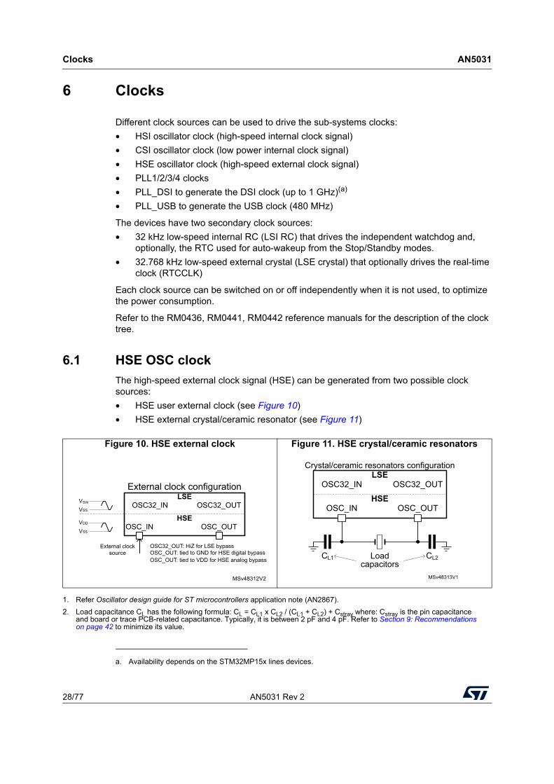
6.1 HSE OSC clock
The high-speed external clock signal (HSE) can be generated from two possible clock sources:
• HSE user external clock (see Figure 10)
• HSE external crystal/ceramic resonator (see Figure 11)
1. Refer Oscillator design guide for ST microcontrollers application note (AN2867).
2. Load capacitance CL has the following formula: CL = CL1 x CL2 / (CL1 + CL2) + Cstray where: Cstray is the pin capacitance and board or trace PCB-related capacitance. Typically, it is between 2 pF and 4 pF. Refer to Section 9: Recommendations on page 42 to minimize its value.
a. Availability depends on the STM32MP15x lines devices.
Figure 10. HSE external clock Figure 11. HSE crystal/ceramic resonators
OSC_IN OSC_OUT
External clock source
OSC32_IN OSC32_OUT
OSC32_OUT: HiZ for LSE bypass
External clock configuration
VDD
VSS
VSW
VSS
LSE
HSE
MSv48312V2
OSC_OUT: tied to GND for HSE digital bypassOSC_OUT: tied to VDD for HSE analog bypass
OSC_IN OSC_OUT
Loadcapacitors
OSC32_IN OSC32_OUT
CL1 CL2
Crystal/ceramic resonators configurationLSE
HSE
MSv48313V1
AN5031 Rev 2 29/77
AN5031 Clocks
76
6.1.1 External source (HSE bypass)
In this mode, an external clock source must be provided. It can have a frequency from 8 to 50 MHz (refer to STM32MP15x datasheets for actual max value).
The external digital (VIL/VIH) or analog (amplitude of 200 mV pk-pk minimum) clock signal with a duty cycle of about 50%, has to drive the OSC_IN pin.
Note: In order to allow USB boot, the BootROM automatically selects the HSE mode by checking the OSC_OUT connection during startup phase (that is on NRST rising edge):
– OSC_OUT is tied to GND (max 1 Kohm): HSE digital bypass
– OSC_OUT is tied to VDD (max 1 Kohm): HSE analog bypass
– OSC_OUT high-impedance or connected to a crystal/ceramic resonator: HSE crystal/ceramic resonator mode.
When Bypass is used, the external clock generator could be enabled by PWR_ON to save power (that is disabled in Standby). In that case, the OSC_IN clock input should be stable within 10 ms after the PWR_ON rising edge occurs.
6.1.2 External crystal/ceramic resonator (HSE crystal)
The external oscillator frequency ranges from 8 to 48 MHz.
The external oscillator has the advantage of producing a very accurate rate on the main clock. The associated hardware configuration is shown in Figure 11. Using a 24 MHz crystal frequency is a good choice to get accurate USB high-speed clocks.
The crystal/ceramic resonator and the load capacitors have to be connected as close as possible to the oscillator pins in order to minimize output distortion and startup stabilization time. The load capacitance values must be adjusted according to the selected crystal/ceramic resonator.
For CL1 and CL2 it is recommended to use NP0/C0G capacitors in the 5 pF-to-25 pF range (typ.), selected to meet the load requirements of the crystal/ceramic resonator. CL1 and CL2, have usually the same value. The crystal manufacturer typically specifies a load capacitance that is the series combination of CL1 and CL2. The PCB and pin capacitances must be included when sizing CL1 and CL2 (10 pF can be used as a rough estimate of the combined pin and board capacitance).
Refer to oscillator design guide for ST microcontrollers application note (AN2867) and electrical characteristics sections in the product datasheet for more details.

Clocks AN5031
30/77 AN5031 Rev 2
6.2 LSE OSC clock
The low-speed external clock signal (LSE) can be generated from two possible clock sources:
• LSE user external clock (see Figure 12)
• LSE external crystal/ceramic resonator (see Figure 13)
1. “LSE crystal/ceramic resonators” figure: It is strongly recommended to use a resonator with a load capacitance CL ≤ 12.5 pF.
2. “LSE external clock” and “LSE crystal/ceramic resonators” figures: OSC32_IN and OSC32_OUT pins can be used also as GPIO, but it is recommended not to use them as both RTC and GPIO pins in the same application.
6.2.1 External source (LSE bypass)
In this mode, an external clock source must be provided. It can have a frequency of up to 1 MHz. The external digital (VIL/VIH) or analog (amplitude of 200 mV pk-pk minimum) clock signal with a duty cycle of about 50% has to drive the OSC32_IN pin while the OSC32_OUT pin must be left high impedance (see Figure 12). The configuration of the bypass mode as well as the selection between the digital and analog is done within RCC registers
6.2.2 External crystal/ceramic resonator (LSE crystal)
The LSE crystal is a 32.768 kHz low-speed external crystal or ceramic resonator. It has the advantage of providing a low-power, but highly accurate clock source to the real-time clock peripheral (RTC) for clock/calendar or other timing functions.
The resonator and the load capacitors have to be connected as close as possible to the oscillator pins in order to minimize output distortion and startup stabilization time. The load capacitance values CL1 and CL2 must be adjusted according to the selected oscillator.
Refer to Oscillator design guide for ST microcontrollers dedicated application note (AN2867) and electrical characteristics sections in the product datasheet for more details.
Figure 12. LSE external clock Figure 13. LSE crystal/ceramic resonators
OSC_IN OSC_OUT
External clock source
OSC32_IN OSC32_OUT
OSC32_OUT: HiZ for LSE bypass
External clock configuration
VDD
VSS
VSW
VSS
LSE
HSE
MSv48312V2
OSC_OUT: tied to GND for HSE digital bypassOSC_OUT: tied to VDD for HSE analog bypass
OSC_IN OSC_OUT
Loadcapacitors
OSC32_IN OSC32_OUT
CL1 CL2
Crystal/ceramic resonators configurationLSE
HSE
MSv48313V1
AN5031 Rev 2 31/77
AN5031 Clocks
76
6.3 Clock security system (CSS)
Details can be found in the product reference manual (See Table 1: Reference documents).
6.3.1 CSS on HSE
The clock security system can be activated by software. In this case, the clock detector is enabled after the HSE oscillator startup delay, and disabled when this oscillator is stopped.
• If a failure is detected on the HSE oscillator clock, a system reset can be generated as well as signaled to the TAMP block for security protection.
6.3.2 CSS on LSE
The clock security system can be activated by software. In this case, the clock detector is enabled after the LSE oscillator startup delay, and disabled when this oscillator is stopped.
• If a failure is detected on the LSE oscillator clock, the RTC/TAMP clock source is stopped as well as signaled to the TAMP block for security protection.
Boot configuration AN5031
32/77 AN5031 Rev 2
7 Boot configuration
7.1 Boot mode selection
In the STM32MP15x lines devices, different boot modes can be selected by means of the BOOT[2:0] pins. the reserved configuration is highlighted in gray in the table.
The values on the BOOT pins are sampled by BootROM after a reset. It is up to the user to set the BOOT[2:0] pins before reset exit to select the required boot mode.
The BOOT pins could also be resampled later by software (for example by reading SYSCFG.BOOTR_BOOT[2:0] field) or by the BootROM when exiting the Standby mode. Consequently, they must be kept in the required boot mode configuration all the time.
During Stop modes, when the BOOT[2:0] pins are connected to VDD, as the three embedded pull-down are enabled by default, some current is flowing thru the pull-down. In order to save some tens of μA of power, the software could disable the pull-down on pins which are connected to VDD by simply setting field SYSCFG_BOOTR.BOOT[2:0]_PD equal to value read in SYSCFG_BOOTR.BOOT[2:0] field. This must be done again after each Standby exit as the SYSCFG_BOOTR register is reset. Note that during Standby, the BOOT[2:0] pins are set in tri-state and no current is flowing in BOOT[2:0] pins even if connected to VDD.
Table 12. Boot modes
BOOT2 BOOT1 BOOT0 Initial boot mode Comments
0 0 0 UART and USB(1)Wait incoming connection on:
– USART2/3/6 and UART4/5/7/8 on default pins
– USB High-Speed device on OTG_HS_DP/DM pins(2)
0 0 1 Serial NOR-Flash(3) Serial NOR-Flash on QUADSPI(5)
0 1 0 eMMC™(3) eMMC™ on SDMMC2 (default)(5)(6)
0 1 1 NAND-Flash(3) SLC NAND-Flash on FMC
1 0 0 Reserved Used to get debug access without boot from Flash(4)
1 0 1 SD-Card(3) SD-Card on SDMMC1 (default)(5)(6)
1 1 0 UART and USB(1)(3)Wait incoming connection on:
– USART2/3/6 and UART4/5/7/8 on default pins
– USB High-speed device on OTG_HS_DP/DM pins(2)
1 1 1 Serial NAND-Flash(3) Serial NAND-Flash on QUADSPI (5)
1. Could be disabled by OTP settings.
2. USB requires 24 MHz HSE clock/crystal if OTP is not programmed for different frequency (See Section 7.3: Embedded boot loader mode).
3. Boot source could be changed by OTP settings (such as Initial boot on SD-Card, then eMMC with OTP settings).
4. Cortex-A7 Core0 in infinite loop toggling PA13, Cortex-M4 in infinite loop on RETRAM.
5. Default pins can be altered by OTP.
6. Alternatively, another SDMMC interface than this default can be selected by OTP.

AN5031 Rev 2 33/77
AN5031 Boot configuration
76
7.2 Boot pin connection
Figure 14 shows an example of the external connection required to select the boot memory of the STM32MP15x lines devices.
Figure 14. Boot mode selection example
Despite all the recovery cases in software, there is a risk that with wrong or corrupted Flash content (such as: user mistake, bad Flash content programmed, power lost), the system might not start (also known as ‘bricked’).
Note that on empty Flash, the boot code automatically switches to UART/USB connection.
It might be required to have a way to force use of UART/USB connection in order to allow board Flash re-programming (for example: after sale services, firmware update).
There are also cases of where initial boot is done on a different Flash than regular boot (for example the initial boot from SD-Card, which copies binary data in another Flash like Serial NOR, Serial NAND, eMMC or SLC NAND). This is possible as the initial boot code could set relevant OTP bits to force future boot from the programmed Flash (see Figure 16). This allows a simplified and flexible mass production without intervention on BOOT pins.
The typical connections examples for final board are described in Figure 15.
The ‘switches’ could be done by various ways: pushbutton, solder bridges, connector contacts, test points, etc…, but assumed ‘open’ by default during normal product boot to avoid current flow in external resistors.
Note that OTP configuration could force or forbid any of the boot sources in order to satisfy product security requirements.
BOOT2
RP
D
SYSCFG_BOOTR.BOOT2
SYSCFG_BOOTR.BOOT2_PD
VDD
BOOT1
RP
D
SYSCFG_BOOTR.BOOT1
SYSCFG_BOOTR.BOOT1_PD
VDD
BOOT0
RP
D
SYSCFG_BOOTR.BOOT0
SYSCFG_BOOTR.BOOT0_PD
MSv48314V1
SW3
SW2
SW1
VDD
1K
BP3
BP2
1K
VDD
1K
BP1
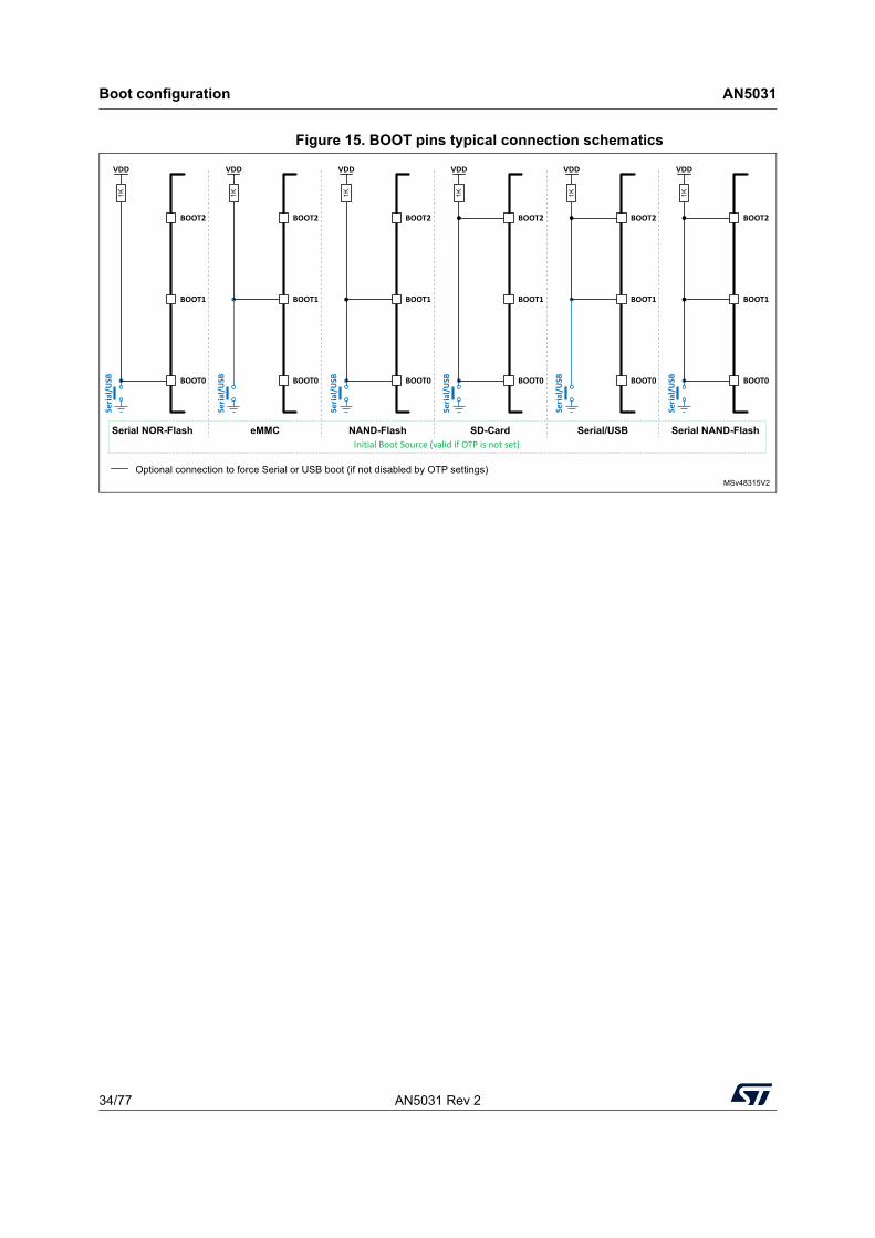
Boot configuration AN5031
34/77 AN5031 Rev 2
Figure 15. BOOT pins typical connection schematics
Optional connection to force Serial or USB boot (if not disabled by OTP settings)MSv48315V2
Serial NOR-Flash NAND-Flash
BOOT2
BOOT1
BOOT0
eMMC SD-CardInitial Boot Source (valid if OTP is not set)
VDD
Seria
l/USB
1K
BOOT2
BOOT1
BOOT0
VDD
Seria
l/USB
1K
BOOT2
BOOT1
BOOT0
VDD
Seria
l/USB
1K
BOOT2
BOOT1
BOOT0
VDD
Seria
l/USB
1K
Serial/USB
BOOT2
BOOT1
BOOT0
VDD
Seria
l/USB
1K
Serial NAND-Flash
BOOT2
BOOT1
BOOT0
VDD
Seria
l/USB
1K
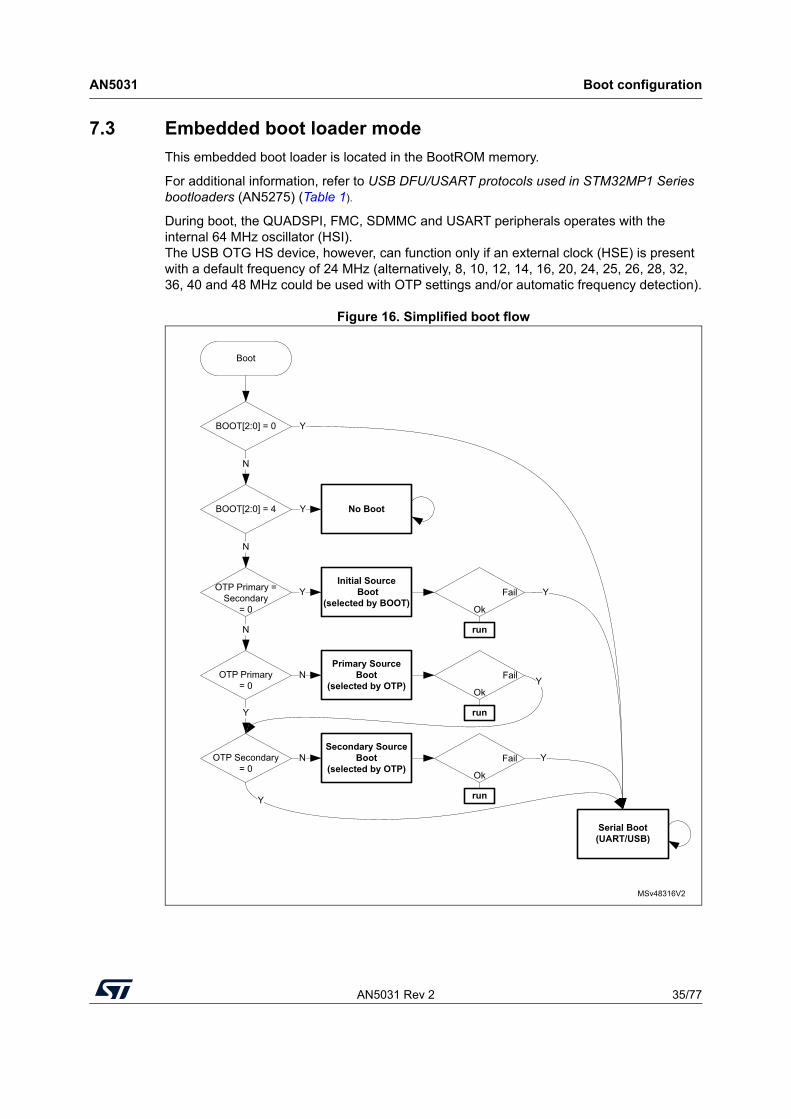
AN5031 Rev 2 35/77
AN5031 Boot configuration
76
7.3 Embedded boot loader mode
This embedded boot loader is located in the BootROM memory.
For additional information, refer to USB DFU/USART protocols used in STM32MP1 Series bootloaders (AN5275) (Table 1).
During boot, the QUADSPI, FMC, SDMMC and USART peripherals operates with the internal 64 MHz oscillator (HSI). The USB OTG HS device, however, can function only if an external clock (HSE) is present with a default frequency of 24 MHz (alternatively, 8, 10, 12, 14, 16, 20, 24, 25, 26, 28, 32, 36, 40 and 48 MHz could be used with OTP settings and/or automatic frequency detection).
Figure 16. Simplified boot flow
Boot
Serial Boot(UART/USB)
Primary Source Boot
(selected by OTP)
Secondary Source Boot
(selected by OTP)
BOOT[2:0] = 0
BOOT[2:0] = 4 Y
N
OTP Primary = 0
N
Initial Source Boot
(selected by BOOT)Ok
Y
Ok
OTP Secondary = 0
Y
N
NY
Y
run
run
run
Y
No Boot
Y
OTP Primary = Secondary
= 0
Y
N
MSv48316V2
Ok
Fail
Fail
Fail

Debug management AN5031
36/77 AN5031 Rev 2
8 Debug management
8.1 Introduction
The Host/target interface is the hardware equipment that connects the host to the application board. This interface is made of three components: a hardware debug tool, a JTAG or SWD connector and a cable connecting the host to the debug tool.
Figure 17 shows the connection of the host to the evaluation board.
Figure 17. Host-to-board connection
8.2 SWJ debug port (serial wire and JTAG)
The STM32MP15x lines core integrates the Serial Wire / JTAG debug port (SWJ-DP). It is an Arm® standard CoreSight™ debug port that combines a JTAG-DP (5-pin) interface and a SW-DP (2-pin) interface.
• The JTAG debug port (JTAG-DP) provides a 5-pin standard JTAG interface to the AHP-AP port
• The serial wire debug port (SW-DP) provides a 2-pin (clock + data) interface to the AHB-AP port
The two pins of the SW-DP are multiplexed with two of the five JTAG pins of the JTAG-DP.
8.3 Pinout and debug port pins
8.3.1 Internal pull-up and pull-down resistors on JTAG pins
To avoid any uncontrolled I/O levels, the STM32MP15x lines embed internal pull-up and pull-down resistors on JTAG pins:
• NJTRST: Internal pull-up
• JTDI: Internal pull-up
• JTDO-TRACESWO: Internal pull-up
• JTMS-SWDIO: Internal pull-up
• JTCK-SWCLK: Internal pull-down
Evaluation boardHost PC Power supply
SWD connectorDebug tool
ai14866c
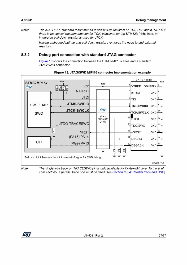
AN5031 Rev 2 37/77
AN5031 Debug management
76
Note: The JTAG IEEE standard recommends to add pull-up resistors on TDI, TMS and nTRST but there is no special recommendation for TCK. However, for the STM32MP15x lines, an integrated pull-down resistor is used for JTCK.
Having embedded pull-up and pull-down resistors removes the need to add external resistors.
8.3.2 Debug port connection with standard JTAG connector
Figure 18 shows the connection between the STM32MP15x lines and a standard JTAG/SWD connector.
Figure 18. JTAG/SWD MIPI10 connector implementation example
Note: The single wire trace on TRACESWO pin is only available for Cortex-M4 core. To trace all cores activity, a parallel trace port must be used (see Section 8.3.4: Parallel trace and HDP).
VDDSTM32MP15x1 VTREF3 nTRST5 TDI7 TMS/SWDIO9 TCK/SWCLK
11 RTCK13
15 nSRST17 DBGRQ19 DBGACK
2
4
6
8
10
12
14
16
18
20
TDO/SWO
2 × 10 Header
NJTRST
JTDI
JTMS-SWDIO
JTCK-SWCLK
NRST
JTDO-TRACESWO10
k
10k
10k
VDD
MSv48317V1
VDD
RP
U
RP
U
SWJ / DAP
SWO
RP
U
RP
U
RP
D
(2 x )ESDALC6
V1W5
GND
GND
GND
GND
GND
GND
GND
GND
GND
VSUPPLYVDD
CTI(PA15) PA14
(PG9) PA13
Bold and thick lines are the minimum set of signal for SWD debug

Debug management AN5031
38/77 AN5031 Rev 2
8.3.3 Debug port and UART connection with STDC14 connector
Figure 19 shows the connection between the STM32MP15x lines and a STDC14 connector including UART virtual com port connection.
Reference example for STDC14 header is FTSH-107-01-L-DV-K-A
Figure 19. JTAG/SWD/UART VCP STDC14 connector implementation example
Note: The single wire trace on TRACESWO pin is only available for Cortex-M4 Core. To trace all cores activity, a parallel trace port must be used (see Section 8.3.4: Parallel trace and HDP).
Note: STDC14 connector is respecting (from pin 3 to pin 12) the Arm10 pinout (Arm Cortex debug connector).
VDD
STM32MP15x
JTDI
JTMS-SWDIO
JTCK-SWCLK
NRST
JTDO-TRACESWO
MSv61715V1
RP
U
RP
U
SWJ / DAP
SWO
RP
U
RP
D
(2 x)ESDALC6
V1W5
VDD
UART4PB2
PG11
Bold and thick lines, the minimum set of signal for SWD debug
UART4_RX
UART4_TX
1
3
5
7
9
11
13
2
4
6
8
10
12
14
Res.
T_VCC
GND
GND
T_JRCLK/NC
GNDDetect
T_VCP_RX
2 × 7 pitch 1.27mm
T_JTMS/T_SWDIO
T_JCLK/T_SWCLK
T_JTDO/T_SWO
T_JTDI/NC
T_NRST
T_VCP_TX
Res.
100
VDD
AN5031 Rev 2 39/77
AN5031 Debug management
76
8.3.4 Parallel trace and HDP
Parallel trace
TRACED[15:0] and TRACECLK signals are available as alternate functions on IOs pins. The user could select number of trace data N = 1, 2, 4, 8 or 16 pins. Less trace data mean lower available trace bandwidth, so less information could be traced (such as the number of trace sources, code and/or data tracing) without trace overrun (there is a 8 Kbytes buffer in STM32MP15x lines). For each product, a trade-off between available features and trace bus could lead to have reduced feature while using trace during product development.
The trace is compliant to Arm® CoreSight™ trace and needs a dedicated tracing tool in order to be interpreted and correlated with debugging done through SWD or JTAG.
For more information on the Trace Port Interface CoreSight™ component, refer to product reference manual and the Arm® CoreSight™ SoC-400 technical reference manual.
Note that for efficient tracing bandwidth, TRACECLK should run as fast as possible while maintaining good signal integrity on all parallel trace signals. This is dependent on board and connector choices, GPIO strength settings (GPIO_OSPEEDR registers) and VDD voltage. When using VDD = 1.8 V, a setting in the OTP bit and the register SYSCFG_IOCTRLSETR (HSLVEN_TRACE bit) could be required to ensure the best speed on pads used on trace signals.
Warning: UHSLVEN and HSLVEN must not be set when VDD is above 2.7 V otherwise permanent IC damage could occur.
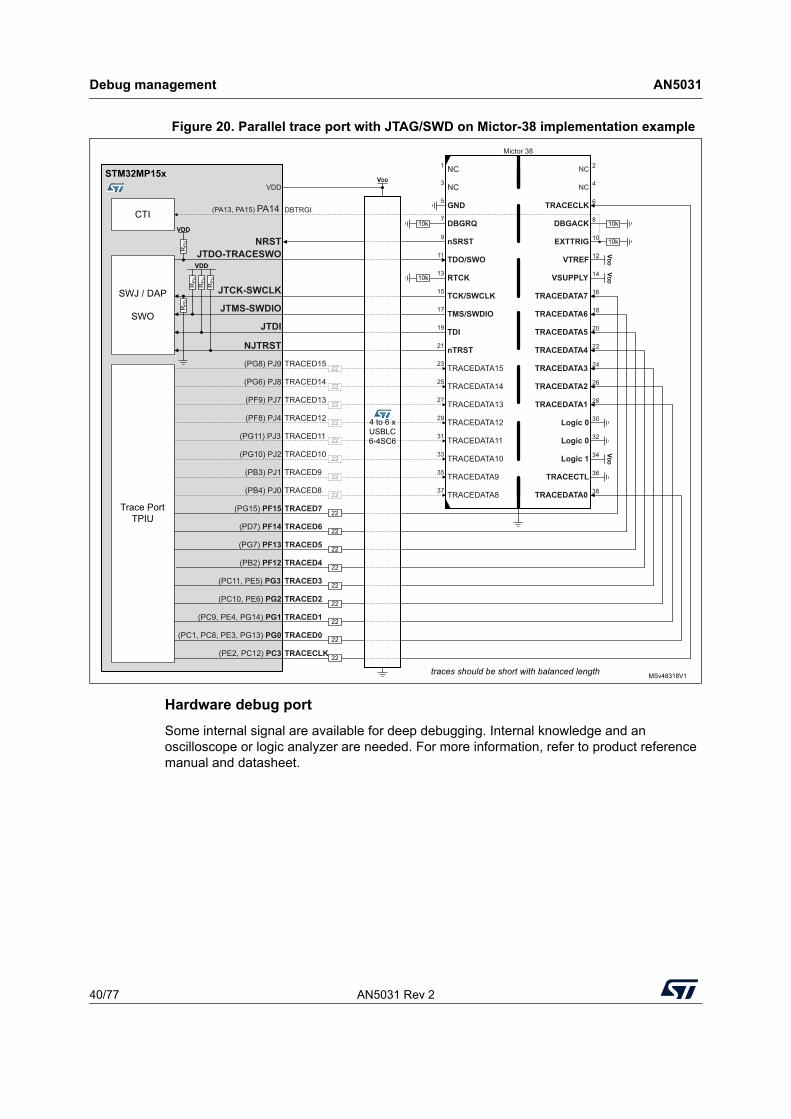
Debug management AN5031
40/77 AN5031 Rev 2
Figure 20. Parallel trace port with JTAG/SWD on Mictor-38 implementation example
Hardware debug port
Some internal signal are available for deep debugging. Internal knowledge and an oscilloscope or logic analyzer are needed. For more information, refer to product reference manual and datasheet.
VDDSTM32MP15x
1
GND
3
DBGRQ
5
nSRST
7
TDO/SWO
9
RTCK
11
TCK/SWCLK
13
15
TDI
17
nTRST
19
TRACEDATA15
2
4
6
8
10
12
14
16
18
20
TMS/SWDIO
NJTRST
JTDI
JTMS-SWDIO
JTCK-SWCLK
NRSTJTDO-TRACESWO
10k
10k
MSv48318V1
VDD
RP
U
RP
U
SWJ / DAP
SWO
RP
U
RP
U
RP
D
DBGACK
EXTTRIG
VTREF
VSUPPLY
TRACEDATA7
TRACEDATA6
TRACEDATA5
TRACEDATA4
TRACECLK
VDD
CTI (PA13, PA15) PA14
Trace PortTPIU
NC
NC NC
NC
21
23
25
27
29
31
33
35
37
22
24
26
28
30
32
34
36
38
TRACEDATA14
TRACEDATA13
TRACEDATA12
TRACEDATA11
TRACEDATA10
TRACEDATA9
TRACEDATA8
TRACEDATA3
TRACEDATA2
TRACEDATA1
Logic 0
Logic 0
Logic 1
TRACECTL
TRACEDATA0
VDD
10k
VD
DV
DD
4 to 6 x USBLC6-4SC6
TRACED15
TRACED14
TRACED13
TRACED12
TRACED11
TRACED10
TRACED9
TRACED8
TRACED7
TRACED6
TRACED5
TRACED4
TRACED3
TRACED2
TRACED1
TRACED0
TRACECLK
10k
VD
D
22
22
22
22
22
22
22
22
22
22
22
22
22
22
22
22
22
Mictor 38
(PE2, PC12) PC3
(PC1, PC8, PE3, PG13) PG0
(PC9, PE4, PG14) PG1
(PC10, PE6) PG2
(PC11, PE5) PG3
(PB2) PF12
(PG7) PF13
(PD7) PF14
(PG15) PF15
(PB4) PJ0
(PB3) PJ1
(PG10) PJ2
(PG11) PJ3
(PF8) PJ4
(PF9) PJ7
(PG6) PJ8
(PG8) PJ9
DBTRGI
traces should be short with balanced length
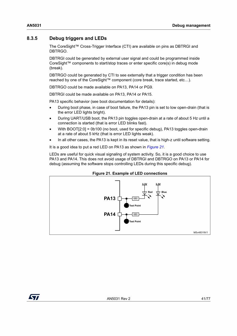
AN5031 Rev 2 41/77
AN5031 Debug management
76
8.3.5 Debug triggers and LEDs
The CoreSight™ Cross-Trigger Interface (CTI) are available on pins as DBTRGI and DBTRGO.
DBTRGI could be generated by external user signal and could be programmed inside CoreSight™ components to start/stop traces or enter specific core(s) in debug mode (break).
DBTRGO could be generated by CTI to see externally that a trigger condition has been reached by one of the CoreSight™ component (core break, trace started, etc…).
DBTRGO could be made available on PA13, PA14 or PG9.
DBTRGI could be made available on PA13, PA14 or PA15.
PA13 specific behavior (see boot documentation for details):
• During boot phase, in case of boot failure, the PA13 pin is set to low open-drain (that is the error LED lights bright).
• During UART/USB boot, the PA13 pin toggles open-drain at a rate of about 5 Hz until a connection is started (that is error LED blinks fast).
• With BOOT[2:0] = 0b100 (no boot, used for specific debug), PA13 toggles open-drain at a rate of about 5 kHz (that is error LED lights weak).
• In all other cases, the PA13 is kept in its reset value, that is high-z until software setting.
It is a good idea to put a red LED on PA13 as shown in Figure 21.
LEDs are useful for quick visual signaling of system activity. So, it is a good choice to use PA13 and PA14. This does not avoid usage of DBTRGI and DBTRGO on PA13 or PA14 for debug (assuming the software stops controlling LEDs during this specific debug).
Figure 21. Example of LED connections
680
3.3V
Red
3.3V
Blue
680
PA13
PA14
Test Point
Test Point
MSv48319V1

Recommendations AN5031
42/77 AN5031 Rev 2
9 Recommendations
9.1 Printed circuit board
For technical reasons, it is mandatory to use a multilayer printed circuit board (PCB) with a separate layer dedicated to ground (VSS) and another layer dedicated for power supplies like the VDD and VDDCORE. This provides good decoupling and a good shielding effect.
9.2 Component position
A preliminary layout of the PCB must separate the different circuits according to their EMI contribution in order to reduce cross-coupling on the PCB, that is noisy, high-current circuits, low-voltage circuits, and digital components.
9.3 Ground and power supply (VSSx, VDDx)
Due to large power and high frequencies involved in STM32MP15x lines, it is mandatory to use at least 4 layers PCB with dedicated power planes for VSSx and VDDx.
9.4 IO speed settings
It is important to set the right output drive on IOs in order to have sufficient rise and fall time, but also avoid additional ringing and noise.
When there is no specific requirements for IO speed, it is mandatory to set OSPEEDR to 0.
As a first approximation, the following drawing and tables could be used to quickly choose the right setting to apply according to signal frequency and capacitive load. This setting might need to be tailored in case of signal integrity issue.
In most cases, IO compensation needs to be enabled in SYSCFG. Refer to product datasheet for more details.
Note: In case of asynchronous or single edge clocked data lanes (such as SDR), the maximum data frequency toggle is effectively half the data rate. For example an SPI running at 10 Mbits/s has a maximum frequency of 5 MHz on data signal (for example output serial data 01010101...), but 10 MHz on the clock signal. On dual edge clocked data lanes (such as DDR), the clock and data have same maximum toggling frequency.
Note: The HSLVEN_xxx bits are not taken into account if the OTP bit PRODUCT_BELOW_2V5 =0 (default state).
Note: Setting HSLVEN_xxx=1 and product_below_2V5=1 while VDD > 2.7V can damage the IC.
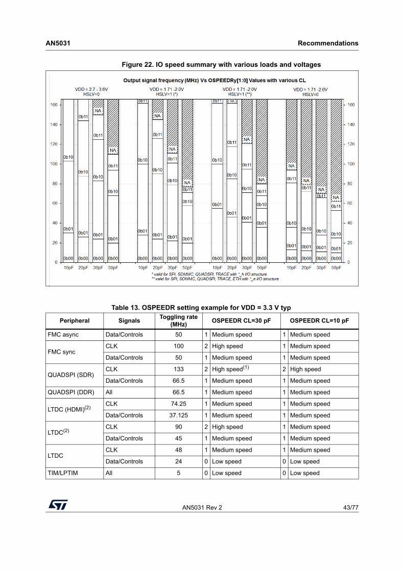
AN5031 Rev 2 43/77
AN5031 Recommendations
76
Figure 22. IO speed summary with various loads and voltages
Table 13. OSPEEDR setting example for VDD = 3.3 V typ
Peripheral SignalsToggling rate
(MHz)OSPEEDR CL=30 pF OSPEEDR CL=10 pF
FMC async Data/Controls 50 1 Medium speed 1 Medium speed
FMC syncCLK 100 2 High speed 1 Medium speed
Data/Controls 50 1 Medium speed 1 Medium speed
QUADSPI (SDR)CLK 133 2 High speed(1) 2 High speed
Data/Controls 66.5 1 Medium speed 1 Medium speed
QUADSPI (DDR) All 66.5 1 Medium speed 1 Medium speed
LTDC (HDMI)(2)CLK 74.25 1 Medium speed 1 Medium speed
Data/Controls 37.125 1 Medium speed 1 Medium speed
LTDC(2)CLK 90 2 High speed 1 Medium speed
Data/Controls 45 1 Medium speed 1 Medium speed
LTDCCLK 48 1 Medium speed 1 Medium speed
Data/Controls 24 0 Low speed 0 Low speed
TIM/LPTIM All 5 0 Low speed 0 Low speed
Recommendations AN5031
44/77 AN5031 Rev 2
I2C All 1 0 Low speed 0 Low speed
USART All 5 0 Low speed 0 Low speed
SPICLK 50 1 Medium speed 1 Medium speed
Data/Controls 25 1 Medium speed 0 Low speed
SAI
MCLK 15 0 Low speed 0 Low speed
CLK 1 0 Low speed 0 Low speed
Data/Controls 0.5 0 Low speed 0 Low speed
MDIOS All 5 0 Low speed 0 Low speed
SDMMC (SDR)CLK 133 2 High speed(1) 2 High speed
Data/Controls 66.5 1 Medium speed 1 Medium speed
SDMMC (DDR) All 52 1 Medium speed 1 Medium speed
FDCAN All 5 0 Low speed 0 Low speed
ETH (MII)CLK 50 1 Medium speed 1 Medium speed
Data/Controls 25 1 Medium speed 0 Low speed
ETH (RMII) All 50 1 Medium speed 1 Medium speed
ETH (GMII)CLK 125 2 High speed 2 High speed
Data/Controls 62.5 1 Medium speed 1 Medium speed
ETH (RGMII) All 125 2 High speed 2 High speed
ETH (MDIO) MDIO 2.5 0 Low speed 0 Low speed
TRACE All133 3 Very high speed 2 High speed
100 2 High speed 1 Medium speed
1. Value for CL=20 pF.
2. Requires External Oscillator for HSE.
Table 13. OSPEEDR setting example for VDD = 3.3 V typ (continued)
Peripheral SignalsToggling rate
(MHz)OSPEEDR CL=30 pF OSPEEDR CL=10 pF
Table 14. OSPEEDR setting example for VDD = 1.8 V typ.(1)
Peripheral SignalsToggling rate
(MHz)OSPEEDR CL=30 pF OSPEEDR CL=10 pF
FMC async Data/Controls 50 2 High speed 2 High speed
FMC syncCLK 69 3 Very high speed 3 Very high speed
Data/Controls 34.5 2 High speed 1 Medium speed
QUADSPI (SDR)(2)CLK 133 3 Very high speed(3) 2 High speed
Data/Controls 66.5 1 Medium speed 1 Medium speed
QUADSPI (DDR)(2) All 66.5 1 Medium speed 1 Medium speed
LTDC (HDMI)CLK 74.25 3 Very high speed(3) 3 Very high speed
Data/Controls 37.125 2 High speed 2 High speed
AN5031 Rev 2 45/77
AN5031 Recommendations
76
LTDCCLK 69 3 Very high speed 3 Very high speed
Data/Controls 34.5 2 High speed 1 Medium speed
TIM/LPTIM All 5 0 Low speed 0 Low speed
I2C All 1 0 Low speed 0 Low speed
USART All 5 0 Low speed 0 Low speed
SPI(4)CLK 50 1 Medium speed 1 Medium speed
Data/Controls 25 1 Medium speed 0 Low speed
SAI
MCLK 15 1 Medium speed 1 Medium speed
CLK 1 0 Low speed 0 Low speed
Data/Controls 0.5 0 Low speed 0 Low speed
MDIOS All 5 0 Low speed 0 Low speed
SDMMC (SDR)(5)CLK 133 3 Very high speed(3) 2 High speed
Data/Controls 66.5 1 Medium speed 1 Medium speed
SDMMC (DDR)(5) All 52 1 Medium speed 1 Medium speed
FDCAN All 5 0 Low speed 0 Low speed
ETH (MII)(6)CLK 50 1 Medium speed 0 Low speed
Data/Controls 25 0 Low speed 0 Low speed
ETH (RMII)(6) All 50 1 Medium speed 0 Low speed
ETH (GMII)(6)CLK 125 3 Very high speed(3) 2 High speed
Data/Controls 62.5 1 Medium speed 1 Medium speed
ETH (RGMII)(6) All 125 3 Very high speed(3) 2 High speed
ETH (MDIO) MDIO 2.5 0 Low speed 0 Low speed
TRACE(7) All133 3 Very high speed(3) 2 High speed
100 2 High speed 1 Medium speed
1. HSLVEN_xxx=1 are only taken into account if OTP bit PRODUCT_BELOW_2V5 is set.
2. HSLVEN_QUADSPI=1.
3. Value for CL=20pF.
4. HSLVEN_SPI=1.
5. HSLVEN_SDMMC=1.
6. HSLVEN_ETH=1.
7. HSLVEN_TRACE=1.
Table 14. OSPEEDR setting example for VDD = 1.8 V typ.(1) (continued)
Peripheral SignalsToggling rate
(MHz)OSPEEDR CL=30 pF OSPEEDR CL=10 pF
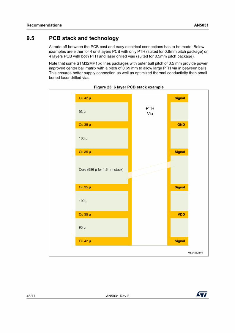
Recommendations AN5031
46/77 AN5031 Rev 2
9.5 PCB stack and technology
A trade off between the PCB cost and easy electrical connections has to be made. Below examples are either for 4 or 6 layers PCB with only PTH (suited for 0.8mm pitch package) or 4 layers PCB with both PTH and laser drilled vias (suited for 0.5mm pitch package).
Note that some STM32MP15x lines packages with outer ball pitch of 0.5 mm provide power improved center ball matrix with a pitch of 0.65 mm to allow large PTH via in between balls. This ensures better supply connection as well as optimized thermal conductivity than small buried laser drilled vias.
Figure 23. 6 layer PCB stack example
Cu 42 μ
Cu 35 μ
Cu 35 μ
Cu 35 μ
Cu 35 μ
Cu 42 μ
Signal
93 μ
GND
100 μ
Signal
Core (986 μ for 1.6mm stack)
Signal
100 μ
VDD
93 μ
Signal
PTHVia
MSv48321V1
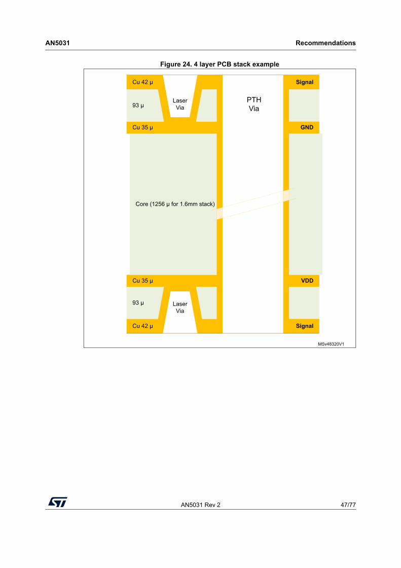
AN5031 Rev 2 47/77
AN5031 Recommendations
76
Figure 24. 4 layer PCB stack example
Cu 42 μ
Cu 35 μ
Cu 35 μ
Cu 42 μ
Signal
93 μ
GND
VDD
93 μ
Signal
MSv48320V1
Core (1256 μ for 1.6mm stack)
PTHVia
LaserVia
LaserVia

Recommendations AN5031
48/77 AN5031 Rev 2
Figure 25. PCB rule example for 0.8 mm pitch package
3.5 mils 90 μ Track
3.5 mils90 μ Track
MSv48322V1
Clearance
Ø320 μ
Pitch 0.8 mm
4 mils100 μLanding pad
For 400 μ Ball
4 mils100 μ
Ø400 μ
PTH Via200 μ

AN5031 Rev 2 49/77
AN5031 Recommendations
76
Figure 26. PCB rule example for 0.5 mm pitch package
Figure 27. PCB rule example for inner balls with 0.65mm power improved pitch
Clearance
MSv48323V1
3.5 mils90 μ Trac
k
Ø240 μ
Pitch 0.5 mm
Landing padFor 300 μ Ball
Ø400 μ
Ø250 or 275 μ PTH Via200 μ
Laser Via
100 μ
200 μ PTH Via possible only outside
0.5mm matrix
3 mils80 μ
MSv48324V1
Ø240 μ
Landing padFor 300 μ
Ball
PTH Via200 μ
Ø400 μ
PTH Via
3 mils 80 μ
Innex matrix power improved pitch 0.650 mm
Clearance
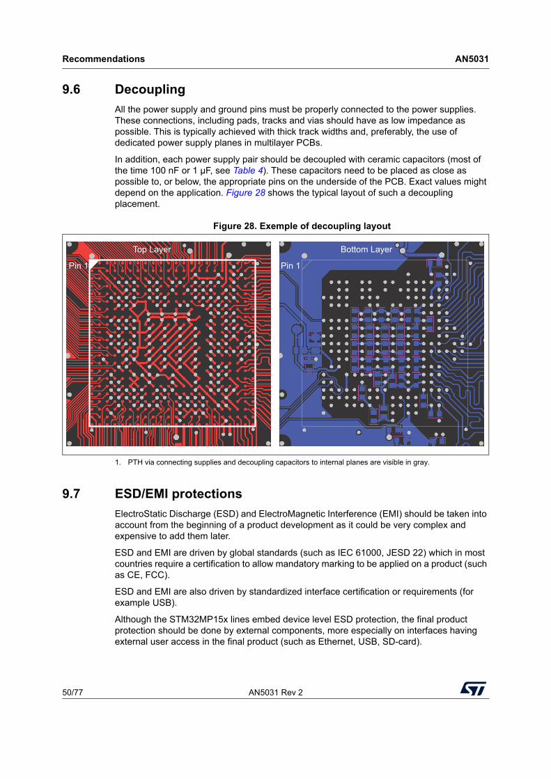
Recommendations AN5031
50/77 AN5031 Rev 2
9.6 Decoupling
All the power supply and ground pins must be properly connected to the power supplies. These connections, including pads, tracks and vias should have as low impedance as possible. This is typically achieved with thick track widths and, preferably, the use of dedicated power supply planes in multilayer PCBs.
In addition, each power supply pair should be decoupled with ceramic capacitors (most of the time 100 nF or 1 µF, see Table 4). These capacitors need to be placed as close as possible to, or below, the appropriate pins on the underside of the PCB. Exact values might depend on the application. Figure 28 shows the typical layout of such a decoupling placement.
Figure 28. Exemple of decoupling layout
1. PTH via connecting supplies and decoupling capacitors to internal planes are visible in gray.
9.7 ESD/EMI protections
ElectroStatic Discharge (ESD) and ElectroMagnetic Interference (EMI) should be taken into account from the beginning of a product development as it could be very complex and expensive to add them later.
ESD and EMI are driven by global standards (such as IEC 61000, JESD 22) which in most countries require a certification to allow mandatory marking to be applied on a product (such as CE, FCC).
ESD and EMI are also driven by standardized interface certification or requirements (for example USB).
Although the STM32MP15x lines embed device level ESD protection, the final product protection should be done by external components, more especially on interfaces having external user access in the final product (such as Ethernet, USB, SD-card).
Top Layer Bottom Layer
Pin 1 Pin 1
AN5031 Rev 2 51/77
AN5031 Recommendations
76
Some components provide ESD protection as well as EMI common mode filtering (for example ECMF02-2AMX6 used on USB).
Some examples of ESD/EMI protections are provided in Section 10: Reference design examples.
For more details, refer to EMC design guide for ST microcontrollers application note (AN1709).
9.8 Sensitive signals
When designing an application, the ElectroMagnetic Compatibility (EMC) performance can be improved by closely studying:
• Signals for which a temporary disturbance affects the running process permanently (the case of interrupts and handshaking strobe signals, and not the case for LED commands). For these signals, a surrounding ground trace, shorter lengths and the absence of noisy and sensitive traces nearby (crosstalk effect) improve the EMC performance. For digital signals, the best possible electrical margin must be reached for the two logical states and slow Schmitt triggers are recommended to eliminate parasitic states.
• Noisy signals (clock, etc.)
• Sensitive signals (high impedance, etc.)
For more details, refer to EMC design guide for ST microcontrollers application (AN1709).
9.9 Unused I/Os and features
The STM32MP15x lines are designed for a wide range of applications and often a particular application does not use 100% of the resources.
To increase the EMC performance, unused clocks, counters or I/Os, should not be left free, for example I/Os should be set to “0” or “1” (pull-up or pull-down to the unused I/O pins) and unused features should be “frozen” or disabled.
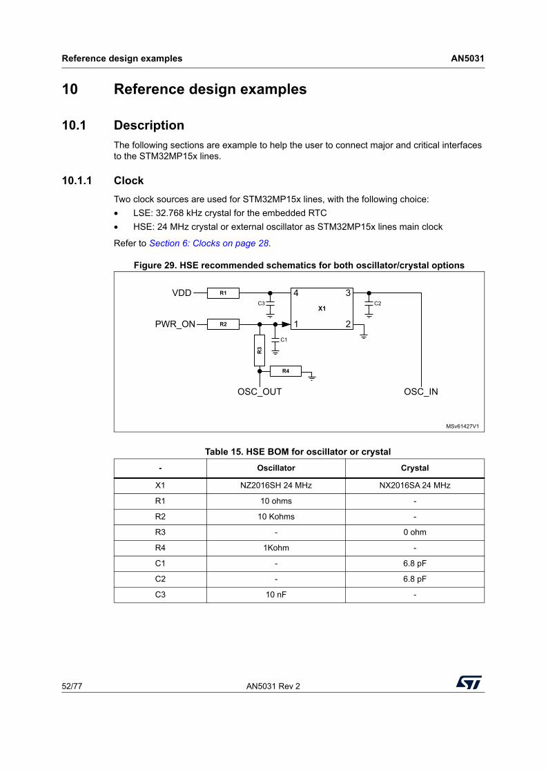
Reference design examples AN5031
52/77 AN5031 Rev 2
10 Reference design examples
10.1 Description
The following sections are example to help the user to connect major and critical interfaces to the STM32MP15x lines.
10.1.1 Clock
Two clock sources are used for STM32MP15x lines, with the following choice:
• LSE: 32.768 kHz crystal for the embedded RTC
• HSE: 24 MHz crystal or external oscillator as STM32MP15x lines main clock
Refer to Section 6: Clocks on page 28.
Figure 29. HSE recommended schematics for both oscillator/crystal options
Table 15. HSE BOM for oscillator or crystal
- Oscillator Crystal
X1 NZ2016SH 24 MHz NX2016SA 24 MHz
R1 10 ohms -
R2 10 Kohms -
R3 - 0 ohm
R4 1Kohm -
C1 - 6.8 pF
C2 - 6.8 pF
C3 10 nF -
R1
C3
VDDC2
OSC_INOSC_OUT
R3
R2PWR_ONC1
R4
X1
4 3
21
MSv61427V1

AN5031 Rev 2 53/77
AN5031 Reference design examples
76
10.1.2 Reset
The NRST reset signal in Figure 4 is active low. The reset sources include:
• Reset button
• Debugging tools via the JTAG connector
Refer to Section 4.3: Reset and power supply supervisor on page 17.
10.1.3 Boot mode
The boot option is configured by setting permanent wires or switches SW3 (BOOT2), SW2 (BOOT1) and SW1 (BOOT0) and internal OTP. Refer to Section 7: Boot configuration on page 32.
In case of the UART boot using one of the possible U(S)ARTx_RX pins, (refer to STM32MP1 Series wiki), to avoid a floating signal sent to the host, until the initialization character is received and decoded by the BootROM, it is required to have a 10 kOhm VDD pull-up on the respective U(S)ARTx_TX pin.
10.1.4 SWD / JTAG interface
The reference design shows the connections between the STM32MP15x lines and some standard connector. Refer to Section 8: Debug management on page 36.
Note: If available, it is recommended to connect the debugger probe system reset pin to NRST in order to be able to reset the application from the debugger.
Table 16. UART possible boot pins
Peripheral Signal Pin
USART2RX PA3
TX PA2
USART3RX PB12
TX PB10
UART4(1)
1. Recommended default UART for Linux console (that is as VCP on STLINK STDC14 connector).
RX PB2
TX PG11
UART5RX PB5
TX PB13
USART6RX PC7
TX PC6
UART7RX PF6
TX PF7
UART8RX PE0
TX PE1

Reference design examples AN5031
54/77 AN5031 Rev 2
10.1.5 Power supply
Refer to Section 4: Power supplies on page 11.
Discrete supplies example with 3.3 V I/Os with DDR3L
This reference design example targets a simple 3.3 V IOs platform with low cost DDR3L without emphasis on power reduction. The Sleep/Stop/Standby modes are supported. LP-Stop and low power Standby with DDR3L retention could be supported but might have little interest due to the use of DDR3L which has not a low power target for self-refresh.
Refer also to STM32MP151, STM32MP153 and STM32MP157 discrete power supply hardware integration (AN5256).
Figure 30. Discrete supplies example 3.3 V I/Os with DDR3L
1. Additional SMPS components not shown.
2. Smaller NCP161AFCT330 could also be used.
3. The 10 nF capacitor on NRST_CORE pin could be removed if NRST_CORE is connected to NRST.
PMIC supplies example 3.3 V I/Os with DDR3L
This reference design example targets a complex 3.3 V IOs platform with low cost DDR3L and high integration PMIC. Usually, all platform components can be powered by the PMIC. Full power supply control is supported thanks to PMIC I2C and side band signals. The Sleep/Stop/Standby modes are supported. See PMIC documentations for details of PMIC components.
2.2 μF
3K 1%
2 × 100 nF
100 nF
STM32MP15x
VDD_DSI
VDD_PLL
VDD
VDDQ_DDR
VDD1V2_DSI_REG
VDD1V2_DSI_PHY
VDD3V3_USBFS
VDD3V3_USBHS
PDR_ON_CORE
PDR_ON
DDR_VREF
VSSA
VREF-
VREF+
VSS_DSI
VSS_USBHS
VDDA1V8_DSI
VDDA1V8_REG
USB_RREF
VDDA1V1_REG
only if internal VREFBUF disabled
VDDA
2 × (100 nF + 1 μF)
DDR_ZQ 240 1%
VSSN × 1 μF
VSS
VSS_USBHS
DSI
USB
DDR
ADC/DAC
240 1%
3V VBATor
BYPASS_REG1V8
VDD_ANA
VSS_ANA
VSS_PLL
VREFCA
VREFDQVDDQ
VSSQ ZQ
1 μF
2.2 μF
2.2 μF
N × 1 μF
4 × 1 μF
100 nF
VIN VDDCORE (1.2V)
VDD (3.3V)
VDD_DDR (1.35V)
Discrete supplies example3.3V I/Os with DDR3L
2 × 1 μF
or
1 μF
VDD
SMPS (1)
1.2V 2A
4.7 μHVDD (3.3V)
VSS
10 nF
(4.0 - 5.5V)
(8 × 1 μF)
(4 × 100 nF)
Single or dual DDR3L
with VTT terminated control lines
VDD (3.3V)
VDD_DDR (1.35V)
1 μF
10 μF 1K 1
%
100 nF 1K 1
%
acceptable for single DDR3L
without VTT terminations
VDD_DDR (1.35V)VTT (0.675V)
100 nF
2 × 10 μF
(2 x)
(2 x)
(2 x)
VREF (0.675V)
(ZQ) 240 1%
EN
10 nF
If needed, additional LDO or SMPS
(SD, eMMC, ETH, Display, etc..)
RESET
470k
Additional VIN protections if needed (ESD, surges,
noise, etc..)
Note: Alternatively, to ease routing and avoid long VREF lines,
VREF could be generated locally by a 1KΩ/1KΩ 1% resistor divider on VDDQ close to
each VREF pins
VDDCORE
PWR_ON
NRST_CORE
VSS
NRST
DDR3L memory
VDDA_1V8 (1.8V)
LDOLD39130SJ33R (2)
3.3V 300mAEN
VDD_USB (3.3V)
Alternative to
Support DDR
retention during
Standby
RT9026
S3VIN
GND
VLODIN
VDDQSNS
PGND VTTREF
VTTVTTSNS
PWR_LP
SMPS(1)
1.35V 1A
EN
Shutdwon VTT
during LP_Stop
and Standby
N × 1 μF
MSv48302V4
Schematic / components for dual DDR3L
3.3V LDO or power switch>100mA <200mΩ(e.g. TPS22902,
FPF2100) VDDA_1V8 (1.8V)
VDD_USB (3.3V)
ENVDD3V3_USBHS switch off
when VDDA1V8_REG is off
(mandatory IC requirement)
VDD (3.3V) for switchVIN for LDO
note: capacitor could be removed if NRST_CORE is connected to NRST
(3)

AN5031 Rev 2 55/77
AN5031 Reference design examples
76
Figure 31. PMIC example 3.3 V I/Os with DDR3L
2.2 μF
3K 1%
2 × 100 nF
100 nF
STM32MP15x
VDD_DSI
VDD_PLL
VDD
VDDQ_DDR
VDD1V2_DSI_REG
VDD1V2_DSI_PHY
VDD3V3_USBFS
VDD3V3_USBHS
PDR_ON_CORE
PDR_ON
DDR_VREF
VSSA
VREF-
VREF+
VSS_DSI
VSS_USBHS
VDDA1V8_DSI
VDDA1V8_REG
USB_RREF
VDDA1V1_REG
only if internal VREFBUF disabled
VDDA
2 × (100 nF + 1 μF)
DDR_ZQ 240 1%
VSSN × 1 μF
VSS
VSS_USBHS
DSI
USB
DDR
ADC/DAC
240 1%
3V VBATor
BYPASS_REG1V8
VDD_ANA
VSS_ANA
VSS_PLL
VREFCA
VREFDQVDDQ
VSSQ ZQ
1 μF
2.2 μF
2.2 μF
N × 1 μF
4 × 1 μF
100 nF
VDDCORE (1.2V)
VDD (3.3V)
VDD_USB (3.3V)1 μF
VDDCORE
VDDQ_DDR
PWR_ON
NRST_CORE
VDDA (2.9V)
VSS
VSS
10 nF
PC13 (RTC_OUT1)
PA0 (WKUP1)
PZ4 (I2C4_SCL)
PZ5 (I2C4_SDA)
free
free
VDD_USB (3.3V)
VDD_SD (2.9V)
VBUSSW (5.2V)
VBUS_OTG (5.2V)
VDDA (2.9V)
only useful if VBAT is supplied separately than VDD
And wake up during VBAT mode is required
VBST (5.2V)
VBST (5.2V)
VDD (3.3V)
VIN(4.0 - 5.5V)
NRST10 nFRESET
ON / INT
1k5
1k5
(on at powerup if SD-Card boot)
(on at powerup)
VDDVDD
STPMIC1A
VLX3
VLX1
VLX2
VLX_4
WAKEUP
PWRCTRLINTN
SCLSDA
VREF
LDO3OUT
VOUT2
VOUT1
VOUT3
LDO6OUT
LDO2OUT
LDO4OUT
LDO5OUT
BSTOUT
SWIN SWOUT
VBUSOTG
LDO1OUT
VOUT_4
VLXBST
BUCK1IN
BUCK2IN
BUCK3IN
BUCK4IN
LDO16IN
LDO25IN
LDO3IN
VIO
VIN
PONKEYN
RSTN
exposed thermal pad
PGND
PGND
PGND
PGND
PGND
GNDLDO
INTLDO
AGND
Additional VIN protections if
needed (ESD, surges, noise, etc..)
3.3V(on at powerup)
3.3V
(ranking after VDD)
N × 1 μF
VDD
VSS
DDR3L memory
VTT (0.675V)
VREF (0.675V)
VDD_DDR (1.35V)
(8 × 100 nF)
(4 × 100 nF)
(2 x)
(2 x)
(2 x)
(ZQ) 240 1%
PMIC supplies example3.3V I/Os with DDR3L
Only for 2 × 16-bit
Note: Alternatively, to ease routing and avoid long VREF lines,
VREF could be generated locally by a 1KΩ/1KΩ 1% resistor divider
on VDDQ close to each VREF pins
VDD_DDR (1.35V)
Schematic / components for dual DDR3L MSv48342V5
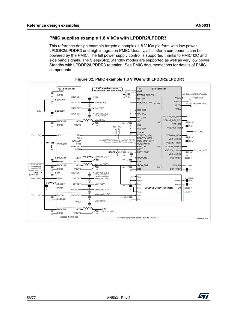
Reference design examples AN5031
56/77 AN5031 Rev 2
PMIC supplies example 1.8 V I/Os with LPDDR2/LPDDR3
This reference design example targets a complex 1.8 V IOs platform with low power LPDDR2/LPDDR3 and high integration PMIC. Usually, all platform components can be powered by the PMIC. The full power supply control is supported thanks to PMIC I2C and side band signals. The Sleep/Stop/Standby modes are supported as well as very low power Standby with LPDDR2/LPDDR3 retention. See PMIC documentations for details of PMIC components
Figure 32. PMIC example 1.8 V I/Os with LPDDR2/LPDDR3
2.2 μF
3K 1%
2 × 100 nF
100 nF
STM32MP15x
VDD_DSI
VDD_PLL
VDD
VDDQ_DDR
VDD1V2_DSI_REG
VDD1V2_DSI_PHY
VDD3V3_USBFS
VDD3V3_USBHS
PDR_ON_CORE
PDR_ON
DDR_VREF
VSSA
VREF-
VREF+
VSS_DSI
VSS_USBHS
VDDA1V8_DSI
VDDA1V8_REG
USB_RREF
VDDA1V1_REG
only if internal VREFBUF disabled
VDDA
2 × (100 nF + 1 μF)
DDR_ZQ 240 1%
VSSN × 1 μF
VSS
VSS_USBHS
DSI
USB
DDR
ADC/DAC
240 1%
3V VBATor
BYPASS_REG1V8
VDD_ANA
VSS_ANA
VSS_PLL
VREFCA
VREFDQVDDQ
VSSQ ZQ
1 μF
2.2 μF
2.2 μF
N × 1 μF
4 × 1 μF
100 nF
VDDCORE (1.2V)
VDD (1.8V)
VDD_USB (3.3V)1 μF
VDDCORE
VDDQ_DDR
PWR_ON
NRST_CORE
VDDA (2.9V)
VSS
VSS
10 nF
PC13 (RTC_OUT1)
PA0 (WKUP1)
PZ4 (I2C4_SCL)
PZ5 (I2C4_SDA)
VDD (1.8V)
free
free (2.9V)
VDD_USB (3.3V)
VDD_SD (2.9V)
VBUS_SW (5.2V)
VBUS_OTG (5.2V)
VDDA (2.9V)
only useful if VBAT is supplied separately than VDD
And wake up during VBAT mode is required
VBST (5.2V)
VBST (5.2V)
VDD (1.8V)
VIN(3.0 - 5.5V)
NRST10 nFRESET
ON / INT
1k5
1k5
(on at powerup)
(on at powerup)
VDDVDD
STPMIC1B
VLX3
VLX1
VLX2
VLX4
WAKEUP
PWRCTRLINTN
SCLSDA
VREF
LDO3OUT
VOUT2
VOUT1
VOUT3
LDO6OUT
LDO2OUT
LDO4OUT
LDO5OUT
BSTOUT
SWIN SWOUT
VBUSOTG
LDO1OUT
VOUT4
VLXBST
BUCK1IN
BUCK2IN
BUCK3IN
BUCK4IN
LDO16IN
LDO25IN
LDO3IN
VIO
VIN
PONKEYN
RSTN
exposed thermal pad
PGND
PGND
PGND
PGND
PGND
GNDLDO
INTLDO
AGND
Additional VIN protections if
needed (ESD, surges, noise, etc..)
3.3V(on at powerup)
3.3V
(ranking after VDD)
N × 1 μF
2 × 100 nF
VDDCA
VDD1
VSSCA
VDD2
VSS
LPDDR2/LPDDR3 memory
VDD1_DDR (1.8V)
VREF (0.6V)
VDD_DDR (1.2V)
(ZQ1) 240 1%
PMIC supplies example1.8V I/Os with LPDDR2/LPDDR3
Schematic / components on some dual-die LPDDR3 MSv48343V3
VDD (1.8V)
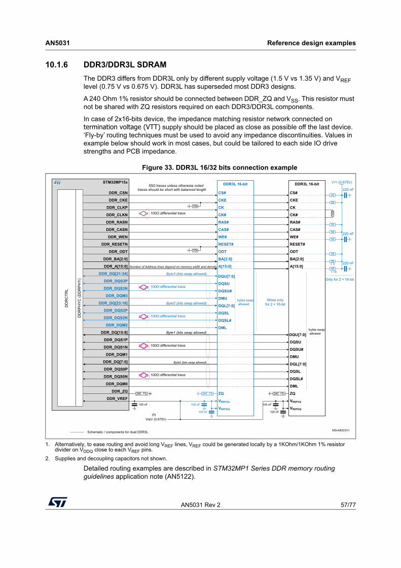
AN5031 Rev 2 57/77
AN5031 Reference design examples
76
10.1.6 DDR3/DDR3L SDRAM
The DDR3 differs from DDR3L only by different supply voltage (1.5 V vs 1.35 V) and VREF level (0.75 V vs 0.675 V). DDR3L has superseded most DDR3 designs.
A 240 Ohm 1% resistor should be connected between DDR_ZQ and VSS. This resistor must not be shared with ZQ resistors required on each DDR3/DDR3L components.
In case of 2x16-bits device, the impedance matching resistor network connected on termination voltage (VTT) supply should be placed as close as possible off the last device. ‘Fly-by’ routing techniques must be used to avoid any impedance discontinuities. Values in example below should work in most cases, but could be tailored to each side IO drive strengths and PCB impedance.
Figure 33. DDR3L 16/32 bits connection example
1. Alternatively, to ease routing and avoid long VREF lines, VREF could be generated locally by a 1KOhm/1KOhm 1% resistor divider on VDDQ close to each VREF pins.
2. Supplies and decoupling capacitors not shown.
Detailed routing examples are described in STM32MP1 Series DDR memory routing guidelines application note (AN5122).
DDR3L 16-bitSTM32MP15x
DDR_DQ[31:24]
DDR_DQS3P
DD
RC
TRL DDR_DQS3N
DDR_DQM3
DDR_DQS2N
DDR_DQ[23:16]
DDR_DQS2P
DDR_DQM2
DDR_DQS1P
DDR_DQS1N
DDR_DQM1
DDR_DQ[7:0]
DDR_DQS0P
DDR_DQS0N
DDR_DQM0
DDR_DQ[15:8]
DDR_BA[2:0]
DDR_ZQ
DDR_VREF
DDR_A[15:0]
DDR_WEN
DDR_RESETN
DDR_CASN
DQU[7:0]
DQSU
DQSU#
DMU
DQSL#
DQL[7:0]
DQSL
DML
BA[2:0]
ZQ
A[15:0]
WE#
RESET#
CAS#
VREFCA
VREFDQ
240 1% 240 1%
100 nF 100 nF
VREF (0.675V)
100 nF
DDR_CLKN
DDR_CKE
DDR_CLKP
DDR_CSN
CK#
CKE
CK
CS#
DDR_RASN RAS#
DDR_ODT ODT
DDR3L 16-bit
DQSU
DQSU#
DMU
DQL[7:0]
DQSL
DQSL#
DML
DQU[7:0]
BA[2:0]
ZQ
A[15:0]
WE#
RESET#
CAS#
VREFCA
VREFDQ
240 1%
100 nF
100 nF
CK#
CKE
CK
CS#
RAS#
ODT
56
56
56
56
56
56
56
56× 16
× 3 220 nF
220 nF
220 nF
VTT (0.675V)
Number of Address lines depend on memory width and density
Wires only for 2 × 16-bit
Only for 2 × 16-bit
MSv48303V1
10k
Byte3 (bits swap allowed)
Byte2 (bits swap allowed)
Byte1 (bits swap allowed)
Byte0 (bits swap allowed)
100Ω differential trace
55Ω traces unless otherwise noted
100Ω differential trace
100Ω differential trace
100Ω differential trace
100Ω differential trace
bytes swap allowed
100
10k
DD
RP
HY
C (D
DR
PH
Y)
traces should be short with balanced length
bytes swap allowed
Schematic / components for dual DDR3L
(1)
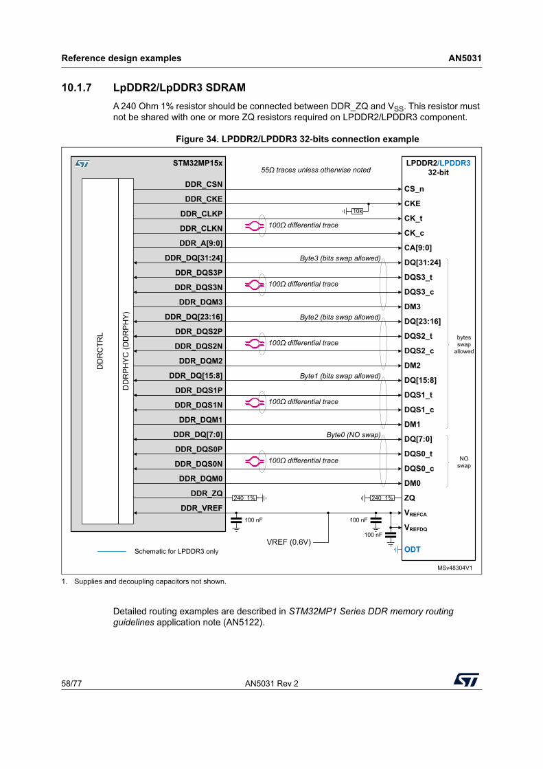
Reference design examples AN5031
58/77 AN5031 Rev 2
10.1.7 LpDDR2/LpDDR3 SDRAM
A 240 Ohm 1% resistor should be connected between DDR_ZQ and VSS. This resistor must not be shared with one or more ZQ resistors required on LPDDR2/LPDDR3 component.
Figure 34. LPDDR2/LPDDR3 32-bits connection example
1. Supplies and decoupling capacitors not shown.
Detailed routing examples are described in STM32MP1 Series DDR memory routing guidelines application note (AN5122).
STM32MP15x
DD
RC
TRL
DD
RP
HY
C (D
DR
PH
Y)
LPDDR2/LPDDR3 32-bit
DDR_DQ[31:24]
DDR_DQS3P
DDR_DQS3N
DDR_DQM3
DDR_DQS2N
DDR_DQ[23:16]
DDR_DQS2P
DDR_DQM2
DDR_DQS1P
DDR_DQS1N
DDR_DQM1
DDR_DQ[7:0]
DDR_DQS0P
DDR_DQS0N
DDR_DQM0
DDR_DQ[15:8]
DDR_CLKN
DDR_ZQ
DDR_VREF
DDR_A[9:0]
DDR_CKE
DDR_CLKP
DDR_CSN
DQ[31:24]
DQS3_t
DQS3_c
DM3
DQS2_c
DQ[23:16]
DQS2_t
DM2
DQS1_t
DQS1_c
DM1
DQ[7:0]
DQS0_t
DQS0_c
DM0
DQ[15:8]
CK_c
ZQ
CA[9:0]
CKE
CK_t
CS_n
VREFCA
VREFDQ
240 1% 240 1%
Byte3 (bits swap allowed)
Byte2 (bits swap allowed)
Byte1 (bits swap allowed)
Byte0 (NO swap)
100 nF 100 nF
VREF (0.6V)100 nF
ODT
MSv48304V1
10k
100Ω differential trace
100Ω differential trace
100Ω differential trace
100Ω differential trace
55Ω traces unless otherwise noted
100Ω differential trace
bytes swap
allowed
NO swap
Schematic for LPDDR3 only

AN5031 Rev 2 59/77
AN5031 Reference design examples
76
10.1.8 SD card
External level shifter
It allows the use of UHS-I faster modes (up to SDR50 and DDR50, that is 50 MBytes/s bus speed) which need to switch to 1.8 V card I/Os voltage (SD-card is started with 3 V card I/Os).
Note: As boot is always done in ‘Standard’ mode (3 V IOs), if the card is used by the application in USH-I, a power cycle on card supply is required after Reset or Standby.
This example is independent of MPU IO voltage VDD which could be between 1.71 V and 3.6 V. In case of VDD at 1.8 V typ, an external level shifter is mandatory as all SD-Card start transactions in 'Standard' mode using 3 V signaling voltage.
Note that a good signal integrity is dependent on board, GPIO strength settings (GPIO_OSPEEDR registers) and VDD voltage. When using VDD = 1.8 V, a setting in the OTP bit and the register SYSCFG_IOCTRLSETR (HSLVEN_SDMMC bit) could be required to ensure the best speed on pads used on SDMMC outputs.
Warning: UHSLVEN and HSLVEN must not be set when VDD is above 2.7 V otherwise permanent IC damage could occur.
If needed, the impedance matching resistor should be placed as close as possible of the output driver pin. Values in example below should work in most cases, but could be tailored to IO drive strengths and PCB impedance.

Reference design examples AN5031
60/77 AN5031 Rev 2
Figure 35. SD-Card with external level shifter connection example
1. SDMMC1_D0DIR is not used during boot phase as only read data is requested from SD card DAT0. Nevertheless, SDMMC1_D0DIR pull-down is required to ensure correct DATA0_SD direction from card to MPU.
2. If used in USH-I, VDD_SD must be cut for >1ms in order to allow reboot (on Reset or Standby exit) use VDD if VDD > VDD_SD.
3. If used in USH-I, VDD_SD must be cut for >1ms in order to allow reboot (on Reset or Standby exit).
4. Decoupling capacitors not shown.
Before VDD_SD shutdown (for example before Standby), all signals going to card must be set to 0 or high-z by the SDMMC1 driver.
VDD_SD VDD_SD
STM32MP15x
PC12 SDMMC1_CK
PD2 SDMMC1_CMD
PC8 SDMMC1_D0
(PA15) PB9 SDMMC1_CDIR
(PC6, PE5, PE12) PF2 SDMMC1_D0DIR
(PB8) PE4 SDMMC1_CKIN
PC9 SDMMC1_D1
(PD3, PE14) PC7 SDMMC1_D123DIR
(PE6) PC10 SDMMC1_D2
PC11 SDMMC1_D3
VDD
RP
U
SDMMC1
RP
U
10k
10k
10k
SD Card Level Translator
(e.g. IP4856CX25)
GPIOx Pxx GPIOxx
0 = 3.3V Card signalling1 = 1.8V Card signalling
Bold and plain lines: default pins and minimum set of signals required by low level BootROM during SD Card Boot.
350k
VDD_ SD
VCCA
VSD_REF μSD Card Socket
CMD
DAT0
DAT1
DAT2
DAT3
CLK
VDD
CLK_IN
CLK_FB
CMD_H
DIR_CMD
DATA0_H
DIR_0
DATA1_H
DATA2_H
DATA3_H
DIR_1_3
CLK_SD
CMD_SD
DATA0_SD
DATA1_SD
DATA2_SD
DATA3_SD
MSv48305V2
22
VDD
VDD
VSUPPLY
VDD
R
(1)
(2)
350k
(3)
10k for VDD = 3.3V typ.
270k for VDD = 1.8V typ.
traces should be short
with balanced length
Push-pull SEL
ENABLE

AN5031 Rev 2 61/77
AN5031 Reference design examples
76
Direct 3.3 V IO voltage
It is the simpler interface which requires VDD > 2.9 V, limited to standard SD-Card speed (up to high-speed 25 MBytes/s bus speed). Due to high current required by the high-density SD-card, and to limit power during Standby, the VDD_SD could be separated from VDD, but voltage level between them should be within 200 mV, except when VDD_SD is cut to save power.
Figure 36. SD-Card with 3.3 V I/Os connection example
10.1.9 eMMC™ Flash
Note that a good signal integrity is dependent on board, GPIO strength settings (GPIO_OSPEEDR registers) and VDD voltage. When using VDD = 1.8 V, a setting in the OTP bit and the register SYSCFG_IOCTRLSETR (HSLVEN_SDMMC bit) could be required to ensure the best speed on pads used on SDMMC outputs.
Warning: UHSLVEN and HSLVEN must not be set when VDD is above 2.7 V otherwise permanent IC damage could occur.
If needed, the impedance matching resistor should be placed as close as possible of the output driver pin. Values in example below should work in most cases, but could be tailored to IO drive strengths and PCB impedance.
STM32MP15x
PC12 SDMMC1_CK
PD2 SDMMC1_CMD
PC8 SDMMC1_D0
(PA15) PB9 SDMMC1_CDIR
PC9 SDMMC1_D1
(PE6) PC10 SDMMC1_D2
PC11 SDMMC1_D3
VDD
RP
U
SDMMC1
RP
U
Bold and plain lines: default pins and minimum set of signals required by low level BootROM during SD Card Boot.
VDD_SD
μSD Card Socket
CMD
DAT0
DAT1
DAT2
DAT3
CLK
VDD
open (will toggle during SD-card boot)
only default 3.3V Card signaling supported without level Translator
MSv48325V1
EMIF06-MSD02N16
VDDVDD > 2.9V
10k
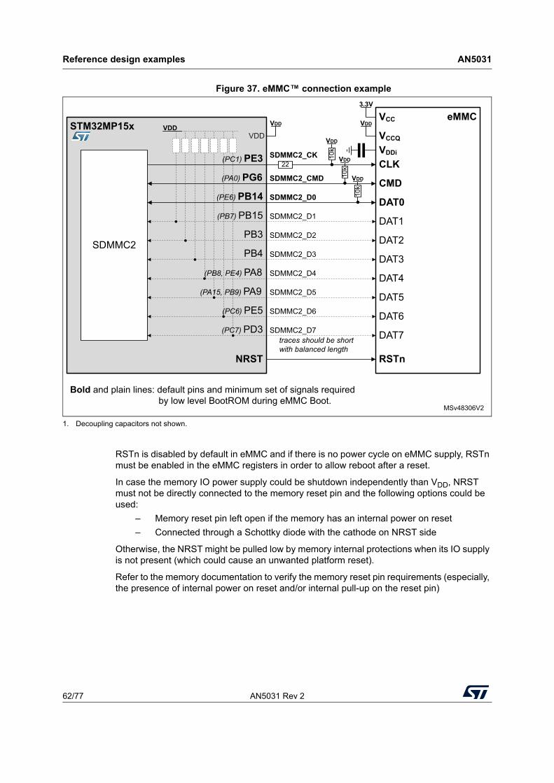
Reference design examples AN5031
62/77 AN5031 Rev 2
Figure 37. eMMC™ connection example
1. Decoupling capacitors not shown.
RSTn is disabled by default in eMMC and if there is no power cycle on eMMC supply, RSTn must be enabled in the eMMC registers in order to allow reboot after a reset.
In case the memory IO power supply could be shutdown independently than VDD, NRST must not be directly connected to the memory reset pin and the following options could be used:
– Memory reset pin left open if the memory has an internal power on reset
– Connected through a Schottky diode with the cathode on NRST side
Otherwise, the NRST might be pulled low by memory internal protections when its IO supply is not present (which could cause an unwanted platform reset).
Refer to the memory documentation to verify the memory reset pin requirements (especially, the presence of internal power on reset and/or internal pull-up on the reset pin)
STM32MP15x
(PC1) PE3 SDMMC2_CK
(PA0) PG6 SDMMC2_CMD
(PE6) PB14 SDMMC2_D0
(PB7) PB15 SDMMC2_D1
PB3 SDMMC2_D2
PB4 SDMMC2_D3
VDD
SDMMC2
10k
VDD
eMMC
Bold and plain lines: default pins and minimum set of signals required by low level BootROM during eMMC Boot.
CMD
DAT0
DAT1
DAT2
DAT3
CLK
RSTn
SDMMC2_D4
(PA15, PB9) PA9 SDMMC2_D5
(PC6) PE5 SDMMC2_D6
(PC7) PD3 SDMMC2_D7
(PB8, PE4) PA8
NRST
DAT4
DAT5
DAT6
DAT7
3.3V
VCC
VCCQ
VDD
MSv48306V2
22
VDD
VDD
traces should be short
with balanced length
VDDi
10k
VDD
10k
VDD
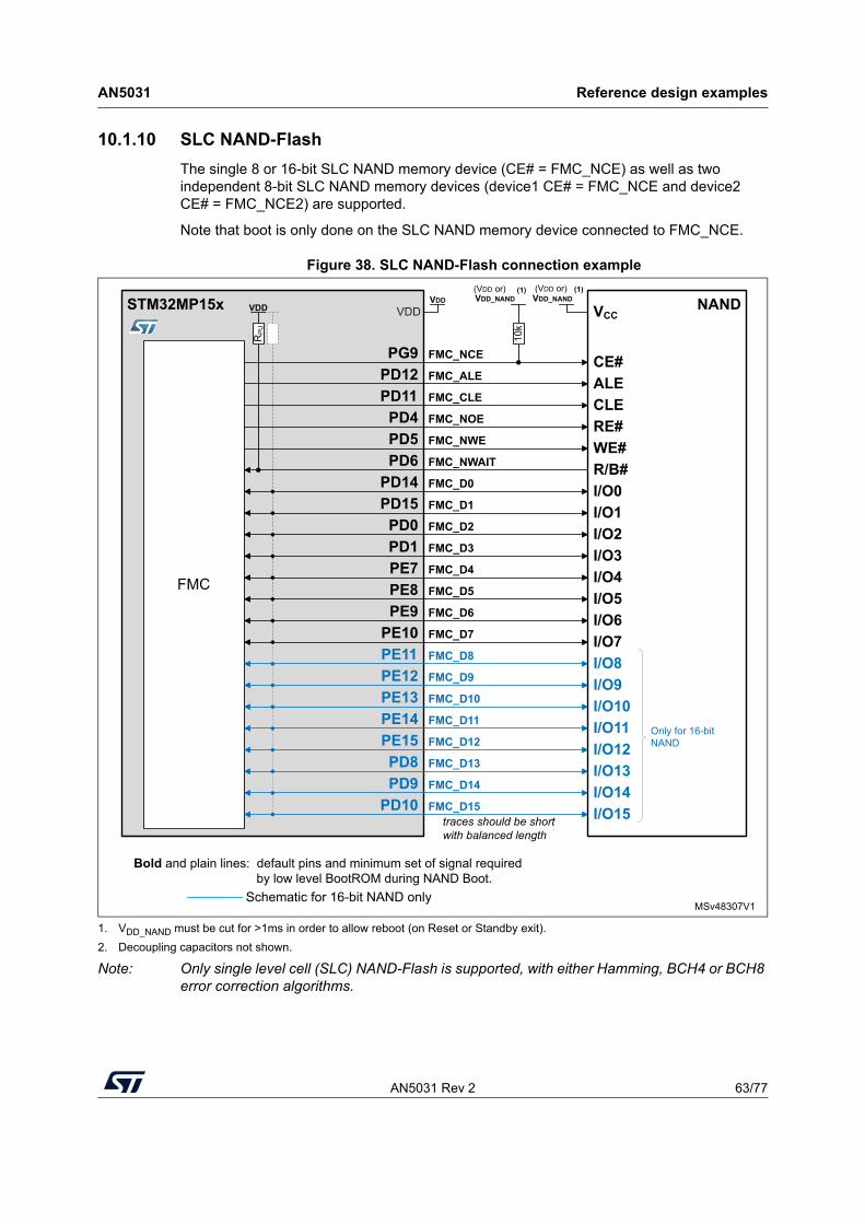
AN5031 Rev 2 63/77
AN5031 Reference design examples
76
10.1.10 SLC NAND-Flash
The single 8 or 16-bit SLC NAND memory device (CE# = FMC_NCE) as well as two independent 8-bit SLC NAND memory devices (device1 CE# = FMC_NCE and device2 CE# = FMC_NCE2) are supported.
Note that boot is only done on the SLC NAND memory device connected to FMC_NCE.
Figure 38. SLC NAND-Flash connection example
1. VDD_NAND must be cut for >1ms in order to allow reboot (on Reset or Standby exit).
2. Decoupling capacitors not shown.
Note: Only single level cell (SLC) NAND-Flash is supported, with either Hamming, BCH4 or BCH8 error correction algorithms.
STM32MP15x
PD12 FMC_ALE
PD11 FMC_CLE
FMC
PG9 FMC_NCE
PD14 FMC_D0
PD15 FMC_D1
PD0 FMC_D2
PD1 FMC_D3
PE7 FMC_D4
PE8 FMC_D5
PE9 FMC_D6
PE10 FMC_D7
PE11 FMC_D8
PE12 FMC_D9
PE13 FMC_D10
PE14 FMC_D11
PE15 FMC_D12
PD8 FMC_D13
PD9 FMC_D14
PD10 FMC_D15
PD4 FMC_NOE
PD5 FMC_NWE
PD6 FMC_NWAIT
Bold and plain lines: default pins and minimum set of signal required by low level BootROM during NAND Boot.
VDD_NAND
VDDVDD
traces should be short
with balanced length
(VDD or) (VDD or)
NAND
ALECLE
CE#
I/O0I/O1I/O2I/O3
I/O5I/O6
I/O4
I/O7I/O8I/O9I/O10I/O11
I/O13I/O14
I/O12
I/O15
RE#WE#R/B#
Only for 16-bit NAND
VCC
MSv48307V1
10k
RP
U
VDDVDD_NAND
(1) (1)
Schematic for 16-bit NAND only
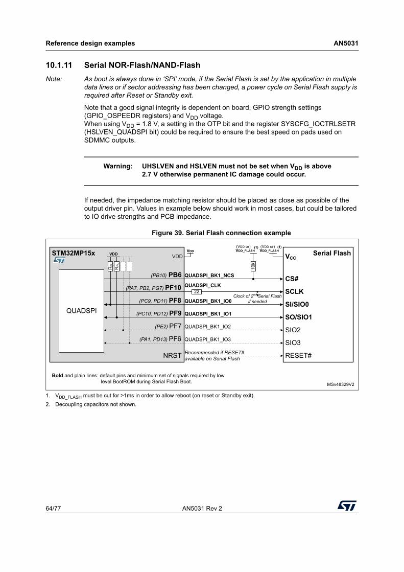
Reference design examples AN5031
64/77 AN5031 Rev 2
10.1.11 Serial NOR-Flash/NAND-Flash
Note: As boot is always done in ‘SPI’ mode, if the Serial Flash is set by the application in multiple data lines or if sector addressing has been changed, a power cycle on Serial Flash supply is required after Reset or Standby exit.
Note that a good signal integrity is dependent on board, GPIO strength settings (GPIO_OSPEEDR registers) and VDD voltage. When using VDD = 1.8 V, a setting in the OTP bit and the register SYSCFG_IOCTRLSETR (HSLVEN_QUADSPI bit) could be required to ensure the best speed on pads used on SDMMC outputs.
Warning: UHSLVEN and HSLVEN must not be set when VDD is above 2.7 V otherwise permanent IC damage could occur.
If needed, the impedance matching resistor should be placed as close as possible of the output driver pin. Values in example below should work in most cases, but could be tailored to IO drive strengths and PCB impedance.
Figure 39. Serial Flash connection example
1. VDD_FLASH must be cut for >1ms in order to allow reboot (on reset or Standby exit).
2. Decoupling capacitors not shown.
STM32MP15x
(PB10) PB6 QUADSPI_BK1_NCS
(PA7, PB2, PG7) PF10 QUADSPI_CLK
(PC9, PD11) PF8 QUADSPI_BK1_IO0
(PC10, PD12) PF9 QUADSPI_BK1_IO1
(PE2) PF7 QUADSPI_BK1_IO2
(PA1, PD13) PF6 QUADSPI_BK1_IO3
VDD
RP
U
QUADSPI
RP
U
10k
VDD_FLASH Serial Flash
Bold and plain lines: default pins and minimum set of signals required by low level BootROM during Serial Flash Boot.
SCLK
SI/SIO0
SO/SIO1
SIO2
SIO3
CS#
RESET#NRST
VDD_FLASH
VCC
MSv48329V2
22
VDDVDD
Clock of 2nd
Serial Flash
if needed
Recommended if RESET#
available on Serial Flash
(VDD or) (VDD or)(1) (1)
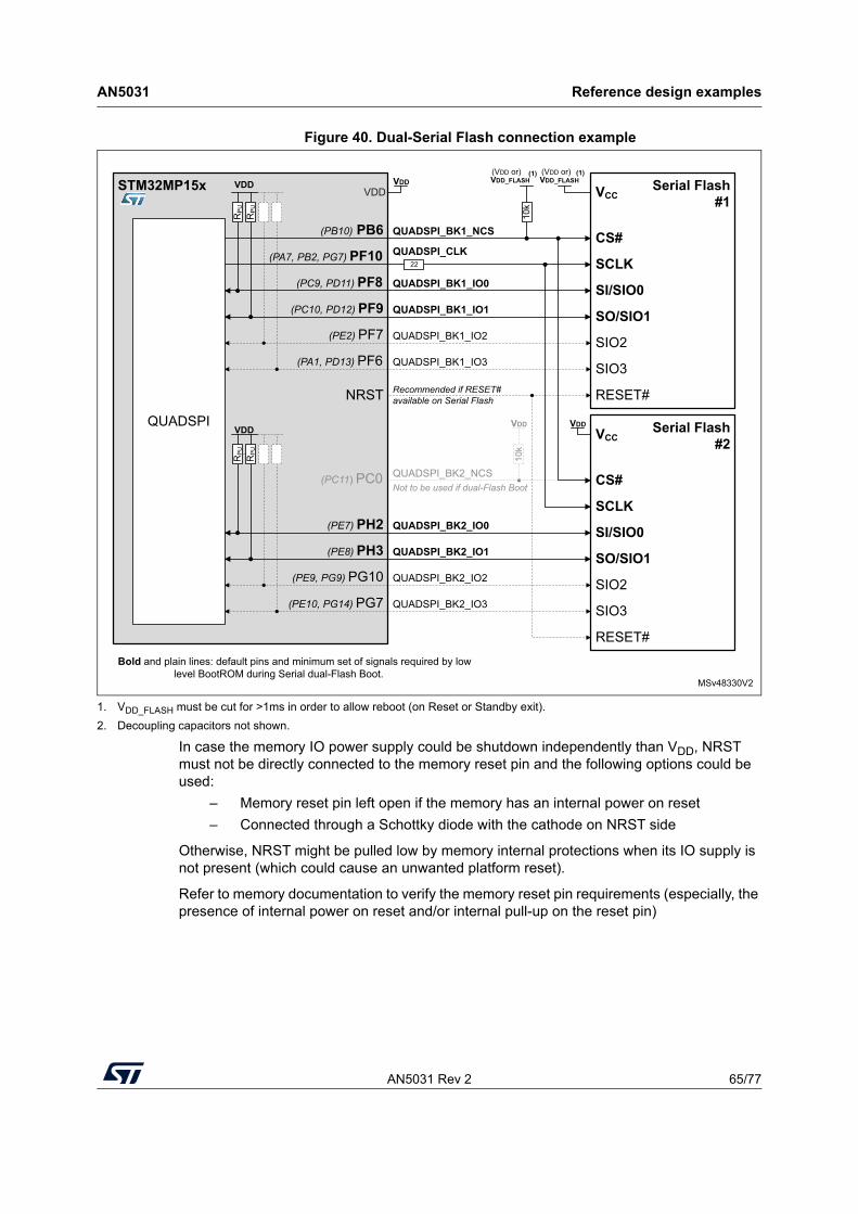
AN5031 Rev 2 65/77
AN5031 Reference design examples
76
Figure 40. Dual-Serial Flash connection example
1. VDD_FLASH must be cut for >1ms in order to allow reboot (on Reset or Standby exit).
2. Decoupling capacitors not shown.
In case the memory IO power supply could be shutdown independently than VDD, NRST must not be directly connected to the memory reset pin and the following options could be used:
– Memory reset pin left open if the memory has an internal power on reset
– Connected through a Schottky diode with the cathode on NRST side
Otherwise, NRST might be pulled low by memory internal protections when its IO supply is not present (which could cause an unwanted platform reset).
Refer to memory documentation to verify the memory reset pin requirements (especially, the presence of internal power on reset and/or internal pull-up on the reset pin)
STM32MP15x
(PB10) PB6 QUADSPI_BK1_NCS
(PA7, PB2, PG7) PF10 QUADSPI_CLK
(PC9, PD11) PF8 QUADSPI_BK1_IO0
(PC10, PD12) PF9 QUADSPI_BK1_IO1
(PE2) PF7 QUADSPI_BK1_IO2
(PA1, PD13) PF6 QUADSPI_BK1_IO3
VDD
RP
U
QUADSPI
RP
U
10k
Serial Flash#1
Bold and plain lines: default pins and minimum set of signals required by low level BootROM during Serial dual-Flash Boot.
SCLK
SI/SIO0
SO/SIO1
SIO2
SIO3
CS#
NRST
VCC
MSv48330V2
22
VDDVDD
(PE7) PH2 QUADSPI_BK2_IO0
(PE8) PH3 QUADSPI_BK2_IO1
(PE9, PG9) PG10 QUADSPI_BK2_IO2
(PE10, PG14) PG7 QUADSPI_BK2_IO3
Serial Flash#2
SCLK
SI/SIO0
SO/SIO1
SIO2
SIO3
CS#
VDD
VCC
(PC11) PC0 QUADSPI_BK2_NCS
RESET#
RESET#
VDD
RP
U
RP
U
10k
VDD
Recommended if RESET#
available on Serial Flash
Not to be used if dual-Flash Boot
VDD_FLASH VDD_FLASH(VDD or) (VDD or)(1) (1)
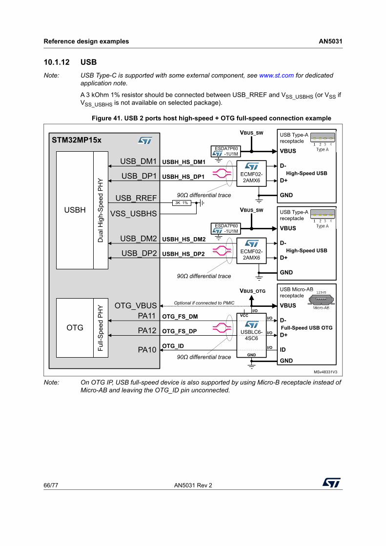
Reference design examples AN5031
66/77 AN5031 Rev 2
10.1.12 USB
Note: USB Type-C is supported with some external component, see www.st.com for dedicated application note.
A 3 kOhm 1% resistor should be connected between USB_RREF and VSS_USBHS (or VSS if VSS_USBHS is not available on selected package).
Figure 41. USB 2 ports host high-speed + OTG full-speed connection example
Note: On OTG IP, USB full-speed device is also supported by using Micro-B receptacle instead of Micro-AB and leaving the OTG_ID pin unconnected.
STM32MP15x
USBH
USB_DM1 USBH_HS_DM1
VBUS_SW
USB_DP1 USBH_HS_DP1
MSv48331V3
ECMF02-2AMX6
USB Type-A receptacle
A
D-
VBUS
D+
GND
USB_DM2 USBH_HS_DM2
USB_DP2 USBH_HS_DP2
90Ω differential trace
ECMF02-2AMX6
USB Type-A receptacle
A
D-
VBUS
D+
GND
OTGPA11 OTG_FS_DM
VBUS_OTG
PA12 OTG_FS_DP
OTG_VBUS
PA10
USBLC6-4SC6
USB Micro-AB receptacle
AB
D-
VBUS
D+
GND
IDOTG_ID
3K 1%USB_RREF
Dua
l Hig
h-S
peed
PH
YFu
ll-S
peed
PH
Y
High-Speed USB
High-Speed USB
Full-Speed USB OTG
90Ω differential trace
VBUS_SW
I/O
I/O
I/O
I/OVCC
GND
VSS_USBHS
90Ω differential trace
ESDA7P60-1U1M
ESDA7P60-1U1M
Optional if connected to PMIC
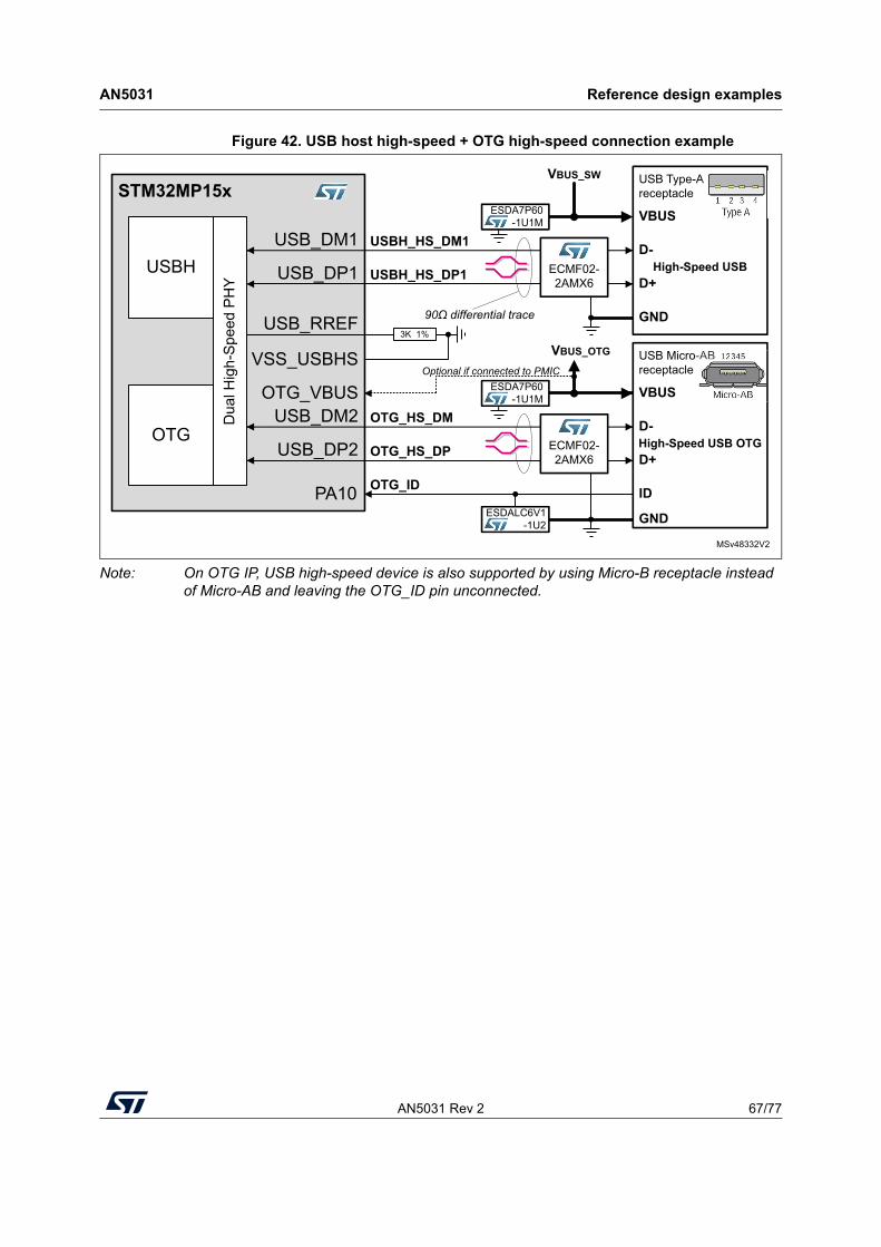
AN5031 Rev 2 67/77
AN5031 Reference design examples
76
Figure 42. USB host high-speed + OTG high-speed connection example
Note: On OTG IP, USB high-speed device is also supported by using Micro-B receptacle instead of Micro-AB and leaving the OTG_ID pin unconnected.
STM32MP15x
USBHUSB_DM1 USBH_HS_DM1
USB_DP1 USBH_HS_DP1
MSv48332V2
ECMF02-2AMX6
USB Type-A receptacle
A
D-
VBUS
D+
GND
OTG_HS_DM
OTG_HS_DP
OTG_VBUS
PA10
ECMF02-2AMX6
USB Micro-AB receptacle
-AB
D-
VBUS
D+
GND
IDOTG_ID
3K 1%USB_RREF
Dua
l Hig
h-S
peed
PH
Y
High-Speed USB
High-Speed USB OTGOTGUSB_DM2
USB_DP2
VBUS_SW
VBUS_OTG VSS_USBHS
90Ω differential trace
ESDA7P60-1U1M
ESDA7P60-1U1M
ESDALC6V1-1U2
Optional if connected to PMIC
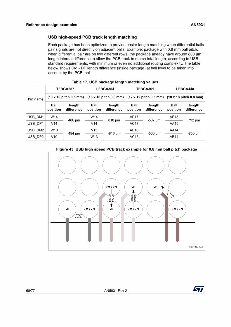
Reference design examples AN5031
68/77 AN5031 Rev 2
USB high-speed PCB track length matching
Each package has been optimized to provide easier length matching when differential balls pair signals are not directly on adjacent balls. Example: package with 0.8 mm ball pitch, when differential pair are on two different rows, the package already have around 800 µm length internal difference to allow the PCB track to match total length, according to USB standard requirements, with minimum or even no additional routing complexity. The table below shows DM - DP length difference (inside package) at ball level to be taken into account by the PCB tool.
Figure 43. USB high speed PCB track example for 0.8 mm ball pitch package
Table 17. USB package length matching values
Pin name
TFBGA257 LFBGA354 TFBGA361 LFBGA448
(10 x 10 pitch 0.5 mm) (16 x 16 pitch 0.8 mm) (12 x 12 pitch 0.5 mm) (18 x 18 pitch 0.8 mm)
Ball position
length difference
Ball position
length difference
Ball position
length difference
Ball position
length difference
USB_DM1 W14486 µm
W14818 µm
AB17-507 µm
AB15792 µm
USB_DP1 V14 V14 AC17 AA15
USB_DM2 W10494 µm
V13-816 µm
AB16-500 µm
AA14-850 µm
USB_DP2 V10 W13 AC16 AB14
xM / xN
xP
xP
xM / xN
xP
xM / xN
-800
μm
-500
μm
800
μm50
0 μm
1131 μm707 μm
Length match
xP xM / xN
MSv48333V2
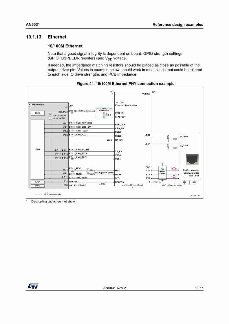
AN5031 Rev 2 69/77
AN5031 Reference design examples
76
10.1.13 Ethernet
10/100M Ethernet
Note that a good signal integrity is dependent on board, GPIO strength settings (GPIO_OSPEEDR registers) and VDD voltage.
If needed, the impedance matching resistors should be placed as close as possible of the output driver pin. Values in example below should work in most cases, but could be tailored to each side IO drive strengths and PCB impedance.
Figure 44. 10/100M Ethernet PHY connection example
1. Decoupling capacitors not shown.
STM32MP15x
PA1
ETH
ETH1_RMII_REF_CLK
PA7 ETH1_RMII_CRS_DV
PC4 ETH1_RMII_RXD0
PC5 ETH1_RMII_RXD1
(PB12) PG13 ETH1_RMII_TXD0
(PB13) PG14 ETH1_RMII_TXD1
PC1 ETH1_MDC
PA2 ETH1_MDIOPG12 ETH1_PHY_INTN
(PG11) PB11 ETH1_RMII_TX_EN
PB5, PG8 ETH_CLK (25 MHz Reference)RCC
Pxx GPIOxxGPIO
VDD
Pxx WKUPxPWR optional
VDD1k5
VDD1k5
Pull-up should
be set by SW
22
22
22
22PHYAD[2:0] = 0b001
22
VDDVDD
VDD
optional if RCC provides a 25 MHz clock
25M
Hz
10/100M Ethernet Transceiver
RX_ERopen
XTAL_OUT
XTAL_IN
REF_CLK
RESETn
INTn
TX_EN
MDIO
TXD0
TXD1
CRS_DV
RXD0
RXD1
MDC RJ45 connector with Magnetics
and LEDs
270
4k7 Yellow
1%
TXP
TXN
RXP
RXN
LED0
LED1
Rexposed thermal pad 100Ω differential traces
USBLC6-4SC6
3.3V
270
4k7 Green
10k
3.3VVDD3V3
MSv48334V1Optional schematic
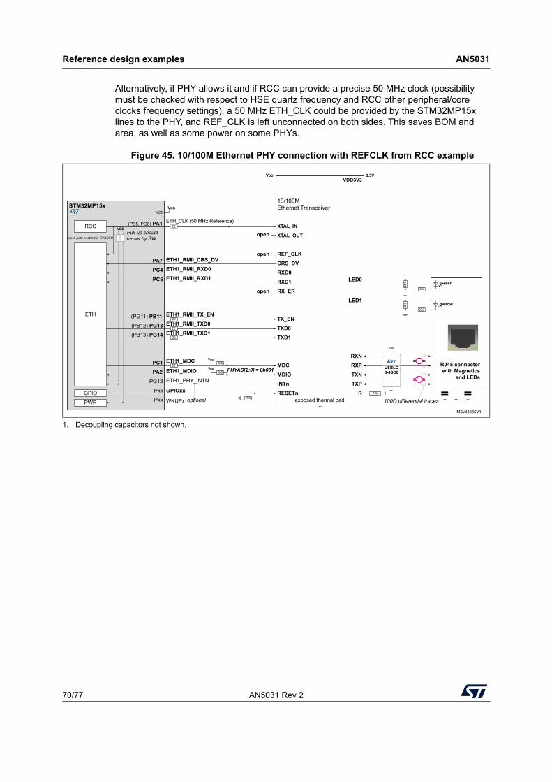
Reference design examples AN5031
70/77 AN5031 Rev 2
Alternatively, if PHY allows it and if RCC can provide a precise 50 MHz clock (possibility must be checked with respect to HSE quartz frequency and RCC other peripheral/core clocks frequency settings), a 50 MHz ETH_CLK could be provided by the STM32MP15x lines to the PHY, and REF_CLK is left unconnected on both sides. This saves BOM and area, as well as some power on some PHYs.
Figure 45. 10/100M Ethernet PHY connection with REFCLK from RCC example
1. Decoupling capacitors not shown.
STM32MP15x
ETH
PA7 ETH1_RMII_CRS_DV
PC4 ETH1_RMII_RXD0
PC5 ETH1_RMII_RXD1
(PB12) PG13 ETH1_RMII_TXD0
(PB13) PG14 ETH1_RMII_TXD1
PC1 ETH1_MDC
PA2 ETH1_MDIO
PG12 ETH1_PHY_INTN
(PG11) PB11 ETH1_RMII_TX_EN
(PB5, PG8) PA1 ETH_CLK (50 MHz Reference)RCC
Pxx GPIOxxGPIO
VDD
Pxx WKUPxPWR optional
VDD1k5
VDD1k5
Pull-up should
be set by SW
22
22
22
22PHYAD[2:0] = 0b001
VDDVDD
VDD
10/100M Ethernet Transceiver
RX_ERopen
XTAL_OUT
XTAL_IN
REF_CLK
RESETn
INTn
TX_EN
MDIO
TXD0
TXD1
CRS_DV
RXD0
RXD1
MDC RJ45 connector with Magnetics
and LEDs
270
4k7 Yellow
1%
TXP
TXN
RXP
RXN
LED0
LED1
Rexposed thermal pad 100Ω differential traces
USBLC6-4SC6
3.3V
270
4k7 Green
10k
3.3VVDD3V3
MSv48335V1
open
open
clock path enabled in SYSCFG
22

AN5031 Rev 2 71/77
AN5031 Reference design examples
76
Gigabit Ethernet
Note that a good signal integrity is dependent on board, GPIO strength settings (GPIO_OSPEEDR registers) and VDD voltage. When using VDD = 1.8 V, a setting in the OTP bit and the register SYSCFG_IOCTRLSETR (HSLVEN_ETH bit) is required to ensure the best speed on pads used on Ethernet outputs.
Warning: UHSLVEN must not be set when VDD is above 2.7 V otherwise permanent IC damage could occur.
If needed, the impedance matching resistors should be placed as close as possible of the output driver pin. Values in example below should work in most cases, but could be tailored to each side IO drive strengths and PCB impedance.
Figure 46. Gigabit Ethernet PHY connection example with VDD = 3.3 V (RTL8211E)
1. Decoupling capacitors not shown.
RJ45 connector with Magnetics
and LEDs
PHY_AD2=0
STM32MP15x
PG5
PA1
ETH
3.3V
ETH1_RGMII_CLK125
ETH1_RGMII_RX_CLK
PA7 ETH1_RGMII_RX_CTL
PC4 ETH1_RGMII_RXD0
(PH7) PB1 ETH1_RGMII_RXD3
PC5 ETH1_RGMII_RXD1
(PH6) PB0 ETH1_RGMII_RXD2
PG4 ETH1_RGMII_GTX_CLK
(PB12) PG13 ETH1_RGMII_TXD0
(PB13) PG14 ETH1_RGMII_TXD1
PC2 ETH1_RGMII_TXD2
(PB8) PE2 ETH1_RGMII_TXD3
PC1 ETH1_MDC
PA2 ETH1_MDIO
PG12 ETH1_PHY_INTN
(PG11) PB11 ETH1_RGMII_TX_CTL
PB5, PG8 ETH_CLK (25 MHz Reference)RCC
optional if RCC
provides a
25 MHz clock
Green
510
4k7 Yellow
510
4k7 Green
3.3V
PHY_AD0=1
PHY_AD1=0
RXDLY = 14k73.3V4k7
SELRGV=1
3.3V4k7
TXDLY=1
4k7TXDLY=0
or
3.3V4k7
AN0=1
3.3V4k7
AN1=1
25M
Hz
10k
Pxx GPIOxxGPIO
VDD
Pxx WKUPxPWRoptional
3.3V
AVDD10 (1.05V)
15, 21
44, 45
48
3
9, 40
28, 36
4k73.3V
47
3.3V
6, 41
MSv48338V1
42
43
46
19
13
14
16
17
18
22
27
23
24
25
26
30
31
20
29
33
38
32
34
35
11
10
8
7
5
4
2
1
39
RTL8211E-VB-CG(48-pin QFN)10/100/1000M Ethernet Transceiver
CLK125
RXC
RXCTL
RXD0
RXD3
RXD1
RXD2
TXC
TXD0
TXD1
TXD2
TXD3
MDC
MDIO
INTB
TXCTL
CKXTAL2
CKXTAL1
MDI0P
MDI0N
MDI1P
MDI1N
MDI2P
MDI2N
MDI3P
MDI3N
LED0
LED1
LED2
PHYRSTB
PMEB
RSET
DVDD3V3 (VIO)
VDDREG
REG_OUT
AVDD10
AVDD10
DVDD10
ENSWREG
GND exposed thermal pad
AVDD3V3
510
4k7
3.3V
12NC
3.3V1k5
3.3V1k5
Pull-up should
be set by SW
49
22
22
22
22
22
22
22
22
22
22
22
22
22
22
PHY_AD[2:0] = 0b001
22
50Ω traces unless otherwise noted
100Ω differential traces
traces should be short with balanced length
VDDVDD
2 x HSP051-
4M10
2k49 1%
510
4k7 Green
RXDLY = 0
or
(PHY_AD1)
(PHY_AD2)
(RXDLY)
(TXDLY)
(PHY_AD0)
(SELRGV)
(AN0)
(AN1)
37DVDD3V3
125 MHz
clock path enabled in SYSCFG
or
oroptional if RCC 125 MHz is available
VDD = 3.3V ± 5% (PHY 3.3V can be shutdown during STANDBY)
Optional schematic
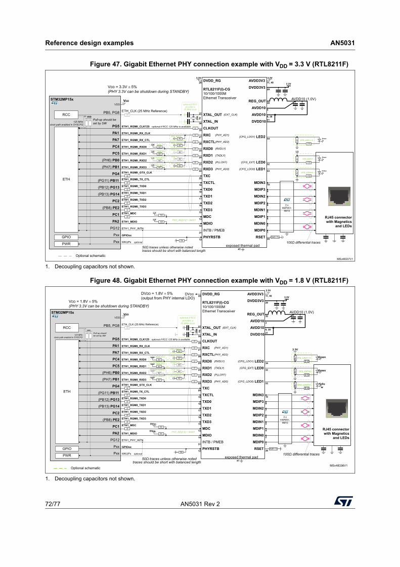
Reference design examples AN5031
72/77 AN5031 Rev 2
Figure 47. Gigabit Ethernet PHY connection example with VDD = 3.3 V (RTL8211F)
1. Decoupling capacitors not shown.
Figure 48. Gigabit Ethernet PHY connection example with VDD = 1.8 V (RTL8211F)
1. Decoupling capacitors not shown.
PHY_AD2=0
RJ45 connector with Magnetics
and LEDs
STM32MP15x
PG5
PA1
ETH
3.3V
ETH1_RGMII_CLK125
ETH1_RGMII_RX_CLK
PA7 ETH1_RGMII_RX_CTL
PC4 ETH1_RGMII_RXD0
(PH7) PB1 ETH1_RGMII_RXD3
PC5 ETH1_RGMII_RXD1
(PH6) PB0 ETH1_RGMII_RXD2
PG4 ETH1_RGMII_GTX_CLK
(PB12) PG13 ETH1_RGMII_TXD0
(PB13) PG14 ETH1_RGMII_TXD1
PC2 ETH1_RGMII_TXD2
(PB8) PE2 ETH1_RGMII_TXD3
PC1 ETH1_MDC
PA2 ETH1_MDIO
PG12 ETH1_PHY_INTN
(PG11) PB11 ETH1_RGMII_TX_CTL
PB5, PG8 ETH_CLK (25 MHz Reference)RCC
optional if RCC
provides a
25 MHz clock
Green
510
4k7 Yellow
510
4k7 Green
CFG_LDO1 = 0
CFG_EXT=1
CFG_LDO0=0
4k73.3V4k7
RXDLY=1
3.3V4k7
TXDLY=1
4k7TXDLY=0
or
3.3V
4k7PLLOFF=1
3.3V4k7
PHY_AD0=1
25M
Hz
10k
Pxx GPIOxxGPIO
VDD
Pxx WKUPxPWR optional
2k49 1%
3.3V
AVDD10 (1.0V)
28
29
30
3
8, 3821
3.3V
11, 40
MSv48337V1
37
36
35
27
26
25
24
23
22
20
19
18
17
16
15
13
14
31
12
34
32
33
10
9
7
6
5
4
2
1
39
RTL8211F(I)-CG10/100/1000M Ethernet Transceiver
CLKOUT
RXC
RXCTL
RXD0
RXD3
RXD1
RXD2
TXC
TXD0
TXD1
TXD2
TXD3
MDC
MDIO
INTB / PMEB
TXCTL
XTAL_IN
XTAL_OUT
MDIP0
MDIN0
MDIP1
MDIN1
MDIP2
MDIN2
MDIP3
MDIN3
LED0
LED1
LED2
PHYRSTB RSET
DVDD_RG
DVDD3V3
REG_OUT
AVDD10
AVDD10
DVDD10
exposed thermal pad
AVDD3V3
510
4k7
3.3VRXDLY=0
4k7
or
3.3V1k5
3.3V1k5
Pull-up should be
set by SW
41
22
22
22
22
22
22
22
22
22
22
22
22
22
22
PHY_AD[2:0] = 0b001
22
traces should be short with balanced length
100Ω differential traces
PHY_AD1=04k7
4k7PLLOFF=0
or
2 x HSP051-
4M10
(PHY_AD1)
(PHY_AD2)
(RXDLY)
(PHY_AD0)
(TXDLY)
(PLLOFF)
(EXT_CLK)
(CFG_EXT)
(CFG_LDO0)
(CFG_LDO1)
VDDVDD
50Ω traces unless otherwise noted
125 MHz
clock path enabled in SYSCFG
or
or optional if RCC 125 MHz is available
VDD = 3.3V ± 5% (PHY 3.3V can be shutdown during STANDBY)
Optional schematic
PHY_AD2=0
RJ45 connector with Magnetics
and LEDs
STM32MP15x
PG5
PA1
ETH
DVDD
ETH1_RGMII_CLK125
ETH1_RGMII_RX_CLK
PA7 ETH1_RGMII_RX_CTL
PC4 ETH1_RGMII_RXD0
(PH7) PB1 ETH1_RGMII_RXD3
PC5 ETH1_RGMII_RXD1
(PH6) PB0 ETH1_RGMII_RXD2
PG4 ETH1_RGMII_GTX_CLK
(PB12) PG13 ETH1_RGMII_TXD0
(PB13) PG14 ETH1_RGMII_TXD1
PC2 ETH1_RGMII_TXD2
(PB8) PE2 ETH1_RGMII_TXD3
PC1 ETH1_MDC
PA2 ETH1_MDIO
PG12 ETH1_PHY_INTN
(PG11) PB11 ETH1_RGMII_TX_CTL
PB5, PG8 ETH_CLK (25 MHz Reference)RCC
optional if RCC
provides a
25 MHz clock
510
4k7 Yello
w
510
4k7 Green
3.3V
CFG_LDO0=0
CFG_LDO1 =14k7DVDD4k7
RXDLY=1
DVDD4k7
TXDLY=1
4k7TXDLY=0
or
DVDD
4k7PLLOFF=1
DVDD4k7
PHY_AD0=1
25M
Hz
10k
Pxx GPIOxxGPIO
VDD
Pxx WKUPxPWR optional
2k49 1%
3.3V
AVDD10 (1.0V)
28
29
30
3
8, 3821
3.3V
11, 40
MSv48336V1
37
36
35
27
26
25
24
23
22
20
19
18
17
16
15
13
14
31
12
34
32
33
10
9
7
6
5
4
2
1
39
RTL8211F(I)-CG10/100/1000M Ethernet Transceiver
CLKOUT
RXC
RXCTL
RXD0
RXD3
RXD1
RXD2
TXC
TXD0
TXD1
TXD2
TXD3
MDC
MDIO
INTB / PMEB
TXCTL
XTAL_IN
XTAL_OUT
MDIP0
MDIN0
MDIP1
MDIN1
MDIP2
MDIN2
MDIP3
MDIN3
LED0
LED1
LED2
PHYRSTB RSET
DVDD_RG
DVDD3V3
REG_OUT
AVDD10
AVDD10
DVDD10
exposed thermal pad
AVDD3V3
RXDLY=04k7
or
DVDD1k5
DVDD1k5
Pull-up should
be set by SW
41
22
22
22
22
22
22
22
22
22
22
22
22
22
22
PHY_AD[2:0] = 0b001
22
traces should be short with balanced length
100Ω differential traces
PHY_AD1=04k7
4k7PLLOFF=0
or
2 x HSP051-
4M10
(PHY_AD1)
(PHY_AD2)
(RXDLY)
(PHY_AD0)
(TXDLY)
(PLLOFF)
(EXT_CLK)
(CFG_EXT)
(CFG_LDO0)
(CFG_LDO1)
VDDVDD
50Ω traces unless otherwise noted
125 MHz
clock path enabled in SYSCFG
or
or optional if RCC 125 MHz is available
510
4k7 GreenCFG_EXT=0
VDD = 1.8V ± 5% (PHY 3.3V can be shutdown during STANDBY)
DVDD = 1.8V ± 5% (output from PHY internal LDO)
Optional schematic
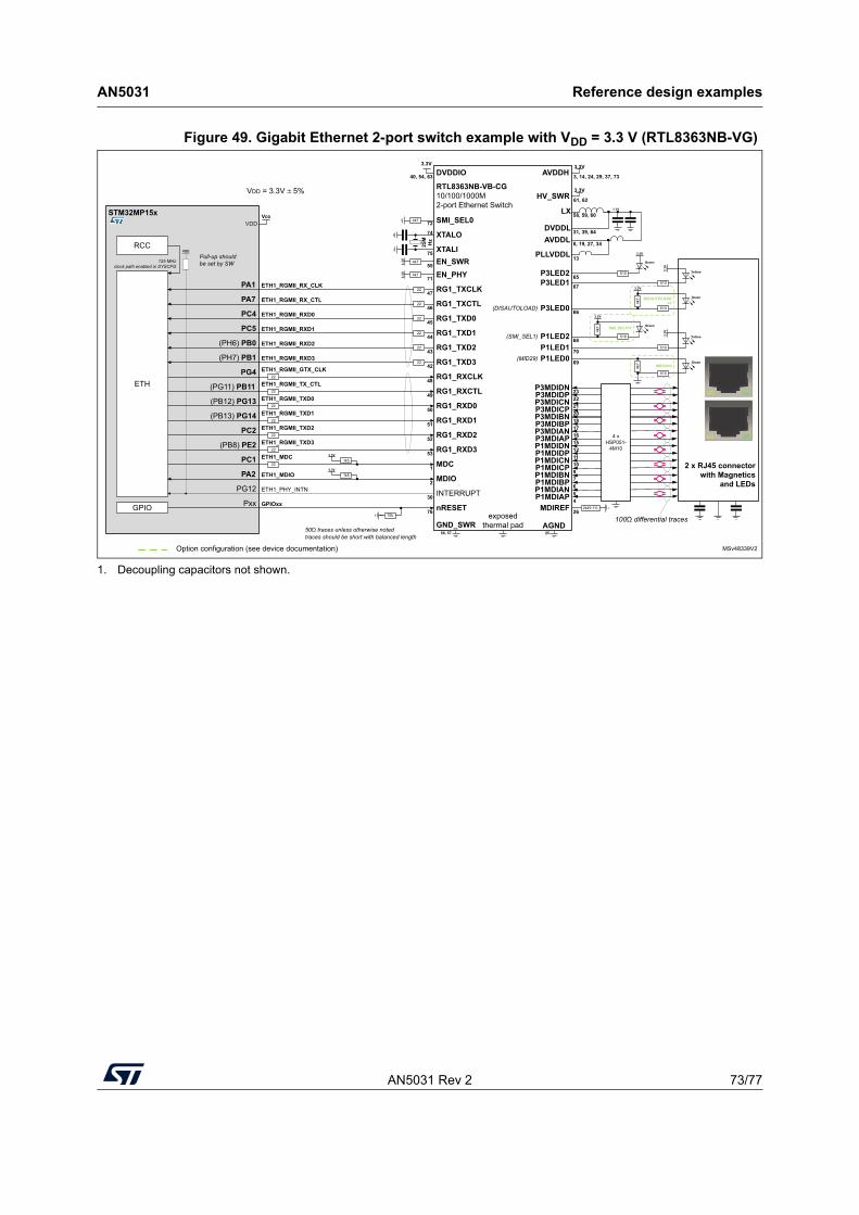
AN5031 Rev 2 73/77
AN5031 Reference design examples
76
Figure 49. Gigabit Ethernet 2-port switch example with VDD = 3.3 V (RTL8363NB-VG)
1. Decoupling capacitors not shown.
2 x RJ45 connector with Magnetics
and LEDs
STM32MP15x
PA1
ETH
3.3V
ETH1_RGMII_RX_CLK
PA7 ETH1_RGMII_RX_CTL
PC4 ETH1_RGMII_RXD0
(PH7) PB1 ETH1_RGMII_RXD3
PC5 ETH1_RGMII_RXD1
(PH6) PB0 ETH1_RGMII_RXD2
PG4 ETH1_RGMII_GTX_CLK
(PB12) PG13 ETH1_RGMII_TXD0
(PB13) PG14 ETH1_RGMII_TXD1
PC2 ETH1_RGMII_TXD2
(PB8) PE2 ETH1_RGMII_TXD3
PC1 ETH1_MDC
PA2 ETH1_MDIO
PG12 ETH1_PHY_INTN
(PG11) PB11 ETH1_RGMII_TX_CTL
RCC
Yellow
510
4k7 Green
510
4k7 Green
3.3V
MID29=0
25M
Hz
10k
Pxx GPIOxxGPIO
VDD
2k49 1%
40, 54, 63
8, 19, 27, 34
31, 39, 64
13
3.3V
3, 14, 24, 29, 37, 73
MSv48339V2
74
75
47
46
45
44
43
42
48
49
50
51
52
53
1
2
30
76
68
70
69
23
21
18
16
12
10
7
5
26
RTL8363NB-VB-CG10/100/1000M 2-port Ethernet Switch
RG1_TXCLK
RG1_TXCTL
RG1_TXD0
RG1_TXD3
RG1_TXD1
RG1_TXD2
RG1_RXCLK
RG1_RXD0
RG1_RXD1
RG1_RXD2
RG1_RXD3
MDC
MDIO
INTERRUPT
RG1_RXCTL
XTALI
XTALO
P1MDIAN
P1MDIBN
P1MDICN
P1MDIDN
P1LED1P1LED0
P1LED2
nRESET MDIREF
DVDDIO
AVDDLDVDDL
PLLVDDL
GND_SWR
AVDDH
510
3.3V
3.3V1k5
3.3V1k5
Pull-up should
be set by SW
56, 57
22
22
22
22
22
22
22
22
22
22
22
22
22
traces should be short with balanced length
100Ω differential traces
(MID29)
VDDVDD
50Ω traces unless otherwise noted
125 MHz
clock path enabled in SYSCFG
VDD = 3.3V ± 5%
AGND25
exposed thermal pad
510
Green
65P3LED2
SMI_SEL1=1
Yellow
Green
67
66
P3LED1
P3LED0
510
(DISAUTOLOAD) 510
DISAUTOLOAD=1
3.3V
3.3V
4k7
22
20
17
15
11
9
6
4P1MDIAP
P1MDIBP
P1MDICP
P1MDIDP
P3MDIAN
P3MDIBN
P3MDICN
P3MDIDN
P3MDIAP
P3MDIBP
P3MDICP
P3MDIDP
(SMI_SEL1)
71 EN_PHY
72 SMI_SEL04k7
4k73.3V
Option configuration (see device documentation)
4 x HSP051-
4M10
55 EN_SWR4k73.3V
3.3V
61, 62HV_SWR
3.3V
58, 59, 60LX 1.1V

Reference design examples AN5031
74/77 AN5031 Rev 2
10.1.14 Display serial interface (DSI)
Figure 50. Display connection example with DSI
1. ECMF04-4HSWM10 includes common mode filter for WLAN/BT bands. For ESD protection only, HSP051-4M10 could be used instead (similar but not same footprint).
2. Decoupling capacitors not shown.
3. Availability of DSI depends on the STM32MP15x lines devices.
STM32MP157
VDDA1V8_REG
VDD1V2_DSI_REG
VDD1V2_DSI_PHY
VDDA1V8_DSI
MSv48340V2
100Ω differential
trace
DSI Display
DSI_TE
DSI_CK_P
DSI_CK_N
DSI_D0_P
DSI_D0_N
DSI_D1_P
DSI_D1_N
DSI
LDO 1.2V
LDO 1.8V
DSI PLL
DS
I PH
Y
100Ω differential
trace
100Ω differential
trace
SuppliesVDD
VDDVDD
2 xECMF04-4HSWM10
Recommended
connection even if DSI
is not used
Recommended
connection even if DSI
is not used
Recommended connections
(1)
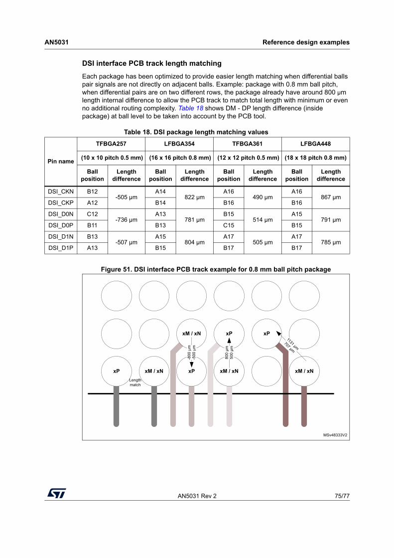
AN5031 Rev 2 75/77
AN5031 Reference design examples
76
DSI interface PCB track length matching
Each package has been optimized to provide easier length matching when differential balls pair signals are not directly on adjacent balls. Example: package with 0.8 mm ball pitch, when differential pairs are on two different rows, the package already have around 800 µm length internal difference to allow the PCB track to match total length with minimum or even no additional routing complexity. Table 18 shows DM - DP length difference (inside package) at ball level to be taken into account by the PCB tool.
Figure 51. DSI interface PCB track example for 0.8 mm ball pitch package
Table 18. DSI package length matching values
Pin name
TFBGA257 LFBGA354 TFBGA361 LFBGA448
(10 x 10 pitch 0.5 mm) (16 x 16 pitch 0.8 mm) (12 x 12 pitch 0.5 mm) (18 x 18 pitch 0.8 mm)
Ball position
Length difference
Ball position
Length difference
Ball position
Length difference
Ball position
Length difference
DSI_CKN B12-505 µm
A14822 µm
A16490 µm
A16867 µm
DSI_CKP A12 B14 B16 B16
DSI_D0N C12-736 µm
A13781 µm
B15514 µm
A15791 µm
DSI_D0P B11 B13 C15 B15
DSI_D1N B13-507 µm
A15804 µm
A17505 µm
A17785 µm
DSI_D1P A13 B15 B17 B17
xM / xN
xP
xP
xM / xN
xP
xM / xN
-800
μm
-500
μm
800
μm50
0 μm
1131 μm707 μm
Length match
xP xM / xN
MSv48333V2
Revision history AN5031
76/77 AN5031 Rev 2
11 Revision history
Table 19. Document revision history
Date Revision Changes
01-Feb-2019 1 Initial release.
14-Apr-2020 2
Updated:
– Cover replacing STM32MP1 Series by STM32MP151, STM32MP153 and STM32MP157 lines.
– Table 1: Reference documents.
– Section 4.1: Introduction USB supplies.
– Section 4.2: Power supply schemes.
– Table 4: Amount of decoupling recommendation by package.
– Figure 8: 12x12 TFBGA361 compatibility.
– Figure 30: Discrete supplies example 3.3 V I/Os with DDR3L.
– Figure 31: PMIC example 3.3 V I/Os with DDR3L
– Figure 41: USB 2 ports host high-speed + OTG full-speed connection example.
– Figure 49: Gigabit Ethernet 2-port switch example with VDD = 3.3 V (RTL8363NB-VG).
Removed:
– ‘ST1S31PUR SMPS details’ figure.
– ‘Components example for 1.2 V 2A’ table.
– ‘Components example for 1.35 V 1A’ table.

AN5031 Rev 2 77/77
AN5031
77
IMPORTANT NOTICE – PLEASE READ CAREFULLY
STMicroelectronics NV and its subsidiaries (“ST”) reserve the right to make changes, corrections, enhancements, modifications, and improvements to ST products and/or to this document at any time without notice. Purchasers should obtain the latest relevant information on ST products before placing orders. ST products are sold pursuant to ST’s terms and conditions of sale in place at the time of order acknowledgement.
Purchasers are solely responsible for the choice, selection, and use of ST products and ST assumes no liability for application assistance or the design of Purchasers’ products.
No license, express or implied, to any intellectual property right is granted by ST herein.
Resale of ST products with provisions different from the information set forth herein shall void any warranty granted by ST for such product.
ST and the ST logo are trademarks of ST. For additional information about ST trademarks, please refer to www.st.com/trademarks. All other product or service names are the property of their respective owners.
Information in this document supersedes and replaces information previously supplied in any prior versions of this document.
© 2020 STMicroelectronics – All rights reserved
Recommended