Electronics The Seventh and Eighth and Lectures
Eighth weekهـ - 1436/ 12 / 28
هـ 1437/ 1 / 1
السلمي / سمر أ

Chapter Two: Junction Diode Physical Electronics Forward-biased and Reverse- biased Junction
depletion region and applying bias, and Diffusion and Drift currentsDrive excess of minority carrier in Forward-biased and Reverse- biased
Junction Mathematical description of excess of minority carrier in Forward-biased
and Reverse- biased JunctionDrive diffusion current in forward-biased and reverse- biased JunctionI – V characteristic of forward-biased and reverse-biased JunctionDiode ModelsPn Junction’s mission(half and full wave rectifiers, filters, regulator)Zener diode
Ohmic Contact Metal–Oxide–Semiconductor Contact (MOS) Structure , Effect of voltageEnergy levels forms in MOS in different bias
Outline for today

Time of Periodic Exams
The first periodic exam in / 1 / 1437 - 1312هـ , Please everyone attend In her
group
The second homework
I put the second homework in my website in the university homework Due
Thursday 2 / 1/ 1437 H in my mailbox in Faculty of Physics Department , I will
not accept any homework after that , but if you could not come to university you
should sent it to me by email in the same day

Forward-biased and Reverse- biased JunctionOur discussion until now is about equilibrium condition (The absence of power supply (battery) between the parties of diode).
But what about the condition (the existence of power supply between the parties of diode?How the power supply connect between the parties of the diode ?? What happens to contact potential increased or decreased?What will happened to diffusion and drift currents in the junction?
In the condition of power supply existence, so that positive terminal of it connect with p-type side and negative terminal of it connect with n-type side; this condition called forward bias. however, If the two terminals reverse, the condition called reverse bias as in the figure blow.
=

Forward-biased Junction (depletion region and applying bias)
In forward bias, we notice that the outer field (forward voltage) opposes built-in
field created by the space charges in the depletion region. Therefore, the number
of donor and acceptor ions reduces; thus depletion region width decreases. The
potential barrier is lower in this condition than in equilibrium condition; in
addition voltage difference across the diode decreases (( V0 –Vf )) as in the figure.
Also we notice that Fermi level will not be at the same energy level in the two
types as in equilibrium condition.

Forward-biased Junction (Diffusion and Drift)
This decreasing of voltage difference across the diode in forward bias affect the
diffusion current ( due to injection of holes in p-type and electrons in n-type ) so,
we obtain a huge flow of diffusion currents of the electrons and holes compared
with it in equilibrium condition ; also due to climbing of electron easily to new
voltage difference level .
However, drift current is not effected by decreasing of voltage difference or
length of potential barrier due to not effecting of minority carrier which remain
pulled inside the diffusion current at the edge of the depletion region . Therefore,
drift current in this condition remains as in equilibrium condition

Reverse-biased Junction (depletion region and applying bias)
In reverse bias, we notice that the outer field (reverse voltage ) in the same
direction of built-in field created by the space charges in the depletion region.
Therefore, the number of donor and acceptor ions rise; thus depletion region
width increases. The potential barrier is higher in this condition than in
equilibrium condition; in addition voltage difference across the diode increases
((V0 + Vr )) as in the figure. Also we notice that Fermi level will not be at the
same energy level in the two types as in equilibrium condition
=

Reverse-biased Junction (Diffusion and Drift)
In reverse bias which opposite of forward bias, the increasing of voltage
difference across in the diode affect negatively to diffusion current . There shall
be a few flow of diffusion currents of the electrons and holes transported to the
other end compared with it in equilibrium condition ; also due to climbing of
electron difficulty to new voltage difference level .
Similar to forward bias , drift current is not effected by increasing of voltage
difference or length of potential barrier. Therefore, drift current in this condition
remains as in equilibrium condition
=

Forward-biased and Reverse- biased Junction
Look at increases of direction of electron and hole diffusion in forward bias and decreases in reverse bias and drift as the same as in equilibrium condition.

Drive excess of minority carrier in Forward-biased and Reverse- biased Junction
In thermal equilibrium, we represent relations
However, forward and reverse bias represent relations as follows
The forward- biased voltage and reverse -biased voltage
In the case of biased, the low-level injection or carriers minority concentration is
very weak so will not affect the equilibrium majority carriers; thus we can
consider
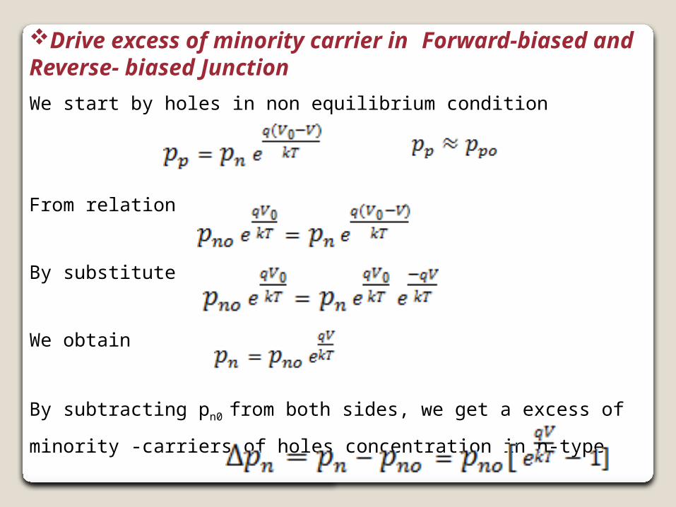
Drive excess of minority carrier in Forward-biased and Reverse- biased Junction
We start by holes in non equilibrium condition
From relation
By substitute
We obtain
By subtracting pn0 from both sides, we get a excess of minority -carriers of holes
concentration in n-type

Drive excess of minority carrier in Forward-biased and Reverse- biased Junction
Similarly, electrons in non equilibrium condition
From relation
By substitute
We obtain
By subtracting np0 from both sides, we get a excess of minority -carriers of
electrons concentration in p-type

Mathematical description of excess of minority carrier in Forward-biased and Reverse- biased Junction
From previous lectures, we discussed about the equation for diffusion of minority
carriers
The solution for it is where A and B are constants
which can be found from boundary conditions (from the following figure a
semiconductor p-type variable concentration in one dimension)
(In the case of bias {non- equilibrium} we will deal of low-level injection)
Therefore, we assume that
And
Therefore, we obtain

Mathematical description of excess of minority carrier in Forward-biased and Reverse- biased Junction
Similar, in case of bias in junction
=

Mathematical description of excess of minority carrier in Forward-biased and Reverse- biased Junction to Drive diffusion current
Similar, in case of bias in junction
Thus, the equation for diffusion of minority carriers in n –type & p- type is
By substituting to excess minority -carriers concentration from previous derivation
In focusing of borders depletion region, we obtain

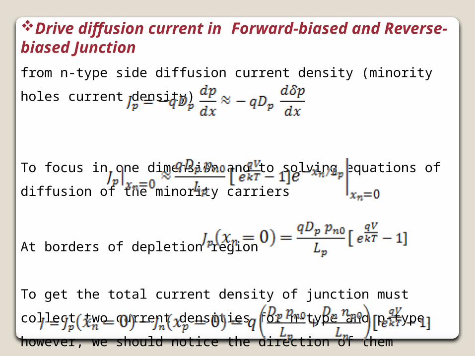
Drive diffusion current in Forward-biased and Reverse- biased Junction
We notice that diffusion current variables in equilibrium condition (or the
absence of bias) while drift current does not change its status in equilibrium
condition .
To get the current density in the junction : first from p-type side (minority
electrons current density)
To focus in one dimension and to solving equations of diffusion of the minority
carriers
At borders of depletion region
=
Drive diffusion current in Forward-biased and Reverse- biased Junction
from n-type side diffusion current density (minority holes current density)
To focus in one dimension and to solving equations of diffusion of the minority
carriers
At borders of depletion region
To get the total current density of junction must collect two current densities for
n-type and p-type, however, we should notice the direction of them

Drive diffusion current in Forward-biased and Reverse- biased Junction
From the figure
To calculate the current
Where the reverse saturation current is

Drive diffusion current in Forward-biased and Reverse- biased Junction
Figure illustrates the distribution of the electron and hole currents in the junction
in the forward bias

I – V Characteristic of Forward-biased and Reverse-biased Junction
You studied at electronic lab the relation between voltage and current of diode in
forward-biased and reverse-biased depending on electrical conductivity to
terminals of battery and diode as in the figure
We conduct first in forward bias then reverse bias.
In addition , a resistor is used to limit the forward current
to a value that will not overheat the diode and cause damage. This resistor called
dynamic resistance.
To calculate resistance value is inverted slope
dI/dV tangent to the curve. The value of
resistance in forward bias less than the value
in reverse bias Rf < Rb

I – V Characteristic of Forward-biased and Reverse-biased Junction
At forward bias circuit, we notice when increasing forward voltage, there is a flow in the
current (diffusion current here). After
the voltage value reaches to (barrier
potential), the forward current increase
rapidly (barrier potential for Si is 0.7v
and Ge is 0.3 v ) . From figure and
explanation, we notice that diode is not
linear which not depend on Ohm’s law
due to first quarter of graph.
=

I – V Characteristic of Forward-biased and Reverse-biased Junction
At reverse bias circuit as fourth quarter of
graph , there is small value of voltage and
constant in relation between reverse voltage
and diffusion current (which called Reverse
Saturation Current). Keeping in mind, reverse
voltage has large value compared with forward
voltage to reached a particular voltage called
Avalanche Voltage. This is shown clearly when
we study a special type of diodes : Zener diode.
The current increase very rapidly after
Zener Breakdown or Breakdown voltage VBR

I – V Characteristic of Forward-biased and Reverse-biased Junction
the relation between diffusion
current and applied voltage
Forward-biased
Reverse-biased
is an exponential relation
Where I0 is reverse saturation current

I – V Characteristic of Forward-biased and Reverse-biased Junction
Temperature Effect : for forward-biased diode as temperature is increased, the
forward current increases for a given value of forward voltage. For a given value
of forward current, the forward voltage decrease,
as shown in figure. The blue curve is at room
temperature and red curve is elevated temperature
(300K + ΔT) notice that barrier potential decreases
as temperature increases. For reverse-biased diode
as temperature is increased, the reverse current
increases. However, there different between two
curves. Keep in mind that the reverse current
breakdown remains extremely small and can usually
be neglected

Diode Models
There are three models for diode
1-The Ideal Model:
This model is a simple switch. When the diode is forward-biased, it acts like a
closed (on) switch. When it is reverse –biased, it acts like a closed (off) switch.
the barrier potential, the forward dynamic resistance, and the reverse current are
all neglected in this model.

Diode Models2- The practical Model
The practical model adds the barrier potential to ideal model. When the diode is
forward-biased, it is equivalent to a closed switch in series with a small
equivalent voltage source equal to the barrier potential. When the diode is
reverse-biased , it is equivalent to an open switch just as ideal model because
barrier potential does not affect reverse bias.

Diode Models
3- The Complete Model:
This model consists of the barrier potential, the small forward dynamic
resistance, and the large internal reverse resistance.

Pn Junction’s mission
Of the most important uses and benefits of the pn junction is the rectifier
current from alternating current to direct current and you will study in detail that
in Electronics Lab. where junction connect to AC source (which current shape
wave or sine with time) to take advantage of the forward bias (passing current)
reverse bias (not passage current) are rectifier the alternating current.
There are two types of rectifier: half – wave rectifier and full wave rectifier.
In addition to rectifier process, the filter process came next. By putting
capacitor that will improve the current form of half wave or full wave into a form
close to a straight line by putting a number of capacitors
After rectifier and filter processes, regulator process came third (which we can
put Zener diode) that give straight current.
Three processes (rectifier , filter , regulator) to transformation from alternating
current to direct current

Half-Wave Rectifiers =

Half-Wave Rectifiers
To calculate average value of half-wave rectified output voltage
However, this calculation for ideal diode. So in practical diode, we take in the
account the barrier potential
AVAVG
Vp
0T
BRinPoutP VVV )()(
+
-
+
RL0
0.7 V
Vp(in)-
V
0
=V p(in)p(out) - 0.7V
P
AVGV
VPeriod
Area
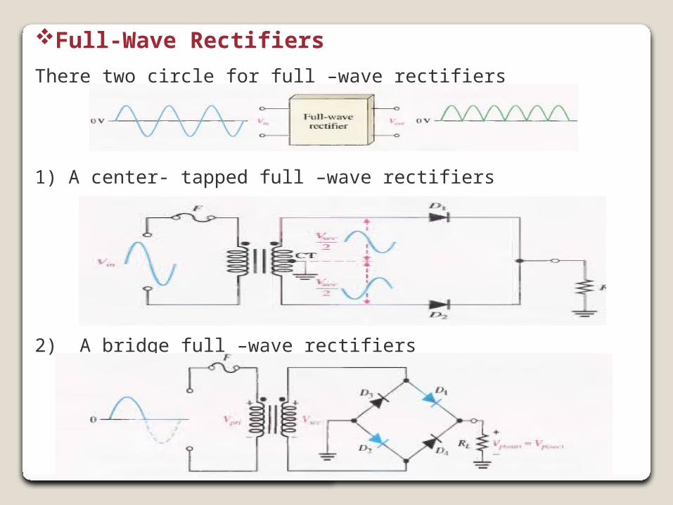
Full-Wave Rectifiers
There two circle for full –wave rectifiers
1) A center- tapped full –wave rectifiers
2) A bridge full –wave rectifiers

center- tapped Full-Wave Rectifiers =

The Bridge Full-Wave Rectifiers =

Filters
By using capacitor
half or fall – wave is
filtered. By putting
number of capacitors,
the wave is filtered
more than before

Regulator
The final step to transformation from alternating current to direct current is
regulator. There are numbers of regulator devices. One of them is Zener diode

Zener diodeZener diode differs from normal pn junction in its designed to work in reverse breakdown area without the occurrence of any problems. Difference in Zener diode differential has more impurities in one of side of diode than the other as (n+p ) or ( p+n). In equilibrium condition Fermi level at the same energy level in n-type and p-type, but in non equilibrium condition opposite as we knew. However, in the case of reverse bias aligns the conduction band in the n-type and valence band in the p-type as if they are at the same energy level and thus the electron from the conduction band in the n-type moves (or tunneling) to the valence band in p-type as shown in the figure. Among the benefits of this diode is used in regulate voltage.
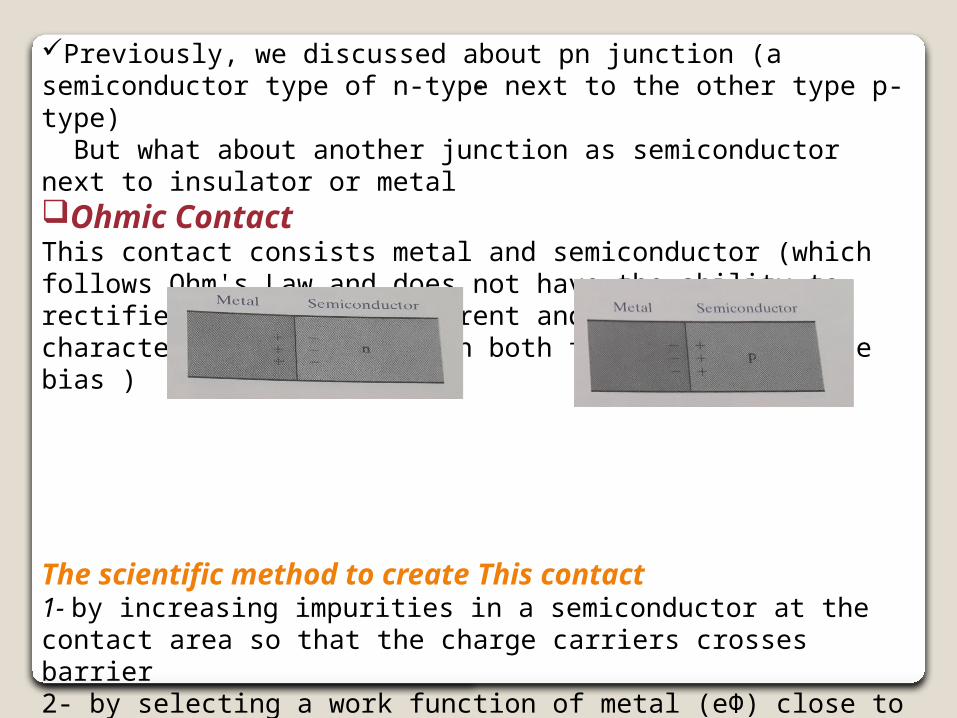
Previously, we discussed about pn junction (a semiconductor type of n-type next to the other type p-type) But what about another junction as semiconductor next to insulator or metalOhmic ContactThis contact consists metal and semiconductor (which follows Ohm's Law and does not have the ability to rectifier current and (current and voltage) characteristic is linear in both forward and reverse bias )
The scientific method to create This contact1- by increasing impurities in a semiconductor at the contact area so that the charge carriers crosses barrier2- by selecting a work function of metal (eΦ) close to work function of semiconductorwork function: the required energy to remove an electron from Fermi level or required energy for ionization metal
=

Ohmic Contact
The left figure illustrates Fermi level and work function in the metal and
semiconductor (n-type) before contact. The right figure illustrates them when
configure junction of metal and semiconductor (n-type) in equilibrium condition
and how Fermi level aligning between metal and semiconductor (when there are
negative charges close to surface of metal, they attract positive charges in metal )
=

Ohmic Contact
The left figure illustrates Fermi level and work function in the metal and
semiconductor (p-type) before contact. The right figure illustrates them when
configure junction of metal and semiconductor (p-type) in equilibrium condition
and how Fermi level aligning between metal and semiconductor (when there are
positive charges close to surface of metal, they attract negative charges in metal )
=

Metal–Oxide–Semiconductor Contact (MOS)
structure
In this contact, a thin layer of oxide is put on the surface of a semiconductor n-
type or p-type. Then, pole metallic (metal) is put above the surface of the oxide
layer . We should choose a good electrical insulation of oxide which has a large
energy gap and isolates the metal from the semiconductor which no passing
electrical current between them.
In thermal equilibrium condition
In the absence of application of the electric
field or the voltage, the Fermi and connection
and valence levels are horizontal and flat.
When applying an electric field, there is
a bending in energy levels

Metal–Oxide–Semiconductor Contact (MOS)
Effect of voltage bias
According to the applied voltage on this contact, it will consist three different
situations such as what is shown in figure .
1- depletion 2- inversion 3- accumulation
=

Metal–Oxide–Semiconductor Contact (MOS)
Effect of voltage bias (metal and n-type contact)
1 - Depletion :
When applying negative bias voltage at the surface of metal, a small amount of
negative charges is made. Then, the oxide layer prevent electric current from
passage to semiconductor . However, the electrons in substrate of semiconductor
n-type will be affected by these negative charges and moved away from the area
located under oxide and created the depletion region in semiconductor similar to
those that created in pn Junction
=

Metal–Oxide–Semiconductor Contact (MOS)
Effect of voltage bias (metal and n-type contact)
2 - Inversion
When increasing a negative bias voltage on surface of metal, Instead of
expanding more of depletion region within the semiconductor, inversion status is
formed which holes gather next to the surface of the oxide. Those holes is the
minority carriers in the semiconductor n-type.
3 - Accumulation
When applying positive bias voltage at the surface of metal, negative majority
carriers attract and accumulate at the surface of the oxide in semiconductor n-
type.
=

Metal–Oxide–Semiconductor Contact (MOS)
Energy levels forms in MOS in different bias (metal and p-type contact)
1- Depletion :
When applying positive bias voltage, Fermi level move down from its first
location in thermal equilibrium condition. Also,
straight bend at the energy level in oxide
and energy levels of the semiconductor p-type
move down near the interface of oxide.
In addition, electrons drop down in potential
well. We notice that the distribution of carriers
density of per unit area in semiconductor p-type
equal in the metal
=

Metal–Oxide–Semiconductor Contact (MOS)
Energy levels forms in MOS in different bias (metal and p-type contact) 2 - Inversion When increasing positive bias voltage more than threshold voltage VT ; the semiconductor inverse and electrons occupyinversion layer. Fermi level move more down from its first location in thermal equilibrium condition. Also, straight bend at the energylevel in oxide and energy levels of semiconductor p-type move more down near interface of oxide. In addition, electrons dropmore down in potential well. We notice that thedistribution of carriers density of per unit area in semiconductor p-type for maximum depletion region Wmax in addition to carrier of inversion layer Qn equal in the metal
=

Metal–Oxide–Semiconductor Contact (MOS)
Energy levels forms in MOS in different bias (metal and p-type contact)
3- Accumulation
When applying negative bias voltage, Fermi level move up from its first location
in thermal equilibrium condition. Also,
straight bend at the energy level in oxide
and energy levels of the semiconductor p-type
move up near the interface of oxide.
In addition, holes climb up in potential
well. We notice that the distribution of carriers
density of per unit area in semiconductor p-type
equal in the metal
=

Recommended