EEL6935 Advanced MEMS 2005 H. Xie 1
Lecture 13Agenda:
RF MEMS: Introduction
3/7/2005
EEL6935 Advanced MEMS (Spring 2005) Instructor: Dr. Huikai Xie
EEL6935 Advanced MEMS 2005 H. Xie 2
Wireless Communications
4G3G2G1G
>2Mb/s to moving vehicles
~384kb/s to moving vehicles
Macro/micro/picocell
Macro cell
GPS (globe positioning system), “messages in space”
Higher speed, improved voice/multimedia mobility, internet
Voice + dataVoice
UMTS (Universal Mobile Telecommunications System)
GSM (Global System for Mobile Communication)
900 MHz
Multistandard + multiband
Multimode, multiband
Digital (dual-mode, dual-band)
Analog (single-band)
EEL6935 Advanced MEMS 2005 H. Xie 3
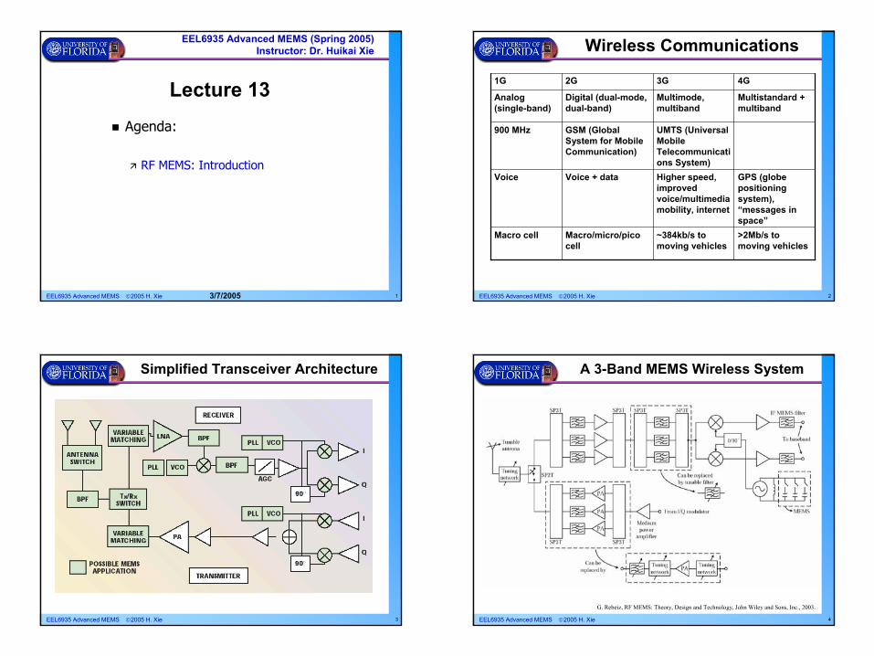
Simplified Transceiver Architecture
EEL6935 Advanced MEMS 2005 H. Xie 4
A 3-Band MEMS Wireless System
G. Rebeiz, RF MEMS: Theory, Design and Technology, John Wiley and Sons, Inc., 2003.

EEL6935 Advanced MEMS 2005 H. Xie 5
MEMS-Based Wireless Applications
High-Q Passives• Inductors
• Varactors
• Transmission lines
• Switches
• Resonators
Circuits/Systems• Oscillators
• Mixers
• Power amplifiers
• Phase shifters
• Filters
• Switch matrices
• Transceivers
EEL6935 Advanced MEMS 2005 H. Xie 6
RF MEMS Application Areas
RF MEMS Switches and Varactors• Low loss and low power consumption (0.1 dB up to 120 GHz)• High Isolation (> 30 dB up to 100 GHz)• Potential for low cost fabrication (no epi layers, no 0.15 um litho.)• Very high Q possible with varactors (and large capacitance range)• Very low intermodulation products (> 60 dBm)
RF MEMS Inductors• Very high Q possible (Q > 50 at 1-5 GHz)• Built using MEMS processes but nothing moves (not tunable)
RF MEMS Filters• Very small size possible (1000x reduction in size in element)• Extremely high-Q (5,000 to 50,000)• Compatible with CMOS and potential for low cost
EEL6935 Advanced MEMS 2005 H. Xie 7
Comparison of Different Switches
Isol
atio
n (d
B)
Insertion Loss (dB)
MEMS: MEMS switchesPIN: GaAs P-I-N DiodesFET: GaAs Transistors
MEMS switches•Good isolation•Low insertion loss
G. Rebeiz, RF MEMS: Theory, Design and Technology, John Wiley and Sons, Inc., 2003.
EEL6935 Advanced MEMS 2005 H. Xie 8
Example RF MEMS Devices
Capacitive Switch (Lincoln Lab)
Pull-down
Metal-contact Switch (Analog Devices)
MEMS Oscillator (U-Michigan)MEMS Inductor (KAIST)
EEL6935 Advanced MEMS 2005 H. Xie 9
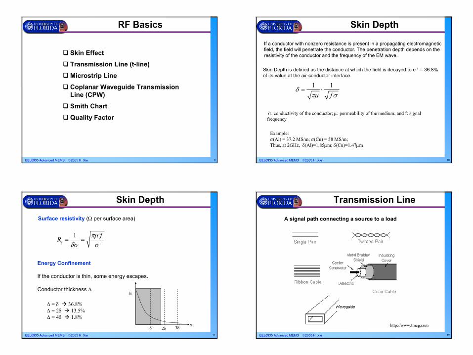
RF Basics
Skin Effect
Transmission Line (t-line)
Microstrip Line
Coplanar Waveguide Transmission Line (CPW)
Smith Chart
Quality Factor
EEL6935 Advanced MEMS 2005 H. Xie 10
Skin Depth
If a conductor with nonzero resistance is present in a propagating electromagnetic field, the field will penetrate the conductor. The penetration depth depends on the resistivity of the conductor and the frequency of the EM wave.
Skin Depth is defined as the distance at which the field is decayed to e-1 = 36.8% of its value at the air-conductor interface.
1 1f
δπµ σ
= ⋅
σ: conductivity of the conductor; µ: permeability of the medium; and f: signal frequency
Example:σ(Al) = 37.2 MS/m; σ(Cu) = 58 MS/m; Thus, at 2GHz, δ(Al)=1.85µm; δ(Cu)=1.47µm
EEL6935 Advanced MEMS 2005 H. Xie 11
Skin Depth
Surface resistivity (Ω per surface area)
1s
fR πµδσ σ
= =
Energy Confinement
If the conductor is thin, some energy escapes.
Conductor thickness ∆
∆ = δ 36.8%∆ = 2δ 13.5%∆ = 4δ 1.8%
δ 2δ 3δ
E
x
EEL6935 Advanced MEMS 2005 H. Xie 12
Transmission Line
http://www.tmeg.com
A signal path connecting a source to a load

EEL6935 Advanced MEMS 2005 H. Xie 13
Transmission Line
http://www.tmeg.com
Characteristic Impedance
Circuit Model
0forward
forward
VZ
I=
EEL6935 Advanced MEMS 2005 H. Xie 14
Transmission Line
http://www.tmeg.com
Characteristic Impedance
Free space 00
0
120Zµ
πε
= = Ω
Low-resistive lines0 /Z L C=
Parallel Wires
0276 2log
r
DZdε
=
Coaxial Cable
0138 log
r
DZdε
=
EEL6935 Advanced MEMS 2005 H. Xie 15
Transmission Line
http://www.tmeg.com
Reflection Coefficient
0
0
reflected load
forward load
V Z ZV Z Z
−Γ = =
+
• Impedance matching is needed to reduce reflection power.
• When the load impedance is greater than the transmission line impedance, a power reflection occurs but no phase shift.
• When the load impedance is smaller than the transmission line impedance, a power reflection also occurs with 180°phase shift.
EEL6935 Advanced MEMS 2005 H. Xie 16
Smith ChartReflection Coefficient
0
0
reflected load
forward load
V Z ZV Z Z
−Γ = =
+
0 0
0 0
1 11 1
L L L
L L L
Z Z Z Z zZ Z Z Z z
− − −Γ = =
+ + +
11Lz
+ Γ=
− Γ
11
r iL L
r i
jr jxj
+ Γ + Γ+ =
− Γ − Γresistance reactance
Real partImaginary part
rΓ
iΓ

EEL6935 Advanced MEMS 2005 H. Xie 17
Smith ChartReal part (resistance)
( )
2 2
2 2
11
r iL
r i
r − Γ − Γ=
− Γ + Γ
Imaginary part (reactance)
( )2 2
21
iL
r i
x Γ=
− Γ + Γ
2 2
2 11 1
Lr i
L L
rr r
Γ − + Γ = + +
( )2 2
2 1 11r iL Lx x
Γ − + Γ − =
rΓ
iΓ iΓ
rΓ
Lx
rL
Both imaginary and real parts can be expressed on the same chart EEL6935 Advanced MEMS 2005 H. Xie 18
Smith Chart
The coexistence of complex-impedance and complex-reflection-coefficient information on a single graph allows you to easily determine how values of one affect the other. You can find what complex reflection coefficient would result from connecting a particular load impedance to a system having a given characteristic impedance.
Overlay the two circle clusters on a single 2D plot, resulting in a SMITH CHART.
0iΓ =
rL
xL
0rΓ =
EEL6935 Advanced MEMS 2005 H. Xie 19
Smith Chart
Example:
Rick Nelson, Test & Measurement World, July 2001http://www.web-ee.com/primers/files/SmithCharts/smith_charts.htm
1 2Z j= +
0.5 0.50.707 / 45
jΓ = += °
EEL6935 Advanced MEMS 2005 H. Xie 20
Microstrip Line
Conventional Microstrip
Dielectric layer(hundreds microns thick)
w w
Thin-film microstrip lines (TFMSL) are miniaturized microstrip lines (a signal conductor, a dielectric and a ground conductor), located on top of the silicon substrate. The ground metallization shields the line from the silicon substrate effects; therefore low resistivity silicon substrates can be used without deteriorating microwave performance.
Thin-Film Microstrip
Si substrate
Dielectric layer (e.g., BCB)
Small dimensions increase conductor loss. Finite metal conductivity and internal inductance must be taken into account.

EEL6935 Advanced MEMS 2005 H. Xie 21
Thin-Film Microstrip Line
Equivalent Circuit Modelw
tht
εrR L
C GL: Inductance per unit lengthC: capacitance per unit lengthR: resistance per unit length G: conductance per unit length
• co: free-space light velocity; εr,eff: effective relative dielectric constant• ZLO: characteristic impedance for lossless case with t=0 • weq,0: equivalent signal conductor width without dielectric substrate, which
takes into account the finite thickness of the signal line• G accounts for the dielectric loss of the substrate, described by the dielectric
loss tangent, tan(δε).
,
0 0 0( )r eff
L eq
Cc Z w
ε=
⋅( ),
0 0 0
1tan
1 ( )r eff r
r L eq
G wc Z w ε
ε εδ
ε−
= ⋅ ⋅ ⋅− ⋅
EEL6935 Advanced MEMS 2005 H. Xie 22
Coplanar Waveguide
• Ease of parallel and series insertion of both active and passive components• High circuit density• The traces of CPW transmission lines can be changed to match component
lead widths while keeping the characteristic impedance constant
S w S
EEL6935 Advanced MEMS 2005 H. Xie 23
Coplanar Waveguide
, 0( ( ), , )r effw S S H Zξ ε= ⋅
T. Deng, “CAD Model for Coplanar Waveguide Synthesis,” IEEE Transactions On Microwave Theory And Techniques, Vol. 44, No. 10, October 1996
S w S
Hεr
• CPW Trace Width Synthesis
, 0( ( ), , )r effS w w H Zξ ε= ⋅
( ), , 0( , , , )r eff r eff rS H Z Sε ε ε=
( ), , 0( , , , )r eff r eff rS H Z Sε ε ε=
where
CPW Design
• CPW Trace Spacing Synthesis
where
EEL6935 Advanced MEMS 2005 H. Xie 24
Coplanar Waveguide
T. Deng, “CAD Model for Coplanar Waveguide Synthesis,” IEEE Transactions On Microwave Theory And Techniques, Vol. 44, No. 10, October 1996
( )
( )
0 0
0 0, ,
00
, 0 1
0,
0
00
1 exp exp 14 4 4
2 1( , )
1 exp 2 18
2 1
r eff r eff
rr eff
r eff
r
Z Z
for Z
Z
Z
for Z
η ηπ πε ε
η
εξ ε
ηπ ε
η
ε
−
+ − −
<+
=
− ≥ +
where the free-space impedance 0 377η = Ω

EEL6935 Advanced MEMS 2005 H. Xie 25
Quality Factor
De Los Santos, RF MEMS Circuit Design, Artech House, 2002
maximum instantaneous energy stored2energy dissipated per cycle
Q π= ×
Resonant Circuits,
0 resonant frequencybandwidth
fQB
= =
0capacitor
CQG
ω=
Capacitor with a shunt parasitic conductance G
Inductor with a series parasitic resistance R
0inductor
LQ
Rω
=
Presence of an external load RL
1 1 1
Ltotal unloaded RQ Q Q= +
0
0L
LR
L
L RQ orR L
ωω
=
series parallel
EEL6935 Advanced MEMS 2005 H. Xie 26
References
G. Rebeiz, RF MEMS: Theory, Design and Technology, John Wiley and Sons, Inc., 2003.
De Los Santos, RF MEMS Circuit Design, Artech House, 2002.
Rick Nelson, How does a Smith chart work?, Test & Measurement World, July 2001. Also available at http://privatewww.essex.ac.uk/~mpthak/smith_charts.htm
Transmission lines, http://www.tmeg.com
Recommended