DLTS analysis of amphoteric interface defects in high-k
TiO2 MOS structures prepared by sol-gel spin-coating
Arvind kumar
Dept. of Physics
IISc, Bangalore
11/28/2015 1

11/28/2015 2
Outline
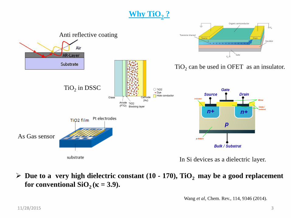
Why TiO2 ?
The deposition of high- TiO2 films by solution route.
Material characterization and films morphology.
Fabrication of MOS structure.
Interface states density (Dit) analysis by DLTS.
Capture cross – section analysis by IF – DLTS.
Summary
11/28/2015 3
TiO2 can be used in OFET as an insulator.
TiO2 in DSSC
In Si devices as a dielectric layer.
Anti reflective coating
As Gas sensor
Due to a very high dielectric constant (10 - 170), TiO2 may be a good replacement
for conventional SiO2 ( = 3.9).
Why TiO2 ?
Wang et al, Chem. Rev., 114, 9346 (2014).
11/28/2015 4
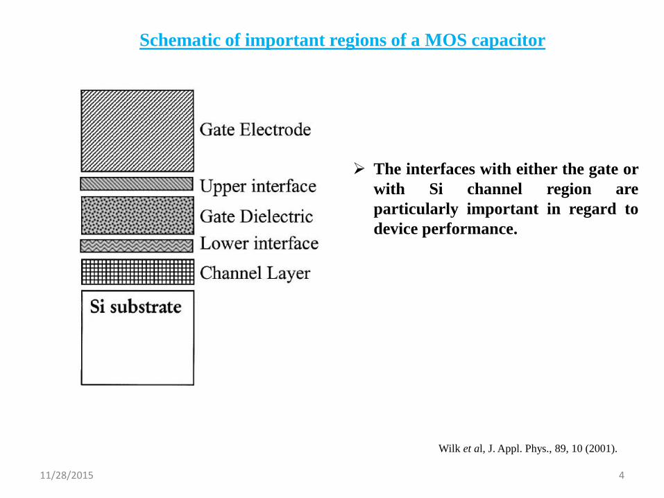
Schematic of important regions of a MOS capacitor
The interfaces with either the gate or
with Si channel region are
particularly important in regard to
device performance.
Wilk et al, J. Appl. Phys., 89, 10 (2001).

888 Isopropyl alcohol (IPA) 8.5 ml
Titanium isopropoxide (TIP) 0.6 ml
Hydrochloric acid (HCl) 20 µL
Ageing for 12 Hour
A transparent solution was obtained
This can be used for spin coating
11/28/2015 5
Preparation of solution
Arvind et al, Mater. Sci .Semi. Proc. 40, 77 (2015).

11/28/2015 6
p –Si (100)
TiO2 film
The deposition of high- TiO2 thin films by solution route:

11/28/2015 7
XRD analysis
XRD analysis suggests a well-crystallized
anatase phase of nc-TiO2 films on Si.
XRD of 600 0C annealed TiO2 film on Silicon.
Arvind et al, Mater. Sci .Semi. Proc. 40, 77 (2015).

11/28/2015 8
Raman spectrum of 600 0C annealed TiO2 film
on Si and Quartz substrate.
Raman spectrum confirms the presence of
well-crystallized anatase phase of
titanium dioxide film on quartz and Si.
Raman spectrum
The results are in close agreement with
XRD analysis.
Arvind et al, Mater. Sci .Semi. Proc. 40, 77 (2015).

XPS survey scan spectra
Ti2p core level spectra
The separation between the Ti 2p3/2 and the
Ti 2p1/2 peaks is 5.79 eV, which the presence
of Ti in its tetravalent state.
O1s core level spectra Arvind et al, Mater. Sci .Semi. Proc. 40, 77 (2015).
11/28/2015 10
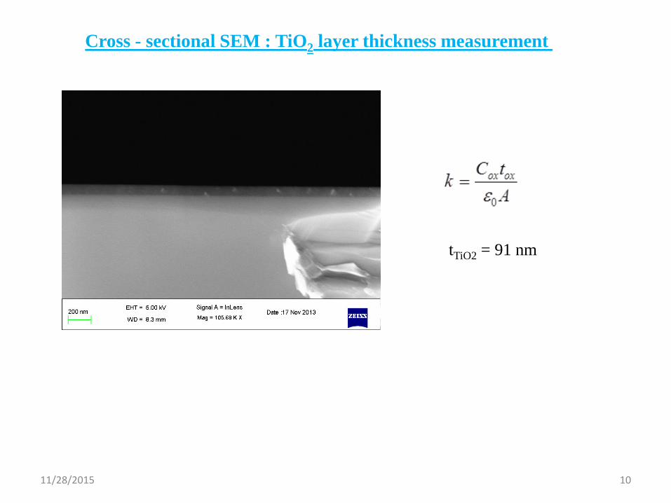
Cross - sectional SEM : TiO2 layer thickness measurement
tTiO2 = 91 nm

400 500 600 700 800 900
2.3
2.4
2.5
2.6
Refr
acti
ve in
dex (
n)
wavelenght (nm)400 500 600 700 800 900 1000
14
16
18
20
22
24
26
28
30
32
(Experimental)
(fitted)
(Experimental)
(Fitted)
Wavelength (nm)
(
deg)
40
60
80
100
120
140
(
de
g)
2
2
11
1d
nPorosity
n
Ellipsometry Studies
The porosity is 10 %.
Arvind et al, Mater. Sci .Semi. Proc. 40, 77 (2015).

11/28/2015 12
The RMS surface roughness is 6 Å.
Roughness analysis
Arvind et al, Mater. Sci .Semi. Proc. 40, 77 (2015).

11/28/2015 13
p –Si (100)
Electrical measurement
MOS capacitor fabrication and measurement
A metal mask having circular hole (d = 288 µ) was used to deposit the Al on
top of TiO2 films. Thermal evaporation technique was used for Al deposition
and thickness was 200 nm.

p-Si (100) T05 header
Device mounted on T05 header for DLTS measurements.
11/28/2015 14
Schematic diagram of Al/TiO2/p-Si(100) MOS Device.
Estimation of Interface states density (Dit) by DLTS

Voltage-time (V-t) and capacitance time (C-t)
diagrams. VQ is the quiescent voltage and VP is
the majority carrier pulse voltage.
Energy band diagrams of Al/TiO2/p-Si(100) MOS devices
(a) Before (b) on, and (c) after majority carrier pulse. Kundu et al, J. Vac. Sci. Tech B 30, 051206 (2012).
DLTS Theory
11/28/2015 15
( )exp T V
p p th v
E Ee V N
kT

16
Arrhenius plot obtained from the
peak positions
51000 8.617 10TE slope
Khan et al., Conf. Rec. of the 2006 IEEE 4th World Conf. on (Vol. 2, pp. 1763-1768). IEEE.

DLTS Setup in our lab
17

C-V characteristic of Al/TiO2/Si (100) MOS
11/28/2015 18
ox FBot
C VQ
q
2high SiO
high
tEOT
The flat – band voltage (VFB) and the density of oxide trapped charges
estimated are – 0.9, – 0.44 V and 5.24×10¹⁰, 1.03×1011 cm−2; for the NMOS
and PMOS capacitors, respectively.
EOT was estimated 4.5 nm.
Arvind et al, AIP Advances 5, 117122 (2015).
C-V analysis

DLTS spectra at different rate windows (tw) on N and PMOS.
11/28/2015 19
The filling pulse is applied from
accumulation to depletion region.
Filling pulse width was taken 5 ms for all
rate windows.
DLTS measurements
51000 8.617 10TE slope
The activation energy of the trap (ET)
is estimated to be 0.30 eV for p-Si
substrate and 0.21eV for n-Si
substrate.
Arvind et al, AIP Advances 5, 117122 (2015).

11/28/2015 20
Interface analysis
3
0 2 1ln( / )
si ox Ait
C N CD
C kT t t
The interface states (Dit) were estimated 8.73×10¹¹ and 6.41×10¹¹ eV−1 cm−2
for NMOS and PMOS, respectively.
This is an order of magnitude higher than Al/SiO2/Si MOS devices.
Still this is an acceptable value for Si/high-k (non – native Oxide) MOS
devices and consistent with other deposition techniques.
175 200 225 250 275
-160
-140
-120
-100
-80
-60
-40
-20
0
DL
TS
Sig
na
l (f
F)
Temperature (K)
1 us
2 us
4 us
10 us
20 us
40 us
100 us
200 us
400 us
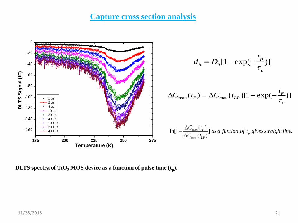
DLTS spectra of TiO2 MOS device as a function of pulse time (tp).
11/28/2015 21
Capture cross section analysis
[1 exp( )]Pit it
c
td D
max max( ) ( )[1 exp( )]PP LP
c
tC t C t
max
max
( )ln[1 ] .
( )
Pp
LP
C tas a funtion of t gives straight line
C t

DLTS spectra of TiO2 MOS device as a function of pulse time (tp).
11/28/2015 22
Capture cross section analysis
1p
c thV p
The capture cross – sections estimated
is 5.8×10⁻²³, 8.11×10⁻²³ cm2 for
NMOS and PMOS interface traps.
Arvind et al, AIP Advances 5, 117122 (2015).
Summary
High quality TiO2 thin films have been deposited by combined sol – gel spin – coating
method.
The small surface roughness of 6 Å is achieved.
Reasonably low (Dit) are 8.73×10¹¹ and 6.41×10¹¹ eV−1 cm−2 achieved for NMOS and
PMOS, respectively.
Very low capture cross section indicates that the traps are not aggressive recombination
centers and possibly can not contribute to the device operation to a large extent.
This method might be a good replacement for the expensive high vacuum deposition
techniques in the development of new high-κ dielectrics.
DLTS study provide a better understanding of TiO2/Si interfaces.
11/28/2015 23

11/28/2015 24
[1] D V Lang, J. Appl. Phys., vol. 45 (1974) 3023.
[2] K Yamasaki et al, Jpn. J. Appl. Phys. 18, 113 (1979).
[3] S Kundu et al, Journal of Vacuum Science Technology B 30,051206 (2012).
[4] E Simoen, ECS Transactions, 41 (4) 37-44 (2011).
[5] S Jeon, Appl. Phys. Letters, vol. 82 (2003) 7.
[6] Hua Min Li et al, Thin Solid Films 518(2010) 6382-6384.
[7] A. Kumar, S. Mondal, and K.S.R.K. Rao, AIP Conf. Proc. 1665, 080015 (2015).
[8] A. Kumar, S. Mondal, S.G. Kumar, and K.S.R. Koteswara Rao, Mater. Sci .Semi. Proc. 40, 77 (2015).
[9] A. Kumar, S. Mondal, and K.S.R.K. Rao, AIP Advances 5, 117122 (2015).
References:
11/28/2015 25
This work has been done in collaboration with Sandip Mondal.
UGC-CSIR for research scholarship.
We acknowledges the financial support from STC- ISRO.
We thank CeNSE, IISc, for providing various characterization facility.
Acknowledgements

11/28/2015 26
Recommended