International Research Journal of Engineering and Technology (IRJET) e-ISSN: 2395-0056
Volume: 02 Issue: 08 | Nov-2015 www.irjet.net p-ISSN: 2395-0072
© 2015, IRJET ISO 9001:2008 Certified Journal Page 337
DESIGN OF DIGITAL CIRCUITS USING REVERSIBLE LOGIC AT 32nm
TECHNOLOGY
M. Madhuri1 Mr. R. Niranjan2
1 M.Tech student, Dept. of ECE, VLSI System Design, JNTUA, Ananthapuramu, Andhra Pradesh, India. 2Member of Technical Staff, SEER Academy, Hyderabad, India. ---------------------------------------------------------------------***---------------------------------------------------------------------
Abstract - Reversible logic has presented itself as a prominent technology which plays an imperative role in Quantum Computing. Quantum computing devices theoretically operate at ultra high speed and consume less power. Research done in this paper aims to utilize the idea of reversible logic to break the conventional speed-power trade-off, there by getting a step closer to realize Quantum computing devices. To authenticate this research, various Digital circuits are implemented such as a 4-bit Ripple-carry Adder, 8-bit Wallace Tree Multiplier, and 16bit GCD unit are implemented using Reversible Logic. The power and area parameters for the circuits have been indicated, and compared with the 32nm and 90 nm Technologies. The comparative statistical study proves that circuits employing 32nm technology Reversible Digital Circuits are area and power efficient. The designs presented in this paper were simulated using VCS-Synopsys.
Key Words: Reversible logic. Quantum Computing, high speed, Low Power, Area efficient, Trade off,ripple carry adder,8-bit Wallace Tree multiplier,16-bit GCD Unit,32nm Technology,90nm Technology.
1. INTRODUCTION Reversible logic gates are widely used in low power VLSI.Reversible gates have the capability of back-computation and reduced power dissipation, as there is no loss of information [1]. Basic reversible gates are employed to achieve the required functionality of a reversible circuit. The uniqueness of reversible logic is that, there is no loss of information as there is one-to-one correspondence Between the inputs and outputs. This enables the system to run backwards and while doing so, any intermediate design stage can be thoroughly examined. The fan-out of each block in the circuit has to be one.
This research paper focuses on implementation of reversible Digital circuits at 32nm technology in which main aim is to optimize the area and power of the design. Digital Circuits are designed using basic reversible gates. in this paper 4-bit full adder, 8-bit reversible Wallace tree
multiplier are devised and then compared with the 32nm and 90nm technologies in terms of speed, power. sequential circuits are the heart of digital designing, the design for the reversible 16 bit GCD unit has been proposed using Reversible logic gates. As a results 32nm technology designings are area and power efficient so these digital circuits are implemented in 32nm technology.
II. REVERSIBLE LOGIC Boolean logic is said to be reversible if the set of inputs Mapped have an equal number of outputs mapped i.e. they have one-to-one correspondence. This is realized employing reversible gates in the designs. Any circuit having only reversible gates is capable of dissipating no power [2].
Goals of Reversible Logic: A. Quantum Cost: Quantum cost of a circuit is the measure of implementation cost of quantum circuits. More precisely, quantum cost is defined as the number of elementary quantum operations needed to realize a gate. B. Speed of Computation: The time delay of the circuits should be as low as possible as there are numerous computations that have to be done in a system involving a quantum processor; hence speed of computation is a very important parameter while examining such systems. C. Garbage Outputs: Garbage outputs are those output signals which do not contribute in driving further blocks in the design. These outputs become redundant as they are not required for computation at a later stage. The garbage outputs make the system slower; hence for better efficiency it is necessary to minimize the number of garbage outputs. D. Feedback: when designing Reversible circuits looping is prohibited E. Fan-out: The output of a certain block in the design can only drive at most one block in the design. Hence it can be said that the Fan-out is restricted to 1.
III. REVERSIBLE GATES There are many reversible gates such as Feynman, Toffoli, TSG, Fredkin, Peres, etc [3]. As the universal gates in

International Research Journal of Engineering and Technology (IRJET) e-ISSN: 2395-0056
Volume: 02 Issue: 08 | Nov-2015 www.irjet.net p-ISSN: 2395-0072
© 2015, IRJET ISO 9001:2008 Certified Journal Page 338
Boolean logic are Nand and Nor, for reversible logic, the universal gates are Feynman and Toffoli gates.
1. Feynman Gate: Feynman gate is a universal gate which is used for signal copying purposes or to obtain the complement of the input signal. The block diagram of Feynman gate is shown in fig.1:
Fig. 1: Feynman Gate
2. Fredkin Gate: It is a basic reversible 3- bit gate used for swapping last two bits depending on the control bit. The control bit here is A, depending on the value of A, bits B and C are selected at outputs Q and R.When A=0, (Q=B, R=C) whereas when A=1, (Q=C,R=B). Its block diagram is as shown in fig. 2:
Fig. 2: Fredkin Gate
3. Peres Gate: It is a basic reversible gate which has 3-Inputs and 3-outputs having inputs (A, B, C) and the Mapped outputs (P=A, Q=A^B, R =(A.B)^C). The block diagram is as shown in fig. 3:
Fig. 3: Peres Gate
4. Toffoli Gate: Toffoli gate is a universal reversible Gate which has three inputs (A, B, C) mapped to three Outputs (P=A, Q=B, R= (A.B)^C). The block diagram Of Toffoli gate is shown in fig. 4:
Fig. 4: Toffoli Gate
5. TSG Gate: TSG gate is a reversible gate which has Four inputs (A, B, C, D) mapped to four outputs (P=A, Q=A^B, R=A^B^D, S=(A^B)^D^AB^C). The block
Diagram of TSG Gate is shown in fig. 5:
Fig. 5: TSG Gate
IV. REVERSIBLE RIPPLE CARRY ADDER The gate used in implementing a reversible ripple-carry Full adder is the TSG gate [4]. The TSG gate functions likea full adder. A reversible ripple-carry adder is faster than the non-reversible adder, since the computation of carry in a reversible adder does not require the computation of Previous stages carry (as indicated in the critical paths).When previous stage carry is being forwarded in the Reversible adder, the computation of previous stage carry and computation regarding sum is done simultaneously whereas in an irreversible adder the next stage carry cannot start any computation till previous stage carry is fully generated. The schematic view for reversible ripple carry adder as shown in fig.6
Fig 6: Schematic view for reversible ripple carry adder
V. WALLACE TREE MULTIPLIER A Wallace tree is an efficient hardwired implementation of a digital circuit that multiplies two integers [5]. The Wallace tree has three steps: 1. Every bit of the multiplicand is multiplied (i.e. AND) by every bit of multiplier, thus yielding n2 results (for n X n multiplication). Depending on position of the multiplied bits, the wires carry different weights, i.e. weight of bit carrying result of a5b6 is 65. 2. The number of partial products is reduced to 2 by layers of full and half adders. 3. The wires are grouped in two numbers, and added using a conventional adder. The circuit diagram of Wallace tree multiplier using reversible gates is shown in fig. 7
International Research Journal of Engineering and Technology (IRJET) e-ISSN: 2395-0056
Volume: 02 Issue: 08 | Nov-2015 www.irjet.net p-ISSN: 2395-0072
© 2015, IRJET ISO 9001:2008 Certified Journal Page 339
Fig 7:block diagram for reversible Wallace tree mutiplier
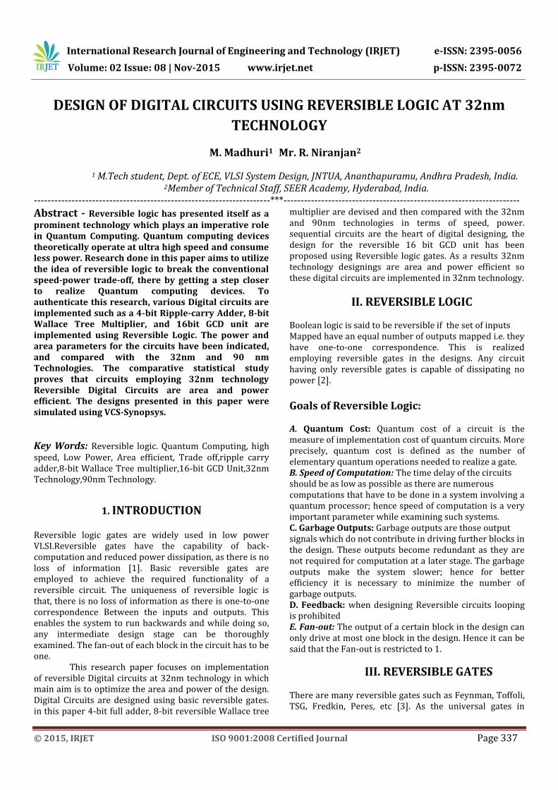
VI. DESIGN OF REVERSIBLE GCD UNIT To illustrate the classical and reversible approaches to the Sequential Control Unit Design, reversible logic is employed for a special purpose processor that computes the GCD of two numbers. This GCD processor incorporates standard Euclid’s Algorithm involving Subtract-Compare-Swap operation of two numbers. The basic principle is to subtract smaller of the two numbers repeatedly from the other number until we get the number that divides another [6].following fig shows the schematic view for GCD processor.
Fig 8: schematic view for GCD processor.
Control Unit Control unit of GCD processor generates the control signals to manipulate the operations in Data-path.
Flip-flop Module: The control unit for GCD processor requires two Flip-flops as binary state encoding is used for FSM. In this Design reversible edge-triggered D Flip-flop is employed for state transitions [7]. Two D-latches are connected in Master-Slave mode to act as an edge-triggered D Flip-flop. Reversible D-latch is designed using Feynman and Fredkin gates [8].
Regeneration Module To avoid multiple fan-out condition in the design, it is necessary to duplicate signals used for computation of output and next state. The duplication of input signals is achieved using Feynman gates.
Output Module The computation of the outputs and Next-state signals is done using reversible Fredkin gates. The functioning of output signals is driven by the algorithm.
VII RESULTS
Simulation results for digital circuits
Implemented the digital circuits like 4-bit
Reversible Ripple Carry Adder ,8-bit Reversible Wallace
tree Multiplier and Reversible 16 bit GCD unit in Verilog
HDL. The code comprises of three levels of abstraction
namely, behavioral, dataflow and structural. We give a
brief description of all the modules we have used.
Simulation results of reversible ripple carry
adder:
The simulations results are taken from the VCS-
Synopsys tool and the below shown figure describes the
simulation results of Reversible Ripple carry Adder and
the outputs are sum and carry will be according to the
inputs (a,b,c) .

International Research Journal of Engineering and Technology (IRJET) e-ISSN: 2395-0056
Volume: 02 Issue: 08 | Nov-2015 www.irjet.net p-ISSN: 2395-0072
© 2015, IRJET ISO 9001:2008 Certified Journal Page 340
Figure 9: Simulation Results of Reversible Ripple carry Adder
Simulation results of reversible Wallace tree
multiplier:
Figure describes the simulation results of 8-bit Reversible
Wallace tree Multiplier and the output will be according to
the 8 bit digital inputs a,b.
Figure 10: Simulation Results of Reversible Wallace
tree Multiplier
Simulation results of reversible GCD unit
This 16 bit GCD processor incorporates standard Euclid’s
Algorithm involving Subtract-Compare-Swap operation of
two numbers, The basic principle is to subtract smaller of
the two numbers repeatedly from the other number until
we get the number that divides another .by this we get the
GCD of two numbers according to the inputs. If the two
inputs have a common deviser then output will give the
GCD of the two inputs and Done will be set. If there is no
common deviser then output will be 1 and done will be
Reset.
Fig (a) When inputs are X=16’b0000000000001101;
Y=16’b0000000000000100 Then outputs are
Z=16’b0000000000000001; DONE=1’b0
Fig(b)When inputs are X=16’b0000000000000100;
Y=16’b0000000000000010,then outputs are
Z=16’b000000000000010,Done=1’b1
Fig 11: Simulation Results of Reversible GCD unit
VIII SYNTHESIS REPORTS
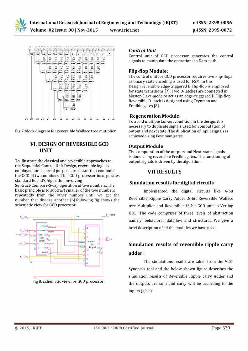
The below table shows the area and Power
comparisons for the digital circuits with 32nm and 92nm
technology.
International Research Journal of Engineering and Technology (IRJET) e-ISSN: 2395-0056
Volume: 02 Issue: 08 | Nov-2015 www.irjet.net p-ISSN: 2395-0072
© 2015, IRJET ISO 9001:2008 Certified Journal Page 341
S.
N
O
Reversible
Digital
circuits
32 nm Technology 90nm Technology
Area Power Area Power
1
2
3
Ripple
carry
adder
Wallace
tree
multiplier
GCD unit
91.157
670
1483.0
50562
3470.8
21809
21.3055
µW
354.7818
µ W
819.7405
µW
273.21
9245
4359.2
86495
12418.
487592
69.846
5µ W
1.4432
e+03
µW
2.8099
e+03µ
W
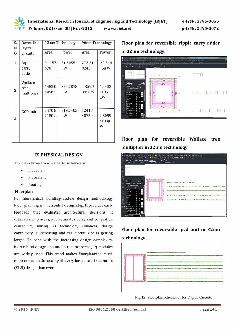
IX PHYSICAL DESIGN
The main three ateps we perform here are:
Floorplan
Placement
Routing
Floorplan
For hierarchical, building-module design methodology
Floor planning is an essential design step. It provides early
feedback that evaluates architectural decisions, it
estimates chip areas, and estimates delay and congestion
caused by wiring. As technology advances, design
complexity is increasing and the circuit size is getting
larger. To cope with the increasing design complexity,
hierarchical design and intellectual property (IP) modules
are widely used. This trend makes floorplanning much
more critical to the quality of a very large-scale integration
(VLSI) design than ever.
Floor plan for reversible ripple carry adder
in 32nm technology:
Floor plan for reversible Wallace tree
multiplier in 32nm technology:
Floor plan for reversible gcd unit in 32nm
technology:
Fig 12: Floorplan schematics for Digital Circuits
International Research Journal of Engineering and Technology (IRJET) e-ISSN: 2395-0056
Volume: 02 Issue: 08 | Nov-2015 www.irjet.net p-ISSN: 2395-0072
© 2015, IRJET ISO 9001:2008 Certified Journal Page 342
Placement
Placement is the process of determining the
locations of circuit devices on a die surface. It is an
important stage in the VLSI design flow, because it affects
routability, performance, heat distribution, and to a less
extent, power consumption of a design. Traditionally, it is
applied after the logic synthesis stage and before the
routing stage. Since the advent of deep submicron process
technology around the mid-1990s, interconnect delay,
which is largely determined by placement, has become the
dominating component of circuit delay. As a result,
placement information is essential, even in early design
stages, to achieve better circuit performance. In recent
years,
Placements for reversible ripple carry
Adder at 32nm technology:
Placement for reversible Wallace tree
multiplier in 32nm technology:
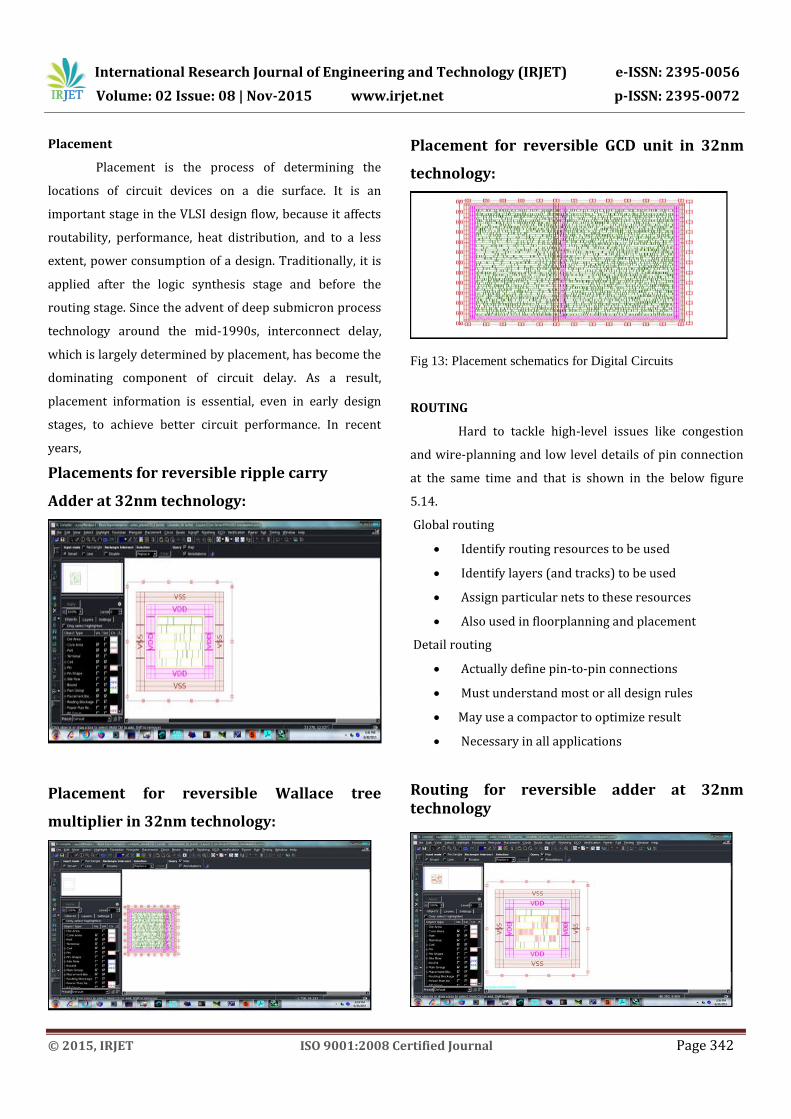
Placement for reversible GCD unit in 32nm
technology:
Fig 13: Placement schematics for Digital Circuits
ROUTING
Hard to tackle high-level issues like congestion
and wire-planning and low level details of pin connection
at the same time and that is shown in the below figure
5.14.
Global routing
Identify routing resources to be used
Identify layers (and tracks) to be used
Assign particular nets to these resources
Also used in floorplanning and placement
Detail routing
Actually define pin-to-pin connections
Must understand most or all design rules
May use a compactor to optimize result
Necessary in all applications
Routing for reversible adder at 32nm technology

International Research Journal of Engineering and Technology (IRJET) e-ISSN: 2395-0056
Volume: 02 Issue: 08 | Nov-2015 www.irjet.net p-ISSN: 2395-0072
© 2015, IRJET ISO 9001:2008 Certified Journal Page 343
Routing for reversible Wallace tree multiplier at 32nm technology
Routing for reversible GCD unit at 32nm technology
Fig 14 :Routingics for Digital Circuits
X. CONLUSION& FUTURE SCOPE
CONLUSION:
In this paper, it can be seen that the performance of
digital circuits can be enhanced using reversible gates and
have compared 8-bit ripple carry reversible adder with
different technologies in terms of speed and power; thereby
concluding that reversible designs are faster and power
efficient. Furthermore, this concept is extended to
combinational circuits such as a Wallace tree multiplier
using reversible gates, which were simulated and respective
results validate prior inferences. Then a reversible
sequential GCD unit was designed.Thus, all the designs
implemented were compared with the 32nm and 90nm
technologies, and the speed and power parameters for the
reversible designs at 32nm technogy were observed to have
improved significantly.
FUTURE SCOPE:
Our future research topic is designing a new reversible gate and to implement reversible logic into a complete Quantum processor capable of ultra-high speed and
infinitesimally low power computing.
XI. REFERENCES [1] Landauer, Rolf, "Irreversibility and heat generation in the computing process," IBM Journal of Research and Development , vol.44, no.1.2, pp.261,269, Jan. 2000 doi: 10.1147/rd.441.0261 [2] Bennett, C.H., "Logical Reversibility of Computation," IBM Journal of Research and Development , vol.17, no.6, pp.525,532, Nov. 1973 doi: 10.1147/rd.176.0525 [3] B, Raghu Kanth; B, Murali Krishna; G, Phani Kumar; J, Poornima,“A Comparative Study of Reversible Logic Gates”, International Journal of VLSI & Signal Processing Applications, vol.2, Issue 1, Feb 2012, (51-55), ISSN 2231-3133 ( Online ). [4] Morrison, M.; Ranganathan, N., "Design of a Reversible ALU Based on Novel Programmable Reversible Logic Gate Structures," VLSI (ISVLSI), 2011 IEEE Computer Society Annual Symposium on , vol., no., pp.126,131, 4-6 July 2011 doi: 10.1109/ISVLSI.2011.30. [5] Nachtigal, M.; Thapliyal, H.; Ranganathan, N., "Design of a reversible single precision floating point multiplier based on operand decomposition," Nanotechnology (IEEE-NANO), 2010 10th IEEE Conference on , vol., no., pp.233,237, 17-20 Aug. 2010 doi: 10.1109/NANO.2010.5697746 (Nachtigal, Thapliyal, & Ranganathan, 2010) [6] John P. Hayes, "Computer Architecture and Organization",McGraw-Hill, 1998. ISBN 10: 0070273553 / ISBN 13: 9780070273559 [7] Min-Lun Chuang; Chun-Yao Wang, "Synthesis of Reversible Sequential Elements," Design Automation Conference, 2007. ASPDAC '07. Asia and South Pacific , vol., no., pp.420,425, 23-26 Jan. 2007 doi: 10.1109/ASPDAC.2007.358022 [8] Yelekar, P.R.; Chiwande, S.S., "Design of sequential circuit using reversible logic," Advances in Engineering, Science and Management (ICAESM), 2012 International Conference on , vol.,
Recommended