TM
Freescale™ and the Freescale logo are trademarks of Freescale Semiconductor, Inc. All other product or service names are the property of their respective owners. © Freescale Semiconductor, Inc. 2009.
AN111
DDR3 Design Considerations for PCB Applications
July 2009
Jon Burnett
TMFreescale Semiconductor Confidential and Proprietary Information. Freescale™ and the Freescale logo are trademarksof Freescale Semiconductor, Inc. All other product or service names are the property of their respective owners. © Freescale Semiconductor, Inc. 2007. 2
Introduction
►Customers are beginning to inquire and / or expect DDR3 support on their new product offerings, especially as the price cross-over point nears.
►The first device with DDR3 support was 8572.
►The first development system with DDR3 will be P2020.
►As such, more and more FSL products are supporting DDR3 moving forward.
►In this session we will look at key distinctions between DDR3 vs. DDR1 & DDR2, with key emphasis placed on elements that are important to hardware / board design engineers.

TMFreescale Semiconductor Confidential and Proprietary Information. Freescale™ and the Freescale logo are trademarksof Freescale Semiconductor, Inc. All other product or service names are the property of their respective owners. © Freescale Semiconductor, Inc. 2007. 3
Overview of Presentation
► DDR3 SDRAM Attributes.
► DDR Controller Highlights.
► DDR3 Signaling.
► DDR3 Routing Methodology.
► Memory Pins, New Features.
► PCB Design Pitfalls.

TMFreescale Semiconductor Confidential and Proprietary Information. Freescale™ and the Freescale logo are trademarksof Freescale Semiconductor, Inc. All other product or service names are the property of their respective owners. © Freescale Semiconductor, Inc. 2007. 4
DDR3 – Same players
► Supported by all major memory vendors
TMFreescale Semiconductor Confidential and Proprietary Information. Freescale™ and the Freescale logo are trademarksof Freescale Semiconductor, Inc. All other product or service names are the property of their respective owners. © Freescale Semiconductor, Inc. 2007. 5
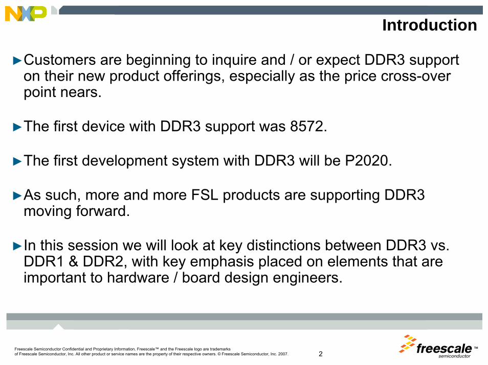
Cross-over Point

TMFreescale Semiconductor Confidential and Proprietary Information. Freescale™ and the Freescale logo are trademarksof Freescale Semiconductor, Inc. All other product or service names are the property of their respective owners. © Freescale Semiconductor, Inc. 2007. 6
DDR SDRAM Highlights and Comparison
Feature/Category DDR1 DDR2 DDR3
Package TSOP BGA only BGA only
512Mb -8Gb
1.5V Core1.5V I/O
SSTL_15
8
800–1600 Mbps
On-die termination for data group. VTT
termination for address, command, and control
Differential
Densities 128Mb -1Gb 256Mb - 4Gb
Voltage 2.5V Core2.5V I/O
1.8V Core1.8V I/O
I/O Signaling SSTL_2 SSTL_18
Internal Memory Banks 4 4 to 8
Data Rate 200-400 Mbps 400–800 Mbps
Termination Motherboard termination to VTT for all signals
On-die termination for data group. VTT
termination for address, command, and control
Data Strobes Single Ended Differential or single

TMFreescale Semiconductor Confidential and Proprietary Information. Freescale™ and the Freescale logo are trademarksof Freescale Semiconductor, Inc. All other product or service names are the property of their respective owners. © Freescale Semiconductor, Inc. 2007. 7
DDR SDRAM Highlights and Comparison (cont.)
Feature/Category DDR1 DDR2 DDR3
Burst Length BL= 2, 4, 8(2-bit prefetch)
BL= 4, 8(4-bit prefetch)
BL= 8 (Burst chop 4)(8-bit prefetch)
CL/tRCD/tRP 15 ns each 15 ns each 12 ns each
Master Reset No No Yes
ODT (On-die termination)
No Yes Yes
Driver Calibration No Off-Chip (OCD) On-Chip with ZQ pin (ZQ cal)
Write Leveling No No Yes

TMFreescale Semiconductor Confidential and Proprietary Information. Freescale™ and the Freescale logo are trademarksof Freescale Semiconductor, Inc. All other product or service names are the property of their respective owners. © Freescale Semiconductor, Inc. 2007. 8
Typical Freescale DDR2/3 Controller Highlights
►Interface speed• DDR2 - up to 800 MHz• DDR3 - up to 800 MHz today (MPC8572, MPC8526)
Evaluating higher speeds 1066 MHz and up to 1600 MHz
►Support Interface width• 64/72-bit data bus – high end product • 32/40-bit data bus – low end products• 16/24-bit data bus – low end products
►Discrete, unbuffered, and registered DIMM support• Memory device densities from 64Mb – through 8Gb• Up to four chip selects supported• Support for x8/x16 DDR devices – x4 devices are not supported
►Full ECC (Error Correction Code) support• Single error correction/detection, double error detection• Error injection for software development
►Self refresh support
TMFreescale Semiconductor Confidential and Proprietary Information. Freescale™ and the Freescale logo are trademarksof Freescale Semiconductor, Inc. All other product or service names are the property of their respective owners. © Freescale Semiconductor, Inc. 2007. 9
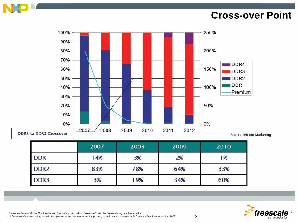
Typical Freescale DDR2/3 Controller Highlights (cont’d)
►Read-Modify-Write support for Atomic Inc, Dec, Set, Clear, and sub-double word writes
►All timing parameters are under SW control►Automatic Data Initialization (easy ECC support)►Differential data strobes►Dedicated Open Row Table for each sub-bank
• Up to 32 simultaneous open rows with 4 chip selects►Up to six diff clock pairs
• Eliminates the need for any external clock PLLs
►ODT support (both internally and externally)►On-chip ZQ driver calibration►SSTL-1.8, and SSTL-1.5 compatible IOs

TMFreescale Semiconductor Confidential and Proprietary Information. Freescale™ and the Freescale logo are trademarksof Freescale Semiconductor, Inc. All other product or service names are the property of their respective owners. © Freescale Semiconductor, Inc. 2007. 10
Memory Controller Block Diagram

TMFreescale Semiconductor Confidential and Proprietary Information. Freescale™ and the Freescale logo are trademarksof Freescale Semiconductor, Inc. All other product or service names are the property of their respective owners. © Freescale Semiconductor, Inc. 2007. 11
Key DDR3 Memory Improvements and Additions
►Lower signaling standard
►Reduced power
► Improved device pinout
►Fly-by architecture
►Write Leveling
►Dynamic ODT for improved Write signaling
►Driver calibration
►Device Reset
►DIMM address mirroring

TMFreescale Semiconductor Confidential and Proprietary Information. Freescale™ and the Freescale logo are trademarksof Freescale Semiconductor, Inc. All other product or service names are the property of their respective owners. © Freescale Semiconductor, Inc. 2007. 12
DDR3 Signaling – Example SSTL-1.5
0.850V
0.765V0.750V0.735V
0.925V
VDDQ (1.5V nominal)
Receiver
VREF + AC NoiseVREF + DC Error
VREF - DC ErrorVREF - AC Noise
0.650V
0.575V
VSSQTransmitter
VOL (MAX)
VOH(MIN)
VIL
VIH
VIHAC
AC
VILDC
DC

TMFreescale Semiconductor Confidential and Proprietary Information. Freescale™ and the Freescale logo are trademarksof Freescale Semiconductor, Inc. All other product or service names are the property of their respective owners. © Freescale Semiconductor, Inc. 2007. 13
Lower Power►Supply voltage reduced from 1.8V to 1.5V
• ~ 30% power reduction (Micron claim)• ~ 25% is JEDEC’s official claim
Compared to DDR2 at same frequency bin
►Lower I/O buffer power• 34 ohm driver vs. 18 ohm driver at memory device
►Improved bandwidth per Watt
DDR2667
DDR2800 DDR3
1067
DDR2533
DDR31333
DDR31600
DDR3800
Pow
er R
elat
ive
to D
DR
2Es
timat
ed
Source: Micron

TMFreescale Semiconductor Confidential and Proprietary Information. Freescale™ and the Freescale logo are trademarksof Freescale Semiconductor, Inc. All other product or service names are the property of their respective owners. © Freescale Semiconductor, Inc. 2007. 14
Improved Pinout
►Improved power delivery• More power and ground balls
►Improved signal quality• Better power & ground
distribution• And better signal referencing
►Fully populated ball grid• Stronger reliability
►Improved pin placement• Less pin skew• Tighter timing leaving chip

TMFreescale Semiconductor Confidential and Proprietary Information. Freescale™ and the Freescale logo are trademarksof Freescale Semiconductor, Inc. All other product or service names are the property of their respective owners. © Freescale Semiconductor, Inc. 2007. 15
Fly By Routing Topology
►Introduction of “Fly-by” architecture • Address, command, control & clocks• Improved signal integrity…enabling higher speeds• On module termination
Controller
VTTFly by routing of clk, command and ctrl
Controller
Matched tree routing of clk command and ctrl
DDR2 DIMM
DDR3 DIMM
TMFreescale Semiconductor Confidential and Proprietary Information. Freescale™ and the Freescale logo are trademarksof Freescale Semiconductor, Inc. All other product or service names are the property of their respective owners. © Freescale Semiconductor, Inc. 2007. 16
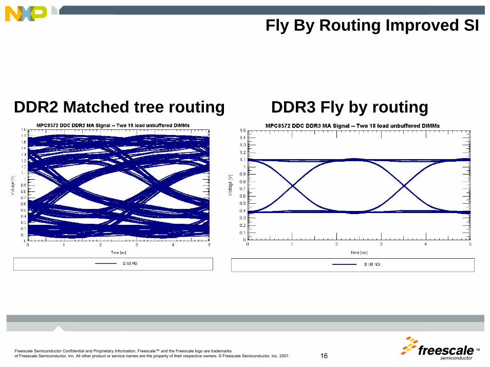
Fly By Routing Improved SI
DDR3 Fly by routingDDR2 Matched tree routing

TMFreescale Semiconductor Confidential and Proprietary Information. Freescale™ and the Freescale logo are trademarksof Freescale Semiconductor, Inc. All other product or service names are the property of their respective owners. © Freescale Semiconductor, Inc. 2007. 17
Fly By Skew Across All receivers
This illustrates the skew created by DDR3 fly by routing

TMFreescale Semiconductor Confidential and Proprietary Information. Freescale™ and the Freescale logo are trademarksof Freescale Semiconductor, Inc. All other product or service names are the property of their respective owners. © Freescale Semiconductor, Inc. 2007. 18
The need for write-leveling….
►tDQSS requirement: • DQS/DQS# rising edge to CK/CK# rising edge• Clock to Strobe should be within a certain range for proper write operation to
DDR3 SDRAMs►tDQSS spec: +/- 0.25*tck

TMFreescale Semiconductor Confidential and Proprietary Information. Freescale™ and the Freescale logo are trademarksof Freescale Semiconductor, Inc. All other product or service names are the property of their respective owners. © Freescale Semiconductor, Inc. 2007. 19
Write-Leveling… How it works
TMFreescale Semiconductor Confidential and Proprietary Information. Freescale™ and the Freescale logo are trademarksof Freescale Semiconductor, Inc. All other product or service names are the property of their respective owners. © Freescale Semiconductor, Inc. 2007. 20
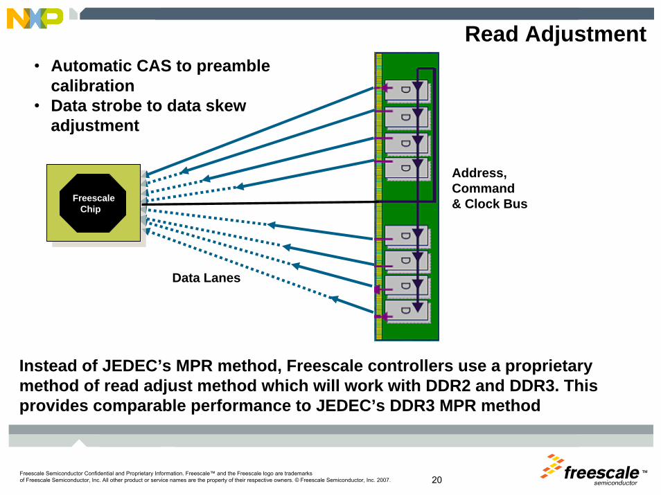
Read Adjustment
FreescaleChip
Address, Command & Clock Bus
Data Lanes
• Automatic CAS to preamble calibration
• Data strobe to data skew adjustment
Instead of JEDEC’s MPR method, Freescale controllers use a proprietary method of read adjust method which will work with DDR2 and DDR3. This provides comparable performance to JEDEC’s DDR3 MPR method

TMFreescale Semiconductor Confidential and Proprietary Information. Freescale™ and the Freescale logo are trademarksof Freescale Semiconductor, Inc. All other product or service names are the property of their respective owners. © Freescale Semiconductor, Inc. 2007. 21
Dynamic ODT – System Motivation Without Dynamic ODT
With Dynamic ODT
Significant improvement of write signal integrity with DDR3 dynamic ODT
Example of termination scheme in application
Write to slot 1
Write to slot 2

TMFreescale Semiconductor Confidential and Proprietary Information. Freescale™ and the Freescale logo are trademarksof Freescale Semiconductor, Inc. All other product or service names are the property of their respective owners. © Freescale Semiconductor, Inc. 2007. 22
New DDR3 Pins
►Introduction of an asynchronous RESET# pin• Prevent Illegal commands and/or unwanted states
Cold resetWarm reset
• Known initializationResets all state informationNo power-down requiredDestructive to data contents

TMFreescale Semiconductor Confidential and Proprietary Information. Freescale™ and the Freescale logo are trademarksof Freescale Semiconductor, Inc. All other product or service names are the property of their respective owners. © Freescale Semiconductor, Inc. 2007. 23
New DDR3 Pins… cont’d
►VREF broken into separate banks (..at the DDR3 memories)• VREFCA
Used for the command / address signalsDecoupled to VDD plane
• VREFDQUsed for the data signalsDecoupled to VDD plane
►Key premise – Noise reduction and coupling between the groups
At the DDR3 controller the same source driving VREFDQ to the memories would drive the controller VREF pin.

TMFreescale Semiconductor Confidential and Proprietary Information. Freescale™ and the Freescale logo are trademarksof Freescale Semiconductor, Inc. All other product or service names are the property of their respective owners. © Freescale Semiconductor, Inc. 2007. 24
NEW DDR3 pins – ZQ Calibration Pin
►The RZQ resistor is connected between the DDR3 memory and ground• Value = 240 Ohm +/- 1%• Permits driver and ODT calibration over process, voltage, and temperatures
►Easier and more accepted than DDR2’s (optional) OCD method.
►Our controllers support both ZQ calibration commands• ZQCL – used during initialization (..takes longer)• ZQCS – used during normal operation (…periodic and takes less time)

TMFreescale Semiconductor Confidential and Proprietary Information. Freescale™ and the Freescale logo are trademarksof Freescale Semiconductor, Inc. All other product or service names are the property of their respective owners. © Freescale Semiconductor, Inc. 2007. 25
Freescale Controller Driver Calibration
►Our Freescale controller also does driver calibration• Enabled by software• Occurs automatically during initialization after MEM_EN is set
►MDIC precision resistors are used at our controller• Value = 40 Ohms 1% tolerance

TMFreescale Semiconductor Confidential and Proprietary Information. Freescale™ and the Freescale logo are trademarksof Freescale Semiconductor, Inc. All other product or service names are the property of their respective owners. © Freescale Semiconductor, Inc. 2007. 26
DIMM Mirroring…
►The DDR3 IP fully supports address mirroring
Non-Mirrored Mirrored

TMFreescale Semiconductor Confidential and Proprietary Information. Freescale™ and the Freescale logo are trademarksof Freescale Semiconductor, Inc. All other product or service names are the property of their respective owners. © Freescale Semiconductor, Inc. 2007. 27
NEW DDR3 pins – TDQS/TDQS#
►TDQS/TDQS# New pin on x8 DDR3 devices• Not present on x4 or x16 devices• Allows combinations of x4/x8 devices in the same system.
►We don’t support TDQS/TDQS# • We do not support x4 devices… so this function is not supported

TMFreescale Semiconductor Confidential and Proprietary Information. Freescale™ and the Freescale logo are trademarksof Freescale Semiconductor, Inc. All other product or service names are the property of their respective owners. © Freescale Semiconductor, Inc. 2007. 28
Layout Example – CTS8536
►Byte lane routing example

TMFreescale Semiconductor Confidential and Proprietary Information. Freescale™ and the Freescale logo are trademarksof Freescale Semiconductor, Inc. All other product or service names are the property of their respective owners. © Freescale Semiconductor, Inc. 2007. 29
DDR3-800Mhz In the Lab
Good margins across all data beats
120 Ohm / Half Driver / 1 DIMM
RequiredTsu = 95 psTh = 170 ps

TMFreescale Semiconductor Confidential and Proprietary Information. Freescale™ and the Freescale logo are trademarksof Freescale Semiconductor, Inc. All other product or service names are the property of their respective owners. © Freescale Semiconductor, Inc. 2007. 30
Common Design Pitfalls

TMFreescale Semiconductor Confidential and Proprietary Information. Freescale™ and the Freescale logo are trademarksof Freescale Semiconductor, Inc. All other product or service names are the property of their respective owners. © Freescale Semiconductor, Inc. 2007. 31
Design Pitfalls Summary
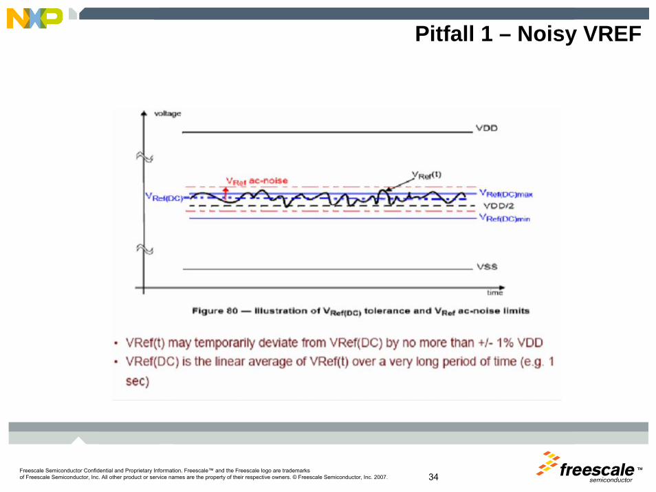
►Pitfall 1 Noisy Vref: Care must be taken to isolate Vref►Pitfall 2 Weak Vref: Insure adequate current for Vref►Pitfall 3 Ref Plane: Insure excellent reference plane for all DDR
signals►Pitfall 4 Data Tuning: Data bits within 10 mil, Byte lanes within 0.5”►Pitfall 5 Proper Termination: Discrete implementations require term.►Pitfall 6 POR Config: Insure correct DDR (2/3) is set for controller►Pitfall 7 Expandability: Hook up unused address lines►Pitfall 8 Incorrect Topology: Insure use of JEDEC routing topologies►Pitfall 9 Separate VDDQ/VDDIO : VDDQ and VDDIO are common
on DDR DIMM Modules, not on controller.

TMFreescale Semiconductor Confidential and Proprietary Information. Freescale™ and the Freescale logo are trademarksof Freescale Semiconductor, Inc. All other product or service names are the property of their respective owners. © Freescale Semiconductor, Inc. 2007. 32
Design Pitfalls Summary (Continued)
►Pitfall 10 Slew Rate: Must account for de-rated slew rate for system timing (See JEDEC Table)
►Pitfall 11 Testability: Insure there is test and measurement access to DDR signals
►Some other noteworthy pitfalls • Not using ECC
Highly Recommended for first prototypes. De-pop for production• Missing pull-up on MAPAR_ERR (registered DIMMs) and MAPAR_OUT
TMFreescale Semiconductor Confidential and Proprietary Information. Freescale™ and the Freescale logo are trademarksof Freescale Semiconductor, Inc. All other product or service names are the property of their respective owners. © Freescale Semiconductor, Inc. 2007. 33
Design PitfallsBackup Slides
TMFreescale Semiconductor Confidential and Proprietary Information. Freescale™ and the Freescale logo are trademarksof Freescale Semiconductor, Inc. All other product or service names are the property of their respective owners. © Freescale Semiconductor, Inc. 2007. 34
Pitfall 1 – Noisy VREF

TMFreescale Semiconductor Confidential and Proprietary Information. Freescale™ and the Freescale logo are trademarksof Freescale Semiconductor, Inc. All other product or service names are the property of their respective owners. © Freescale Semiconductor, Inc. 2007. 35
Pitfall 1 – Measuring VREF
►Measuring at device will likely give greater than 50 mV peak-to-peak• Result of coupled noise from DDR device
►VREF system noise should be measured at capacitor nearest the memory device
VREF on device
VREF at Decoupling cap

TMFreescale Semiconductor Confidential and Proprietary Information. Freescale™ and the Freescale logo are trademarksof Freescale Semiconductor, Inc. All other product or service names are the property of their respective owners. © Freescale Semiconductor, Inc. 2007. 36
Pitfall 1 – Protecting VREF

TMFreescale Semiconductor Confidential and Proprietary Information. Freescale™ and the Freescale logo are trademarksof Freescale Semiconductor, Inc. All other product or service names are the property of their respective owners. © Freescale Semiconductor, Inc. 2007. 37
Pitfall 2 – Wimpy VREF source
►VREF current consumption is typically 1.5-2.0 mA►For most DDR regulators…. this is easily handled
0.75

TMFreescale Semiconductor Confidential and Proprietary Information. Freescale™ and the Freescale logo are trademarksof Freescale Semiconductor, Inc. All other product or service names are the property of their respective owners. © Freescale Semiconductor, Inc. 2007. 38
Pitfall 3 – Reference Plane discontinuities
►Contiguous reference plane• GND – Data• Pwr - Address / Cmd
►Use stitching vias if switching layers
►Keep away from plane voids►Avoid crossing plane splits►Avoid trace over anti-pad
Gnd stitching via
Plane Void
Long Trace Routes

TMFreescale Semiconductor Confidential and Proprietary Information. Freescale™ and the Freescale logo are trademarksof Freescale Semiconductor, Inc. All other product or service names are the property of their respective owners. © Freescale Semiconductor, Inc. 2007. 39
Pitfall 4 – Data Tuning
Within byte lane +/- 10mil
Across all byte lanes match to within 0.5
inches

TMFreescale Semiconductor Confidential and Proprietary Information. Freescale™ and the Freescale logo are trademarksof Freescale Semiconductor, Inc. All other product or service names are the property of their respective owners. © Freescale Semiconductor, Inc. 2007. 40
Pitfall 5 – Forgetting Termination
Still needed for soldered-down implementations.
DIMM modules have the termination on the module.
TMFreescale Semiconductor Confidential and Proprietary Information. Freescale™ and the Freescale logo are trademarksof Freescale Semiconductor, Inc. All other product or service names are the property of their respective owners. © Freescale Semiconductor, Inc. 2007. 41
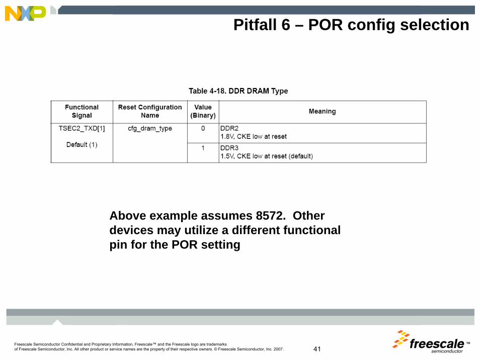
Pitfall 6 – POR config selection
Above example assumes 8572. Other devices may utilize a different functional pin for the POR setting

TMFreescale Semiconductor Confidential and Proprietary Information. Freescale™ and the Freescale logo are trademarksof Freescale Semiconductor, Inc. All other product or service names are the property of their respective owners. © Freescale Semiconductor, Inc. 2007. 42
Pitfall 7 – Expandability
Rule of thumb:For DDR3 - Every address (A0-A15), and all three bank address (BA0-BA2) line from our controllers should be connected to the memory subsystem.
SignalName
PinNomenclature
Signal Type Function
A13 NC No connection to internal die.Okay to run trace to PCB pad.
Used on x4/x8 512 Mb and 1 Gb devices and all configurations of the 2 Gb or 4Gb.
A14 NC No connection to internal die.Okay to run trace to PCB pad.
Used on x4/x8 2 Gb devices and all 4 Gb configurations.
A15 NC No connection to internal die.Okay to run trace to PCB pad.
Used on 4 Gb (x4/x8).
BA2 NC No connection to internal die.Okay to run trace to PCB pad.
Used on all configurations of the 1 Gb, 2 Gb, and 4 Gb.

TMFreescale Semiconductor Confidential and Proprietary Information. Freescale™ and the Freescale logo are trademarksof Freescale Semiconductor, Inc. All other product or service names are the property of their respective owners. © Freescale Semiconductor, Inc. 2007. 43
Pitfall 8 – Not using proven JEDEC topologies

TMFreescale Semiconductor Confidential and Proprietary Information. Freescale™ and the Freescale logo are trademarksof Freescale Semiconductor, Inc. All other product or service names are the property of their respective owners. © Freescale Semiconductor, Inc. 2007. 44
Pitfall 9 – Separate VDDQ/VDDIO
VDDQ(io pwr)
VDD(ddr pwr)
PowerQUICC®
Controller
Separate planes are not viable with standard
JEDEC DIMM memory modules
VDDQ & VDDIO are same plane on the modules

TMFreescale Semiconductor Confidential and Proprietary Information. Freescale™ and the Freescale logo are trademarksof Freescale Semiconductor, Inc. All other product or service names are the property of their respective owners. © Freescale Semiconductor, Inc. 2007. 45
Pitfall 10– Slew Rate De-rating (setup & hold)
Source: Xcell Journal
Source: JEDEC 79-2C

TMFreescale Semiconductor Confidential and Proprietary Information. Freescale™ and the Freescale logo are trademarksof Freescale Semiconductor, Inc. All other product or service names are the property of their respective owners. © Freescale Semiconductor, Inc. 2007. 46
Pitfall 11 – No debug or testability on BGA devices

TMFreescale Semiconductor Confidential and Proprietary Information. Freescale™ and the Freescale logo are trademarksof Freescale Semiconductor, Inc. All other product or service names are the property of their respective owners. © Freescale Semiconductor, Inc. 2007. 47
Power up and Initialization SequenceBackup Slides

TMFreescale Semiconductor Confidential and Proprietary Information. Freescale™ and the Freescale logo are trademarksof Freescale Semiconductor, Inc. All other product or service names are the property of their respective owners. © Freescale Semiconductor, Inc. 2007. 48
DDR3 Initialization Flow Power-up
DDRReset
DDR CTRLINIT
Chip selects enabled and DDR clocks begin
Asserted atleast 200us
StableCLKS
CKE = HIGH
DRAMsInitialized
Mode Register Commands Issued
ZQCalibration
Write Leveling
ReadAdjust
ControllerStarted
MEM_EN =1
Automatic CAS-to-Preamble (aka Read Leveling)….
Plus Data-to-Strobe adjustment
ZQCL Issued (512 clocks)Also DLL lock time is occuring
InitComplete Ready for User accesses
Automatically handledBy the controller
DDR3’s ConductPrechargeNeed at
least 500us from reset deassertionto the controller being enabled.
Timed loop may be needed.
TMFreescale Semiconductor Confidential and Proprietary Information. Freescale™ and the Freescale logo are trademarksof Freescale Semiconductor, Inc. All other product or service names are the property of their respective owners. © Freescale Semiconductor, Inc. 2007. 49
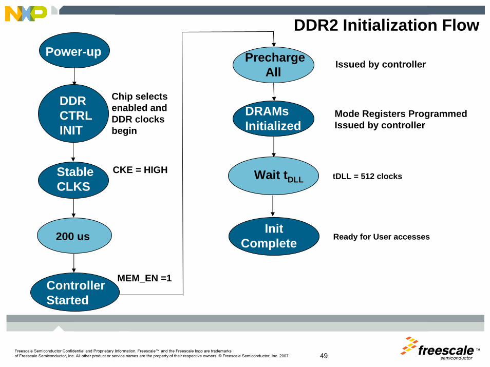
DDR2 Initialization Flow Power-up
DDR CTRLINIT
Chip selects enabled and DDR clocks begin
StableCLKS
CKE = HIGH
DRAMsInitialized
DQS Adjust
ReadCalibration
ReadAdjust
Mode Registers ProgrammedIssued by controller
ControllerStarted
MEM_EN =1
InitComplete Ready for User accesses
PrechargeAll
Issued by controller
200 us
DQS Adjust
Wait tDLL tDLL = 512 clocks

TMFreescale Semiconductor Confidential and Proprietary Information. Freescale™ and the Freescale logo are trademarksof Freescale Semiconductor, Inc. All other product or service names are the property of their respective owners. © Freescale Semiconductor, Inc. 2007. 50
Burst Length
►Burst Length control (BC4/8 on the fly)• 8-bit pre-fetch is standard for DDR3 memories• Thus, burst length of 8 is default
►DDR3’s also support ‘pseudo BL4’ using burst chip
Memory
IO
166 MHz
667 Mhz
8-bits at once
1333 Mbps
D D D D D D D D D D D D D D D D
D D D D D D D D D D D D D D D D
BL8
Burst Chop 4A12 = High
Read Read
bubble bubble

TMFreescale Semiconductor Confidential and Proprietary Information. Freescale™ and the Freescale logo are trademarksof Freescale Semiconductor, Inc. All other product or service names are the property of their respective owners. © Freescale Semiconductor, Inc. 2007. 51
Power-up : Power Rails
►DDR3 memories have two power pins defined. • Same voltage level of 1.5V nominal• Separate pins help reduce power supply noise/interruption• VDD – Core Power• VDDQ – IO Power
►Therefore, there will be 2 different cases:• Case 1 – two separate sources• Case 2 – Single voltage source for both rails

TMFreescale Semiconductor Confidential and Proprietary Information. Freescale™ and the Freescale logo are trademarksof Freescale Semiconductor, Inc. All other product or service names are the property of their respective owners. © Freescale Semiconductor, Inc. 2007. 52
Power-up : Power Rails cont’d
►The following should be applied whether a single voltage source or a separate voltage sources are used:
• Apply Power:RESET# is recommended to be maintained below 0.2V X VDD (min 200us) and all other inputs may be undefined
• The voltage ramp time between 300mV to VDDmin must be no greater than 200ms
VDD > VDDQ, VDD-VDDQ < 0.3V• The voltage levels on all other pins should not exceed VDD/VDDQ or be
below VSS/VSSQ

TMFreescale Semiconductor Confidential and Proprietary Information. Freescale™ and the Freescale logo are trademarksof Freescale Semiconductor, Inc. All other product or service names are the property of their respective owners. © Freescale Semiconductor, Inc. 2007. 53
Reset
►Starting with DDR3, a reset function is supported• All devices have a dedicated RESET# pin, operating at CMOS levels• Low pass filter incorporated – prevents accidental glitches• Voltage level of the pin should be carefully maintained to prevent loss of
data
►Reset should be done after the power supply voltage level(s) are properly up and stabilized
►Reset can also be issued whenever “Warm-booting” is needed.
►Destructive to data contents, therefore memories will need to be re-initialized

TMFreescale Semiconductor Confidential and Proprietary Information. Freescale™ and the Freescale logo are trademarksof Freescale Semiconductor, Inc. All other product or service names are the property of their respective owners. © Freescale Semiconductor, Inc. 2007. 54
Stable clocks
►Clocks are started as soon as a chip select is enabled. • Controller will ensure that the appropriate clock to
CKE relationship is met

TMFreescale Semiconductor Confidential and Proprietary Information. Freescale™ and the Freescale logo are trademarksof Freescale Semiconductor, Inc. All other product or service names are the property of their respective owners. © Freescale Semiconductor, Inc. 2007. 55
DRAMs Initialized
►Once clocks are stabilized, the next step should be to set the Mode Register.
• Mode Registers set the operational mode of the DDR3 DRAMs• Order of programming
MR2 -> MR3 -> MR1 -> MR0
►Several new features for DDR3, such as • MR0 : Burst length control (BC4/8 on the fly)• MR1 : Write leveling enable• MR2 : RTT_WR, CWL, ASR

TMFreescale Semiconductor Confidential and Proprietary Information. Freescale™ and the Freescale logo are trademarksof Freescale Semiconductor, Inc. All other product or service names are the property of their respective owners. © Freescale Semiconductor, Inc. 2007. 56
Mode Register Set 0

TMFreescale Semiconductor Confidential and Proprietary Information. Freescale™ and the Freescale logo are trademarksof Freescale Semiconductor, Inc. All other product or service names are the property of their respective owners. © Freescale Semiconductor, Inc. 2007. 57
Mode Register Set 1

TMFreescale Semiconductor Confidential and Proprietary Information. Freescale™ and the Freescale logo are trademarksof Freescale Semiconductor, Inc. All other product or service names are the property of their respective owners. © Freescale Semiconductor, Inc. 2007. 58
Mode Register Set 2
TMFreescale Semiconductor Confidential and Proprietary Information. Freescale™ and the Freescale logo are trademarksof Freescale Semiconductor, Inc. All other product or service names are the property of their respective owners. © Freescale Semiconductor, Inc. 2007. 59
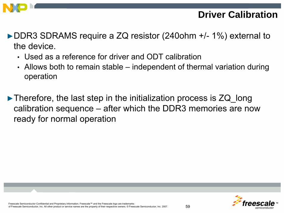
Driver Calibration
►DDR3 SDRAMS require a ZQ resistor (240ohm +/- 1%) external to the device.
• Used as a reference for driver and ODT calibration• Allows both to remain stable – independent of thermal variation during
operation
►Therefore, the last step in the initialization process is ZQ_longcalibration sequence – after which the DDR3 memories are now ready for normal operation

TM
Recommended