32” LCD TV/DVDchassis FL11.11
© 2011 Funai Electric Co., Ltd.
All rights reserved. No part of this manual may be reproduced, copied, transmitted, disseminated, transcribed, downloaded or stored in any storage medium, in any form or for any purpose without the express prior written consent of Funai. Furthermore, any unauthorized commercial distribution of this manual or any revision hereto is strictly prohibited.
Information in this document is subject to change without notice. Funai reserves the right to change the content herein without the obligation to notify any person or organization of such changes.
with the design is a registered trademark of Funai Electric Co., Ltd and may not be used in any way without the express written consent of Funai. All other trademarks used herein remain the exclusive property of their respective owners. Nothing contained in this manual should be construed as granting, by implication or otherwise, any license or right to use any of the trademarks displayed herein. Misuse of any trademarks or any other content in this manual is strictly prohibited. Funai shall aggressively enforce its intellectual property rights to the fullest extent of the law.
SERVICE MANUALContents
TYPE ALD320SS2 SYLVANIA (Serial No.: DS1)
32MD301B/F7 MAGNAVOX (Serial No.: DS1)
32MD311B/F7 MAGNAVOX (Serial No.: DS1)
This service manual contains information of different types of models.Make sure to refer to the section describing your model.
110427

IMPORTANT SAFETY NOTICE
Proper service and repair is important to the safe, reliable operation of all Funai Equipment. The service procedures recommended by Funai and described in this service manual are effective methods of performing service operations. Some of these service special tools should be used when and as recommended.
It is important to note that this service manual contains various CAUTIONS and NOTICES which should be carefully read in order to minimize the risk of personal injury to service personnel. The possibility exists that improper service methods may damage the equipment. It also is important to understand that these CAUTIONS and NOTICES ARE NOT EXHAUSTIVE. Funai could not possibly know, evaluate and advice the service trade of all conceivable ways in which service might be done or of the possible hazardous consequences of each way. Consequently, Funai has not undertaken any such broad evaluation. Accordingly, a servicer who uses a service procedure or tool which is not recommended by Funai must first use all precautions thoroughly so that neither his safety nor the safe operation of the equipment will be jeopardized by the service method selected.
The LCD panel is manufactured to provide many years of useful life. Occasionally a few non active pixels may appear as a tiny spec of color. This is not to be considered a defect in the LCD screen.
Manufactured under license from Dolby Laboratories. Dolby and the double-D symbol are trademarks of Dolby Laboratories.

TABLE OF CONTENTS
Specifications . . . . . . . . . . . . . . . . . . . . . . . . . . . . . . . . . . . . . . . . . . . . . . . . . . . . . . . . . . . . . . . . . . . . . . . . . . . 1-1Laser Beam Safety Precautions . . . . . . . . . . . . . . . . . . . . . . . . . . . . . . . . . . . . . . . . . . . . . . . . . . . . . . . . . . . . . 2-1Important Safety Precautions . . . . . . . . . . . . . . . . . . . . . . . . . . . . . . . . . . . . . . . . . . . . . . . . . . . . . . . . . . . . . . . 3-1Standard Notes for Servicing . . . . . . . . . . . . . . . . . . . . . . . . . . . . . . . . . . . . . . . . . . . . . . . . . . . . . . . . . . . . . . . 4-1Cabinet Disassembly Instructions . . . . . . . . . . . . . . . . . . . . . . . . . . . . . . . . . . . . . . . . . . . . . . . . . . . . . . . . . . . 5-1Electrical Adjustment Instructions . . . . . . . . . . . . . . . . . . . . . . . . . . . . . . . . . . . . . . . . . . . . . . . . . . . . . . . . . . . . 6-1 How to Initialize the LCD TV/DVD. . . . . . . . . . . . . . . . . . . . . . . . . . . . . . . . . . . . . . . . . . . . . . . . . . . . . . . . . . . . 7-1Firmware Renewal Mode . . . . . . . . . . . . . . . . . . . . . . . . . . . . . . . . . . . . . . . . . . . . . . . . . . . . . . . . . . . . . . . . . . 8-1 Troubleshooting. . . . . . . . . . . . . . . . . . . . . . . . . . . . . . . . . . . . . . . . . . . . . . . . . . . . . . . . . . . . . . . . . . . . . . . . . . 9-1Block Diagrams . . . . . . . . . . . . . . . . . . . . . . . . . . . . . . . . . . . . . . . . . . . . . . . . . . . . . . . . . . . . . . . . . . . . . . . . 10-1Schematic Diagrams / CBA and Test Points . . . . . . . . . . . . . . . . . . . . . . . . . . . . . . . . . . . . . . . . . . . . . . . . . . . 11-1Waveforms . . . . . . . . . . . . . . . . . . . . . . . . . . . . . . . . . . . . . . . . . . . . . . . . . . . . . . . . . . . . . . . . . . . . . . . . . . . . 12-1Wiring Diagram . . . . . . . . . . . . . . . . . . . . . . . . . . . . . . . . . . . . . . . . . . . . . . . . . . . . . . . . . . . . . . . . . . . . . . . . . 13-1System Control Timing Charts . . . . . . . . . . . . . . . . . . . . . . . . . . . . . . . . . . . . . . . . . . . . . . . . . . . . . . . . . . . . . 14-1Lead Identifications . . . . . . . . . . . . . . . . . . . . . . . . . . . . . . . . . . . . . . . . . . . . . . . . . . . . . . . . . . . . . . . . . . . . . . 15-1Exploded Views. . . . . . . . . . . . . . . . . . . . . . . . . . . . . . . . . . . . . . . . . . . . . . . . . . . . . . . . . . . . . . . . . . . . . . . . . 16-1Parts List . . . . . . . . . . . . . . . . . . . . . . . . . . . . . . . . . . . . . . . . . . . . . . . . . . . . . . . . . . . . . . . . . . . . . . . . . . . . . . 17-1Revision History . . . . . . . . . . . . . . . . . . . . . . . . . . . . . . . . . . . . . . . . . . . . . . . . . . . . . . . . . . . . . . . . . . . . . . . . 18-1

1-1 FL11.11SP
SPECIFICATIONS
< LCD TV Section >
< TUNER / NTSC >ANT. Input ---------------------- 75 Ω Unbal., F type
< TUNER / ATSC >
< LCD PANEL >
< VIDEO >
< AUDIO >All items are measured across 8 Ω load at speaker output terminal with L.P.F.
Description Condition Unit Nominal Limit
1. AFT Pull-In Range --- MHz ±2.3 ±2.1
2. Synchronizing Sens.TV.ch.4
CA.ch.31CA.ch.87
dBµdBµdBµ
181818
202023
Description Condition Unit Nominal Limit
1. Received Freq. Range (-28dBm) --- kHz --- ±100
2. ATSC Dynamic Range (min / max)ch.4ch.10ch.41
dBmdBmdBm
---------
-76/0-76/0
-76/+4
Description Condition Unit Nominal Limit
1. Native Pixel Resolution HorizontalVertical
pixelspixels
1366768
------
2. Brightness (w / filter) --- cd/m2 310 ---
3. Viewing Angle HorizontalVertical
°°
-88 to 88-88 to 88
------
Description Condition Unit Nominal Limit
1. Over Scan HorizontalVertical
%%
55
5±55±5
2. Color Temperature---xy
°K 120000.2720.278
---±3%±3%
3. Resolution (composite video) HorizontalVertical
lineline
400350
------
Description Condition Unit Nominal Limit
1. Audio Output 10% Distortion (ATSC 0 dBfs) Lch/Rch W 10.0/10.0 9.0/9.0
2. Audio Distortion (NTSC) 500mW: Lch/Rch % 0.5/0.5 2.0/2.0
3. Audio Freq. Response (NTSC) -6dB: Lch-6dB: Rch
HzHz
70 to 10 k70 to 10 k
------
1-2 FL11.11SP
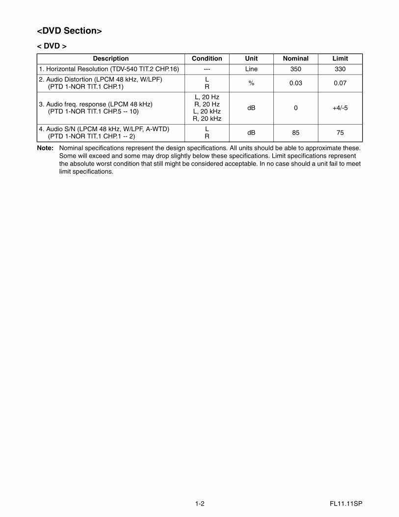
<DVD Section>
< DVD >
Note: Nominal specifications represent the design specifications. All units should be able to approximate these. Some will exceed and some may drop slightly below these specifications. Limit specifications represent the absolute worst condition that still might be considered acceptable. In no case should a unit fail to meet limit specifications.
Description Condition Unit Nominal Limit
1. Horizontal Resolution (TDV-540 TIT.2 CHP.16) --- Line 350 330
2. Audio Distortion (LPCM 48 kHz, W/LPF) (PTD 1-NOR TIT.1 CHP.1)
LR % 0.03 0.07
3. Audio freq. response (LPCM 48 kHz) (PTD 1-NOR TIT.1 CHP.5 -- 10)
L, 20 HzR, 20 HzL, 20 kHzR, 20 kHz
dB 0 +4/-5
4. Audio S/N (LPCM 48 kHz, W/LPF, A-WTD) (PTD 1-NOR TIT.1 CHP.1 -- 2)
LR dB 85 75

2-1 TVDVDN_LBSP(1EM435619)(A1DA1UH).fm
LASER BEAM SAFETY PRECAUTIONS
This DVD player uses a pickup that emits a laser beam.
The laser beam is emitted from the location shown in the figure. When checking the laser diode, be sure to keep your eyes at least 11.8 inches (30 cm) away from the pickup lens when the diode is turned on. Do not look directly at the laser beam.
CAUTION: Use of controls and adjustments, or doing procedures other than those specified herein, may result in hazardous radiation exposure.
Location: Top of LCD Module
Do not look directly at the laser beam coming from the pickup or allow it to strike against your skin.
Drive Mechanism Assembly
Laser Beam Radiation
Laser Pickup
Turntable

3-1 LTVN_ISP
IMPORTANT SAFETY PRECAUTIONS
Prior to shipment from the factory, our products are strictly inspected for recognized product safety and electrical codes of the countries in which they are to be sold. However, in order to maintain such compliance, it is equally important to implement the following precautions when a set is being serviced.
Safety Precautions for LCD TV Circuit1. Before returning an instrument to the
customer, always make a safety check of the entire instrument, including, but not limited to, the following items:
a. Be sure that no built-in protective devices are defective and have been defeated during servicing. (1) Protective shields are provided on this chassis to protect both the technician and the customer. Correctly replace all missing protective shields, including any removed for servicing convenience. (2) When reinstalling the chassis and/or other assembly in the cabinet, be sure to put back in place all protective devices, including but not limited to, nonmetallic control knobs, insulating fishpapers, adjustment and compartment covers/shields, and isolation resistor/capacitor networks. Do not operate this instrument or permit it to be operated without all protective devices correctly installed and functioning. Servicers who defeat safety features or fail to perform safety checks may be liable for any resulting damage.
b. Be sure that there are no cabinet openings through which an adult or child might be able to insert their fingers and contact a hazardous voltage. Such openings include, but are not limited to, (1) spacing between the Liquid Crystal Panel and the cabinet mask, (2) excessively wide cabinet ventilation slots, and (3) an improperly fitted and/or incorrectly secured cabinet back cover.
c. Antenna Cold Check - With the instrument AC plug removed from any AC source, connect an electrical jumper across the two AC plug prongs. Place the instrument AC switch in the on position. Connect one lead of an ohmmeter to the AC plug prongs tied together and touch the other ohmmeter lead in turn to each tuner antenna input exposed terminal screw and, if applicable, to the coaxial connector. If the measured resistance is less than 1.0 megohm or greater than 5.2 megohm, an abnormality exists that must be corrected before the instrument is returned to the customer. Repeat this test with the instrument AC switch in the off position.
d. Leakage Current Hot Check - With the instrument completely reassembled, plug the AC line cord directly into a 120 V AC outlet. (Do not use an isolation transformer during this test.) Use a leakage current tester or a metering system that complies with American National Standards Institute (ANSI) C101.1 Leakage Current for Appliances and Underwriters Laboratories (UL) 1410, (50.7). With the instrument AC switch first in the on position and then in the off position, measure from a known earth ground (metal water pipe, conduit, etc.) to all exposed metal parts of the instrument (antennas, handle brackets, metal cabinet, screw heads, metallic overlays, control shafts, etc.), especially any exposed metal parts that offer an electrical return path to the chassis. Any current measured must not exceed 0.5 milli-ampere. Reverse the instrument power cord plug in the outlet and repeat the test.
ANY MEASUREMENTS NOT WITHIN THE LIMITS SPECIFIED HEREIN INDICATE A POTENTIAL SHOCK HAZARD THAT MUST BE ELIMINATED BEFORE RETURNING THE INSTRUMENT TO THE CUSTOMER OR BEFORE CONNECTING THE ANTENNA OR ACCESSORIES.
2. Read and comply with all caution and safety-related notes on or inside the receiver cabinet, on the receiver chassis, or on the Liquid Crystal Panel.
ALSO TEST WITHPLUG REVERSEDUSING ACADAPTER PLUGAS REQUIRED
TEST ALL EXPOSEDMETAL SURFACES
READING SHOULD NOT BE ABOVE 0.5 mA
EARTHGROUND
_
DEVICELEAKAGECURRENT
TESTER
+BEINGTESTED

3-2 LTVN_ISP
3. Design Alteration Warning - Do not alter or add to the mechanical or electrical design of this TV receiver. Design alterations and additions, including, but not limited to circuit modifications and the addition of items such as auxiliary audio and/or video output connections, might alter the safety characteristics of this receiver and create a hazard to the user. Any design alterations or additions will void the manufacturer's warranty and may make you, the servicer, responsible for personal injury or property damage resulting therefrom.
4. Hot Chassis Warning -
a. Some TV receiver chassis are electrically connected directly to one conductor of the AC power cord and maybe safety-serviced without an isolation transformer only if the AC power plug is inserted so that the chassis is connected to the ground side of the AC power source. To confirm that the AC power plug is inserted correctly, with an AC voltmeter, measure between the chassis and a known earth ground. If a voltage reading in excess of 1.0 V is obtained, remove and reinsert the AC power plug in the opposite polarity and again measure the voltage potential between the chassis and a known earth ground.
b. Some TV receiver chassis normally have 85V AC(RMS) between chassis and earth ground regardless of the AC plug polarity. This chassis can be safety-serviced only with an isolation transformer inserted in the power line between the receiver and the AC power source, for both personnel and test equipment protection.
c. Some TV receiver chassis have a secondary ground system in addition to the main chassis ground. This secondary ground system is not isolated from the AC power line. The two ground systems are electrically separated by insulation material that must not be defeated or altered.
5. Observe original lead dress. Take extra care to assure correct lead dress in the following areas: a. near sharp edges, b. near thermally hot parts-be sure that leads and components do not touch thermally hot parts, c. the AC supply, d. high voltage, and, e. antenna wiring. Always inspect in all areas for pinched, out of place, or frayed wiring. Check AC power cord for damage.
6. Components, parts, and/or wiring that appear to have overheated or are otherwise damaged should be replaced with components, parts, or wiring that meet original specifications. Additionally, determine the cause of overheating and/or damage and, if necessary, take corrective action to remove any potential safety hazard.
7. Product Safety Notice - Some electrical and mechanical parts have special safety-related characteristics which are often not evident from visual inspection, nor can the protection they give necessarily be obtained by replacing them with components rated for higher voltage, wattage, etc. Parts that have special safety characteristics are identified by a # on schematics and in parts lists. Use of a substitute replacement that does not have the same safety characteristics as the recommended replacement part might create shock, fire, and/or other hazards. The product's safety is under review continuously and new instructions are issued whenever appropriate. Prior to shipment from the factory, our products are strictly inspected to confirm they comply with the recognized product safety and electrical codes of the countries in which they are to be sold. However, in order to maintain such compliance, it is equally important to implement the following precautions when a set is being serviced.

3-3 LTVN_ISP
Precautions during ServicingA. Parts identified by the # symbol are critical for
safety.Replace only with part number specified.
B. In addition to safety, other parts and assemblies are specified for conformance with regulations applying to spurious radiation. These must also be replaced only with specified replacements.Examples: RF converters, RF cables, noise blocking capacitors, and noise blocking filters, etc.
C. Use specified internal wiring. Note especially:
1) Wires covered with PVC tubing
2) Double insulated wires
3) High voltage leads
D. Use specified insulating materials for hazardous live parts. Note especially:
1) Insulation Tape
2) PVC tubing
3) Spacers
4) Insulators for transistors.
E. When replacing AC primary side components (transformers, power cord, etc.), wrap ends of wires securely about the terminals before soldering.
F. Observe that the wires do not contact heat producing parts (heat sinks, oxide metal film resistors, fusible resistors, etc.)
G. Check that replaced wires do not contact sharp edged or pointed parts.
H. When a power cord has been replaced, check that 11~13 lb (5~6 kg) of force in any direction will not loosen it.
I. Also check areas surrounding repaired locations.
J. Use care that foreign objects (screws, solder droplets, etc.) do not remain inside the set.
K. When connecting or disconnecting the internal connectors, first, disconnect the AC plug from the AC supply outlet.
L. When installing parts or assembling the cabinet parts, be sure to use the proper screws and tighten certainly.

3-4 LTVN_ISP
Safety Check after ServicingExamine the area surrounding the repaired location for damage or deterioration. Observe that screws, parts and wires have been returned to original positions. Afterwards, perform the following tests and confirm the specified values in order to verify compliance with safety standards.
1. Clearance Distance
When replacing primary circuit components, confirm specified clearance distance (d) and (d') between soldered terminals, and between terminals and surrounding metallic parts. (See Fig. 1)
Table 1: Ratings for selected area
Note: This table is unofficial and for reference only. Be sure to confirm the precise values.
2. Leakage Current Test
Confirm the specified (or lower) leakage current between B (earth ground, power cord plug prongs) and externally exposed accessible parts (RF terminals, antenna terminals, video and audio input and output terminals, microphone jacks, earphone jacks, etc.) is lower than or equal to the specified value in the table below.
Measuring Method: (Power ON)
Insert load Z between B (earth ground, power cord plug prongs) and exposed accessible parts. Use an AC voltmeter to measure across both terminals of load Z. See Fig. 2 and following table.
Table 2: Leakage current ratings for selected areas
Note: This table is unofficial and for reference only. Be sure to confirm the precise values.
AC Line Voltage Region Clearance Distance (d), (d’)
110 to 130 V U.S.A. or Canada
≥ 3.2 mm (0.126 inches)
AC Line Voltage Region Load Z Leakage Current (i) Earth Ground (B) to:
110 to 130 V U.S.A. or Canada
0.15 µF CAP. & 1.5 kΩ RES. Connected in parallel i ≤ 0.5 mA rms Exposed accessible
parts
Chassis or Secondary Conductor
Primary Circuit
Fig. 1
d' d
AC Voltmeter (High Impedance)
Exposed Accessible Part
B Earth Ground Power Cord Plug Prongs
Z
Fig. 2

4-1 TVDVDN_SN
STANDARD NOTES FOR SERVICING
Circuit Board Indications1. The output pin of the 3 pin Regulator ICs is
indicated as shown.
2. For other ICs, pin 1 and every fifth pin are indicated as shown.
3. The 1st pin of every male connector is indicated as shown.
Instructions for Connectors1. When you connect or disconnect the FFC (Flexible
Foil Connector) cable, be sure to first disconnect the AC cord.
2. FFC (Flexible Foil Connector) cable should be inserted parallel into the connector, not at an angle.
Pb (Lead) Free SolderPb free mark will be found on PCBs which use Pb free solder. (Refer to figure.) For PCBs with Pb free mark, be sure to use Pb free solder. For PCBs without Pb free mark, use standard solder.
How to Remove / Install Flat Pack-IC
1. Removal
With Hot-Air Flat Pack-IC Desoldering Machine:
1. Prepare the hot-air flat pack-IC desoldering machine, then apply hot air to the Flat Pack-IC (about 5 to 6 seconds). (Fig. S-1-1)
2. Remove the flat pack-IC with tweezers while applying the hot air.
3. Bottom of the flat pack-IC is fixed with glue to the CBA; when removing entire flat pack-IC, first apply soldering iron to center of the flat pack-IC and heat up. Then remove (glue will be melted). (Fig. S-1-6)
4. Release the flat pack-IC from the CBA using tweezers. (Fig. S-1-6)
CAUTION:
1. The Flat Pack-IC shape may differ by models. Use an appropriate hot-air flat pack-IC desoldering machine, whose shape matches that of the Flat Pack-IC.
2. Do not supply hot air to the chip parts around the flat pack-IC for over 6 seconds because damage to the chip parts may occur. Put masking tape
Top View
Out In
Bottom ViewInput
5
10
Pin 1
Pin 1
FFC Cable
Connector
CBA
* Be careful to avoid a short circuit.
Pb free mark
Fig. S-1-1

4-2 TVDVDN_SN
around the flat pack-IC to protect other parts from damage. (Fig. S-1-2)
3. The flat pack-IC on the CBA is affixed with glue, so be careful not to break or damage the foil of each pin or the solder lands under the IC when removing it.
With Soldering Iron:
1. Using desoldering braid, remove the solder from all pins of the flat pack-IC. When you use solder flux which is applied to all pins of the flat pack-IC, you can remove it easily. (Fig. S-1-3)
2. Lift each lead of the flat pack-IC upward one by one, using a sharp pin or wire to which solder will not adhere (iron wire). When heating the pins, use a fine tip soldering iron or a hot air desoldering machine. (Fig. S-1-4)
3. Bottom of the flat pack-IC is fixed with glue to the CBA; when removing entire flat pack-IC, first apply soldering iron to center of the flat pack-IC and heat up. Then remove (glue will be melted). (Fig. S-1-6)
4. Release the flat pack-IC from the CBA using tweezers. (Fig. S-1-6)
Hot-airFlat Pack-ICDesolderingMachine
CBA
Flat Pack-IC
Tweezers
Masking Tape
Fig. S-1-2
Flat Pack-IC Desoldering Braid
Soldering Iron
Fig. S-1-3
Fine TipSoldering Iron
SharpPin
Fig. S-1-4
4-3 TVDVDN_SN
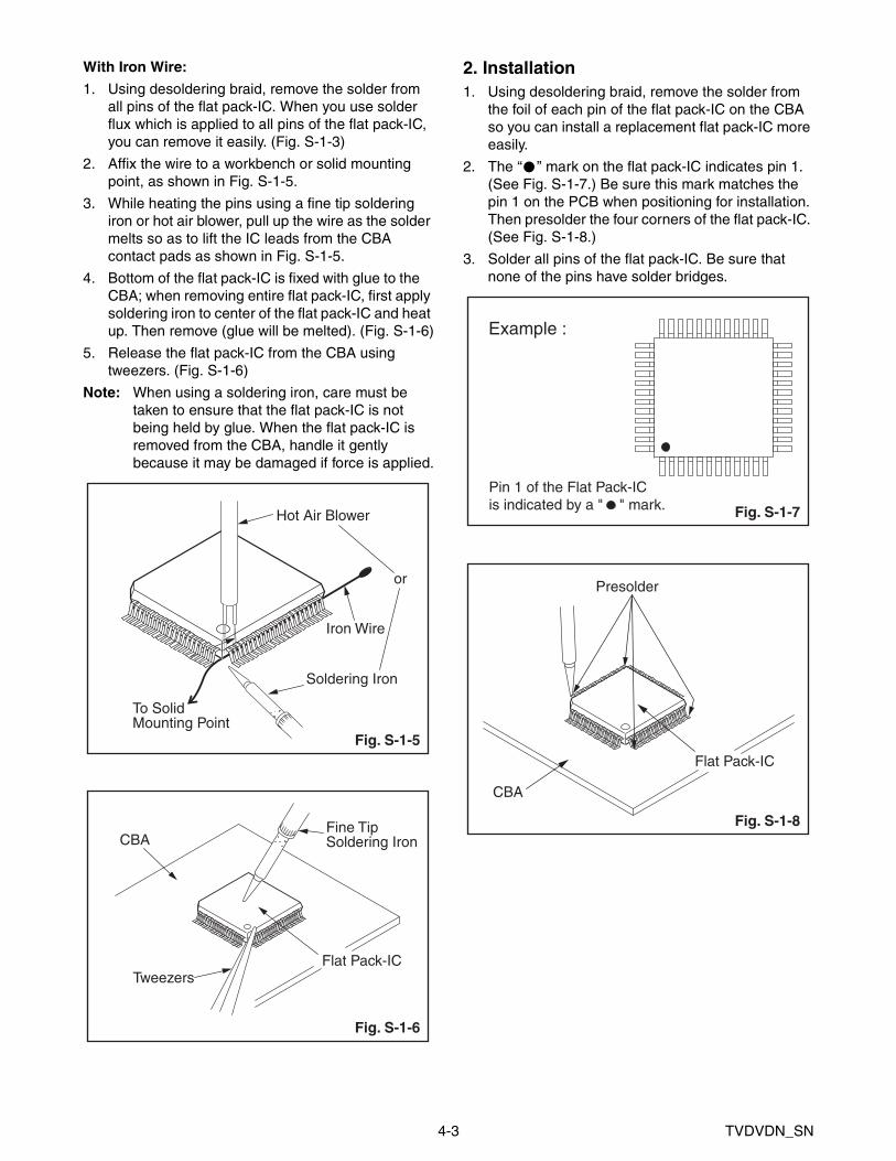
With Iron Wire:
1. Using desoldering braid, remove the solder from all pins of the flat pack-IC. When you use solder flux which is applied to all pins of the flat pack-IC, you can remove it easily. (Fig. S-1-3)
2. Affix the wire to a workbench or solid mounting point, as shown in Fig. S-1-5.
3. While heating the pins using a fine tip soldering iron or hot air blower, pull up the wire as the solder melts so as to lift the IC leads from the CBA contact pads as shown in Fig. S-1-5.
4. Bottom of the flat pack-IC is fixed with glue to the CBA; when removing entire flat pack-IC, first apply soldering iron to center of the flat pack-IC and heat up. Then remove (glue will be melted). (Fig. S-1-6)
5. Release the flat pack-IC from the CBA using tweezers. (Fig. S-1-6)
Note: When using a soldering iron, care must be taken to ensure that the flat pack-IC is not being held by glue. When the flat pack-IC is removed from the CBA, handle it gently because it may be damaged if force is applied.
2. Installation1. Using desoldering braid, remove the solder from
the foil of each pin of the flat pack-IC on the CBA so you can install a replacement flat pack-IC more easily.
2. The “ I ” mark on the flat pack-IC indicates pin 1. (See Fig. S-1-7.) Be sure this mark matches the pin 1 on the PCB when positioning for installation. Then presolder the four corners of the flat pack-IC. (See Fig. S-1-8.)
3. Solder all pins of the flat pack-IC. Be sure that none of the pins have solder bridges.
To Solid Mounting Point
Soldering Iron
Iron Wire
or
Hot Air Blower
Fig. S-1-5
Fine TipSoldering IronCBA
Flat Pack-ICTweezers
Fig. S-1-6
Example :
Pin 1 of the Flat Pack-ICis indicated by a " " mark. Fig. S-1-7
Presolder
CBA
Flat Pack-IC
Fig. S-1-8
4-4 TVDVDN_SN
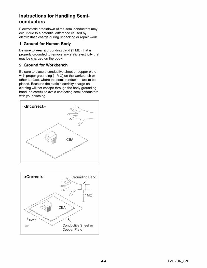
Instructions for Handling Semi-conductorsElectrostatic breakdown of the semi-conductors may occur due to a potential difference caused by electrostatic charge during unpacking or repair work.
1. Ground for Human Body
Be sure to wear a grounding band (1 MΩ) that is properly grounded to remove any static electricity that may be charged on the body.
2. Ground for Workbench
Be sure to place a conductive sheet or copper plate with proper grounding (1 MΩ) on the workbench or other surface, where the semi-conductors are to be placed. Because the static electricity charge on clothing will not escape through the body grounding band, be careful to avoid contacting semi-conductors with your clothing.
<Incorrect>
CBA
Grounding Band
Conductive Sheet orCopper Plate
1MΩ
1MΩ
<Correct>
CBA

5-1 FL11.11-A_DC
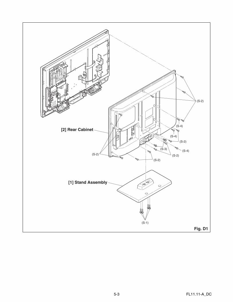
CABINET DISASSEMBLY INSTRUCTIONS
1. Disassembly FlowchartThis flowchart indicates the disassembly steps for the cabinet parts, and the CBA in order to gain access to items to be serviced. When reassembling, follow the steps in reverse order. Bend, route and dress the cables as they were.
2. Disassembly Method*1: Refer to the following "Reference Notes in the
Table."
*2: 32MD311B/F7
Note:
(1) Order of steps in procedure. When reassembling, follow the steps in reverse order. These numbers are also used as the Identification (location) No. of parts in figures.
(2) Parts to be removed or installed.
(3) Fig. No. showing procedure of part location
(4) Identification of parts to be removed, unhooked, unlocked, released, unplugged, unclamped, or desoldered. P = Spring, L = Locking Tab, S = Screw, H = Hex Screw, CN = Connectore.g. 2(S-2) = two Screws of (S-2), 2(L-2) = two Locking Tabs of (L-2)
(5) Refer to the following "Reference Notes in the Table."
Step/Loc. No.
Part Fig. No. Removal Note
[1] Stand Assembly D1 4(S-1) ---
[2] Rear Cabinet D1 13(S-2), 2(S-3), 3(S-4) ---
[3] DVD Holder D2D5
4(S-5), 4(S-6), CN901, CN902 ---
[4] DVD Mechanism
D2D5
(S-7a), 2(S-7b)*1, CN201, CN301, CN801
123456
[5] DVD Main CBA Unit
D2D5 --------------- ---
[6] Inverter CBA
D3D5
6(S-8), CN1001, CN1003, CN1050, CN1100, CN1150, CN1200, CN1900
---
[7] Jack CBA D3D5 2(S-9), CL701B ---
[8]Power Supply CBA
D3D5
7(S-10), CN101, CN301, CN302, CN303, CN801, CN802
---
[1] StandAssembly
[4] DVD Mechanism
[5] DVD Main CBA Unit
[2] Rear Cabinet [10] Speaker
[6] Inverter CBA
[7] Jack CBA
[3] DVD Holder[9] Digital MainCBA Unit
[8] Power SupplyCBA
[13] LCD ModuleAssembly
[14] FrontCabinet
[11] IR SensorCBA
[12] FunctionCBA
[9] Digital Main CBA Unit
D3D5
3(S-11), 8(S-12), CN3005, Shield Box, Jack Holder
---
[10] Speaker D4 8(S-13), Hook, Speaker Holder(L, R) ---
[11] IR Sensor CBA
D4D5 2(S-14), CL103C ---
[12] Function CBA
D4D5
3(S-15),LED Lens*2, Function Knob*2, Shield Plate*2
---
[13]LCD Module Assembly
D4 (S-16) ---
[14] Front Cabinet D4 --------------- ---
↓(1)
↓(2)
↓(3)
↓(4)
↓(5)
Step/Loc. No.
Part Fig. No. Removal Note

5-2 FL11.11-A_DC
Reference Notes1. CAUTION 1: Electrostatic breakdown of the laser
diode in the optical system block may occur as a potential difference caused by electrostatic charge accumulated on cloth, human body etc., during unpacking or repair work.To avoid damage of pickup follow next procedures.
1) Short-circuit the three short lands of FPC cable with solder before removing the FFC cable (CN201). If you disconnect the FFC cable (CN201) before short-circuiting the three short lands of FPC cable, the laser diode of pickup will be destroyed. (Fig. D2)
2) Disconnect the connectors (CN301 and CN801). Remove the screw (S-7a) and remove the DVD Main CBA Unit. (Fig. D2)
2. Reassembly Notes of New DVD Mechanism:
a. To remove the Chassis Cover, remove the two screws (S-7b) as shown in Fig. D2.
b. To avoid damaging the pickup unit (laser diode), confirm that the three short lands (either of two places) are short-circuited by soldering as shown in Fig. D2.
c. Connect the FFC cables of the new DVD Mechanism to the three connectors (CN201, CN301, CN801) on the DVD Main CBA Unit.
d. After confirming that the FFC cables are securely connected to the three connectors, remove the solder from the three short lands. If the solder is not removed, the laser diode will not light and it will not be possible to read discs.
e. Insert the Pin on the Chassis Cover into the Hole on the Main Chassis as shown in Fig. D2. Then tighten the two screws (S-7b) to install the Chassis Cover.
3. CAUTION 2: When reassembling, confirm the FFC cable (CN201) is connected completely. Then remove the solder from the three short lands of FPC cable. (Fig. D2)
4. How to eject a disc in emergencyPress and hold [EJECT] on the unit for more than 5 seconds.
5. How to eject manually 1
1) Remove the Rear Cabinet.
2) Rotate the gear in the direction of the arrow as shown below.
6. How to eject manually 2
1) Remove the Rear Cabinet.
2) To remove the DVD Main CBA Unit, remove the screw (S-7a) in Fig. D2. Do not disconnect connectors.
3) To remove the Chassis Cover, remove the two screws (S-7b) as shown in Fig. D2.
4) Remove a disc.
The gear is turned to the directionof the arrow.
View from the "B" angle
B
5-3 FL11.11-A_DC
[2] Rear Cabinet
(S-1)
[1] Stand Assembly
(S-2)
(S-2)
(S-2)
(S-3)
(S-2)
(S-2)
(S-4)
(S-4)
(S-4)
Fig. D1

5-4 FL11.11-A_DC
Either of two places
FPC Cable
Chassis Cover
A
Main Chassis
Remove the two screws (S-7b), then short-circuit the three short lands by soldering as shown in View from the "A" angle.
View from the "A" angle
Pin
Hole
(S-7b)
(S-5)
(S-7a)
(S-6)
A
[5] DVD Main CBA Unit
[4] DVD Mechanism
[3] DVD Holder
Fig. D2

5-5 FL11.11-A_DC
(S-8)
(S-8)
[7] Jack CBA
Jack Holder
[8] Power Supply CBA[9] Digital Main CBA Unit
[6] Inverter CBA
(S-9)
(S-10)
(S-11) (S-12)
(S-12)
Shield Box
(S-11)
(S-12)
(S-10)
(S-10)
Fig. D3

5-6 FL11.11-A_DC
(S-15)
(S-14)(S-13)Hook
(S-16)
[13] LCD Module Assembly
[11] IR Sensor CBA
[12] Function CBA
Speaker Holder (R)
Speaker Holder (L)
[10] Speaker
[14] Front Cabinet
(S-13)Hook
[10] Speaker
Shield Plate
LED Lens
Function Knob
(S-15)
(S-14)
(S-14)
(S-13)
Hook [11] IR Sensor CBA
[12] Function CBA
Speaker Holder (R)
Speaker Holder (L)
[10] Speaker
[14] Front Cabinet
(S-13)
Hook
[10] Speaker
Fig. D4
[LD320SS2, 32MD301B/F77]
[32MD311B/F7]

5-7 FL11.11-A_DC
TV Cable Wiring Diagram
AC CORD
CN601
CN301CN201
CN801CN401
CL701B
CN902
CN901
CL701A
CN303
CN301CN101 CN802 CN801
CN602
CN201CN1001
CN1900CN1200
CN1150
CN1100
CN1050
CN1003
CN302
To DVD Mechanism
DVD MainCBA Unit
Jack CBA
To Speaker To Speaker
CN3002
CN3003
CN3006
CN3005
CL103C
CL101B
CL103B
Power Supply CBA
Inverter CBA
Function CBAIR Sensor CBA
Digital MainCBA Unit
To LCD ModuleAssembly
To LCD ModuleAssembly
To LCD ModuleAssembly
Fig. D5

6-1 FL11.11EA
ELECTRICAL ADJUSTMENT INSTRUCTIONS
General Note: “CBA” is abbreviation for “Circuit Board Assembly.”Note: Electrical adjustments are required after
replacing circuit components and certain mechanical parts. It is important to perform these adjustments only after all repairs and replacements have been completed. Also, do not attempt these adjustments unless the proper equipment is available.
Test Equipment Required1. NTSC Pattern Generator (Color Bar W/White
Window, Red Color, Dot Pattern, Gray Scale, Monoscope, Multi-Burst)
2. Remote control unit
3. Color Analyzer
How to set up the service mode:
Service mode:1. Turn the power on.
2. Press [MENU] button to display Setup menu.
3. Select “Features”.
4. Select “Current Software Info”.
5. Press [0], [4], [2], [5], [7], [4] and [INFO] buttons on the remote control unit in this order. The following screen appears.
Code : Pic code : MIPS :
Press "POWER" key to exit.
*******-***-*-*****-**** **-*******-*****-**Push 0key
Tuner : Safety :
****-*****-****safety_Non
"*" differs depending on the models.

6-2 FL11.11EA
1. Purity Check ModeThis mode cycles through full-screen displays of red, green, blue, and white to check for non-active pixels.
1. Enter the Service mode.
2. Each time the [7] button on the remote control unit is pressed, the display changes as follows.
3. To cancel or to exit from the Purity Check Mode, press [CH RETURN] or [PREV CH] button.
2. VCOM Adjustment
1. Operate the unit for more than 60 minutes.
2. Set the color analyzer at the zero point calibration and bring the optical receptor pointing at the center of the LCD-Panel at a distance of 1.18 inches(3cm) away from the LCD-Panel surface.Note: The optical receptor must be set perpendicularly to the LCD Panel surface.
3. Enter the Service mode.
4. Press [3] button on the remote control unit.
5. Press [CHANNEL UP/DOWN] buttons on the remote control unit so that the color analyzer value becomes minimum.
6. To cancel or to exit from the VCOM Adjustment, press [CH RETURN] or [PREV CH] button.
[7] button
Note:When entering this mode, the default setting is White mode.
Purity Check Mode
[7] button
Red mode
Green mode
Blue mode
Black mode
[7] button
White mode
[7] button
[7] button
White 20% mode[7] button
Test Point Adj. Point
Screen [CHANNEL UP/DOWN ] buttons
M. EQ. Spec.
Color analyzer See below
Figure
Color Analyzer
To avoid interference from ambient light, this adjustment should be performed in a dark room.
L = 1.18 inches
Perpendicularity

6-3 FL11.11EA
The White Balance Adjustment should be performed when replacing the LCD Panel or Digital Main CBA.
3. White Balance AdjustmentPurpose: To mix red and blue beams correctly for pure white.
Symptom of Misadjustment: White becomes bluish or reddish.
1. Operate the unit for more than 60 minutes.
2. Input the White Raster(70%=70IRE, 40%=40IRE).
3. Set the color analyzer at the CHROMA mode and zero point calibration. Bring the optical receptor pointing at the center of the LCD-Panel at a distance of 1.18 inches(3cm) away from the LCD-Panel surface.Note: The optical receptor must be set perpendicularly to the LCD Panel surface.
4. Enter the Service mode. Press [VOLUME DOWN] button on the remote control unit and select “C/D” mode.
5. [CUTOFF]Press [1] button to select “COR” for Red Cutoff adjustment. Press [3] button to select “COB” for Blue Cutoff adjustment.[DRIVE]Press [4] button to select “DR” for Red Drive adjustment. Press [6] button to select “DB” for Blue Drive adjustment.
6. In each color mode, press [CHANNEL UP/DOWN] buttons to adjust the values of color.
7. Adjust Cutoff and Drive so that the color temperature becomes 12000°K (x= 0.272 / y= 0.278 ±0.005).
8. To cancel or to exit from the White Balance Adjustment, press [CH RETURN] or [PREV CH] button.
Test Point Adj. Point Mode Input
Screen[VOLUME DOWN]button
[VIDEO1]C/D
White Raster (APL 70%)
or(APL 40%)
M. EQ. Spec.
Pattern Generator, Color analyzer
x= 0.272 ± 0.005y= 0.278 ± 0.005
Figure
Color Analyzer
Perpendicularity
INPUT: WHITE 70%, 40%
To avoid interference from ambient light, this adjustment should be performed in a dark room.
L = 1.18 inches
40%=40IRE 70%=70IRE100IRE100IRE
0IRE 0IRE
INPUT SIGNAL
LowLight
HightLight

7-1 FL11.11INT
HOW TO INITIALIZE THE LCD TV/DVD
The purpose of initialization is to place the set in a new out of box condition. The customer will be prompted to select a language and program channels after the set has been initialized.To put the program back at the factory-default, initialize the LCD TV/DVD using the following procedure.
< DVD Section >1. Turn the power on.
2. To enter the service mode, press the service button on the service remote control unit.
- To cancel the service mode, press [POWER] button on the service remote control unit.
3. To put the LCD TV/DVD into the DVD mode, press [CH RETURN] or [PREV CH] on the remote control unit.
4. To put the LCD TV/DVD into the Flash clear mode, press [INPUT SELECT] or [SOURCE] buttons on the remote control unit within five seconds.The following screen appears.
When “OK” appears on the screen, the factory default will be set.
5. To exit this mode, press[CHANNEL UP/DOWN] button to go to TV mode, or press [POWER] button to turn the power off.
Note: The name of buttons may vary with the brand of unit.
< LCD TV Section >1. Turn the power on.
2. Enter the service mode.
- To cancel the service mode, press [POWER] button on the remote control unit.
3. Press [INFO] button on the remote control unit to initialize the LCD television.
4. “INITIALIZED” will appear in the upper right of the screen. “INITIALIZED” color will change to green from red when initializing is completed.
Flash Memory Clear : OK
CHUCKING ON

8-1 FL11.11FW
FIRMWARE RENEWAL MODE
< DVD Section >1. Turn the power on and press [EJECT] button on
the remote control unit to put the LCD TV/DVD into DVD mode. Then remove the disc.
2. To put the LCD TV/DVD into F/W version up mode, press [9], [8], [7], [6], and [MODE] buttons on the remote control unit in this order.Fig. a appears on the screen.
Fig. a Version Up Mode Screen
3. Insert the disc for version up into the disc slot.
4. The LCD TV/DVD enters the F/W version up mode automatically. Fig. b appears on the screen. Make sure to insert the proper F/W for the state of this model.
Fig. b Programing Mode Screen
The appearance shown in (*1) of Fig. b is described as follows:
5. After programming is finished, the disc will be ejected automatically. Fig. c appears on the screen and the checksum will be shown in (*2).
Fig. c Completed Program Mode ScreenAt this time, no button is available.
6. Remove the disc.
7. Unplug the AC cord from the AC outlet then plug in again.
8. Press [EJECT] button on the remote control unit to put the LCD TV/DVD into DVD mode again.
9. Press [1], [2], [3], [4], and [INFO] buttons on the remote control unit in this order. Fig. d appears on the screen.
Fig. d10. Press [CLEAR] button on the remote control unit.
Fig. e appears on the screen.
Fig. eWhen “OK” appears on the screen, the factory default will be set. The firmware renewal mode is now complete.
11. To exit this mode, press [CHANNEL UP/DOWN] button to go to TV mode, or press [POWER] button to turn the power off.
F/W Version Up Mode Model No : ******VERSION : *.**
Please insert a DISCfor F/W Version Up.
EXIT: SELECT
"*******" differs depending on the models.
VERSION : ************.***Reading...
F/W Version Up Mode Model No : ******VERSION : *.**
"*******" differ depending on the models.
(*1)
AppearanceNo. State
Reading... Sending files into the memory
Erasing... Erasing previous version data
Programming...
1
2
3 Writing new version data
VERSION : ************.***CompletedSUM : ****
F/W Version Up Mode Model No : ******VERSION : *.**
"*******" differ depending on the models.
(*2)
MODEL : ****** Version : *.** Region : *
EXIT: SELECTEEPROM CLEAR : CLEAR
"*******" differs depending on the models.
MODEL : ****** Version : *.** Region : *
EEPROM CLEAR : OK
EXIT: SELECTEEPROM CLEAR : CLEAR
"*******" differs depending on the models.
8-2 FL11.11FW
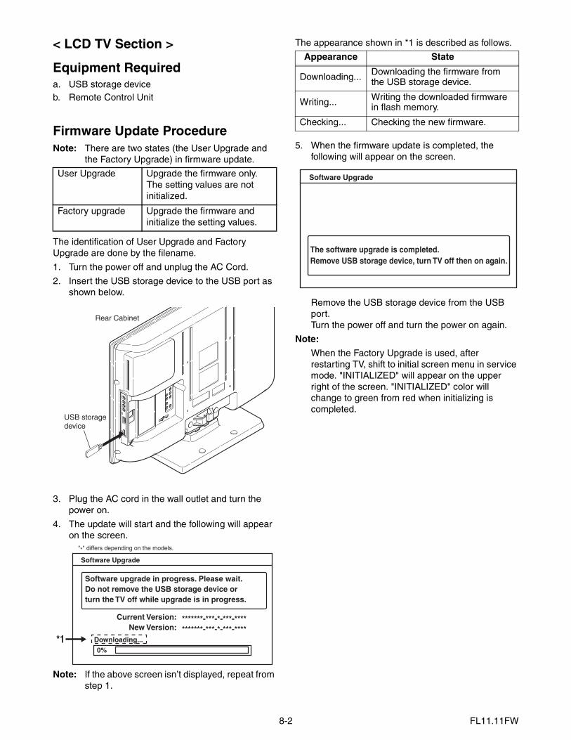
< LCD TV Section >
Equipment Requireda. USB storage deviceb. Remote Control Unit
Firmware Update ProcedureNote: There are two states (the User Upgrade and
the Factory Upgrade) in firmware update.
The identification of User Upgrade and Factory Upgrade are done by the filename.
1. Turn the power off and unplug the AC Cord.
2. Insert the USB storage device to the USB port as shown below.
3. Plug the AC cord in the wall outlet and turn the power on.
4. The update will start and the following will appear on the screen.
Note: If the above screen isn’t displayed, repeat from step 1.
The appearance shown in *1 is described as follows.
5. When the firmware update is completed, the following will appear on the screen.
Remove the USB storage device from the USB port. Turn the power off and turn the power on again.
Note:
When the Factory Upgrade is used, after restarting TV, shift to initial screen menu in service mode. "INITIALIZED" will appear on the upper right of the screen. "INITIALIZED" color will change to green from red when initializing is completed.
User Upgrade Upgrade the firmware only. The setting values are not initialized.
Factory upgrade Upgrade the firmware and initialize the setting values.
USB storagedevice
Rear Cabinet
Software upgrade in progress. Please wait.Do not remove the USB storage device or turn the TV off while upgrade is in progress.
Software Upgrade
Downloading...
Current Version:New Version:
*******-***-*-***-***********-***-*-***-****
0%*1
"*" differs depending on the models.
Appearance State
Downloading... Downloading the firmware from the USB storage device.
Writing... Writing the downloaded firmware in flash memory.
Checking... Checking the new firmware.
Software Upgrade
The software upgrade is completed.Remove USB storage device, turn TV off then on again.

9-1 FL11.11TR
TROUBLESHOOTING
[ Power Supply Section ]
The power cannot be turned on.
The fuse blows out.
FLOW CHART NO.1
FLOW CHART NO.2
Is normal state restored when once unpluggedpower cord is plugged again several seconds?
Check if there is any leak or short-circuiting on theprimary circuit component, and service it if defective.(C605, D601, D602, D603, D604, Q601, Q602, T601)
Yes
No
Yes
Is the fuse (F601) normal? See FLOW CHART No.2 <The fuse blows out.>
No
Yes
Is the AL+33V line voltage normal?No
Check each rectifying circuit of the secondarycircuit and service it if defective.
Check the presence that the primary componentis leaking or shorted and service it if defective.
Check the presence that the rectifying diode or circuit is shorted in each rectifying circuit of secondary side, and service it if defective.
After servicing, replace the fuse.
When the output voltage fluctuates.FLOW CHART NO.3
Does the photocoupler circuit on the secondary side operate normally?
No
Yes
Check IC601, D652, Q631 and their periphery circuit, and service it if defective.
When buzz sound can be heard in the vicinity of power circuit.FLOW CHART NO.4
Check if there is any short-circuit on the rectifying diode and the circuit in each rectifying circuit of the secondary side,and service it if defective. (IC631, Q207, Q209, Q210, Q211, Q501, Q635, Q636, Q637, Q640, Q641, Q642, Q643, D631, D632, D633, D634, D638, D641, D642, D646, D647)
Check D657, R661 and their periphery circuit, and service it if defective.
AL+33V is not output.FLOW CHART NO.5
Is approximately +34V voltage supplied to thecathode of D638?
No
Yes
Check C638, D638, D639 and their periphery circuit, and service it if defective.
Check IC601, D609, D611 and their periphery, circuit and service it if defective.

9-2 FL11.11TR
Check Q207, Q208, D205, P-ON-H1 line and their periphery circuit, and service it if defective.
LCD+24.5V is not output.FLOW CHART NO.6
Is approximately +30V voltage supplied to the collector of Q210?
No
Yes
See FLOW CHART No.5 <AL+33V is not output.>
Replace Q209.
Is approximately +16V voltage supplied to thebase of Q209?
Yes
NoCheck Q207, Q208, D203, D204, D211 and theirperiphery circuit, and service it if defective.
No
LCD+16V is not output.FLOW CHART NO.7
Is approximately +19V voltage supplied to thecollector of Q209?
Yes
Replace Q501.
Is approximately +16V voltage supplied to thebase of Q501?
Yes
NoCheck Q207, Q208, D203, D204, D211 and theirperiphery circuit, and service it if defective.
No
INV+16V is not output.FLOW CHART NO.8
Is approximately +19V voltage supplied to thecollector of Q501?
Yes
Check C631, D631, D635 and their periphery circuit, and service it if defective.
Check C631, D631, D635 and their periphery circuit, and service it if defective.
P-ON+7V is not output.FLOW CHART NO.9
Is approximately +7V voltage supplied to thecollector of D646?
Check C644, D646 and their periphery circuit, and service it if defective.
Yes
No
Check if there is any leak or short-circuit onthe loaded circuit, and service it if defective.

9-3 FL11.11TR
See FLOW CHART No.9 <P-ON+7V is not output.>
See FLOW CHART No.9 <P-ON+7V is not output.>
AL+13V(M+13V) is not output.FLOW CHART NO.12
Yes
NoIs approximately +13V voltage supplied to thecathode of D641 and D642?
Check C639, D642 and their periphery circuit, andservice it if defective.
Check if there is any leak or short-circuit onthe loaded circuit, and service it if defective.
P-ON+5V is not output. (LCD+16V is outputted normally.)FLOW CHART NO.10
Is approximately +6.8V voltage supplied to thecollector of Q643?
Is approximately +6V voltage supplied to the base of Q641 and the base of Q643?
NoYes
Yes
Check D645 and their periphery circuit, and service it if defective.
No
Replace Q641 and Q643.
P-ON+5V(TUNER+5V) is not output. (LCD+16V is outputted normally.)FLOW CHART NO.11
Is approximately +6.7V voltage supplied to thecollector of Q640?
Is approximately +6V voltage supplied to the base of Q641 and the base of Q643(Q640)?
NoYes
Yes
Check D645 and their periphery circuit, and service it if defective.
No
Replace Q641 and Q643(Q640).
D+5.5V is not output.FLOW CHART NO.13
Is approximately +5V voltage supplied to thecathode of D634?
Yes
No
Check if there is any leak or short-circuit onthe loaded circuit, and service it if defective.
Check C634, D634 and their periphery circuit, and service it if defective.

9-4 FL11.11TR
EV+9V is not output.FLOW CHART NO.18
Is approximately +13V voltage supplied to theanode of D909?
P-ON+3.3V is not output.FLOW CHART NO.15
Is approximately +5V voltage supplied to thecathode of D633?
Is the "H" signal (approximately +3.5V) inputted to the base of Q637?
NoYes
Yes
Check C633, D633 and their periphery circuit, andservice it if defective.
Check Q638, Q639, P-ON-H2 line and their periphery circuit, and service it if defective.
Yes
See FLOW CHART No.13 <D+5.5V is not output.>
See FLOW CHART No.14 <P-ON+3V is not output.>
No
No
No
EV+3.3V is not output.FLOW CHART NO.16
Is approximately +4.6V voltage supplied to thecollector of Q903?
Yes
Replace Q637.
Check Q903, D905 and their periphery circuit, and service it if defective.
See FLOW CHART No.13 <D+5.5V is not output.>No
DVD-ON+3.3V is not output.FLOW CHART NO.17
Is approximately +5V voltage supplied to thecollector of Q904?
Yes
Check Q904, D906, and their periphery circuit, and service it if defective.
Check D901, D902, D903, D909 and their periphery circuit, and service it if defective.
P-ON+3V is not output.FLOW CHART NO.14
Is approximately +3V voltage supplied to thecathode of D647?
Yes
No
Check if there is any leak or short-circuit onthe loaded circuit, and service it if defective.
Check C645, D647 and their periphery circuit, and service it if defective.

9-5 FL11.11TR
Is approximately +4V voltage supplied to Pin(3) of IC901?
Yes
NoCheck Q901, Q902, DVD-MAIN PWR line and their periphery circuit, and service it if defective.
See FLOW CHART No.13 <D+5.5V is not output.>No
EV+1.2V is not output.FLOW CHART NO.19
Is approximately +5V voltage supplied to theemitter of Q901?
Yes
Replace IC901.
P-ON+9V is not output. (LCD+16V is outputted normally.)FLOW CHART NO.20
Is approximately +13V voltage supplied to thecollector of Q642?
Is approximately +10V voltage supplied to thebase of Q642?
Is approximately +5V voltage supplied to Pin(1) of IC631?
NoYes
Yes
Yes
Check D670 and their periphery circuit, and service it if defective.
NoCheck Q635, D659 and their periphery circuit, andservice it if defective.
See FLOW CHART No.5 <AL+33V is not output.>
See FLOW CHART No.12 <AL+13V(M+13V) is not output.>
No
No
AL+3.3V is not output.FLOW CHART NO.21
Is approximately +34V voltage supplied to thecollector of Q635?
Yes
Replace IC631.
Replace Q642.
Check C632, D632 and their periphery circuit, and service it if defective.
Check Q207, Q208, D205, P-ON-H1 line and their periphery circuit, and service it if defective.
Replace Q211.
Is approximately -8V voltage supplied to thebase of Q211?
Yes
No
No
LCD-6.8V is not output.FLOW CHART NO.22
Is approximately -9V voltage supplied to theAnode of D632?
Yes

9-6 FL11.11TR
[ Video Signal Section ]
No
Is the "L" pulse sent out Pin(1) terminal of remote control receiver (RS102) when the infrared remote control is activated?
Check the line between Pin(1) terminal of remote control receiver(RS102) and Pin(25) of CN301, and service it if defective.
Yes
Is the "L" pulse supplied to Pin(25) of CN301?
Yes
Is 3.3V voltage supplied to Pin(2) terminal of theremote control receiver (RS102)?
No
FLOW CHART NO.2
Operation is possible from the unit.
Check AL+3.3V line and service it if defective.
NoReplace the remote control receiver(RS102) or the remote control unit.
Yes
Replace Digital Main CBA Unit.
When pressing each switches (SW101A, SW103A~SW107A, SW151~SW153) do the voltage of Pin(29) of CN302 and Pin(2) of CN303 decrease?
Yes
The key operation is not functioning.FLOW CHART NO.1
Are the contact point and installation state of the key switches (SW101A, SW103A~SW107A, SW151~SW153) normal?
Re-install the switches (SW101A, SW103A~SW107A, SW151~SW153) correctly or replace the poor switch.
Check the switches (SW101A, SW103A~SW107A, SW151~SW153) and their periphery, and service it if defective.
Yes
Replace Digital Main CBA Unit.
No
No
No operation is possible from the remote control unit.
Picture does not appear normally.(Video input)FLOW CHART NO.3
Are the video signal inputted to Pin(4) of CN302?
Yes
Check the line between Pin(4) of CN302 and JK752, and service it if defective.
No
Replace Digital Main CBA Unit or LCD ModuleAssembly.

9-7 FL11.11TR
Picture does not appear normally.(S-Video input)FLOW CHART NO.5
Are the video signal outputted to the Pin(6, 8) ofCN302?
Check the line between Pin(6, 8) of CN302 and JK751, and service it if defective.
Check the line between Pin(26, 28) of CN302 andPin(10, 11) of TU301, and service it if defective.
Yes
No
No
Picture does not appear normally.(Tuner input)FLOW CHART NO.4
Are the DIF signal inputted to the Pin(26,28) of CN302?
Yes
Replace Digital Main CBA Unit or LCD ModuleAssembly.
Replace Digital Main CBA Unit or LCD ModuleAssembly.
Pin(6): S-VIDEO-CPin(8): S-VIDEO-Y
Picture does not appear normally.(Y/Pb/Pr input)FLOW CHART NO.6
Are the video signal inputted to the Pin(15, 17, 19) of CN302?
Check the line between Pin(15, 17, 19) of CN302 and input terminals(JK731, JK732, JK733), and service it if defective.
Yes
No
Replace Digital Main CBA Unit or LCD ModuleAssembly.
Pin(15): VIDEO-YPin(17): VIDEO-PbPin(19): VIDEO-Pr
Are the video signal inputted to the Pin(1, 3, 5) of CN902?
Replace DVD Main CBA Unit.No
Picture does not appear normally.(DVD PB)FLOW CHART NO.7
Replace Digital Main CBA Unit or LCD ModuleAssembly.
Pin(5) : DVD-YPin(3) : DVD-PbPin(1) : DVD-Pr
Yes

9-8 FL11.11TR
[ Audio Signal Section ]
Check SP801,SP802 and their periphery circuit,and service it if defective.
Are the audio(L/R) signals inputted to the Pin(1, 44)of IC801?
Are the audio(L/R) signals inputted to the Pin(3, 5)of IC871?
Yes
Yes
Audio is not outputted normally.(Audio input)FLOW CHART NO.1
Are the audio(L/R) signals inputted to Pin(2, 15)of IC771?
Check the line between Pin(2, 15) of IC771 andinput terminal(JK753, JK754), and service it if defective.
Yes
No
No
No
Are the audio(L/R) signals outputted to the Pin(1, 2)of CN801 and CN802?
Are the audio(L/R) signals outputted to the audio output terminal?
Check IC801 and their periphery circuit, and service it if defective.
CN801: SP(L) CN802: SP(R)
JK871: AUDIO(L)-OUT JK872: AUDIO(R)-OUT
No
Yes
Are the audio(L/R) signals inputted to each pin of CN301?
Replace Digital Main CBA Unit.
Check the line between Pin(6, 8) of CN301 and Pin(1, 44) of IC801, and service it if defective.
Check the line between Pin(2, 4) of CN301 and Pin(3, 5) of IC871, and service it if defective.
No Check the line between Pin(1, 7) of IC871 and audio output terminal(JK871, JK872), and service it if defective.
Pin(6) :Pin(8) :Pin(2) :Pin(4) :
AMP(L)-OUTAMP(R)-OUTAUDIO(L)-OUTAUDIO(R)-OUT
No
9-9 FL11.11TR
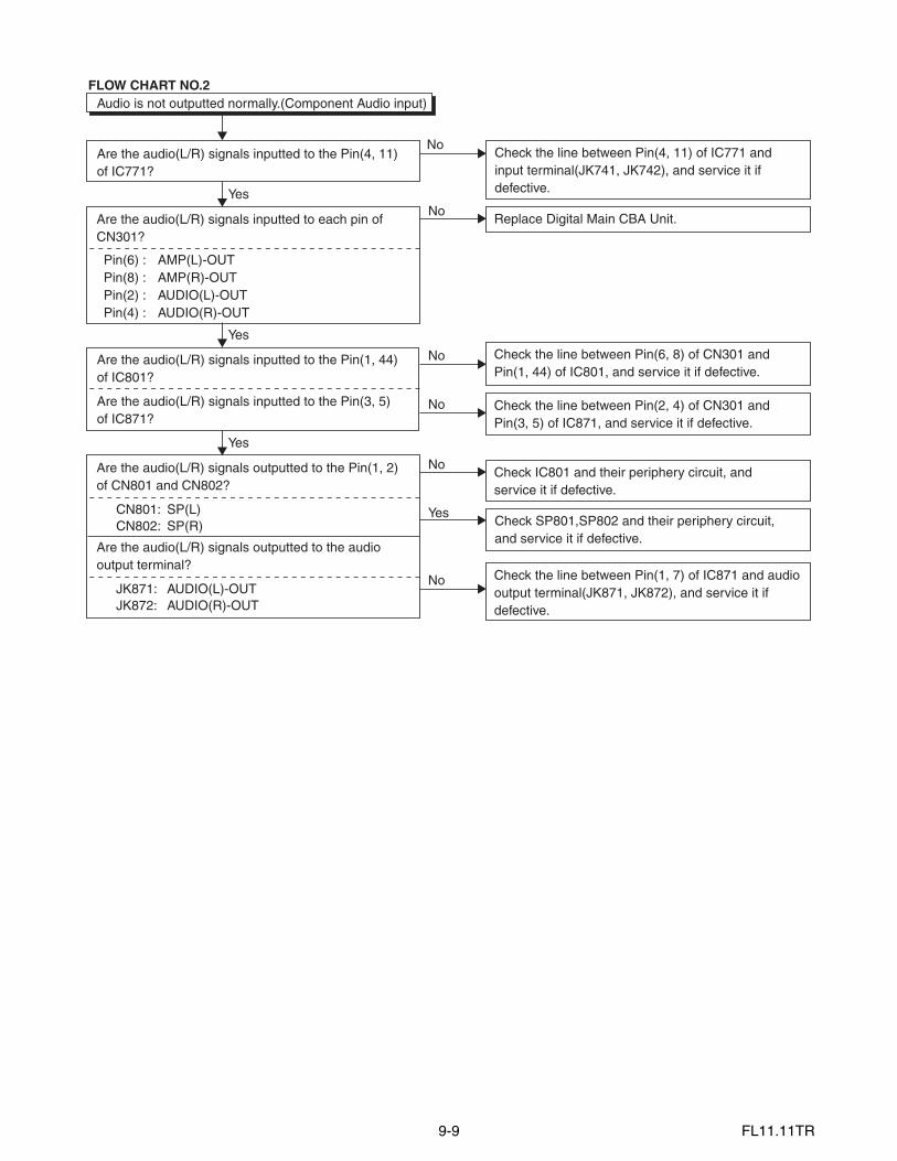
Are the audio(L/R) signals inputted to each pin of CN301?
Replace Digital Main CBA Unit.No
Yes
Audio is not outputted normally.(Component Audio input)FLOW CHART NO.2
Are the audio(L/R) signals inputted to the Pin(4, 11)of IC771?
Check the line between Pin(4, 11) of IC771 andinput terminal(JK741, JK742), and service it if defective.
No
Check SP801,SP802 and their periphery circuit,and service it if defective.
Are the audio(L/R) signals inputted to the Pin(1, 44)of IC801?
Are the audio(L/R) signals inputted to the Pin(3, 5)of IC871?
Yes
Yes
No
No
Are the audio(L/R) signals outputted to the Pin(1, 2)of CN801 and CN802?
Are the audio(L/R) signals outputted to the audio output terminal?
Check IC801 and their periphery circuit, and service it if defective.
CN801: SP(L) CN802: SP(R)
JK871: AUDIO(L)-OUT JK872: AUDIO(R)-OUT
No
Yes
Check the line between Pin(6, 8) of CN301 and Pin(1, 44) of IC801, and service it if defective.
Check the line between Pin(2, 4) of CN301 and Pin(3, 5) of IC871, and service it if defective.
No Check the line between Pin(1, 7) of IC871 and audio output terminal(JK871, JK872), and service it if defective.
Pin(6) :Pin(8) :Pin(2) :Pin(4) :
AMP(L)-OUTAMP(R)-OUTAUDIO(L)-OUTAUDIO(R)-OUT

9-10 FL11.11TR
Yes
Audio is not outputted normally.(Tuner input)FLOW CHART NO.3
Are the DIF signals outputted to the Pin(26, 28)of CN302?
Check TU301 and their periphery circuit, andservice it if defective.
No
Are the audio(L/R) signals inputted to each pin of CN301?
Replace Digital Main CBA Unit.No
Check SP801,SP802 and their periphery circuit,and service it if defective.
Are the audio(L/R) signals inputted to the Pin(1, 44)of IC801?
Are the audio(L/R) signals inputted to the Pin(3, 5)of IC871?
Yes
Yes
No
No
Are the audio(L/R) signals outputted to the Pin(1, 2)of CN801 and CN802?
Are the audio(L/R) signals outputted to the audio output terminal?
Check IC801 and their periphery circuit, and service it if defective.
CN801: SP(L) CN802: SP(R)
JK871: AUDIO(L)-OUT JK872: AUDIO(R)-OUT
No
Yes
Check the line between Pin(6, 8) of CN301 and Pin(1, 44) of IC801, and service it if defective.
Check the line between Pin(2, 4) of CN301 and Pin(3, 5) of IC871, and service it if defective.
No Check the line between Pin(1, 7) of IC871 and audio output terminal(JK871, JK872), and service it if defective.
Pin(6) :Pin(8) :Pin(2) :Pin(4) :
AMP(L)-OUTAMP(R)-OUTAUDIO(L)-OUTAUDIO(R)-OUT

10-1
BLOCK DIAGRAMS1. System Control Block Diagram
FL11.11BLS
KE
Y S
WIT
CH
IR S
EN
SO
R C
BA
FU
NC
TIO
N C
BA
PO
WE
R S
UP
PLY
CB
A
CL1
01B
RE
MO
TE
SE
NS
OR
RS
102
AL+
3.3V
D10
4P
OW
ER
STA
ND
BY
D10
5
D10
6D
VD
LED
14
4
CL1
03B
RE
MO
TE
22
P-O
N-H
15
5
CN
303
CN
302
CN
302
SC
LS
DA
4 5
TU
301
(TU
NE
R U
NIT
)
TO
INV
ER
TE
RB
LOC
K
DIA
GR
AM
(CN
1001
)
TO
PO
WE
R S
UP
PLY
B
LOC
K D
IAG
RA
MP
RO
TE
CT
2P
RO
TE
CT
1
P-O
N-H
2P
-ON
-H1
KE
Y-IN
16
6
CL1
03C
KE
Y S
WIT
CH
KE
Y-IN
13
3K
EY-
IN2
44
CN
201
CN
101
CN
301
Q17
1Q
172
CN
303
CN
401
CN
901
CN
601
CN
902
CN
301
TO
DV
D S
YS
TE
M
CO
NT
RO
L / S
ER
VO
B
LOC
K D
IAG
RA
M
DV
D M
AIN
CB
A U
NIT
KE
Y-IN
27
7D
VD
-LE
D8
8
DV
D-S
CLK
DV
D-C
S
DV
D-S
DAT
A
DV
D-P
-ON
DV
D-R
EM
OT
E
DV
D-D
ISC
-IN
DV
D-D
ISC
-OU
T
DV
D-A
UD
IO-M
UT
E
IC20
1,Q
203,
Q20
4,Q
205
DR
IVE
6P
RO
TE
CT
3
5B
ACK
LIG
HT-
SW
4B
ACK
LIG
HT-
AD
J
14V
CO
M
2626
DV
D-P
-ON
LED
-CO
NT
22
LED
-CO
NT
2525
DV
D-R
EM
OT
E
2424
DV
D-S
DAT
A
2121
DV
D-S
CLK
2222
DV
D-C
S
2323
DV
D-D
ISC
-IN
33
DV
D-D
ISC
-OU
T
1013
DVD-
AUDI
O-M
UTE
DV
D-M
AIN
-PW
R
TO D
VD
DIG
ITA
LS
IGN
AL
PR
OC
ES
SB
LOC
K D
IAG
RA
M
SC
LS
DA
9 8
TU
301
(TU
NE
R U
NIT
)
Eit
her
TU
301
is u
sed
for
Po
wer
Su
pp
ly C
BA
.
* *K
3
IC30
05(M
AIN
MIC
RO
CO
NT
RO
LLE
R)
DIG
ITA
L M
AIN
CB
A U
NIT
CN
3003
CN
3006
CN
3006
XO
UT
25X
IN25
X31
0125
MH
zO
SC
T22
T21
DV
D-S
CLK
U20
U21
N21 M3
M19
DV
D-C
S
T19
V20
W18
PR
OT
EC
T3
H22
VC
OM
-PW
MAB
21
PR
OT
EC
T2
G22
PR
OT
EC
T1
H21
KE
Y-IN
1G
21
DV
D-L
ED
L20
KE
Y-IN
2G
20
BA
CK
LIG
HT-
SW
W20
LED
1K
19
K1
L4
P-O
N-H
2K
20
RE
MO
TE
K21
P-O
N-H
1Y
22
Q30
33
CN
3002
W17
BA
CK
LIG
HT-
AD
J
IC30
06 (
ME
MO
RY
)
SC
K SI
SO
V19
Y21
AA22
Y20
6 5 2 1AA
213
K2
SC
L
SD
A
CN
3003
CN
3002
CS
WP
SC
KS
INS
OU
TC
SW
P
DV
D-S
DAT
A
L21
LED
-CO
NT
DV
D-P
-ON
DV
D-R
EM
OT
E
DV
D-D
ISC
-IN
DV
D-D
ISC
-OU
TD
VD
-AU
DIO
-MU
TE
BU
FF
ER
66
DV
D-P
-ON
1616
LED
-CO
NT
77
DV
D-R
EM
OT
E
88
DV
D-S
DAT
A
1313
DV
D-S
CLK
1111
DV
D-C
S
99
DV
D-D
ISC
-IN
1515
DV
D-D
ISC
-OU
T
2525
DVD-
AUDI
O-M
UTE
U19
DV
D-M
AIN
-PW
R5
5D
VD
-MA
IN-P
WR
2222
SC
L
2121
SD
A
1111
PR
OT
EC
T1
1515
PR
OT
EC
T2
55
PR
OT
EC
T3
2929
VC
OM
-PW
M
2626
BAC
KLI
GH
T-S
W
2828
BAC
KLI
GH
T-A
DJ
KE
Y-IN
129
29
P-O
N-H
19
9
RE
MO
TE
2525
LED
127
27P
-ON
-H2
11
KE
Y-IN
22
2D
VD
-LE
D3
3
TO A
UD
IOB
LOC
K
DIA
GR
AM
AU
DIO
-MU
TE
INP
UT
0IN
PU
T1
Y17
W22
C7-
SP
D-E
ND
VD
-SP
D-E
N
AU
DIO
-MU
TE
INP
UT
0IN
PU
T1
C7-
SP
D-E
ND
VD
-SP
D-E
N
L19
AL+
3.3V
Q30
05
Q30
06

10-2 FL11.11BLV
2. Video Block Diagram
CO
MP
ON
EN
T-Y
-IN
CO
MP
ON
EN
T-P
b-IN
CO
MP
ON
EN
T-P
r-IN
JK73
1
JK73
2
JK73
3
VID
EO
-IN
44
S-V
IDE
O-C
-IN
66
S-V
IDE
O-Y
-IN
88
S-V
IDE
O-S
W5
5C
OM
-VID
EO-Y
-IN15
15CO
M-V
IDEO
-Pb-
IN17
17CO
M-V
IDEO
-Pr-I
N19
19
JAC
K C
BA
CL7
01A
C
L701
BV
IDE
O-I
N5
S-V
IDE
O-C
-IN
3S
-VID
EO
-Y-I
N1
5 3 1JK
751
S-V
IDE
O-I
N
CY
JK75
2V
IDE
O-I
N
S-V
IDE
O-S
W-IN
22
PO
WE
R S
UP
PLY
CB
A
TU
301
DIF
-OU
T1
11D
IF-O
UT
210
(TU
NE
R U
NIT
) IF-A
GC
9
TU
301
DIF
-OU
T1
13D
IF-O
UT
212
(TU
NE
R U
NIT
) IF-A
GC
14
CN
302
DIF
-OU
T1
2626
IF-A
GC
2424
DIF
-OU
T2
2828
CN
302
CN
902
CN
303 20
20D
VD
-Pb
2222
DV
D-Y
1818
DV
D-P
r
WF
1W
F2
WF
3
WF
9
WF
4W
F5
WF
6
WF
8
WF
10
VID
EO
SIG
NA
LA
UD
IO S
IGN
AL
* *
Eit
her
TU
301
is u
sed
for
Po
wer
Su
pp
ly C
BA
.
DIG
ITA
L M
AIN
CB
A U
NIT
TO D
VD
DIG
ITA
LS
IGN
AL
PR
OC
ES
SB
LOC
K D
IAG
RA
M
DIF
-OU
T1
DIF
-OU
T2
IF-A
GC
VID
EO
-IN
S-V
IDE
O-C
-IN
S-V
IDE
O-Y
-IN
S-V
IDE
O-S
WC
OM
-VID
EO-Y
-IN
COM
-VID
EO-P
r-IN
COM
-VID
EO-P
b-IN
CN
601
DV
D M
AIN
CB
A U
NIT
DV
D-P
bD
VD
-Y3
6D
VD
-Pb
DV
D-P
r1
4D
VD
-Pr
58
DV
D-Y
DV
D-P
bD
VD
-Pr
DV
D-Y
TO D
IGIT
AL
SIG
NA
L P
RO
CE
SS
BLO
CK
DIA
GR
AM
CN
3006
CN
3006
CN
3003

10-3
3. Audio Block Diagram
FL11.11BLA
IC77
1(A
UD
IO S
ELE
CTO
R)
AU
DIO
(L)-
OU
T
AU
DIO
(R)-
OU
T
HD
MI-
AU
DIO
(L)-
IN
HD
MI-
AU
DIO
(R)-
IN
JK72
1
JK72
2
JK87
1
JK87
2
CO
MP
ON
EN
T-A
UD
IO(L
)-IN
CO
MP
ON
EN
T-A
UD
IO(R
)-IN
JK74
1
JK74
2
2 4 1 5 15 11 12 14
JAC
K C
BA
CL7
01A
CL7
01B
AU
DIO
(L)-
IN7
7A
UD
IO(R
)-IN
99
AU
DIO
(L)
-IN
AU
DIO
(R)
-IN
JK75
3
JK75
4
CN
302
AU
DIO
(L)
1313
AU
DIO
(R)
1111
CN
302
INP
UT
110
10IN
PU
T0
1212 C
N30
02C
N30
1A
UD
IO(L
)-O
UT
22
AU
DIO
(R)-
OU
T4
4A
MP
(L)-
OU
T6
6A
MP
(R)-
OU
T8
8
PO
WE
R S
UP
PLY
CB
AD
IGIT
AL
MA
IN C
BA
UN
IT
20
IC80
1 (A
UD
IO A
MP
)
1 44
9,10
13,1
4
35,3
631
,32
MU
TE
CO
NT
RO
L
CN
801
CL8
01S
P80
1S
PE
AK
ER
L-C
H
CN
802
SP
(R)-
1
CL8
02S
P80
2S
PE
AK
ER
R-C
H
PW
M1
PW
M2
DR
IVE
1
CN
302
CN
3006
CN
303
CN
3003
AU
DIO
-MU
TE
2020
JK84
1D
IGIT
AL
AU
DIO
-OU
T(C
OA
XIA
L)Q
841
Q77
1
Q77
2
BU
FF
ER
Q87
1
Q87
3,Q
874
MU
TE
Q87
2 MU
TE
SP
DIF
22
DV
D-S
PD
IF28
28
SP
(R)+
2
SP
(L)-
1S
P(L
)+2
Q80
1
CO
NT
RO
L LO
GIC
3
109
13
IC87
1 (O
P A
MP
)
13
75
DR
IVE
2
DR
IVE
CN
601
CN
902
DV
D-A
UD
IO(L
)9
12D
VD
-AU
DIO
(R)
1114
DV
D-S
PD
IF13
16
IC95
1 (O
P A
MP
)
13
75
IC30
10(D
/A C
ON
VE
RT
ER
)
D/A
CO
NV
ER
TE
R15 14
8 7 6 5
(L-C
H)
(R-C
H)
AU
DIO
(L)
AU
DIO
(R)
CN
303
DV
D-A
UD
IO(L
)24
24D
VD
-AU
DIO
(R)
2626
DV
D-A
UD
IO(L
)D
VD
-AU
DIO
(R)
TO
DIG
ITA
LS
IGN
AL
PR
OC
ES
SB
LOC
KD
IAG
RA
M
TO
DIG
ITA
LS
IGN
AL
PR
OC
ES
SB
LOC
KD
IAG
RA
M
INP
UT
1
DV
D-A
UD
IO(L
)D
VD
-AU
DIO
(R)
DV
D-S
PD
IF
LRC
LKB
CLK
AD
ATA
1A
CLK
INP
UT
0A
UD
IO-M
UT
E
TO
SY
ST
EM
CO
NT
RO
LB
LOC
KD
IAG
RA
M
TO
SY
ST
EM
CO
NT
RO
LB
LOC
KD
IAG
RA
M
4
1
2
4
1
2
AU
DIO
SIG
NA
L
TO D
VD
D
IGIT
AL
SIG
NA
L
PR
OC
ES
SB
LOC
K
DIA
GR
AM
DV
D M
AIN
CB
A U
NIT
WF
11 WF
13
WF
12
DV
D-S
PD
-EN
WF
7C
N30
06
CN
3006
CN
3003
C7-
SP
DIF
IC30
16
(BU
FF
ER
GAT
E)
IC30
17
(BU
FF
ER
GAT
E)
C7-
SP
D-E
N
IC30
15
(OP
AM
P)
1
67
2A
MP
(R)-
OU
T
AM
P(L
)-O
UT
10-4
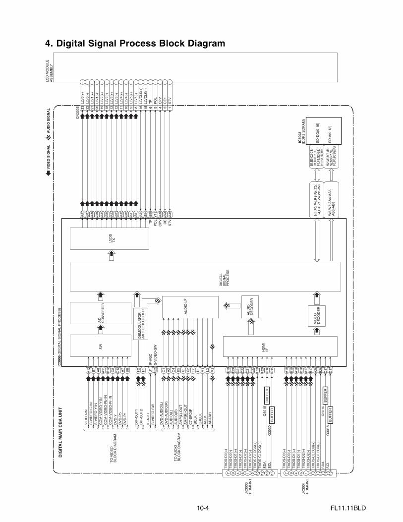
4. Digital Signal Process Block Diagram
FL11.11BLD
DIG
ITA
L M
AIN
CB
A U
NIT
IC30
05 (
DIG
ITA
L S
IGN
AL
PR
OC
ES
S)
CN
3005
LLV
1(+
)21
LLV
1(-)
20
LLV
0(+
)23
LLV
0(-)
22
LLV
2(+
)19
LLV
2(-)
18LL
V3(
+)
13LL
V3(
-)12
LLV
4(+
)11
LLV
4(-)
10LL
V5(
+)
9LL
V5(
-)8
LLV
CLK
(+)
16LL
VC
LK(-
)15
TP
6P
OL
5C
PV
4O
E1
3S
TV
1
LVD
ST
X
DIG
ITA
LS
IGN
AL
PR
OC
ES
S
A/D
CO
NV
ER
TER
S-V
IDE
O-Y
-IN
SW
B12 D8
A11
S-V
IDE
O-C
-IN
A8
VID
EO
-IN
B7
CO
M-V
IDE
O-P
r-IN
CO
M-V
IDE
O-P
b-IN
CO
M-V
IDE
O-Y
-IN
A7
B8
C12
DV
D-P
rD
VD
-Pb
DV
D-Y
A12
IF-A
GC
HD
MI-
IN1
HD
MI-
IN2
JK30
03
TM
DS
-D0(
+)
TM
DS
-D0(
-)T
MD
S-D
1(+
)T
MD
S-D
1(-)
TM
DS
-D2(
+)
TM
DS
-D2(
-)
SD
AS
CL
7 9 4 6 1 3 10 12 16 15 7 9 4 6 1 3 10 12 16 15
JK30
04
TM
DS
-D0(
+)
TM
DS
-D0(
-)T
MD
S-D
1(+
)T
MD
S-D
1(-)
TM
DS
-D2(
+)
TM
DS
-D2(
-)T
MD
S-C
LOC
K(+
)T
MD
S-C
LOC
K(-
)S
DA
SC
L
TM
DS
-CLO
CK
(+)
TM
DS
-CLO
CK
(-)
DE
MO
DU
LATO
R/M
PE
G D
EC
OD
ER
AU
DIO
I/F
TO A
UD
IOB
LOC
K D
IAG
RA
MA
MP
(L)-
OU
TA
MP
(R)-
OU
T
C7-
SP
DIF
G1
G2 L2
B1,B
9,C2
,C8,
D1,D
3,D7
,D9,
F1,F
9,G
2,G
8,H1
,H3,
H7,H
9
M2,
M3,
M7,
M8,
N2,N
3,N7
,N8,
P2,P
3,P7
,P8,
R2
(DD
R2
SD
RA
M)
HD
MI
I/F
AU
DIO
DE
CO
DE
R
DIF
-OU
T1
DIF
-OU
T2
IF-A
GC
TO V
IDE
OB
LOC
K D
IAG
RA
M
VID
EO
DE
CO
DE
R
S-V
IDE
O-S
WS
-VID
EO
-SW
B5
AU
DIO
(R)
C4
AU
DIO
(L)
A2
DV
D-A
UD
IO(R
)C
1D
VD
-AU
DIO
(L)
VID
EO
SIG
NA
LA
UD
IO S
IGN
AL
LCD
MO
DU
LEA
SS
EM
BLY
Q30
16B
UF
FE
RB
UF
FE
RQ
3018
A18
A19
B19
B18
A17
B17
A20
B20
C17
D17
D21
E19
E20
D22
C21
C22
F19
F20
D16
Q30
15B
UF
FE
RB
UF
FE
RQ
3020
D15F2 J1F1
AB22
SD
-DQ
(0-1
5)
SD
-A(0
-12)
IC30
02
N4,
P2,
P4,
R1-
R4,
T2,
T4,
U4,
V1,
V4,
W1-
W3
W5,
W7,
AA
4-A
A8,
AB
3-A
B8
AA17
AB17
AA16
AB16
AA15
AB15
AA13
AA12
AA11
AB11
AB12
AB13
AA14
AB14
AB19
Y
19AA
18AB
20AA
19
TP
PO
LC
PV
OE
ST
V
AC
LKA
DAT
A1
BC
LKLR
CLK
M2
L1 M1
L3

10-5
5. Inverter Block Diagram
FL11.11BLINV
INV
ER
TE
R C
BA
CN
1001
P
RO
TE
CT
310
BAC
KLI
GH
T-A
DJ
12V
CO
M2
BA
CK
LIG
HT-
SW
11T
O S
YS
TE
MC
ON
TR
OL
BLO
CK
D
IAG
RA
M(C
N20
1)
T19
50
10 11 14 15
2 3 4 5 7 8
14 3
2 Q19
70
Q19
71IC19
30
14 3
2
IC19
31
Q19
31
TO
PO
WE
RS
UP
PLY
B
LOC
K
DIA
GR
AM
(CN
602)
HO
T
CO
LD
HO
T C
IRC
UIT
. BE
CA
RE
FU
L.
Q19
72
SW
ITC
HIN
GQ
1930
CN
1900
Q19
32
IC10
00
(PW
M C
ON
TR
OL)
BA
CK
LIG
HT
1 2 1 2 1 2
CN
1100
CN
1150
CN
1200
BA
CK
LIG
HT
BA
CK
LIG
HT
T11
00
Q15
51,
Q15
52,
Q15
53
Q10
01
Q10
03
Q12
10
Q12
11
Q11
60
Q11
61
Q11
10
Q11
11
Q15
00
Q18
01,Q
1802
, Q
1803
,Q18
04Q
1800
,Q18
15 Q10
04,
Q10
05
Q15
50T
1150
4 1 3
78 6 5
2 T12
00
DR
IVE
Q15
01,
Q15
02,
Q15
03
DR
IVE
OS
C
PWM
CO
NTR
OL
LOG
IC
VC
C
DC
T
CU
RR
ENT
CO
NTR
OL
SWIT
CH
CU
RR
ENT
CO
NTR
OL
SWIT
CH
OV
ER
VO
LTA
GE
PR
OT
EC
TOR
OV
ER
VO
LTA
GE
PR
OT
EC
TOR
OV
ER
VO
LTA
GE
PR
OT
EC
TOR
OV
ER
VO
LTA
GE
PR
OT
EC
TOR
OV
ER
VO
LTA
GE
PR
OT
EC
TOR
OV
ER
VO
LTA
GE
PR
OT
EC
TOR
Q10
60
OV
ER
VO
LTA
GE
PR
OT
EC
TOR
Q10
61
OV
ER
VO
LTA
GE
PR
OT
EC
TOR
11 8
56
153412 16 2 1
SW
+16
V
SW
SW
+16
V
Q16
00
Q16
21
LC
D M
OD
UL
EA
SS
EM
BLY
T10
50
4 1 3
78 6 5
24 1 3
78 6 5
2 4 1 3
78 6 5
2
BA
CK
LIG
HT
1 2
CN
1050
IC17
00
(CO
MP
AR
AT
OR
) 67
5 2 39 10
18
13 1214
AC
L2
HO
T-G
ND
1
INV
+16
V
10C
N10
03V
CO
M
NO
TE
:T
he v
olta
ge fo
r pa
rts
in h
ot c
ircui
t is
mea
sure
d us
ing
hot G
ND
as
a co
mm
on te
rmin
al.

10-6
6. Power Supply Block Diagram
FL11.11BLP
HO
TC
OL
DP
OW
ER
SU
PP
LY C
BA
HO
T C
IRC
UIT
. BE
CA
RE
FU
L.
Q60
2S
WIT
CH
ING
CO
NT
RO
L
14 3
2
IC60
1
T60
1
TO
INV
ER
TE
RB
LOC
K
DIA
GR
AM
(C
N19
00)
CN
602
3
HO
T-G
ND
1A
CL
2
LIN
EF
ILT
ER
L601
AC
601
AC
CO
RD
BR
IDG
ER
EC
TIF
IER
D60
1- D
604
54
11 14 12 17 18 13 16 15 1997 8
FE
ED
BA
CK
Q60
1S
WIT
CH
ING
Q63
1
CN
201
CN
1001
CN
401
CN
301
Q20
7,Q
208
SW
ITC
HIN
G
Q21
1S
W-8
V
SW
Q40
1
Q20
9,D
204
SW
+16
V
Q90
4,D
906
SW
+3.
3V
Q90
3,D
905
SW
+3.
3V
Q63
5IC
631
+3.
3VR
EG
.2
3
Q63
4
Q63
8,Q
639
Q64
1,64
3S
W+
5V
Q64
0S
W+
5V
Q64
2S
W+
9V
Q50
1S
W+
16V
Q63
7,D
666
SW
+3.
3V
IC90
1+
1.2V
RE
G.
LIN
EF
ILT
ER
L602
4A/1
25V
F60
1 4A
/125
V
P-O
N-H
1TO
SY
ST
EM
C
ON
TR
OL
BLO
CK
DIA
GR
AM
P-O
N-H
2
+5V
RE
G.
PR
OT
EC
T2
DV
D-M
AIN
-PW
R
PR
OT
EC
T1
SW
ITC
HIN
G
AL+
33V
P-O
N+
5V
AL+
3.3V
AL+
13V
TU
NE
R+
5V
P-O
N+
9V
19,2
0
1228,9
21,2
2
13,1
4
LCD
+16
VLC
D-8
V
INV
+16
VV
GH
P-O
N+
3.3V
P-O
N+
3VP
-ON
+7V
AL+
3.3V
P-O
N+
3.3V
P-O
N+
5V
AL+
3.5V
DVD-
ON+
3.3V
EV
+3.
3VD
VD
-ON
+5V
EV
+9V
EV
+1.
2V
INV
ER
TE
R C
BA
DV
D M
AIN
CB
A U
NIT
DIG
ITA
L M
AIN
CB
A U
NIT
13LC
D-8
V13
P-O
N+
3.3V
19,2
0
P-O
N+
3.3V
1210
VG
H10
INV
+16
V2
LCD
+16
V8,
9
AL+
3.3V
21,2
21610
P-O
N+
7V16
P-O
N+
3V10
P-O
N+
5V13
,14
Q21
0Q
201,
Q20
2,Q
212
SW
+24
.5V
Q90
1,Q
902
SW
ITC
HIN
G
1011
,12
6~8
4,59
DV
D-O
N+
5V10
EV
+9V
11,1
2
1A
L+3.
3V1
EV
+3.
3V6~
8
EV
+1.
2V4,
5
DV
D-O
N+
3.3V
9
CN
901
CN
3002
CA
UT
ION
!F
ixed
vol
tage
(or
Aut
o vo
ltage
sel
ecta
ble)
pow
er s
uppl
y ci
rcui
t is
used
in th
is u
nit.
If M
ain
Fus
e (F
601)
is b
low
n , c
heck
to s
ee th
at a
ll co
mpo
nent
s in
the
pow
er s
uppl
yci
rcui
t are
not
def
ectiv
e be
fore
you
con
nect
the
AC
plu
g to
the
AC
pow
er s
uppl
y.O
ther
wis
e it
may
cau
se s
ome
com
pone
nts
in th
e po
wer
sup
ply
circ
uit t
o fa
il.
For
con
tinue
d pr
otec
tion
agai
nst r
isk
of fi
re,
repl
ace
only
with
sam
e ty
pe 4
A, 1
25V
fuse
.C
AU
TIO
N !
:
AT
TE
NT
ION
: U
tilis
er u
n fu
sibl
e de
rec
hang
e de
mêm
e ty
pe d
e 4
A, 1
25V
.4A
/125
V
NO
TE
:T
he v
olta
ge fo
r pa
rts
in h
ot c
ircui
t is
mea
sure
d us
ing
hot G
ND
as
a co
mm
on te
rmin
al.

10-7
7. DVD System Control / Servo Block Diagram
FL11.11BLSD
IC30
1(S
ER
VO
DR
IVE
)
CN
301
M
SLE
D
MO
TO
R
M
SP
IND
LE
MO
TO
R
IC10
1(M
ICR
O C
ON
TR
OLL
ER
)
+ -+ -
+ -+ -
+ -+ - + -
SLE
DM
OTO
RD
RIV
E
FO
CU
SA
CT
UAT
OR
DR
IVE
SP
IND
LEM
OTO
RD
RIV
E
TR
AC
KIN
GA
CT
UAT
OR
DR
IVE
126
LOA
D-D
ISC
SLD
67
SP
DL
66
TR
AC
KIN
GD
RIV
E
127
FO
CU
S D
RIV
EF
S(+
)F
S(-
)
TS
(+)
TS
(-)
LOA
D-D
ISC
1S
P(+
)2
SP
(-)
6LO
AD
-DIS
C3
GN
D4
SL(
-)5
SL(
+)
VR
EF
RE
SE
T70
RE
SE
T
IC46
2
13
+3.
3V
IC20
2(O
P A
MP
)
15 16 14 13 12 11 17 182364 531 225 2427 26
121
SP
-RO
T
124
FD
-OF
ST
123
TD
-OF
ST
RE
SE
T
IC46
1
21
+3.
3V
TO D
VD
DIG
ITA
L S
IGN
AL
PR
OC
ES
S
BLO
CK
DIA
GR
AM
DR
IVE
CB
A
DV
D M
AIN
CB
A U
NIT
122
SL-
AD
S
DIS
C-I
N
12 6
753
3D
VD
-DIS
C-I
N3
2DV
D-DI
SC-O
UT2C
N80
1C
N50
01
DIS
C-O
UT
SE
NS
OR
CB
A
+3.
3V
1LE
D-P
OW
ER
1
Q80
4
63D
VD
-DIS
C-I
N61
DV
D-D
ISC
-OU
T
TO SY
ST
EM
CO
NT
RO
LB
LOC
K D
IAG
RA
M
53D
VD
-SC
LK54
DV
D-C
S
49D
VD
-RE
MO
TE
56D
VD
-SD
ATA
DV
D-S
CLK
DV
D-C
SD
VD
-SD
ATA
DV
D-R
EM
OT
E
LED
-CO
NT
DV
D-D
ISC
-OU
TD
VD
-DIS
C-I
N
77D
VD
-P-O
ND
VD
-P-O
N
65
1
NO
TE
:
Eith
er IC
461
or IC
462
is u
sed
for
DV
D M
AIN
CB
A U
NIT
.

10-8 FL11.11BLDD
C16
D18
A17
B15
DV
D-L
D8
CD
-LD
10
PD
-MO
NI
7
FS
(+)
2F
S(-
)3
TS
(+)
1T
S(-
)4C
N20
1
CN
201
CN
201
IC20
1(S
W)
IC10
1(M
ICR
O C
ON
TR
OLL
ER
)
FS
FS
(+)
CD
/DV
D
FS
(-)
TS
(+)
TS
(-)
TS
DE
TE
CTO
R
CD
/DV
D19
Q25
1,Q
252
CDDV
D
AM
P
Q25
3,Q
254
AM
P
4
13
6
GN
D(C
D-P
D)
5G
ND
(LD
)9
RF
SIG
NA
LP
RO
CE
SS
CIR
CU
IT
DV
D/C
DF
OR
MAT
TE
R
AU
DIO
I/F VID
EO
I/FN
TS
C/P
AL
EN
CO
DE
R
DM
A
BC
U
INS
T.R
OM
32B
ITC
PU
DAT
AR
AM
INT
ER
RU
PT
CO
NT
RO
LLE
RW
ATC
H D
OG
TIM
ER
CP
UI/F
TIM
ER
DE
CO
DE
RI/F
CP
UI/F
RE
AD
ME
MO
RY
DAT
AR
AM
DS
PD
EC
OD
ER
I/O PR
OC
ES
SO
R
INS
T.R
OM
DAT
AR
AM
INS
T.R
OM
SE
RIA
L
D/A
GE
NE
RA
LI/O IN
TE
RR
UP
TC
ON
TR
OLL
ER
TIM
ER
WAT
CH
DO
GT
IME
R
RE
MO
TE
CO
NT
RO
L
32B
IT C
PU
ST
RE
AM
I/F
EX
TE
RN
AL
ME
MO
RY
I/FS
DR
AM
EC
C
UM
AC
100
115
116
113
114
106
104
105
103
62
DE
BU
G
BC
U
INS
TC
AC
HE
DAT
AC
AC
HE
D/A
131
130
Y Pb
DV
D-Y
DV
D-P
b
152
DV
D-S
PD
IF
151
DVD
-AU
DIO
-MU
TE
146
DVD
-AU
DIO
(R)
144
DVD
-AU
DIO
(L)
SD
RA
M A
DD
RE
SS
(0-1
0)
IC10
3(F
LAS
H R
OM
)
FLA
SH
RO
M
29 36 38 45
~ ~
FD
Q (
0-15
)
~
1 9 16 25 48
~
FAD
R (
0-19
)
SD
RA
M D
ATA
(0-1
5)
PIC
KU
P
TO D
VD
SY
ST
EM
C
ON
TR
OL
/ SE
RV
OB
LOC
K D
IAG
RA
M
DV
D M
AIN
CB
A U
NIT
TO V
IDE
OB
LOC
K
DIA
GR
AM
TO A
UD
IOB
LOC
K
DIA
GR
AM
IC50
3(S
DR
AM
)
SD
RA
M D
ATA
(0-1
5)
SD
RA
M A
DD
RE
SS
(0-1
0)19
4
209~
2 13 42 53
~ ~
22 26 29 34
~ ~
159
178~
99 98 97
21~
3034
~42
212
1~4
7~14
17~
1821
5 2
16
AU
DIO
D/A
CO
NV
ER
TE
R
D/A
129
Pr
DV
D-P
r
GN
D(D
VD-P
D)
6
VID
EO
SIG
NA
LA
UD
IO S
IGN
AL
TO
SY
ST
EM
CO
NT
RO
LB
LOC
KD
IAG
RA
M
8. DVD Digital Signal Process Block Diagram

11-1 FL11.11SC
SCHEMATIC DIAGRAMS / CBA AND TEST POINTS
Standard Notes
WARNING
Many electrical and mechanical parts in this chassis have special characteristics. These characteristics often pass unnoticed and the protection afforded by them cannot necessarily be obtained by using replacement components rated for higher voltage, wattage, etc. Replacement parts that have these special safety characteristics are identified in this manual and its supplements; electrical components having such features are identified by the mark “#” in the schematic diagram and the parts list. Before replacing any of these components, read the parts list in this manual carefully. The use of substitute replacement parts that do not have the same safety characteristics as specified in the parts list may create shock, fire, or other hazards.
Notes:1. Do not use the part number shown on these
drawings for ordering. The correct part number is shown in the parts list, and may be slightly different or amended since these drawings were prepared.
2. All resistance values are indicated in ohms (K = 103, M = 106).
3. Resistor wattages are 1/4W or 1/6W unless otherwise specified.
4. All capacitance values are indicated in µF (P = 10-6 µF).
5. All voltages are DC voltages unless otherwise specified.
6. This schematic diagrams are masterized version that should cover the entire FL11.11 chassis models.Thus some parts in detail illustrated on this schematic diagrams may vary depend on the model within the FL11.11 chassis.Please refer to the parts lists for each models.
7. The Circuit Board layout illustrated on this service manual is the latest version for this chassis at the moment of making this service manual. Depend on the mass production date of each model, the actual layout of each Board may differ slightly from this version.

11-2 FL11.11SC
LIST OF CAUTION, NOTES, AND SYMBOLS USED IN THE SCHEMATIC DIAGRAMS ON THE FOLLOWING PAGES:
1. CAUTION:CAUTION: FOR CONTINUED PROTECTION AGAINST RISK OF FIRE, REPLACE ONLY WITH SAME TYPE_A,_V FUSE.
ATTENTION: UTILISER UN FUSIBLE DE RECHANGE DE MÊME TYPE DE_A,_V.
2. CAUTION: Fixed Voltage (or Auto voltage selectable) power supply circuit is used in this unit. If Main Fuse (F601) is blown, first check to see that all components in the power supply circuit are not defective before you connect the AC plug to the AC power supply. Otherwise it may cause some components in the power supply circuit to fail.
3. Note:1. Do not use the part number shown on the drawings for ordering. The correct part number is shown in the
parts list, and may be slightly different or amended since the drawings were prepared.
2. To maintain original function and reliability of repaired units, use only original replacement parts which are listed with their part numbers in the parts list section of the service manual.
4. Voltage indications on the schematics are as shown below: Plug the TV power cord into a standard AC outlet.:
5. How to read converged lines
6. Test Point Information
2 31 5.0< 0 >
TV mode DVD mode
Unit: Volts
5.0
The same voltage forboth TV & DVD modes
Unit: Volts
Indicates that the voltageis not consistent here.
3
2
1
A B C D
1-B1
1-D3
AREA D3
AREA B1
1-D3
Distinction AreaLine Number (1 to 3 digits)
Examples:1. "1-D3" means that line number "1" goes to the line number "1" of the area "D3". 2. "1-B1" means that line number "1" goes to the line number "1" of the area "B1".
: Indicates a test point with a jumper wire across a hole in the PCB.
: Used to indicate a test point with a component lead on foil side.
: Used to indicate a test point with no test pin.
: Used to indicate a test point with a test pin.
The reference number of parts on Schematic Diagrams/CBA can be retrieved by application search function.

11-3
GD
S
TK5A50DQ601
2SC2120-OQ602
4
3 2
1
IC601LTV817MCF
D611
0.027/100V
C609
0.082/100V
C612
470P/2KV
C611
1000P/250VC691
1HOT-GND
CN6022ACL
BEADBC601
OPENC610
D609
1200P/100V
C613
FR154D631
2SD400Q209
C2210.01
D203
SB360BHD646
FR104-BD643
0.1C682
2200P/1KVC637
FR154D638
KTA1267-GR-AT/PQ207
KTC3198-Y-AT/PQ208
2SA950-OQ636
FR154D661
D650
KTC3198-Y-AT/PQ631
FR154D662
KTC3198-Y-AT/PQ634
SB140D648
2200P/100VC646
D208
KTC3198-Y-AT/P
Q211
2SC4881FQ637
FR104-BD632
C651OPEN
0.1C683
KTC3198-Y-AT/P
Q639
KTA1267-GR-AT/PQ638
FR151-B/PD633
SB390D642
OPENC641
KTC3198-Y-AT/PQ642
D410
KTC3198-Y-AT/PQ402
2SC2120-YQ643
KTC3198-Y-AT/P
Q401
D411
OPENC692
D404
KTC3198-Y-AT/PQ635
39BSB-T26D612
OPEND610
4V7BSB-T26D664
4V3BSB-T26D607
27BSB-T26D606
6V8BSA-T26D659
10BSB-T26D644
1ZB43BBD639
3V3BSB-T26D658
8V2BSB-T26D210
10BSB-T26D670
10BSB-T26D407
24BSB-T26D635
5V6BSB-T26D652
2.7KR229
10R687
1R651
15KR410
11KR232
47KR240
1.5KR639
22KR404
1.8KR663
1KR648
27R243
OPENR406
22KR241
3.6KR679
12KR242
1KR669
910R233
2.2KR234
2.7/1WR227
22KR225
22KR673
1.2KR637
3.3kR223
6.8KR680
10KR675
33KR411
1.2KR689
1.5KR638
180R646
100KR659
1R666
820R644
47KR403
100KR676
6.8KR650
22KR407
270R677
2.7KR228
390KR605
0.39/2W
R614
180R616
390KR604
390KR606
2.7KR615
1KR674
150R610
150R611
1.8KR664
24KR652
WIRER694
10R678
WIRER672
620R668
47KR405
1.5KR231
15R662
1.2KR613
22KR226
390KR618
27KR224
1000/6.3VC652
220/10VC654
220/50VC638
100/10VC648
470/25VC222
10/50VC224
2200/6.3VC633
1000/35VC639
100/16VC656
22/50VC657
1000/25VC631
1/50VC642
3300/16V
C644
D666KIA431-AT/P
D204KIA431-AT/P
1.8/5WR602
0.47/300VC602
4A/125VF601
OPENR603
OPENC603
SURGEABSORBER
SA601
OPENC604
AC CORDAC601
0.47/300VC601
1.8/5WR617
1N5406-BPD602
JS60
3
L601LINE FILTER
1N5406-BPD603
JS60
4
JS60
2
1N5406-BPD601L602
LINEFILTER
JS60
1OP
EN
OPEN
OPEN
OPEN
560K/1/2WR601
1N5406-BPD604
OPENR607
680/200V
C605
OPENC694
1000P/250VC693
OPEND608
SB390D641
OPEND653
WIRER653
10KR658
1KR654
WIRER665
270R645
D649
10R688
WIRED671
D40910KR408
2200/6.3VC645
SB240-B/PD647
WIRER671
WIRER670
OPENC650
D421
D419
OPEND640
JS631 OPENC640
390/1/2W
R661
1/50VC647
33BSB-T26D657 D412
3.3/1WR696
WIRER667
33R695
OPENR409
OPENC402
WIRED665
22KR401
22KR402
39BSB-T26D209
D211
2SC2120-YQ501
OPEND673
D660
3.3/2WR247
10R501
100/25VC501
2SC2120-YQ641
2.7R692
2.7R691
WIRER693
22R685
D645KIA431B-AT/P
1.1KR641
10KR642
10KR643
1KR686
OPENC655
2.7R682
2.7R683
2SC2120-YQ640
220/10VC653
D415
1000/10VC634
SB240-B/PD634
KTC3198-Y-AT/PQ210
270R235
33R236
30BSD-T26D205
D206
150R238
OPENR239
8.2KR237
22/50VC223
D207
AL+33VTUNER+5V
P-ON+3.3V
LCD+24.5VLCD-8V
INV+16VLCD+16V
AUDIO(L)-OUTAUDIO(R)-OUT
AMP(L)-OUTAMP(R)-OUT
28 BACKLIGHT-ADJ27 LED1
12 GND
15 PROTECT2
25 REMOTE
4 AUDIO(R)-OUT
20 P-ON+3.3V
2 AUDIO(L)-OUT
14 P-ON+5V
CN3011 P-ON-H2
11 PROTECT1
3 GND
29 VCOM-PWM
10 P-ON+3V
26 BACKLIGHT-SW
18 GND
13 P-ON+5V
9 P-ON-H1
23 GND
6 AMP(L)-OUT
22 AL+3.3V
17 GND16 P-ON+7V
19 P-ON+3.3V
21 AL+3.3V
24 OE2
5 PROTECT3
7 GND8 AMP(R)-OUT
BACKLIGHT-SW
P-ON-H1OE2
BACKLIGHT-ADJVCOM-PWM
PROTECT3
AL+3.3VP-ON+9V
M+13V
P-ON+9V
P-ON+3.3V
RESET
AL+3.3V
P-ON+5V
P-ON+9V
PROTECT2
P-ON+5V
AL+13V
REMOTELED1
D+5.5V
0.1C684
D4130.1C681
D414
D416
D420
3V9BSB-T26D417
3V9BSB-T26D418
D405
10KR412
15BSB-T26D4068.2K
R245
1N4005D655
AUDIO SIGNAL
3
4
5
7
8
11
14
12
17
18
13
16
15
199
POWER TRANST601
220/25VC632
4A 125V
VOUT
GND
VIN
1 2 3
LD1117VIC631
LCD-P-SAFETY
AL+6V
LCD+16VPROTECT1
CN6012AC120V1AC120V
2.2/50VC676
OPEND651
OPENR244
OPEND403
OPEND401
OPENC225
OPEND674
OPEND402
OPENR690
OPENR681
OPEND667
OPENQ633
OPENR698
OPENR684
OPENQ644
OPENR649 OPEN
C643
OPENR647
2.7/1/2WR636
WIRER660
AC CORD
WIRED676
56R699
SB160D637
3.3/1WR697
2
1
3
4
A B C D E F
POWER SUPPLY CBA
ERRORVOLTAGE DET
(SWITCHING)
SWITCHINGCONTROL
HOT COLD
HOT CIRCUIT. BE CAREFUL.
134.5
0.1
5.3
0
0.5
14.3
0.5
5.3
19.4 15.8
16.4
(SWITCHING)
33.8
33.1
0.1
33.7
0.7
0
33.6
32.5
5.7 0.2 (SWITCHING)
6.3
00.7
(+3.3V REG.)
32.5(SWITCHING)
(SW+9V)
9.012.7
9.7
(SW+5V)
6.8 5.3
6.0
(SWITCHING)
2.5-0.7
0
(FEED BACK)
(+3.3V REG.)
(SW+16V)
(RESET)
(SW-8V)
(SW+3.3V)
(+5V REG.)
33.8
6.2
6.7
5.1
3.4
4.1
-7.9
-8.6
-8.6
-3.9
0
3.1
6.9
6.1
6.8
(SWITCHING)
(SWITCHING)
TO INVERTERCBA CN1900
(SW+16V)
(SW+5V)(SW+5V)
UNLESS OTHERWISE SPECIFIED:DIODES ARE 1SS133.
CONTINUEPOWER 2
CONTINUEPOWER 4
CONTINUEPOWER 4
CONTINUEPOWER 2
TO DIGITAL MAINCBA UNIT CN3002
CONTINUEPOWER 4
CONTINUEPOWER 3
CONTINUEPOWER 2
CONTINUEPOWER 4
(SW+24.5V)
19.4 15.8
16.4
30.2 24.425.1
0
0.20
6.0
6.7 5.3
6.0
6.8 5.3
5.1
5.15.8
2.1 3.4 5.1
0.8
3.32.6
02.63.32.6
02.63.23.12.5
05.35.3
06.9
00
3.4
3.30
0.63.33.20.60.9
3.43.4
WITH DVD
FL11.11SCP1
Power Supply 1 Schematic Diagram
NOTE:The voltage for parts in hot circuit is measured usinghot GND as a common terminal.
CAUTION !Fixed voltage (or Auto voltage selectable) power supply circuit is used in this unit.If Main Fuse (F601) is blown , check to see that all components in the power supplycircuit are not defective before you connect the AC plug to the AC power supply.Otherwise it may cause some components in the power supply circuit to fail.
For continued protection against risk of fire, replace only with same type 4 A, 125V fuse.
CAUTION ! :
ATTENTION : Utiliser un fusible de rechange de même type de 4A, 125V.4A/125V

11-4
2SP(R)+
CN8021SP(R)-
12111 54 8 103 7 92 6
42 2738 34 3043 28 2439 35 3144 2940 2536 3241 2637 33
1814 211915 2016 1713 22
23
DRIVE2PWM2
DRIVE1PWM1MUTECONTROL
CLOCK CONTROL
RAMPGENERATOR
PROTECTIONS& LOGIC
POWER LIMIT
IC801BD5426EFS-E2
1C801
3.3KR8142700P
C835
10KR813
1C834
27KR802
11K
R803
11K
R804
0.1C802
10/50VC827
1000/25VC823
0.1C804
1000PC805
1C803
33uHL801
2SP(L)+
CN8011SP(L)-SP801
SPEAKERL-CH
470PC838
20BSB-T26D801
BC802BEAD 0.1
C809470PC839
20BSB-T26D802
BC803BEAD
33uHL802
0.1C810
1C806
1000PC808
0.1C807
4.7KR806
1SS133D806
0.1C847
KTC3198-Y-AT/P
Q80222KR820
KTC3198-Y-AT/P
Q801
10KR818
AUDIO-MUTE
100KR817
OPENR812
0.1C833
3.3/50VC832
OPENR811
SP802SPEAKERR-CH BC804
BEAD
BC805BEAD
470PC845
20BSB-T26D804 0.1
C829470PC846
20BSB-T26D803
33uHL804
33uHL803 1000P
C8260.1C825
1000PC822
0.1C821
0.47C811
0.47C830
1C824
1C820
BC801BEAD
1C817
10/50VC816
1C836
10KR815
1C815
3.3KR816
0R810
2700PC837
82R308
0.22uHL303
47PC311
DIF-OUT1
82R309
47PC310
0.22uHL302
DIF-OUT2
0R310
IF-AGC
0.47C309
JS303
OPENL301
JS302
0.1C305
1/50VC306
0R3070R302SDASCL
0R3060R303
9 DVD-DISC-IN
14 GND
2 KEY-IN2
8 DVD-SDATA
22 DVD-Y
12 GND
18 DVD-Pr
7 DVD-REMOTE
21 GND
15 DVD-DISC-OUT
5 DVD-MAIN-PWR
11 DVD-CS
20 DVD-Pb
17 GND
19 GND
13 DVD-SCLK
10 GND
CN3031 GND
4 P-ON-H3(NU)
16 LED-CONT
23 GND
6 DVD-P-ON
3 DVD-LED
24 DVD-AUDIO(L)25 DVD-AUDIO-MUTE26 DVD-AUDIO(R)27 GND28 DVD-SPDIF29 GND
23 DVD-DISC-IN
3 DVD-DISC-OUT
19 GND
21 DVD-SCLK
5 EV+1.2V
11 EV+9V
CN9011 AL+3.3V
8 EV+3.3V
20 PWRCON(NU)
17 GND
9 DVD-ON+3.3V
6 EV+3.3V
26 DVD-P-ON
2 LED-CONT
13 GND
7 EV+3.3V
22 DVD-CS
14 GND
16 GND15 GND
24 DVD-SDATA25 DVD-REMOTE
18 GND
12 EV+9V
4 EV+1.2V
10 DVD-ON+5V
8 GND
CN9021 DVD-Pr
10 DVD-AUDIO-MUTE11 DVD-AUDIO(R)
3 DVD-Pb
6 GND
13 DVD-SPDIF
4 GND5 DVD-Y
2 GND
7 GND
12 GND
9 DVD-AUDIO(L)
91R901
91R902
91R903
VOUT
GND
VIN
1 2 3
KIA1117API00/T0-220IC901
0.3R911
0.3R910
1000/6.3VC916
3.3/1/2W
R9132.7/1/2W
R914
Q9012SA950-O
10KR918
KTC3198-Y-AT/P
Q902
390R917
1KR912
10KR916
10KR915
2SC2120-YQ903
150R919
3.3KR920
10KR921
22R922
D905KIA431-AT/P
3.9R925
3.9R924
220R923
KTC3198-Y-AT/PQ904
100/10VC918
470R926
10R927
3V9BSB-T26D906
180R928
47/25VC919
1.2R929
1N4005D909
1N4005D901
1N4005D902
1N4005D903
WIRER909
KEY-IN2DVD-LED
GND
VCCIC951NJM4558M(TE1)
1 2 3 4
5678
12KR959
220PC959
39KR957
2.2C957
100R951
1C953
100KR953
100KR954
220PC960
12KR960
39KR958
2.2C958
100R952
100KR955
100KR956
1C954
2200PC906
2200PC907
0.1C952
100/10VC951
WIREL901
100R906
AMP(R)-OUTAMP(L)-OUT
M+13V
P-ON+9V
AL+3.3V
P-ON+5V
PROTECT2
AL+13V
D+5.5V
AL+33VTUNER+5V
1.3KR905
1.3KR904
WIREL951
1SS133D907
TU301 TUNER UNIT
12
DIF-OUT2
13
DIF-OUT1
14
IF-AGC
15
VCC
16
NU
17
NU
18
NU
19
NU
1
NU
2
NU
3
NU
4
VCC
5
NU
6
+32V
7
GND
8
SDA
11
NU
9
SCL
10
NU
TU301 TUNER UNIT
1
NU
2
NU
3
NU
4
SCL
5
SDA
6
+32V
7
+5V
8
NU
11
DIF-OUT1
9
IF-AGC
10
DIF-OUT2
220/6.3VC917
22KR819
0.1C828
0.1C818
10/50VC819
BC301WIRE
WF13
WF10
WF9
WF8
WF11
WF12OPENC904
OPENC903
OPENC902
OPENC901
OPENC905
OPENC913
OPENC912
OPENC955
OPENC956
OPENR908
OPENR907
LCD+16VPROTECT1
OPENR805
OPENC814
OPENR808
OPENC813
OPENR809
OPENC914
OPENC911
OPENC910
OPENC915
OPENC909
OPENC908
OPEND408
OPENR930
OPENQ905
OPENR931
OPEND807
OPEND908
FR104-BD904
OPENC308
OPEND302
OPEND301
OPENC307
OPENC304JS301 OPEN
D303
OPENOPENR311
OPENR305
OPENR304
0.1C302
330/10V
C303 OPENC301
OPENR301
JS304WIRE
LKJIHG
4
3
1
2
POWER SUPPLY CBA
(AUDIO-MUTE)
(AUDIO AMP)
CL801
GND GND NU NU
(AUDIO-MUTE)
CL802
GND GND
3.6
(+1.2V REG.)
0
(OP AMP)
CONTINUEPOWER 1
CONTINUEPOWER 1
CONTINUEPOWER 1
CONTINUEPOWER 4
CONTINUEPOWER 3
TO DVD MAINCBA UNIT CN401
TO DIGITAL MAINCBA UNIT CN3003
TO DVD MAINCBA UNIT CN601
(SWITCHING)
(SWITCHING)
(SW+3.3V)
(SW+3.3V)
5.04.3
5.1
0.1
0
0.8
3.4
4.1
4.6
3.4
4.1
5.0
0.1
0
7.00
0
7.0
0 1.3 4.0
3.33.4
0
3.4
3.43.43.43.4
000000
1.31.3
9.75.3
9.7
0.52.53.42.52.80.5
0
2.5
0.9
0.6
0.6
0
0
0.9
3.4
3.2
3.4
3.43.3
02.8
02.5
0
2.50
0
00.9
0
0.90
0.6
1.70
4.60.24.6
0
0.21.6
0
1.60
1.7
0
0 06.1 5.40 6.1 5.14.1 6.1 8.83.6 6.10
03.6 5.0 3.62.1 06.13.6 7.16.1 0
13.0 18.1 12.9 12.9 12.912.9 18.0
18.0 12.9 12.9 12.912.96.1 6.1 18.1
9.0 4.5 4.5 4.5
04.6 4.5
*Either TU301 is used for Power Supply CBA.
**
FL11.11SCP2
Power Supply 2 Schematic Diagram

11-5
JK733
JK732
JK731
JK742
JK741
JK751
YC
SW
JK754
JK752
JK753
39PC731
100PC752
100PC751
39PC733
100PC753
39PC732
75R751
75R753
0R757
10R734
10R735
75R731
15KR743
39KR746
15KR744
39KR761
10R736
0R758
75R732
39KR762
39KR745
15KR760
75R733
0R756
75R752
15KR759
10KR775
KTC3198-Y-AT/PQ772
10KR774
10KR772
10KR773
13
VEE
VDD1
152
14
16
3
6
5
11
4
7
12
10
8 9GND
INH
SWCTL
IC771TC4052BF(ELNF)
KTC3198-Y-AT/PQ771
100PC776
100KR779
100KR777
100KR776
100PC775
WIRER771
0.1C772
39KR725
OPENR713
39KR726
15KR723
JK721
JK722
OPENR714
15KR724
JK711
OPENR716
OPENR715
1C841
JK841 220R844
110R843
1C842
0.01C843
10/50VC844
KTC3198-Y-AT/PQ841
2 SPDIF
5 S-VIDEO-SW
AUDIO-MUTEKEY-IN1
BEADBC841
100KR778
R795
R791R790
R794
R789
R793
R788
R792
R780
R784
10KR781
R785
R782
R786
R783
R787
100/16VC771
10KR763
4.7KR847
4.7KR848
OPENR711
OPENC701
OPENC703
OPENR712
OPENC702
OPENC704
2.2C723
2.2C724
2.2C743
2.2C744
0C754
0C755
CL701B1 S-VIDEO-Y-IN
CL701A1
2 S-VIDEO-SW 233 S-VIDEO-C-IN
0C756
4 GND
6 GND
8 GND
4
6
8
5 VIDEO-IN 5
7
9
2.2C757
2.2C758
7 AUDIO(L)-IN
9 AUDIO(R)-IN
DIF-OUT1
SCL
DIF-OUT2
AUDIO-MUTE
SDAIF-AGC
P-ON+5VRESET
P-ON+9VP-ON+3.3V
CN3021 GND
3 GND4 VIDEO-IN
6 S-VIDEO-C-IN7 GND8 S-VIDEO-Y-IN9 GND10 INPUT111 AUDIO(R)12 INPUT013 AUDIO(L)14 GND15 COM-VIDEO-Y-IN16 GND17 COM-VIDEO-Pb-IN18 GND19 COM-VIDEO-Pr-IN20 AUDIO-MUTE21 SDA22 SCL23 RESET24 IF-AGC25 GND26 DIF-OUT127 GND28 DIF-OUT229 KEY-IN1
WF2
WF7
WF5
WF1
WF4
WF3
WF6
OPENC773
OPENR845
OPENR841
OPENR721
OPENR722
OPENR741
OPENR742
OPENC721
OPENC722
OPENC741
OPENC742
OPENC761
OPENC762
OPENR754
OPENR755
COMPONENT-Y-IN
COMPONENT-Pb-IN
COMPONENT-Pr-IN
COMPONENT-AUDIO(L)-IN
COMPONENT-AUDIO(R)-IN
AUDIO(L)-IN
AUDIO(R)-IN
VIDEO-IN
S-VIDEO-IN
TO DIGITAL MAINCBA UNIT CN3006
(INVERTER)
0
0.2
0
(INVERTER)
4.5
0.2
9.0
9.0
0
0
4.5 0.2
0
0
4.5
0
9.0
4.5
9.0
9.0
0.2
HDMI-AUDIO(L)-IN
HDMI-AUDIO(R)-IN
DIGITALAUDIO-OUT(COAXIAL)
(BUFFER)
POWER SUPPLY CBA
PC-AUDIO-IN
5.3
2.0
2.6
QPONM
4
3
1
2
R
0
0
JACK CBA
CONTINUEPOWER 2
CONTINUEPOWER 1
CONTINUEPOWER 4
(AUDIO SELECTOR)
3.4
0
0
0
0
0
0
0
0
0
3.3
0
0
00
4.5
4.5
1.0
0
3.3
0
1.7
0.2
0
0
0
0
0
3.3
OPENOPENOPEN OPEN
OPEN OPEN OPEN OPEN
OPENOPENOPENOPEN
OPEN OPEN OPEN OPEN
FL11.11SCP3
Power Supply 3 & Jack Schematic Diagram

11-6
GND
VCCIC871NJM4558M(TE1)
1 2 3 4
5678
20KR891
100PC875
16KR879
2.2C884
100R881
100KR885
100KR883
100PC876
20KR892
16KR880
2.2C885
100R882
100KR886
100KR884 6800P
C878
6800PC877
0.1C879
100/16VC880
2.2C882
2.2C883
WIREL871
2.2C874
100KR874
JK872
3300PC872
560R872
100KR873
560R871
JK871
3300PC871
KTA1267-GR-AT/P
Q874
1KR888
22KR887
2.2C873
1KR877
1KR878
KTC3198-Y-AT/PQ872
KTC3198-Y-AT/PQ871
KTC3198-Y-AT/PQ873
22KR893
1000PC216
OPENC214
10KR218
OPENC212
1C218
0.1C217
100KR213
0.1C201
KTC3198-Y-AT/PQ205
10KR216
OPENC213
10R210
OPENC215
KTC3198-Y-AT/PQ203
1 2 3 4
5678VCC
VEE
IC201TL3472CDR
1R208
Q204KTA1267-GR-AT/P
15KR219
10R212
1KR220
47/25VC219
1.5KR217
VCOM 14
5BACKLIGHT-SW4BACKLIGHT-ADJ
LCD+16V 9
GND 76PROTECT3
P-ON+3.3V 12GND 11VGH 10
CN201GND 1
3GND
LCD-8V 13
GND 15
INV+16V 2
LCD+16V 8
22/25VC210
0.1C203
0.1C202
KTC3198-Y-AT/PQ202
D2021SS133
1KR206
390R204
100KR207
OPENR203
100KR201
0.1C207
1KR202
Q201KTA11267-GR-AT/P
OPENC208
OPENC209
OPENR205
2.2/50VC204
KTC3198-Y-AT/PQ212
10KR248
6KEY-IN1
CN1011GND
4LED1
7KEY-IN28DVD-LED
3AL+3.3V2REMOTE
5P-ON-H1
JS101
KTC3198-Y-AT/PQ172
KTC3198-Y-AT/PQ171
22KR172
22KR175
22KR171
OPENR173
R174
LCD+24.5VLCD-8V
INV+16VLCD+16V
P-ON+3.3V
AUDIO(L)-OUTAUDIO(R)-OUT
BACKLIGHT-SW
P-ON-H1OE2
BACKLIGHT-ADJVCOM-PWM
PROTECT3
REMOTELED1
AL+3.3VP-ON+9V
DVD-LEDKEY-IN2
KEY-IN1AUDIO-MUTE
OPENR821
JS102
AL+6V
OPENC206
OPENR215
JS201
OPENR221
LCD-P-SAFETY
OPENC220
OPENR222
OPENQ206
R249
JS202
C675
D675WIRE
XWVUTS
4
3
1
2
POWER SUPPLY CBA
0
(OP AMP)
(MUTE DRIVE)
(AUDIO-MUTE)
(SWITCHING)
(V-COM DRIVE)
(COMPARATOR)
(V-COM DRIVE)
(V-COM DRIVE)
TO INVERTER CBA CN1001
(SWITCHING)
(SWITCHING)
TO IR SENSORCBA CL101B
(SWITCHING)
(SWITCHING)
CONTINUEPOWER 1
CONTINUEPOWER 1
CONTINUEPOWER 1
CONTINUEPOWER 1
CONTINUEPOWER 2
CONTINUEPOWER 3
AUDIO(L)-OUT
AUDIO(R)-OUT
(SWITCHING)
(AUDIO-MUTE)
0
2.0
-1.5
0
0
6.8
3.4
23.9
24.4
0.4
0.7
6.8
0.6
0.3
0
6.9
-1.5
19.1
0
1.2
0
3.4
3.4
5.9
0
0
22.0
6.9
0.1
-1.6
15.8
0
0.6
0
0
0
0
4.5
0.2
4.5
0.2
6.8
4.5
6.87.1
4.5
4.5
15.8
0 0
4.5
9.0
OPEN
OPEN
OPEN
OPEN
OPEN
FL11.11SCP4
Power Supply 4 Schematic Diagram
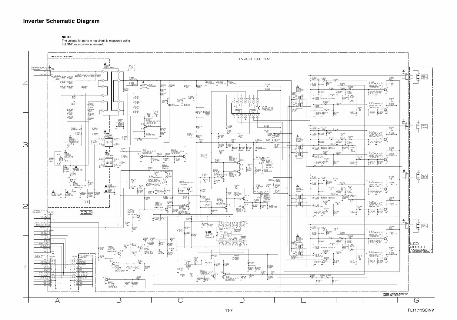
11-7
V+
V-141312111098
27 45 3 16
IC1700BA10324AF-E2
KTC3198-Y-AT/P
Q1621
4
3 2
1
IC1930LTV817MCF
4
3 2
1
IC1931LTV817MCF
KTC3198-Y-AT/PQ1971
KTC3198-Y-AT/PQ1972
820P/1KVC1990
31DF4-FCD1990
D1973
KTC3198-Y-AT/PQ1931
OPENC1934
0.1/100V
C1933
D1940
CN19002ACL
8
7
3
4
2
14
10
11
5
15
T1950POWER TRANS
1HOT-GND
2200P/250VC1905
C1940
0.027/100V
C1932
OPENC1906
2SC2120-YQ1932
D1933
820P/2KV
C1930
1000P/100V
C1931
D1932
KTC3200-GR-AT/PQ1970
0.047/100V
C1970
0.01C1981
30KR1976
82R1933
30KR1975
82R1932
180R1934
47R1930
820KR1987
1KR1986
R1946
47KR1931
220KR1941
360R1980
27KR1977
R1948
0.33/2WR1937
1.5KR1935
330KR1943
1KR1988
2.2KR1939
390KR1945
270R1970
2.7KR1982
220KR1940
330KR1944
120KR1942
R1947
180R1936
6.8KR1979
5V6BSB-T26D1970
5V6BSB-T26D1931
27BSB-T26D1930
39BSB-T26D1934 OPEN
D1935
OPENC1983
470/100V
C1992
270/200V
C1910
100/100VC1052
0.01C1068
D1071
390R1068
KTC3198-Y-AT/PQ1061
D1062 KTC3198-Y-AT/PQ1060
10/50VC1067
15P/6.3KVC1061
D1067D1060
1500PC1066
D1064
D1063
D1066
18KR1063
8.2KR1070
0.01C1064
27KR1071
8.2KR1064
15P/6.3KVC1065
D1061
390R1062
D1070
27KR1065
1500PC1062
D1068
10/50VC1063
18KR1069
D1065
D1069
100KR1060
20KR1061
D1073
100KR1066 D1074
D1072
20kR1067
CN105021
D1114
1500PC1112
20kR1117
D1119
20KR1111
390R1118
D1111
D1110
100KR1110
0.01C1114
D1120
15P/6.3KVC1111
D1121
D1112
18KR1119
D1113
27KR1115
KTC3198-Y-AT/PQ1110
D1118
8.2KR1120
D1122
390R1112
8.2KR1114
D1116
CN11002
1500PC1116
D1115
10/50VC1113
27KR1121
15P/6.3KVC1115
D1117
D1123
D1124KTC3198-Y-AT/PQ1111
10/50VC1117
0.01C1118
100KR1116
1
18KR1113
D1164
1500PC1162
20kR1167
D1169
20KR1161
390R1168
D1161
D1160
100KR1160
0.01C1164
D1170
15P/6.3KVC1161
D1171
D1162
18KR1169
D1163
27KR1165
KTC3198-Y-AT/PQ1160
D1168
8.2KR1170
D1172
390R1162
8.2KR1164
D1166
CN11502
1500PC1166
D1165
10/50VC1163
27KR1171
15P/6.3KVC1165
D1167
D1173
D1174KTC3198-Y-AT/PQ1161
10/50VC1167
0.01C1168
100KR1166
1
18KR1163
D1214
1500PC1212
20kR1217
D1219
20KR1211
390R1218
D1211
D1210
100KR1210
0.01C1214
D1220
15P/6.3KVC1211
D1221
D1212
18KR1219
D1213
27KR1215
KTC3198-Y-AT/PQ1210
D1218
8.2KR1220
D1222
390R1212
8.2KR1214
D1216
CN12002
1500PC1216
D1215
10/50VC1213
27KR1221
15P/6.3KVC1215
D1217
D1223
D1224KTC3198-Y-AT/PQ1211
10/50VC1217
0.01C1218
100KR1216
1
18KR1213
OPENC1991
OPENR1974
3.9KR1971
3.9KR1969
3.9KR1968
3.9KR1967
1ZB100BBD1994
33KR1983
15KR1984
0.47/50VC1982
1MR1072
0.1C1072
1MR1122
0.1C1122
1MR1172
0.1C1172
1MR1222
0.1C1222
GND 5
GND 9
12BACKLIGHT-ADJ11BACKLIGHT-SW
VCOM 2
INV+16V 14
VGH 6
10PROTECT3
13GND
CN1001GND 15
LCD+16V 8LCD+16V 7
P-ON+3.3V 4LCD-6.8V 3
GND 1
GND 9
GND 5
LCD+16V 3
VCOM 10
VGH 4
LCD+16V 2
P-ON+3.3V 6
LCD-6.8V 8
CN1003GND 1
BC1931BEAD
BC1930BEAD
P-ON+3.3V 7
GND 11
68KR1972
100/100VC1056
100/100VC1053
D1700
D1701
D1702
D17030.22C1702
2SC2120-YQ1501
2SA950-OQ1502
470P/2KVC1550
470P/2KVC1500
33KR1041
10R1501
20BSB-T26D1500
12KR1500
R162110K 1000P
C1620
100KR1620
KTC3198-Y-AT/P
Q1600 R160110K OPEN
C1601
18KR1600
0.1C1600
OPENC15010.01
C1502
KTC3198-Y-AT/P
Q1503
150R1502
2.2KR1503
3900P/100V
C1012
12KR1043
0.47C1040 OPEN
R1042
220KR1005
0.1C1004
56KR1006
10KR1007
82KR10092.2K
R1008
15BSB-T26
D1000
1KR1701
9.1KR1700
0.22C1703
36BSB-T26D1040
0.39/2W
R10400.39/2W
R1044
20BSB-T26D1550
10R1551
12KR1550OPEN
C1551
150R1552
2SC2120-YQ1551
2SA950-OQ1552
2.2KR1553
100KR1811
KTC3198-Y-AT/P
Q1553
0.01C1552
1KR1505
2.2KR1504
1KR1506
1KR1555
2.2KR1554
3.3KR1023
220R1026
22KR1080
OPENR1027
KTC3198-Y-AT/PQ1001
36KR1028
KTC3198-Y-AT/PQ1003
15KR1031
22KR1030
0.1C1011
D1003
5.6KR1081 24K
R1032WIRED1004
10KR1021
0.1C1008
R103610K
KTC3198-Y-AT/P
Q1005 10KR1034
4.7KR1810
KTC3198-Y-AT/P
Q1802
1.5KR1809
10BSB-T26D1801
1KR1807
5.1KR1808
0.1C1802
100/25VC1800
WIRED1802
10KR1630
D1630
3.3KR1631
12KR1812
KTC3198-Y-AT/P
Q1804
KTC3198-Y-AT/P
Q1803
22KR1802
22KR1806
1.2R1804
1KR1805
4.7KR1803
KTC3198-Y-AT/PQ1800
10KR1800
22/35VC1801
22KR1801
0.1C1001
0.1C1013
0.01C1002
22KR1001
1KR1002
100KR1003
0.1C1003
0R1004
4.7KR1014
7.5KR1015
120KR1016
10KR10170.1
C1006
100KR1024
OPENR1025
D1006
2.2KR1022
6800PC1014
KTA1267-GR-AT/P
Q1004
10KR1033
WIRER1019
2.2KR1018
WIRED1005
0.1C1007
WIRED1001
12KR1012
10KR1011
0R1010
0.1C1005
OPEND1961
OPEND1960
WIREBC1301
0R1981
100/25VC1009
2SA950-OQ1815
KTA1267-GR-AT/PQ1801
HZZS33NB2TE-EQD1971
22KR1973
1KR1556
9
1 8
16
2
11
4 6
15 10
3
1214
5
13
7
PWMCONTROLLOGIC
DRIVE
GND
VCCCTLV-REF
DRIVEOSCDTC
IC1000TL494CDR
2SK2417Q1550
G
SD
2SK2417Q1500
G
SD
TK8A50DQ1930
G
S
D
R10353.3K
T1050INVERTER TRANS
2
1
4
3 5
6
7
8
T1100INVERTER TRANS
2
1
4
3 5
6
7
8
T1150INVERTER TRANS
2
1
4
3 5
6
7
8
T1200INVERTER TRANS
2
1
4
3 5
6
7
8
BC1500BEAD
BC1550BEAD
BC1551BEAD
BC1501BEAD
OPENR1020
OPENC1010
OPEND1002
OPENC1000
OPENR1045
D1972
OPENC1054
OPENC1204
OPENC1205
OPENC1055
OPEND1050
OPENC1050
OPENR1050
OPENR1051
OPEND1051
OPENC1051
GND5
P-ON+3.3V7
VGH4
LCD-6.8V8
LCD+16V2LCD+16V3
GND11
P-ON+3.3V6
VCOM10GND9
CN1005GND1
330KR1991330KR1990
330KR1989
B
2
EA
4
F
1
3
C D
BACKLIGHT
0.4
(COMPARATOR)
0.4
15.7
0
0.4
2.5
BACKLIGHT
2.6
2.5
BACKLIGHT
0.4
BACKLIGHT
LCDMODULEASSEMBLY
G
HOT CIRCUIT. BE CAREFUL.
HOT
COLD
INVERTER CBA
TO POWER SUPPLY CBA CN602
(SWITCHING)
(SWITCHING) (ISOLATOR)
(FEEDBACK)
(SWITCHING) (SWITCHING)
82.0
81.0
1.1
00
0.4
0
0.21.1 3.3
0
0.3
0
3.40
0
0.2
10.4
6.60.2
0.2
6.6
134.8
(SWITCHING)
(SWITCHING)
5.8
6.381.0
0
6.68.4
0.70
0
0
OVER VOLTAGEPROTECTOR
0.70
OVER VOLTAGEPROTECTOR
0.7
OVER VOLTAGEPROTECTOR
0.7
0
0
0
OVER VOLTAGEPROTECTOR
0
0.7
OVER VOLTAGEPROTECTOR
0.7
0
0
0
OVER VOLTAGEPROTECTOR
0
0.7
OVER VOLTAGEPROTECTOR
0.7
0
0
0
OVER VOLTAGEPROTECTOR
0
TO POWER SUPPLY CBA CN201
TO LCD MODULEASSEMBLY
15.5(DRIVE)
4.0 3.9
3.9
(DRIVE)0
4.0
3.9
0.2
82.5
0
3.40.1
0
0.3(SWITCHING) 4.0
(DRIVE)
3.915.5(DRIVE)
4.0
3.9
0-0.3
4.0
0
(SWITCHING)
3.6
0
0.5(SWITCHING)
(SWITCHING)
(SW+16V)
(SWITCHING)
(SWITCHING)
(SW+16V)
(SWITCHING)
(SWITCHING)
(SWITCHING)
(SWITCHING)
SWITCHINGBACKLIGHT-ON
SWITCHINGBACKLIGHT-ON
1.3 1.6 0 3.73.11.7
0
1.3 3.6
5.1 0
PWM CONTROL
15.75.10.30.2 3.7
0.2
82.5 3.9
UNLESS OTHERWISE SPECIFIED:DIODES ARE 1SS133.
CURRENTCONTROLSWITCH
CURRENTCONTROLSWITCH
15.8 15.715.0
0.1
00.7
0.8
0.10
0.1
00.7
4.81.9
5.13.6
00.2
015.8
003.43.4-6.2000
15.8
15.7
15.0
15.7
0
0.80
0
3.60
3.9
0 0
0 2.5 0
15.8
0
3.43.4
0
TO LCD MODULEASSEMBLY
15.8
0
0
-6.2
0
0
OPEN OPEN OPENOPEN
OPEN
FL11.11SCINV
Inverter Schematic Diagram
NOTE:The voltage for parts in hot circuit is measured usinghot GND as a common terminal.

11-8
CL103B1AL+3.3V2GND3KEY-IN1
SW101A SW103A SW104A SW105A SW106A SW107A
0.1C108
4.7KR113
8.2KR114
220R108
2.7KR112
10KR109
18KR115
4.7KR111
OPEND107
4KEY-IN2
10KR152
WIRER151
0.1C151
OPEND151
SW153
2.2KR154
SW151 SW152
2.2KR153
SW154 SW155
OPENR156
OPENR155
SW101B SW104B SW103B SW105B SW107B SW106B
2
1
A B C
FUNCTION CBA
TO IR SENSORCBA CL103C
CH UP VOLDOWN
POWER MENU
UNLESS OTHERWISE SPECIFIED:SWITCHES ARE SKHHLMA0100.
STOP EJECTPLAYCHDOWN
VOLUP OPENOPEN
VOLDOWN
POWER CHDOWN
MENU VOLUP
CH UPOPEN OPEN OPEN OPEN OPEN OPEN
FL11.11SCF
Function Schematic Diagram
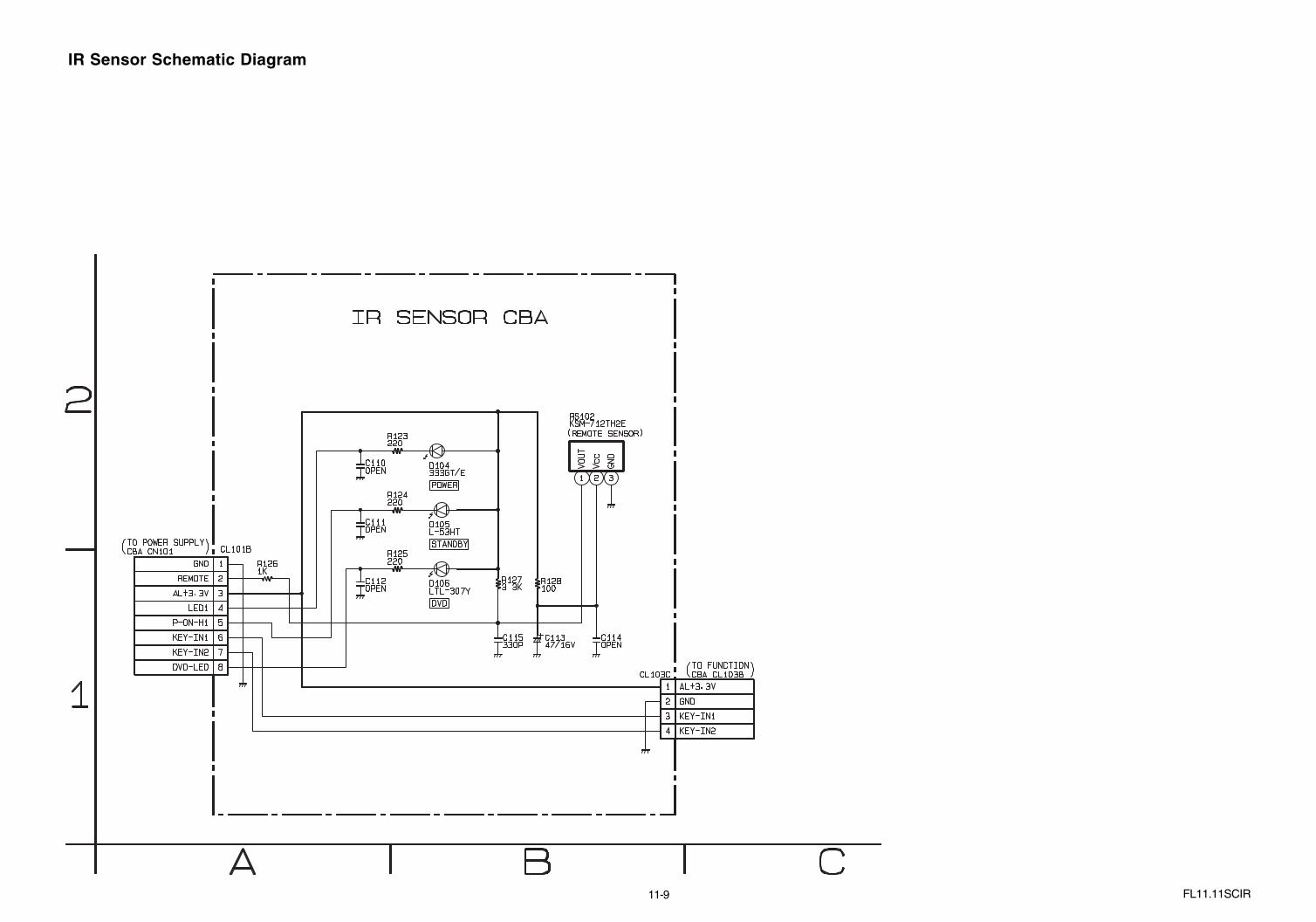
11-9
100R128
6KEY-IN15P-ON-H1
220R124
CL101B1GND
L-53HTD105
2 GND
47/16VC113
CL103C1 AL+3.3V
OPENC114
1KR126
2REMOTE
OPENC111
4LED1Vcc
GND
VOUT
2 31
RS102KSM-712TH2E
3.3KR127
3 KEY-IN1
220R123
330PC115
3AL+3.3V
OPENC110
333GT/ED104
4 KEY-IN2
OPENC112
220R125
LTL-307YD106
7KEY-IN28DVD-LED
IR SENSOR CBA
POWER
(REMOTE SENSOR)
A
TO FUNCTIONCBA CL103B
B
TO POWER SUPPLYCBA CN101
2
C
1
STANDBY
DVD
FL11.11SCIR
IR Sensor Schematic Diagram

11-10
1 STV
3 OE1
6 TP
4 CPV5 POL
2 XA0
CN300524 GND
13 LLV3(+)
10 LLV4(-)
15 LLVCLK(-)16 LLVCLK(+)
12 LLV3(-)
19 LLV2(+)
11 LLV4(+)
18 LLV2(-)
23 LLV0(+)
20 LLV1(-)21 LLV1(+)22 LLV0(-)
AA12
AA13AB13
W13Y13
W12Y12
W11Y11
AB14AA14
AA11AB11
AB16AA16AB15AA15
AB17
AB12
W14REFR
17 GND
14 GND
9 LLV5(+)8 LLV5(-)7 GND
1KR3152
P-ON+3.3V
0R3126
0R3128
OPENR3127
OPENR3129
RESET-LCD
OPENR3124OPENR3125
0R3164
0R3170
0R31670R3168
OPENR3116OPENR3117
0R31120R3114
TPPOL
12 RX3(-)
1 GND
20 RX1(-)21 RX1(+)
17 GND
11 NU
3 GND4 GND
15 RXCLK(-)
22 RX0(-)
13 RX3(+)
18 RX2(-)
7 GND
19 RX2(+)
8 NU
24 GND
5 GND
16 RXCLK(+)
9 NU
2 GND
6 GND
10 NU
23 RX0(+)
14 GND
25 GND26 GND27 LCD+12V28 LCD+12V29 LCD+12V
CN300431 LCD+12V30 LCD+12V
Q3001OPEN
1 2 3 4
5678
Q3002OPEN
OPEN
R3161
LCD+12V
OPENC3078
OPENR3007
OPENR3006
OPENC3002
OPEN
R3155
OPENR3113OPENR3115
0R3165W16Y16
0R3166
OPENR3118OPENR31190R3120
OPENR3121
0R3122
OPENR3123
0R3163
OPEN
R3157
OPEN
R3159
OPEN
R3160
OPEN
R3162
OPEN
R3158
CPVOE
STV
0R3169
5.6KR3088
*1IC3005(1/6)R8J04013BG-RJ
AA17
Y15W15
OPENR3002
OPENR3001
RESET-LCD
20DVD-Pb
22DVD-Y
26DVD-AUDIO(R)
13DVD-SCLK
19GND
14GND
27GND
12GND
10GND
23GND
25DVD-AUDIO-MUTE
6DVD-P-ON
16LED-CONT
4P-ON-H3(NU)
11DVD-CS
21GND
2KEY-IN2
9DVD-DISC-IN
5DVD-MAIN-PWR
17GND
3DVD-LED
1GND
18DVD-Pr
24DVD-AUDIO(L)
DVD-SPDIF 28
8DVD-SDATA7DVD-REMOTE
CN3003GND 29
15DVD-DISC-OUT
33PC3269
33PC3267
33PC3294
100PC3272
OPENC3296
OPENC3266
680R3473
33PC3268
680R341933P
C3295
100PC3273
100R3417
100R3471
100PC3270
1000PR3418
100R3420
1000PR3474
100PC3271
100R3472
100R3425
100R3426
100R3427
100PC3274
100R3428
100PC3275
100R3429
100PC3277
100R3430
100PC3278100P
C3279
100R3432
100PC3280
100R3433
1000PC3281
DVD-AUDIO-MUTE
DVD-AUDIO(L)DVD-SPDIF
DVD-AUDIO(R)
KEY-IN2
DVD-P-ONDVD-SDATA
LED-CONT
DVD-DISC-IN
DVD-Pr
DVD-CS
DVD-Pb
DVD-REMOTE
DVD-DISC-OUT
DVD-SCLK
DVD-Y
DVD-MAIN-PWRDVD-LED
100PC3276
DIGITAL SIGNAL PROCESS/MAIN MICRO CONTROLLER
TO LCD MODULEASSEMBLY
LVDSTX
TO DIGITAL MAIN 2IC3005(2/6)
CONTINUEDIGITAL 5
CONTINUEDIGITAL 5
DIGITAL MAIN CBA UNIT
CONTINUEDIGITAL 4
TO LCD MODULEASSEMBLY
DC
2
4
B
1
E FA
3
CONTINUEDIGITAL 2
TO POWER SUPPLY CBA CN303
CONTINUEDIGITAL 3
CONTINUEDIGITAL 4
CONTINUEDIGITAL 2
FL11.11SCD1
Digital Main 1 Schematic Diagram
The order of pins shown in this diagram is different from that of actual IC3005. IC3005 is divided into six and shown as IC3005 (1/6) ~ IC3005 (6/6) in this Digital Main Schematic Diagram Section.
1 NOTE:

11-11
GND7
COM-VIDEO-Y-IN15
GND1
GND9S-VIDEO-Y-IN8
SPDIF2
RESET23
AUDIO-MUTE20
CN3006KEY-IN129
GND25
S-VIDEO-C-IN6
COM-VIDEO-Pr-IN19
GND16COM-VIDEO-Pb-IN17
VIDEO-IN4
33PC3107
33PC3104
33PC3103
33PC3093
33PC3095
33PC3098
1000PC3092
1000PC3074
100R3404
100PC3111
A8B7
A12
D8
C14
B12A11
D9
C11C8
0.1C32010.1C3202
0.1C3203
0.1C3200
0.01C3197
0.1C31990.1C3198
OPENC3196
OPENC3194OPENC3195
DIF-OUT228
DIF-OUT126
IF-AGC24
AUDIO(R)11INPUT012
SCL22SDA21
AUDIO(L)13
33PC3100
SDASCL
AUDIO-MUTE
F2
J1IF-AGC
22R3188
Y18HDMA-SCLW19HDMI-SDA
SPDIF
GND3
S-VIDEO-SW5
1000PC3105
100R3175
INPUT110
33PC3102
22R3187
100R3171AUDIO(R)
100R3154AUDIO(L)
GND14
GND18
100R3144100R3142100R3138
100R3134
GND27
KEY-IN1
AB22S-VIDEO-SW
K1INPUT0L4INPUT1
0R3179
100PC3099
OPENC3084
P-ON+5V
100PC3101
100PC3112
0R3181
OPENR3180
Q3010OPEN
OPENR3184
OPENR3185
LIGHT-SENSRESET
OPENR3356 D3049
OPEN
OPENR3364
OPENR3284
1
2
3
4
5
14
13
12
11
15
6
7
8
9
10
JK3001(OPEN)D-SUB CONNECTOR
D3055OPEN
D3053OPEN
OPENR3377
OPENR3285
OPENR3286
OPENR3376D3040
OPEND3027OPEN
1
2
3
4 5
6
7
8
IC3012(OPEN)
A0
A1
A2
GND SDA
SCL
WP
VCCOPENC3211
OPENR3310
OPENR3326
OPENR3333
D3041OPEN
Q3012OPEN
Q3011OPEN
4.7KR3193
4.7KR3192
OPENR3321
OPENR3334
D3054OPEN
1
2
3 4
VCC
GND
5
IC3013(OPEN)
1
2
3 4
VCC
GND
5
IC3014(OPEN)
OPENC3214
AL+3.3V-2
B15VSINB14HSIN
OPENR3296
OPENR3295
OPENR3339
OPENR3347 D3045
OPEN
OPENR3358 D3050
OPEN
OPENR3343
M19DVD-DISC-OUT
B10NU0.1C3210
A6NU0.1C3209
A9NU0.1C3208
B11NU0.1C3207
B13NU0.1C3206
A14NU0.1C3205
A13NU0.1C3204
B9NUE3NUC9NUB6NU
OPEN
C325
6
OPEN
C325
7OP
ENC3
258
OPEN
C325
9
OPEN
C325
5OP
ENC3
254
0R34000R3399
0R3398
0R3401
0R3403
0R3402
OPENR3183
OPENR3186
D3056OPEN
RESET-LCD
F1
IC3005(2/6)R8J04013BG-RJ
*1
C7NUA10NU
OPENR3298
OPENR3297N21DVD-DISC-IN
OPENR3467OPENR3466
10PC3225
10PC3226
0R3338
0R3337
L30220.27uH
0R3345
0R3344
33PC3235
L3024OPEN
L3023OPEN
0R3353
0R3354
OPENC3243
OPENR3369
0R3361
0R3360
OPENC3242
OPENR3368
2.2KR3202
0.1C3178
2.2KR3194
0.33C3177
22R3218
HDMI-SDAHDMI-SCL
33PC3089
A1 NU0.1C3219
10C3220
E2 NU0.1C3221
E1 NU0.1C3222
1000PC3086
33PC3087
10KR3190
10KR3189
100R3156
100R3172
P-ON+3.3V
WP
OPENR3416
22R3228
22R3229
OPENC3293
OPENC3292
OPENC3291
A15NUC12DVD-YA7DVD-PbB8DVD-Pr
0.1C3285
0.01C32900.1C3284
0.1C3286
0R34580R34590R3460
OPEN
C328
7
OPEN
C328
9OP
ENC3
288
OPEN
R347
6OP
ENR3
477
OPEN
R347
8
W18DVD-REMOTER3437 10K
Q30332SC4081UBTLQ
10KR3436
R3435 100
DVD-Y
DVD-PrDVD-DISC-OUT
DVD-Pb
DVD-REMOTEDVD-DISC-IN
22R3219
4
JI
3
2
L
1
G H K
DIGITAL MAIN CBA UNIT
TO POWER SUPPLY CBA CN302
DIGITAL SIGNAL PROCESS/MAIN MICRO CONTROLLER
CONTINUEDIGITAL 4
CONTINUEDIGITAL 3
SW
A/DCONVERTER
DEMODULATOR/MPEGDECODER
DIGITALSIGNALPROCESS
TO DIGITAL MAIN 6IC3005(6/6)
TO DIGITAL MAIN 1IC3005(1/6)
CONTINUEDIGITAL 3
TO DIGITAL MAIN 3IC3005(3/6)
(MEMORY)
(BUFFER GATE)
(BUFFER GATE)
CONTINUEDIGITAL 1
CONTINUEDIGITAL 6
CONTINUEDIGITAL 5
CONTINUEDIGITAL 1
(BEFFER)
(BUFFER)
(BUFFER)
FL11.11SCD2
Digital Main 2 Schematic Diagram
The order of pins shown in this diagram is different from that of actual IC3005. IC3005 is divided into six and shown as IC3005 (1/6) ~ IC3005 (6/6) in this Digital Main Schematic Diagram Section.
1 NOTE:

11-12
L3ACLK
1 2 3 4 5 6 7
910
8
1112131516 14GND VCC NUNU
ENHANCEDMULTI-LEVELDELTA-SIGMAMODULATOR
ZERO DETECT
4X/8XOVERSAMPLINGDIGITAL FILTER/FUNCTIONCONTROLLER
LPFLPF DAC
DAC
AUDIOSERIAL PORT
SYSTEMCLOCKMANAGER
SERIALCONTROL PORT
IC3010PCM1782DBQR
L1BCLK
M2
22R3196
22R3198
22R3195
22R3197
G1G2
0.1C3215G3NU
10C3216
C410C3217
AUDIO(L)
B510C3218
AUDIO(R)
C3NUC1C2NUB2NU
AA10SRXD0Y10SCLK0
AB10STXD0
SPDIF
AUDIO(L)-OUT
OPENR3174
OPENR3173
AUDIO(R)-OUT
10C3108
0.1C3110
10C3109
L3013BLM21PG221SN1D
P-ON+5V
AMP(L)-OUTAMP(R)-OUT
0R3176
0R3177
L2SPDIF
18KR333518KR3336
OPENR3331
OPENR3327
22R320022R3201
22R3199
100R3209
GND
VCCIC3015NJM4558M(TE1)
1 2 3 4
5678
82PC3237
3.9KR3355
68KR3350
4.7KR3342
4.7KR3332
82PC3232
82PC3229
4.7KR3325
10C3224
OPENC32450R3362
OPENR3320
12KR3393
12KR3394
10C3249
220PC3248
0.1C3250C3251
100/16V
L3038BLM21PG221SN1D
3.9KR3352
68KR3351
82PC3241
82PC3230
4.7KR3330
4.7KR3341
10C3223
4.7KR3322
82PC3227
0R3359
OPENC3244
OPENR3311
B1NU
A2B4NU
A5NUA4NUA3NU
B3NU
K20P-ON-H2
J21LED-R
VCOM-PWM
P-ON-H2
AB21VCOM-PWM
K21REMOTE
REMOTE
LED-R
MADIN0
G21KEY-IN1H19MADIN0
KEY-IN1LIGHT-SENS
G20KEY-IN2H21PROTECT1
PROTECT1
G22PROTECT2
PROTECT2
H22PROTECT3
PROTECT3
H20DTV-ON-H2
DTV-ON-H2
M3DVD-AUDIO-MUTE100R3208
M21DTV-ON-H1100R3210
DTV-ON-H1
J19HDMI-HPD122R3211
HDMI-HPD1
22R3212J20HDMI-HPD0
HDMI-HPD0
22R3213
K22HDMI-CEC
HDMI-CEC
P18NU22R3214
J22HDMI-HPD2
HDMI-HPD2
100R3205
OPENR3313
22R3318
22R3312
22R3316
22R3314
22R3317
22R3315
M1
*1IC3005(3/6)R8J04013BG-RJ
LRCLK
10KR3178 100
R3191
RESET
0.1C3106
0.1C3252
4.7KR3182
32
1 4
IC3009PST8420UR
CDVDD
GND OUT
T20RESET-N
0.033C3113
OPENC3116
0.01C3120
AL+3.3V
CPU-RESET-N
10C3282 22R3444
10KR3446
10C3283
10KR3447
1KR3445
100KR3475
22R3465
1
2
3 4
VCC
GND
5
IC3017SN74LVC1G126DCKR
1
2
3 4
VCC
GND
5
IC3016SN74LVC1G126DCKR
100R3439
100R3440
OPENR3438
P-ON+3.3V
L3040BLM21PG221SN1D
C7-SPD-ENDVD-SPD-EN
DVD-AUDIO(L)DVD-SPDIFDVD-AUDIO-MUTEDVD-AUDIO(R)
KEY-IN2
4
PO
3
2
R
1
M N Q
DIGITAL SIGNAL PROCESS/MAIN MICRO CONTROLLER
AUDIOI/F
CONTINUEDIGITAL 2
DIGITAL MAIN CBA UNIT CONTINUEDIGITAL 5
TO DIGITAL MAIN 2IC3005(2/6)
TO DIGITAL MAIN 6IC3005(6/6)
AUDIO D/ACONVERTER
(OP AMP)
CONTINUEDIGITAL 4
CONTINUEDIGITAL 2
CONTINUEDIGITAL 5
CONTINUEDIGITAL 6
(RESET)
(BUFFER GATE)
(BUFFER GATE)CONTINUEDIGITAL 4
CONTINUEDIGITAL 1
Digital Main 3 Schematic Diagram
FL11.11SCD3
The order of pins shown in this diagram is different from that of actual IC3005. IC3005 is divided into six and shown as IC3005 (1/6) ~ IC3005 (6/6) in this Digital Main Schematic Diagram Section.
1 NOTE:

11-13
IC3002K4T51163QG-HCF7
*A VDD J2VREF
E2 NUK2CKEJ8CKK8CKL8CSK7RASL7CASK3WEL1BA2/NUL3BA1L2BA0R2A12P7A11M2A10/APP3A9P8A8P2A7N7A6N3A5N8A4N2A3M7A2M3A1M8A0K9ODT
*BVSS
A2 NUR8 NUR7 NUR3 NU
B7 UDQSA8 UDQS/NUB3 UDMB9 DQ15B1 DQ14D9 DQ13D1 DQ12D3 DQ11D7 DQ10C2 DQ9C8 DQ8F7 LDQSE8 LDQS/NUF3 LDMF9 DQ7F1 DQ6H9 DQ5H1 DQ4H3 DQ3H7 DQ2G2 DQ1G8 DQ0
N4 SD-DQ14T2 SD-DQ13R4 SD-DQ12P4 SD-DQ11R2 SD-DQ10R3 SD-DQ9R1 SD-DQ8V1 SD-DQ7T4 SD-DQ6W2 SD-DQ5V4 SD-DQ4W3 SD-DQ3W1 SD-DQ2U4 SD-DQ1V2 SD-DQ0N3 SD-UDMU3 SD-LDMP1 SD-UDQSNN2 SD-UDQSU1 SD-LDQSNU2 SD-LDQS
AB2 SD-RASAA3 SD-CASW6 SD-WE
AA1 SD-CLKNY2 SD-CLKW8 SD-CKEAA2 SD-ODTAB8 SD-A12
Y8 SD-BA2
W7 SD-A1
AA4 SD-A4
W5 SD-A2
AA5 SD-A8AA7 SD-A9
AA8 SD-A7
Y6 SD-BA1
AB5 SD-A11
AB4 SD-A6
AB3 SD-A0
AB7 SD-A3
AB6 SD-A10
W9 SD-BA0
AA6 SD-A5
100R3026
0.1C3009
0.1C3010
100R3027
H2USB(+)H1USB(-)
P-ON+5V
1
2
3
4 5
6
7
8
IC3006W25X32VSSIGE
CS
SO
WP
GND SI
SCK
NU
VCC
K2SDAK3SCL
SCLSDA
4.7KR3204
4.7KR3203
3USB(+)4GND
2USB(-)
CN30091USB+5V
1C3246 Q3009
2SB1732TL
330R3151
330R3153
10KR3150 1
C30961KR3146
10KR3147
15KR3148
MADIN0
D3002AS431AKTR-E1 33K
R3140
33KR3139
180R3141
2.4R3135
1.6R3136
Q30082SC4081UBTLQ
10KR3108
Y20 CS
0.1C30290.1C30300.1C30310.1C30320.1C30330.1C30340.1C30350.1C30360.1C30370.1C30380.1C30390.1C30400.1C30410.1C3042
OPENC3091
10KR3104
P-ON+3.3VAL+3.3V
P-ON+1.8V
AA9 NU
4.7R30244.7R3015
22R3048
22R3038
22R3031
22R303522R303622R3037
22R3016
22R302922R3030
22R304022R3039
22R304122R304222R3043
22R3047
22R304522R3046
22R3044
22R3032
22R303422R3033
Y4 SD-CS22R3028
120R3049
2 UART0-TXR20RXD0
OPENC3253
3 UART0-RX
4.7KR3395
4 GND4.7KR3396
R19TXD0
CN30101 P-ON+5V
L3004BLM21PG221SN1D
10KR3107
10KR3102
L3025 EXC24CG900U D3052OPEN
47R308947R3092
47R3093 22R320622R3207
AB18OE222R3090
OE2
47R3091
W20BACKLIGHT-SW22R3095
Y22P-ON-H122R3096
4.7KR3098
BACKLIGHT-SW
P-ON-H1
U19DVD-MAIN-PWRV20DVD-P-ON
W21USB-EN
W22DVD-SPD-ENV21GPIO6
J3NU6.04KR3099
F22NU10C30760.1C3075
J4NU10C30720.1C3071
H3NU
GPIO6
22R3131
IC3005(4/6)R8J04013BG-RJ
*1
R5 SD-VREF0
P2 SD-DQ15
V7 SD-VREF1
0.1C3051
100R3065
0.1C3050
100R3064
POLAB20OE
K19LED1
CPV
AB19TP
LED1
AA19STV
Y19POL
OE
AA18CPVSTV
TP
0.1C3073 130R3070
130R3071
100R3421
100R3422
CN3007P-ON+5V1
2 UART0-TX3 NU4 NU5 UART0-RX6 M32TDI
9 M32TRST-N10 RESET-LCD11 GND
8 M32TDO7 AL+3.3V
14 ASEMD015 TRST-N16 TCK
13 ASEBRKAK-N12 M32TMS
19 TMS20 CPU-RESET-N
18 TDO17 TDI
U21DVD-CS
T19DVD-SDATAU22M32TRST-N
10KR3224
V22RESET-LCD
U20DVD-SCLKP22ASEBRKAK-NR21ASEMD0P19TRST-NP20TCKP21TDIM22TDON22TMS
CPU-RESET-N
L22GPY10
GPY10
L19AUDIO-MUTE
10KR3234
22R3233
AUDIO-MUTE
22R323222R3231
AA20NU10KR323022R321722R321622R3215
RESET-LCD
W17BACKLIGHT-ADJ100R3227
BACKLIGHT-ADJ
Y17C7-SPD-EN22R3225
L20DVD-LED
CPU-RESET-N
OPENR3441
L3041BLM21PG221SN1D
OPENR3450
100R3470
22R3442
100R3469
100R3468
22R3448
22R3449
L21LED-CONT22R322622R3451
OPENR3453
C7-SPD-ENDVD-SPD-EN
OPENR3452
22R3443 100R3463
100R3461100R3462
DVD-SCLK
DVD-SDATA
DVD-MAIN-PWR
DVD-CS
DVD-LED
DVD-P-ON
LED-CONT
1MR3235
T22XIN25
15PC3183
X300125MHzT21XOUT25
510R3223
15PC3184
AA21 WPAA22 SOUT
Y21 SIN
47R3094V19 SCK
22R3454
L3043BLM21PG221SN1D
DIGITAL MAIN CBA UNIT
DIGITAL SIGNAL PROCESS/MAIN MICRO CONTROLLER
(DDR2 SDRAM)
*B:A3,A7,B2,B8,D2,D8,E3,E7, F2,F8,H2,H8,J3,J7,N1,P9
*A:A1,A9,C1,C3,C7,C9,E1,E9, G1,G3,G7,G9,J1,J9,M9,R1
1-V32-V33-V3
4-V35-V36-V3
SD-DQ8SD-DQ14SD-DQ15SD-DQ12SD-DQ11SD-DQ10SD-DQ9SD-DQ13
SD-DQ7SD-DQ6SD-DQ5SD-DQ3SD-DQ4SD-DQ2SD-DQ1SD-DQ0
SD-DQ2
SD-DQ5
SD-DQ1
SD-DQ4
SD-DQ0
SD-DQ7
SD-DQ3
SD-DQ6
SD-DQ13
SD-DQ9
SD-DQ12
SD-DQ8
SD-DQ15
SD-DQ11
SD-DQ14
SD-DQ10
1-S32-S3
3-S3
4-S35-S3
6-S3
(MEMORY)
(USB JACK)
(SW+5V)
(SWITCHING)
CONTINUEDIGITAL 5
2
S V
1
T U
3
4
W X
(NO CONNECTION)
CONTINUEDIGITAL 1
CONTINUEDIGITAL 5
(NO CONNECTION)
CONTINUEDIGITAL 2
CONTINUEDIGITAL 3
CONTINUEDIGITAL 6
CONTINUEDIGITAL 3
CONTINUEDIGITAL 1
Digital Main 4 Schematic Diagram
FL11.11SCD4
The order of pins shown in this diagram is different from that of actual IC3005. IC3005 is divided into six and shown as IC3005 (1/6) ~ IC3005 (6/6) in this Digital Main Schematic Diagram Section.
1 NOTE:

11-14
P-ON+3.3V19
21 AL+3.3V
P-ON-H21
GND23OE224
P-ON+3.3V20
P-ON-H19
REMOTE25
GND3
P-ON+5V13
BACKLIGHT-ADJ28
BACKLIGHT-SW26
CN3002VCOM-PWM29
BACKLIGHT-SW
0.1C3016
0.1C3022
P-ON-H1
1000PC3055
1000PC3067
0.1C3047
*AVDD12
AL+3.3V
P-ON+5V14
10C3045
AUDIO(L)-OUT2
100R3087
AUDIO(R)-OUT4
100R3085
PROTECT35AMP(L)-OUT6
100R3078
GND7
100R3074
AMP(R)-OUT8
P-ON+3V10PROTECT111
1000PC3048
100R3101
100R3072
GND12
PROTECT215
1000PC3044
P-ON+7V160.1C3043
10C3028
1
2
3
4 5
6
7
8
IC3008BD9321EFJ-E2
BST
VIN
SW
GND FB
COMP
EN
SS
0.015C30886.8KR3137
15KR3143
6.04KR3145
0R3149
L300910uH
D3001SK22A
0.1C3085
0.1C3082
10C3081
10C3080
0.1C3083
1C3090
1 2 3 4 5
IC3007BD7820FP-E2
CTL
VCC
GND
OUT
C
1KR31111K
R3110
390R3109
GND17GND1810
C3019
22 AL+3.3V
10C3015
1 2 3 4 5
IC3004BD7820FP-E2
CTL
VCC
GND
OUT
C
1KR3060
390R3059
1KR3061
100R3017OE2
100PC3008
100R3014
LED127
100R3008
100R3009
100R3010
1000PC3005
LED1
100R3011
1000PC3006
AUDIO(L)-OUTAUDIO(R)-OUTAMP(L)-OUTAMP(R)-OUT
P-ON+5V
AL+3.3V-2
P-ON+5V
P-ON+3.3V
100PC3003
1000PC3061
1000PC3057
1000PC3062
OPENR3063
OPENR3062
10C3097
10KR3079
*B VSS
0.1C3179
0.1C3180
IC3005(5/6)*1
R8J04013BG-RJ
K5VDDA33RU
Q30042SC4081UB-TLQ
AL+3.3V-2
LCD+12V
OPENR3005
OPENR3004
OPENR3003
BACKLIGHT-ADJ
0R3050
0R3054
Q30032SC4081UB-TLQ
2.2KR3086
2.2KR308410K
R3077
C309447/4V
0.1C3122
0.1C3123
0.1C3124
0.1C3129
0.1C3121
0.1C3128
J2VDDA33USBK4VDDA33USBR22VCC33STBL18VCC33STB
0R3220
0.1C3182
M14VDDSTB
0.1C3181
GDS
Q3013SSM3K309T
100R3221
10KR3222
GPY10
0.1C3125
0.1C3130
V10PLLDVDDN11PLLDVDDV11PLLDVDDN13PLLDVDDN14PLLDVDD
0.1C3136
0.1C3138
0.1C3137
L3015BLM21PG221SN1D
M4VCCQ33V13VCCQ33V15VCCQ33V18VCCQ33W10VCCQ33P10PLLAVCCN10PLLAVCCP11PLLAVCC
0.1C3127
0.1C3126
0.1C3131
10C3133
OPENC3134
0.1C3132
0.1C3142
0.1C3140
0.1C3145
0.1C3144
0.1C3143
10C3139
L3016BLM21PG221SN1D
0.1C3141
P13PLLAVCCT18PLLAVCC
N1VCCQ18N5VCCQ18T1VCCQ18T5VCCQ18V3VCCQ18Y1VCCQ18Y5VCCQ18Y9VCCQ18J9VDD18J10VDD18J11VDD18J12VDD18E10AVDD18E12AVDD18D13VDD18HDMIJ13VDD18HDMIE15VPPOTP
L3014BLM21PG221SN1D
100C3115
0.1C3118
10C3114
0.1C3117
0.1C3119
0.1C3146
0.1C3152
0.1C3151
0.1C3147
0.1C3150
0.1C3149
0.1C3148
OPENC3153
L3017BLM21PG221SN1D
0.1C3157
10C3155
10C3154
0.1C3156
0.1C3160
0.1C3159
0.1C3162
0.1C3161
0.01C3264
P-ON+1.8V
C3049100/4V
10C3024
10C3023C3018
100/16V
L30012uH
0.1C3027
1C3263
0.1C3070
10C3069
10C3068C3066
220/16V
BC30012.2uH
10C3052
0.1C3053
C6AVDD33C13AVDD33D2AVDD33D10AVDD33E8AVDD33E18VDD33HDMIG18VDD33HDMIE17VDD33HDMIJ18VDD33HDMID14VDD33IOH5AVDD33PLLF5AVDD33AUDD1MIXVDD33D5MIXVDD33E4MIXVDD33E5MIXVDD33F4MIXVDD33
L3019BLM21PG221SN1D
0.1C3166
0.1C3165
0.1C3170
0.1C3169
0.1C3168
10C3163
0.1C3171
10C3167
0.1C3164
0.1C3172
0.1C3175
0.1C3173
10C3176
0.1C3174
L3020BLM21PG221SN1D
D11REXTH4LPF
6.8KR3340
0.1C3228
1KR3319 0.1C3231
C3077100/16V
L3003BLM21PG221SN1D
10KR3133
PROTECT1
P-ON-H2
PROTECT2
VCOM-PWM
PROTECT3
LED-R
DTV-ON-H2
REMOTE
DTV-ON-H1
100R3068100R3058
0R3066
1000PC3046
1000PC3004
P-ON+3.3V
P-ON+3.3V
22KR3106
1KR3105
Q30052SC4081UB-TLQ
D31011SS400D31021SS400
22KR3100
2.2KR3097
C3079100/4V
Q31012SC4081UB-TLQ
47KR3423
CPU-RESET-N
100R3424 D3103
1SS400
D3104 1SS400
D31051SS400
1C3054
D31061SS400
C5 NUD4 NUE9 AVSS18E11 AVSS18C10 AVSSD3 AVSSD7 AVSSD12 AVSSE7 AVSSE13 VSSHDMIE16 VSSHDMIF18 VSSHDMIG19 VSSHDMIH18 VSSHDMIJ14 VSSHDMIE14 VSSIOJ5 AVSS33PLLG4 AVSS33AUDG5 AVSS33AUDD6 MIXVSS33E6 MIXVSS33F3 MIXVSS33L5 VSSAUSB
HDMI-VDD33
100R3083
P-ON+3.3V
AL+3.3V
0R3073
Q30062SA1774
C326510
OPENR3464
L3044BLM21PG221SN1D
P-ON+3.3V
P-ON+5V
100PC3011
1000PC3063
1000PC3065
DDAA
4
1
3
2
CCY BBZ
DIGITAL MAIN CBA UNIT
TO POWER SUPPLY CBA CN301
DIGITAL SIGNAL PROCESS/MAIN MICRO CONTROLLER
*A:L9~L14,M13,M20, N18~N20,P9,V6, V8,V16
(DC-DC CONVERTER)
(+1.8V REG.)
(+1.8V REG.)
CONTINUEDIGITAL 3
CONTINUEDIGITAL 2
CONTINUEDIGITAL 1
CONTINUEDIGITAL 3
CONTINUEDIGITAL 4
CONTINUEDIGITAL 6
(SWITCHING)
CONTINUEDIGITAL 4
*B:K9~K14,K18,M5, M9~M12,M18,N9, N12,P3,P5,P12, P14,R18,T3,U5, U18,V5,V9,V12, V14,V17,W4,Y3, Y7,Y14,AB1,AB9
(SW+3.3V)
(SWITCHING)
(SWITCHING)
(SWITCHING)
(SWITCHING)
CONTINUEDIGITAL 6
CONTINUEDIGITAL 1
Digital Main 5 Schematic Diagram
FL11.11SCD5
The order of pins shown in this diagram is different from that of actual IC3005. IC3005 is divided into six and shown as IC3005 (1/6) ~ IC3005 (6/6) in this Digital Main Schematic Diagram Section.
1 NOTE:

11-15
HDMI-SCL
16 HDMI-DATA
12 CLOCK(-)
JK30021 DATA2(+)
6 DATA1(-)
3 DATA2(-)
14 NU
9 DATA0(-)10 CLOCK(+)
7 DATA0(+)
5 TMDS DATA1 SHIELD
17 GND18 +5V
13 HDMI-CEC
15 HDMI-CLOCK
19 HOT PLUG DETECT
2 TMDS DATA2 SHIELD
4 DATA1(+)
11 TMDS CLOCK SHIELD
8 TMDS DATA0 SHIELD
P-ON+3.3VAL+3.3V-2
Q30142SK3018
27KR3237
D19C20
B21
D20
A22A21
D3057RB751S-40TE61
82KR3415
C18PWR2
13
1
15
14
16
3
6
5
11
4
7
12
10
8 9
2
IC3011BU9883FV-WE2
VCC1
SDA1
WPB
VCC-OUT
SDA0
SCL0
VCC0 VCC3
SCL3
SDA3
GND
NU
SDA2
SCL2
VCC2
SCL1
B16PWR1C15PWR0
D18EXT-RES
F21PLL-XFC-A
0.1C3192HDMI-SDA
4.7KR3455
GPI06
OPENR3261OPENR3238OPENR3239OPENR3240OPENR3241OPENR3242OPENR3243OPENR3244
OPENR3390
OPENR3381OPENR3365
OPENR3387
Q3030OPENOPEN
R3386
OPENR3408 OPEN
R3412
OPENR3370
OPENR3371
OPENR3411
OPENC3262Q3022
OPEN
OPENR3300
OPENR3292
HDMI-HPD0
15 HDMI-CLOCK
19 HOT PLUG DETECT
Q30242SK3018
1KR3372
10KR3301
Q30312SC4081UBTLQ
2 TMDS DATA2 SHIELD
6 DATA1(-)
0R3391
4 DATA1(+)
10KR3383
3 DATA2(-)
11 TMDS CLOCK SHIELD
10KR3293
HDMI-HPD1
14 NU
0R3388
0R3382
8 TMDS DATA0 SHIELD
OPENR3373
9 DATA0(-)10 CLOCK(+)
7 DATA0(+)
5 TMDS DATA1 SHIELD
17 GND
0R336616 HDMI-DATA
18 +5V
12 CLOCK(-)
1KR3407
13 HDMI-CEC
OPENR3413
JK30031 DATA2(+)
0R3392
8 TMDS DATA0 SHIELD
11 TMDS CLOCK SHIELD12 CLOCK(-)
2 TMDS DATA2 SHIELD
JK30041 DATA2(+)
OPENR3375
18 +5V
Q30322SC4081UBTLQ
10 CLOCK(+)9 DATA0(-)
10KR3302
10KR3385
19 HOT PLUG DETECT10KR3294
0R3367
13 HDMI-CEC
7 DATA0(+)
1KR3406
14 NU
16 HDMI-DATA
0R3389
4 DATA1(+)
15 HDMI-CLOCK
Q30232SK3018
6 DATA1(-)
0R3384
1C3260
HDMI-HPD2
5 TMDS DATA1 SHIELD
1KR3374
3 DATA2(-)
17 GND
OPENR3414
0.1C3212
Q30202SK3018
47KR3276
47KR3273
Q30152SK3018
4.7KR3266
4.7KR3263
C19
*1IC3005(6/6)R8J04013BG-RJ
B22
100R3405
HDMI-CEC
A16DDC0-SCLC16DDC0-SDA
D16DDC1-SDA
0R32470R32480R32490R32500R32510R3252
F19
E19
D21
C21
E20
0R3245
D22
C22
F20D15DDC1-SCL
0R3246
0R3254
D17DDC2-SCLB20
B17
B18
0R3253
B19
A17
A18
C17DDC2-SDA
0R32550R32560R32570R32580R32590R3260
A20
A19
100R3282
100R3281
0.1C3213
E22PLL-XFC-P
E21PLL-XFC-X
0.01C3185560R3236
HDMI-VDD33
7.5KR3270 4.7
C3187
0.1C3186
3KR3271 2200P
C3188
6.8KR3272 0.022
C3189
4.7KR3264
4.7KR3267
Q30162SK3018
Q30182SK3018
47KR3274
47KR3277
OPENC3190
OPENR3268
Q3019OPEN
OPENR3262
Q3017OPEN
0.1C3191
OPENR3275
OPENR3278
L3039BLM21PG221SN1D
1C3261
Q3034OPEN 4.7K
R3456WP
D3060OPEN
2.7KR3410
D30581SS400
D30591SS400
2.7KR3409
L3026OPEN
L3028OPEN
L3030EXC28CG900U
L3032EXC28CG900U
L3034EXC28CG900U
L3036EXC28CG900U
DIGITAL SIGNAL PROCESS/MAIN MICRO CONTROLLER
(BUFFER)
HDMII/F
VIDEODECODER
TO DIGITAL MAIN 3IC3005(3/6)
TO DIGITAL MAIN 2IC3005(2/6)
AUDIODECODER
DIGITAL MAIN CBA UNITHDMI-CONNECTOR-3
(HDMI SERIAL EEPROM)CONTINUEDIGITAL 4
3
4
2
1
EE HHFF GG II JJ
(BUFFER)
HDMI-CONNECTOR-1
(BUFFER)
HDMI-CONNECTOR-2
(BUFFER)
(BUFFER)
(BUFFER)
(BUFFER)
(BUFFER)
(BUFFER)
(BUFFER)CONTINUEDIGITAL 5
CONTINUEDIGITAL 5
CONTINUEDIGITAL 2
CONTINUEDIGITAL 3
(SWITCHING)
(SWITCHING)
(SWITCHING)
(SWITCHING)
Digital Main 6 Schematic Diagram
FL11.11SCD6
The order of pins shown in this diagram is different from that of actual IC3005. IC3005 is divided into six and shown as IC3005 (1/6) ~ IC3005 (6/6) in this Digital Main Schematic Diagram Section.
1 NOTE:

11-16
Q254KTA1504S-Y-RTK/P
Q253KTC3875S-GR-RTK/P
Q252KTA1504S-Y-RTK/P
Q251KTC3875S-GR-RTK/P
L20147uH
FSTS
C3110.1
C3180.1
C4030.1
C3100.1
C4020.1
C3010.1
C2100.1
C3143300P
C313220P
C2030.1
C219
1
C2010.1
C3150.1
C2810.1
C218
1
C3056800P
C4050.1
C217
1
C30368P
C220
1
C3170.1
C2150.1
C202180P
C3080.039
R3051K
R3201.5
R2615.6
R2622.2
R3191.5
R30868K
R268180
R255560
R31591K
R265470
R228
2.2K
R30322K
R227
2.2K
R258180
R31310K
R232 1KR233 1K
R3011.5K
R231 1K
R234 1K
R225
2.2K
R226
2.2K
R2513.3
R2522.2
R3181.5
R3171.5
8 EV+3.3V
4TS(-)13 GND
7PD-MONI
14NU
9GND(LD)
4 EV+1.2V
23 DVD-DISC-IN
16C
4SL(-)
20 PWRCON(NU)11GND
19 GND
8DVD-LD
3GND
21 DVD-SCLK22 DVD-CS
15 GND
10CD-LD
10 DVD-ON+5V
12NU
CN2011TS(+)
6GND(DVD-PD)
3FS(-)
18D
17 GND
2FS(+)
24 DVD-SDATA
6 EV+3.3V
5SL(+)
13VREF
7 EV+3.3V
20DVD-ON+5V
12 EV+9V
9 DVD-ON+3.3V
19CD/DVD
16 GND
5GND(CD-PD)
11 EV+9V
25 DVD-REMOTE
18 GND
15B
6LOAD-DISC
5 EV+1.2V
CN3011SP(+)
14 GND
2SP(-)
EV+3.3V(D)
LPCEV+3.3V(A)
VREF165
VIN5
EV+1.2VLPCO1
CD/DVD
LPCO2
VREFH
SPDL
LOAD-DISC
VIN1RF
VIN6
VIN8
VIN2RF
VIN4RF
VIN7
VIN3RF
SLDSTBY
1
2
3 4
VCCGND 5
6
IC201SN74LVC1G3157DCKR
TRACKING DRIVEFOCUS DRIVE
C2571
M
M
C2591
1
2
3
4
5
6
7
9
10
8
11
12
13
15
16
14
17
18
19
20
21
28
27
26
25
24
23
22
GND
SPINDLEMOTORDRIVE
TRACKINGACTUATORDRIVE
VCC
VCC
DET.AMP
SLEDMOTORDRIVE
FOCUSACTUATORDRIVE
STBY
DET.AMP
GND
VCC
GND
IC301SA5624G
17A
C26347/6.3V
C253100/6.3V
C2500.1
SP-ROT
R302220
TD-OFSTFD-OFST
6
13
71
14 8
2
9
3
10
4
11
5
12
VCC
GNDIC202LM324PWR
R28410K R285
22KR28210K
R27747K
R28310K C288
3300PR27847K
R2862.2K
C2846800P
R27947K
C2893300P
R27647K
R2801K
C2800.1
R28110K
R325 1K
C302820P
C3160.1
R406 1KR404 1K
PWRCON
R407 1KR402 1K
DVD-REMOTE
DVD-SDATA
C421 47P
C425 47P
C422 47P
C426 47P
DVD-SCLK
C423 47P
DVD-CS
R403 1K
IC461PST3229NR
2
4 5
3 1
IC462BMR-110529
2
1 3
R471100K
RESETC4730.1
RESET
L4030
L4010
SL-ADS
R2692K
R2641K
L4020
C4110
C4100
EV+3.3V(D)
C4710.1
C4180.1
C4160.1
C417150P
R32210K
DVD-DISC-OUT
3DVD-DISC-IN4GND
CN50011234
CN8011LED-POWER
DVD-DISC-IN
2DVD-DISC-OUT
Q804KTA1504S-Y-RTK/P
R81110K
R816 15KR812 15K
C8040.1
R8050
R8060
R8014.7K
C8020.01
C8010.01
R8034.7K
C2320.01
C2330.01
C4120
CN4011 AV+3.3V
3 DVD-DISC-OUT2 LED-CONT
26 DVD-P-ONC427 47P
DVD-P-ONR411 1K
R8181K
R815 4.7K
R8130
330/6.3VC408
R8171K
(SERVO DRIVE)
C D E FA B
1
2
3
4 (OP AMP)
0.1
0
0 3.3
(SW)
0
(AMP)
(AMP)
CONTINUEDVD MAIN 2
CONTINUEDVD MAIN 2
CONTINUEDVD MAIN 2
PICK UP UNIT
DETECTOR
CONTINUEDVD MAIN 3
TO POWER SUPPLY CBA CN901
79112365
DVD MAIN CBA UNIT
(AMP)
(AMP)
SPINDLEMOTOR
SLEDMOTOR
LOAD-DISC
DRIVECBA
4
CONTINUEDVD MAIN 2
VOUTVCCGND
(RESET)
VOUTNU
GND VCCNU
(RESET)
CONTINUEDVD MAIN 3
(0)0.3
*2
DISC-IN DISC-OUT
CONTINUEDVD MAIN 2SENSOR CBA
(LED DRIVE)
FL11.11SCDV1
DVD Main 1 Schematic Diagram 2 NOTE: Either IC461 or IC462 is used for DVD MAIN CBA UNIT.

11-17
1
2
3
4
5
6
7
8
9
10
11
12
13
14
15
16
17
18
19
20
21
22
23
24
25
26
27
28
29
30
31
32
33
34
35
36
37
38
39
40
41
42
43
44
45
46
47
48
49
50
51
52
53
54
55 56 57 58 59 60 61 62 63 64 65 66 67 68 69 70 71 72 73 74 75 76 77 78 79 80 81 82 83 84 85 86 87 88 89 90 91 92 93 94 95 96 97 98 99 100 101 102 103 104 105 106 107 108
109
110
111
112
113
114
115
116
117
118
119
120
121
122
123
124
125
126
127
128
129
130
131
132
133
134
135
136
137
138
139
140
141
142
143
144
145
146
147
148
149
150
151
152
153
154
155
156
157
158
159
160
161
162
163164165166167168169170171172173174175176177178179180181182183184185186187188189190191192193194195196197198199200201202203204205206207208209210211212213214215216
RF SIGNALPROCESSCIRCUIT
DAC
DAC
DAC
DAC
DAC
SDRAM DATA(0-15)
EXTERNALMEMORY INTERFACE
SDRAM ADDRESS(0-10)
EXT MEMORY DATA(0-15)
DATARAM
READMEMORY
STREAMINTERFACE
CPUINTERFACE
I/OPROCESSOR
CPUINTERFACE
INST.ROM
INST.ROM
INST.ROM
32BITCPU
BCU
DSPDECODER
DATARAM
TIMER
DMA
DECODERINTERFACE
INTERRUPTCONTROLLER
DATARAMUMAC
ECC
WATCH DOGTIMER
DVD/CDFORMATTER
GENERALI/O
BCUDEBUG
SERIAL WATCH DOGTIMER
INST.CACHE
TIMER
32BITCPU
REMOTECONTROL
INTERRUPTCONTROLLER
DATACACHE
VIDEOINTERFACE
NTSC/PALENCODER
AUDIOINTERFACE
AUDIO D/ACONVERTER
IC101MN2DS0018VP
EV+1.2VEV+3.3V(D)
C1280.1
EV+3.3V(A)
L1082.2uH
C136330/6.3V
C1071000P
C103820P
C1090.1
C108100P
C1041000P
C1050.1
C1021000P
C101100P
C106120P
C1120.1
C115180P
C1191000P
C1131000P
C11447P
C1100.01
C111150P
C117820P
R131 10K
EXT-WEMCK
EXT-OE
BA0
EXT-CE
R10156
FDQ(0~15)
FD-OFSTTD-OFST
LOAD-DISC
VIN3RF
FOCUS DRIVE
VREFH
LPCO2
VIN2RF
VIN8
TRACKING DRIVE
RESET
VIN4RF
DVD-REMOTE
VREF165SLD
VIN1RF
VIN7
STBY
SPDL
LPC
VIN5
PWRCON
VIN6
LPCO1SP-ROT
DVD-SDATADVD-CS
DVD-SPDIF
R191680
C19115P
C19222P
X10127MHz
R1921M
C1180.1
R1952.2K
C197100/6.3V
DVD-AUDIO(R)
DVD-AUDIO(L)
C1950.1
C1960.1
R11215K
R11418K
C1220.1
C1354.7
R11339K
R128430
C1160.1
C329 150P
C328 150P
R29110K
C2230.033
C2250.1
C2260.1
C2315600P
C2300.018
C1300.1
C1310.1
C2220.1
C2110.1
C2370.1
C2390.1
C214560P
MA(0~10)MDQ(0~15)
DVD-AUDIO-MUTE
FADR(0~19)
DVD-SCLK
R20210K
C123220/6.3V C134
220P
C120 1
C1251
C212120P
CD/DVD
NCAS
NCSMNRAS
NWE
DQM1DQM0
DVD-DISC-INDVD-DISC-OUT
SL-ADS
R2411KR2421K
C623 22PDVD-YDVD-PbDVD-Pr
DVD-P-ON
R102BEAD
DQM3
BA1
R14110K
1
2
3
4
G H I J K LDVD MAIN CBA UNIT
EXT MEMORYDATA1EXT MEMORY DATA9
EXT MEMORY DATA2
EXT MEMORY DATA10
GND
VDD(+3.3V)
EXT MEMORY DATA11
EXT MEMORY DATA3
EXT MEMORY DATA12
EXT MEMORY DATA4
EXT MEMORY DATA13
EXT MEMORY DATA5
EXT MEMORY DATA14
EXT MEMORY DATA6
GND
VDD(+3.3V)
EXT MEMORY DATA15
EXT MEMORY DATA7
GND
VDD(+1.2V)
EXT ADR16
EXT ADR15
EXT ADR14
EXT ADR12
EXT ADR13
EXT ADR11
EXT ADR9
EXT ADR10
EXT ADR8
EXT ADR19
EXT WE
GND
VDD(+3.3V)
EXT ADR18
EXT ADR17
EXT ADR7
EXT ADR6
EXT ADR5
EXT ADR4
EXT ADR3
EXT ADR2
EXT ADR1
GND
VDD(+1.2V)
NU
PWRCON
NU
NU
DVD-REMOTE
NU
GND
VDD(+3.3V)
DVD-SCLK
DVD-CS
NU DVD-
SDAT
A
NU NU NU NU DVD-
DISC
-OUT
CD/D
VD
DVD-
DISC
-IN
STBY
LOAD
-DIS
C
SPDL
SLD
GND
VDD(
+3.3
V)
RESE
T
NU NU NU NU NU NU GND
VDD(
+1.2
V)
VDD(
+3.3
V)
PLFI
L1
V-RE
F-H7
GND
V-RE
F-L7
GND
CCAP
A
CDAT
A
VDD(
+3.3
V)
NU NU V-RE
F-L5
V-RE
F-H5
VDD(
+3.3
V)
GND
V-REF(H)
SP-ROT
SL-ADS
TD-OFST
FD-OFST
GND
TRACKING DRIVE
FOCUS DRIVE
VDD(+3.3V)
VDD(+3.3V)
COMP1
V-REF
I-REF1
COMP2
GND
GND
VDD(+3.3V)
VDD(+3.3V)
GND
SDRAM DATA1
SDRAM DATA14
SDRAM DATA15
SDRAM DATA0
VDD(+1.2V)
GND
OSC-OUT
OSC-IN
VDD(+3.3V)
GND
SDRA
MDA
TA13
SDRA
M DA
TA2
GND
VDD(
+3.3
V)
SDRA
M DA
TA12
SDRA
M DA
TA3
SDRA
M DA
TA11
SDRA
M DA
TA4
SDRA
M DA
TA10
SDRA
M DA
TA5
GND
VDD(
+3.3
V)
SDRA
M DA
TA6
SDRA
M DA
TA9
SDRA
M DA
TA7
SDRA
M DA
TA8
SDRA
M DA
TA M
ASK0
SDRA
M DA
TA M
ASK1
SDRA
M WEGND
SDRA
M MC
K
VDD(
+3.3
V)
SDRA
M MC
K
GND
VDD(
+1.2
V)
SDRA
M CA
S
SDRA
M RA
S
SDRA
M CS
SDRA
M BA
0
SDRA
M AD
DRES
S9GND
VDD(
+3.3
V)
SDRA
M AD
DRES
S8
SDRA
M AD
DRES
S10
SDRA
M AD
DRES
S7
SDRA
M AD
DRES
S0
SDRA
M AD
DRES
S6
SDRA
M AD
DRES
S1GND
VDD(
+3.3
V)
SDRA
M AD
DRES
S5
SDRA
M AD
DRES
S2
SDRA
M AD
DRES
S4
SDRA
M AD
DRES
S3GND
VDD(
+1.2
V)
EXT
OE
EXT
CE
EXT
ADR0
EXT
MEMO
RYDA
TA0
EXT
MEMO
RYDA
TA8
FDQ1
FDQ9
FDQ2
FDQ10
FDQ3
FDQ11
FDQ4
FDQ12
FDQ5
FDQ13
FDQ6
FDQ14
FDQ7
FDQ15
FDQ8FDQ0
FADR16
FADR15
FADR14
FADR13
FADR12
FADR11
FADR10
FADR9
FADR8
FADR19
FADR18
FADR17
FADR7
FADR6
FADR5
FADR4
FADR3
FADR2
FADR1
FADR0
30-L2
69-G2
68-G2
75-G2
76-G2
74-G
2
32-L
2
31-L
2
MA3
MA2
MA4
MA5
MA1
MA6
MA0
MA7
MA10 MA8
MA9
27-L
2
26-L
2
25-L
2
24-L
229-I430-G2
32-H431-H4
29-L
2
23-L
2
20-L
2
19-L
2
CONTINUEDVD MAIN 3
33-K1
49-K1
43-J144-J1
66-H1
7-K2
CONTINUEDVD MAIN 1
36-H1
69-G2
74-H1
35-H1
37-K2
34-K1
38-K2
6-K2
48-K1
65-K2
68-G1
40-J1
50-K1
47-K1
CONTINUEDVD MAIN 1
70-I1
76-G1
46-J1
41-J1
45-J1
39-H1
42-J1
CONTINUEDVD MAIN 1
CONTINUEDVD MAIN 3
MDQ7
MDQ8
MDQ6
MDQ9
MDQ5
MDQ1
0
MDQ4
MDQ1
1
MDQ3
MDQ1
2
MDQ2
MDQ1
3
MDQ1
MDQ14
MDQ0
MDQ15
37-G4
38-G4
6-G4
7-G4
64-L4
65-L4
34-G4
33-G4
53-G
3
78-G
2
36-G
4
66-L
4
39-G
4
35-G
4
70-G
2
NU NUNUDVD-
P-ON
NU
43-G
3
44-G
3
46-G
3
45-G
3
40-G
4
42-G
3
41-G
4
CONTINUEDVD MAIN 3
CONTINUEDVD MAIN 1
47-G3
48-G3
49-G3
50-G3
MICROCONTROLLER
75-G1
NU
GND
NU
NU
NU
VDD(+3.3V)53-H1
25-I424-I4
27-I4
CONTINUEDVD MAIN 3
19-J4
26-I4
23-I4
20-J4
CONTINUEDVD MAIN 1
78-H179-H1
64-K2
79-G
2
72-I172
-G2
28-I4
22-I4
SDRA
M BA
128
-L2
22-L
2SD
RAM
DATA
MAS
K3
FL11.11SCDV2
DVD Main 2 Schematic Diagram

11-18
0.1C561
R56747
R56547
300R106
FADR(0~19)
EV+3.3V(D)
EXT-WE
DVD-SPDIF
EXT-CE
DVD-Y
EXT-OE
1
2
3
4
5
6
7
9
10
8
11
12
13
15
16
14
17
18
19
20
21
30
28
27
42
29
26
25
40
39
24
23
22
41
38
37
36
34
33
35
32
31
43
44
48
45
46
47
IC103MX29LV160DBTI-70G
22PC608
22PC620
10 GND
16 DVD-SPDIF
13 DVD-AUDIO-MUTE14 DVD-AUDIO(R)
9 GND
12 DVD-AUDIO(L)
8 DVD-Y
11 GND
RESET
0.1R604
15 GND
DVD-AUDIO-MUTER624 0
DVD-AUDIO(R)
DVD-AUDIO(L)
R623 0
R621 0
L6180
2.2KR611
0.01C610
FDQ(0~15)
MA(0~10) MDQ(0~15)
0.1C625
100PC604
100PC603
22PC613
DVD-Pb
5 GND
DVD-Pr
CN6014 DVD-Pr
7 GND6 DVD-Pb
L104 BEAD
L614BEAD
L613BEAD
L612BEAD
0C612
L5010
C504220P
C5010.1
680PC514
C5060.1
C505100P
C502180P
C513100P
C503150P
0.1R604
1 2 3 4 5 6 7 9 108 11 12 13 15 1614 17 18 19 20 21
30 28
27
42 29
2625
40 39
242322
41 38 37 36 34 3335 32 31434445464748495051525354
IC503EM638165TSA-6G
R51047K
NCAS
DQM0
BA1
NWE
BA0
DQM3
NRAS
MCK
NCSM
DQM1
DQ14
A8
NU
A14
VSS
VCC
DQ9
A15
DQ7
A17
NU
A13
(FLASH ROM)
A16
DQ4
DQ2
DQ15/A-1
A19
A0
A7
A18
OE
A12
DQ12
VSS
DQ10
NU
A6
A11
DQ5
BYTE
DQ3
WE
A5 DQ0
A2
A10
DQ13
DQ11
A4
DQ8
A9
A1
DQ6
RP
CE
A3
DQ1
1
2
3
4
M N O P Q R
FADR15
FADR14
FADR13
FADR12
FADR11
FADR10
FADR9
FADR8
FADR5
FADR1
FADR4
FADR7
FADR0
FADR6
FADR3
FADR2
FDQ0
FDQ8
FDQ1
FDQ9
FDQ2
FDQ10
FDQ3
FDQ11
FDQ7
FDQ14
FDQ6
FDQ13
FDQ5
FDQ12
FDQ4
FDQ15
FADR16
FADR19
FADR18
FADR17
CONTINUEDVD MAIN 2
CONTINUEDVD MAIN 1
DVD MAIN CBA UNIT
NUTO POWER SUPPLY CBA CN902
CONTINUEDVD MAIN 1
CONTINUEDVD MAIN 2
CONTINUEDVD MAIN 2
2-M2
DQ12
MDQ12
VSSQ
MDQ13
DQ8
MA5
DQ6
MA7
MDQ4
UDQM
VDQD
6-M2
MA1
A1
DQ10
MA10
DQ14
MA2
DQ3
A10/AP
9-M2
VSS
MDQ3
DQ4
BA1
8-M2
A2DQ2
VDDQ
DQ7
VDD
DQ5
3-M2
A8
MDQ10
RAS
7-M2
CLK
MDQ6
VDDQVSS
MDQ0
MA3
5-M2
DQ0
MDQ15
MA4
CAS
A7
MDQ14
MA9
MA8
LDQM
VDD
(SDRAM)
VDDQ
MDQ8
NUVSS
MA0
VSSQ
DQ9
MDQ11
A5
VDD
VSSQ
BA0
A0
MDQ2
WE
A9
DQ13
MDQ7
10-M2
A6
MDQ9
UDQMCKE
DQ15
MDQ1
1-M2
A3CS
A4NU
11-M2
DQ11
MDQ5
VSSQ
DQ1
MA6
7-O3
5-O36-O3
1-O32-O4
10-O3
3-O4
11-O4
CONTINUEDVD MAIN 2
9-O38-O3
FL11.11SCDV3
DVD Main 3 Schematic Diagram

11-19
TM601
TM602
1
2
BA94F0F0102 6 B
C7A3 A3 BA94F0F0102 6 A
TOOL NO.
1 2 3 4 5 6 7 8 9 10
/
/WHITE
/BLACK
/RED
RISK OF FIRE-
REPLACE FUSE AS MARKED
/RED
/WHITE
/RED
/WHITE
/ORANGE
/RED
/WHITE
/RED
/BLUE
/GREEN
/RED
/WHITE
/YELLOW
BLACK
JA01F0MPWE234498
91
F601
4A/125V
A B C E
3
D
4
F GCOLD
A B C E
3
D
4
F
CN602
HOT
A B C E
3
D
4
F
HOT
3.5Vfor1.8V
GND
GND
GND
GND
GND
GND
GND
GND
GND
GND
GND
GND
GND
GND
GND
GND
GND
GND
GND
GND
GND
GND
GND
GND
GND
GND
GND
DNGDNG
GND
ALL3.3V
ALL3.3V
ALL3.3V
TUNER 5V
TUNER 5V
TUNER 5V
P-ON 5V
P-ON 5V
P-ON 3.3V
P-ON 3
.3V
P-ON 3.3V
P-ON 3.3V
AMP 13V
AMP 13VMOTOR 10V
36V
36V
D5.5V
D5.5V
GND
5.5Vfor3.3V
6.7V
6.7V
3.5Vfor1.8V
3.5Vfor1.8V
PROTECT1
PROTECT1
PROTECT1
LCD
16V
LCD
16V
LCD
16V
LCD 16V
LCD
16VVG
H
LCD -6V
LCD
-6V
RESET
KEY-IN1
SPDIF
A-MUTE
S-Y
V-L
P-ON 9V
SW 9V
PC-L
PC-R
SW 9V
HDMI-R HDMI-L
HDMI-L
COMP-L
COMP-Y
COMP-Pr
COMP-Pb
A-OUT-L
A-OUT-R
A-OUT-MUTE
P-ON-H2
OE2
BL-SW
BL-SW
BL-ADJ
VCOM-PWM
P-ON-H1
PROTECT3
KEY-IN2
DVD-LED
GND
VCCA
ERRORAMP-MUTE
GND
AOUT-L
ALL6V
LOW-VOL PROTECT
KEY-IN2
ALL6V
DVD-LED
FG
GND
KEY-IN2
KEY-IN2
DVD-LED
DVD-LED
REMOTE-OUT
DVD-SDATA
GND
SPDIF
GND
GND
GND
PROTECT3
BL-ADJ
36V
RESET
LCD
-6VLCD 16V
PROTECT2
GNDGN
D
GND
LOW-VOL PROTECT
MOTOR 10V
D5.5V
GND
GND
DVD
3.3V
ALL3.3V
D5.5V
P-ON 5V
GND
6.7V
ALL3.3V
AOUT-R
V-R
V-L
V-R
GND
GND
P-ON 3.3V
GND
GND
SEL-R
GND
SEL-L
OPAMP 9V
OPAMP 9V
GND
LCD
24V
ALL6V
VT 31V
VT 31V
A-MUTE
GND
GND
A-MUTE
GND
AMP 13V
J318
J319
J126
R402
J127 J128
R210
R405
R212
R407
JS304
J322
J323
J324
J130
J325
R601
J326
R602
J327
J133
R603
J328
J134
R604
J329
R605
CN201
J136
R606
R607
J139
R223
J330
R224
BC841
J333
R227
J334
J140
R610
R228
J335
J141
R611
R229
J142
J143
R613
J144
R614
J145
R615
R616
J147
R617
J148
R618
J149
Q871
R235
CN601
Q872
R236
R237
J150
R238
J151
R239
J152
J153J154
R819
J155
J157
C204
R240
J159
CN801
CN802
R242
R243
R244
R245
R247
J160
J161
L871
J162
J164
C210
J166
J167
R637
J168
R638
R639
J169
FH601
C601
C219
C602
FH602
C603
J170
C604
J171
J172
C220
R645
C609
JK841
C222
R646
J177
C223
C224
J179
C225
C610
C611
C612C6
13
J180
R650
J181
J182J183
R653
J184
J185
J186
J187
J188J189
C814
C816
J190
J191
C819
R661
J192
J194
J195
R665
J196
R666
R667
J199
C823
C631
C632
C633
C827
R670
C634
R671
R672
R673
C637
C638
R674
C639
JK871
JK872
R677
R678
C832
C640
C642
C643
C644
C645
C646
R682
C647
R683
R684
R878
C648
R685
D202
R686
D203
R687
R688
D204
D205
R689
D206
D207
C844
D208
C650
D209
C652
C653
C654
C655
R691
D401
R692
D402
C656
R693
C657
D403
R694
D404
D210
D211
R695
D405
Q501
D406R696
R697
D407
D408
D409D601
L301
D602
D603
D410
D604
D411
D412
D606
D607
D413D608
D414
D415
D609
D416
D417
D418
D419
D801
BC301
D802
D803
D804
D610
Q901
D611
D806
D612
Q902
D807
Q903
Q904
Q905
IC601
L901
T601
C880
C691
D631
D632
C692
C693
D633
C694
J200
D634
D635
J202
J203
D637
J204
D638
J205
D639
J206
J207
J208
J209
D640
D641
D642
D643
J210
D644
J211
D645
J212
D646
J213
D647
J214
D648
J215
D649
J216J217 J218
J219
CL701A
CL701B
D650
JS201
IC631
Q171
D651
Q172
D652
D653
D655
J221J222 J223
D657
J224
J225
R501
J226
J227J228
CN101
D660
D661
D662
D664
J231
D665
J232
D666
D667
CN301
CN302
CN303
J238
JK711
D670
D671
D673
J240
D674L951
Q771
J242
Q772
J245
R909
J246J247
J248 J249
JK721
JK722
R912
R913
J250
R914
J251R915
J252
J253
R917
J254
J255
R919
J256J257J258
J259
CN901
JK731
CN902
JK732
JK733
R920R921
R922R923
J260
R924
J261
R925
C501
J262
R926
J263
R927
J264
R928
J265
R929
J267
J268
J269
JK741
JK742
R930
R931
J270
J272
J273
J274
J275
J276
J278
JK751
JK752
JK753
JK754
J280
R175
J281
J284
J285
J286
J287
J288
C910
J289
C911
C912
C916
C917
J290
C918
J291
C919
J292
J293
R763
J294
J295
SA601
J296
J297
J298
J299
R771
Q201
Q202
Q203
Q204
R780
Q205
R781
Q206
Q207
Q208
Q209
D301
D303
R788
Q401
Q402
Q210
Q211
Q212
R790
AC601
R791
Q601
Q602
C951
Q801
Q802
D901
L601
D902
L602
D903
D904
D905
C771
D906
D907
D908
D909
L801
BC601
L802
L803 L804
BC801
BC802
BC803
BC804
BC805
J101
J102
Q633
J104
J105
Q635
IC901
J106
Q636
J107
Q637
J108
Q638
J109
Q639
J300
J301
J302
J303
J304
J110
Q640
J111
Q641
J306
J112
Q642
J307
Q643
Q644
J114
J309
J115
J116
J117
J118
J119
J310
R204
JS101
Q841
J312
JS102
J313
J120
J121
J316
J122
J317
J123
36V
J305
INPUT0J175
J315
J337
GND
3.5Vfor1.8V
J135
GND
J132
GND
J131
GND
J103
GND
J113
GND
J129
KEY-IN1
J146
P-ON 5
VJ124
GND
Q634
J197
J198
J332
GNDJ173
INPUT1J178
J331
GND
J163
J338
RESETJ311
J336
D420
RESET
AMP 13V
AMP 13V
J339
C676
JS631
GND
J176
R821
PROTECT2
J137
Q873
Q874
J229
J230 J233
J234
J235
J237
J239
J241
J243
J244
J340
ALL3.3V
P-ON 3
.3V
J125
6.7VJ174
GND
J271
PROTECT1J236
D421
J341
C605
P-ON-H2
R203R249
J320
GND
J314
OE2
JS202
J308
R409
R660
R662
R663
R664R698
D658
D659
JS301 JS302
JS303
J156J158
TU301
J165 C303
C306
D302
TUNERA S
J343
J342
R636
C675
D675
D676
R699
R700
Q631
JS138
D620
D621
1
228
29
1
228
29
1
228
29
1 8
1
9
1
226
25
12
1514
1
2
13
12
BA94F0F01026
Power Supply CBA & Jack CBA Top ViewBecause a hot chassis ground is present in the power supply circuit, an isolation transformer must be used when repairing.Also, in order to have the ability to increase the input slowly, when troubleshooting this type of power supply circuit, a variable isolation transformer is required.
NOTE:The voltage for parts in hot circuit is measured usinghot GND as a common terminal.
CAUTION !Fixed voltage (or Auto voltage selectable) power supply circuit is used in this unit.If Main Fuse (F601) is blown , check to see that all components in the power supplycircuit are not defective before you connect the AC plug to the AC power supply.Otherwise it may cause some components in the power supply circuit to fail.
For continued protection against risk of fire, replace only with same type 4 A, 125V fuse.
CAUTION ! :
ATTENTION : Utiliser un fusible de rechange de même type de 4A, 125V.4A/125V
Power Supply CBAJack CBA

11-20
19
F601
4A/125V
ABCE
3
D
4
FG
COLD
ABCE
3
D
4
F
CN602
HOT
ABCE
3
D
4
F
HOT
3.5Vfor1.8V
GND
GND
GND
GND
GND
GND
GND
GND
GND
GND
GND
GND
GND
GND
GND
GND
GND
GND
GND
GND
GND
GND
GND
GND
GND
GND
GND
GNDGND
GND
ALL3.3V
ALL3.3V
ALL3.3V
TUNER 5V
TUNER 5V
TUNER 5V
P-ON 5V
P-ON 5V
P-ON 3.3V
P-ON 3.3V
P-ON 3.3V
P-ON 3.3V
AMP 13V
AMP 13VMOTOR 10V
36V
36V
D5.5V
D5.5V
GND
5.5Vfor3.3V
6.7V
6.7V
3.5Vfor1.8V
3.5Vfor1.8V
PROTECT1
PROTECT1
PROTECT1
LCD 16V
LCD 16V
LCD 16V
LCD 16V
LCD 16V
VGH
LCD -6V
LCD -6V
RESET
KEY-IN1
SPDIF
A-MUTE
S-Y
V-L
P-ON 9V
SW 9V
PC-L
PC-R
SW 9V
HDMI-R
HDMI-LHDMI-L
COMP-L
COMP-Y
COMP-Pr
COMP-Pb
A-OUT-L
A-OUT-R
A-OUT-MUTE
P-ON-H2
OE2
BL-SW
BL-SW
BL-ADJ
VCOM-PWM
P-ON-H1
PROTECT3
KEY-IN2
DVD-LED
GND
VCCAERROR
AMP-MUTE
GND
AOUT-L
ALL6V
LOW-VOL PROTECT
KEY-IN2
ALL6V
DVD-LED
FG
GND
KEY-IN2
KEY-IN2
DVD-LED
DVD-LED
REMOTE-OUT
DVD-SDATA
GND
SPDIF
GND
GND
GND
PROTECT3
BL-ADJ
36V
RESET
LCD -6V
LCD 16V
PROTECT2
GND
GND
GND
LOW-VOL PROTECT
MOTOR 10V
D5.5V
GND
GND
DVD 3.3V
ALL3.3V
D5.5V
P-ON 5V
GND
6.7V
ALL3.3V
AOUT-R
V-R
V-L
V-R
GND
GND
P-ON 3.3V
GND
GND
SEL-R
GND
SEL-L
OPAMP 9V
OPAMP 9V
GND
LCD 24V
ALL6V
VT 31V
VT 31V
A-MUTE
GND
GND
A-MUTE
GND
AMP 13V
J318
J319
J126
R402
J127J128
R210
R405
R212
R407
JS304
J322
J323
J324
J130
J325
R601
J326
R602
J327
J133
R603
J328
J134
R604
J329
R605
CN201
J136
R606
R607
J139
R223
J330
R224
BC841
J333
R227
J334
J140
R610
R228
J335
J141
R611
R229
J142
J143
R613
J144
R614
J145
R615
R616
J147
R617
J148
R618
J149
Q871
R235
CN601
Q872
R236
R237
J150
R238
J151
R239
J152
J153
J154
R819
J155
J157
C204
R240
J159
CN801
CN802
R242
R243
R244
R245
R247
J160
J161
L871
J162
J164
C210
J166
J167
R637
J168
R638
R639
J169
FH601
C601C219
C602
FH602
C603
J170
C604
J171
J172
C220
R645
C609
JK841
C222
R646
J177
C223
C224
J179
C225
C610
C611
C612
C613
J180
R650
J181
J182
J183
R653
J184
J185
J186
J187
J188 J189
C814
C816
J190
J191
C819
R661
J192
J194
J195
R665
J196
R666
R667
J199
C823
C631
C632
C633
C827
R670
C634
R671
R672
R673
C637
C638
R674
C639
JK871
JK872
R677
R678
C832
C640
C642
C643
C644
C645
C646
R682
C647
R683
R684
R878
C648
R685
D202
R686
D203
R687
R688
D204
D205
R689
D206
D207
C844
D208
C650
D209
C652
C653
C654
C655
R691
D401
R692
D402
C656
R693
C657
D403
R694
D404
D210
D211
R695D405
Q501
D406 R696
R697
D407
D408
D409D601
L301
D602
D603
D410
D604
D411
D412
D606
D607
D413D608
D414
D415
D609
D416
D417
D418
D419
D801
BC301
D802
D803
D804
D610
Q901
D611
D806
D612
Q902
D807
Q903
Q904
Q905
IC601
L901
T601
C880
C691
D631
D632
C692
C693
D633
C694
J200
D634
D635
J202
J203
D637
J204
D638
J205
D639
J206
J207
J208
J209
D640
D641
D642
D643
J210
D644
J211
D645
J212
D646
J213
D647
J214
D648
J215
D649
J216J217J218
J219
CL701A
CL701B
D650
JS201
IC631Q171
D651
Q172
D652
D653
D655
J221J222J223
D657
J224
J225
R501
J226
J227J228
CN101
D660
D661
D662
D664
J231
D665
J232
D666
D667
CN301
CN302
CN303
J238
JK711
D670
D671
D673
J240
D674L951
Q771
J242
Q772J245
R909
J246J247
J248
J249
JK721
JK722
R912
R913
J250
R914
J251R915
J252
J253
R917
J254
J255
R919
J256J257 J258
J259
CN901
JK731
CN902
JK732
JK733
R920
R921
R922R923
J260
R924
J261
R925
C501
J262
R926
J263
R927
J264
R928
J265
R929
J267
J268
J269
JK741JK742
R930
R931
J270
J272
J273
J274
J275
J276
J278
JK751
JK752
JK753
JK754
J280
R175
J281
J284
J285
J286
J287
J288
C910
J289
C911C912
C916
C917
J290
C918J291
C919
J292
J293
R763
J294
J295
SA601
J296
J297
J298
J299
R771
Q201
Q202
Q203
Q204
R780
Q205
R781
Q206
Q207
Q208
Q209
D301
D303
R788
Q401
Q402
Q210
Q211
Q212
R790
AC601
R791
Q601
Q602
C951
Q801
Q802
D901
L601
D902
L602
D903
D904
D905
C771
D906
D907
D908
D909
L801
BC601
L802
L803L804
BC801
BC802BC803
BC804
BC805
J101 J102
Q633
J104
J105
Q635
IC901
J106
Q636
J107
Q637
J108
Q638
J109
Q639
J300
J301
J302
J303
J304
J110
Q640
J111
Q641
J306
J112
Q642
J307
Q643
Q644
J114
J309
J115
J116
J117
J118
J119
J310
R204
JS101
Q841
J312
JS102
J313
J120
J121
J316
J122
J317
J123
36VJ305
INPUT0J175
J315J337GND
3.5Vfor1.8VJ135
GNDJ132
GNDJ131
GND
J103
GND J113
GNDJ129
KEY-IN1
J146
P-ON 5VJ124
GND
Q634
J197
J198
J332
GNDJ173
INPUT1J178
J331
GND
J163
J338
RESET J311
J336
D420
RESET
AMP 13V
AMP 13V
J339
C676
JS631
GND
J176
R821
PROTECT2
J137
Q873
Q874
J229J230J233
J234
J235
J237
J239
J241
J243
J244
J340
ALL3.3V
P-ON 3.3VJ125
6.7V J174
GND
J271
PROTECT1J236
D421
J341
C605
P-ON-H2
R203
R249
J320
GND
J314
OE2
JS202
J308
R409
R660
R662
R663
R664
R698D658
D659
JS301JS302
JS303
J156 J158
TU301
J165C303C306
D302
TUNERAS
J343
J342
R636C675
D675
D676
R699
R700
Q631
JS138
D620
D621
1
228
29
1
228
29
1
228
29
18
1
9
1
226
25
1 2
15 14
1
2
13
12
R401R403
R404
R211
R406
R213
R214
R408
R215
R216 R217
R218
R219
R410
R411
R412
R220
R221 R222
R801
R225
R802
R226
R803
R804R805
R806
R807
R808R809
R231
R232
R233
R810
R234
R811
R812
R813
R814
R815
R816
R817
R818
C201
C202
C203
R241
C206
C207
R820
C208
C209
R248 C402
C212C213C214
C215
IC771
C216
C217C218
R641R642
R643
R644
C221
R647
R648
R649
C801
C802C803
C804C805
R841
C806
R842
C807
R843
C808
R844
R651
C809
R845
R846
R652
R847
R848
C810
R658
C811
R659
C813
C815
C817
C818C820
R668
C821
R669
C822
C824
C825C826
C828
C829
R675R676
C830
R679C833
C834
C835
R871
C641
C836R872
C837
R873
C838
R680
R874
C839
R875
R681
R876
R877
R879
C841
C842
C843
R880
C845
C651
R881
C846
R882
C847
R883
R884
R690
R885
R886
R891
R892
IC201
C871
C872
C873
C874
C875
C682
C876
C683
C877
C684
C878C879
IC801
C882C883
C884
C885
R901R902R903
R904
R905
R711
R712
R906
R907
R713
R908
R714
R715
R716
R910
R911
R721
R722
R723
R918
R724
R725
R726
R731
R732
R733
R734R735
R736
IC871
C701
C702
C703C704
R741
R742
R743
R744
R745
R746
C901C902
C903
C904
R171
C905
R172
C906
R173
C907
R174
C908
R751
C909
R752
R753R754
R755
R756R757
R758R759
C913
C914
C721
C915
C722
C723
C724
R760
R761
R762
C731
C732
C733
C735
C736
R772
R773
R774
R775
R776
R777
R778
R779
C741
C742C743
C744
R782
R783
R784
R785
R786
R787
R789
C751C752
C753C754
C755
C756
R792
C757
R793
C758R794
R795
C761
C762C772
C773
C775
C776
R201
R202
R205
R206
R207
R208
R209
IC951
R916
R951R952
R953
R954R955R956
R957
R958R959
R960C952
C953
C954
C955
C956
C957
C958
C959C960
R654
C734
R887
R888 R893
18
9 16
14
58
L302
L303
C681
R301
R302
R303
R304R305
R306
R307
R308
R309
R310
R311
C301
C302
C304
C305
C307
C308
C309C310
C311
14
5 8
14
85
122
4432
WF1PIN 4 OF CN302
WF3PIN 6 OF CN302
WF1PIN 4 OF CN302
WF3PIN 6 OF CN302
WF2PIN 8 OF CN302
WF7PIN 13 OF CN302
WF4PIN 15 OF CN302
WF5PIN 17 OF CN302
WF6PIN 19 OF CN302
PIN 11 OFCN902
WF12PIN 13 OFCN902
WF13PIN 3 OFCN902
WF9PIN 9 OFCN902
WF11PIN 5 OFCN902
WF8PIN 1 OFCN902
WF10
Power Supply CBA & Jack CBA Bottom View
BA94F0F01026
Because a hot chassis ground is present in the power supply circuit, an isolation transformer must be used when repairing.Also, in order to have the ability to increase the input slowly, when troubleshooting this type of power supply circuit, a variable isolation transformer is required.
NOTE:The voltage for parts in hot circuit is measured usinghot GND as a common terminal.
CAUTION !Fixed voltage (or Auto voltage selectable) power supply circuit is used in this unit.If Main Fuse (F601) is blown , check to see that all components in the power supplycircuit are not defective before you connect the AC plug to the AC power supply.Otherwise it may cause some components in the power supply circuit to fail.
For continued protection against risk of fire, replace only with same type 4 A, 125V fuse.
CAUTION ! :
ATTENTION : Utiliser un fusible de rechange de même type de 4A, 125V.4A/125V
Power Supply CBA Jack CBA

11-21
CN10
1
CL102A
C7A3 A3
C7A3 A3
/GREEN
/RED
/ORANGE
1 2
3 4
5TO
OL N
O.
BA01F4F0103 2 DBA01F4F0103 2 C
BA01F4F0103 2 B
C7A3 A3
BA01F4F0103 2 A
C7A3/A3
6 7
8 9
10
E234498A01F0MIV J
HOT
COLD
T195
0
VOLUP VOL
DOWN
MENU
CHUP
CHDOWN
POWE
R
VOL
DOWN VO
LUP
MENU
CH DOWN CH UP
EJEC
T
STOP
PLAY
POWER
PATTERN
AGIN
G
STD BY
DVDPOWER STB BY
GND
GND
GND
GND
GND
GND
GND
GNDGND
GND
GND
GND
GND
GND
GND
GND
GND
FG
FG
GND
VREF
VREF
PROTECT3
BL-ADJ.
A
B
C
D
1 2 3 4 5 6
VREF
PANE
L+13
V
BL-SW
BL-SW
CL10
1B
CL102B
CL10
3A
CL10
3B
CL103C
R101
R108
R109
R111R112R113R114
R115
R123
R124
R127
R128
RS101
SW101B
RS102
SW154SW155
C101
C108 C113R1
51
R152
SW103B
R153
R154
R155
R156
SW104BSW105BSW106B
C151
SW107BD101
D104D105 D106
D107
D151
GND
GND
GND
GND
GND
GND
J103
J102
J101
VREF
GND
C1500
J1020
Q1500
J1021
Q150
1
BC1301
J1022
Q150
2
J1023
Q150
3
J1025
J1026
J1027
J1028
CN1900
J1029
BC15
00
BC1501
J1030
J1031
J103
2
J1033
J1034
J1035
J1036 J1037 J1038
D111
0
J1039
C1905
D111
1
C1906
D111
2
D111
3
D1114
D111
5
D111
6
D1117
J1040
D150
0
D111
8
J1041
D1119
R111
5
J1042
J1043J1044
C1910
J1045
R150
1
J1046
J1047 J1048
R150
4
D112
0
CN1150
J1049
D1121
D112
3
D112
4
D170
0
R1121
D170
1
D170
2D1
703
J1051
J1052
J1053
J1054
J1055
J1056
J1057
J1058
J1060J1062
J1064C1930
J106
5
C1931
J1066
C1932
C1162
C1933
C1163
Q1160
C193
4
Q1930
Q116
1
J1069
Q193
1
Q1932
C1166
C1167
C1550J1070
Q1550
Q155
1
J1072
Q155
2
J1073
Q1553
J1074
C194
0
BC1930
T1100
BC1931
J1078
J107
9
BC1550
BC1551
J1080
J1081
J108
2
J108
3
J1085
J108
6
J108
7
J1088
D1930
D116
0
J1089
D1931
D1161
D1932
D1162
D1933
D116
3
D1934
R193
0
D1164
D1935
R1931
D1165
R1932
D116
6
R1933
D116
7
J109
0
D155
0
R1934
D116
8
J109
1
R1935
D1169
R1165
R1936
J109
3
R1937
J109
4
R155
0
IC1930
R155
1
R1939
IC1931
R1552
R1553
J109
8
R155
4
D1940
D117
0
J109
9
D117
1
D117
2
D117
3
D1174
R1940R1941
R1171
R194
2R1946
R1947
C1970
R1948
Q1970
Q1972
C198
2
C198
3
D1960
D1961
R196
7
R196
8
C1990
T1150
R1969
C199
2
D1970
D1971
D1973
R1970R1971
R198
3
R1984
R1987R198
8
D1994
CN1001
CN1003
C1000
CN1200
Q100
1
Q1003
Q1004
J110
0
Q1005
J110
1
C1009
J110
2
J110
3
J1104
J1105
J1106
J1107
C1204
J1108
C120
5
J1109
C1012
J111
0
J1111
J1112J1113
C1212
C1213
Q1210
Q1211
C1216
C1217
D1000
D100
1
D100
2
D1003
J112
0
D100
4
Q160
0
J112
1
D1005
D1006
J1122
J1123
J112
4
J112
5
R1005J1
126
R1006
J112
7
J1128
C1800
C1801
J1129
Q180
0
Q1801
Q1802
Q1803
Q1804
J113
1
J113
2
J1134
J113
5
SW151 SW101A
J113
6
SW152SW153
R1018
D1210
D1211
R1019
D1212D1213
D1214
CN1050
D1215
D1216
D1217
D1218
Q181
5
D121
9
Q1621
R1021
R1215
C105
0
D122
0
C105
1
D122
1
C105
2
D122
2
C1053
D122
3
C105
4
D122
4
C1055
D1801
R122
1 C1056
D180
2
R1032
R180
4
R1035
SW103A
R180
5
R1036
C106
2
C1063
Q106
0
D104
0
Q1061
C1066
C1067
R181
0
R1040
R181
1
R1041
R1812
R1043
R1044
R1045
SW104A
D1050 D105
1
R1050
D1630
R1051
T1200
SW105A
D1060
D1061
D106
2
D106
3
D106
4
D106
5
D1066 D106
7
D106
8
SW106A
R106
5
D106
9
D107
0
D1071
D1072
D107
3
D107
4
R1071
SW107A
T1050
CN1100
J1001J1002
J1003
J100
4
J1005J100
6
J1007
J100
8
J1009J1010 J1
011
J1012J1013
J1014
J1015
J1016
C1112
J1017
C1113
J1018
Q111
0
J1019
Q111
1
C1116
C111
7
J1050
J109
5
J109
6
J109
7
R1803
GND
D1990
J1067
J1068
CN1005
J1071
J107
5
J1061
J1063
J105
9
D197
2
R1990
R198
9
R199
1
R1944
R1943
R1945
Q1971
J107
6
J107
7
C1061C1065
C1165C1115C1111
C1161 C1211 C1215
R1503
R150
2
D112
2
J108
4
GND
EER35
1
210
11
1
2 14
15
1
2 10
11
BA01F4F01032
Inverter CBA, Function CBA & IR Sensor CBA Top ViewBecause a hot chassis ground is present in the power supply circuit, an isolation transformer must be used when repairing.Also, in order to have the ability to increase the input slowly, when troubleshooting this type of power supply circuit, a variable isolation transformer is required.
NOTE:The voltage for parts in hot circuit is measured usinghot GND as a common terminal.
Function CBA Not Used
Inverter CBA
Not UsedIR Sensor CBA Not Used

11-22
HOT
COLD
T1950
VOLUPVOL
DOWN
MENU
CHUP
CHDOWN
POWER
VOLDOWN
VOLUPMENUCHDOWN
CHUP
EJECT
STOP
PLAY
POWER
PATTERN
AGING
STD BY
REWOPDVDSTB BY
GND
GND
GND
GND
GND
GND
GND
GND GND
GND
GND
GND
GND
GND
GND
GND
GND
FGFG
GND
VREF
VREF
PROTECT3
BL-ADJ.
A
B
C
D
123456
VREF
PANEL+13V
BL-SW
BL-SW
CL101B
CL102B
CL103A
CL103B
CL103C
R101
R108
R109
R111 R112 R113R114
R115
R123
R124R127 R128
RS101
SW101B
RS102
SW154 SW155
C101
C108C113
R151
R152
SW103B
R153
R154
R155
R156
B601WSB501WSB401WS
C151
SW107BD101
D104D105D106
D107
D151
GND
GND
GND
GND
GND
GND
J103
J102
J101
VREF
GND
C1500
J1020
Q1500
J1021
Q1501
BC1301
J1022
Q1502
J1023
Q1503
J1025
J1026
J1027
J1028
CN1900
J1029
BC1500
BC1501
J1030
J1031
J1032
J1033
J1034
J1035
J1036J1037J1038
D1110
J1039
C1905
D1111
C1906
D1112
D1113
D1114
D1115
D1116
D1117
J1040
D1500
D1118
J1041
D1119
R1115
J1042
J1043
J1044
C1910
J1045
R1501
J1046
J1047
J1048
R1504
D1120
CN1150
J1049
D1121
D1123
D1124
D1700
R1121
D1701
D1702D1703
J1051
J1052
J1053
J1054
J1055
J1056
J1057
J1058
J1060J1062
J1064
C1930
J1065
C1931
J1066
C1932
C1162
C1933
C1163
Q1160
C1934
Q1930
Q1161
J1069
Q1931
Q1932
C1166
C1167
C1550 J1070
Q1550
Q1551
J1072
Q1552
J1073Q1553
J1074
C1940
BC1930
T1100
BC1931
J1078
J1079
BC1550
BC1551
J1080
J1081
J1082
J1083
J1085
J1086
J1087
J1088
D1930
D1160
J1089
D1931
D1161
D1932
D1162
D1933
D1163
D1934
R1930
D1164
D1935
R1931
D1165
R1932
D1166
R1933
D1167
J1090
D1550
R1934
D1168
J1091
R1935
D1169
R1165
R1936
J1093
R1937
J1094
R1550
IC1930
R1551
R1939
IC1931
R1552
R1553
J1098
R1554
D1940
D1170
J1099
D1171
D1172
D1173
D1174
R1940
R1941
R1171
R1942R1946
R1947
C1970
R1948
Q1970
Q1972C1982
C1983
D1960
D1961
R1967
R1968
C1990
T1150
R1969
C1992
D1970
D1971
D1973
R1970 R1971 R1983
R1984
R1987
R1988
D1994
CN1001
CN1003
C1000
CN1200
Q1001
Q1003
Q1004
J1100
Q1005
J1101
C1009
J1102
J1103
J1104
J1105
J1106
J1107
C1204
J1108
C1205
J1109
C1012
J1110
J1111
J1112J1113
C1212
C1213
Q1210
Q1211
C1216
C1217
D1000
D1001
D1002
D1003
J1120
D1004
Q1600
J1121
D1005
D1006
J1122
J1123 J1124
J1125R1005
J1126
R1006
J1127
J1128
C1800
C1801
J1129
Q1800
Q1801
Q1802
Q1803
Q1804
J1131
J1132
J1134
J1135
SW151SW101A
J1136
SW152 SW153
R1018
D1210
D1211
R1019
D1212
D1213
D1214
CN1050
D1215
D1216
D1217
D1218Q1815
D1219
Q1621
R1021
R1215
C1050
D1220
C1051
D1221
C1052
D1222
C1053
D1223
C1054
D1224
C1055
D1801
R1221
C1056
D1802
R1032
R1804
R1035
SW103A
R1805
R1036
C1062
C1063
Q1060
D1040
Q1061
C1066
C1067
R1810
R1040
R1811
R1041
R1812
R1043
R1044
R1045
SW104A
D1050
D1051
R1050
D1630
R1051
T1200
SW105A
D1060
D1061
D1062
D1063
D1064
D1065D1066
D1067
D1068
SW106A
R1065
D1069
D1070
D1071
D1072
D1073
D1074
R1071
SW107A
T1050
CN1100
J1001J1002
J1003
J1004
J1005
J1006J1007
J1008
J1009J1010
J1011
J1012 J1013
J1014
J1015
J1016
C1112
J1017
C1113
J1018
Q1110
J1019
Q1111
C1116
C1117
J1050
J1095
J1096
J1097
R1803
GND
D1990
J1067
J1068
CN1005 J1071
J1075
J1061
J1063
J1059
D1972
R1990
R1989
R1991
R1944
R1943
R1945
Q1971
J1076
J1077
C1061C1065
C1165 C1115C1111
C1161C1211C1215
R1503
R1502
D1122
J1084
GND
EER35
1
210
11
1
214
15
1
210
11
CN101
CL102A
1
16
8
9
R102R103
R106
R125
R126
C102C103
C104
C105 C110
C111C112
C114
C115
17
8 14
C1118
C1501
C1502
C1122
C1702
C1703
R1110
R1111
R1113
R1114
R1116
R1117
R1500
R1118 R1119
R1505
R1506
R1120
R1122
R1700
R1701
IC1700
C1164
C1551
C1552
R1160
R1161
R1162R1163
R1164
R1555
R1556
C1981
R1972
R1973
R1975
R1976
R1977
R1981
R1982
C1001
C1002
C1003
C1004
C1007
C1010
C1013
C1214
C1600
C1601
R1001
R1002R1003 R1004
R1007
R1008
IC1000
R1009
C1802
R1015
R1016R1017
C1040
R1210
C1620
R1211
R1212
R1213
R1214
R1022
R1024
R1600
R1025
R1601
R1800 R1801
R1802
R1033
R1034
R1806
R1807
R1808R1809
C1064
C1068
R1042
R1620
R1621
C1072
R1630
R1631
R1060
R1061
R1062
R1063R1064R1066
R1067
R1068R1069
R1070
R1072
C1114R1112
C1005
C1006
C1008
C1011
R1010R1011
4101
R21
01R
R1020
R1023
R1026
R1027R1028
R1030
R1031
R1080R1081
C1014
C1168C1172
R1166R1167
R1168
R1169
R1170
R1172
C1218
C1222
R1216
R1217R1218
R1219
R1220
R1222
R1013
R1029R1974
R1979
R1980
R1986
H.V. CAUTION
BA01F4F01032
Inverter CBA, Function CBA & IR Sensor CBA Bottom ViewBecause a hot chassis ground is present in the power supply circuit, an isolation transformer must be used when repairing.Also, in order to have the ability to increase the input slowly, when troubleshooting this type of power supply circuit, a variable isolation transformer is required.
NOTE:The voltage for parts in hot circuit is measured usinghot GND as a common terminal.
Function CBA
Inverter CBA
Not Used IR Sensor CBANot UsedNot Used

WAVEFORMS
FL11.11WF112-1
Input: NTSC Color Bar Signal (with 1kHz Audio Signal)
WF1 ~ WF7 = Waveforms to be observed atWaveform check points.(Shown in Schematic Diagram.)
CVBS 0.2V 20µs
WF1 Pin 4 of CN302
S-VIDEO-Y 0.2V
WF2 Pin 8 of CN302
20µs
S-VIDEO-C 0.2V
WF3 Pin 6 of CN302
20µs AUDIO 0.1V 0.5ms
WF7 Pin 13 of CN302
VIDEO-Pr 0.2V 20µs
Pin 19 of CN302WF6
VIDEO-Pb 0.2V 20µs
Pin 17 of CN302WF5
VIDEO-Y 0.2V 20µs
Pin 15 of CN302WF4

FL11.11WF2
Input: NTSC Color Bar Signal (with 1kHz Audio Signal) DVD Video (Play MODE)
WF8 ~ WF13 = Waveforms to be observed atWaveform check points.(Shown in Schematic Diagram.)
WF8 Pin 5 of CN902
WF9 Pin 3 of CN902
WF11 Pin 9 of CN902
Pin 13 of CN902WF13
Pin 11 of CN902WF12
20µs0.5VDVD-Y
DVD-Pb 0.5V 20µs
WF10 Pin 1 of CN902
DVD-Pr 0.5V 20µs
DVD-AUDIO(L) 0.5V 0.5ms
DVD-AUDIO(R) 0.5V 0.5ms
DVD-SPDIF 1V 0.1µs
12-2

FL11.11WI113-1
INV
ER
TE
R C
BA
TU
301
TU
NE
R U
NIT
HD
MI-
A
UD
IO(L
)-IN
HD
MI-
A
UD
IO(R
)-IN
AU
DIO
(L)
-OU
T
AU
DIO
(R)
-OU
T
AC
601
AC
CO
RD
PO
WE
R S
UP
PLY
CB
A
DIG
ITA
L M
AIN
CB
A U
NIT
HD
MI-
CO
NN
EC
TO
R-1
HD
MI-
CO
NN
EC
TO
R-2
LC
D M
OD
UL
EA
SS
EM
BLY
CL8
011
CN
801
2S
P(L
)-S
P(L
)+
CL8
021
CN
802
2S
P(R
)-S
P(R
)+
SP
801
SP
EA
KE
RL-
CH
SP
802
SP
EA
KE
RR
-CH
CO
MP
ON
EN
T-Y
-IN
CO
MP
ON
EN
T-P
b-IN
CO
MP
ON
EN
T-P
r-IN
CO
MP
ON
EN
T-
AU
DIO
(L)-
IN
CO
MP
ON
EN
T-
AU
DIO
(R)-
IN
VID
EO
-IN
AU
DIO
(L)
-IN
AU
DIO
(R)
-IN
S-V
IDE
O
-IN
CN
602
CN
201
CN
1900
CN
1001
22
HO
T-G
ND
11
AC
L
151
GN
D14
2IN
V+
16V
133
GN
D12
4B
ACK
LIG
HT-
AD
J11
5B
AC
KLI
GH
T-S
W10
6P
RO
TE
CT
39
7G
ND
88
LCD
+16
V7
9LC
D+
16V
610
VG
H5
11G
ND
412
P-O
N+
3.3V
313
LCD
-8V
214
VC
OM
115
GN
D
BA
CK
LIG
HT
CN
1050
21
BA
CK
LIG
HT
CN
1100
21
BA
CK
LIG
HT
CN
1150
21
BA
CK
LIG
HT
CN
1200
21
DIG
ITA
L A
UD
IO-O
UT
(C
OA
XIA
L)
JAC
K C
BA
IR S
EN
SO
R C
BA
FU
NC
TIO
N C
BA
CL7
01A
CL7
01C
L701
B1
1S
-VID
EO
-Y-I
N
33
S-V
IDE
O-C
-IN
22
S-V
IDE
O-S
W
44
GN
D5
5V
IDE
O-I
N
77
AU
DIO
(L)-
IN6
6G
ND
88
GN
D9
9A
UD
IO(R
)-IN
CL1
01
CL1
03
CN
101
11
GN
D
33
AL+
3.3V
22
RE
MO
TE
44
LED
15
5P
-ON
-H1
66
KE
Y-IN
17
7K
EY-
IN2
88
DV
D-L
ED
44
KE
Y-IN
2
CL1
01B
CL1
03B
CL1
03C
33
KE
Y-IN
12
2G
ND
11
AL+
3.3V
CN
1003 11
GN
D10
VC
OM
9G
ND
8LC
D-6
.8V
7P
-ON
+3.
3V6
P-O
N+
3.3V
5G
ND
4V
GH
3LC
D+
16V
2LC
D+
16V
1G
ND
LED
-CO
NT
2D
VD
-DIS
C-O
UT
3
EV
+1.
2V5
EV
+3.
3V6
EV
+3.
3V7
EV
+3.
3V8
DV
D-O
N+
3.3V
9D
VD
-ON
+5V
10E
V+
9V11
EV
+9V
12G
ND
13G
ND
14G
ND
15G
ND
16G
ND
17G
ND
18G
ND
19P
WR
CO
N(N
U)
20D
VD
-SC
LK21
DV
D-C
S22
DV
D-D
ISC
-IN
23
CN
901
EV
+1.
2V4
AL+
3.3V
1
DV
D-S
DAT
A24
DV
D-R
EM
OT
E25
DV
D-P
-ON
26
TO
D
VD
MA
INC
BA
UN
ITC
N40
1
TO
WIR
ING
2/2
DIA
GR
AM
GN
D7
GN
D6
DV
D-Y
5G
ND
4D
VD
-Pb
3G
ND
2D
VD
-Pr
1C
N90
2
DV
D-A
UD
IO(R
)11
GN
D8
DV
D-A
UD
IO(L
)9
DVD-
AUDI
O-M
UTE
10
GN
D12
DV
D-S
PD
IF13
TO
DV
D M
AIN
C
BA
UN
ITC
N60
1
CN
3002
CN
301
2319 2115 17 222018161410 126 8 13119751 3 4
1 53 972 4 6 8 10 1412 181611 13 15 17 19 232120
2P
-ON
-H2
AU
DIO
(L)-
OU
TG
ND
AU
DIO
(R)-
OU
TP
RO
TE
CT
3A
MP
(L)-
OU
TG
ND
AM
P(R
)-O
UT
P-O
N-H
1P
-ON
+3V
PR
OT
EC
T1
GN
DP
-ON
+5V
P-O
N+
5VP
RO
TE
CT
2P
-ON
+7V
GN
DG
ND
P-O
N+
3.3V
P-O
N+
3.3V
AL+
3.3V
AL+
3.3V
GN
D22
2424
OE
225
25R
EM
OT
E26
26B
ACK
LIG
HT-
SW
2727
LED
128
28B
ACK
LIG
HT-
AD
J29
29V
CO
M-P
WM
CN
3006
C
N30
2
2319 2115 17 222018161410 126 8 13119751 3 4
1 53 972 4 6 8 10 1412 181611 13 15 17 19 232120
2G
ND
SP
DIF
GN
DV
IDE
O-I
NS
-VID
EO
-SW
S-V
IDE
O-C
-IN
GN
DS
-VID
EO
-Y-I
NG
ND
INP
UT
1A
UD
IO(R
)IN
PU
T0
AU
DIO
(L)
GN
DC
OM
-VID
EO-Y
-ING
ND
COM
-VID
EO-P
b-IN
GN
DCO
M-V
IDEO
-Pr-I
NA
UD
IO-M
UT
ES
DA
SC
LR
ES
ET
22
2424
IF-A
GC
2525
GN
D26
26D
IF-O
UT
127
27G
ND
2828
DIF
-OU
T2
2929
KE
Y-IN
1
CN
303
CN
3003
2319 2115 17 222018161410 126 8 13119751 3 4
1 53 972 4 6 8 10 1412 181611 13 15 17 19 232120
2G
ND
KE
Y-IN
2D
VD
-LE
DP
-ON
-H3(
NU
)D
VD
-MA
IN-P
WR
DV
D-P
-ON
DV
D-R
EM
OT
ED
VD
-SD
ATA
DV
D-D
ISC
-IN
GN
DD
VD
-CS
GN
DD
VD
-SC
LKG
ND
DV
D-D
ISC
-OU
TLE
D-C
ON
TG
ND
DV
D-P
rG
ND
DV
D-P
bG
ND
DV
D-Y
GN
D22
2424
DV
D-A
UD
IO(L
)25
25DV
D-AU
DIO
-MUT
E26
26D
VD
-AU
DIO
(R)
2727
GN
D28
28D
VD
-SP
DIF
2929
GN
D
US
B J
AC
K
CL3
902
24G
ND
23LL
V0(
+)
22LL
V0(
-)21
LLV
1(+
)20
LLV
1(-)
19LL
N2(
+)
18LL
V2(
-)17
GN
D16
LLV
CLK
(+)
15LL
VC
LK(-
)14
GN
D13
LLV
3(+
)12
LLV
3(-)
11LL
V4(
+)
10LL
V4(
-)9
LLV
5(+
)8
LLV
5(-)
7G
ND
6T
P5
PO
L4
CP
V3
OE
12
XA
O1
ST
VC
N30
05
WIRING DIAGRAMWiring 1/2 Diagram

FL11.11WI2
CN
201
CN
301
LOA
D-D
ISC
LED-CONT2DVD-DISC-OUT3
EV+1.2V5EV+3.3V6EV+3.3V7EV+3.3V8DVD-ON+3.3V9DVD-ON+5V10EV+9V11EV+9V12GND13GND14GND15GND16GND17GND18GND19PWRCON(NU)20DVD-SCLK21DVD-CS22DVD-DISC-IN23
CN
401
EV+1.2V4
FS
TS
DE
TEC
TOR
79
112
36
5
M
SP
IND
LEM
OT
OR
M
SLE
DM
OT
OR
4
DV
D M
AIN
CB
A U
NIT
DR
IVE
CB
A
DV
D M
EC
HA
NIS
M
PIC
KU
PLOAD-DISC 6
SL(+) 5SL(-) 4GND 3SP(-) 2SP(+) 1
FS(-) 3TS(-) 4
GND(CD-PD) 5GND(DVD-PD) 6
PD-MONI 7DVD-LD 8
TS(+) 1FS(+) 2
GND 11NU 12
VREF 13NU 14
B 15C 16
GND(LD) 9CD-LD 10
A 17D 18
CD/DVD 19DVD-ON+5V 20
GND10GND9DVD-Y8
CN
601
DVD-AUDIO(R)14
GND11
DVD-Pb6GND5DVD-Pr4
GND7
DVD-AUDIO(L)12DVD-AUDIO-MUTE13
GND15DVD-SPDIF16
DIS
C-I
N
CN
5001
DIS
C-O
UT
LED-POWER 11DVD-DISC-OUT 22
GND 44DVD-DISC-IN 33
SE
NS
OR
CB
A
CN
801
CN
5001
is s
olde
red
dire
ctly
to th
e P
CB
.
AL+3.3V1
DVD-SDATA24DVD-REMOTE25DVD-P-ON26
TO
WIR
ING
1/2
DIA
GR
AM
TO
PO
WE
R S
UP
PLY
CB
A C
N90
1T
O P
OW
ER
SU
PP
LY C
BA
CN
902
(CL9
01)
(CL9
02)
Wiring 2/2 Diagram
13-2

14-1 TVDVDN_TI
SYSTEM CONTROL TIMING CHARTS
Disc IN(TL221)
Sled Drive(TP303)
Disc Drive(TP301)
Focus Drive(TP304)
Tracking Drive(TP302)
0V
3.3V
0V
1.65V
0V
0V
0V
1.65V
1.65V
1.65V
Disc In
Disc Rotation
PlayDisc Stop
Disc Out
Disc In ~ Play/Play ~ Disc Out

15-1 FL11.11LE
LEAD IDENTIFICATIONS
1: GND2: Vout3: Vin
1 2 3
E C BE C B G D S B C E
14 8
71
58 7
1 2 3
6
4
1
2
4
3
1: A2: K3: E4: C
8 5
41
16 9
81
44
221
23
1 2 3
1: ADJ
2: OUTPUT
3: INPUT
2SK2417(FT)TK5A50DTK8A50D
2SC4881F
LD1117VTL3472CDR
Note:A: AnodeK: CathodeE: EmitterC: CollectorB: BaseR: ReferenceS: SourceG: GateD: Drain
TC4052BF(ELNF)TL494CDR
BA10324AF-E2
BD5426EFS-E2 KIA1117API00
LTV-817MCF NJM4558M(TE1)
KTA1267-GR-AT/P 2SA950-O(TE2 F T)2SC2120-(O,Y)(TE2 F T)2SD400(E)KTC3198-Y-AT/PKTC3200-GR-AT/P

16-1 FL11.11-A_CEX
EXPLODED VIEWS
Cabinet [LD320SS2, 32MD301B/F7]
A1
B30
A10A5
L1
L1
L1
L16
L16
L8
L8
L2 L8
L10
See Electrical Parts List for parts with this mark.
Digital Main CBA Unit
Inverter CBA
AC601
B9
L6
L8
IR Sensor CBA
Function CBA
CL802
CL801
SP801
SP802
Power Supply CBA
B15
A8
A2
A13
Stand Assembly
L8
Jack CBA
L6
B27
L2
L7L7
L1
L1
L9
L3
B14
B13
B13
B11
B10
S5
L8
L2
L2
L2
A6
LCD1CL3902
CL1003
CL201
B1
L8
L8
B4 L2
B31
L2
L2
B15
B8 B19
L2
L1
L8
L16
CL101CL103
B15
B15
A12
A11
B5
B19
L3
L3
DVD Main CBA Unit
CL9021B1
CL901
CL3701
B44
CL3702CL4001
CL701
A14
B19
S5
A24
A42

16-2 FL11.11-A_CEX
Cabinet [32MD311B/F7]
A1
B30
A10
L1
L1
L1
L16
L16
L8
L8
L10
See Electrical Parts List for parts with this mark.
Digital Main CBA Unit
Inverter CBA
AC601
L6
L8
CL802
Power Supply CBA
SP801
A13
Stand Assembly
L8
Jack CBA
L6
B27
L2
L7L7
L1
L1
L9
L3
B14
B13
B13
B11
S5
L8
L2
L2
L2
A6
LCD1CL3902
CL1003
CL201
B1
L8
L8
B4 L2
B31
L1
L8
L16
Function CBA
IR Sensor CBA
CL103CL101
CL801
A11
B5
L3
L3
DVD Main CBA Unit
1B1
CL901
CL3701
B44
CL3702CL4001
CL701
A14
B19
S5
A24B15
B15
B15
B15
B19
B19
B55
B8
B9
A4
A3
A8
L2
L2
L2
L2
A12
A42
L8
B10
CL902

16-3 FL11.11PEX
Packing
S1
S4
S3
S1
Tape
Packing Tape
Packing Tape
Fixlon Tape
S2
X10
S3
S2
S9
S6 S5
L9
Some Ref. Numbers are not in sequence.
X1
X2X6
S5
Stand Assembly
X4
X3
FRONTFRONT

20110111 17-1 A1DF2CA
PARTS LIST [LD320SS2 (Serial No.: DS1)]
Mechanical Parts
PRODUCT SAFETY NOTE: Products marked with a # have special characteristics important to safety. Before replacing any of these components, read carefully the product safety notice in this service manual. Don't degrade the safety of the product through improper servicing.
NOTE: Parts that are not assigned part numbers (---------) are not available.
Ref. No. Description Part No.
STAND ASSEMBLY A9DF1UH 1ESA25567
A1 FRONT CABINET A94F1UH 1EM023485A
A2 CONTROL PLATE A94F0UH 1EM325777
A5 DECORATION PLATE A1DF2UH 1EM126153
A6 REAR CABINET A9DF0UH 1EM025345
A8 AC CORD HOLDER A94F0UH 1EM325557
A10# RATING LABEL A1DF2UH ----------
A11 JACK LABEL A9DF0UH 1EM431077
A12 POP LABEL A1DF2UH ----------
A13 JACK HOLDER A94F0UH 1EM123173
A14 CAUTION LABEL A1DF2UH ----------
A24 ENERGY STAR LABEL ----------
A42 ENERGY GUIDE LABEL ----------
1B1 DVD MECHA SLOT E7 N7XT3KVM N7XT3KVM
B1 SHIELD BOX A17F4UH 1EM225624
B4 STAND HOLDER 32W A94F0UH 1EM222763
B5 WALL MOUNT BRACKET A84N0UH 1EM323797
B8 SPEAKER HOLDER (L) A94F0UH 1EM123233
B9 SPEAKER HOLDER (R) A94F0UH 1EM123234
B10 DVD HOLDER 32W A94F0UH 1EM023408
B15 CLOTH(10X180XT0.5) L0336JG 0EM408827
B19 CLOTH(15X110XT 0.5) L0110UA 0EM408385
B27 GASKET A8AF0UH 1EM425861
B30 LASER CAUTION LABEL A94F0UH ----------
B31 FELT A94F0UH 1EM428797
B44 THERMAL SHEET TMS-14-20 12X12 XK10000X4011
CL201 WIRE ASSEMBLY 15PIN FFC 15PIN 140MM WX1A94F0-104
CL801 WIRE ASSEMBLY 2PIN 2PIN 310MM RED BLACK
WX1A94F0-202
CL802 WIRE ASSEMBLY 2PIN 2PIN 100MM RED BLACK
WX1A94F0-203
CL901 WIRE ASSEMBLY 26PIN FFC 26PIN 260MM WX1A94F0-112
CL902 WIRE ASSEMBLY 13PIN FFC 13PIN 155MM WX1A94F0-103
CL1003 WIRE ASSEMBLY 11PIN FFC 11PIN 129MM WX1A91F6-101
CL3701 WIRE ASSEMBLY 29PIN FFC 29PIN 50MM WX1A94F0-101
CL3702 WIRE ASSEMBLY 29PIN FFC 29PIN 70MM WX1A94F0-111
CL3902 WIRE ASSEMBLY 24PIN FFC 24PIN 117.5MM WX1A91F6-102
CL4001 WIRE ASSEMBLY 29PIN FFC 29PIN 50MM WX1A94F0-101
L1 SCREW P-TIGHT M4X14 BIND HEAD+BLK GBHP4140
L2 SCREW P-TIGHT 3X10 BIND HEAD+ GBHP3100
L6 SCREW S-TIGHT M3X8 BIND HEAD+ GBHS3080
L7 DOUBLE SEMS SCREW M4X10 + BLK FPH34100
L8 ASSEMBLED SCREW ( D9 M3X6 ) A71F0UH 1EM424392B
L9 STAND SCREW KIT A94F0UH 1ESA19508
L10 SCREW P-TIGHT 3X12 WASHER HEAD+ GCJP3120
L16 SCREW TAP TIGHT M3X10 BIND HEAD+BLK NI
GBHS3100
LCD1 LCD MODULE CMO 6BIT A GRADE UJ32MXF
SP801 SPEAKER MAGNETIC S0412F06A DSD0809XQ006
SP802 SPEAKER MAGNETIC S0412F06A DSD0809XQ006
PACKINGS1 CARTON A1DF2UH 1EM434688
S2 STYROFOAM TOP A94F0UH 1EM023410
S3 STYROFOAM BOTTOM A94F0UH 1EM023411
S4 SET BAG (900X850) A8AFFUH 1EM324904A
S5 SERIAL NO. LABEL A01PBUH ----------
S6 STAND BAG A94F0UH 1EM428757
S9 STAND HOLD PAD A94F1UH 1EM023746
ACCESSORIESX1 BAG POLYETHYLENE 235X365XT0.03 0EM408420A
X2# OWNERS MANUAL A1DF2UH 1EMN27599
X3 REMOTE CONTROL NF033UD NF033UD
X4 DRY BATTERY(SUNRISE) R6SSE/2S XB0M451MS002
X6 QUICK START GUIDE A1DF2UH 1EMN27600
X10 REGISTRATION CARD (SYLVANIA) A017DUH 1EMN27080
Ref. No. Description Part No.

20110314 17-2 A1DF2EL
Electrical Parts
PRODUCT SAFETY NOTE: Products marked with a # have special characteristics important to safety. Before replacing any of these components, read carefully the product safety notice in this service manual. Don't degrade the safety of the product through improper servicing.
NOTES:
1. Parts that are not assigned part numbers (---------) are not available.
2. Tolerance of Capacitors and Resistors are noted with the following symbols.
DIGITAL MAIN CBA UNIT
DVD MAIN CBA UNIT
MPW CBA
POWER SUPPLY CBA
C.....±0.25% D.....±0.5% F.....±1%
G.....±2% J......±5% K.....±10%
M.....±20% N.....±30% Z.....+80/-20%
Ref. No. Description Part No.
DIGITAL MAIN CBA UNIT A1DF2MMA-001
Ref. No. Description Part No.
DVD MAIN CBA UNIT N7ETFKUP
Ref. No. Description Part No.
MPW CBAConsists of the following:
A1DF2MP1-001
POWER SUPPLY CBAJACK CBA
--------------------
Ref. No. Description Part No.
POWER SUPPLY CBAConsists of the following:
----------
CAPACITORSC201 CHIP CERAMIC CAP.(1608) F Z 0.1µF/25V CHD1EZ30F104
C202 CHIP CERAMIC CAP.(1608) F Z 0.1µF/25V CHD1EZ30F104
C203 CHIP CERAMIC CAP.(1608) F Z 0.1µF/25V CHD1EZ30F104
C204 ELECTROLYTIC CAP. 2.2µF/50V M CE1JMASDL2R2
C207 CHIP CERAMIC CAP.(1608) B K 0.1µF/16V CHD1CK30B104
C210 ELECTROLYTIC CAP. 22µF/50V M CE1JMASDL220
C216 CHIP CERAMIC CAP.(1608) CH J 1000pF/50V CHD1JJ3CH102
C217 CHIP CERAMIC CAP.(1608) B K 0.1µF/16V CHD1CK30B104
C218 CHIP CERAMIC CAP.(1608) B K 1µF/25V CHD1EK30B105
C219 ELECTROLYTIC CAP. 47µF/25V M CE1EMASDL470
C221 CHIP CERAMIC CAP.(1608) B K 0.01µF/50V CHD1JK30B103
C222 ELECTROLYTIC CAP. 470µF/25V M CE1EMASDL471
C223 ELECTROLYTIC CAP. 22µF/50V M CE1JMASDL220
C224 ELECTROLYTIC CAP. 10µF/50V M CE1JMASDL100
C302 CHIP CERAMIC CAP.(1608) F Z 0.1µF/25V CHD1EZ30F104
C303 ELECTROLYTIC CAP. 330µF/10V M CE1AMASDL331
C305 CHIP CERAMIC CAP.(1608) F Z 0.1µF/50V CHD1JZ30F104
C306 ELECTROLYTIC CAP. 1µF/50V M CE1JMASDL1R0
C309 CHIP CERAMIC CAP.(1608) CH J 1000pF/50V CHD1JJ3CH102
C310 CHIP CERAMIC CAP.(1608) CH J 47pF/50V CHD1JJ3CH470
C311 CHIP CERAMIC CAP.(1608) CH J 47pF/50V CHD1JJ3CH470
C501 ELECTROLYTIC CAP. 100µF/25V M CE1EMASDL101
C601# CAP METALIZED FILM 0.47µF/300V K 3.5MM CT2F474DC004
C602# CAP METALIZED FILM 0.47µF/300V K 3.5MM CT2F474DC004
C605 CAP ELECTROLYTIC 470µF/200V M CA2D471DYG07
C609 POLYESTER FILM CAP. (PB FREE) 0.047µF/100V J
CA2A473DT018
C611 CERAMIC CAP. 470pF/2KV CA3D471PAN04
C612 POLYESTER FILM CAP. (PB FREE) 0.068µF/100V J
CA2A683DT018
C613 POLYESTER FILM CAP. (PB FREE) 0.0015µF/100V J
CA2A152DT018
C631 ELECTROLYTIC CAP. 1000µF/25V M CE1EMZNDL102
C632 ELECTROLYTIC CAP. 220µF/25V M CE1EMASDL221
C633 CAP ALUMINUM ELECTOLYTIC 2200µF/6.3V M
CE0KMZNDL222
C634 ELECTROLYTIC CAP. 1000µF/10V M CE1AMASDL102
C637 CERAMIC CAP. 2200pF/1KV CCD3AKA0R222
C638 ELECTROLYTIC CAP. 220µF/50V M CE1JMASDL221
C639 ELECTROLYTIC CAP. 1000µF/35V M CE1GMZADL102
C642 ELECTROLYTIC CAP. 0.47µF/50V M CE1JMASDLR47
C644 ELECTROLYTIC CAP 3300µF/16V M CE1CMZNDL332
C645 CAP ALUMINUM ELECTOLYTIC 2200µF/6.3V M
CE0KMZNDL222
C646 POLYESTER FILM CAP. (PB FREE) 0.0022µF/100V J
CA2A222DT018
C647 ELECTROLYTIC CAP. 1µF/50V M CE1JMASDL1R0
C648 ELECTROLYTIC CAP. 100µF/10V M CE1AMASDL101
C652 ELECTROLYTIC CAP. 1000µF/6.3V M CE0KMASDL102
C653 ELECTROLYTIC CAP. 220µF/10V M CE1AMASDL221
C654 ELECTROLYTIC CAP. 220µF/10V M CE1AMASDL221
C656 ELECTROLYTIC CAP. 100µF/16V M CE1CMASDL101
C657 ELECTROLYTIC CAP. 22µF/50V M CE1JMASDL220
C676 ELECTROLYTIC CAP. 2.2µF/50V M CE1JMASDL2R2
C681 CHIP CERAMIC CAP.(1608) F Z 0.1µF/25V CHD1EZ30F104
C682 CHIP CERAMIC CAP.(1608) F Z 0.1µF/25V CHD1EZ30F104
C683 CHIP CERAMIC CAP.(1608) F Z 0.1µF/25V CHD1EZ30F104
C684 CHIP CERAMIC CAP.(1608) F Z 0.1µF/25V CHD1EZ30F104
C691# SAFTY CAP. 1000pF/250V KX CA2E102MR101
C693# SAFTY CAP. 1000pF/250V KX CA2E102MR101
C723 CHIP CERAMIC CAP.(1608) B K 2.2µF/10V CHD1AK30B225
C724 CHIP CERAMIC CAP.(1608) B K 2.2µF/10V CHD1AK30B225
C731 CHIP CERAMIC CAP. CH J 39pF/50V CHD1JJ3CH390
C732 CHIP CERAMIC CAP. CH J 39pF/50V CHD1JJ3CH390
C733 CHIP CERAMIC CAP. CH J 39pF/50V CHD1JJ3CH390
C743 CHIP CERAMIC CAP.(1608) B K 2.2µF/10V CHD1AK30B225
C744 CHIP CERAMIC CAP.(1608) B K 2.2µF/10V CHD1AK30B225
C771 ELECTROLYTIC CAP. 100µF/16V M CE1CMASDL101
C772 CHIP CERAMIC CAP.(1608) F Z 0.1µF/25V CHD1EZ30F104
C775 CHIP CERAMIC CAP.(1608) CH J 100pF/50V CHD1JJ3CH101
C776 CHIP CERAMIC CAP.(1608) CH J 100pF/50V CHD1JJ3CH101
C801 CHIP CERAMIC CAP. F Z 1µF/10V CHD1AZ30F105
C802 CHIP CERAMIC CAP.(1608) B K 0.1µF/25V CHD1EK30B104
C803 CHIP CERAMIC CAP.(1608) B K 1µF/25V CHD1EK30B105
C804 CHIP CERAMIC CAP.(1608) B K 0.1µF/25V CHD1EK30B104
C805 CHIP CERAMIC CAP.(1608) CH J 1000pF/50V CHD1JJ3CH102
C806 CHIP CERAMIC CAP.(1608) B K 1µF/25V CHD1EK30B105
C807 CHIP CERAMIC CAP.(1608) B K 0.1µF/25V CHD1EK30B104
C808 CHIP CERAMIC CAP.(1608) CH J 1000pF/50V CHD1JJ3CH102
C809 CHIP CERAMIC CAP.(1608) B K 0.1µF/25V CHD1EK30B104
Ref. No. Description Part No.

20110314 17-3 A1DF2EL
C810 CHIP CERAMIC CAP.(1608) B K 0.1µF/25V CHD1EK30B104
C811 CHIP CERAMIC CAP.(1608) B K 0.47µF/16V CHD1CK30B474
C815 CHIP CERAMIC CAP. F Z 1µF/10V CHD1AZ30F105
C816 ELECTROLYTIC CAP. 10µF/50V M CE1JMASDL100
C817 CHIP CERAMIC CAP.(1608) B K 1µF/25V CHD1EK30B105
C818 CHIP CERAMIC CAP.(1608) B K 0.1µF/25V CHD1EK30B104
C819 ELECTROLYTIC CAP. 10µF/50V M CE1JMASDL100
C820 CHIP CERAMIC CAP.(1608) B K 1µF/25V CHD1EK30B105
C821 CHIP CERAMIC CAP.(1608) B K 0.1µF/25V CHD1EK30B104
C822 CHIP CERAMIC CAP.(1608) CH J 1000pF/50V CHD1JJ3CH102
C823 ELECTROLYTIC CAP. 1000µF/25V M CE1EMZNDL102
C824 CHIP CERAMIC CAP.(1608) B K 1µF/25V CHD1EK30B105
C825 CHIP CERAMIC CAP.(1608) B K 0.1µF/25V CHD1EK30B104
C826 CHIP CERAMIC CAP.(1608) CH J 1000pF/50V CHD1JJ3CH102
C827 ELECTROLYTIC CAP. 10µF/50V M CE1JMASDL100
C828 CHIP CERAMIC CAP.(1608) B K 0.1µF/25V CHD1EK30B104
C829 CHIP CERAMIC CAP.(1608) B K 0.1µF/25V CHD1EK30B104
C830 CHIP CERAMIC CAP.(1608) B K 0.47µF/16V CHD1CK30B474
C832 ELECTROLYTIC CAP. 3.3µF/50V M CE1JMASDL3R3
C833 CHIP CERAMIC CAP.(1608) B K 0.1µF/25V CHD1EK30B104
C834 CHIP CERAMIC CAP. F Z 1µF/10V CHD1AZ30F105
C835 CHIP CERAMIC CAP.(1608) B K 2700pF/50V CHD1JK30B272
C836 CHIP CERAMIC CAP. F Z 1µF/10V CHD1AZ30F105
C837 CHIP CERAMIC CAP.(1608) B K 2700pF/50V CHD1JK30B272
C838 CHIP CERAMIC CAP.(1608) CH J 470pF/50V CHD1JJ3CH471
C839 CHIP CERAMIC CAP.(1608) CH J 470pF/50V CHD1JJ3CH471
C841 CHIP CERAMIC CAP. F Z 1µF/10V CHD1AZ30F105
C842 CHIP CERAMIC CAP. F Z 1µF/10V CHD1AZ30F105
C843 CHIP CERAMIC CAP.(1608) B K 0.01µF/50V CHD1JK30B103
C844 ELECTROLYTIC CAP. 10µF/50V M CE1JMASDL100
C845 CHIP CERAMIC CAP.(1608) CH J 470pF/50V CHD1JJ3CH471
C846 CHIP CERAMIC CAP.(1608) CH J 470pF/50V CHD1JJ3CH471
C847 CHIP CERAMIC CAP.(1608) B K 0.1µF/25V CHD1EK30B104
C871 CHIP CERAMIC CAP.(1608) B K 3300pF/50V CHD1JK30B332
C872 CHIP CERAMIC CAP.(1608) B K 3300pF/50V CHD1JK30B332
C873 CHIP CERAMIC CAP.(1608) B K 2.2µF/10V CHD1AK30B225
C874 CHIP CERAMIC CAP.(1608) B K 2.2µF/10V CHD1AK30B225
C875 CHIP CERAMIC CAP.(1608) CH J 100pF/50V CHD1JJ3CH101
C876 CHIP CERAMIC CAP.(1608) CH J 100pF/50V CHD1JJ3CH101
C877 CHIP CERAMIC CAP.(1608) B K 6800pF/50V CHD1JK30B682
C878 CHIP CERAMIC CAP.(1608) B K 6800pF/50V CHD1JK30B682
C879 CHIP CERAMIC CAP.(1608) F Z 0.1µF/25V CHD1EZ30F104
C880 ELECTROLYTIC CAP. 100µF/16V M CE1CMASDL101
C882 CHIP CERAMIC CAP.(1608) B K 2.2µF/10V CHD1AK30B225
C883 CHIP CERAMIC CAP.(1608) B K 2.2µF/10V CHD1AK30B225
C884 CHIP CERAMIC CAP.(1608) B K 2.2µF/10V CHD1AK30B225
C885 CHIP CERAMIC CAP.(1608) B K 2.2µF/10V CHD1AK30B225
C906 CHIP CERAMIC CAP. B K 2200pF/50V CHD1JK30B222
C907 CHIP CERAMIC CAP. B K 2200pF/50V CHD1JK30B222
C916 ELECTROLYTIC CAP. 1000µF/6.3V M CE0KMASDL102
C917 ELECTROLYTIC CAP. 220µF/6.3V M CE0KMASDL221
C918 ELECTROLYTIC CAP. 100µF/10V M CE1AMASDL101
C919 ELECTROLYTIC CAP. 47µF/25V M CE1EMASDL470
C951 ELECTROLYTIC CAP. 100µF/16V M CE1CMASDL101
C952 CHIP CERAMIC CAP.(1608) F Z 0.1µF/25V CHD1EZ30F104
C953 CHIP CERAMIC CAP. F Z 1µF/10V CHD1AZ30F105
C954 CHIP CERAMIC CAP. F Z 1µF/10V CHD1AZ30F105
C957 CHIP CERAMIC CAP.(1608) B K 2.2µF/10V CHD1AK30B225
C958 CHIP CERAMIC CAP.(1608) B K 2.2µF/10V CHD1AK30B225
C959 CHIP CERAMIC CAP. CH J 220pF/50V CHD1JJ3CH221
C960 CHIP CERAMIC CAP. CH J 220pF/50V CHD1JJ3CH221
CONNECTORS
Ref. No. Description Part No.
CN101 PH CONNECTOR TOP 8P B8B-PH-K-S (LF)(SN)
J3PHC08JG029
CN201 FFC CONNECTOR 15P IMSA-9615S-15A-PP-A JC96J15ER007
CN301 FFC CONNECTOR IMSA-9615S-29A-PP-A JC96J29ER007
CN302 FFC CONNECTOR IMSA-9615S-29A-PP-A JC96J29ER007
CN303 FFC CONNECTOR IMSA-9615S-29A-PP-A JC96J29ER007
CN602 WIRE ASSEMBLY 2PIN 2PIN 145MM RED BLACK
WX1A94F0-201
CN801 PH CONNECTOR TOP 2P B2B-PH-K-S (LF)(SN)
J3PHC02JG029
CN802 PH CONNECTOR TOP 2P B2B-PH-K-S (LF)(SN)
J3PHC02JG029
CN901 FFC CONNECTOR IMSA-9615S-26A-PP-A JC96J26ER007
CN902 FFC CONNECTOR IMSA-9615S-13A-PP-A JC96J13ER007
DIODESD202 SWITCHING DIODE 1SS133(T-77) QDTZ001SS133
D203 SWITCHING DIODE 1SS133(T-77) QDTZ001SS133
D204 IC SHUNT REGULATOR KIA431-AT/P NSZBA0TJY036
D205 DIODE ZENER 24BSC-T26 NDTC024BST26
D206 SWITCHING DIODE 1SS133(T-77) QDTZ001SS133
D207 SWITCHING DIODE 1SS133(T-77) QDTZ001SS133
D208 SWITCHING DIODE 1SS133(T-77) QDTZ001SS133
D209 DIODE ZENER 39BSB-T26 NDTB039BST26
D210 DIODE ZENER 6V2BSB-T26 NDTB6R2BST26
D211 SWITCHING DIODE 1SS133(T-77) QDTZ001SS133
D404 SWITCHING DIODE 1SS133(T-77) QDTZ001SS133
D405 SWITCHING DIODE 1SS133(T-77) QDTZ001SS133
D406 DIODE ZENER 15BSB-T26 NDTB015BST26
D407 DIODE ZENER 10BSB-T26 NDTB010BST26
D409 SWITCHING DIODE 1SS133(T-77) QDTZ001SS133
D410 SWITCHING DIODE 1SS133(T-77) QDTZ001SS133
D411 SWITCHING DIODE 1SS133(T-77) QDTZ001SS133
D412 SWITCHING DIODE 1SS133(T-77) QDTZ001SS133
D413 SWITCHING DIODE 1SS133(T-77) QDTZ001SS133
D414 SWITCHING DIODE 1SS133(T-77) QDTZ001SS133
D415 SWITCHING DIODE 1SS133(T-77) QDTZ001SS133
D416 SWITCHING DIODE 1SS133(T-77) QDTZ001SS133
D417 DIODE ZENER 3V9BSB-T26 NDTB3R9BST26
D418 DIODE ZENER 3V9BSB-T26 NDTB3R9BST26
D419 SWITCHING DIODE 1SS133(T-77) QDTZ001SS133
D420 SWITCHING DIODE 1SS133(T-77) QDTZ001SS133
D421 SWITCHING DIODE 1SS133(T-77) QDTZ001SS133
D601# DIODE GENERAL PURPOSE 1N5406-BU NDLZ1N5406BU
D602# DIODE GENERAL PURPOSE 1N5406-BU NDLZ1N5406BU
D603# DIODE GENERAL PURPOSE 1N5406-BU NDLZ1N5406BU
D604# DIODE GENERAL PURPOSE 1N5406-BU NDLZ1N5406BU
D606# DIODE ZENER 27BSB-T26 NDTB027BST26
D607 DIODE ZENER 4V3BSB-T26 NDTB4R3BST26
D609# SWITCHING DIODE 1SS133(T-77) QDTZ001SS133
D611 SWITCHING DIODE 1SS133(T-77) QDTZ001SS133
D612# DIODE ZENER 39BSB-T26 NDTB039BST26
D620 DIODE ZENER 1ZB220-YBB NDWZ01ZB220Y
D631 DIODE FR154 NDLZ000FR154
D632 DIODE FR104-B NDLZ000FR104
D633 DIODE FAST RECOVERY FR151-B/P NDWZ0FR151BP
D634 SCHOTTKY BARRIER DIODE SB240-B/P NDWZ000SB240
D635 DIODE ZENER 24BSB-T26 NDTB024BST26
D637 SCHOTTKY BARRIER DIODE SB160 NDWZ000SB160
D638 DIODE FR154 NDLZ000FR154
D639 DIODE ZENER 1ZB43BB NDWZ0001ZB43
D641 SCHOTTKY BARRIER DIODE SB390 NDWZ000SB390
D642 SCHOTTKY BARRIER DIODE SB390 NDWZ000SB390
D643 DIODE FR104-B NDLZ000FR104
D644 DIODE ZENER 10BSB-T26 NDTB010BST26
Ref. No. Description Part No.

20110314 17-4 A1DF2EL
D645 SHUNT REGULATOR KIA431B-AT/P NSZBA0TJY038
D646 DIODE SCHOTTKY SB360BH NDWZ000SB360
D647 SCHOTTKY BARRIER DIODE SB240-B/P NDWZ000SB240
D648 SCHOTTKY BARRIER DIODE SB140 NDWZ000SB140
D649 SWITCHING DIODE 1SS133(T-77) QDTZ001SS133
D650 SWITCHING DIODE 1SS133(T-77) QDTZ001SS133
D652 DIODE ZENER 5V6BSB-T26 NDTB5R6BST26
D655 RECTIFIER DIODE 1N4005 NDQZ001N4005
D657 DIODE ZENER 33BSB-T26 NDTB033BST26
D658 DIODE ZENER 3V3BSB-T26 NDTB3R3BST26
D659 DIODE ZENER 6V8BSA-T26 NDTA6R8BST26
D660 SWITCHING DIODE 1SS133(T-77) QDTZ001SS133
D661 DIODE FR154 NDLZ000FR154
D662 DIODE FR154 NDLZ000FR154
D664 DIODE ZENER 4V7BSB-T26 NDTB4R7BST26
D665 WIRE COPPER 6111-06003-0120 XZ40C0SHG002
D666 IC SHUNT REGULATOR KIA431-AT/P NSZBA0TJY036
D670 DIODE ZENER 10BSB-T26 NDTB010BST26
D671 WIRE COPPER 6111-06003-0120 XZ40C0SHG002
D675 WIRE COPPER 6111-06003-0120 XZ40C0SHG002
D676 WIRE COPPER 6111-06003-0120 XZ40C0SHG002
D801 DIODE ZENER 20BSB-T26 NDTB020BST26
D802 DIODE ZENER 20BSB-T26 NDTB020BST26
D803 DIODE ZENER 20BSB-T26 NDTB020BST26
D804 DIODE ZENER 20BSB-T26 NDTB020BST26
D806 SWITCHING DIODE 1SS133(T-77) QDTZ001SS133
D901 RECTIFIER DIODE 1N4005 NDQZ001N4005
D902 RECTIFIER DIODE 1N4005 NDQZ001N4005
D903 RECTIFIER DIODE 1N4005 NDQZ001N4005
D904 DIODE FR104-B NDLZ000FR104
D905 IC SHUNT REGULATOR KIA431-AT/P NSZBA0TJY036
D906 DIODE ZENER 3V9BSB-T26 NDTB3R9BST26
D907 SWITCHING DIODE 1SS133(T-77) QDTZ001SS133
D909 RECTIFIER DIODE 1N4005 NDQZ001N4005
ICSIC201 IC TL3472CDR NSZBA0TTY115
IC601# PHOTO COUPLER LTV817MCF NPECLTV817MF
IC631 IC LD1117V NSZBA0SSS046
IC771 IC SWITCHING TC4052BF(ELNF) QSZBA0TTS162
IC801 IC D-AMP BD5426EFS-E2 QSZBA0TRM137
IC871 IC OP AMP NJM4558M(TE1)-#ZZZB QSZBA0TJR089
IC901 IC REGULATOR KIA1117API00/TO-220 NSCA0S0JY009
IC951 IC OP AMP NJM4558M(TE1)-#ZZZB QSZBA0TJR089
COILSL302 CHIP INDUCTOR LK1608R22K-T LLACKB3TUR22
L303 CHIP INDUCTOR LK1608R22K-T LLACKB3TUR22
L601# COIL LINE FILTER ST0807ET28-009 10MH LLEG0Z0Y2029
L602# COIL LINE FILTER ST0807ET28-009 10MH LLEG0Z0Y2029
L801 RADIAL LEAD INDUCTORS 33µF LLARKGQTU330
L802 RADIAL LEAD INDUCTORS 33µF LLARKGQTU330
L803 RADIAL LEAD INDUCTORS 33µF LLARKGQTU330
L804 RADIAL LEAD INDUCTORS 33µF LLARKGQTU330
L871 WIRE COPPER 6111-06003-0120 XZ40C0SHG002
L901 WIRE COPPER 6111-06003-0120 XZ40C0SHG002
L951 WIRE COPPER 6111-06003-0120 XZ40C0SHG002
TRANSISTORSQ171 TRANSISTOR KTC3198-Y-AT/P NQSYKTC3198P
Q172 TRANSISTOR KTC3198-Y-AT/P NQSYKTC3198P
Q201 TRANSISTOR KTA1267-GR-AT/P NQS1KTA1267P
Q202 TRANSISTOR KTC3198-Y-AT/P NQSYKTC3198P
Q203 TRANSISTOR KTC3198-Y-AT/P NQSYKTC3198P
Q204 TRANSISTOR KTA1267-GR-AT/P NQS1KTA1267P
Ref. No. Description Part No.
Q205 TRANSISTOR KTC3198-Y-AT/P NQSYKTC3198P
Q207 TRANSISTOR KTA1267-GR-AT/P NQS1KTA1267P
Q208 TRANSISTOR KTC3198-Y-AT/P NQSYKTC3198P
Q209 TRANSISTOR 2SD400(E) QQUE002SD400
Q210 TRANSISTOR KTC3198-Y-AT/P NQSYKTC3198P
Q211 TRANSISTOR KTC3198-Y-AT/P NQSYKTC3198P
Q212 TRANSISTOR KTC3198-Y-AT/P NQSYKTC3198P
Q401 TRANSISTOR KTC3198-Y-AT/P NQSYKTC3198P
Q402 TRANSISTOR KTC3198-Y-AT/P NQSYKTC3198P
Q501 TRANSISTOR 2SC2120-Y(TE2 F T) QQSY2SC2120F
Q601# FET MOS TK5A50D(FUNAI QEWZTK5A50DQ
Q602# TRANSISTOR 2SC2120-O(TE2 F T) QQS02SC2120F
Q631 TRANSISTOR KTC3198-Y-AT/P NQSYKTC3198P
Q634 TRANSISTOR KTC3198-Y-AT/P NQSYKTC3198P
Q635 TRANSISTOR KTC3198-Y-AT/P NQSYKTC3198P
Q636 TRANSISTOR 2SA950-O (TE2 F T) QQS002SA950F
Q637 NPN TRANSISTOR POWER 2SC4881F HFE MAX320
QQWZ2SC4881F
Q638 TRANSISTOR KTA1267-GR-AT/P NQS1KTA1267P
Q639 TRANSISTOR KTC3198-Y-AT/P NQSYKTC3198P
Q640 TRANSISTOR 2SC2120-Y(TE2 F T) QQSY2SC2120F
Q641 TRANSISTOR 2SC2120-Y(TE2 F T) QQSY2SC2120F
Q642 TRANSISTOR KTC3198-Y-AT/P NQSYKTC3198P
Q643 TRANSISTOR 2SC2120-Y(TE2 F T) QQSY2SC2120F
Q771 TRANSISTOR KTC3198-Y-AT/P NQSYKTC3198P
Q772 TRANSISTOR KTC3198-Y-AT/P NQSYKTC3198P
Q801 TRANSISTOR KTC3198-Y-AT/P NQSYKTC3198P
Q802 TRANSISTOR KTC3198-Y-AT/P NQSYKTC3198P
Q841 TRANSISTOR KTC3198-Y-AT/P NQSYKTC3198P
Q871 TRANSISTOR KTC3198-Y-AT/P NQSYKTC3198P
Q872 TRANSISTOR KTC3198-Y-AT/P NQSYKTC3198P
Q873 TRANSISTOR KTC3198-Y-AT/P NQSYKTC3198P
Q874 TRANSISTOR KTA1267-GR-AT/P NQS1KTA1267P
Q901 TRANSISTOR 2SA950-O (TE2 F T) QQS002SA950F
Q902 TRANSISTOR KTC3198-Y-AT/P NQSYKTC3198P
Q903 TRANSISTOR 2SC2120-Y(TE2 F T) QQSY2SC2120F
Q904 TRANSISTOR KTC3198-Y-AT/P NQSYKTC3198P
RESISTORSR171 RES CHIP 1608 1/10W J 22k Ω RRJ223RYL002
R172 RES CHIP 1608 1/10W J 22k Ω RRJ223RYL002
R175 RES CARBON FILM T 1/4W J 22k Ω RCX4223T1001
R201 RES CHIP 1608 1/10W J 100k Ω RRJ104RYL002
R202 RES CHIP 1608 1/10W J 1k Ω RRJ102RYL002
R204 RES CARBON FILM T 1/4W J 560 Ω RCX4561T1001
R206 RES CHIP 1608 1/10W J 1k Ω RRJ102RYL002
R207 RES CHIP 1608 1/10W J 100k Ω RRJ104RYL002
R208 RES CHIP 1608 1/10W J 1 Ω RRJ1R0RYL002
R210 RES CARBON FILM T 1/4W J 10 Ω RCX4100T1001
R212 RES CARBON FILM T 1/4W J 10 Ω RCX4100T1001
R213 RES CHIP 1608 1/10W J 100k Ω RRJ104RYL002
R216 RES CHIP 1608 1/10W J 10k Ω RRJ103RYL002
R217 RES CHIP 1608 1/10W J 1.5k Ω RRJ152RYL002
R218 RES CHIP 1608 1/10W J 10k Ω RRJ103RYL002
R219 RES CHIP 1608 1/10W J 15k Ω RRJ153RYL002
R220 RES CHIP 1608 1/10W J 1k Ω RRJ102RYL002
R223 RES CARBON FILM T 1/4W J 3.3k Ω RCX4332T1001
R224 RES CARBON FILM T 1/4W J 27k Ω RCX4273T1001
R225 RES CHIP 1608 1/10W J 22k Ω RRJ223RYL002
R226 RES CHIP 1608 1/10W J 22k Ω RRJ223RYL002
R227 METAL OXIDE FILM RES. 1W J 2.7 Ω RN012R7ZU001
R228 RES CARBON FILM T 1/4W J 2.7k Ω RCX4272T1001
R229 RES CARBON FILM T 1/4W J 2.7k Ω RCX4272T1001
R231 RES CHIP 1608 1/10W J 1.5k Ω RRJ152RYL002
Ref. No. Description Part No.

20110314 17-5 A1DF2EL
R232 RES CHIP 1608 1/10W F 11.0k Ω RTW1102HH008
R233 RES CHIP 1608 1/10W F 750 Ω RTW7500HH008
R234 RES CHIP 1608 1/10W F 2.20k Ω RTW2201HH008
R235 RES CARBON FILM T 1/4W J 330 Ω RCX4331T1001
R236 RES CARBON FILM T 1/4W J 10 Ω RCX4100T1001
R237 RES CARBON FILM T 1/4W J 8.2k Ω RCX4822T1001
R238 RES CARBON FILM T 1/4W J 1.5k Ω RCX4152T1001
R240 RES CARBON FILM T 1/4W J 47k Ω RCX4473T1001
R241 RES CHIP 1608 1/10W J 22k Ω RRJ223RYL002
R242 RES CARBON FILM T 1/4W J 12k Ω RCX4123T1001
R243 RES CARBON FILM T 1/4W J 220 Ω RCX4221T1001
R245 RES CARBON FILM T 1/4W J 8.2k Ω RCX4822T1001
R247 METAL OXIDE FILM RES. 1W J 2.7 Ω RN012R7ZU001
R248 RES CHIP 1608 1/10W J 10k Ω RRJ103RYL002
R302 RES CHIP 1608 1/10W 0 Ω RRZ000RYL002
R303 RES CHIP 1608 1/10W 0 Ω RRZ000RYL002
R306 RES CHIP 1608 1/10W 0 Ω RRZ000RYL002
R307 RES CHIP 1608 1/10W 0 Ω RRZ000RYL002
R308 RES CHIP 1608 1/10W J 82 Ω RRJ820RYL002
R309 RES CHIP 1608 1/10W J 82 Ω RRJ820RYL002
R310 RES CHIP 1608 1/10W 0 Ω RRZ000RYL002
R401 RES CHIP 1608 1/10W J 22k Ω RRJ223RYL002
R402 RES CARBON FILM T 1/4W J 22k Ω RCX4223T1001
R403 RES CHIP 1608 1/10W J 47k Ω RRJ473RYL002
R404 RES CHIP 1608 1/10W J 22k Ω RRJ223RYL002
R405 RES CARBON FILM T 1/4W J 47k Ω RCX4473T1001
R407 RES CARBON FILM T 1/4W J 22k Ω RCX4223T1001
R408 RES CHIP 1608 1/10W J 10k Ω RRJ103RYL002
R410 RES CHIP 1608 1/10W F 43.0k Ω RTW4302HH008
R411 RES CHIP 1608 1/10W F 56.0k Ω RTW5602HH008
R412 RES CHIP 1608 1/10W J 10k Ω RRJ103RYL002
R501 RES CARBON FILM T 1/4W J 10 Ω RCX4100T1001
R601# RES. CARBON FILM J 1/2W J 560k Ω RCX2564T1003
R602# CEMENT RESISTOR 5W J 2.2 Ω H 10MM RW052R2PAK10
R604 RES CARBON FILM T 1/4W J 390k Ω RCX4394T1001
R605 RES CARBON FILM T 1/4W J 390k Ω RCX4394T1001
R606 RES CARBON FILM T 1/4W J 390k Ω RCX4394T1001
R610 RES CARBON FILM T 1/4W J 180 Ω RCX4181T1001
R611 RES CARBON FILM T 1/4W J 180 Ω RCX4181T1001
R613 RES CARBON FILM T 1/4W J 1.2k Ω RCX4122T1001
R614# METAL OXIDE FILM RES. 2W J 0.39 Ω RN02R39ZU001
R615 RES CARBON FILM T 1/4W J 3.9k Ω RCX4392T1001
R616 RES CARBON FILM T 1/4W J 180 Ω RCX4181T1001
R617# CEMENT RESISTOR 5W J 2.2 Ω H 10MM RW052R2PAK10
R618 RES CARBON FILM T 1/4W J 390k Ω RCX4394T1001
R636 RES. CARBON FILM J 1/2W J 2.7 Ω RCX22R7T1003
R637 RES CARBON FILM T 1/4W J 1.2k Ω RCX4122T1001
R638 RES CARBON FILM T 1/4W J 1.5k Ω RCX4152T1001
R639 RES CARBON FILM T 1/4W J 1.5k Ω RCX4152T1001
R641 RES CHIP 1608 1/10W D 1.10k Ω RTW1101HH007
R642 RES CHIP 1608 1/10W D 10.0k Ω RTW1002HH007
R643 RES CHIP 1608 1/10W D 10.0k Ω RTW1002HH007
R644 RES CHIP 1608 1/10W F 820 Ω RTW8200HH008
R645 RES CARBON FILM T 1/4W J 270 Ω RCX4271T1001
R646 RES CARBON FILM T 1/4W J 180 Ω RCX4181T1001
R648 RES CHIP 1608 1/10W F 1.00k Ω RTW1001HH008
R650 RES CARBON FILM T 1/4W J 6.8k Ω RCX4682T1001
R651 RES CHIP 1608 1/10W J 1 Ω RRJ1R0RYL002
R652 RES CHIP 1608 1/10W F 24.0k Ω RTW2402HH008
R653 WIRE COPPER 6111-06003-0120 XZ40C0SHG002
R654 RES CHIP 1608 1/10W J 1k Ω RRJ102RYL002
R658 RES CHIP 1608 1/10W J 10k Ω RRJ103RYL002
R659 RES CHIP 1608 1/10W J 100k Ω RRJ104RYL002
Ref. No. Description Part No.
R660 WIRE COPPER 6111-06003-0120 XZ40C0SHG002
R661 RES. CARBON FILM J 1/2W J 390 Ω RCX2391T1003
R662 RES CARBON FILM T 1/4W J 15 Ω RCX4150T1001
R663 RES CARBON FILM T 1/4W J 1.8k Ω RCX4182T1001
R664 RES CARBON FILM T 1/4W J 1.8k Ω RCX4182T1001
R665 WIRE COPPER 6111-06003-0120 XZ40C0SHG002
R666 RES CARBON FILM T 1/4W J 1.0 Ω RCX41R0T1001
R667 WIRE COPPER 6111-06003-0120 XZ40C0SHG002
R668 RES CHIP 1608 1/10W F 620 Ω RTW6200HH008
R669 RES CHIP 1608 1/10W F 1.00k Ω RTW1001HH008
R670 WIRE COPPER 6111-06003-0120 XZ40C0SHG002
R671 WIRE COPPER 6111-06003-0120 XZ40C0SHG002
R672 WIRE COPPER 6111-06003-0120 XZ40C0SHG002
R673 RES CARBON FILM T 1/4W J 22k Ω RCX4223T1001
R674 RES CARBON FILM T 1/4W J 1.0k Ω RCX4102T1001
R675 RES CHIP 1608 1/10W J 10k Ω RRJ103RYL002
R676 RES CHIP 1608 1/10W J 100k Ω RRJ104RYL002
R677 RES CARBON FILM T 1/4W J 270 Ω RCX4271T1001
R678 RES CARBON FILM T 1/4W J 10 Ω RCX4100T1001
R679 RES CHIP 1608 1/10W F 3.60k Ω RTW3601HH008
R680 RES CHIP 1608 1/10W F 10.0k Ω RTW1002HH008
R682 RES CARBON FILM T 1/4W J 2.7 Ω RCX42R7T1001
R683 RES CARBON FILM T 1/4W J 2.7 Ω RCX42R7T1001
R685 RES CARBON FILM T 1/4W J 22 Ω RCX4220T1001
R686 RES CARBON FILM T 1/4W J 1.0k Ω RCX4102T1001
R687 RES CARBON FILM T 1/4W J 10 Ω RCX4100T1001
R688 RES CARBON FILM T 1/4W J 10 Ω RCX4100T1001
R689 RES CARBON FILM T 1/4W J 1.2k Ω RCX4122T1001
R691 RES CARBON FILM T 1/4W J 2.7 Ω RCX42R7T1001
R692 RES CARBON FILM T 1/4W J 2.7 Ω RCX42R7T1001
R693 WIRE COPPER 6111-06003-0120 XZ40C0SHG002
R694 WIRE COPPER 6111-06003-0120 XZ40C0SHG002
R695 RES CARBON FILM T 1/4W J 33 Ω RCX4330T1001
R696 METAL OXIDE FILM RES. 1W J 3.3 Ω RN013R3ZU001
R697 METAL OXIDE FILM RES. 1W J 3.3 Ω RN013R3ZU001
R699 RES CARBON FILM T 1/4W J 56 Ω RCX4560T1001
R723 RES CHIP 1608 1/10W J 15k Ω RRJ153RYL002
R724 RES CHIP 1608 1/10W J 15k Ω RRJ153RYL002
R725 RES CHIP 1608 1/10W J 39k Ω RRJ393RYL002
R726 RES CHIP 1608 1/10W J 39k Ω RRJ393RYL002
R731 RES CHIP 1608 1/10W J 75 Ω RRJ750RYL002
R732 RES CHIP 1608 1/10W J 75 Ω RRJ750RYL002
R733 RES CHIP 1608 1/10W J 75 Ω RRJ750RYL002
R734 RES CHIP 1608 1/10W J 10 Ω RRJ100RYL002
R735 RES CHIP 1608 1/10W J 10 Ω RRJ100RYL002
R736 RES CHIP 1608 1/10W J 10 Ω RRJ100RYL002
R743 RES CHIP 1608 1/10W J 15k Ω RRJ153RYL002
R744 RES CHIP 1608 1/10W J 15k Ω RRJ153RYL002
R745 RES CHIP 1608 1/10W J 39k Ω RRJ393RYL002
R746 RES CHIP 1608 1/10W J 39k Ω RRJ393RYL002
R763 RES CARBON FILM T 1/4W J 10k Ω RCX4103T1001
R771 WIRE COPPER 6111-06003-0120 XZ40C0SHG002
R772 RES CHIP 1608 1/10W J 10k Ω RRJ103RYL002
R773 RES CHIP 1608 1/10W J 10k Ω RRJ103RYL002
R774 RES CHIP 1608 1/10W J 10k Ω RRJ103RYL002
R775 RES CHIP 1608 1/10W J 10k Ω RRJ103RYL002
R776 RES CHIP 1608 1/10W J 100k Ω RRJ104RYL002
R777 RES CHIP 1608 1/10W J 100k Ω RRJ104RYL002
R778 RES CHIP 1608 1/10W J 100k Ω RRJ104RYL002
R779 RES CHIP 1608 1/10W J 100k Ω RRJ104RYL002
R802 RES CHIP 1608 1/10W F 27.0k Ω RTW2702HH008
R803 RES CHIP 1608 1/10W F 11.0k Ω RTW1102HH008
R804 RES CHIP 1608 1/10W F 11.0k Ω RTW1102HH008
Ref. No. Description Part No.

20110314 17-6 A1DF2EL
JACK CBA
R806 RES CHIP 1608 1/10W J 4.7k Ω RRJ472RYL002
R810 RES CHIP 1608 1/10W 0 Ω RRZ000RYL002
R813 RES CHIP 1608 1/10W J 10k Ω RRJ103RYL002
R814 RES CHIP 1608 1/10W J 3.3k Ω RRJ332RYL002
R815 RES CHIP 1608 1/10W J 10k Ω RRJ103RYL002
R816 RES CHIP 1608 1/10W J 3.3k Ω RRJ332RYL002
R817 RES CHIP 1608 1/10W J 100k Ω RRJ104RYL002
R818 RES CHIP 1608 1/10W J 10k Ω RRJ103RYL002
R819 RES CARBON FILM T 1/4W J 22k Ω RCX4223T1001
R820 RES CHIP 1608 1/10W J 22k Ω RRJ223RYL002
R843 RES CHIP 1608 1/10W J 110 Ω RRJ111RYL002
R844 RES CHIP 1608 1/10W J 220 Ω RRJ221RYL002
R847 RES CHIP 1608 1/10W J 4.7k Ω RRJ472RYL002
R848 RES CHIP 1608 1/10W J 4.7k Ω RRJ472RYL002
R871 RES CHIP 1608 1/10W J 560 Ω RRJ561RYL002
R872 RES CHIP 1608 1/10W J 560 Ω RRJ561RYL002
R873 RES CHIP 1608 1/10W J 100k Ω RRJ104RYL002
R874 RES CHIP 1608 1/10W J 100k Ω RRJ104RYL002
R877 RES CHIP 1608 1/10W J 1k Ω RRJ102RYL002
R878 RES CARBON FILM T 1/4W J 1.0k Ω RCX4102T1001
R879 RES CHIP 1608 1/10W J 16k Ω RRJ163RYL002
R880 RES CHIP 1608 1/10W J 16k Ω RRJ163RYL002
R881 RES CHIP 1608 1/10W J 100 Ω RRJ101RYL002
R882 RES CHIP 1608 1/10W J 100 Ω RRJ101RYL002
R883 RES CHIP 1608 1/10W J 100k Ω RRJ104RYL002
R884 RES CHIP 1608 1/10W J 100k Ω RRJ104RYL002
R885 RES CHIP 1608 1/10W J 100k Ω RRJ104RYL002
R886 RES CHIP 1608 1/10W J 100k Ω RRJ104RYL002
R887 RES CHIP 1608 1/10W J 22k Ω RRJ223RYL002
R888 RES CHIP 1608 1/10W J 1k Ω RRJ102RYL002
R891 RES CHIP 1608 1/10W J 20k Ω RRJ203RYL002
R892 RES CHIP 1608 1/10W J 20k Ω RRJ203RYL002
R893 RES CHIP 1608 1/10W J 22k Ω RRJ223RYL002
R901 RES CHIP 1608 1/10W J 91 Ω RRJ910RYL002
R902 RES CHIP 1608 1/10W J 91 Ω RRJ910RYL002
R903 RES CHIP 1608 1/10W J 91 Ω RRJ910RYL002
R904 RES CHIP 1608 1/10W J 1.3k Ω RRJ132RYL002
R905 RES CHIP 1608 1/10W J 1.3k Ω RRJ132RYL002
R906 RES CHIP 1608 1/10W J 100 Ω RRJ101RYL002
R909 WIRE COPPER 6111-06003-0120 XZ40C0SHG002
R910 RES CHIP.(1608) 1/10W J 0.30 Ω RRXAR30HH007
R911 RES CHIP.(1608) 1/10W J 0.30 Ω RRXAR30HH007
R912 RES CARBON FILM T 1/4W J 1.0k Ω RCX4102T1001
R913 RES. CARBON FILM J 1/2W J 3.3 Ω RCX23R3T1003
R914 RES. CARBON FILM J 1/2W J 2.7 Ω RCX22R7T1003
R915 RES CARBON FILM T 1/4W J 10k Ω RCX4103T1001
R916 RES CHIP 1608 1/10W J 10k Ω RRJ103RYL002
R917 RES CARBON FILM T 1/4W J 390 Ω RCX4391T1001
R918 RES CHIP 1608 1/10W J 10k Ω RRJ103RYL002
R919 RES CARBON FILM T 1/4W J 150 Ω RCX4151T1001
R920 RES CARBON FILM T 1/4W G 3.3k Ω RCX4332T1002
R921 RES CARBON FILM T 1/4W G 10k Ω RCX4103T1002
R922 RES CARBON FILM T 1/4W J 22 Ω RCX4220T1001
R923 RES CARBON FILM T 1/4W J 220 Ω RCX4221T1001
R924 RES CARBON FILM T 1/4W J 3.9 Ω RCX43R9T1001
R925 RES CARBON FILM T 1/4W J 3.9 Ω RCX43R9T1001
R926 RES CARBON FILM T 1/4W J 470 Ω RCX4471T1001
R927 RES CARBON FILM T 1/4W J 10 Ω RCX4100T1001
R928 RES CARBON FILM T 1/4W J 180 Ω RCX4181T1001
R929 RES CARBON FILM T 1/4W J 1.2 Ω RCX41R2T1001
R951 RES CHIP 1608 1/10W J 100 Ω RRJ101RYL002
R952 RES CHIP 1608 1/10W J 100 Ω RRJ101RYL002
R953 RES CHIP 1608 1/10W J 100k Ω RRJ104RYL002
Ref. No. Description Part No.
R954 RES CHIP 1608 1/10W J 100k Ω RRJ104RYL002
R955 RES CHIP 1608 1/10W J 100k Ω RRJ104RYL002
R956 RES CHIP 1608 1/10W J 100k Ω RRJ104RYL002
R957 RES CHIP 1608 1/10W J 39k Ω RRJ393RYL002
R958 RES CHIP 1608 1/10W J 39k Ω RRJ393RYL002
R959 RES CHIP 1608 1/10W J 12k Ω RRJ123RYL002
R960 RES CHIP 1608 1/10W J 12k Ω RRJ123RYL002
MISCELLANEOUSAC601# AC CORD W/O A GND WIRE UL/CSA 1770 NO
BLACKWAC0172LW022
B11 POW HEAT SINK A7120UH 1EM423993
BC301 WIRE COPPER 6111-06003-0120 XZ40C0SHG002
BC601 BEADS INDUCTOR FBR07HA121SB-00 LLBF00STU030
BC801 BEADS INDUCTOR FBR07HA121SB-00 LLBF00STU030
BC802 BEADS INDUCTOR FBR07HA121SB-00 LLBF00STU030
BC803 BEADS INDUCTOR FBR07HA121SB-00 LLBF00STU030
BC804 BEADS INDUCTOR FBR07HA121SB-00 LLBF00STU030
BC805 BEADS INDUCTOR FBR07HA121SB-00 LLBF00STU030
BC841 BEADS INDUCTOR FBR07HA121SB-00 LLBF00STU030
CL701 WIRE ASSEMBLY 9P 9PIN/170MM WX1A94F0-002
F601# FUSE STC4A125V U/CT PAGE20CW3402
FH601 FUSE HOLDER MSF-015 LF (B110) XH01Z00LY002
FH602 FUSE HOLDER MSF-015 LF (B110) XH01Z00LY002
JK721 JACK RCA PCB S WHITE 01/RCA-101H(WH) JXRJ010YUQ02
JK722 JACK RCA PCB S RED 01/RCA-101H(RD) JXRJ010YUQ01
JK731 JACK RCA PCB S GREEN 01/RCA-101H(GN) JXRJ010YUQ03
JK732 JACK RCA PCB S BLUE 01/RCA-101H(BL) JXRJ010YUQ04
JK733 JACK RCA PCB S RED 01/RCA-101H(RD) JXRJ010YUQ01
JK741 JACK RCA PCB S WHITE 01/RCA-101H(WH) JXRJ010YUQ02
JK742 JACK SW RCA PCB S RED RCA-102H(RD) JYRJ010YUQ03
JK841 JACK RCA PCB S ORANGE 01/RCA-101H(OR) JXRJ010YUQ06
JK871 JACK RCA PCB S WHITE 01/RCA-101H(WH) JXRJ010YUQ02
JK872 JACK RCA PCB S RED 01/RCA-101H(RD) JXRJ010YUQ01
JS101 WIRE COPPER 6111-06003-0120 XZ40C0SHG002
JS202 WIRE COPPER 6111-06003-0120 XZ40C0SHG002
JS302 WIRE COPPER 6111-06003-0120 XZ40C0SHG002
JS303 WIRE COPPER 6111-06003-0120 XZ40C0SHG002
JS304 WIRE COPPER 6111-06003-0120 XZ40C0SHG002
JS631 WIRE COPPER 6111-06003-0120 XZ40C0SHG002
L3 SCREW B-TIGHT D3X8 BIND HEAD+ GBJB3080
SA601# SURGE ABSORBER 470V+-10PER NVQZ10D471KB
T601# TRANS POWER BCK-28-9932 LTT2PC0XB043
TM601 EYELET TYPE D-1 0VM406868
TM602 EYELET TYPE D-1 0VM406868
TU301 TUNER UNIT ATSC TDAU4-D05A UTNATS0AL002
Ref. No. Description Part No.
JACK CBAConsists of the following:
----------
CAPACITORSC751 CHIP CERAMIC CAP.(1608) CH J 100pF/50V CHD1JJ3CH101
C752 CHIP CERAMIC CAP.(1608) CH J 100pF/50V CHD1JJ3CH101
C753 CHIP CERAMIC CAP.(1608) CH J 100pF/50V CHD1JJ3CH101
C754 RES CHIP 1608 1/10W 0 Ω RRZ000RYL002
C755 RES CHIP 1608 1/10W 0 Ω RRZ000RYL002
C756 RES CHIP 1608 1/10W 0 Ω RRZ000RYL002
C757 CHIP CERAMIC CAP.(1608) B K 2.2µF/10V CHD1AK30B225
C758 CHIP CERAMIC CAP.(1608) B K 2.2µF/10V CHD1AK30B225
RESISTORSR751 RES CHIP 1608 1/10W J 75 Ω RRJ750RYL002
R752 RES CHIP 1608 1/10W J 75 Ω RRJ750RYL002
Ref. No. Description Part No.

20110314 17-7 A1DF2EL
INVERTER ASSEMBLY
INVERTER CBA
R753 RES CHIP 1608 1/10W J 75 Ω RRJ750RYL002
R756 RES CHIP 1608 1/10W J 100 Ω RRJ101RYL002
R757 RES CHIP 1608 1/10W J 100 Ω RRJ101RYL002
R758 RES CHIP 1608 1/10W J 100 Ω RRJ101RYL002
R759 RES CHIP 1608 1/10W J 15k Ω RRJ153RYL002
R760 RES CHIP 1608 1/10W J 15k Ω RRJ153RYL002
R761 RES CHIP 1608 1/10W J 39k Ω RRJ393RYL002
R762 RES CHIP 1608 1/10W J 39k Ω RRJ393RYL002
MISCELLANEOUSJK751 JACK SW DIN PCB L DIN-435C(777D) JYEL040YUQ03
JK752 JACK RCA PCB L RCA-101S(1)-03 JXRL010YUQ12
JK753 JACK RCA PCB L RCA-101S(1)-04 JXRL010YUQ13
JK754 JACK SW RCA PCB L RCA-102F(RD) JYRL010YUQ05
Ref. No. Description Part No.
INVERTER ASSEMBLYConsists of the following:
A1DF2M1V-001
INVERTER CBA
------------------------------------------------------------------FUNCTION CBAIR SENSOR CBA
A1DF2M1V-001-IV
--------------------------------A1DF2M1V-001-FNIR
Ref. No. Description Part No.
INVERTER CBAConsists of the following:
----------
CAPACITORSC1001 CHIP CERAMIC CAP.(1608) B K 0.1µF/50V CHD1JK30B104
C1002 CHIP CERAMIC CAP.(1608) B K 0.01µF/50V CHD1JK30B103
C1003 CHIP CERAMIC CAP.(1608) B K 0.1µF/50V CHD1JK30B104
C1004 CHIP CERAMIC CAP.(1608) B K 0.1µF/50V CHD1JK30B104
C1005 CHIP CERAMIC CAP.(1608) B K 0.1µF/50V CHD1JK30B104
C1006 CHIP CERAMIC CAP.(1608) B K 0.1µF/50V CHD1JK30B104
C1007 CHIP CERAMIC CAP.(1608) B K 0.1µF/50V CHD1JK30B104
C1008 CHIP CERAMIC CAP.(1608) B K 0.1µF/50V CHD1JK30B104
C1009 ELECTROLYTIC CAP. 100µF/25V M CE1EMASDL101
C1011 CHIP CERAMIC CAP.(1608) B K 0.1µF/50V CHD1JK30B104
C1012 POLYESTER FILM CAP. (PB FREE) 0.0039µF/100V J
CA2A392DT018
C1013 CHIP CERAMIC CAP.(1608) B K 0.1µF/50V CHD1JK30B104
C1014 CHIP CERAMIC CAP.(1608) B K 6800pF/50V CHD1JK30B682
C1040 CHIP CERAMIC CAP.(1608) B K 0.47µF/10V CHD1AK30B474
C1052 ELECTROLYTIC CAP 100µF/100V CE2AMZNDL101
C1053 ELECTROLYTIC CAP 100µF/100V CE2AMZNDL101
C1056 ELECTROLYTIC CAP 100µF/100V CE2AMZNDL101
C1061 CAP CERAMIC HV 15pF/6.3KV/SL/J CCA1500MR001
C1062 CAP CERAMIC (AX) 1500pF/50V/B/K CA1J152TU061
C1063 ELECTROLYTIC CAP. 10µF/50V M CE1JMASDL100
C1064 CHIP CERAMIC CAP.(1608) B K 0.01µF/50V CHD1JK30B103
C1065 CAP CERAMIC HV 15pF/6.3KV/SL/J CCA1500MR001
C1066 CAP CERAMIC (AX) 1500pF/50V/B/K CA1J152TU061
C1067 ELECTROLYTIC CAP. 10µF/50V M CE1JMASDL100
C1068 CHIP CERAMIC CAP.(1608) B K 0.01µF/50V CHD1JK30B103
C1072 CHIP CERAMIC CAP.(1608) B K 0.1µF/50V CHD1JK30B104
C1111 CAP CERAMIC HV 15pF/6.3KV/SL/J CCA1500MR001
C1112 CAP CERAMIC (AX) 1500pF/50V/B/K CA1J152TU061
C1113 ELECTROLYTIC CAP. 10µF/50V M CE1JMASDL100
C1114 CHIP CERAMIC CAP.(1608) B K 0.01µF/50V CHD1JK30B103
C1115 CAP CERAMIC HV 15pF/6.3KV/SL/J CCA1500MR001
C1116 CAP CERAMIC (AX) 1500pF/50V/B/K CA1J152TU061
C1117 ELECTROLYTIC CAP. 10µF/50V M CE1JMASDL100
Ref. No. Description Part No.
C1118 CHIP CERAMIC CAP.(1608) B K 0.01µF/50V CHD1JK30B103
C1122 CHIP CERAMIC CAP.(1608) B K 0.1µF/50V CHD1JK30B104
C1161 CAP CERAMIC HV 15pF/6.3KV/SL/J CCA1500MR001
C1162 CAP CERAMIC (AX) 1500pF/50V/B/K CA1J152TU061
C1163 ELECTROLYTIC CAP. 10µF/50V M CE1JMASDL100
C1164 CHIP CERAMIC CAP.(1608) B K 0.01µF/50V CHD1JK30B103
C1165 CAP CERAMIC HV 15pF/6.3KV/SL/J CCA1500MR001
C1166 CAP CERAMIC (AX) 1500pF/50V/B/K CA1J152TU061
C1167 ELECTROLYTIC CAP. 10µF/50V M CE1JMASDL100
C1168 CHIP CERAMIC CAP.(1608) B K 0.01µF/50V CHD1JK30B103
C1172 CHIP CERAMIC CAP.(1608) B K 0.1µF/50V CHD1JK30B104
C1211 CAP CERAMIC HV 15pF/6.3KV/SL/J CCA1500MR001
C1212 CAP CERAMIC (AX) 1500pF/50V/B/K CA1J152TU061
C1213 ELECTROLYTIC CAP. 10µF/50V M CE1JMASDL100
C1214 CHIP CERAMIC CAP.(1608) B K 0.01µF/50V CHD1JK30B103
C1215 CAP CERAMIC HV 15pF/6.3KV/SL/J CCA1500MR001
C1216 CAP CERAMIC (AX) 1500pF/50V/B/K CA1J152TU061
C1217 ELECTROLYTIC CAP. 10µF/50V M CE1JMASDL100
C1218 CHIP CERAMIC CAP.(1608) B K 0.01µF/50V CHD1JK30B103
C1222 CHIP CERAMIC CAP.(1608) B K 0.1µF/50V CHD1JK30B104
C1500 CERAMIC CAP. 470pF/2KV CA3D471PAN04
C1502 CHIP CERAMIC CAP.(1608) B K 0.01µF/50V CHD1JK30B103
C1550 CERAMIC CAP. 470pF/2KV CA3D471PAN04
C1552 CHIP CERAMIC CAP.(1608) B K 0.01µF/50V CHD1JK30B103
C1600 CHIP CERAMIC CAP.(1608) B K 0.1µF/50V CHD1JK30B104
C1620 CHIP CERAMIC CAP.(1608) CH J 1000pF/50V CHD1JJ3CH102
C1702 CHIP CERAMIC CAP.(1608) F Z 0.22µF/50V CHD1JZ30F224
C1703 CHIP CERAMIC CAP.(1608) F Z 0.22µF/50V CHD1JZ30F224
C1800 ELECTROLYTIC CAP. 100µF/25V M CE1EMASDL101
C1801 ELECTROLYTIC CAP. 22µF/35V M CE1GMASDL220
C1802 CHIP CERAMIC CAP.(1608) B K 0.1µF/50V CHD1JK30B104
C1905# SAFTY CAP. 2200pF/250V KX CA2E222MR101
C1910 CAP ELECTROLYTIC 270µF/200V CEA271DYG005
C1930 CERAMIC CAP. 820pF/2KV CA3D821PAN04
C1931# POLYESTER FILM CAP. (PB FREE) 0.001µF/100V J
CA2A102DT018
C1932 POLYESTER FILM CAP. (PB FREE) 0.027µF/100V J
CA2A273DT018
C1933 POLYESTER FILM CAP. (PB FREE) 0.1µF/100V J
CA2A104DT018
C1970 POLYESTER FILM CAP. (PB FREE) 0.047µF/100V J
CA2A473DT018
C1981 CHIP CERAMIC CAP. F Z 0.01µF/50V CHD1JZ30F103
C1982 ELECTROLYTIC CAP. 0.47µF/50V M CE1JMASDLR47
C1990 CAP CERAMIC HV 820pF/1KV B K CA3A821TE006
C1992# ELECTROLYTIC CAP 470µF/100V CE2AMZNDL471
CONNECTORSCN1001 FFC CONNECTOR 15P IMSA-9615S-15A-PP-A JC96J15ER007
CN1003 FFC CONNECTOR IMSA-9615S-11A-PP-A JC96J11ER007
CN1050# CONNECTOR/JACK 1747386-1 JB17J02AP002
CN1100# CONNECTOR/JACK 1747386-1 JB17J02AP002
CN1150# CONNECTOR/JACK 1747386-1 JB17J02AP002
CN1200# CONNECTOR/JACK 1747386-1 JB17J02AP002
CN1900# CONNECTOR B2P3-VH(LF)(SN) J3VH020JG001
DIODESD1000 DIODE ZENER 15BSB-T26 NDTB015BST26
D1001 WIRE COPPER 6111-06003-0120 XZ40C0SHG002
D1003 SWITCHING DIODE 1SS133(T-77) QDTZ001SS133
D1004 WIRE COPPER 6111-06003-0120 XZ40C0SHG002
D1005 WIRE COPPER 6111-06003-0120 XZ40C0SHG002
D1006 SWITCHING DIODE 1SS133(T-77) QDTZ001SS133
D1040 DIODE ZENER 36BSB-T26 NDTB036BST26
D1060 SWITCHING DIODE 1SS133(T-77) QDTZ001SS133
D1061 SWITCHING DIODE 1SS133(T-77) QDTZ001SS133
Ref. No. Description Part No.

20110314 17-8 A1DF2EL
D1062 SWITCHING DIODE 1SS133(T-77) QDTZ001SS133
D1063 SWITCHING DIODE 1SS133(T-77) QDTZ001SS133
D1064 SWITCHING DIODE 1SS133(T-77) QDTZ001SS133
D1065 SWITCHING DIODE 1SS133(T-77) QDTZ001SS133
D1066 SWITCHING DIODE 1SS133(T-77) QDTZ001SS133
D1067 SWITCHING DIODE 1SS133(T-77) QDTZ001SS133
D1068 SWITCHING DIODE 1SS133(T-77) QDTZ001SS133
D1069 SWITCHING DIODE 1SS133(T-77) QDTZ001SS133
D1070 SWITCHING DIODE 1SS133(T-77) QDTZ001SS133
D1071 SWITCHING DIODE 1SS133(T-77) QDTZ001SS133
D1072 SWITCHING DIODE 1SS133(T-77) QDTZ001SS133
D1073 SWITCHING DIODE 1SS133(T-77) QDTZ001SS133
D1074 SWITCHING DIODE 1SS133(T-77) QDTZ001SS133
D1110 SWITCHING DIODE 1SS133(T-77) QDTZ001SS133
D1111 SWITCHING DIODE 1SS133(T-77) QDTZ001SS133
D1112 SWITCHING DIODE 1SS133(T-77) QDTZ001SS133
D1113 SWITCHING DIODE 1SS133(T-77) QDTZ001SS133
D1114 SWITCHING DIODE 1SS133(T-77) QDTZ001SS133
D1115 SWITCHING DIODE 1SS133(T-77) QDTZ001SS133
D1116 SWITCHING DIODE 1SS133(T-77) QDTZ001SS133
D1117 SWITCHING DIODE 1SS133(T-77) QDTZ001SS133
D1118 SWITCHING DIODE 1SS133(T-77) QDTZ001SS133
D1119 SWITCHING DIODE 1SS133(T-77) QDTZ001SS133
D1120 SWITCHING DIODE 1SS133(T-77) QDTZ001SS133
D1121 SWITCHING DIODE 1SS133(T-77) QDTZ001SS133
D1122 SWITCHING DIODE 1SS133(T-77) QDTZ001SS133
D1123 SWITCHING DIODE 1SS133(T-77) QDTZ001SS133
D1124 SWITCHING DIODE 1SS133(T-77) QDTZ001SS133
D1160 SWITCHING DIODE 1SS133(T-77) QDTZ001SS133
D1161 SWITCHING DIODE 1SS133(T-77) QDTZ001SS133
D1162 SWITCHING DIODE 1SS133(T-77) QDTZ001SS133
D1163 SWITCHING DIODE 1SS133(T-77) QDTZ001SS133
D1164 SWITCHING DIODE 1SS133(T-77) QDTZ001SS133
D1165 SWITCHING DIODE 1SS133(T-77) QDTZ001SS133
D1166 SWITCHING DIODE 1SS133(T-77) QDTZ001SS133
D1167 SWITCHING DIODE 1SS133(T-77) QDTZ001SS133
D1168 SWITCHING DIODE 1SS133(T-77) QDTZ001SS133
D1169 SWITCHING DIODE 1SS133(T-77) QDTZ001SS133
D1170 SWITCHING DIODE 1SS133(T-77) QDTZ001SS133
D1171 SWITCHING DIODE 1SS133(T-77) QDTZ001SS133
D1172 SWITCHING DIODE 1SS133(T-77) QDTZ001SS133
D1173 SWITCHING DIODE 1SS133(T-77) QDTZ001SS133
D1174 SWITCHING DIODE 1SS133(T-77) QDTZ001SS133
D1210 SWITCHING DIODE 1SS133(T-77) QDTZ001SS133
D1211 SWITCHING DIODE 1SS133(T-77) QDTZ001SS133
D1212 SWITCHING DIODE 1SS133(T-77) QDTZ001SS133
D1213 SWITCHING DIODE 1SS133(T-77) QDTZ001SS133
D1214 SWITCHING DIODE 1SS133(T-77) QDTZ001SS133
D1215 SWITCHING DIODE 1SS133(T-77) QDTZ001SS133
D1216 SWITCHING DIODE 1SS133(T-77) QDTZ001SS133
D1217 SWITCHING DIODE 1SS133(T-77) QDTZ001SS133
D1218 SWITCHING DIODE 1SS133(T-77) QDTZ001SS133
D1219 SWITCHING DIODE 1SS133(T-77) QDTZ001SS133
D1220 SWITCHING DIODE 1SS133(T-77) QDTZ001SS133
D1221 SWITCHING DIODE 1SS133(T-77) QDTZ001SS133
D1222 SWITCHING DIODE 1SS133(T-77) QDTZ001SS133
D1223 SWITCHING DIODE 1SS133(T-77) QDTZ001SS133
D1224 SWITCHING DIODE 1SS133(T-77) QDTZ001SS133
D1500 DIODE ZENER 20BSB-T26 NDTB020BST26
D1550 DIODE ZENER 20BSB-T26 NDTB020BST26
D1630 SWITCHING DIODE 1SS133(T-77) QDTZ001SS133
D1700 SWITCHING DIODE 1SS133(T-77) QDTZ001SS133
D1701 SWITCHING DIODE 1SS133(T-77) QDTZ001SS133
Ref. No. Description Part No.
D1702 SWITCHING DIODE 1SS133(T-77) QDTZ001SS133
D1703 SWITCHING DIODE 1SS133(T-77) QDTZ001SS133
D1801 DIODE ZENER 10BSB-T26 NDTB010BST26
D1802 WIRE COPPER 6111-06003-0120 XZ40C0SHG002
D1930# DIODE ZENER 27BSB-T26 NDTB027BST26
D1931 DIODE ZENER 5V6BSB-T26 NDTB5R6BST26
D1932 SWITCHING DIODE 1SS133(T-77) QDTZ001SS133
D1933 SWITCHING DIODE 1SS133(T-77) QDTZ001SS133
D1934# DIODE ZENER 39BSB-T26 NDTB039BST26
D1970 DIODE ZENER 5V6BSB-T26 NDTB5R6BST26
D1971 DIODE ZENER HZS33NB2TE-EQ QDTBHZS33NB2
D1972 SWITCHING DIODE 1SS133(T-77) QDTZ001SS133
D1973 SWITCHING DIODE 1SS133(T-77) QDTZ001SS133
D1990 DIODE FAST RECOVERY 31DF4-FC QDWZ031DF4FC
D1994 DIODE ZENER 1ZB100BB NDWZ001ZB100
ICSIC1000 IC PULSE-WIDTH-MODULATION CONT
TL494CDRNSCA0T0TY006
IC1700 IC BA10324AF-E2 QSZBA0TRM032
IC1930# PHOTO COUPLER LTV817MCF NPECLTV817MF
IC1931# PHOTO COUPLER LTV817MCF NPECLTV817MF
TRANSISTORSQ1001 TRANSISTOR KTC3198-Y-AT/P NQSYKTC3198P
Q1003 TRANSISTOR KTC3198-Y-AT/P NQSYKTC3198P
Q1004 TRANSISTOR KTA1267-GR-AT/P NQS1KTA1267P
Q1005 TRANSISTOR KTC3198-Y-AT/P NQSYKTC3198P
Q1060 TRANSISTOR KTC3198-Y-AT/P NQSYKTC3198P
Q1061 TRANSISTOR KTC3198-Y-AT/P NQSYKTC3198P
Q1110 TRANSISTOR KTC3198-Y-AT/P NQSYKTC3198P
Q1111 TRANSISTOR KTC3198-Y-AT/P NQSYKTC3198P
Q1160 TRANSISTOR KTC3198-Y-AT/P NQSYKTC3198P
Q1161 TRANSISTOR KTC3198-Y-AT/P NQSYKTC3198P
Q1210 TRANSISTOR KTC3198-Y-AT/P NQSYKTC3198P
Q1211 TRANSISTOR KTC3198-Y-AT/P NQSYKTC3198P
Q1500 FET MOS 2SK2417(FT) QFWZSK2417FT
Q1501 TRANSISTOR 2SC2120-Y(TE2 F T) QQSY2SC2120F
Q1502 TRANSISTOR 2SA950-O (TE2 F T) QQS002SA950F
Q1503 TRANSISTOR KTC3198-Y-AT/P NQSYKTC3198P
Q1550 FET MOS 2SK2417(FT) QFWZSK2417FT
Q1551 TRANSISTOR 2SC2120-Y(TE2 F T) QQSY2SC2120F
Q1552 TRANSISTOR 2SA950-O (TE2 F T) QQS002SA950F
Q1553 TRANSISTOR KTC3198-Y-AT/P NQSYKTC3198P
Q1600 TRANSISTOR KTC3198-Y-AT/P NQSYKTC3198P
Q1621 TRANSISTOR KTC3198-Y-AT/P NQSYKTC3198P
Q1800 TRANSISTOR KTC3198-Y-AT/P NQSYKTC3198P
Q1801 TRANSISTOR KTA1267-GR-AT/P NQS1KTA1267P
Q1802 TRANSISTOR KTC3198-Y-AT/P NQSYKTC3198P
Q1803 TRANSISTOR KTC3198-Y-AT/P NQSYKTC3198P
Q1804 TRANSISTOR KTC3198-Y-AT/P NQSYKTC3198P
Q1815 TRANSISTOR 2SA950-O (TE2 F T) QQS002SA950F
Q1930# MOS FET TK8A50D QFWZTK8A50DQ
Q1931# TRANSISTOR KTC3198-Y-AT/P NQSYKTC3198P
Q1932# TRANSISTOR 2SC2120-Y(TE2 F T) QQSY2SC2120F
Q1970 NPN TRANSISTOR KTC3200-GR-AT/P NQSGKTC3200P
Q1971 TRANSISTOR KTC3198-Y-AT/P NQSYKTC3198P
Q1972 TRANSISTOR KTC3198-Y-AT/P NQSYKTC3198P
RESISTORSR1001 RES CHIP 1608 1/10W F 22.0k Ω RTW2202HH008
R1002 RES CHIP 1608 1/10W F 1.00k Ω RTW1001HH008
R1003 RES CHIP 1608 1/10W J 100k Ω RRJ104RYL002
R1004 RES CHIP 1608 1/10W 0 Ω RRZ000RYL002
R1005 RES CARBON FILM T 1/4W J 220k Ω RCX4224T1001
R1006 RES CARBON FILM T 1/4W J 56k Ω RCX4563T1001
Ref. No. Description Part No.

20110314 17-9 A1DF2EL
R1007 RES CHIP 1608 1/10W J 10k Ω RRJ103RYL002
R1008 RES CHIP 1608 1/10W J 2.2k Ω RRJ222RYL002
R1009 RES CHIP 1608 1/10W J 82k Ω RRJ823RYL002
R1010 RES CHIP 1608 1/10W 0 Ω RRZ000RYL002
R1011 RES CHIP 1608 1/10W F 10.0k Ω RTW1002HH008
R1012 RES CHIP 1608 1/10W F 12.0k Ω RTW1202HH008
R1013 RES CHIP 1608 1/10W 0 Ω RRZ000RYL002
R1014 RES CHIP 1608 1/10W F 4.70k Ω RTW4701HH008
R1015 RES CHIP 1608 1/10W F 7.50k Ω RTW7501HH008
R1016 RES CHIP 1608 1/10W J 120k Ω RRJ124RYL002
R1017 RES CHIP 1608 1/10W J 10k Ω RRJ103RYL002
R1018 RES CARBON FILM T 1/4W J 2.2k Ω RCX4222T1001
R1019 WIRE COPPER 6111-06003-0120 XZ40C0SHG002
R1021 RES CARBON FILM T 1/4W J 10k Ω RCX4103T1001
R1022 RES CHIP 1608 1/10W F 2.20k Ω RTW2201HH008
R1023 RES CHIP 1608 1/10W F 3.30k Ω RTW3301HH008
R1024 RES CHIP 1608 1/10W F 100k Ω RTW1003HH008
R1026 RES CHIP 1608 1/10W F 220 Ω RTW2200HH008
R1028 RES CHIP 1608 1/10W F 36.0k Ω RTW3602HH008
R1030 RES CHIP 1608 1/10W J 22k Ω RRJ223RYL002
R1031 RES CHIP 1608 1/10W J 15k Ω RRJ153RYL002
R1032 RES CARBON FILM T 1/4W J 24k Ω RCX4243T1001
R1033 RES CHIP 1608 1/10W J 10k Ω RRJ103RYL002
R1034 RES CHIP 1608 1/10W J 10k Ω RRJ103RYL002
R1035 RES CARBON FILM T 1/4W J 3.3k Ω RCX4332T1001
R1036 RES CARBON FILM T 1/4W J 10k Ω RCX4103T1001
R1040 METAL OXIDE FILM RES. 2W J 0.39 Ω RN02R39ZU001
R1041 RES CARBON FILM T 1/4W J 33k Ω RCX4333T1001
R1043 RES CARBON FILM T 1/4W J 12k Ω RCX4123T1001
R1044 METAL OXIDE FILM RES. 2W J 0.39 Ω RN02R39ZU001
R1060 RES CHIP 1608 1/10W J 100k Ω RRJ104RYL002
R1061 RES CHIP 1608 1/10W J 20k Ω RRJ203RYL002
R1062 RES CHIP 1608 1/10W J 390 Ω RRJ391RYL002
R1063 RES CHIP 1608 1/10W F 18.0k Ω RTW1802HH008
R1064 RES CHIP 1608 1/10W F 8.20k Ω RTW8201HH008
R1065 RES CARBON FILM T 1/4W J 27k Ω RCX4273T1001
R1066 RES CHIP 1608 1/10W J 100k Ω RRJ104RYL002
R1067 RES CHIP 1608 1/10W J 20k Ω RRJ203RYL002
R1068 RES CHIP 1608 1/10W J 390 Ω RRJ391RYL002
R1069 RES CHIP 1608 1/10W F 18.0k Ω RTW1802HH008
R1070 RES CHIP 1608 1/10W F 8.20k Ω RTW8201HH008
R1071 RES CARBON FILM T 1/4W J 27k Ω RCX4273T1001
R1072 RES CHIP 1608 1/10W J 1M Ω RRJ105RYL002
R1080 RES CHIP 1608 1/10W F 22.0k Ω RTW2202HH008
R1081 RES CHIP 1608 1/10W J 5.6k Ω RRJ562RYL002
R1110 RES CHIP 1608 1/10W J 100k Ω RRJ104RYL002
R1111 RES CHIP 1608 1/10W J 20k Ω RRJ203RYL002
R1112 RES CHIP 1608 1/10W J 390 Ω RRJ391RYL002
R1113 RES CHIP 1608 1/10W F 18.0k Ω RTW1802HH008
R1114 RES CHIP 1608 1/10W F 8.20k Ω RTW8201HH008
R1115 RES CARBON FILM T 1/4W J 27k Ω RCX4273T1001
R1116 RES CHIP 1608 1/10W J 100k Ω RRJ104RYL002
R1117 RES CHIP 1608 1/10W J 20k Ω RRJ203RYL002
R1118 RES CHIP 1608 1/10W J 390 Ω RRJ391RYL002
R1119 RES CHIP 1608 1/10W F 18.0k Ω RTW1802HH008
R1120 RES CHIP 1608 1/10W F 8.20k Ω RTW8201HH008
R1121 RES CARBON FILM T 1/4W J 27k Ω RCX4273T1001
R1122 RES CHIP 1608 1/10W J 1M Ω RRJ105RYL002
R1160 RES CHIP 1608 1/10W J 100k Ω RRJ104RYL002
R1161 RES CHIP 1608 1/10W J 20k Ω RRJ203RYL002
R1162 RES CHIP 1608 1/10W J 390 Ω RRJ391RYL002
R1163 RES CHIP 1608 1/10W F 18.0k Ω RTW1802HH008
R1164 RES CHIP 1608 1/10W F 8.20k Ω RTW8201HH008
Ref. No. Description Part No.
R1165 RES CARBON FILM T 1/4W J 27k Ω RCX4273T1001
R1166 RES CHIP 1608 1/10W J 100k Ω RRJ104RYL002
R1167 RES CHIP 1608 1/10W J 20k Ω RRJ203RYL002
R1168 RES CHIP 1608 1/10W J 390 Ω RRJ391RYL002
R1169 RES CHIP 1608 1/10W F 18.0k Ω RTW1802HH008
R1170 RES CHIP 1608 1/10W F 8.20k Ω RTW8201HH008
R1171 RES CARBON FILM T 1/4W J 27k Ω RCX4273T1001
R1172 RES CHIP 1608 1/10W J 1M Ω RRJ105RYL002
R1210 RES CHIP 1608 1/10W J 100k Ω RRJ104RYL002
R1211 RES CHIP 1608 1/10W J 20k Ω RRJ203RYL002
R1212 RES CHIP 1608 1/10W J 390 Ω RRJ391RYL002
R1213 RES CHIP 1608 1/10W F 18.0k Ω RTW1802HH008
R1214 RES CHIP 1608 1/10W F 8.20k Ω RTW8201HH008
R1215 RES CARBON FILM T 1/4W J 27k Ω RCX4273T1001
R1216 RES CHIP 1608 1/10W J 100k Ω RRJ104RYL002
R1217 RES CHIP 1608 1/10W J 20k Ω RRJ203RYL002
R1218 RES CHIP 1608 1/10W J 390 Ω RRJ391RYL002
R1219 RES CHIP 1608 1/10W F 18.0k Ω RTW1802HH008
R1220 RES CHIP 1608 1/10W F 8.20k Ω RTW8201HH008
R1221 RES CARBON FILM T 1/4W J 27k Ω RCX4273T1001
R1222 RES CHIP 1608 1/10W J 1M Ω RRJ105RYL002
R1500 RES CHIP 1608 1/10W J 12k Ω RRJ123RYL002
R1501 RES CARBON FILM T 1/4W J 10 Ω RCX4100T1001
R1502 RES CARBON FILM T 1/4W J 150 Ω RCX4151T1001
R1503 RES CARBON FILM T 1/4W J 2.2k Ω RCX4222T1001
R1504 RES CARBON FILM T 1/4W J 2.2k Ω RCX4222T1001
R1505 RES CHIP 1608 1/10W J 1k Ω RRJ102RYL002
R1506 RES CHIP 1608 1/10W J 1k Ω RRJ102RYL002
R1550 RES CARBON FILM T 1/4W J 12k Ω RCX4123T1001
R1551 RES CARBON FILM T 1/4W J 10 Ω RCX4100T1001
R1552 RES CARBON FILM T 1/4W J 150 Ω RCX4151T1001
R1553 RES CARBON FILM T 1/4W J 2.2k Ω RCX4222T1001
R1554 RES CARBON FILM T 1/4W J 2.2k Ω RCX4222T1001
R1555 RES CHIP 1608 1/10W J 1k Ω RRJ102RYL002
R1556 RES CHIP 1608 1/10W J 1k Ω RRJ102RYL002
R1600 RES CHIP 1608 1/10W J 18k Ω RRJ183RYL002
R1601 RES CHIP 1608 1/10W J 10k Ω RRJ103RYL002
R1620 RES CHIP 1608 1/10W J 100k Ω RRJ104RYL002
R1621 RES CHIP 1608 1/10W J 10k Ω RRJ103RYL002
R1630 RES CHIP 1608 1/10W J 10k Ω RRJ103RYL002
R1631 RES CHIP 1608 1/10W J 3.3k Ω RRJ332RYL002
R1700 RES CHIP 1608 1/10W F 9.10k Ω RTW9101HH008
R1701 RES CHIP 1608 1/10W F 1.00k Ω RTW1001HH008
R1800 RES CHIP 1608 1/10W J 10k Ω RRJ103RYL002
R1801 RES CHIP 1608 1/10W J 22k Ω RRJ223RYL002
R1802 RES CHIP 1608 1/10W J 22k Ω RRJ223RYL002
R1803 RES CARBON FILM T 1/4W J 4.7k Ω RCX4472T1001
R1804 RES CARBON FILM T 1/4W J 1.2 Ω RCX41R2T1001
R1805 RES CARBON FILM T 1/4W J 1.0k Ω RCX4102T1001
R1806 RES CHIP 1608 1/10W J 22k Ω RRJ223RYL002
R1807 RES CHIP 1608 1/10W J 1k Ω RRJ102RYL002
R1808 RES CHIP 1608 1/10W J 5.1k Ω RRJ512RYL002
R1809 RES CHIP 1608 1/10W J 1.5k Ω RRJ152RYL002
R1810 RES CARBON FILM T 1/4W J 4.7k Ω RCX4472T1001
R1811 RES CARBON FILM T 1/4W J 100k Ω RCX4104T1001
R1812 RES CARBON FILM T 1/4W J 12k Ω RCX4123T1001
R1930 RES CARBON FILM T 1/4W J 47 Ω RCX4470T1001
R1931 RES CARBON FILM T 1/4W J 47k Ω RCX4473T1001
R1932 RES CARBON FILM T 1/4W J 82 Ω RCX4820T1001
R1933 RES CARBON FILM T 1/4W J 82 Ω RCX4820T1001
R1934 RES CARBON FILM T 1/4W J 180 Ω RCX4181T1001
R1935 RES CARBON FILM T 1/4W J 1.5k Ω RCX4152T1001
R1936 RES CARBON FILM T 1/4W J 180 Ω RCX4181T1001
Ref. No. Description Part No.

20110314 17-10 A1DF2EL
FUNCTION CBA
IR SENSOR CBA
R1937# METAL OXIDE FILM RES. 2W J 0.33 Ω RN02R33ZU001
R1939 RES CARBON FILM T 1/4W J 2.2k Ω RCX4222T1001
R1940 RES CARBON FILM T 1/4W J 220k Ω RCX4224T1001
R1941 RES CARBON FILM T 1/4W J 220k Ω RCX4224T1001
R1942 RES CARBON FILM T 1/4W J 120k Ω RCX4124T1001
R1943 RES CARBON FILM 1/4W J 330k Ω RCX4334FS002
R1944 RES CARBON FILM 1/4W J 330k Ω RCX4334FS002
R1945 RES CARBON FILM 1/4W J 390k Ω RCX4394FS002
R1967 RES CARBON FILM T 1/4W J 3.9k Ω RCX4392T1001
R1968 RES CARBON FILM T 1/4W J 3.9k Ω RCX4392T1001
R1969 RES CARBON FILM T 1/4W J 3.9k Ω RCX4392T1001
R1970 RES CARBON FILM T 1/4W J 270 Ω RCX4271T1001
R1971 RES CARBON FILM T 1/4W J 3.9k Ω RCX4392T1001
R1972 RES CHIP 1608 1/10W J 68k Ω RRJ683RYL002
R1973 RES CHIP 1608 1/10W J 22k Ω RRJ223RYL002
R1975 RES CHIP 1608 1/10W F 30.0k Ω RTW3002HH008
R1976 RES CHIP 1608 1/10W F 30.0k Ω RTW3002HH008
R1977 RES CHIP 1608 1/10W F 27.0k Ω RTW2702HH008
R1979 RES CHIP 1608 1/10W F 6.80k Ω RTW6801HH008
R1980 RES CHIP 1608 1/10W F 360 Ω RTW3600HH008
R1981 RES CHIP 1608 1/10W 0 Ω RRZ000RYL002
R1982 RES CHIP 1608 1/10W J 2.7k Ω RRJ272RYL002
R1983 RES CARBON FILM T 1/4W J 33k Ω RCX4333T1001
R1984 RES CARBON FILM T 1/4W J 15k Ω RCX4153T1001
R1986 RES CHIP 1608 1/10W J 1k Ω RRJ102RYL002
R1987 RES CARBON FILM T 1/4W J 820k Ω RCX4824T1001
R1988 RES CARBON FILM T 1/4W J 1.0k Ω RCX4102T1001
R1989 RES CARBON FILM 1/4W J 330k Ω RCX4334FS002
R1990 RES CARBON FILM 1/4W J 330k Ω RCX4334FS002
R1991 RES CARBON FILM 1/4W J 330k Ω RCX4334FS002
MISCELLANEOUSB13 HEAT SINK PNA A94F0UH 1EM428121
B14 HEAT SINK PNB ASSEMBLY A94F0UH 1EM428123
BC1301 WIRE COPPER 6111-06003-0120 XZ40C0SHG002
BC1500 COIL BEADS CORE FBR07VA850TB-00 LLBF00ZTU020
BC1501 COIL BEADS CORE FBR07VA850TB-00 LLBF00ZTU020
BC1550 COIL BEADS CORE FBR07VA850TB-00 LLBF00ZTU020
BC1551 COIL BEADS CORE FBR07VA850TB-00 LLBF00ZTU020
BC1930 BEADS INDUCTOR FBR07HA121SB-00 LLBF00STU030
BC1931 BEADS INDUCTOR FBR07HA121SB-00 LLBF00STU030
L3 SCREW B-TIGHT D3X8 BIND HEAD+ GBJB3080
T1050# TRANS INVERTER HVT-153 LTZ3PZ0XB009
T1100# TRANS INVERTER HVT-153 LTZ3PZ0XB009
T1150# TRANS INVERTER HVT-153 LTZ3PZ0XB009
T1200# TRANS INVERTER HVT-153 LTZ3PZ0XB009
T1950# TRANS POWER BCK-35-0607 LTT3PC0XB048
Ref. No. Description Part No.
FUNCTION CBAConsists of the following:
----------
CAPACITORSC108 CAP CERAMIC (AX) 0.1µF/50V/F/Z CA1J104TU062
C151 CAP CERAMIC (AX) 0.1µF/50V/F/Z CA1J104TU062
RESISTORSR108 RES CARBON FILM T 1/4W J 220 Ω RCX4221T1001
R109 RES CARBON FILM T 1/4W G 10k Ω RCX4103T1002
R111 RES CARBON FILM T 1/4W G 4.7k Ω RCX4472T1002
R112 RES CARBON FILM T 1/4W G 2.7k Ω RCX4272T1002
R113 RES CARBON FILM T 1/4W G 4.7k Ω RCX4472T1002
R114 RES CARBON FILM T 1/4W G 8.2k Ω RCX4822T1002
R115 RES CARBON FILM T 1/4W G 18k Ω RCX4183T1002
Ref. No. Description Part No.
R151 WIRE COPPER 6111-06003-0120 XZ40C0SHG002
R152 RES CARBON FILM T 1/4W G 10k Ω RCX4103T1002
R153 RES CARBON FILM T 1/4W G 2.2k Ω RCX4222T1002
R154 RES CARBON FILM T 1/4W G 2.2k Ω RCX4222T1002
SWITCHESSW101A TACT SWITCH SKHHLMA010 SST0101AL049
SW103A TACT SWITCH SKHHLMA010 SST0101AL049
SW104A TACT SWITCH SKHHLMA010 SST0101AL049
SW105A TACT SWITCH SKHHLMA010 SST0101AL049
SW106A TACT SWITCH SKHHLMA010 SST0101AL049
SW107A TACT SWITCH SKHHLMA010 SST0101AL049
SW151 TACT SWITCH SKHHLMA010 SST0101AL049
SW152 TACT SWITCH SKHHLMA010 SST0101AL049
SW153 TACT SWITCH SKHHLMA010 SST0101AL049
Ref. No. Description Part No.
IR SENSOR CBAConsists of the following:
----------
CAPACITORSC113 ELECTROLYTIC CAP. 47µF/16V M H7 CE1CMAVSL470
C115 CHIP CERAMIC CAP. CH J 330pF/50V CHD1JJ3CH331
DIODESD104 LED GREEN 333GT/E(FNA) NPWZ33GTEFNA
D105 LED L-53HT NP4Z000L53HT
D106 LED (YELLOW) LTL-307Y NPWZ0LTL307Y
RESISTORSR123 RES CARBON FILM T 1/4W J 220 Ω RCX4221T1001
R124 RES CARBON FILM T 1/4W J 220 Ω RCX4221T1001
R125 RES CHIP 1608 1/10W J 220 Ω RRJ221RYL002
R126 RES CHIP 1608 1/10W J 1k Ω RRJ102RYL002
R127 RES CARBON FILM T 1/4W J 3.3k Ω RCX4332T1001
R128 RES CARBON FILM T 1/4W J 100 Ω RCX4101T1001
MISCELLANEOUSCL101 WIRE ASSEMBLY 8P 8PIN/170MM WX1A01F0-001
CL103 WIRE ASSEMBLY 4P 4PIN/250MM WX1A94F0-003
RS102 SENSOR REMOTE RECEIVER KSM-712TH2E USESJRSKK044
Ref. No. Description Part No.

2011/04/22 17-11 A1DF0CA.fm
PARTS LIST [32MD301B/F7 (Serial No.: DS1)]
Mechanical Parts
PRODUCT SAFETY NOTE: Products marked with a # have special characteristics important to safety. Before replacing any of these components, read carefully the product safety notice in this service manual. Don't degrade the safety of the product through improper servicing.
NOTE: Parts that are not assigned part numbers (---------) are not available.
Different parts from the original model LD320SS2 (Serial No. : DS1)
Ref. No. Description Part No.
STAND ASSEMBLY A9DF0UH 1ESA26285
A1 FRONT CABINET A94F0UH 1EM023405
A5 DECORATION PLATE A1DF0UH 1EM126434
A10# RATING LABEL A1DF0UH ----------
L9 STAND SCREW KIT A1DA0UH 1ESA28845
S1 CARTON A1DF0UH 1EM435522
S9 STAND HOLD PAD A94F0UH 1EM023745
X2# OWNERS MANUAL A1DA0UH 1EMN28219
X3 REMOTE CONTROL NF801UD 192/ECNLC7D1/NF801UD
NF801UD
X4 DRY BATTERY R03/2S XB0M451T0006
X6 QUICK START GUIDE A1DF0UH 1EMN28221
X10 REGISTRATION CARD (MAGNAVOX) A17N0UH
1EMN27759

2011/04/22 17-12 A1DF0EL.fm
Electrical Parts
PRODUCT SAFETY NOTE: Products marked with a # have special characteristics important to safety. Before replacing any of these components, read carefully the product safety notice in this service manual. Don't degrade the safety of the product through improper servicing.
NOTES:
1. Parts that are not assigned part numbers (---------) are not available.
2. Tolerance of Capacitors and Resistors are noted with the following symbols.
Different parts from the original model LD320SS2 (Serial No. : DS1)
C.....±0.25% D.....±0.5% F.....±1%
G.....±2% J......±5% K.....±10%
M.....±20% N.....±30% Z.....+80/-20%
Ref. No. Description Part No.
DIGITAL MAIN CBA UNIT A1DF0MMA-001
DVD MAIN CBA UNIT N7EX1KUP
32MD311B/F7(A1DF4UH)(Serial No.: DS1)
2011040732MD311B/F7(A1DF4UH)(Serial No.: DS1)
Different parts from the original model LD320SS2(DS1)Ref. No. Description Parts No.MECHANICAL PARTS
STAND ASSEMBLY A9DF0UH 1ESA26285A1 FRONT CABINET A1DF4UH 1EM028285A2 Not usedA3 FUNCTION KNOB A1DF1UH 1EM330937A4 LED LENS A1DF1UH 1EM330657A5 Not usedA10! RATING LABEL A1DF4UH ----------A24 ENERGY STAR LABEL A91F2UH ----------A42 ENERGY GUIDE LABEL A1DF4UH ----------B30 LASER CAUTION LABEL A1DN2UH ----------B55 SHIELD PLATE A1DF1UH 1EM330658L9 STAND SCREW KIT A1DA0UH 1ESA28845S1 CARTON A1DF4UH 1EM435925S2 STYROFOAM TOP A1DF1UH 1EM027806S3 STYROFOAM BOTTOM A1DF1UH 1EM027808S4 SET BAG A17F6UH 1EM330877S9 STAND HOLD PAD A94F0UH 1EM023745X1 POLYETHYLENE BAG HDPE 180X340XT0.03 1EM435579X2! OWNERS MANUAL A1DA0UH 1EMN28219AX3 REMOTE CONTROL NF801UD 192/ECNLC7D1/NF801UD NF801UDX4 DRY BATTERY R03/2S XB0M451T0006X6 QUICK START GUIDE A1DF0UH 1EMN28221X10 REGISTRATION CARD (MAGNAVOX) A17N0UH 1EMN27759
ELECTRICAL PARTS
DIGITAL MAIN CBA UNIT A1DF0MMA-001
DVD MAIN CBA UNIT N7EX1KUP
1 / 1 page

18-1 FL11.11REV
REVISION HISTORY
Chassis FL11.11• 2011-01-21 LD320SS2 (Serial No. : DS1) added
• 2011-03-18 32MD301B/F7 (Serial No. : DS1) added
• TBD 32MD311B/F7 (Serial No. : DS1) added

FL11.11COM
COMPARISON LIST OF MODEL NAME
Chassis FL11.11LD320SS2 (DS1) A1DF2UH
32MD301B/F7 (DS1) A1DF0UH
32MD311B/F7 (DS1) A1DF4UH
Recommended