Charge Carrier Transport and Injection across Organic Heterojunctions
By
Sai Wing Tsang
A thesis submitted in conformity with the requirements for the degree of Doctor of Philosophy
Graduate Department of Materials Science and Engineering University of Toronto
© Copyright by Sai Wing Tsang 2009

ii
Charge Carrier Transport and Injection across Organic Heterojunctions
Sai Wing Tsang
Doctor of Philosophy Graduate Department of Materials Science and Engineering
University of Toronto 2009
ABSTRACT
The discovery of highly efficient organic light-emitting diodes (OLEDs) in the 1980s has
stimulated extensive research on organic semiconductors and devices. Underlying this
breakthrough is the realization of the organic heterojunction (OH). Besides OLEDs, the
implementation of the OH also significantly improves the power conversion efficiency in organic
photovoltaic cells (OPVs). The continued technological advancements in organic electronic
devices depend on the accumulation of knowledge of the intrinsic properties of organic materials
and related interfaces. Among them, charge-carrier transport and carrier injection are two key
factors that govern the performance of a device.
This thesis mainly focuses on the charge carrier injection and transport at organic
heterojunctions. The carrier transport properties of different organic materials used in this study
are characterized by time-of-flight (TOF) and admittance spectroscopy (AS). An injection model
is formulated by considering the carrier distribution at both sides of the interface. Using a steady-
state simulation approach, the effect of accumulated charges on energy level alignment at OH is
revealed. Instead of a constant injection barrier, it is found that the barrier varies with applied
voltage. Moreover, an escape probability function in the injection model is modified by taking
into account the total hopping rate and available hopping sites at the interface. The model
predicts that the injection current at low temperature can be dramatically modified by an
extremely small density of deep trap states. More importantly, the temperature dependence of the

iii
injection current is found to decrease with increasing barrier height. This suggests that extracting
the barrier height from the J vs 1/T plot, as commonly employed in the literature, is problematic.
These theoretical predictions are confirmed by a series of experiments on heterojunction devices
with various barrier heights. In addition, the presence of deep trap states is also consistent with
carrier mobility measurements at low temperature.
From the point of view of application, an interface chemical doping method is proposed
to engineer the carrier injection at an organic heterojunction. It is found that the the injection
current can be effectively increased or suppressed by introducing a thin (2 nm) doped organic
layer at the interface. This technique is further extended to study the impact of an injection
barrier at the OH. in OLEDs, on device performance. It is shown that a 0.3 eV injection barrier at
the OH, that is normally negligible at metal/organic interface, can reduce the device efficiency
by 25 %. This is explained by the carrier distribution in the density-of-states at the OH.
Furthermore, the carrier transport properties in a bulk heterojunction system are
investigated. The bulk heterojunction consists of an interpenetrating network of a polymeric
electron donor and a molecular electron acceptor. This material system has been studied in the
last few years as an attractive power conversion efficiency (5% under AM 1.5) of OPV cells has
been demonstrated. It is found that the electron mobility is greatly dependent on the thermal
treatment of the film. Interfacial dipole effect at the heterojunction between the donor and the
acceptor is proposed to be the determining factor that alters the carrier mobility in different nano-
scale structures.
iv
ACKNOWLEDGEMENTS
First of all, I would like to sincerely thank my supervisor, Prof. Z. H. Lu, who has shared
his perspectives on the area of organic electronics and who taught me how to bring out the main
theme of a project.
I would also like to thank Dr. Y. Tao for providing me a high quality and freedom
environment to conduct the experiments in the National Research Council (NRC) which make
this thesis possible. Dr. M. Denhoff has been very inspiration for the understanding of the
hopping injection model and semiconductor physics. Dr. N. Drolet has been very helpful in
fabricating the solar cell devices, and spending many hours for discussions. Special thanks to
Hiroshi, Raluca, and Eric for their technical support.
I should also thank my fellow group members for their friendship and inspiration: Dr.
Fenghong Li, Yanyan Yuan, Gordon Yip, Zhibin Wang, Kevin Tsai, Dr. Daniel Grozea, Yiqun
Zhao, Michael Helander, Graham Murdoch, and Mark Greiner. Especially Zhibin and Mark for
spending time together in the soccer field.
Financial support provided by the Connaguht Scholarhip and the National Research
Council is greatly appreciated.
Finally, I would like to thank my parents and sister for their support and patience. Last
but not least, special thanks to Mingming for her encourage and love in the last 3 years.

v
TABLE OF CONTENTS
ABSTRACT…………………………………………………………………………….………...ii
ACKNOWLEDGEMENTS………………...…………………………………………………….iv
TABLE OF CONTENTS…………………………………......……………………….…………..v
LIST OF FIGURES………………………………………………...………………….………….x
LIST OF TABLES..………………………………………………...………………………....xviii
Chapter 1 Introduction……………………………………………………………………... 1
1.1 Abstract…………………………………………………………………….. ……. 1
1.2 Organic electronics: Development of heterojunction technology……………….. 2
1.2.1 Organic light-emitting-diode (OLED)……………………………............ 2
1.2.2 Organic photovoltaic cell (OPV)………………………………………… 7
1.3 Carrier transport and injection in organic semiconductors………………………. 9
1.3.1 Electronic properties of organic semiconductor……………………...… 10
1.3.2 Energy/Charge transfer…………………………………………………. 12
1.3.3 Formalism of carrier transport in organic semiconductor………………. 18
1.3.4 Analytical models of carrier transport in organic semiconductor………. 27
1.4 References………………………………………………………………………. 31
Chapter 2 Experiment and material details……………………………………………... 35
2.1 Abstract…………………………………………………………………………. 35
2.2 Substrate and thin film preparation……………………………………………... 36
2.2.1 Substrate treatment……………………………………………………… 36
2.2.2 Thermal evaporation of organic and metal thin films…………………... 36
2.2.3 Spin coating of polymers……………………………………………….. 38

vi
2.3 Characterization techniques and apparatus……………………………………... 39
2.3.1 Time-of-flight (TOF) technique………………………………………… 39
2.3.2 Admittance Spectroscopy (AS)…………………………………………. 41
2.3.3 Current-voltage-luminance (IVL) measurement………………………... 43
2.4 Organic electronic materials used for this study………………………………... 44
2.5 References………………………………………………………………………. 46
Chapter 3 Charge-carrier induced barrier-height reduction at organic heterojunction…. 47
3.1 Abstract……………………………………………………………………………... 47
3.2 Introduction…………………………………………………………………………. 48
3.3 Experiment………………………………………………………………………….. 50
3.4 Results and discussion……………………………………………………………… 51
3.4.1 Steady-state simulation: extracting Fint and pint…………………………... 51
3.4.2 Modified injection model at OOI…………………………………………. 55
3.4.3 Comparing to experiment………………………………………………… 60
3.5 Conclusion………………………………………………………………………….. 63
3.6 References ………………………………………………………………………...… 64
Chapter 4 Temperature dependence of carrier injection across organic heterojunctions.. 65
4.1 Abstract……………………………………………………………………………... 65
4.2 Introduction…………………………………………………………………………. 66
4.3 Theoretical modeling……………………………………………………………….. 69
4.3.1 Carrier injection model with proposed wesc………………………………. 69
4.3.2 Impact of deep trap states………………………………………………… 74
4.4 Experiment on heterojunction devices with various injection barriers……………... 82

vii
4.5 Experiment on carrier mobility in single layer device……………………………… 86
4.6 Discussion…………………………………………………………………………... 92
4.7 Conclusion………………………………………………………………………….. 92
4.8 References …………………………………………………………………………... 94
Chapter 5 Engineering carrier transport across organic heterojunctions by interface doping…………………………………………………………………………………………... 95
5.1 Abstract…………………………………………………………………………. 95
5.2 Introduction……………………………………………………………………... 96
5.3 Experiment……………………………………………………………………… 97
5.4 Results and discussion………………………………………………………….. 99
5.4.1 Injection limited at OOI………………………………………………… 99
5.4.2 Engineering carrier injection by interface doping at OOI…………….. 101
5.4.3 Energy alignment at OOI with doped inter-layer……………………... 102
5.5 Conclusion…………………………….............................................................. 104
5.6 References……………………………………………………………………... 105
Chapter 6 Impact of energy offset at organic heterojunctions on organic light-emitting diodes (OLEDs)………………………………………………………………………………. 106
6.1 Abstract………………………………………………………………………... 106
6.2 Introduction to multilayer OLEDs…………………………………………….. 107
6.3 Experiment…………………………………………………………………….. 108
6.4 Results and discussion………………………………………………………… 109
6.4.1 Organic-organic hole injection barrier in Alq3 devices……………….. 110
6.4.2 Organic-organic hole injection barrier in BNPB devices……………... 112
6.4.3 Organic-organic hole injection barrier in TBADN devices…………… 114

viii
6.5 Conclusion…………………………………………………………………….. 118
6.6 References……………………………………………………………………... 119
Chapter 7 Charge-carrier transport in polymeric bulk-heterojunction device……….120
7.1 Abstract………………………………………………………………………... 120
7.2 Introduction……………………………………………………………………. 121
7.3 Experiment…………………………………………………………………….. 123
7.4 Results and discussion………………………………………………………… 124
7.4.1 Electron mobility measured by admittance spectroscopy……………... 124
7.4.2 Analysis with the Gaussian disordered model (GDM)………………... 126
7.4.3 Impact of dipole at P3HT/PCBM interface on electron transport…….. 129
7.5 Conclusion…………………………………………………………………….. 131
7.6 References……………………………………………………………………... 132
Chapter 8 Conclusions and Future Works…………………………………………...… 133
8.1 Conclusions……………………………………………………………………. 133
8.2 Future Works………………………………………………………………….. 135
8.3 References……………………………………………………………………... 136
Appendix A- Experimental results of carrier mobility measured by time-of-flight (TOF) technique……………………………………………………………………………………… 137
A.1 Average hole mobility of MTDATA………………………………………….. 137
A.2 Average hole mobility of NPB………………………………………………... 139
A.3 Average hole mobility of TPD………………………………………………… 141
A.4 Average hole mobility of TCTA………………………………………………. 143

ix
A.5 Disorder parameters extracted by Gaussian-Disorder-Model (GDM)………… 145
Appendix B- Publications…………………………………………………………………... 146
B.1 Publications resulting from this thesis….……………………………………... 146
B.2 Other related publications…………………………………………………...… 146
B.3 Conference presentations……………………………………………………… 147

x
LIST OF FIGURES
Fig. 1.1 Configuration of eletro-luminance cell and molecular structures. Adapted from Ref. [5]
3
Fig. 1.2 General structure of OLED with multilayer of organic materials
4
Fig. 1.3 Schematic of singlet (fluorescence) and triplet (phosphorescence) emissions
5
Fig. 1.4 Sony's XEL1 11" OLED (Organic Light Emitting Diode) Digital Television. Adapted from www.sony.com
6
Fig. 1.5 Configuration and current-voltage characteristics of an ITO/CuPc (250 Å)/PV (450 Å) / Ag cell. Adapted from Ref. [27].
7
Fig. 1.6 Bilayer heterojunction and bulk heterojunction OPV cells.
8
Fig. 1.7 (a) The sp2 orbitals of carbon atom and the 1s orbital of hydrogen atom, (b) the σ-bond of the carbon atom of benzene, and (c) the π-orbital in benzene.
10
Fig. 1.8 Energy splitting of bonding and anti-bonding orbitals
11
Fig. 1.9 (a) Molecular structure of Alq3, (b) HOMO, (c) LUMO. Adapted from Ref. [43]
11
Fig. 1.10 Emission and absorption spectra of donor and acceptor molecules respectively.
12
Fig. 1.11 Schematic diagram of charge transfer from Marcus theory, the red line represent the path of charge transfer in (a) the absent of electric field, (b) resonance, (c) and Marcus inversion.
15
Fig. 1.12 Transport mechanism in solids. Adapted from Ref. [58].
17
Fig. 1.13 A log(I)-log(t) plot for 1:1 TNF-PVK molecular doped polymer. The slopes of the dashed lines are -0.2 and -1.8 respectively. Adapted from [59].
21
Fig. 1.14 Temporal evolution of the distribution of carrier energies in a Gaussian DOS of width σ = 2. All profiles are broken at the same carrier density illustrating the different relaxation patterns for mobile and immobile carriers. ∞ denotes the theoretical mean energy in the long-time limit. Adapted from Ref. [61].
22

xi
Fig. 1.15 Mobility μ vs square root of the applied electric field E1/2 for a hopping
system with fixed energetic disorder (σ = 3) and variable off-diagonal (positional) disorder. Adapted from Ref. [61].
23
Fig. 1.16 Carrier mobility of a molecularly doped polymer system DESAP:polycarbonate as a function of temperature. Adapted from Ref [62].
23
Fig. 1.17 Field dependent mobility for the CDM for = 5.1 and two different types of hopping rates, Miller-Abrahams (square) and symmetric (diamond): .Adapted from Ref [64].
24
Fig. 1.18 Field dependent mobility for polaron transport in a dipolar solid. Adapted from Ref. [67].
26
Fig. 1.19 Dependence of the equilibrium hopping mobility upon the dopant concentration in a disordered organic semiconductor. Adapted from Ref. [79].
30
Fig. 2.1 (a) 2 inch x 2 inch ITO substrate for fabricating OLED devices; (b) 12 mm x 20 mm ITO substrate for TOF and organic heterojunction devise.
36
Fig. 2.2 General sandwiched structure of device on (a) 2 inch x 2 inch ITO substrate for fabricating OLED devices; (b) 12 mm x 20 mm ITO substrate for TOF and organic heterojunction devise.
37
Fig. 2.3 The cluster tool for fabricating organic electronic devices.
37
Fig. 2.4 Schematic diagram of the thermal evaporation process.
38
Fig. 2.5 Schematic diagram of spin coating method. The substrate is placed at the center of the platform.
38
Fig. 2.6 Schematic diagram of the TOF setup with an organic sample housed inside the cryostat.
40
Fig. 2.7 Typical photocurrent transient measured by TOF technique.
41
Fig. 2.8 Schematic diagram of the experiment setup of admittance spectroscopy.
41
Fig. 2.9 (a) The capacitance-frequency relationship can be directly measured by the impedance analyzer. (b) By definition, the negative differential suspectance –ΔB = - ω (C- Cgeo). The maximum point in the –ΔB plot corresponds to τr
-1, which is related to the average carrier transit time τdc in the TOF experiment by τdc = 0.56 τr.[6]
43

xii
Fig. 2.10 Schematic diagram of the experiment setup of IVL measurement.
44
Fig. 3.1 Comparison between (line) previous injection model and (symbols) the measured current density of a two-layer device.
49
Fig. 3.2 Surface topology of 320 nm MTDATA obtained by AFM with surface roughness (rms) equal to 0.9 nm.
50
Fig. 3.3 Simulation procedure with ATLAS for a two-layer system to extract the electric field and carrier distributions.
52
Fig. 3.4 Extracted (a) electric field and (b) carrier distribution near the OOI.
53
Fig. 3.5 Extracted interface electric field Fint with ATLAS at different temperatures.
54
Fig. 3.6 Extracted carrier density at the injecting (first) layer side of the interface, pint1, and the accepting (second) layer side of the interface, pint2, with ATLAS.
55
Fig. 3.7 (a) The normalized Gaussian energetic distribution of the carrier density pint1(Eint1) at the injecting layer side of the interface. (b) The normalized factional injection current densities J(Eint1) contributed by the carriers at different energy levels. The results are compared with different values of the quasi-Fermi level EF (from -0.2 eV to -0.4 eV),
57
Fig. 3.8 Schematic diagrams of energy level alignment at the heterojunction with the boundary condition of (a) vacuum level alignment and (b) Fermi level alignment. The lower graphs are the corresponding alignment of the Gaussian density-of-state (DOS) at both sides of the interface. The shaded region represents those states occupied by electrons.
59
Fig. 3.9 The field and voltage dependence of the variable barrier vφ at 323 K ( ), 288 K ( ), 266 K ( ), 219 K ( ), and 172 K ( ). Assuming
thermodynamic equilibrium, vφ is calculated by Eq. (4) with 1intp and 2intp obtained by the steady-state simulation. The solid line is a fitting
curve to an exponential decay function.
61
Fig. 3.10 Measured J - Fint characteristics of the ITO / MTDATA(320 nm) / NPB(390 nm) / Ag heterojunction device at 323 K ( ), 288 K ( ), 266 K ( ), 219 K ( ), and 172 K ( ). The corresponding solid symbols are the calculation results based on the modified injection model in Eq. (3) with
the variable barriers vφ in Fig. (3). The inset is the J vs 1/T plot at Fint =
62

xiii
0.5 M V/cm. Fitting the calculation results (solid line) with Eq. (3) to the
experiment results (opened symbols) obtains vφ = 0.45 ± 0.1 eV, MTDATAσ
= 95 meV and NPBσ = 110 meV.
Fig. 4.1 Illustration of carrier hopping across a disordered organic heterojunction. The density-of-state (DOS) of the lowest-unoccupied molecular orbital (LUMO) and deep trap energy levels is assumed to be Gaussian.
68
Fig. 4.2 A schematic diagram of the spatial integration in Eqs. (4.7) and (4.8). An injected carrier at the center of the sphere is localized at a distance x away from the interface. The preferable hopping neighbors are located at a distance r from the injected carrier with a direction θ between the interface electric field.
72
Fig. 4.3 Calculated escape probability function wesc using Eq. (4.6) and (4.9) of an injected carrier at a distance x = 10-7 cm and an energy E in the second layer. It is parameterized for σ1 = σ2 = 0.1 eV, T = 300 K, Fint = 5 x 10⁵ V/cm, φ = 0.5 eV, N = 1021 cm-3, and γ = 5 x 10⁻⁷ cm-1. The inset is a linear scale of wesc.
74
Fig. 4.4 Calculated escape probability function wesc with the presence of deep trap states using Eq. (4.6) and (4.9) of an injected carrier at a distance x = 10-7 cm and an energy E in the second layer. It is parameterized for σ1 = σ2 = 0.1 eV, T = 300 K, Fint = 5 x 10⁵ V/cm, φ = 0.5 eV, N = 1021 cm-3, γ = 5 x 10⁻⁷ cm-1, nt = 1010 cm-3, and Et = -1 eV. The inset is a linear scale of wesc
76
Fig. 4.5 Calculated J vs 1/T characteristics using Eq. (4.4). The solid and dash lines are calculated with the escaped probability function described in Eq. (4.6) and (4.9) respectively. The symbols are the corresponding J vs 1/T characteristics with various wesc in the presence of deep trap states. It is parameterized for σ1 = σ2 = σt = 0.1 eV, Fint = 5 x 10⁵ V/cm, φ = 0.5 eV, N = 1021 cm-3, γ = 5 x 10⁻⁷ cm-1, nt = 1010 cm-3, and Et = -1.5 eV.
77
Fig. 4.6 Calculated fractional current-density J(E2, x) using Eq. (4.6) and (4.9) at different temperatures. It is parameterized for σ1 = σ2 = 0.1 eV, Fint = 5 x 10⁵ V/cm, φ = 0.5 eV, N = 1021 cm-3, γ = 5 x 10⁻⁷ cm-1.
79
Fig. 4.7 Calculated J vs 1/T characteristics using Eq. (4.4) and (4.9) as a function of barrier height φ. The lines (symbols) are calculated J without (with) deep trap states. The same parameters as in Fig. 4.5 are used in the calculation.
80
Fig. 4.8 Calculated –(slope of J vs 1000/T) as a function of barrier height φ for T > 200K. The line (symbol) is calculated J without (with) deep trap
81

xiv
states. It is parameterized for σ1 = σ2 = σt = 0.1 eV, Fint = 5 x 10⁵ V/cm, N = 1021 cm-3, γ = 5 x 10⁻⁷ cm-1, nt = 1010 cm-3, and Et = -1.5 eV.
Fig. 4.9 Calculated J vs Fint characteristics using Eq. (4.4) and (4.9) as a function of temperature. The lines (symbols) are calculated J without (with) deep trap states. It is parameterized for σ1 = σ2 = σt = 0.1 eV, φ = 0.5 eV, N = 1021 cm-3, γ = 5 x 10⁻⁷ cm-1, nt = 1010 cm-3, and Et = -1.5 eV.
82
Fig. 4.10 Measured J vs Fint characteristics of different samples at various temperatures. (a) ITO / MTDATA (320 nm) / NPB (390 nm) / Ag, (b) ITO / MTDATA (320 nm) / Alq (430 nm) / Ag, (c) ITO / MTDATA (320 nm) / TCTA (370 nm) / Ag, and (d) ITO / MTDATA (320 nm) / TPBI (490 nm) / Ag.
85
Fig. 4.11 Measured J vs 1/T characteristics of various heterojunction devices at Fint = 5 x 10⁵ V/cm. The solid lines are guides for eye vision. The inset shows the –(slope of J vs 1000/T) of different samples extracted for T > 200K.
86
Fig. 4.12 Measured capacitance vs frequency by admittance spectroscopy (AS) of ITO / MoOx (10 nm) / MTDATA (570 nm) / Ag devices at an applied electric field F = 7 x 10⁵ V/cm, and at temperature (a) 164 K, (b) 146 K, (c) 123 K, (d) 100 K, and (e) 85 K.
88
Fig. 4.13 The average hole mobility μh of MTDATA measured by admittance spectroscopy (AS) at various temperatures. The solid lines are the best
fits to the Poole-Frenkel expression: ( )Fh βμμ exp0= , where μ0 is a prefactor, β is the electric field dependence coefficient, and F is the applied electric field.
89
Fig. 4.14 Measured μh vs 1/T2 characteristics of MTDATA at F = 5 x 10⁵ V/cm. The solid symbols are directly measured data. The open symbols are extrapolated from Fig. 4.13. The solid line is the best fit to data using Eq. (4.11), with σ = 0.1 eV, N = 1021 cm-3, ν = 3 x 10¹³ s-1, γ = 5 x 10⁻⁷ cm-1, and p = 2.15 x 1016 cm-3.
90
Fig. 4.15 Measured photocurrent transient of holes (a) MTDATA, (b) NPB, and (c) TCTA by time-of-flight (TOF) technique.
91
Fig. 5.1 Schematic diagram of p-type doping of an organic matrix (MTDATA) with a p-type dopant (F4-TCNQ).
97
Fig. 5.2 Experimental current-density vs voltage (J-V) characteristics of device E: ITO / MTDATA (236 nm) /Ag ( ), and device A: ITO / MTDATA (236 nm) / NPB (82 nm)/ Ag (). The solid line is the SCLC model calculated based on device E. The data (+) are the time-domain
99

xv
numerically simulated results based on device E. The data (×) are the time-domain numerically simulated results of the double layer device A, assuming no transport barrier at the organic-organic interface (OOI).
Fig. 5.3 Current-density voltage (J-V) characteristics of various double layer devices: device A () without an interlayer; device B ( ) with an interlayer NPB:F4-TCNQ (2 nm, 10%); device C ( ) with an interlayer MTDATA:F4-TCNQ (2 nm, 10%); device D ( ) with an interlayer MTDATA:F4-TCNQ (2 nm, 15%). The data (×) are the time-domain numerically simulated results based on device A, assuming no transport barrier at the organic-organic interface (OOI).
101
Fig 5.4 Schematic diagrams of energy level alignment at the various organic-organic interfaces.
103
Fig. 6.1 Energy diagrams of device A, B and C with HOMO energy levels (eV) for different organic materials.
110
Fig. 6.2 (a) Current-density vs voltage (J-V) and (b) luminance vs voltage (L-V) characteristics of a series of device A. Device A1 without an interlayer; Device A2 with an interlayer NPB:F4TCNQ (molar ratio 6%, 2 nm); Device A3 with an interlayer NPB:F4TCNQ (molar ratio 18%, 2 nm); Device A4 with interlayer an NPB:F4TCNQ (molar ratio 50%, 2 nm).
111
Fig. 6.3 Current (open symbols) and power (close symbols) efficiencies of a series of device A. Device A1 without an interlayer; Device A2 with an interlayer NPB:F4TCNQ (molar ratio 6%, 2 nm); Device A3 with an interlayer NPB:F4TCNQ (molar ratio 18%, 2 nm); Device A4 with interlayer an NPB:F4TCNQ (molar ratio 50%, 2 nm).
112
Fig. 6.4 (a) Current-density vs voltage (J-V) and (b) luminance vs voltage (L-V) characteristics of a series of device B. Device B1 without an interlayer; Device B2 with an interlayer NPB:F4TCNQ (molar ratio 7%, 2 nm); Device B3 with an interlayer NPB:F4TCNQ (molar ratio 21%, 2 nm); Device B4 with interlayer an NPB:F4TCNQ (molar ratio 50%, 2 nm).
113
Fig. 6.5 Current (open symbols) and power (close symbols) efficiencies of a series of device B. Device B1 without an interlayer; Device B2 with an interlayer NPB:F4TCNQ (molar ratio 7%, 2 nm); Device B3 with an interlayer NPB:F4TCNQ (molar ratio 21%, 2 nm); Device B4 with interlayer an NPB:F4TCNQ (molar ratio 50%, 2 nm).
114
Fig. 6.6 (a) Current-density vs voltage (J-V) and (b) luminance vs voltage (L-V) characteristics of a series of device C. Device C1 without an interlayer; Device C2 with an interlayer NPB:F4TCNQ (molar ratio 10%, 2 nm); Device C3 with an interlayer NPB:F4TCNQ (molar ratio 17%, 2 nm); Device C4 with interlayer an NPB:F4TCNQ (molar ratio 67%, 2 nm).
115

xvi
Fig. 6.7 Current (open symbols) and power (close symbols) efficiencies of a
series of device C. Device C1 without an interlayer; Device C2 with an interlayer NPB:F4TCNQ (molar ratio 10%, 2 nm); Device C3 with an interlayer NPB:F4TCNQ (molar ratio 17%, 2 nm); Device C4 with interlayer an NPB:F4TCNQ (molar ratio 67%, 2 nm).
116
Fig. 6.8 A schematic of energy diagram for holes injection from ITO and transport through MTDATA to NPB. The DOS of HOMO energy levels of the organic materials have a Gaussian distribution. The variances σ of the Gaussian DOS are assumed to be 0.1 eV. The open circles are the illustration of hole carriers. They have a mean energy <Eh> away from the centre of the DOS.
117
Fig. 7.1 J-V characteristics of devices with different growth rates of P3HT:PCBM blend. The power conversion efficiencies for a slow and a fast growth film under AM 1.5G solar irradiation (100 mW/cm2) are 4.6% and 2.6% respectively.
121
Fig. 7.2 TEM images of P3HT:PCBM film bulk morphology before thermal annealing (a), after thermal annealing at 150oC for 30 minutes (b), and after thermal annealing at 150oC for 2 hrs (c). Adapted from Ref. [1].
122
Fig. 7.3 Measured capacitance vs frequency characteristics of sample (a) A at T = 263 K and F = 2.0 x 10⁵ V/cm ; (b) B at T = 263 K and F = 2.0 x 10⁵ V/cm ; (c) C at T = 263 K and F = 2.0 x 10⁵ V/cm; (d) D at T = 270 K and F = 1.3 x 10⁴ V/cm. The capacitance C is normalized to the geometrical capacitance Cgeo of individual sample.
125
Fig. 7.4 Measured electron mobility μe vs square root of applied electric field F1/2 of sample (a) B, (b) C, and (c) D. The solid lines are the best fit of the data to the Pool-Frenkel type of electric field F dependence
( )2/1exp Fe βμ ∝ .
126
Fig. 7.5 (a) The zero-field mobility μ0,T extrapolated from the measured μe in Fig. 7.4 vs 1 / T2 of different samples. (b) The corresponding field dependence coefficient β vs 1 / T2. The solid lines are the best fits to the data at temperature T > 220K.
127
Fig. 7.6 An illustration of the phase segregation of P3HT:PCBM for slow and fast growth rate of the active layer. Interface dipoles are formed at P3HT/PCBM heterojunctions.
130
Fig. A.1 The field dependent μdc of MTDATA extracted by TOF vs the square root of the applied electric field F1/2 at different temperatures. The solid lines are the best line fits to the data. The inset shows the typical transient
137

xvii
current measured by TOF.
Fig. A.2 (a) The zero field mobility T,0μ vs
2/1 T ; (b) the corresponding field dependent β vs
2/1 T . The energetic σ and the positional Σ disorder parameters of MTDATA can be extracted from these plots as listed in Table A.1. The solid lines are the best line fits to the data.
138
Fig. A.3 The field dependent μdc of NPB extracted by TOF vs the square root of the applied electric field F1/2 at different temperatures. The solid lines are the best line fits to the data. The inset shows the typical transient current measured by TOF.
139
Fig. A.4 (a) The zero field mobility T,0μ vs
2/1 T ; (b) the corresponding field dependent β vs
2/1 T . The energetic σ and the positional Σ disorder parameters of NPB can be extracted from these plots as listed in Table A.1. The solid lines are the best line fits to the data.
140
Fig. A.5 The field dependent μdc of TPD extracted by TOF vs the square root of the applied electric field F1/2 at different temperatures. The solid lines are the best line fits to the data. The inset shows the typical transient current measured by TOF.
141
Fig. A.6 (a) The zero field mobility T,0μ vs
2/1 T ; (b) the corresponding field dependent β vs
2/1 T . The energetic σ and the positional Σ disorder parameters of TPD can be extracted from these plots as listed in Table A.1. The solid lines are the best line fits to the data.
142
Fig. A.7 The field dependent μdc of TCTA extracted by TOF vs the square root of the applied electric field F1/2 at different temperatures. The solid lines are the best line fits to the data. The inset shows the typical transient current measured by TOF.
143
Fig. A.8 (a) The zero field mobility T,0μ vs
2/1 T ; (b) the corresponding field dependent β vs
2/1 T . The energetic σ and the positional Σ disorder parameters of TCTA can be extracted from these plots as listed in Table A.1. The solid lines are the best line fits to the data.
144

xviii
LIST OF TABLES
Table 1.1 Performance data for a number of white OLEDs over the last few years. The column on the right denotes the emitter type used to create red, green, and blue light (P: phosphorescent emitter; F: fluorescent emitter). Adapted from Ref. [24].
6
Table 4.1 The heterojunction devices used in this study have a general structure of ITO / first organic layer / second organic layer / Ag. The energy offset at the heterojunction is determined by the energy difference of the highest-occupied molecular orbital (HOMO) of each layer.
84
Table 5.1 Structures of various test devices used in this work. All double layer devices have the same total thickness of organic films (318 nm). For device B, C and D, there is a thin (2 nm) p-doped (10 % or 15 % molar ratio) interlayer.
98
Table 6.1 Structures of various test devices used in this study. In general, the devices consist of ITO / HIL / HTL / EL / HBL / LiF / Al. In some of the devices, there is a 2 nm p-type doped interlayer NPB:F4TCNQ at the HIL / HTL interface.
109
Table 7.1 Summary of preparation condition of the P3HT:PCBM (1:1 wt%) blends.
124
Table 7.2 Extracted GDM parameters of different samples from the measured electron mobility μe in Fig. 7.5.
128
Table A.1 Extracted GDM parameters for MTDATA, NPB, TPD, and TCTA.
145
1
Chapter 1 Introduction
1.1 Abstract
In this chapter the development of electronic heterojunction devices is introduced. This is
followed by a technological review of organic heterojunction devices in the applications of
display and lighting, and photovoltaic cells. Afterwards, a fundamental issue that governs the
device performance, carrier transport in disordered organic semiconductors, is highlighted with a
discussion of recent theoretical developments and experimental discoveries.

Chapter 1- Introduction
2
1.2 Organic electronics: Development of heterojunction technology
A heterojunction, a junction between two different semiconductors or between a metal
and a semiconductor, is a key technology in modern optoelectronics. The famous discovery of
the first heterojunction transistor dates back to 1948 by Bardeen and Brattain at Bell Labs.[1] It
was then followed by Shockley’s development of a p-n junction transistor in 1949.[2] Since then,
the development of heterojunction electronic devices has been growing rapidly. Nowadays, THz
transistors and semiconductor lasers with different wavelengths can be realized with multilayer
hetero-structured or even super-lattice inorganic semiconductors.
In contrast to the successful development of electronic devices based on inorganic
semiconductors, application of organic materials in electronics developed slowly until the 1980s.
Although the electroluminescence property of organic crystals was discovered in 1964,[3] owing
to the extremely high driving voltage 100 V – 1 kV, studies on organic semiconducting materials
received limited attention. Nevertheless, during the 1950s and 1970s, numerous studies were
conducted to investigate the electrical conductivity of organic materials used as the xerographic
photoreceptors in the printing industry,[4] which demonstrated the potential application of organic
materials in solid-state electronics.
1.2.1 Organic light-emitting-diode (OLED)
The first high efficiency OLED was discovered by Tang and VanSlyke at Kodak in
1987.[5] An attractive efficiency (1% external quantum efficiency, 1.5 lm/W luminous efficiency,
>1000 cd/m2 brightness) and driving voltage below 10 V were achieved. The device consisted of
two layers of organic materials with total thickness less than 150 nm as shown in Fig. 1.1.

Chapter 1- Introduction
3
Fig. 1.1 Configuration of eletro-luminance cell and molecular structures. Adapted from Ref. [5].
The key advantage of Tang’s cell was the implementation of an organic heterojunction.
The injected electrons and holes were accumulated at the interface of the two organic materials
to provide an emission zone. This effectively increased the probability of electron-hole
recombination for light emission. In the last two decades, extensive research has been conducted
to optimize the efficiency by engineering the device structure. Generally, a standard OLED
includes several organic layers as shown in Fig. 1.2. The hole and electron injection layers (HIL
and EIL) have better matching of their carrier transporting energy levels with the electrode work
function to improve carrier injection. The hole and electron transport layers (HTL and ETL) have
high carrier mobility; the injected carriers can be effectively transported to the emission zone.
The injected carriers will accumulate at the interface between the HTL and ETL, and the electron
and hole pairs form excitons and release their energy as light.

Chapter 1- Introduction
4
Fig. 1.2 General structure of OLED with multilayer of organic materials.
Recent achievements in OLEDs have put this technology into commercialization. For
instance, (i) the introduction of metal fluoride in-between the EIL and aluminum cathode
remarkably reduces the driving voltage by enhancing electron injection.[6] (ii) On the anode side,
for improving hole injection, it has been demonstrated that a thin layer (3 nm) of C60, a strong
electron acceptor, on metal anodes induces a strong interface dipole. Eventually, the dipole
reduces the injection barrier and improves hole injection.[7,8] This technology enables the
fabrication of OLEDs on a thin layer of transparent metal electrode on flexible substrate. (iii)
Besides carrier injection from the electrodes, the organic HTL and ETL have to be highly
conductive; any potential energy drop in those layers will increase the driving voltage of the
device. Ideally, the driving voltage (eV) is equal to the emitted photon energy. However,
intrinsic organic materials normally have relatively wide band gap (> 3 eV) and low carrier
mobility (<10-3 cm2V-1s-1). These are the major causes for the low conductivity. It has been
demonstrated that the conductivity of the organic electronic materials and OLED performance
can be significantly increased by doping with strong electron donors or acceptors.[9] Eventually,
the organic materials can be doped into p-type or n-type as in traditional inorganic
semiconductors.[10] (iv) Another breakthrough is the development of eletro-phosphorescent

Chapter 1- Introduction
5
OLEDs.[11] Considering the spin statistics of a two-electron system, it can be readily shown that
there is only one state with total angular momentum equal to 0, and three states with total angular
momentum equal to 1. As shown in Fig. 1.3, light emission from an excited state to a ground
state for the former is regarded as singlet emission (fluorescence) with 25 % upper limit of the
internal quantum efficiency ηint; the later is regarded as triplet emission (phosphorescence) with
75% upper limit of ηint. It has been shown that the introduction of host-guest system, doping a
(guest) phosphorescence material into a host system, ηint can approach 100%.[12] The most
commonly used phosphorescence materials are rare earth metal complex; red-emitting PtOEP,[11]
green-emitting Ir(ppy)3,[13,14] and blue-emitting FIrpic.[15]. These materials facilitate the energy
transfer from the host singlet and triplet states to the guest (phosphors) triplet states through
intersystem crossing (ISC). This technology also triggered the development of white OLEDs
(WOLED) for general lighting applications.
Fig. 1.3 Schematic of singlet (fluorescence) and triplet (phosphorescence) emissions.
The highly efficient OLED has been commercialized in many portable electronics, e.g.
MP3 players, cell phones, and displays used in digital cameras. Another potential application is
using WOLED for general lighting. The recent progresses of WOLED reported by companies are
summarized in Table 1.1.

Chapter 1- Introduction
6
Company/Institution Year Power efficiency
at 1000 cd/m2
Lifetime at
1000 cd/m2
Emitter type
R G B
Novaled / Philips[16] 2006 32 lm/W 20 k hrs P P F
Konica-Minolta[17] 2006 64 lw/W 10 k hrs P P P
UDC[18] 2007 25 lm/W Not announced P P P
Idemitsu Kosan[19] 2007 (17 lm/W) at 10 mA/cm2 30 k hrs F F F
Osram[20] 2008 46 lm/W 5 k hrs P P F
Novaled[21] 2008 35 lm/W 100 k hrs P P F
The OOLA-Project[22] 2008 51 m/W > 10 k hrs P P F
UDC[23] 2008 102 lm/W Not announced P P P
Table 1.1 Performance data for a number of white OLEDs over the last few years. The column on the right denotes the emitter type used to create red, green, and blue light (P: phosphorescent emitter; F: fluorescent emitter). Adapted from Ref. [24].
Although highly efficient and long lifetime OLED displays can be achieved with current
technologies, further reducing the production cost is certainly the next challenge for OLEDs. The
first commercial OLED TV (11”) has been launched by SONY® in 2008 as shown in Fig. 1.4.
However, the retail price USD2,500 is much higher then other competitors in the display market.
There are several possible approaches that can further reduce the production cost: using a more
cost effective synthesis routine for the organic materials, reducing the number of organic layers,
using more robust electrodes for carrier injection, replacing the high vacuum process during
device fabrication with other low cost alternatives, e.g. ink-jet printing.
Fig. 1.4 Sony's XEL1 11" OLED (Organic Light Emitting Diode) Digital Television. Adapted from www.sony.com.

Chapter 1- Introduction
7
1.2.2 Organic photovoltaic cell (OPV)
Organic photovoltaic (OPV) cells have received broad interest in the last 10 years owing
to their potential for large area and low cost applications. The study of OPV cells was started in
the 1960s; it was discovered that many organic dyes had semiconducting properties and
exhibited photovoltaic behavior.[25,26] This was attributed to the excellent absorption properties of
the organic dyes. However, the OPV cells formed with only one of those dyes demonstrated very
low power conversion efficiency, ηeff < 0.1 %. Until 1986, Tang announced ηeff of 1 % was
achieved by forming a heterojunction between two thin layers of dye molecules as shown in Fig.
1.5.[27]
Fig. 1.5 Configuration and current-voltage characteristics of an ITO/CuPc (250 Å)/PV (450 Å) / Ag cell. Adapted from Ref. [27].
The advantage of this organic heterojunction over the previous metal/organic PV cells is
the high exciton dissociation efficiency at the organic electron donor and acceptor interface. This
donor-acceptor heterojunction structure has become the standard platform for small molecular
and polymeric OPV cells.

Chapter 1- Introduction
8
Generally, as shown in Fig. 1.6, the small molecular OPV cells are fabricated using a
bilayer structure, and the polymeric OPV cells consist of a layer of mixed donor and acceptor
polymers, which form a bulk heterojunction thin film. Briefly, once a photo-excited exciton is
generated in the donor or acceptor, it will diffuse to the heterojunction and be dissociated into an
electron and hole by the potential difference between the ionization potential of the donor and
electron affinity of the acceptor. Those carriers are then collected by the electrodes and generate
electricity.
Fig. 1.6 Bilayer heterojunction and bulk heterojunction OPV cells
There are several factors that limit the OPV cells performance. (i) Although high carrier
mobility (1-10 cm2V-1s-1) has been reported in organic single crystals,[28,29] thin films of the
organic materials fabricated in OPV are mostly amorphous with relativly low carrier mobility (<
10-3 cm2V-1s-1). Such low mobility restricts the thickness of the organic film that can be used in
OPV cells. Higher the mobility, not only the excitons can more readily to diffuse to the
heterojunction, but also the dissociated carriers can be more efficiently drifted to the electrode by

Chapter 1- Introduction
9
the internal electric field. (ii) The binding energy of excitions is another factor limiting the
device efficiency. After an electron is excited into the lowest-unoccupied molecular orbital
(LUMO) of the organic materials, it is attracted by a hole in the highest-occupied molecular
orbital (HOMO). Therefore, the electron and hole is held together by the coulomb interaction to
form an exciton. The binding energy is expected to be 200 – 500 meV,[30,31] typically one order
of magnitude larger than that in silicon. Solely the thermal energy (25 meV) is not sufficient to
dissociate the exciton. This attributes to the major difference of the working principle between
organic and inorganic solar cells. The later dissociates free carriers readily after the formation of
an exciton. (iii) Moreover, the diffusion length of the excitons is a major issue that determines
the efficiency. It has been reported that the typical diffusion length of excitons in organic
materials used in OPV cells is less then 10 nm.[32,33] In order to maximize the optical field at the
heterojunction, this limits the design of the thicknesses of the donor and acceptor layers in the
plenary heterojunction structure as shown in Fig. 1.6. Recently, it has been demonstrated that the
bulk heterojunction structure with nano-scale morphology can significantly increase the power
conversion efficiency ηeff to 5 % under AM 1.5.[34-36] In such a structure, the donor and acceptor
form an interpenetrating network with numerous nano-scale size domains. This effectively
reduces the radiative or non-radiative loss of excitons. By modeling the bulk heterojunction, it is
predicted that ηeff can reach 11 % by optimizing the energy levels, band gaps, and carrier
mobilities.[37] Furthermore, tandem cells are suggested as a feasible approach to achieve ηeff
over 11 %.[38-40].
1.3 Carrier transport and injection in organic semiconductors
The recent technological achievements in organic heterojunction devices are
accompanied with the accumulation of the knowledge of the material properties. Among those
physical properties, charge-carrier transport in the bulk organic semiconductors and carrier
injection at metal/organic interfaces are extensively discussed in the last two decades. Here
below, a brief description of a few fundamental physical mechanisms are highlighted as a basis
for the following chapters.

Chapter 1- Introduction
10
1.3.1 Electronic properties of organic semiconductors
There is no doubt that the conductivity or carrier transport properties are inherent in the electronic
structure of the organic semiconductor. Take the simplest model (benzene) as an example, Fig. 1.7. Each
carbon atom has three sp2 hybrids orbital, Fig. 1.7a. One orbital binds to a hydrogen atom; the other two
bind to the two nearby carbon atoms, forming a σ-bond plane, Fig. 1.7b. The pz orbital is perpendicular
to the plane. The weak overlapping between the remaining pz orbitals of two adjacent carbon
atoms forms the π-bond, Fig. 1.7c.
Fig. 1.7 (a) The sp2 orbitals of carbon atom and the 1s orbital of hydrogen atom, (b) the σ-bond of the
carbon atom of benzene, and (c) the π-orbital in benzene.
If more carbon atoms are introduced, according to the Pauli exclusion principle, there
will be additional splitting of the energy levels that eventually form two semi-continuous
“bands”, Fig. 1.8, which consist of the highest-occupied molecular orbital (HOMO) and lowest-
unoccupied molecular orbital (LUMO). However, unlike the continuous valence and conduction
bands in inorganic semiconductors, HOMO and LUMO consist of numerous discrete energy
levels.

Chapter 1- Introduction
11
Fig. 1.8 Energy splitting of bonding and anti-bonding orbitals.
In organic solids, the molecules are weakly bonded together by Van der Waals forces. There is an
absence of long range order as commonly found in inorganic crystals. As a result, the molecular
orientation and energetic profile are intrinsically disordered. The localization radius of an electron should
be in the order of the magnitude of the molecular geometry (~10 Å), and the wavefunction overlaps
between molecules are very limited. It can be readily predicted that the carrier mobility in most organic
semiconductors are much smaller than that in their inorganic counterparts. The molecular orbitals play a
vital role in determining the carrier transport properties. Fig. 1.9 (a) shows the molecular structure of
tris(8-hydroxyquinolinato)aluminum (III) (Alq3), a prototypical green emitter used in OLEDs. The spatial
distribution of the HOMO and LUMO in Alq3 are illustrated in Fig. 1.9 (b) and (c) respectively. The
HOMO is mainly localized in one of the quinolin group. However, the LUMO is more delocalized which
increases the probability of charge transfer of electrons between adjacent molecules. This agrees with the
experimental result of two orders of magnitude higher electron mobility than hole mobility in Alq3.[41,42]
Fig. 1.9 (a) Molecular structure of Alq3, (b) HOMO, (c) LUMO. Adapted from Ref. [43].

Chapter 1- Introduction
12
1.3.2 Energy/Charge transfer
Beside the localization of the molecular orbitals, the charge transfer mechanism between
molecules is another crucial factor that governs the optoelectronic properties in organic
semiconductors.
1.3.2.1 Förster resonance energy transfer
Förster transfer is a long range (< 100 Å) energy transfer of excitation energy, through
dipole-dipole interaction, from an excited donor molecule to an acceptor molecule. It was
originally recognized by T. Förster in 1948.[44] This has been extensively studied in organic
materials,[45,46] in semiconducting nano-crystal thin films,[47] and recently applied to explain
some biological systems.[48] The energy transfer is facilitated by the overlapping of the emission
spectrum of the donor molecule to the absorption spectrum of the acceptor molecule as shown in
Fig. 1.10.
.
Fig. 1.10 Emission and absorption spectra of donor and acceptor molecules respectively.

Chapter 1- Introduction
13
Different from conventional emission-absorption process, Förster transfer does not
involve an emission of photon as a transfer medium. Förster recognized that such process is more
efficient through the dipole-dipole interaction. The transfer rate between isolated molecules at a
separation R between the donor and acceptor is:
1 (1.1)
where τ is the luminescence lifetime of the donor in the absence of the acceptor, R0 is the critical
distance corresponding to the Förster energy transfer rate equal to other decay rates of the
molecules, and is determined by the orientation of the molecules and the overlap between the
donor emission spectrum and the acceptor absorption spectrum:
9000 ln 10128 (1.2)
where n is the refractive index of the medium, N is Avogadro’s number, κ is the molecular
orientation factor, is the wave number, the integral represents the overlap of the normalized
donor emission spectrum , and the acceptor absorption extinction coefficient spectrum
. Assuming a sufficient overlapping of the spectra, R0 is around 50 Å to 100 Å. This
corresponds to a minimum concentration of 0.01 to 0.1% of guest molecules in a host(donor)-
guest(acceptor) system. In the application of OLED, Förster energy transfer has been applied to
study the bimolecular annihilation.[49-51]
1.3.2.2 Marcus charge transfer
Marcus theory describes a polaronic charge transfer process and has widely been applied in
various aspects of chemistry and biology, including photosynthesis, corrosion and chemiluminescence. A

Chapter 1- Introduction
14
polaron is a quasi-particle consisting of a charge (electron/hole) and its surrounding phonons (phonon
cloud). A moving charge inside a dielectric material will interact with the surrounding lattice through long
range polarization. The rate of charge transfer depends on the deformation energy and the electronic
coupling of polarons. The theory is originally developed for chemical reactions in solvents. A charge will
polarize the surrounding solvent molecules and minimizes the energy for charge transfer. In solid state
organic materials, the minimum energy can be accompanied by the vibrational relaxation of molecules as
pointed out by Marcus.[52-54] The charge transfer rate is denoted as:
⎟⎟⎠
⎞⎜⎜⎝
⎛ +Δ−=→ Tk
ETk
JvBB
ji λλ
λπ
4)(exp
22
h (1.3)
where ΔE = Ej - Ei and λ is the reorganization energy. The transfer integral J is proportional to
the wavefunction overlap:
( )ijrJ γ2exp −∝ (1.4)
where γ is inverse localization radius, and rij is the distance between sites i and j.
According to the Marcus theory, the rate of charge transfer can be illustrated in Fig. 1.11.
The curves on the left and right represent the potential nuclear motion in the starting and
destination sites respectively. In the absence of applied electric field with ΔE = 0, Fig. 1.11a, the
activation energy required to facilitate charge transfer from the starting site to the destination site
is λ/4 as depicted in Eq.(1.3). Increasing the applied electric field F will create a potential
difference between the two sites. Eventually if the F is high enough to lower the nuclear energy
of the destination site crosses over the minimum of the starting sites, the charge transfer becomes
resonance, Fig. 1.11b. The rate of charge transfer is maximized. In such condition, the carrier
mobility is predicted to be temperature independent. However, Fig. 1.11c, if the electric field is
further increased, the transfer rate decreases again, it is called the “Marcus inversion”. This
striking discovery predicts that the charge transfer decreases at high electric field regime, and has
been confirmed in chemical reactions in solvents.[55] “Marcus inversion” of carrier mobility has
also been report in a molecularly doped polymer system.[56]

Chapter 1- Introduction
15
a0Fe
a0Fe
(a)
(b)
(c)
Fig. 1.11 Schematic diagram of charge transfer from Marcus theory, the red line represent the
path of charge transfer in (a) the absence of electric field, (b) resonance, (c) and Marcus
inversion.

Chapter 1- Introduction
16
1.3.2.3 Miller-Abrahams hopping process
In inorganic semiconductors, strong covalent bonds hold atoms together with well
ordered configurations. The energy band in this case extends continuously in the bulk and
therefore the delocalized carriers can freely move along the band with a relative high mobility, as
depicted in Fig. 1.12a. However, for most organic semiconductors, weak intermolecular forces
are predominant among molecules or polymers. In this case, discrete energy band structure is
dominant in the bulk. The freely propagation wave of charge as usually seen in inorganic
semiconductor no longer exists. As a result, carrier transport in organic semiconductors becomes
a hopping process that involves thermionic emission and tunneling of carriers between localized
sites, Fig. 1.12b. Many of the hopping models for organic semiconductors are based on the
Miller-Abrahams formalism that was originally used to describe the hopping process in deep
traps in inorganic semiconductors.[57] The photon assisted hopping rate between two localized
sites is:
0 2 /1
(1.5)
where v0 is the attempt-to-jump frequency of the order of the phonon frequency 1012 - 1013 s-1, γ is the
inverse localization radius, rij is the distance between sites i and j, εi and εj are the site energies. The first
exponential in Eq. (1.5) describes the tunneling probability from a localized site i to another localized site
j separated by a distance rij. The second exponential depicts the thermally assisted hopping rate. For an
energetically upward hop, εj > εi, the hopping rate follows an exponential function. For an energetically
downward hop, εj < εi, the hopping rate is equal to unity, that is independent of the energy difference of
the hopping sites and the temperature. This is the so called “asymmetric Miller-Abrahams rate”.

Chapter 1- Introduction
17
Fig. 1.12 Transport mechanism in solids. Adapted from Ref. [58].
(a) Band transport – In a perfect crystal, depicted as a straight line, a carrier is delocalized, it moves as a plane wave without scattering. In a real crystal, there is always lattice vibration or phonons that disrupt the crystal symmetry. These phonons scatter the electron and thereby reduce its mobility. Lowering the temperature will therefore increase the mobility.
(b) Hopping transport – If the lattice is irregular, or if the carrier becomes localized on a defect site, lattice vibrations are essential for a carrier to move from one site to another. This is an activated process and the mobility increases with increasing temperature.
Chapter 1- Introduction
18
1.3.3 Formalism of carrier transport in organic semiconductors
As discussed above, the incentive of investigating the photoconductivity of disordered
organic semiconductors started several decades ago when organic materials were recognized as
the active materials for photoreceptors in the printing industry. Some general features of carrier
transport that were observed experimentally in organic materials were not well understood. It
was found that the transient photocurrent exhibited a certain degree of dispersion that depends on
the film thickness. Moreover, the carrier mobility generally agreed with an empirical expression:
( ) [ ]FTT
TF βμμ expexp,2
0
⎥⎥⎦
⎤
⎢⎢⎣
⎡⎟⎠⎞
⎜⎝⎛−= ∞ (1.6)
Where F is the applied electric field, T is the temperature, and ∞μ , T0 and β are some
dimensional parameters.
1.3.3.1 The Continuous Time Random Walk (CTRW) formalism
A milestone for the development of the formalism of continuous time random walks
(CTRW) in an amorphous network was contributed by Scher and Montroll in the 1970s.[59]
Charge transport can be viewed as an accumulated sequence of charge transfer steps from one
localized site to the other. In this case, each carrier independently undergoes a random walk,
biased into one direction by an applied electric field. The entire character of a propagating packet
of carriers depends on a key feature, the hopping time probability distribution )(tψ . In an
ordered single crystal, where the hopping rate W is constant, )(tψ is given by

Chapter 1- Introduction
19
)exp()( Wtt −∝ψ (1.7)
and the charge packet exhibits a normal Gaussian transport. Diffusive spreading of the charge
packet causes some broadening of the trailing edge in the case of the photocurrent transient. As
long as the field is small and the material is homogeneous, Einstein’s law holds so that
qkTD μ= .[60] In this case the spatial width of the charge sheet evolves as:
( ) 2/12/120 )2( Dtxx =−
(1.8 )
In disordered systems, however, there is a wide distribution of hopping rates, leading to a
large range of hopping times that extend well into the experimental time scale. Therefore, the
probability distribution becomes:
)1()( αψ +−∝ tt , 10 <<α (1.9)
proposed by Scher and Montroll,[59] this has been very successful in describing time-of-
flight(TOF) experiments in organic and amorphous semiconductors. Such a probability
distribution implies an extremely large hopping time dispersion which can result from relatively
small variations between the distance and the mutual orientation of the hopping sites. The mean
position l of a spatially biased, time-evolving packet of charge carriers that undergoes a
random walk with a probability distribution like one described by Eq. (1.9) varies as:
αtl ∝ (1.10)

Chapter 1- Introduction
20
The parameter α measures the degree of disorder. When 1→α , the mean position of )(tψ
increases linearly with time, as in the case of Gaussian transport. A smaller α is associated with
higher degree of disorder.
In conventional TOF experiments, the current measured before the packet reaches the
opposite electrode is governed by:
)1()( α−−∝∝ tdt
ldtJ
(1.11)
and it is no longer constant, but it is decreasing with time. When carriers begin to reach the
opposite electrode and become annihilated, a fast drop in the current is observed:
)1()( α+−∝ ttJ (1.12)
According to Eqs. (1.11) and (1.12), the shape of the TOF trace is described by only on
parameter. When plotted in a double logarithmic scale, it consists of two lines with slopes
)1( α−− and )1( α+− , crossing at a time that corresponds to the arrival time as shown in Fig.
1.13.

Chapter 1- Introduction
21
Fig. 1.13 A log(I)-log(t) plot for 1:1 TNF-PVK molecular doped polymer. The slopes of the dashed lines
are -0.2 and -1.8 respectively. Adapted from [59].
1.3.3.2 Gaussian disorder model (GDM)
The most popular hopping model to describe charge carrier mobility in disordered
organic materials is the Gaussian disorder model (GDM). The GDM was proposed by Bässler in
1993 to explain the empirical expression, Eq. (1.6), of charge carrier mobility in disordered
solids.[61]
There are several assumptions in the GDM:
1. The site energies and site separations are Gaussian type.
2. The intrinsic hopping rate between adjacent molecules follows the Milller-Abrahams(MA)
formalism, photon assisted hopping.[57]
3. Electron-phonon coupling is sufficiently weak, the polaronic effect is neglected.
4. The process of charge carrier hopping is incoherent.

Chapter 1- Introduction
22
Bässler used Monte-Carlo (MC) simulation to compute the field and temperature
dependence of carrier mobility. The energetic disorder σ, the positional disorder Σ, and the
applied electric field F were used as the input parameters. The main results of MC simulation are
summarized as below:
1. Once the charge carriers undergo hopping across the density-of-states (DOS), they trend
to relax toward the tail states. The energetic relaxation has a feature of tE ln∝Δ as
shown in Fig. 1.14.
Fig. 1.14 Temporal evolution of the distribution of carrier energies in a Gaussian DOS of width
= 2. All profiles are broken at the same carrier density illustrating the different relaxation patterns for mobile and immobile carriers. denotes the theoretical mean energy in the long-time limit. Adapted from Ref. [61].
2. At quasi-equilibrium, the occupational DOS is also a Gaussian of width σ. It offsets from
the center of the intrinsic DOS by energy - σ 2/kBT. As a result, the activation energy for
hopping to another site increases with decreasing temperature.
3. In an intermediate field range the T and F dependences of the charge carrier mobility are
predicted to be:
( )[ ]( )[ ]⎪⎩
⎪⎨⎧
<Σ−
≥ΣΣ−⎟⎟⎠
⎞⎜⎜⎝
⎛⎟⎠⎞
⎜⎝⎛−=Σ ∞
5.125.2ˆexp
5.1ˆexpˆ
32exp),,ˆ(
2
222
FC
FCF
σ
σσμσμ (1.13)

Chapter 1- Introduction
23
where C is a numerical constant, ∞μ is a prefactor, TkB/ˆ σσ = , the Poole-Frankel slope
β is related to the σ and Σ by )ˆ( 22 Σ−= σβ C , when 5.1≥Σ ; or )5.1ˆ( 22 −= σβ C , when
5.1<Σ .
The GDM provides a method to analyze the electronic structure of disordered materials
from their carrier transport properties. A few examples are given in Appendix A for
phenylamine-based organic semiconductors. It is worth noting that, although the GDM has been
widely used to analyze charge transport in a range of materials, there are several problems with
this approach. Most critically, the model only predicts a Poole-Frenkel dependence of mobility
for bias fields that are greater than typically 3 x 10⁵ V/cm as shown in
Fig. 1.15, while experimentally, Poole-Frenkel mobility dependences have been observed
at fields down to 8 x 10³ V/cm as shown in Fig. 1.16.[62]
Fig. 1.15 Mobility μ vs square root of the applied electric field E1/2 for a hopping system with fixed energetic disorder ( = 3) and variable off-diagonal (positional) disorder. Adapted from Ref. [61].
Fig. 1.16 Carrier mobility of a molecularly doped polymer system DESAP:polycarbonate as a function of temperature. Adapted from Ref [62].

Chapter 1- Introduction
24
1.3.3.3 Correlated disorder model (CDM): Dipole and polaronic interaction
The discrepancy of field dependence between the GDM and experimental results can be
solved by introducing correlation between the energies of spatially close sites as proposed by
Gartstein and Conwell.[63] This assumption is physically reasonable because the static
fluctuations of the site energies are due to the interaction of a charge carrier with permanent and
induced dipoles. Such modification can extend the Pool-Frenkel regime towards lower fields
because the field dependence arises from the drop of the electrostatic potential across a relevant
length of the hopping system relative to kT. Novikov et al. performed extensive Monte Carlo
simulations ( 50 x 50 x 50 cells) using a three-dimensional (3D) correlated disorder model
(CDM), and investigated the carrier mobility in a hopping system with both asymmetric (Miller-
Abrahams) and symmetric (small polaron) hopping rates.[64] It was shown that, Fig. 1.17, the
Pool-Frenkel dependence of mobility were observed over a wide field range, independent of the
specific hopping rate function used.
Fig. 1.17 Field dependent mobility for the CDM for = 5.1 and two different types of hopping rates, Miller-Abrahams (square) and symmetric (diamond): .Adapted from Ref [64].

Chapter 1- Introduction
25
The following empirical expression of temperature and field dependent mobility was
proposed by Novikov et al. for the CDM:
, exp3
5exp / / Γ (1.14)
Comparing to the GDM in Eq. (1.13), both share some similar features. For example,
there is a common exponential dependence of the zero-field mobility on 1/T2. However, σ in Eq.
(1.14) denotes a total energetic disorder arise both from the Van der Waals contributions, and
from the presence of independently and randomly orientated dipoles, i.e. .
is the contribution from the nondipolar disorder, and is the dipolar component disorder. It has
been extensively studied that the dipolar disorder is also a Gaussian, and is approximately equal
to:
2.35 2 (1.15)
where p is the dipole moment at each site, ε is the dielectric constant of the medium, and a is the
intersite distance.
Another issue with the GDM is that it invokes the Miller-Abrahams hopping rate, which
does not take into account the fact that in organic solids, local vibrations and electrons are
strongly coupled. The simplest case of nonadiabatic small-polaron hopping, without energetic
disorder of the hopping sites, yields an Arrhenius dependence of zero-field mobility with
temperature.[65,66] Recently, Parris et al. modified the correlated disorder model to incorporate a
small-polaron transfer rate and found that realistic Poole-Frenkel dependences of carrier mobility
with field were observed as shown in Fig. 1.18.[67]

Chapter 1- Introduction
26
Fig. 1.18 Field dependent mobility for polaron transport in a dipolar solid. Adapted from Ref. [67].
The following expression was obtained by computer simulation:
, exp exp exp / / Γ
(1.16)
where Ea denotes the polaronic activation energy which is related to the polaron binding energy
Δ by Ea = Δ /2.[66] The values of A1 and A2 are determined to be 0.31 and 0.79 respectively. A
detailed comparison between different disorder models, Eqs. (1.13), (1.14) and (1.16), to a series
of carrier mobilities of polymeric systems was conducted by Khan et al..[68]
All in all, it has been widely discussed that whether the carrier transport in disordered
organic solids is dominated by the disorder or by the (small) polaron effects.[66,69-71] There is no
Chapter 1- Introduction
27
doubt that a moving charge is always accompanied by a structural distortion. The question is
how significant such a distortion will contribute to the carrier transport. Typically, the polaron
binding energy Δ in organic solids is around 100 meV- 200 meV.[72,73] This results in an
activation energy Δ/4 of 25meV – 50 meV. However, a typical energetic disorder σ is about 100
meV, which results in an activation energy of around 200 meV – 300 meV. Therefore, carrier
transport is mainly determined by the disorder effect; and most reported experimental results
agree with the GDM and the polaronic effect is rarely observed.
1.3.4 Analytical models of carrier transport in organic semiconductors
The above carrier mobility formalisms are based on simulation, there is no doubt that a
proper analytical model gives a more directly insight for the underlying physical mechanism. For
carrier transport in disordered organic solids, the most trivial approach is to sum all the possible
hopping events with a chosen hopping rate. However, there are numerous hopping events at a
given time. This makes simply summing all possible events very difficult or even impossible.
There are several alternatives to approach this problem. The difference between theories of
carrier hopping in disordered systems essentially originates from different approaches to the
averaging scheme.
The first analytical treatment of hopping charge carrier transport in an amorphous solid
with Gaussian DOS under the condition of an otherwise empty DOS was carried out by
Movaghar et al. using the effective medium approximation (EMA).[74] Recently, Fishchuk et al.
further extend the MA theory to describe various aspects of the hopping process in disordered
organic solids with Miller-Abrahams and Marcus hopping rates.[75,76] Briefly, the MA theory is
based on a set of master equations:
(1.17)

Chapter 1- Introduction
28
where is the occupation density of a site i ( 1 ), and is the hopping rate between sites i
and j. An effective medium is then defined as a cubic lattice with spacing a, where all the are
replaced by an effective hopping rate and all by an uniform . The effective value must
be satisfied the condition that the configuration-averaged value of vanishes
( 0) when any in an effective medium is replaced by the random for any
neighboring sites along one of the cubic axes. Such calculations in the two-site approximation
yield:
12
12 212 2
0
21
12 212 2
0(1.18)
Therefore the validity of the EMA can be verified by comparing obtained from the above two
equations in Eqs. (1.18), as both equations should give the same value of . Using the EMA,
Fishchuk et al.[76] has successfully formulated the field and temperature dependence of carrier
mobility that are comparable to the empirical expression of the CDM as derived from computer
simulations.
An analytical model can also be developed by employing the stochastic theory. Arkhipov
et al. have extensively employed the concept of effective transport energy Etr in carrier transport
in disordered organic solids.[77] The transport energy effectivly simplifies the treatment of the
hopping process into a representative energy level, without taking into account all possible jumps
in all energy levels, and serves as an analogy of the mobility edge.[78] Arkhipov et al.
demonstrated that in case of a sufficiently steep density-of-state (DOS) function and a starting
site that is sufficiently deep, the most probable value of Etr does not depend on the starting site
energy. In other words, those carriers which localize in the deep tail region of the DOS
distribution will sooner or later jump upward to the shallower states, the effective transport
energy Etr, before hopping into another neighboring site. This assumption yields a transcendental
equation as a function of Etr:[77]

Chapter 1- Introduction
29
3 6 3
∞
(1.19)
where g(E) is the Gaussian DOS function, and γ is the inverse localization radius. By averaging the rates of carrier jumps to the effective transport level, and estimating the average square jump distance as:
2
∞
2/3
(1.20)
the carrier mobility can be obtained by applying the Einstein relation:
/
1 exp /exp
(1.21)
where p is the total carrier density, and EF the Fermi energy level. Eq. (1.21) has been
successfully used to explain the carrier concentration dependent mobility observed in a doped
polymer system.[79]

Chapter 1- Introduction
30
Fig. 1.19 Dependence of the equilibrium hopping mobility upon the dopant concentration in a disordered organic semiconductor. Adapted from Ref. [79].
One questionable issue regarding the derivation of Etr is the assumption that those carriers
localized in deep energy levels will jump to shallower states in order to hop into another site.
This is reasonable if the carrier gains sufficient thermal energy or the upward hopping rate is
much higher than the tunneling probability. Therefore, the assumption may not be applicable at
low temperature. As will be discussed in Chapter 4, carrier injection across an organic
heterojunction at low temperature is mainly determined by the tunneling of deep trap states at the
interface.
Chapter 1- Introduction
31
1.4 References
[1] J. Bardeen and W. H. Brattain, Phys. Rev. 74, 230 (1948).
[2] W. Shockley, Bell Syst. Tech. J. 28, 435 (1949).
[3] W. Helfrich and W. G. Schneider, Phys. Rev. Lett. 14, 229 (1965).
[4] P. M. Borsenberger and D. S. Weiss, Organic Photoreceptors for Imaging Systems
(Dekker, New York, 1993).
[5] C. W. Tang and S. A. VanSlyke, Appl. Phys. Lett. 51, 913 (1987).
[6] L. S. Hung, C. W. Tang, and M. G. Mason, Appl. Phys. Lett. 70, 152 (1997).
[7] S. Han, Y. Yuan, and Z. H. Lu, J. Appl. Phys. 100, 074504 (2006).
[8] Y. Y. Yuan, S. Han, D. Grozea, and Z. H. Lu, Appl. Phys. Lett. 88, 093503 (2006).
[9] J. Blochwitz, M. Pfeiffer, T. Fritz, and K. Leo, Appl. Phys. Lett. 73, 729 (1998).
[10] G. He, M. Pfeiffer, K. Leo, M. Hofmann, J. Birnstock, R. Pudzich, and J. Salbeck, Appl.
Phys. Lett. 85, 3911 (2004).
[11] M. A. Baldo, D. F. O'Brien, Y. You, A. Shoustikov, S. Sibley, M. E. Thompson, and S.
R. Forrest, Nature(London) 395, 151 (1998).
[12] C. Adachi, M. A. Baldo, M. E. Thompson, and S. R. Forrest, J. Appl. Phys. 90, 5048
(2001).
[13] M. A. Baldo, S. Lamansky, P. E. Burrows, M. E. Thompson, and S. R. Forrest, Appl.
Phys. Lett. 75, 4 (1999).
[14] C. Adachi, M. A. Baldo, S. R. Forrest, and M. E. Thompson, Appl. Phys. Lett. 77, 904
(2000).
[15] C. Adachi, R. C. Kwong, P. Djurovich, V. Adamovich, M. A. Baldo, M. E. Thompson,
and S. R. Forrest, Appl. Phys. Lett. 79, 2082 (2001).
[16] Press Announcement by Novaled and Philips in 2006
(http://www.novaled.com/news/2006_06_07_pr.html).
[17] T. Nakayama, K. Hiyama, K. Furukawa, and H. Ohtani, SID 2007 Digest, 1018 (2007).
[18] B. W. D’Andrade, J.-Y. Tsai, C. Lin, M. S. Weaver, P. B. Mackenzie, and J. J. Brown,
SID 2007 Digest, 1026 (2007).
[19] H. Kuma, Y. Jinde, M. Kawamura, H. Yamamoto, T. Arakane, K. Fukuoka, and C.
Hosokawa, SID 2007 Digest, 1504 (2007).

Chapter 1- Introduction
32
[20] Press Announcement by Osram in 2008 (http://www.osram-
os.com/osram_os/EN/Press/Press_Releases/Organic_LED/Press-release-OPAL-
researchproject.jsp).
[21] J. Birnstock, G. He, S. Murano, A. Werner, and O. Zeika, SID 2008 Digest, 822 (2008).
[22] Press Announcement by OLLA in 2008 (http://www.hitech-
projects.com/euprojects/olla/news/press_release_june_2008/OLLA_pressrelease6_v
4.pdf).
[23] Press Announcement by UDC in 2008
(http://www.universaldisplay.com/downloads/Press%20Releases/2008/PANL_white
milestone_FINAL.pdf).
[24] V. van Elsbergen, H. Boerner, H.-P. Lobl, C. Goldmann, S. P. Grabowski, E. Young, G.
Gaertner, and H. Greiner, Proc. of SPIE 7051, 70511A (2008).
[25] R. H. Bube, Photoconductivity of Solids. (Wiley, New York, 1960).
[26] S. Anthoe, Rom. Rep. Phys. 53, 427 (2002).
[27] C. W. Tang, Appl. Phys. Lett. 48, 183 (1986).
[28] V. C. Sundar, J. Zaumseil, V. Podzorov, Etienne Menard, Robert L. Willett, Takao
Someya, Michael E. Gershenson, and John A. Rogers, Science 303, 1644 (2004).
[29] Iain McCulloch, Martin Heeney, Clare Bailey, Kristijonas Genevicius, Iain MacDonald,
Maxim Shkunov, David Sparrowe, Steve Tierney, Robert Wagner, Weimin Zhang,
Michael L. Chabinyc, R. Joseph Kline, Michael D. McGehee, and Michael F. Toney, Nat
Mater 5, 328 (2006).
[30] S. Barth and H. Bässler, Phys. Rev. Lett. 79, 4445 (1997).
[31] R. N. Mark, J. J. M. Halls, D. D. C. Bradley, R. H. Friend, and A. B. Holmes, J. Phys.
Condens. Matter 6, 1379 (1994).
[32] J. J. M. Halls, K. Pichler, R. H. Friend, S. C. Moratti, and A. B. Holmes, Appl. Phys.
Lett. 68, 3120 (1996).
[33] D. E. Markov, C. Tanase, P. W. M. Blom, and J. Wildeman, Phys. Rev. B 72, 045217
(2005).
[34] W. Ma, C. Yang, X. Gong, K. Lee, and A. J. Heeger, Adv. Funct. Mater. 15, 1617
(2005).

Chapter 1- Introduction
33
[35] G. Li, V. Shrotriya, J. Huang, Y. Yao, T. Moriarty, K. Emery, and Y. Yang, Nat Mater 4,
864 (2005).
[36] Youngkyoo Kim, Steffan Cook, Sachetan M. Tuladhar, Stelios A. Choulis, Jenny Nelson,
James R. Durrant, Donal D. C. Bradley, Mark Giles, Iain McCulloch, Chang-Sik Ha, and
Moonhor Ree, Nat Mater 5, 197 (2006).
[37] L. J. A. Koster, V. D. Mihailetchi, and P. W. M. Blom, Appl. Phys. Lett. 88, 093511
(2006).
[38] A. Hadipour, B. de Boer, and P. W. M. Blom, Adv. Funct. Mater. 18, 169 (2008).
[39] A. Hadipour, B. de Boer, J. Wildeman, F. B. Kooistra, J. C. Hummelen, M. G. R.
Turbiez, M. M. Wienk, R. A. J. Janssen, and P. W. M. Blom, Adv. Funct. Mater. 16,
1897 (2006).
[40] P. W. M. Blom, V. D. Mihailetchi, L. J. A. Koster, and D. E. Markov, Adv. Mater. 19,
1551 (2007).
[41] S. C. Tse, H. H. Fong, and S. K. So, J. Appl. Phys. 94, 2033 (2003).
[42] H. H. Fong and S. K. So, J. Appl. Phys. 100, 094502 (2006).
[43] B. C. Lin, C. P. Cheng, Z. Q. You, and C. P. Hsu, J. Am. Chem. Soc. 127, 66 (2005).
[44] T. Förster, Annalen der Physik 437, 55 (1948).
[45] N. J. Turro, Modern Molecular Photochemistry. (University Science Books, Sausalito,
1991), p.322.
[46] S. Tasch, E. J. W. List, C. Hochfilzer, G. Leising, P. Schlichting, U. Rohr, Y. Geerts, U.
Scherf, and K. Müllen, Phys. Rev. B 56, 4479 (1997).
[47] C. R. Kagan, C. B. Murray, and M. G. Bawendi, Phys. Rev. B 54, 8633 (1996).
[48] D. D. Eads, E. W. Castner, R. S. Alberte, L. Mets, and G. R. J. Fleming, J. Phys. Chem.
B 93, 8271 (1989).
[49] M. A. Baldo and S. R. Forrest, Phys. Rev. B 62, 10958 (2000).
[50] M. A. Baldo, C. Adachi, and S. R. Forrest, Phys. Rev. B 62, 10967 (2000).
[51] W. Staroske, M. Pfeiffer, K. Leo, and M. Hoffmann, Phys. Rev. Lett. 98, 197402 (2007).
[52] R. A. Marcus, J. Chem. Phys. 24, 966 (1956).
[53] R. A. Marcus, Rev. Mod. Phys. 65, 3 (1993).
[54] N. S. Hush, J. Chem. Phys. 28, 962 (1958).
[55] G. L. Closs and J. R. Miller, Science 240, 440 (1988).

Chapter 1- Introduction
34
[56] Kazuhiko Seki and M. Tachiya, Phys. Rev. B 65, 014305 (2001).
[57] Allen Miller and Elihu Abrahams, Phys. Rev. 120, 745 (1960).
[58] F. Gutmann and E. L. Lawrence, Organic Semiconductor – Part A. (R.E. Krieger Pub.
Co., 1981).
[59] Harvey Scher and Elliott W. Montroll, Phys. Rev. B 12, 2455 (1975).
[60] S. M. Sze, Semiconductor Devices - Physics and Technology 2nd Ed. (Wiley, 2002).
[61] H. Bässler, Phys. Status Solidi B 175, 15 (1993).
[62] L. B. Schein, A. Peled, and D. Glatz, J. Appl. Phys. 66, 686 (1989).
[63] Yu N. Gartstein and E. M. Conwell, Chem. Phys. Lett. 217, 41 (1994).
[64] S. V. Novikov, D. H. Dunlap, V. M. Kenkre, P. E. Parris, and A. V. Vannikov, Phys.
Rev. Lett. 81, 4472 (1998).
[65] J. X. Mack, L. B. Schein, and A. Peled, Phys. Rev. B 39, 7500 (1989).
[66] L. B. Schein, D. Glatz, and J. C. Scott, Phys. Rev. Lett. 65, 472 (1990).
[67] P. E. Parris, V. M. Kenkre, and D. H. Dunlap, Phys. Rev. Lett. 87, 126601 (2001).
[68] R. U. A. Khan, D. Poplavskyy, T. Kreouzis, and D. D. C. Bradley, Phys. Rev. B 75,
035215 (2007).
[69] L. B. Schein, Philos. Mag. B 65, 795 (1992).
[70] D. H. Dunlap and V. M. Kenkre, Chem. Phys. 178, 67 (1993).
[71] David Emin, Phys. Rev. B 46, 9419 (1992).
[72] Z. Shuai, J. L. Brédas, and W. P. Su, Chem. Phys. Lett. 228, 301 (1994).
[73] D. Beljonne, J. Cornil, J. L. Brédas, and R. H. Friend, Synthetic Metals 76, 61 (1996).
[74] B. Movaghar, M. Grünewald, B. Ries, H. Bassler, and D. Würtz, Phys. Rev. B 33, 5545
(1986).
[75] I. I. Fishchuk, Philos. Mag. B 81, 576 (2001).
[76] I. I. Fishchuk, D. Hertel, and H. Bässler, Phys. Rev. B 65, 125201 (2002).
[77] V. I. Arkhipov, E. V. Emelianova, and G. J. Adriaenssens, Phys. Rev. B 64, 125125
(2001).
[78] D. Baranovskii, P. Thomas, and G. J. Adriaenssens, Non-Crystal. Solids 190, 283 (1995).
[79] V. I. Arkhipov, P. Heremans, E. V. Emelianova, G. J. Adriaenssens, and H. Bassler,
Appl. Phys. Lett. 82, 3245 (2003).

35
Chapter 2 Experiment and material details
2.1 Abstract
In this chapter, details of device fabrication procedures, both thermal evaporation and spin
coating, are given. It is then followed by the introduction of some major characterization
techniques, time-of-flight (TOF), admittance spectroscopy (AS), and current-voltage luminance
(IVL), that were employed in this thesis. Finally, those organic materials that appear in the
following chapters are summarized.

Chapter 2 - Experiment and material details
36
2.2 Substrate and thin film preparation
2.2.1 Substrate treatment For most of the devices, pre-patterned indium-tin-oxide (ITO) coated glass substrates
were used. The thin layer of ITO (120 nm) had a sheet resistance of 20 Ω / . For fabricating
OLED devices, A 2 x 2 inch pre-patterned ITO (Fig. 2.1a) substrate was used. For carrier
mobility measurement and the current-density (J-V) measurement of organic heterojunction
devices, a smaller 12 mm x 20 mm (Fig. 2.1b) ITO substrate was chosen.
Fig. 2.1 (a) 2 inch x 2 inch ITO substrate for fabricating OLED devices; (b) 12 mm x 20 mm ITO substrate for TOF and organic heterojunction devise.
Prior to organic deposition, the ITO substrate was cleaned by a sequence of ultrasonic
baths with de-ionized water, isopropyl alcohol, and acetone. Each step lasted for 15 minutes.
Afterwards, the ITO substrate was dried with nitrogen (N2) gas. Finally, the substrate was
subjected to 10 minutes ultraviolet ozone (UVO) treatment. The UVO treatment can effectively
remove the residue organic contaminants on the ITO surface. It is well known that the work
function of ITO can be substantially increased from 4.5 eV to around 5.0 eV by the UVO
treatment.[1]
2.2.2 Thermal evaporation of organic and metal thin films
The devices used in this study were prepared in a general anode/organic layer(s)/cathode
sandwich structure as shown in Fig. 2.2.

Chapter 2 - Experiment and material details
37
Fig. 2.2 General sandwiched structure of device on (a) 2 inches x 2 inches ITO substrate for fabricating OLED devices; (b) 12 mm x 20 mm ITO substrate for TOF and organic heterojunction devise.
For small molecular materials and metals, the thin films were prepared by physical vapor
deposition inside a cluster tool from Kurt. J. Lesker, Fig. 2.3.
Entry/lock chamber
Plasma chamber
Sputtering chamber
Organic chamber
Metallization chamber
Central distribution chamber
Transfer system
Fig. 2.3 The cluster tool for fabricating organic electronic devices.
Since both the organic and metallization chambers were attached together at a base pressure of
10-8 Torr, possible contamination between layers was minimized. The working principle of the
thermal evaporation process is illustrated in Fig. 2.4.
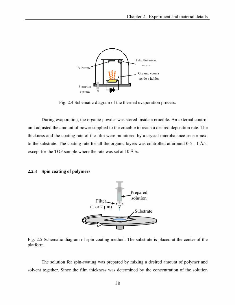
Chapter 2 - Experiment and material details
38
Fig. 2.4 Schematic diagram of the thermal evaporation process.
During evaporation, the organic powder was stored inside a crucible. An external control
unit adjusted the amount of power supplied to the crucible to reach a desired deposition rate. The
thickness and the coating rate of the film were monitored by a crystal microbalance sensor next
to the substrate. The coating rate for all the organic layers was controlled at around 0.5 - 1 Å/s,
except for the TOF sample where the rate was set at 10 Å /s.
2.2.3 Spin coating of polymers
Fig. 2.5 Schematic diagram of spin coating method. The substrate is placed at the center of the platform.
The solution for spin-coating was prepared by mixing a desired amount of polymer and
solvent together. Since the film thickness was determined by the concentration of the solution

Chapter 2 - Experiment and material details
39
and the spin rate, the weights of polymer and solvent were carefully controlled. Afterwards, the
solution was modestly warmed (below the boiling temperature of the solvent) and stirred for 12
hours to ensure the polymer was completely dissolved. The prepared solution was then dropped
on the substrate through a syringe filter to eliminate any large particles. After spin-coating, the
film was either heated or let to naturally dry inside a glove box to remove the solvent.
2.3 Characterization techniques and apparatus
2.3.1 Time-of-flight (TOF) technique
The application of TOF in organic materials was first introduced by Kepler to investigate
an anthracene crystal in 1960.[2] Since then, the technique has been widely applied not only to
crystalline, but also on many amorphous material systems. The concept of TOF is straight-
forward. As shown in Fig. 2.6, normally a sample with a thick organic film (> 3 μm) sandwiched
by two semi-transparent electrodes is prepared. This ensures the photo-generated carriers are
mostly at the interface. In order to prevent a space charge effect, non-injecting (large carrier
injection barrier) electrode is normally used. The sample is then housed inside a temperature-
regulated cryostat with the transparent electrode facing the laser source. Once it is illuminated by
a laser pulse, both free electrons and holes are generated. Depending on the polarity of the
external applied electric field (Stanford Research System, PS310), either holes or electrons will
drift through the organic layer to the counter electrode. As a result, a transient current can be
recorded by a digital oscilloscope (Agilent 54622A) through a sensing resistor.

Chapter 2 - Experiment and material details
40
Frequency-tripled Nd:YAG pulsed laser
= 355 nm pulsed width = 6 ns
Compressed He
Agilent 54622A
Cryostat at 10-7 Torr
488
Fig. 2.6 Schematic diagram of the TOF setup with an organic sample housed inside the cryostat.
A typical transient current can be divided into two main regions as shown in Fig. 2.7. The
first one is the plateau region, which corresponds to the collective motion of photo-generated
carriers, before arriving at the charge-collecting electrode. The second region is the tail region,
which arises from diffusion, or detrapping of carriers.[3] This is mostly described as the
dispersive tail. The transit time (τ ) for either holes or electrons to pass through the sample can
be determined by the turning point of the transient current. The drift velocity (ν) can be
calculated by ν = d / τ, where d is the sample thickness. According to the definition of mobility μ
= ν / F, where F represents the external applied electric field, the hole or electron mobility can be
calculated. It should be noticed that the turning point in the transient current reflects the transit
time of the fastest carrier. For DC measurements, such as current-voltage (IV), an average
mobility should be considered. From the TOF transient, the average transit time τdc can be
roughly taken as the time when the current drops to half of its plateau value.

Chapter 2 - Experiment and material details
41
Fig. 2.7 Typical photocurrent transient measured by TOF technique
The experimental results of the TOF measurements on those materials used in this study can be
found in Appendix A.
2.3.2 Admittance Spectroscopy (AS)
Fig. 2.8 Schematic diagram of the experiment setup of admittance spectroscopy

Chapter 2 - Experiment and material details
42
The first analytical model to describe the space charge effect on device admittance, Y,
was developed by J. Shao et al. in 1961.[4] They investigated the carrier dynamics in trap-free
space-charge-limited cadmium sulphide diodes. It was demonstrated that the carrier transit time
is related to the frequency-dependent admittance of the device. In 1999, H. C. F. Martens et al.
derived an equivalent admittance model and included both dispersions of carrier mobility and
transit time to describe carrier hopping in disorder polymeric solids.[5] Recently, this technique
has been proved to be consistent with the mobility measured by TOF technique.[6] Afterwards, it
has been widely studied not only on single carrier mobility, but also in the cases of bipolar
injection, trapping, dispersive transport, and carrier recombination processes in organic
electronic materials.[7-14]
The schematic diagram of the AS setup is shown in Fig. 2.8. A typical AS sample
consists of an organic layer sandwiched by two electrodes. One of the electrodes forms an Ohmic
contact, while another side should have a large injection barrier to suppress carrier injection. The
sample was housed inside a temperature-regulated cryostat. All measurements were conducted in
vacuum with a base pressure of 10-7 Torr. The admittance of the sample was evaluated by an
impedance analyzer (HP 4284A). During the measurement, a DC voltage Vdc and an AC voltage
vac were superimposed and applied to the sample. The small AC signal vac is scanned from 20 Hz
to 1 MHz with a 50 mV peak-to-peak value, and the vac has a direct influence on the carrier
relaxation processes inside the organic film. The time-scale to build-up the charge carrier is
given by the transit time τdc of the injected carrier. At low frequency (ω < τdc-1), the injected
space charges are fast enough to respond to the modulation of vac, resulting to an extra current.
Briefly, as C(ω) = Im(Y/ ω) = |Y| sin θ / ω, at high frequency, the organic layer behaves as a pure
capacitor. The phase difference between vac and iac is 90o. Once the frequency of vac drops below
the carrier transit time, the contribution of the additional current becomes significant. Eventually,
the phase difference between the additional iac and vac becomes less than 90o. Therefore, the
measured capacitance will be decreased. A typical capacitance vs frequency plot with space-
charge effect is shown in Fig. 2.9.

Chapter 2 - Experiment and material details
43
10-3 10-2 10-1 100 101 10210-3
10-2
10-1
100
Nor
mal
ized
-ΔB
Normalized frequency f * τdc
1−rτ
τdc ~ 0.56 τr
10-3 10-2 10-1 100 101 102
0.8
1.0
1.2
1.4
1.6
Nor
mal
ized
cap
acita
nce
C /
Cge
o
Normalized frequency f * τdc
Fig. 2.9 (a) The capacitance-frequency relationship can be directly measured by the impedance analyzer. (b) By definition, the negative differential suspectance –ΔB = - ω (C- Cgeo). The maximum point in the –ΔB plot corresponds to τr
-1, which is related to the average carrier transit time τdc in the TOF experiment by τdc = 0.56 τr.[6]
The effect mentioned above can be clearly observed by converting the plot of capacitance
to the negative differential susceptance –ΔB = - ω (C- Cgeo) as shown in Fig. 2.9(b). The
maximum frequency (fr or τr-1) in the –ΔB plot is found to be related to the average carrier transit
time (τdc) by τdc = 0.56 τr, where τdc is the average transit time obtained in the TOF experiment.[6]
2.3.3 Current-voltage-luminance (IVL) measurement
The setup shown in Fig. 2.10 is for measuring the I-V and L-I characteristics of OLEDs.
These two measurements are conducted simultaneously. The whole setup consists of a
programmable parameter analyzer (HP 4140B). It provides a driving voltage and captures the
response current from organic samples. Simultaneously, a luminance meter (Minolta LS-110) is
used to measure the luminance of the device.

Chapter 2 - Experiment and material details
44
Fig. 2.10 Schematic diagram of the experiment setup of IVL measurement.
2.4 Organic electronic materials used for this study
Chemical name and abbreviation Chemical structure Note
4,4’,4’’-Tris(N-3-methylphenyl-
N-phenyl-amino) triphenylamine
(MTDATA) N
N
NN
Me
Me
Me
Hole injecting material
used in OLED
N,N’-diphenyl-N,N’-bis(1-
naphthyl)(1,1’-biphenyl)-
4,4’diamine
(NPB)
N N
Hole transporting
material used in OLED
N,N’-diphenyl-N,N’-bis(3-
methylphenyl)(1,1’-biphenyl)-
4,4’diamine
(TPD)
N NH3C CH3
Hole transporting
material used in OLED
Copper Phthalocyanine
(CuPc)
Hole injecting material
used in OLED
Electron donor in OPV
p-type material in OFET

Chapter 2 - Experiment and material details
45
4,4’,4’’-tris(N-carbazolyl)-
triphenylamine
(TCTA)
N
N
NN
Hole transporting
material
Host material for electro-
phosphorescent OLED
Mes2B(p-4,4´-biphenyl-NPh(1-
naphthyl))
(BNPB) N B
Blue emitting material
used in OLED
Aluminum tris(8-
hydroxyquinoline)
(Alq3) O
O
OAl
N
NN
Green emitting material
used in OLED
2,2',2''-(1,3,5-phenylene) tris(1-
phenyl-1H-benzimidazole)
(TPBI)
Electron transporting and
hole blocking material
used in OLED
tetra-
fluorotetracyanoquinodimethane
(F4- TCNQ)
CCN
CNC
NC
NC
FF
FF p-type dopant
Fullerene
(C60)
Electron acceptor used in
OPV
n-type material used in
OFET
Poly(3-hexylthiophene)
(P3HT)
Electron donor used in
OPV
[6,6]-Pentadeuterophenyl C61
butyric acid methyl ester
(PCBM)
Electron acceptor used in
OPV

Chapter 2 - Experiment and material details
46
References
[1] M. G. Mason, L. S. Hung, C. W. Tang, S. T. Lee, K. W. Wong, and M. Wang, J. Appl.
Phys. 86, 1688 (1999).
[2] R. G. Kepler, Phys. Rev. 119, 1226 (1960).
[3] W. Warta, R. Stehel, and N. Karl, Appl. Phys. A 36, 163 (1985).
[4] J. Shao and G. T. Wright, Solid-State Electro. 3, 291 (1961).
[5] H. C. F. Martens, H. B. Brom, and P. W. M. Blom, Phys. Rev. B 60, R8489 (1999).
[6] S. W. Tsang, S. K. So, and J. B. Xu, J. Appl. Phys. 99, 013706 (2006).
[7] Stefan Berleb and Wolfgang Brütting, Phys. Rev. Lett. 89, 286601 (2002).
[8] S. W. Tsang, S. C. Tse, K. L. Tong, and S. K. So, Org. Electron. 7, 474 (2006).
[9] S. W. Tsang, K. L. Tong, S. C. Tse, and S. K. So, Proc. SPIE 6333, 633313 (2006).
[10] D. Poplavskyy and F. So, J. Appl. Phys. 99, 033707 (2006).
[11] E. Ehrenfreund, C. Lungenschmied, G. Dennler, H. Neugebauer, and N. S. Sariciftci,
Appl. Phys. Lett. 91, 012112 (2007).
[12] M. Schmeits, J. Appl. Phys. 101, 084508 (2007).
[13] N. D. Nguyen, M. Schmeits, and H. P. Loebl, Phys. Rev. B 75, 075307 (2007).
[14] K. L. Tong, S. W. Tsang, K. K. Tsung, S. C. Tse, and S. K. So, J. Appl. Phys. 102,
093705 (2007).

47
Chapter 3 Chargecarrier induced barrierheight reduction at organic
heterojunction
3.1 Abstract
In order to provide an accurate theoretical description of current density – voltage (J-V)
characteristics of an organic heterojunction device over a wide range of electric fields at various
temperatures, it is proposed that an accumulation of charge carriers at the heterojunction will
lead to a reduction in the barrier height across the heterojunction. Two well-known hole
transporting materials, 4,4’,4’’-Tris(N-3-methylphenyl-N-phenyl-amino) triphenylamine
(MTDATA) and N,N’-diphenyl-N,N’-bis(1-naphthyl)(1,1’-biphenyl)-4,4’diamine (NPB) were
used to fabricate an unipolar heterojunction device. It is found that the J–V characteristics
depends strongly on applied bias. The simulated J-V characteristics of the heterojunction device,
with the modified injection model, are found to be in excellent agreement with the experimental
data.

Chapter 3 - Charge-carrier induced barrier-height reduction at organic heterojunction
48
3.2 Introduction
Heterojunctions formed by two semiconductors have been the foundational technology
for many modern electronic devices since 1950s.[1] The first high efficiency organic light-
emitting-diode (OLED) structure based on a stack of multi-layer organic materials[2] has become
a standard device platform in commercial production. Recently, 5% power conversion efficiency
from organic photovoltaic (OPV) cells has been demonstrated in small-molecule heterojunction
devices and in polymeric blend structures,[3,4] and thus low cost OPV cells with current printing
technology become commercially attractive. Despite those technological achievements with the
applications of organic heterojunctions, the studies and understanding of the physics of the
charge injection process across organic heterojunction are still very limited. [5-8]
There are two key factors that control the injection current at a heterojunction. One is the
energy level alignment which determines the barrier height. According to recently reported
photoemission studies, the interface alignment between two undoped organic materials often
agrees with the vacuum level alignment rule. However, when one side of the heterojunction has
extrinsic carriers, introduced either by chemical doping or electrical doping due to charge carrier
accumulation, a considerable re-alignment of energy levels at the interface has been observed.[9-
12] We have also reported that the injection current across an organic heterojunction device can
be tuned by inserting a thin 2 nm chemically-doped interlayer with different doping
concentrations at the interface.[13] The other factor is the nature of the charge injection process. It
is generally believed that the charge transport in organic materials is governed by the Miller-
Abrahams type hopping process between localized transporting sites.[14]
Recently, Arkhipov et al. have proposed a two step hopping model to describe the charge
carrier transport across an interface of disordered organic dielectric.[5] The injection model
considers the jump rate of a carrier from the center of the Gaussian density-of-state (DOS) in the
injecting layer into the DOS of the accepting layer. However, the model does not include the
energy distribution and occupation of carriers at the interface. Moreover, the calculated field
dependence of the injection current is much smaller than those observed experimentally, as
depicted in Fig. 3.1. Woudenbergh et al. found that measurements of a polymeric heterojunction

Chapter 3 - Charge-carrier induced barrier-height reduction at organic heterojunction
49
device do not match the injection model.[6] They modified the model to account for the charge
filling effect of holes in the injecting layer by assuming the carriers are injected from the quasi-
Fermi level rather than from the center of the highest-occupied-molecular orbital (HOMO).
1 1010-10
10-9
10-8
10-7
10-6
10-5
10-4
10-3
10-2
J (A
/cm
2 )
Voltage (V)
Arkhipov's model
measured
T = 288 K
Fig. 3.1 Comparison between (line) previous injection model and (symbols) the measured current density of a two-layer device.
In this chapter, systematic experimental current density – voltage (J-V) characteristics of
organic heterojunction devices made from relatively well-understood organic molecules were
studied. In order to describe the experimental results, we found that it is essential to include two
critical parameters to the existing theory: a) energy distribution of carriers at the injecting layer
interface, and b) dynamic barrier height, vφ , associated with quasi-Fermi level shifting.

Chapter 3 - Charge-carrier induced barrier-height reduction at organic heterojunction
50
3.3 Experiment
The approach in this experiment is to use a unipolar device where the current is mainly
determined by the charge injection process at the organic heterojunction. This requires that the
contact resistance at the metal-organic (MO) interface for charge injection and the number of
trap states in the bulk organic material are negligible. This can be achieved by using 4,4’,4’’-
Tris(N-3-methylphenyl-N-phenyl-amino) triphenylamine (MTDATA) and N,N’-diphenyl-N,N’-
bis(1-naphthyl)(1,1’-biphenyl)-4,4’diamine (NPB) to fabricate the heterojunction device.
MTDATA and NPB are prototypical hole-injecting and hole-transporting materials used in
OLED technology. The amorphous films formed with MTDATA and NPB provide a smooth
surface that can effectively prevent any effect of non-homogeneous electric field at the OOI from
a rough surface. The surface topology of MTDATA on ITO obtained by AFM is shown in Fig.
3.2.
Fig. 3.2 Surface topology of 320 nm MTDATA obtained by AFM with surface roughness (rms) equal to 0.9 nm.
Due to the difference in HOMO levels of MTDATA (5.0-5.1 eV) and NPB (5.4-5.6 eV),[10,11,15]
there exists an energy barrier of around 0.5 eV for hole injection at the MTDATA / NPB
interface. It has also been demonstrated that an quasi-Ohmic contact is formed at the indium tin

Chapter 3 - Charge-carrier induced barrier-height reduction at organic heterojunction
51
oxide (ITO) and MTDATA interface.[13,16] Moreover, the trap-free space-charge-limited
conduction behavior in single layer devices supports that there are a negligible number of trap
states in both materials.[13,16,17]
A hole-only heterojunction device with a structure of anode / injecting layer / accepting
layer / cathode was fabricated for this study. Pre-patterned ITO coated glass substrate was used
as the anode. The substrate was cleaned by a sequence of ultrasonic solvent baths and followed
by UV-ozone treatment. A 320 nm layer of MTDATA was thermally evaporated on top of ITO
as the injecting layer. It was then covered by 390 nm of thermally evaporated NPB as the
accepting layer. Finally, silver was evaporated on top of NPB to form the cathode. The organic
and metal layers were fabricated in a single vacuum system with a base pressure of 10-8 Torr. On
the cathode side, a large energy difference between the lowest unoccupied molecular orbital
(LUMO) of NPB (2.5 eV) and the work function of Ag (4.3 eV) effectively restricts electron
injection into the device. The field and temperature dependent hole mobilities of individual
organic material were characterized by the time-of-flight (TOF) technique. Details of TOF
measurement has been described in the Experimental section. The measured mobilities were
fitted to the Gaussian-disordered model (GDM),[18] the extracted parameters are listed in
Appendix A.
3.4 Results and discussion
3.4.1 Steady-state simulation: extracting Fint and pint
In order to compare the injection model to the measured J-V characteristics of an
heterojunction device, the electric field at the interface, Fint, and the charge carrier densities at
both sides of the interface region, the injecting layer side, pint1, and the accepting layer side, pint2,
have to be determined. The complete two layer organic system including contacts was modeled
using ATLAS,[19] to solve the standard electric field, drift, and diffusion equations used in
semiconductor modeling. The iteration method was similar to the method used in Ref. [6]. The

Chapter 3 - Charge-carrier induced barrier-height reduction at organic heterojunction
52
applied voltages and measured current densities were used as the input parameters to a steady-
state model of the device. The field and temperature dependent mobilities measured by TOF
were used in the simulation. The hole-injecting electrode was modeled using a Schottky contact
with the barrier height chosen to give a density of holes equal to 1021 cm-3 at the anode / injecting
layer interface. The cathode / accepting layer interface was specified as Ohmic (i.e. the hole
concentration is pinned to the equilibrium value at this contact). ATLAS does not contain the
hopping injection model. Instead, we used a thermal injection model at the organic
heterojunction and adjusted the parameters to give our measured current for each applied
voltage. This is equivalent to modeling the two layers separately and using the current and
electric field as boundary conditions at the interface. The simulation procedure is illustrated in
Fig. 3.3.
Fig. 3.3 Simulation procedure with ATLAS for a two-layer system to extract the electric field and carrier distributions.

Chapter 3 - Charge-carrier induced barrier-height reduction at organic heterojunction
53
As shown in Fig. 3.4, the results of the simulation show that the holes pile up at the
injecting layer side of the interface creating a large electric field, which remains constant across
the accepting layer. In the range of applied voltage considered here, there is a low and constant
concentration of holes throughput the accepting layer. The current in the accepting layer is
simply given by int2int FpeJ μ≈ .
0.2
0.4
0.6
-5 -4 -3 -2 -1 0 1 2 3 4 5108
1010
1012
1014
1016
1018
1020
(b)
F (M
V/c
m) (a)
Distance away from interface x (nm)
accepting layer
Applied voltage (V) 25 21 17 13 9 5
p (c
m-3)
T = 288 K
injecting layer
Fig. 3.4 Extracted (a) electric field and (b) carrier distribution near the OOI.
Re-plotting Fig. 3.4, the interface electric field and carrier density can be obtained as shown in
Fig. 3.5 and Fig. 3.6 respectively. Fint is linearly proportional to the applied voltage. Since the
energy offset at the MTDATA / NPB interface effectively suppresses hole injection, the hole
density in MTDATA is much higher then that in NPB as depicted in Fig. 3.6. As a result, most of
the applied voltage drops across the NPB film. The electric fields at the OOI and across the TPD
film are only slightly less than directly calculated from V / dNPB. Moreover, both Fint and pint are

Chapter 3 - Charge-carrier induced barrier-height reduction at organic heterojunction
54
independent of temperature, as mentioned in Ref.[6] , the charge distribution in the injecting
layer MTDATA is governed by electrostatics. Even though the injection current at the OOI is
smaller at lower temperature, a much higher carrier density in the injecting layer makes the
electric field mostly distributed in the accepting layer.
0 5 10 15 20 25 300.0
0.1
0.2
0.3
0.4
0.5
0.6
0.7
Temperature (K) 323 288 266 219 172
F int (M
V/c
m)
Voltage (V)
Fig. 3.5 Extracted interface electric field Fint with ATLAS at different temperatures.

Chapter 3 - Charge-carrier induced barrier-height reduction at organic heterojunction
55
0.0 0.1 0.2 0.3 0.4 0.5 0.6 0.7108
1010
1012
1014
1016
1018
1020
pint2Temperature (K)
323 288 266 219 172
p int (c
m-3)
Fint (M V/cm)
pint1
Fig. 3.6 Extracted carrier density at the injecting (first) layer side of the interface, pint1, and the accepting (second) layer side of the interface, pint2, with ATLAS.
3.4.2 Modified injection model at OOI
We have modified the injection model to account for the hole occupation by summing the
contribution to the current of all the occupied hole states, ( )Ep 1int , at the injecting layer side of
the interface:

Chapter 3 - Charge-carrier induced barrier-height reduction at organic heterojunction
56
( ) ( ) ( )
( ) ]esc
at
wEg
xeFEEBoldExdxeN
EpdEJ
2int
int2int1int2int01int1int
1int 2exp
×
⎢⎣⎡ −+−−= ∫ ∫ ∫
∞
∞−
∞ ∞
∞−φγν
(3.1)
where Nt is the total DOS, e is the electron charge, v0 is the attempt-to-jump frequency of the
order of the phonon frequency, Eint1 is the energy of carriers at the injecting layer side of the
interface , a is the nearest-neighbor distance, γ is the inverse localization radius, and x is the
hopping distance into the accepting layer. Eint2 is the energy of the first site on the accepting side,
φ is the barrier height, Fint is the interface electric field, ( ) ( )22 2/exp2/ σσπ ENEg t −= is the
Gaussian DOS in the accepting layer, and Bol(E) is the energy dependence of the jump rate:
( ) ( )⎩⎨⎧
>−<
=0/exp01
EkTEE
EBol
(3.2)
The expression inside the square bracket in Eq. (3.1), without the term Eint1, was derived by
Arkhipov et al. .[5] It calculates the thermally assisted hopping rate for a hole at the interface of
the injecting layer to a site over a distance, x, into the accepting layer. This is multiplied by the
escape probability, wesc, of the hole continuing into the bulk of the accepting layer (as opposed to
hopping back down the barrier). The expression from Ref. [5] assumes that there is a hole, at the
HOMO level of the interface of the injecting layer, for every receiving site in the accepting layer.
Our modification accounts for the occupancy and the energy distribution of holes at the injecting
layer side of the interface. In order to do this, the expression in the square bracket is multiplied
by the probability that an injecting site is occupied, pint1(E)/Nt, and everything is integrated over
Eint1. The argument of Bol(E) was modified from (φ + Eint2 –eFintx) in Ref. [5] to (φ – Eint1 + Eint2
–eFintx) to account for the energy distribution in the injecting layer.

Chapter 3 - Charge-carrier induced barrier-height reduction at organic heterojunction
57
Using the ATLAS simulation results for 1intp , the quasi-Fermi level FE and the hole
occupation probability ( )Ep 1int can be obtained using:
( ) ∫∫∞
∞−
∞
∞−
⎟⎠⎞
⎜⎝⎛ −
+
⎟⎟⎠
⎞⎜⎜⎝
⎛⎟⎠⎞
⎜⎝⎛−
==
kTEE
E
dENEpdEpF
t
exp1
2/1exp
2
2
1int1int
σ
σπ
(3.3)
where σ is the width of the Gaussian DOS in the injecting layer. ( )1int1int Ep and the integrand of
Eq. (3.1), )( 1intEJ , are plotted as a function of Eint1 in Fig. 3.7 for different values of FE .
0.0
0.2
0.4
0.6
0.8
1.0
-0.6 -0.4 -0.2 0.0 0.2 0.4
0.0
0.2
0.4
0.6
0.8
1.0 (b)
p int1 (E
int1)
-0.2 -0.3 -0.4
EF (eV) (a)
J (E
int1)
Eint1 (eV)
Fig. 3.7 (a) The normalized Gaussian energetic distribution of the carrier density pint1(Eint1) at the injecting layer side of the interface. (b) The normalized factional injection current densities J(Eint1) contributed by the carriers at different energy levels. The results are compared with different values of the quasi-Fermi level EF (from -0.2 eV to -0.4 eV).
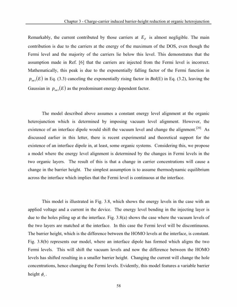
Chapter 3 - Charge-carrier induced barrier-height reduction at organic heterojunction
58
Remarkably, the current contributed by those carriers at FE is almost negligible. The main
contribution is due to the carriers at the energy of the maximum of the DOS, even though the
Fermi level and the majority of the carriers lie below this level. This demonstrates that the
assumption made in Ref. [6] that the carriers are injected from the Fermi level is incorrect.
Mathematically, this peak is due to the exponentially falling factor of the Fermi function in
( )Ep 1int in Eq. (3.3) canceling the exponentially rising factor in Bol(E) in Eq. (3.2), leaving the
Gaussian in ( )Ep 1int as the predominant energy dependent factor.
The model described above assumes a constant energy level alignment at the organic
heterojunction which is determined by imposing vacuum level alignment. However, the
existence of an interface dipole would shift the vacuum level and change the alignment.[20] As
discussed earlier in this letter, there is recent experimental and theoretical support for the
existence of an interface dipole in, at least, some organic systems. Considering this, we propose
a model where the energy level alignment is determined by the changes in Fermi levels in the
two organic layers. The result of this is that a change in carrier concentrations will cause a
change in the barrier height. The simplest assumption is to assume thermodynamic equilibrium
across the interface which implies that the Fermi level is continuous at the interface.
This model is illustrated in Fig. 3.8, which shows the energy levels in the case with an
applied voltage and a current in the device. The energy level bending in the injecting layer is
due to the holes piling up at the interface. Fig. 3.8(a) shows the case where the vacuum levels of
the two layers are matched at the interface. In this case the Fermi level will be discontinuous.
The barrier height, which is the difference between the HOMO levels at the interface, is constant.
Fig. 3.8(b) represents our model, where an interface dipole has formed which aligns the two
Fermi levels. This will shift the vacuum levels and now the difference between the HOMO
levels has shifted resulting in a smaller barrier height. Changing the current will change the hole
concentrations, hence changing the Fermi levels. Evidently, this model features a variable barrier
height vφ .

Chapter 3 - Charge-carrier induced barrier-height reduction at organic heterojunction
59
Fig. 3.8 Schematic diagrams of energy level alignment at the heterojunction with the boundary condition of (a) vacuum level alignment and (b) Fermi level alignment. The lower graphs are the corresponding alignment of the Gaussian density-of-state (DOS) at both sides of the interface. The shaded region represents those states occupied by electrons.

Chapter 3 - Charge-carrier induced barrier-height reduction at organic heterojunction
60
3.4.3 Comparison with experiment
Using Eq. (3.3) and the simulated interface hole densities 1intp and 2intp of the ITO /
MTDATA (320 nm) / NPB (390 nm) / Ag heterojunction device, the variable barrier vφ can be
obtained by adjusting the energy alignment so that the Fermi levels FE match at the
MTDATA/NPB interface. Our choice of the values of MTDATAσ and NPBσ used in the calculation
will be discussed later. Fig. 3.9 shows the calculated vφ as a function of applied voltage at
different temperatures. vφ varies little with temperature, but it decreases exponentially when the
applied voltage increases. This can be explained by the occupancy of holes in the interface
DOSs. According to the simulation results, with increasing voltage, 1intp increases from 1017 cm-
3 to 1019 cm-3 and 2intp increases from 109 cm-3 to 1013 cm-3. The amount of change of the Fermi
levels depends on the changes in 1intp and 2intp and on the DOS (at the position of the Fermi
levels). In this device the Fermi level in the accepting layer changes more rapidly than that in the
injecting layer, leading to a decreasing barrier as voltage increases. It can be deduced that,
besides the energy difference of the HOMO levels, the energy profile is significant in controlling
carrier injection across organic heterojunction.

Chapter 3 - Charge-carrier induced barrier-height reduction at organic heterojunction
61
0.1 0.2 0.3 0.4 0.5 0.6 0.7
0.45
0.50
0.55
0.60
0.65
5 10 15 20 25 30
Fint (M V/cm)
Voltage (V)
Temperature (K) 323 288 266 219 172
φ v (eV
)
Fig. 3.9 The field and voltage dependence of the variable barrier vφ at 323 K ( ), 288 K ( ), 266 K ( ), 219 K ( ), and 172 K ( ). Assuming thermodynamic equilibrium, vφ is calculated by Eq. (4) with 1intp and 2intp obtained by the steady-state simulation. The solid line is a fitting curve to an exponential decay function.
The inset in Fig. 3.10 illustrates the first step in our calculation for the ITO / MTDATA /
NPB / Ag heterojunction device. An inverse localization radius γ = 5 x 107 cm-1 has been
used.[21] The nearest-neighbor distance a = 1 nm is taken as the size of a NPB molecule. By
assuming only one net charge is carried by a molecule at a given time, the total number of DOS
Nt ≈ 1 x 1021 cm-3. For a fixed interface electric field (Fint = 0.5 M V/cm), the disorder
parameters MTDATAσ and NPBσ , and the attempt-to-jump frequency, 0ν are varied to obtain the
best fit to the temperature dependent data. Using the values 0ν = 7.88 x 10¹³ s-1, vφ = 0.45 ± 0.1
eV, MTDATAσ = 95 meV and NPBσ = 110 meV, the theory agrees with the observed thermally
activated current. The values for the disorder are slightly larger than those obtained from TOF

Chapter 3 - Charge-carrier induced barrier-height reduction at organic heterojunction
62
measurement. A broadening would be expected in the presence of an interface dipole.[22] The
above values are used in Eq. (3.1) with the introduction of the variable barrier, vφ , to calculate
the J vs Fint characteristics in Fig. 3.10. The calculated electric field and temperature dependent
injection current densities are in excellent agreement with the experimental results. The good
agreement between two sweeping directions of the applied voltage at all temperatures also
suggests that the trap charging effect is negligible. It is worthwhile noting that ignoring the
contribution of the variable barrier vφ will vastly underestimate the field dependence of the
injection current across the heterojunction.
105 10610-9
10-8
10-7
10-6
10-5
10-4
10-3
10-2
3 4 5 6
10-7
10-6
10-5
10-4
10-3
J (A
/cm
2 )
1000/T (K-1)
Fint = 0.5 M V/cm
172K
219K
266K
288K
J (A
/cm
2 )
Fint (V/cm)
323K
opened symbols (measured)closed symbols (calculated)
Fig. 3.10 Measured J - Fint characteristics of the ITO / MTDATA(320 nm) / NPB(390 nm) / Ag heterojunction device at 323 K ( ), 288 K ( ), 266 K ( ), 219 K ( ), and 172 K ( ). The corresponding solid symbols are the calculation results based on the modified injection model in Eq. (3) with the variable barriers vφ in Fig. (3). The inset is the J vs 1/T plot at Fint = 0.5 M V/cm.

Chapter 3 - Charge-carrier induced barrier-height reduction at organic heterojunction
63
Fitting the calculation results (solid line) with Eq. (3) to the experiment results (opened symbols) obtains vφ = 0.45 ± 0.1 eV, MTDATAσ = 95 meV and NPBσ = 110 meV.
3.5 Conclusion
In conclusion, an injection model for an organic heterojunction which includes the
distribution of carriers at the injecting side of the interface has been proposed. This model shows
that the main contribution to the injection current is from carriers at the peak of the Gaussian
density-of-state (DOS) rather than at the Fermi level. In addition, we have proposed a variable
injection barrier height vφ which arises from the energy level re-alignment triggered by the
relative Fermi level shifting caused by charge carrier accumulation at the interface. The model is
verified by the excellent agreement with the experimental results of the current density – voltage
(J-V) characteristics of an organic heterojunction device for various temperatures over a wide
range of electrical field. The results show that a dynamic change in carrier concentration and
DOS energy alignment at the heterojunction plays a significant role in the performance of
organic heterojunction devices.

Chapter 3 - Charge-carrier induced barrier-height reduction at organic heterojunction
64
3.6 References
[1] W. Shockley, U. S. (1951).
[2] C. W. Tang and S. A. VanSlyke, Appl. Phys. Lett. 51, 913 (1987).
[3] J. Xue, S. Uchida, B. P. Rand, and S. R. Forrest, Appl. Phys. Lett. 85, 5757 (2004).
[4] J. Peet, J. Y. Kim, N. E. Coates, W. L. Ma, D. Moses, A. J. Heeger, and G. C. Bazan,
Nature Mater. 6, 497 (2007).
[5] V. I. Arkhipov, E. V. Emelianova, and H. Bassler, J. Appl. Phys. 90, 2352 (2001).
[6] T. v. Woudenbergh, J. Wildeman, and P. W. M. Blom, Phys. Rev. B 71, 205216 (2005).
[7] H. Houili, E. Tutis, I. Batistic, and L. Zuppiroli, J. Appl. Phys. 100, 033702 (2006).
[8] S. W. Tsang, M. W. Denhoff, Y. Tao, and Z. H. Lu, Phys. Rev. B 78, 081301 (2008).
[9] H. Vazquez, W. Gao, F. Flores, and A. Kahn, Phys. Rev. B 71, 041306 (2005).
[10] A. Kahn, W. Zhao, W. Gao, H. Vázquez, and F. Flores, Chem. Phys. 325, 129 (2006).
[11] J. X. Tang, C. S. Lee, and S. T. Lee, J. Appl. Phys. 101, 064504 (2007).
[12] S. Braun, W. Osikowicz, Y. Wang, and W. R. Salaneck, Org. Electron. 8, 14 (2007).
[13] S. W. Tsang, Z. H. Lu, and Y. Tao, Appl. Phys. Lett. 90, 132115 (2007).
[14] A. Miller and E. Abrahams, Phys. Rev. 120, 745 (1960).
[15] Y. Shirota, T. Kobata, and N. Noma, Chem. Lett. 18, 1145 (1989).
[16] G. Carsten, A. Homer, D. C. B. Donal, and S. Yasuhiko, Appl. Phys. Lett. 72, 2448
(1998).
[17] S. W. Tsang, S. C. Tse, K. L. Tong, and S. K. So, Org. Electron. 7, 474 (2006).
[18] H. Bässler, Phys. Status Solidi B 175, 15 (1993).
[19] ATLAS, ATLAS device simulation software (SILVACO, Santa Clara).
[20] H. Ishii, K. Sugiyama, E. Ito, and K. Seki, Adv. Mater. 11, 605 (1999).
[21] E. L. Wolf, Principle of Electron Tunneling Spectroscopy. (Oxford University Press,
New York, 1995).
[22] M. A. Baldo and S. R. Forrest, Phys. Rev. B 64, 085201 (2001).

65
Chapter 4 Temperature dependence of carrier injection across organic
heterojunctions
4.1Abstract
Theoretical and experimental study of carrier injection across organic heterojunctions of various
barrier heights (0.4 eV – 1.0 eV) over a wide range of temperatures is presented in this chapter.
An injection model with proposed escape probability function wesc is formulated to include the
total hopping frequency at both sides of the heterojunction. The model predicts that the injection
current at low temperature can be dramatically modified by an extremely small amount of deep
trap states. Moreover, the temperature dependence of the injection current is found to decrease
with increasing barrier height. This suggests that extracting the barrier height from the J vs 1/T
plot, as commonly employed in literature, is problematic. Experimentally, heterojunction
devices with injection barrier from 0.4 eV to 1.0 eV are fabricated from various organic
materials. The measured temperature dependence of the injection current is in good agreement
with the calculated results. By measuring the carrier mobility of a single layer device at low
temperature, a temperature dependence similar to the heterojunction devices suggests that the
small density of deep trap states originates in the bulk of the material.

Chapter 4 - Temperature dependence of carrier injection across organic heterojunctions
66
4.2 Introduction
As discussed in Chapter 3, owing to the weak coherence of electronic states in disordered
organic materials, the carrier injection across organic heterojunctions is treated as a hopping or
thermally assisted tunneling process. The hopping rate v of a carrier being injected from a
starting site to a target site, separated by a distance x and with energy difference E, can be simply
described by the Miller-Abrahams expression:[1]
( ) ( )Ex Bol2exp0 γνν −= (4.1)
( ) ( )⎩⎨⎧
>−<
=0/exp01
BolEkTEE
E (4.2)
where v0 is the attempt-to-jump frequency having a value close to the phonon frequency, γ is the
inverse localization radius, and Bol(E) accounts for the energy independent downward (E < 0)
and energy dependent upward (E > 0) jumps.
Fig. 4.1 illustrates the injection of carriers across an organic heterojunction. The injection
process can be basically divided into two steps: 1) In order to overcome the energy barrier φ,
carrier injection into the density-of-state (DOS) of the second layer is accomplished by an
upward jump. 2) After a carrier is injected into the second layer, it will either jump back into the
first layer or further advance to the bulk of the second layer. This process is described by the
escape probability wesc of the injected carrier. Due to the exponential dependence of the
thermionic process, it can be easily deduced that the injection current is largely depended on the
shape of the DOS at both sides of the interface. Under thermodynamic equilibrium condition,
those carriers that accumulate at the first layer side of the interface will fill up the lower energy

Chapter 4 - Temperature dependence of carrier injection across organic heterojunctions
67
states. As a result, a broader DOS in the first layer will eventually reduce the injection current.
On the other hand, a broader DOS in the second layer has more low energy states that facilitates
the injection. The impact of accumulated charges at organic-organic interface (OOI) on carrier
injection has been discussed in Chapter 3. Moreover, since the downward jump is energetically
favorable as indicated in Eq. (4.2), any deep trap states in the second layer, with energy close to
or lower than the accumulated carriers in the first layer, will significantly increase the injection
current. Intuitively, the escape probability wesc of an injected charge, hopping into the bulk of the
second layer, depends on the hopping rate and the number of available sites at both sides of the
interface. This process is crucial as it determines the net injection current across the interface.

Chapter 4 - Temperature dependence of carrier injection across organic heterojunctions
68
Fig. 4.1 Illustration of carrier hopping across a disordered organic heterojunction. The density-of-state (DOS) of the lowest-unoccupied molecular orbital (LUMO) and deep trap energy levels is assumed to be Gaussian.
This chapter is organized as follow: Sec. 4.3 gives a formalism of an injection model with
a proposed wesc. Using the modified model, we calculate the impact of deep trap states on the
temperature and field dependence of the injection current. In Sec. 4.4, experiment results of a
series of heterojunction devices with barrier heights from 0.4 eV to 1.0 eV are given. The
reduced temperature dependence of injection current for larger barrier is compared to the
proposed model with deep trap states. In Sec. 4.5 we demonstrate the temperature dependence of
carrier mobility in a single layer device. The results support that the deep traps originate in the
bulk of the material with a density comparable to the model prediction. It is then followed by the
discussion and conclusion.

Chapter 4 - Temperature dependence of carrier injection across organic heterojunctions
69
4.3 Theoretical modeling
4.3.1 Carrier injection model with proposed wesc
In disordered organic materials, it is commonly assumed that the DOS has a Gaussian
distribution:
( ) ⎟⎟⎠
⎞⎜⎜⎝
⎛−= 2
2
2exp
2 σσπENEg
(4.3)
where E is the site energy reference to the center of the Gaussian DOS, N is the total DOS, and σ
is the Gaussian width. In the absence of polaronic effects, the hopping rate across the
heterojunction can be described by Eqs. (4.1) and (4.2). As discussed in Chapter 3, taking into
account the distribution of carriers ( )Ep1 at the first layer side of the interface, the injection
current J can be formulated as:[2]
( ) ( ) ( )
( ) ( )22
int2121
1110
,
2exp
ExwEg
xeFEEBoldExdxN
EpdEeJ
esc
a
×
−+−−= ∫ ∫ ∫∞
∞−
∞ ∞
∞−φγν
(4.4)
where e is the electron charge, a is the nearest-hopping distance, x is the hopping distance into
the second layer, φ is the barrier height, and Fint is the interface electric field. The first integral in
Eq. (3) describes the probability that an injecting site in the first layer is occupied. The second
and third integrals account for the hopping rate over a distance, x, of a carrier in E1 in the first

Chapter 4 - Temperature dependence of carrier injection across organic heterojunctions
70
layer into E2 in the second layer. The hopping rate is then multiplied by the DOS, ( )Eg , in the
second layer and the escape probability, ( )Exwesc , , of the carrier continuing into the bulk.
Arkhipov et al. suggest that wesc can be determined by the average number of injection-
facilitating neighbors, ( )Exni , , in the second layer.[3] The backward jump into the first layer is
assumed energetically downward. By considering the argument inside the exponential function
in Eq. (1), the backward hopping parameter is simply equal to xγ2 for a carrier localized in a site
with energy E at a distance x from the interface in the second layer. Therefore, one can calculate
( )Exni , by counting the hopping sites in the second layer with hopping parameter less than xγ2 :
( ) ( ) ( )2
2
2
1
00
2 int2, EgdEdzrdrExnzreFrxkTEx
i ∫∫∫+−+
∞−=
γπ
(4.5)
where r is the distance away from the injected carrier in the second layer, θcos=z , and θ is the
angle between the Fint and the hopping direction. The escape probability wesc is defined as the
probability that the carrier in the second layer has at least one injection-facilitating neighbor,
which is determined by the Poisson distribution:
( ) ( )[ ]ExnExw iesc ,exp1, −−= (4.6)
It is worth nothing that Eq. (4.5) is formulated by assuming all the backward jumps into the first
layer are energetically downward. Therefore, the probability in Eq. (4.6) is independent of the
barrier height φ, and is solely depended on the number of injection-facilitating neighbors in the
second layer. Fig. 3 shows the energy dependence of ( )Eawesc , of a carrier localized at a = 10-7

Chapter 4 - Temperature dependence of carrier injection across organic heterojunctions
71
cm from the interface with Fint = 5 x 10⁵ V/cm. For an injected carrier localized well above E =
0, the center of the Gaussian DOS, ( )Eawesc , saturates at 1. Because of the dramatic decreases of
the DOS in the Gaussian tail, ( )Eawesc , decreases rapidly for those carriers localized in lower
energy states. However, if the carrier is localized well below E = 0, the backward jump into the
first layer is not necessarily downward, and the number of available backward hopping sites is
also reduced. Therefore, assuming all backward jumps are downward will underestimate the
escape probability of those carriers localized in lower energy states.
We formulate the escape probability by comparing the total hopping frequency at both
sides of the interface. For an injected carrier in the second layer, a successful hop into the
neighboring site depends on both the hopping frequency, Eqs. (4.1) and (4.2), and the number of
available sites, Eq. (4.3). The escape probability is determined by the ratio of the total forward to
the overall hopping frequencies at both sides of the interface. Considering a carrier localized at a
site in the second layer with energy E and a distance x away from the interface, the total forward
hopping frequency fwν is:
( ) ( ) ( ) ( )2int22
1
00
2 Bol2exp2, EgErzeFEdEdzrrdrExfw −−−= ∫∫∫∞
∞−
∞γπν
(4.7)
and total backward hopping frequency bwν becomes:
( ) ( ) ( ) ( )1int11
1
0Bol2exp)(2, EgExzeFEdEdzrxrrdrEx
xbw −+−−−= ∫∫∫∞
∞−
∞φγπν
(4.8)
The spatial integrations of Eqs. (4.7) and (4.8) are illustrated in Fig. 4.2.

Chapter 4 - Temperature dependence of carrier injection across organic heterojunctions
72
Fig. 4.2 A schematic diagram of the spatial integration in Eqs. (4.7) and (4.8). An injected carrier at the center of the sphere is localized at a distance x away from the interface. The preferable hopping neighbors are located at a distance r from the injected carrier with a direction θ between the interface electric field.
Since most of the electric field is distributed in the second layer, the contribution of the
electric field on the potential landscape in the first layer is neglected. Using Eqs. (4.7) and (4.8),
the escape probability ( )Exwesc , is obtained:

Chapter 4 - Temperature dependence of carrier injection across organic heterojunctions
73
( )bwfw
fwesc Exw
ννν
+=,
(4.9)
As shown in Fig. 4.3, the calculated ( )Exwesc , using Eq. (4.9) approaches 1 when E is close to -
0.25 eV. Although, backward jumps for carriers localized in higher energy states are mostly
downward, the number of available sites in the second layer with a smaller hopping distance is
higher than that in the first layer. Consequently, fwν is higher than bwν even for a carrier
localized slightly below the maximum of the Gaussian DOS. On the other hand, at lower energy,
( )Exwesc , calculated with Eq. (4.9) is much larger than the one calculated with Eq. (4.6), and it
saturates to a constant value ( )kTxwesc /2exp φγ −≈ . Despite the hopping rate is higher for
downward jump, the steep increase of the Gaussian DOS from the tail to the maximum region
overwhelms the exponential decrease of the upward hopping rate. Therefore, for an injected
carrier localized well below the DOS, an upward jump into both sides of the interface is
favorable. The ratio of the forward and backward hopping rates is determined by the position of
the injected carrier, x, and the energy difference of the DOS, φ, of the first and the second layers.

Chapter 4 - Temperature dependence of carrier injection across organic heterojunctions
74
-1.5 -1.0 -0.5 0.0 0.5 1.010-16
10-14
10-12
10-10
10-8
10-6
10-4
10-2
100
-1.5 -1.0 -0.5 0.0 0.5 1.0
0.0
0.2
0.4
0.6
0.8
1.0
Eq. (4.9)
wes
c
E (eV)
Eq. (4.6)
Fig. 4.3 Calculated escape probability function wesc using Eq. (4.6) and (4.9) of an injected carrier at a distance x = 10-7 cm and an energy E in the second layer. It is parameterized for σ1 = σ2 = 0.1 eV, T = 300 K, Fint = 5 x 10⁵ V/cm, φ = 0.5 eV, N = 1021 cm-3, and γ = 5 x 10⁻⁷ cm-1. The inset is a linear scale of wesc.
4.3.2 Impact of deep trap states
The influence of trap states on the injection current can be included by simply modifying
Eq. (4.3) with the DOS of traps which is also assumed to be Gaussian:

Chapter 4 - Temperature dependence of carrier injection across organic heterojunctions
75
( ) ( )⎟⎟⎠
⎞⎜⎜⎝
⎛ −−+⎟⎟
⎠
⎞⎜⎜⎝
⎛−= 2
2
2
2
2exp
22exp
2 t
t
t
t EEnENEgσσπσσπ
(4.10)
where nt is the total DOS of the traps, σt is the Gaussian width, Et is the depth of the traps
relative to the center of the DOS of the transporting sites. Fig. 4.4 shows the influence of deep
trap states, nt = 1010 cm-3, Et = -1 eV, and σt = 0.1 eV, at both sides of the interface, on the escape
probability functions ( )Exwesc , . The probability calculated with Eqs. (4.6) and (4.7) are
significantly increased by a few orders of magnitude for energies near the trap states. Although
the trap density is extremely small compared to the total DOS of the transporting sites N = 1021
cm-3, comparing to the density of the transporting sites at the lower tail of the Gaussian DOS, the
additional deep trap states introduce a large number of available hopping-neighbors at the tail
region. Since the hopping distance from the injected carriers to the traps states in the second
layer is smaller than those in the first layer, fwν is higher than bwν and ( )Exwesc , calculated with
Eq. (4.9) approaches 1. On the other hand, as mentioned above, ( )Exwesc , in Eq. (4.6) assumes a
constant backward hopping rate and ignores the variation of the number of the downward
hopping sites in the first layer, the calculated probability is much smaller than the one calculated
with Eq. (4.9).

Chapter 4 - Temperature dependence of carrier injection across organic heterojunctions
76
-1.5 -1.0 -0.5 0.0 0.5 1.010-16
10-14
10-12
10-10
10-8
10-6
10-4
10-2
100
Eq. (4.6)
Eq. (4.9)
-1.5 -1.0 -0.5 0.0 0.5 1.0
0.0
0.2
0.4
0.6
0.8
1.0
wes
c
E (eV)
Fig. 4.4 Calculated escape probability function wesc with the presence of deep trap states using Eq. (4.6) and (4.9) of an injected carrier at a distance x = 10-7 cm and an energy E in the second layer. It is parameterized for σ1 = σ2 = 0.1 eV, T = 300 K, Fint = 5 x 10⁵ V/cm, φ = 0.5 eV, N = 1021 cm-3, γ = 5 x 10⁻⁷ cm-1, nt = 1010 cm-3, and Et = -1 eV. The inset is a linear scale of wesc.
The calculated temperature dependence of injection current using Eq. (4.4) and different
escape probability functions ( )Exwesc , is shown in Fig. 4.5. In the absence of traps, the
temperature dependence for T > 100 K, calculated with ( )Exwesc , in Eq. (4.6) and (4.9), are
comparable with each other. In this temperature range, the injection current is dominated by the
thermionic process; carriers are injected into the higher energy states in the second layer.
However, at lower temperature, the injection current calculated with ( )Exwesc , in Eq. (4.9) is a
few orders of magnitude higher than the one calculated using Eq. (4.6). As the temperature
decreases, the current becomes dominated by the carrier injection into the lower tail of the DOS
in the second layer. On the one hand, a higher current obtained with ( )Exwesc , in Eq. (4.9) is a

Chapter 4 - Temperature dependence of carrier injection across organic heterojunctions
77
consequence of the higher escape probability of the injected carriers at lower energy levels which
has been discussed above. Such deviation at low temperature is more significant even with a
small density of deep trap states, 1010 cm-3, as shown in Fig. 4.5. The injection current calculated
with ( )Exwesc , in Eq. (4.9) is dramatically increased and pinned at a constant value. On the other
hand, due to the extremely small value of ( )Exwesc , in Eq. (4.6) at low energy level, the
contribution of the additional trap states to the injection current is negligible, unless a much
higher trap density, 1016 cm-3 , is used. However, such a large trap density is unrealistic in the
material systems used for this study, which will be discussed in Sec. 4.5.
2 4 6 8 10 12 14 16 18 2010-34
10-32
10-30
10-28
10-26
10-24
10-22
10-20
10-18
10-16
with wesc in Eq. (4.9)
J (a
.u.)
1000/T (K-1)
with wesc in Eq. (4.6)
lines - w/o trapssymbols - w/ traps
Fig. 4.5 Calculated J vs 1/T characteristics using Eq. (4.4). The solid and dash lines are calculated with the escaped probability function described in Eq. (4.6) and (4.9) respectively. The symbols are the corresponding J vs 1/T characteristics with various wesc in the presence of deep trap states. It is parameterized for σ1 = σ2 = σt = 0.1 eV, Fint = 5 x 10⁵ V/cm, φ = 0.5 eV, N = 1021 cm-3, γ = 5 x 10⁻⁷ cm-1, nt = 1010 cm-3, and Et = -1.5 eV.

Chapter 4 - Temperature dependence of carrier injection across organic heterojunctions
78
The hopping injection model which discussed above includes both thermionic emission
and tunneling contributions. The fractional injection current-density J(E2, x), injection current
from the first layer into a localized site in the second layer with energy E2 and distance x away
from the interface, is shown in Fig. 4.6. At higher temperature, the injection current mainly
contributed by those carriers injected into higher energy states in the second layer. At lower
temperature, thermally activated upward hopping becomes unfavorable, most carriers tunnel
through the barrier into the second layer. Consequently, carrier injection into those energy sites
which deeper in the bulk of the second layer becomes dominant.
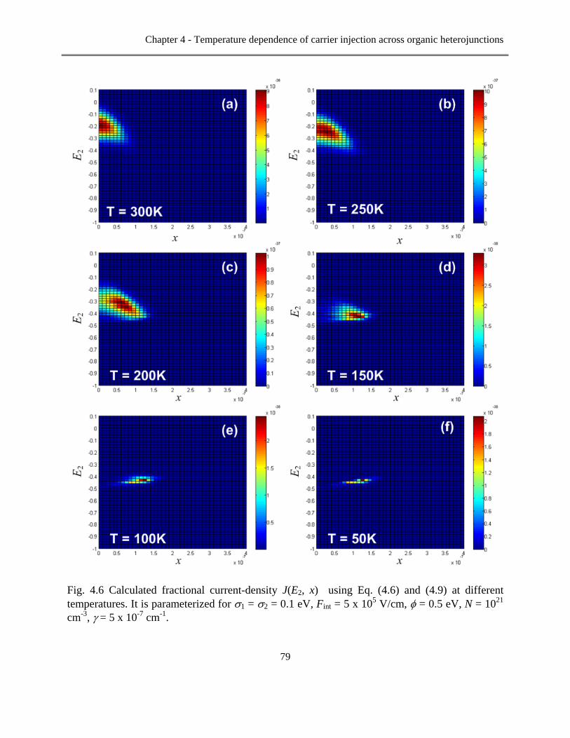
Chapter 4 - Temperature dependence of carrier injection across organic heterojunctions
79
Fig. 4.6 Calculated fractional current-density J(E2, x) using Eq. (4.6) and (4.9) at different temperatures. It is parameterized for σ1 = σ2 = 0.1 eV, Fint = 5 x 10⁵ V/cm, φ = 0.5 eV, N = 1021 cm-3, γ = 5 x 10⁻⁷ cm-1.

Chapter 4 - Temperature dependence of carrier injection across organic heterojunctions
80
Using Eq. (4.4) and ( )Exwesc , in Eq. (4.9), the temperature dependence of the injection
current with different injection barriers is shown in Fig. 4.7.
2 4 6 8 10 12 14 16 18 2010-42
10-39
10-36
10-33
10-30
10-27
10-24
10-21
10-18
10-15
10-12
lines - w/o trapssymbols - w/ traps
φ = 0.8 eV
J (a
.u.)
1000/T (K-1)
φ = 0.3 eV
Fig. 4.7 Calculated J vs 1/T characteristics using Eq. (4.4) and (4.9) as a function of barrier height φ. The lines (symbols) are calculated J without (with) deep trap states. The same parameters as in Fig. 4.5 are used in the calculation.
In the absence of traps, the temperature dependence at T > 100K increases with
increasing barrier height. This agrees with the general observation of the thermionic emission
process, and is commonly employed as the rule-of-thumb to determine the injection barrier.
Interestingly, the trend is opposite to the trend with the presence of deep trap states. The
temperature dependence decreases with increasing barrier height. It is worth nothing that, for
sufficiently large barriers, the injection current becomes temperature and barrier height

Chapter 4 - Temperature dependence of carrier injection across organic heterojunctions
81
independent, over a wide range of temperature. In that case, the injection current is mainly
contributed by the non-energetic downward hopping into the deep trap states in the second layer.
By re-plotting Fig. 4.7, the slope of J vs 1/T between 300 K and 200 K can be obtained as shown
in Fig. 4.8. It is clearly shown that, even with an extremely small density of deep trap states,
simply using the Arrhenius plot to determine the activation energy is inappropriate.
0.3 0.4 0.5 0.6 0.7 0.8
0.0
0.5
1.0
1.5
2.0
2.5
3.0 lines - w/o trapssymbols - w/ traps
- (sl
ope
of J
vs
1000
/T)
φ (eV)
Fig. 4.8 Calculated –(slope of J vs 1000/T) as a function of barrier height φ for T > 200K. The line (symbol) is calculated J without (with) deep trap states. It is parameterized for σ1 = σ2 = σt = 0.1 eV, Fint = 5 x 10⁵ V/cm, N = 1021 cm-3, γ = 5 x 10⁻⁷ cm-1, nt = 1010 cm-3, and Et = -1.5 eV.
In addition, the electric field dependence on the injection current at low temperature is
also altered by the introduction of deep trap states as shown in Fig. 8. On the one hand, without
the deep traps, the field dependence increases with decreasing temperature. Since the applied
electric field reduces the potential energy of the hopping sites in the second layer, the carriers
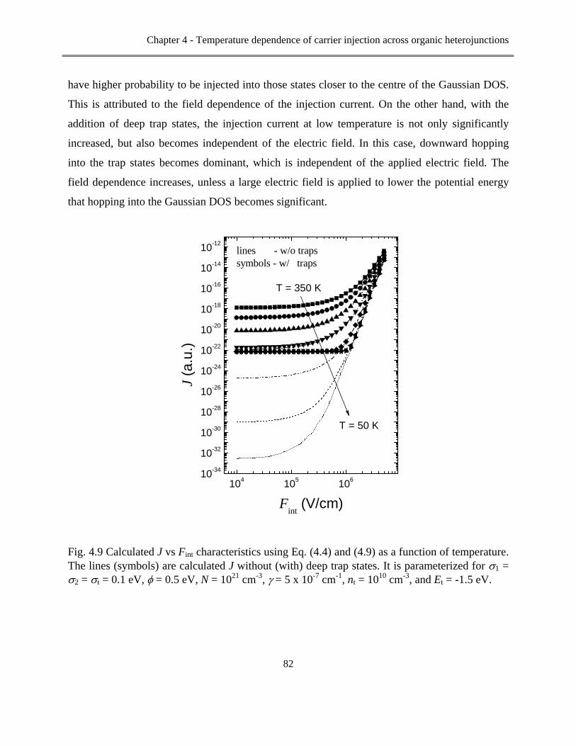
Chapter 4 - Temperature dependence of carrier injection across organic heterojunctions
82
have higher probability to be injected into those states closer to the centre of the Gaussian DOS.
This is attributed to the field dependence of the injection current. On the other hand, with the
addition of deep trap states, the injection current at low temperature is not only significantly
increased, but also becomes independent of the electric field. In this case, downward hopping
into the trap states becomes dominant, which is independent of the applied electric field. The
field dependence increases, unless a large electric field is applied to lower the potential energy
that hopping into the Gaussian DOS becomes significant.
104 105 10610-34
10-32
10-30
10-28
10-26
10-24
10-22
10-20
10-18
10-16
10-14
10-12
T = 50 K
lines - w/o trapssymbols - w/ traps
J (a
.u.)
Fint (V/cm)
T = 350 K
Fig. 4.9 Calculated J vs Fint characteristics using Eq. (4.4) and (4.9) as a function of temperature. The lines (symbols) are calculated J without (with) deep trap states. It is parameterized for σ1 = σ2 = σt = 0.1 eV, φ = 0.5 eV, N = 1021 cm-3, γ = 5 x 10⁻⁷ cm-1, nt = 1010 cm-3, and Et = -1.5 eV.

Chapter 4 - Temperature dependence of carrier injection across organic heterojunctions
83
4.4 Experiment on heterojunction devices with various injection barriers
A series of hole-only heterojunction devices with a general structure of anode / first organic layer
/ second organic layer / cathode were fabricated for this study. The hole injection barrier is
determined by the difference of the highest-occupied molecular orbital (HOMO) energy levels at
the heterojunction. The interface dipole effect on the injection barrier is ignored; as the injection
current measured at high temperature agree with trend of the HOMO energy level offset. Pre-
patterned indium tin oxide (ITO) coated on glass substrate was used as the anode. The substrate
was cleaned by a sequence of ultrasonic solvent baths and followed by UV-ozone treatment. A
320 nm layer of 4,4’,4’’-Tris(N-3-methylphenyl-N-phenyl-amino) triphenylamine (MTDATA)
was thermally evaporated on top of the ITO as the first organic layer for all of the devices. The
MTDATA layer was then covered by another thermally evaporated organic layer; 390 nm of
N,N’-diphenyl-N,N’-bis(1-naphthyl)(1,1’-biphenyl)-4,4’diamine (NPB), 430 nm of tris(8-
hydroxyquinoline) aluminum (Alq), 370 nm of 4,4’,4’’-tris(N-carbazolyl)-triphenylamine
(TCTA), or 490 nm of 2,2',2''-(1,3,5-phenylene) tris(1-phenyl-1H-benzimidazole) (TPBI).
Finally, Ag was evaporated on top of the second layer to form the cathode with an active area of
0.16 cm-2. The device structures are summarized in Table 4.1. The organic and metal layers were
fabricated in a single vacuum with a base pressure of 10-8 Torr. Thicknesses of the organic films
were measured by a stylus profilometer. The J-V characteristics of the devices were
characterized using a Keithley 236 Source-Measure unit. The carrier mobility measurement on a
single layer device with MTDATA was done by admittance spectroscopy (AS) with a HP 4284A
LRC meter. The J-V and carrier mobility measurements were performed in a temperature
regulated cryostat with a base pressure of about 10-6 Torr. During the measurement, a silicon
diode temperature sensor was attached on the glass substrate next to the test device. The
temperature was controlled and monitored by a Lakeshore 331 temperature controller. For every
20 K temperature step, 45 minutes of idle period were taken to ensure a stabilized temperature.

Chapter 4 - Temperature dependence of carrier injection across organic heterojunctions
84
first organic layer / second organic layer
HOMO energy of the 1st layer (eV)
HOMO energy of the 2nd layer (eV)
Energy offset at the heterojunction (eV)
MTDATA (320 nm) / NPB (390 nm)
5.1[4,5]
5.5 [5-8] 0.4 ± 0.1
MTDATA (320 nm) / Alq (430 nm) 5.7[8-10] 0.6 ± 0.1
MTDATA (320 nm) / TCTA (370 nm) 5.9[8] 0.8 ± 0.1
MTDATA (320 nm) / TPBI (490 nm) 6.1[11] 1.0 ± 0.1
Table 4.1 The heterojunction devices used in this study have a general structure of ITO / first organic layer / second organic layer / Ag. The energy offset at the heterojunction is determined by the energy difference of the highest-occupied molecular orbital (HOMO) of each layer.
Fig. 4.10 shows the J-Fint characteristics of the heterojunction devices at different temperatures.
For all the devices, the injection current becomes nearly temperature independent below 150 K.
In order to ensure that the pinned current is not due to the leakage current from the measurement
system, we have directly measured the current on the glass substrate. The leakage current
density, with correction for the device active layer, is around 10-11 A/cm-2. It is two orders of
magnitude lower than the measured current density of the device. It is worth noting that, for the
MTDATA/TCTA and MTDATA/TPBI devices, the hysteresis of the injection current measured
with different ramping directions of applied electric field becomes larger at lower temperature.
This suggests that there is some trap charging effects in the devices.

Chapter 4 - Temperature dependence of carrier injection across organic heterojunctions
85
0.1 110-9
10-8
10-7
10-6
10-5
10-4
0.1 1
10-9
10-8
10-7
10-6
10-5
10-4
0.1 1 10-9
10-8
10-7
10-610-9
10-8
10-7
10-6
10-5
10-4
10-3
10-2 0.1 1
(c) MTDATA/TCTA
313 K 282 K 263 K 220 K 198 K 176 K 120 K 68 K
J (A
/cm
2 )
Fint (M V/cm)
(d) MTDATA/TPBI
311 K 287 K 262 K 218 K 195 K 172 K 119 K 83 K
322 K 286 K 260 K 227 K 195 K 163 K 121 K 87 K
Fint (M V/cm)
(b) MTDATA/Alq
323 K 288 K 266 K 219 K 195 K 172 K 126 K 88 K
J (A
/cm
2 )(a) MTDATA/NPB
Fig. 4.10 Measured J vs Fint characteristics of different samples at various temperatures. (a) ITO / MTDATA (320 nm) / NPB (390 nm) / Ag, (b) ITO / MTDATA (320 nm) / Alq (430 nm) / Ag, (c) ITO / MTDATA (320 nm) / TCTA (370 nm) / Ag, and (d) ITO / MTDATA (320 nm) / TPBI (490 nm) / Ag.
Re-plotting
Fig. 4.10 at a constant Fint = 5 x 10⁵ V/cm, the temperature dependence of the injection
current for different devices is shown in Fig. 4.11. At T > 200 K, the carrier injection across the
heterojunction is still thermally activated; the injection current is higher for devices with a
smaller injection barrier. However, if one determines the activation energies from the slopes in
Fig. 4.11 at the temperature between 300 K and 200 K, as shown in the inset, it gives a
contradictory result, namely that the device with a larger injection barrier has smaller activation
energy. Moreover, at low temperature the measured currents for different devices are pinned at a

Chapter 4 - Temperature dependence of carrier injection across organic heterojunctions
86
similar value, 10-8 – 10-9A/cm-2. The measured electric field and temperature dependences are in
good agreement with the calculation results with deep trap states as shown in Fig. 4.7, Fig. 4.8,
and Fig. 4.9.
4 6 8 10 12 1410-9
10-8
10-7
10-6
10-5
10-4
10-3
10-2
0.4 0.5 0.6 0.7 0.8 0.9 1.00.6
0.8
1.0
1.2
1.4
1.6
1.8
- (sl
ope
of J
vs
1000
/T)
φ (eV)
MTDATA/TPBI
MTDATA/TCTA
MTDATA/Alq
J
(A/c
m2 )
1000/T (K-1)
Fint = 5 x 10⁵ V/cm
MTDATA/NPB
Fig. 4.11 Measured J vs 1/T characteristics of various heterojunction devices at Fint = 5 x 10⁵ V/cm. The solid lines are guides for eye vision. The inset shows the –(slope of J vs 1000/T) of different samples extracted for T > 200K.
4.5 Experiment on carrier mobility in single layer device
The calculation and experiment results discussed above suggest that the carrier injection
across the heterojunction at low temperature is dominated by an extremely small density of deep
trap states, 1010 cm-3, in the material. It is interesting to determine whether the traps originate at
the interface or in the bulk of the material. Since both the carrier transport and injection in

Chapter 4 - Temperature dependence of carrier injection across organic heterojunctions
87
disordered organic materials are hopping processes, a similar electric field and temperature
dependence of the transport properties are expected if there are any bulk trap states in the
material.
We have measured the hole mobility, μh, of MTDATA over a wide range of temperature.
Due to the weak photocurrent signal of MTDATA obtained by the time-of-flight (TOF)
technique at low temperature, AS is employed for this study.[12] In order to form a quasi-Ohmic
contact to supply enough space charges for the thin film, a thin layer of molybdenum oxide
(MoOx) has been evaporated on top of the ITO to form the injection anode.[13] The device has a
structure of ITO / MoOx (10 nm) / MTDATA (570 nm) / Ag. Fig. 4.12 shows the measured
frequency dependent capacitance at a constant applied electric field, F = 7 x 10⁵ V/cm, at
different temperatures. The position of the drop in capacitance is correlated with the carrier
transit time. At lower temperature, the minimum of capacitance shifts to lower frequency, which
indicates a larger carrier transit time and therefore a smaller carrier mobility.

Chapter 4 - Temperature dependence of carrier injection across organic heterojunctions
88
0.72
0.76
0.80
102 103 104 105
85 K
100 K
123 K
146 K
164 KF = 7 x 10⁵ V/cm
Cap
acita
nce
(nF)
(e)
(d)
(c)
(b)
Frequency (Hz)
(a)
Fig. 4.12 Measured capacitance vs frequency by admittance spectroscopy (AS) of ITO / MoOx (10 nm) / MTDATA (570 nm) / Ag devices at an applied electric field F = 7 x 10⁵ V/cm, and at temperature (a) 164 K, (b) 146 K, (c) 123 K, (d) 100 K, and (e) 85 K.

Chapter 4 - Temperature dependence of carrier injection across organic heterojunctions
89
The field and temperature dependent mobilities measured by AS are summarized in Fig.
4.13.
0 100 200 300 400 500 600 700 800 90010-9
10-8
10-7
10-6
10-5
10-4Temperature (K)
319 306 275 248 219 200 182 164 146 123 100 85
μ h (cm
2 V-1s-1
)
F1/2 [(V/cm)1/2]
Fig. 4.13 The average hole mobility μh of MTDATA measured by admittance spectroscopy (AS) at various temperatures. The solid lines are the best fits to the Poole-Frenkel expression:
( )Fh βμμ exp0= , where μ0 is a prefactor, β is the electric field dependence coefficient, and F is the applied electric field.
By re-plotting Fig. 4.13, the temperature dependence of the mobility at F = 5 x 10⁵ V/cm
is shown in Fig. 4.14. The temperature dependence is similar to those observed in the
heterojunction devices; the mobility is pinned at a constant value at low temperature. It has been
proposed that the carrier mobility can be formulated with the consideration of carrier
concentration p as:[14]

Chapter 4 - Temperature dependence of carrier injection across organic heterojunctions
90
( ) ( )( )[ ]∫∫ ∞−
−
∞−⎟⎠⎞
⎜⎝⎛ −
−+⎥⎦⎤
⎢⎣⎡= trtr E tr
F
E
h kTEE
kTEEEgdEEgdE
kTpe exp
/exp1
3/20ν
μ
(4.11)
where Etr is the effective transport level of energy, EF is the Fermi level. In a space-charge
limited (SCL) regime, the average value of p is equal to ( )20 /2/3 edVrεε ,[15] where ε0 is the
permittivity of free space, εr is the relative dielectric constant, and d is the thickness of the
organic film. For F = 5 x 10⁵ V/cm, d = 570 nm and εr = 3, we get p = 2.15 x 1016 cm-3. The
solid line in Fig. 4.14 is calculated using Eq. (4.11) with 0ν = 3 x 10¹³ s-1, γ = 3 x 107 cm-1, N =
1021 cm-3 and σ = 0.1 eV. Those parameters are comparable to values previously reported.[2] At T
> 180 K, there is good agreement between the calculation and experimental results. However, the
measured mobility is a few orders of magnitude higher below 100 K.
0 30 60 90 120 15010-15
10-13
10-11
10-9
10-7
10-5
10-3
F = 5 x 10⁵ V/cm
measured extrapolated from Fig. 16 calculated with Eq. (10)
μ h (cm
2 V-1s-1
)
(1000/T)2 (K-2)
Fig. 4.14 Measured μh vs 1/T2 characteristics of MTDATA at F = 5 x 10⁵ V/cm. The solid symbols are directly measured data. The open symbols are extrapolated from Fig. 4.13. The solid line is the best fit to data using Eq. (4.11), with σ = 0.1 eV, N = 1021 cm-3, ν = 3 x 10¹³ s-1, γ = 5 x 10⁻⁷ cm-1, and p = 2.15 x 1016 cm-3.
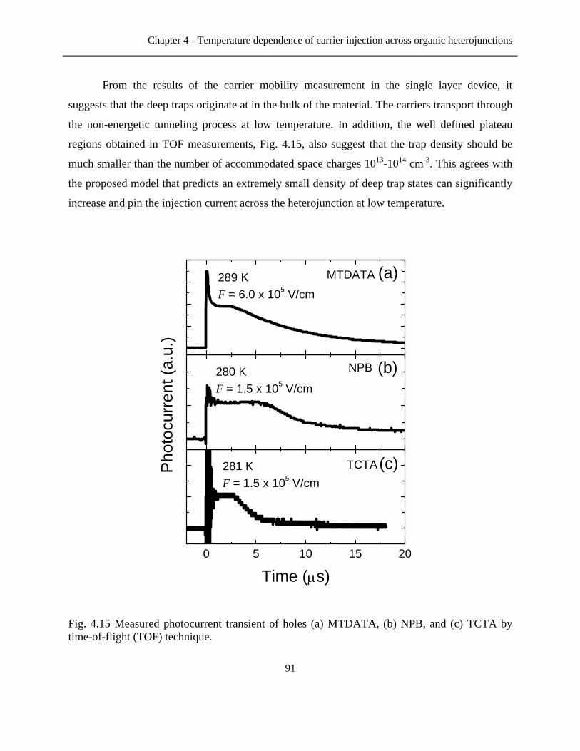
Chapter 4 - Temperature dependence of carrier injection across organic heterojunctions
91
From the results of the carrier mobility measurement in the single layer device, it
suggests that the deep traps originate at in the bulk of the material. The carriers transport through
the non-energetic tunneling process at low temperature. In addition, the well defined plateau
regions obtained in TOF measurements, Fig. 4.15, also suggest that the trap density should be
much smaller than the number of accommodated space charges 1013-1014 cm-3. This agrees with
the proposed model that predicts an extremely small density of deep trap states can significantly
increase and pin the injection current across the heterojunction at low temperature.
0 5 10 15 20
281 KF = 1.5 x 10⁵ V/cm
Pho
tocu
rren
t (a.
u.)
Time (μs)
TCTA
280 KF = 1.5 x 10⁵ V/cm
(c)
(b)NPB
MTDATA (a)289 KF = 6.0 x 10⁵ V/cm
Fig. 4.15 Measured photocurrent transient of holes (a) MTDATA, (b) NPB, and (c) TCTA by time-of-flight (TOF) technique.

Chapter 4 - Temperature dependence of carrier injection across organic heterojunctions
92
4.6 Discussion
We have considered adding trap states, Eq. (4.10), into the analytical mobility model in
Eq. (4.11). However, in order to reduce the temperature dependence, one has to choose a density
of trap states close to that of the space charge 1016 cm-3. This can be understood by the fact that
Eq. (4.11) is based on carrier transport at the transport energy level Etr. It will be changed only if
the number of additional trap states is large enough to redistribute the carriers in the DOS.
Nevertheless, the calculated mobility with 1016 cm-3 trap states still has a higher temperature
dependence then the experimental results. Such a trap density is also much higher than the
number of photo-excited carriers in TOF measurements. Moreover, an unrealistic value of
phonon frequency 0ν = 1016 s-1 has to be used in Eq. (4.11) to fit the data. We have measured the
temperature dependence of injection current for various single layer devices with different
injection barriers at the metal/organic interfaces.[16] It is found that the temperature dependence
has also decreased with a larger injection barrier. Similar temperature dependence has also been
reported by Baldo et al. on electron injection from metals into Alq.[17] Therefore, it is believed
that carrier transport and injection pinned at low temperature by the presence of an extremely
small density of deep trap states is a general feature in disordered organic materials. As such
small number of trap states exists even in high-purity inorganic crystal, such as silicon.
4.7 Conclusion
An injection model with a proposed escape probability function wesc based on the total
hopping frequencies at both sides of the organic heterojunction is formulated. It has been shown
that the injection current at low temperature is greatly increased and pinned by an extremely
small density of deep trap states 1010 cm-3. As a result, the injection current across a
heterojunction with a larger injection barrier has a smaller temperature dependence. The
calculation results are in good agreement with the experimental results of heterojunction devices

Chapter 4 - Temperature dependence of carrier injection across organic heterojunctions
93
with barrier heights ranging from 0.4 eV – 1.0 eV. We have also demonstrated that the carrier
mobility in a single layer device shows similar temperature dependence. This strongly supports
that the small number of deep trap states originate from the bulk of the material instead of only
from the interface. This study also suggests that, in the presence of the deep trap states, simply
extracting the barrier height from the Arrhenius plot is inappropriate.

Chapter 4 - Temperature dependence of carrier injection across organic heterojunctions
94
4.8 References
[1] A. Miller and E. Abrahams, Phys. Rev. 120, 745 (1960).
[2] S. W. Tsang, M. W. Denhoff, Y. Tao, and Z. H. Lu, Phys. Rev. B 78, 081301 (2008).
[3] V. I. Arkhipov, E. V. Emelianova, and H. Bassler, J. Appl. Phys. 90, 2352 (2001).
[4] C. Giebeler, H. Antoniadis, D. D. C. Bradley, and Y. Shirota, Appl. Phys. Lett. 72, 2448
(1998).
[5] C. Adachi, R. Kwong, and S. R. Forrest, Org. Electron. 2, 37 (2001).
[6] A. Wan, J. Hwang, F. Amy, and A. Kahn, Org. Electron. 6, 47 (2005).
[7] T. Chasse, C. I. Wu, I. G. Hill, and A. Kahn, J. Appl. Phys. 85, 6589 (1999).
[8] M. Ikai, S. Tokito, Y. Sakamoto, T. Suzuki, and Y. Taga, Appl. Phys. Lett. 79, 156
(2001).
[9] A. Rajagopal and A. Kahn, Adv. Mater. 10, 140 (1999).
[10] Y. Q. Li, J. X. Tang, and L. S. Hung, Chem. Phys. Lett. 376, 90 (2003).
[11] Z. Gao, C. S. Lee, I. Bello, S. T. Lee, R.-M. Chen, T.-Y. Luh, J. Shi, and C. W. Tang,
Appl. Phys. Lett. 74, 865 (1999).
[12] S. W. Tsang, S. K. So, and J. B. Xu, J. Appl. Phys. 99, 013706 (2006).
[13] M. Hoping, C. Schildknecht, H. Gargouri, T. Riedl, M. Tilgner, H. H. Johannes, and W.
Kowalsky, Appl. Phys. Lett. 92, 213306 (2008).
[14] V. I. Arkhipov, P. Heremans, E. V. Emelianova, G. J. Adriaenssens, and H. Bassler,
Appl. Phys. Lett. 82, 3245 (2003).
[15] M. A. Lampert and P. Mark, Current Injection into Solids. (Academic, New York, 1970).
[16] Z. B. Wang, M. G. Helander, S. W. Tsang, and Z. H. Lu, Phys. Rev. B sumitted (2008).
[17] M. A. Baldo and S. R. Forrest, Phys. Rev. B 64, 085201 (2001).
95
Chapter 5 Engineering carrier transport across organic heterojunctions
by interface doping
5.1 Abstract
In this Chapter, it will be shown that injection current at an organic heterojunction can be
effectively engineered by introducing a thin (2 nm) p-doped interlayer at the junction. Two
common hole transporting materials, 4,4’,4’’-Tris(N-3-methylphenyl-N-phenyl-amino)
triphenylamine (MTDATA) and N,N’-diphenyl-N,N’-bis(1-naphthyl)(1,1’-biphenyl)-
4,4’diamine (NPB), and p-type dopant tetra-fluorotetracyanoquinodimethane (F4-TCNQ), were
used to build various test devices. For a hole-only heterojunction device, ITO / MTDATA / NPB
/ Ag, both experimental measurement and theoretical modeling showed that the current flow in
the device is limited by the heterojunction potential barrier or band-offset at the MTDATA/NPB
interface. It is found that the device current flow can be modulated dramatically to increase or
decrease by introducing a 2 nm p-doped NPB:F4-TCNQ or MTDATA:F4-TCNQ interlayer,
respectively. Quasi-Fermi energy level realignment at the doped/undoped organic-organic
interface is proposed as the working principle for the observed phenomena.

Chapter 5 - Engineering carrier transport across organic heterojunctions by interface doping
96
5.2 Introduction
Organic light-emitting diode (OLED) is a key technology for flat-panel displays and has
huge potential for future lighting applications. The current high research activities in OLED was
triggered by the first seminal report of constructing the device using organic-organic
heterojunction,[1] which is now the standard device platform in commercial production.
Heterojunctions provide a practical engineering method to modulate carrier (electrons or holes)
concentration in the device thus leading to much improved stability and efficiency. For
multilayered structures with no intrinsic free carriers inside the device, charge carriers
(electrons/holes) have to be injected from two opposite electrodes (cathode/anode). These
injected carriers have to pass through different organic layers before they form excitons in the
emission layer. In the past decade, there were numerous studies on the metal/organic (MO)
interface. It has been successfully demonstrated that the injection can be improved by
modification at the MO interface. In some case, true Ohmic contact at MO interface has been
demonstrated.[2] As a result, operating voltage in OLEDs has been improved steadily over the
last decade. One of the current challenges in OLED device physics is to understand and control
of charge transport across organic-organic interface (OOI). It is well-known that energy offset
exists at any heterojunctions. In conventional inorganic semiconductor devices, e.g. laser diode,
heterojunction plays a critical role in device performance. In organic electronic materials, such
energy offset has been shown to be the major factor limiting the injection current at the organic-
organic interface OOI.[3-5] This is therefore important to understand and to control the carrier
transport across the OOI. The current approach to this problem is mostly chemistry-type, i.e.
synthesizing and matching various classes of organic derivatives. Due to many restrictions such
as optical path, molecular stability, carrier mobility etc., the choice of practical materials and
even thickness for each layer are quite often limited. In this letter, we report an alternative
physical method which involves inserting a thin p-doped interlayer at the OOI to effectively
modulate the carrier transport across the heterojunction. Controlling the injection current with
the doped-interlayer at OOI can be applied to balance the electron and hole currents in the
device. Balancing electron and hole currents has been proved to be a determining factor for the
device efficiency in OLED. The doping mechanism is illustrated in Fig. 5.1. F4-TCNQ is a
strong electron acceptor which has the LUMO energy level closes to the HOMO energy level of

Chapter 5 - Engineering carrier transport across organic heterojunctions by interface doping
97
NPB. The occupied electron states in NPB can be readily transferred to the F4-TCNQ that
increases the hole concentration in NPB molecules and forms a p-doped layer. Furthermore,
theoretical modeling was used to explain the current-voltage characteristics using these
materials’ physical parameters independently extracted by time-of-flight (TOF) technique using
method reported in Ref. [6].
Charge transfer
matrix dopant matrix dopant
N
N
NN
Me
Me
MeC
CN
CNC
NC
NC
FF
FF N
N
NN
Me
Me
MeC
CN
CNC
NC
NC
FF
FF
LUMO
HOMO
LUMO
HOMO
LUMO
HOMO
LUMO
HOMO
MTDATA F4TCNQ MTDATA F4TCNQ
Fig. 5.1 Schematic diagram of p-type doping of an organic matrix (MTDATA) with a p-type dopant (F4-TCNQ).
5.3 Experiment
Simple double layer hole-only devices were used for this study. The devices have a
general structure: substrate/anode/organic layer-I /organic layer-II /cathode. Pre-patterned
indium tin oxide (ITO) on glass was used as the anode. The ITO substrate was cleaned by
acetone then methanol in ultra-sonic baths followed by uv-ozone treatment. Two hole
transporting materials 4,4’,4’’-Tris(N-3-methylphenyl-N-phenyl-amino) triphenylamine

Chapter 5 - Engineering carrier transport across organic heterojunctions by interface doping
98
(MTDATA, from Syntec GmbH) and N,N’-diphenyl-N,N’-bis(1-naphthyl)(1,1’-biphenyl)-
4,4’diamine (NPB, from H. W. Sands) were used to form the various types of organic
heterojunctions. The highest-occupied molecular orbital (HOMO) of MTDATA and NPB are 5.1
eV and 5.4 eV, respectively.[7,8] Therefore there exists a hole injection barrier of 0.3 eV from
MTDATA to NPB. The organic films were thermally evaporated on top of the ITO substrate in
vacuum with a base pressure of 10-7 Torr. It was then followed by evaporating silver (Ag) as the
top contacting cathode. Due to a large energy difference between the work function of Ag (4.3
eV) and the lowest unoccupied molecular orbital (LUMO) (< 2.5 eV) of the organic materials,
Ag cathode is restricted from injecting electrons into in these devices. In some devices, a p-
doped interlayer was inserted at the OOI. The p-doped interlayer was achieved by co-evaporation
of host (MTDATA or NPB) and p-type dopant, tetra-fluorotetracyanoquinodimethane (F4-
TCNQ, 99.9% purity, from Lumtec. Co. Ltd). The doping ratio (in molar %) was controlled by
independently monitoring the evaporation rates of the host and the dopant. The device structures
used for this study are summarized in Table 5.1.
Device Organic layer I Interlayer Organic layer II
A MTDATA (236 nm) / ----- / NPB (82 nm)
B MTDATA (236 nm) / NPB:F4-TCNQ (2 nm, 10%) / NPB (80 nm)
C MTDATA (234 nm) / MTDATA:F4-TCNQ (2 nm, 10%) / NPB (82 nm)
D MTDATA (234 nm) / MTDATA:F4-TCNQ (2 nm, 15%) / NPB (82 nm)
E MTDATA (236 nm) / ----- / -----
Table 5.1 Structures of various test devices used in this work. All double layer devices have the same total thickness of organic films (318 nm). For device B, C and D, there is a thin (2 nm) p-doped (10 % or 15 % molar ratio) interlayer.
For time-of-flight (TOF) measurements, thick film (3-4 μm) of MTDATA or NPB was
thermally evaporated onto ITO coated glass substrate. Semitransparent aluminum (Al) electrode
was used as the positively bias electrode. The organic film was photoexcited by a frequency-
tripled Nd:YAG pulsed laser (λ = 355 nm, pulsed width = 6 ns). A dc power supply (Stanford
PS310) was used to provide an external voltage to extract photogenerated holes. The
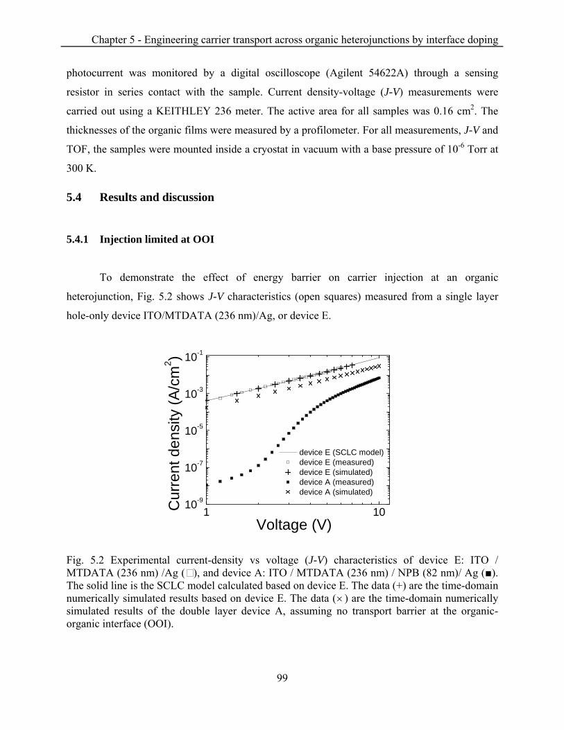
Chapter 5 - Engineering carrier transport across organic heterojunctions by interface doping
99
photocurrent was monitored by a digital oscilloscope (Agilent 54622A) through a sensing
resistor in series contact with the sample. Current density-voltage (J-V) measurements were
carried out using a KEITHLEY 236 meter. The active area for all samples was 0.16 cm2. The
thicknesses of the organic films were measured by a profilometer. For all measurements, J-V and
TOF, the samples were mounted inside a cryostat in vacuum with a base pressure of 10-6 Torr at
300 K.
5.4 Results and discussion
5.4.1 Injection limited at OOI To demonstrate the effect of energy barrier on carrier injection at an organic
heterojunction, Fig. 5.2 shows J-V characteristics (open squares) measured from a single layer
hole-only device ITO/MTDATA (236 nm)/Ag, or device E.
1 1010-9
10-7
10-5
10-3
10-1
device E (SCLC model) device E (measured) device E (simulated) device A (measured) device A (simulated)
Cur
rent
den
sity
(A/c
m2 )
Voltage (V)
Fig. 5.2 Experimental current-density vs voltage (J-V) characteristics of device E: ITO / MTDATA (236 nm) /Ag ( ), and device A: ITO / MTDATA (236 nm) / NPB (82 nm)/ Ag (). The solid line is the SCLC model calculated based on device E. The data (+) are the time-domain numerically simulated results based on device E. The data (× ) are the time-domain numerically simulated results of the double layer device A, assuming no transport barrier at the organic-organic interface (OOI).

Chapter 5 - Engineering carrier transport across organic heterojunctions by interface doping
100
The solid line is a theoretical J-V curve calculated based on the trap-free space-charge-
limited current (SCLC) model with field dependent mobility[9]
( ) 3
2
00 89.0exp89
LVEJ rSCLC βμεε= (5.1)
where εr = 3 is the relatively permittivity and is obtained by measuring the device capacitance, ε0
is the absolute permittivity, E is the applied electric field, V is the applied voltage bias and L is
the organic film thickness. The zero field hole mobility μ0 = 1.28 x 10⁻⁵ cm2V-1s-1 and field
dependent coefficient β = 1.88 x 10⁻³ (V/cm)-1/2 were obtained independently by TOF technique.
The excellent agreement between the measured and calculated current densities proves that the
conduction is dominated by the bulk organic film and contact resistance between ITO and
MTDATA is negligible.[7,10] The results have been further verified with differential time-domain
numerical simulation using a method reported by Ref. [11]. Thus zero contact resistance was
used as the boundary condition. The simulated steady current densities were obtained at different
bias voltages (symbols (+)). The measured, calculated and simulated results are all in excellent
agreement with each other.
The measured J-V characteristics of a double layer device ITO / MTDATA (236 nm) /
NPB (82 nm) / Ag (filled square), device A, is also shown in Fig. 5.2. By using TOF technique,
μ0 and β of NPB were found to be 5.27 x 10⁻⁴ cm2V-1s-1 and 1.80 x 10⁻³ (V/cm)-1/2, respectively.
Although the hole mobility of NPB is more than one order of magnitude higher than that of
MTDATA, the measured J of the double layer device is much lower than that of the single layer
device. This is attributed to a hole transport barrier (0.3 eV) at the MTDATA / NPB interface. In
order to illustrate the effect of transport barrier at the OOI, the maximum attainable current in the
double layer device was simulated (shown in cross × in Fig. 5.2) using time-domain simulation
method (Ref. [11]) by assuming no barrier at the OOI. Briefly in the simulation, the holes were
injected at the anode with no resistance, and then drifted along the applied electric field moving
through MTDATA then through NPB. In this case, the current is only limited by the space
charges inside the organic layers. By comparing the simulation results with the measured J,

Chapter 5 - Engineering carrier transport across organic heterojunctions by interface doping
101
especially at low field region, it is clear that the current in the double layer device is significantly
limited by the presence of a potential barrier at the OOI.
5.4.2 Engineering carrier injection by interface doping at OOI
Fig. 5.3 shows J-V characteristics of double layer devices with inclusion of various types
of p-doped interlayers. In device B, a thin layer of NPB:F4-TCNQ (2 nm) is placed between
MTDATA and NPB. It is found that the measured J (filled circles) is significantly increased
upon the insertion of the NPB:F4-TCNQ interlayer. However, when the interlayer is replaced by
MTDATA:F4-TCNQ (2 nm) as in device C, the measured J (filled upward triangles) is
dramatically reduced. In device D, the measured J (filled downward triangles) is found to be
further suppressed by increasing the doping ratio to 15%.
10
10-7
10-5
10-3
device A (simulated) device A (measured) device B (measured) device C (measured) device D (measured)
Cur
rent
den
sity
(A/c
m2 )
Voltage (V)
Fig. 5.3 Current-density voltage (J-V) characteristics of various double layer devices: device A () without an interlayer; device B ( ) with an interlayer NPB:F4-TCNQ (2 nm, 10%); device C ( ) with an interlayer MTDATA:F4-TCNQ (2 nm, 10%); device D ( ) with an interlayer MTDATA:F4-TCNQ (2 nm, 15%). The data (× ) are the time-domain numerically simulated results based on device A, assuming no transport barrier at the organic-organic interface (OOI).

Chapter 5 - Engineering carrier transport across organic heterojunctions by interface doping
102
5.4.3 Energy alignment at OOI with doped inter-layer
It is well known that doping can effectively increase the charge-carrier concentration in
organic semiconductors.[12,13] Furthermore, it has also been demonstrated that doping can induce
energy level realignment at the OOI.[14,15] Devices B, C and D all contain a heavily p-doped
interlayer at the junction. Despite the fact that the hole concentration in the p-doped interlayer is
much higher than those in the undoped matrix, the measured current densities of devices C and D
are much lower than the undoped device A. Therefore, it is reasonable to assume that the
effective injection barrier is increased by the energy level realignment at the OOI due to doping.
The schematic energy diagrams of the double layer devices are depicted in Fig 5.4. In device A,
the hole injection barrier is attributed to the HOMO energy levels difference (0.3 eV) between
MTDATA and NPB, and the device hole current mainly determined by the efficiency of hole
injection across MTDATA/NPB heterojunction. In the following discussion, effective p-type
doping of NPB and MTDATA has been assumed. The p-type doping induced change in the
Fermi level and carrier concentration have been reported.[12,13,16] In device B, the p-type-doping
reduces the energy gap between Fermi level and HOMO of NPB inside the interlayer. As a
results, the HOMO offset at the NPB/NPB:F4-TCNQ interlayer is effectively reduced and
consequently transport barrier at the MTDATA/NPB is now reduced. In this case, the interlayer
functions as an intermediate energy level that facilitates hole injection into NPB. In device C or
D, similarly, the energy gap between Fermi level and HOMO of the MTDATA:F4-TCNQ
interlayer is reduced by p-doping. In this case, however, this uplifting in the HOMO energy level
leads to an increase in the hole injection barrier. The injected holes from the MTDATA will be
initially trapped inside the interlayer, and then these carriers will have to overcome a larger
energy barrier in order to be injected from the interlayer into NPB. As a result, the current
density in device C and D is much reduced when compared with undoped device A.
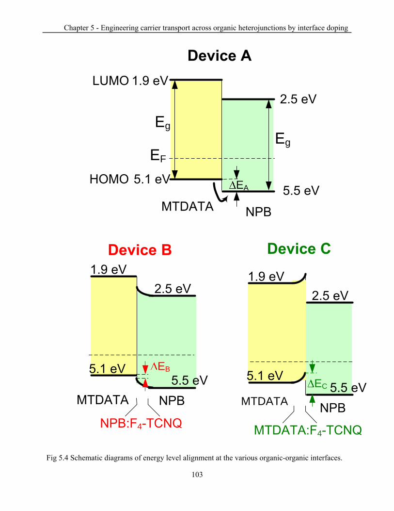
Chapter 5 - Engineering carrier transport across organic heterojunctions by interface doping
103
F
g
g
44
MTDATA
EA
EB
EC
Fig 5.4 Schematic diagrams of energy level alignment at the various organic-organic interfaces.

Chapter 5 - Engineering carrier transport across organic heterojunctions by interface doping
104
5.5 Conclusion
In conclusion, we have shown, in both experiment and theoretical simulation, that charge
transport in double layer device is limited by a potential barrier at the organic-organic
heterojunction. We have demonstrated that this transport barrier at the organic heterojunction can
be effectively modulated by introducing a thin (2 nm) p-doped interlayer at the heterojunction. It
is found that charge transport across MTDATA/NPB heterojunction can be easily modulated by
inclusion of a doped interlayer at the junction; NPB:F4-TCNQ interlayer for increasing hole
current or MTDATA:F4-TCNQ interlayer for decreasing hole current. A change in the quasi
Fermi level upon doping together with energy level alignment at the heterojunctions were
proposed as the underling physics principle to explain the observed phenomena. The junction
doping technique provides an promising alternative process pathway to module electron or hole current in
organic electronic devices using commonly available organic semiconductor molecules.

Chapter 5 - Engineering carrier transport across organic heterojunctions by interface doping
105
5.6 References
[1] C. W. Tang and S. A. VanSlyke, Appl. Phys. Lett. 51, 913 (1987).
[2] X. D. Feng, C. J. Huang, V. Lui, R. S. Khangura, and Z. H. Lu, Appl. Phys. Lett. 86,
143511 (2005).
[3] V. I. Arkhipov, E. V. Emelianova, and H. Bassler, J. Appl. Phys. 90, 2352 (2001).
[4] T. v. Woudenbergh, J. Wildeman, and P. W. M. Blom, Phys. Rev. B 71, 205216 (2005).
[5] S. W. Tsang, M. W. Denhoff, Y. Tao, and Z. H. Lu, Phys. Rev. B 78, 081301 (2008).
[6] P. M. Borsenberger and D. S. Weiss, Organic Photoreceptors for Imaging Systems
(Dekker, New York, 1993).
[7] C. Giebeler, H. Antoniadis, D. D. C. Bradley, and Y. Shirota, Appl. Phys. Lett. 72, 2448
(1998).
[8] A. Wan, J. Hwang, F. Amy, and A. Kahn, Org. Electron. 6, 47 (2005).
[9] P. N. Murgatroyd, J. Phys. D 3, 151 (1970).
[10] S. W. Tsang, K. L. Tong, S. C. Tse, and S. K. So, presented at the Proc. SPIE, 2006
(unpublished).
[11] G. G. Malliaras and J. C. Scott, J. Appl. Phys. 83, 5399 (1998).
[12] X. Zhou, M. Pfeiffer, J. Blochwitz, A. Werner, A. Nollau, T. Fritz, and K. Leo, Appl.
Phys. Lett. 78, 410 (2001).
[13] M. Pfeiffer, K. Leo, X. Zhou, J. S. Huang, M. Hofmann, A. Werner, and J. Blochwitz-
Nimoth, Org. Electron. 4, 89 (2003).
[14] A. Kahn, W. Zhao, W. Gao, H. Vázquez, and F. Flores, Chem. Phys. 325, 129 (2006).
[15] S. D. Wang, K. Kanai, E. Kawabe, Y. Ouchi, and K. Seki, Chem. Phys. Lett. 423, 170
(2006).
[16] W. Gao and A. Kahn, J. Appl. Phys. 94, 359 (2003).

106
Chapter 6 Impact of energy offset at organic heterojunctions on organic
lightemitting diodes (OLEDs)
6.1 Abstract
The impact of energy offset at organic heterojunctions on organic light-emitting diodes(OLEDs)
is investigated by interface doping. This technique provides a means to modulate the charge
carrier transport across an organic heterojunction without interfering with the bulk transport
properties. It is shown that a thin (2 nm) p-type doped interlayer at the hole injection layer (HTL)
/ hole transporting layer (HTL) interface can effectively increase the device current. As a
consequence, the power efficiency of a device is increased by up to 24 %. It is found that unlike
charge carrier injection at metal-organic (MO) interfaces, an energy barrier height of 0.3 eV will
still limit the charge carrier transport across organic-organic interfaces (OOIs). This is explained
by the charge carrier distribution in a Gaussian density-of-state (DOS) in disordered electronic
materials. The charge carriers mean energy in donor molecules are localized away from the
centre of Gaussian DOS and this makes charge carrier injection less efficient at OOI.

Chapter 6 - Impact of energy offset at organic heterojunctions on organic light-emitting diodes (OLEDs)
107
6.2 Introduction to multilayer OLEDs
Since the discovery of the first highly efficient organic heterojunction light-emitting
diode (OLED) by Tang et al in the 1980s,[1] extensive research has been conducted on organic
semiconductors and devices. Although the OLED is now a contender in flat-panel display
market, higher device efficiency is desired, especially for lighting applications. The general
structure of an OLED consists of multi-layers of organic thin films sandwiched by two
electrodes, which include the anode / hole injection layer (HIL) / hole transporting layer (HTL) /
electro-luminance layer (EL) / electron transporting layer or hole blocking layer (ETL or HBL) /
cathode. In the past few decades, extensive research has been reported on the electronic
properties of metal-organic (MO) interfaces. In order to have higher injection efficiency, the
transporting site energy of organic materials must match the work function of electrodes. It has
been shown that modifying the MO interfaces has a large impact on both device efficiency and
stability.[2,3] Furthermore it has also been analytically and experimentally demonstrated that
quasi-Ohmic contacts can be achieved when the energy barrier at MO interfaces is less than 0.3
eV.[4]
Compared to a MO interface, the issue of charge carrier transport at organic-organic
interfaces (OOIs) has been overlooked. Arkhipov et al. has proposed an analytical model to
describe charge carrier hopping at the interface separating two disorderd organic materials.[5] It
was shown that the majority of interfacial jumps are roundtrip ones and only very few jumps lead
to true charge injection. As a result, carrier recombination at OOI is much higher than that
predicted by conventional Langevin theory.[6,7] The OOI model is further justified by
Woudenbergh et al with experimental results of a polymeric heterojunction, poly-phenylene
vinylene derivative (PPV) / poly(9,9-dioctylfluorene) (PFO).[8] It has been demonstrated that the
polymeric heterojunction strongly limits the hole current due to an interface energy barrier. The
current densities at a high electric field (>106 V/cm) are in agreement with the OOI model.
However, the strong field dependence of the current densities in the lower field region must take
into account the effect of charge carrier distribution in a Gaussian density-of-state (DOS) of
PPV. Details of carrier injection at OOI have been discussed in Chapters 3 and 4.

Chapter 6 - Impact of energy offset at organic heterojunctions on organic light-emitting diodes (OLEDs)
108
In the present study, the impact of energy offset at organic heterojunctions on OLEDs is
investigated by interface doping. The interface doping technique provides a means to modulate
charge carrier transport at the OOI without changing its bulk properties.[9] It will be shown that
energy offsets at OOIs play an important role by limiting the current and lowering the power
efficiency of OLEDs. Unlike the case of MO interface, where a quasi-Ohmic contact is formed
when the energy barrier is less than 0.3 eV, it is found that such an energy barrier can still
suppress carrier injection at an OOI. This issue will be discussed with the concept of carrier
distribution in ordered organic materials.
6.3 Experiment
The OLEDs used for this study have a general structure of glass substrate / indium tin
oxide (ITO) / hole injection layer (HIL) / hole transporting layer (HTL) / electro-luminance layer
(EL) / hole blocking layer (HBL) / Lithium fluoride (LiF) / Aluminium (Al). 4,4’,4’’-Tris(N-3-
methylphenyl-N-phenyl-amino) triphenylamine (MTDATA) was used as the HIL. N,N’-
diphenyl-N,N’-bis(1-naphthyl)(1,1’-biphenyl)-4,4’diamine (NPB) was used as the HTL. In order
to investigate the impact of energy level offset at the organic heterjunctions on device
performance, three different electro-luminance materials were chosen to fabricate the ELs. Their
highest occupied molecular orbital (HOMO) energy levels vary from 5.4 eV to 5.8 eV.
Aluminum tris(8-hydroxyquinoline) (Alq3) with a HOMO energy level equal to 5.7 eV was used
in device A.[10] Mes2B(p-4,4´-biphenyl-NPh(1-naphthyl)) (BNPB) with a HOMO energy level
equal to 5.4 eV was used in device B.[11] 2,6-di(t-butyl)-9,10-di-(2-naphthyl)anthracene
(TBADN) with a HOMO energy level equal to 5.8 eV was used in device C.[12] In device B and
C, there was a HBL 2,2',2''-(1,3,5-phenylene) tris(1-phenyl-1H-benzimidazole) (TPBI). The pre-
patterned ITO anode was cleaned by a series of ultrasonic baths with deionized water, methanol
and acetone, and followed by uv-ozone treatment. The organic layers were sequentially
deposited on top of the ITO in a vacuum chamber with a base pressure of 10-8 Torr. It was then
followed by depositing of LiF (1 nm) and Al (100nm) to form the cathode contact. In some of
the devices, a thin p-doped interlayer (2 nm) was inserted at the MTDATA/NPB interface. The
p-doped interlayer was achieved by coevaporation of NPB and a p-type dopant, tetra-

Chapter 6 - Impact of energy offset at organic heterojunctions on organic light-emitting diodes (OLEDs)
109
fluorotetracyanoquinodimethane (F4-TCNQ). Details of the device structures are summarized in
Table 6.1.
The devices were encapsulated before being removed from the vacuum chamber. The
device characteristics were measured by a HP 4140B picoammeter and a Minolta LS-110
luminance meter.
Devices HIL (nm)
Interlayer (molar %, nm)
HTL (nm)
EL (nm)
HBL (nm)
A1 MTDATA
(40)
------ NPB (45)
Alq3 (50) ------ A2 NPB:F4TCNQ (6%, 2)
A3 NPB:F4TCNQ (18%, 2) A4 NPB:F4TCNQ (50%, 2) B1
MTDATA (25)
------ NPB (45)
BNPB (20)
TPBi (30)
B2 NPB:F4TCNQ (7%, 2) B3 NPB:F4TCNQ (21%, 2) B4 NPB:F4TCNQ (50%, 2) C1
MTDATA (25)
------ NPB (45)
TBADN (20)
TPBi (30)
C2 NPB:F4TCNQ (10%, 2) C3 NPB:F4TCNQ (17%, 2) C4 NPB:F4TCNQ (67%, 2)
Table 6.1 Structures of various test devices used in this study. In general, the devices consist of ITO / HIL / HTL / EL / HBL / LiF / Al. In some of the devices, there is a 2 nm p-type doped interlayer NPB:F4TCNQ at the HIL / HTL interface.
6.4 Results and discussion
As shown in Fig. 6.1 the energy diagrams of the devices, the injected holes from the
anode to the EL encounter energy barriers at the MTDATA/NPB and NPB/EL interfaces.
Interface doping with different doping concentrations has been employed to modify the hole
transport across the MTDATA/NPB interface. [9]

Chapter 6 - Impact of energy offset at organic heterojunctions on organic light-emitting diodes (OLEDs)
110
Fig. 6.1 Energy diagrams of device A, B and C with HOMO energy levels (eV) for different organic materials.
6.4.1 Organic-organic hole injection barrier in Alq3 devices
In device A, there is a 0.3 eV energy barrier for hole transport across both the
MTDATA/NPB and NPB/Alq3 interfaces. As shown in Fig. 6.2(a), for devices A2, A3, and A4,
the current densities are increased with a 2 nm NPB:F4TCNQ interlayer at the MTDATA/NPB
interface. At low and high electric field regions, the current densities can be increased by 3 and
half orders of magnitude, respectively. This is consistent with the double layer device as reported
earlier.[9] As depicted in Fig. 6.2(b), the luminance of the device is also increased by a half order
of magnitude. As a result, the operating voltage is reduced by 2 V.

Chapter 6 - Impact of energy offset at organic heterojunctions on organic light-emitting diodes (OLEDs)
111
0 2 4 6 8 10 12
10-6
10-4
10-2
100
102
0 2 4 6 8 1012
10-1
100
101
102
103
104
(b)(a)
Cur
rent
den
sity
(mA
/cm
2 )
Voltage (V)
Lum
inan
ce (c
d/m
2 )
Voltage(V)
Devices A1 A2 A3 A4
Fig. 6.2 (a) Current-density vs voltage (J-V) and (b) luminance vs voltage (L-V) characteristics of a series of device A. Device A1 without an interlayer; Device A2 with an interlayer NPB:F4TCNQ (molar ratio 6%, 2 nm); Device A3 with an interlayer NPB:F4TCNQ (molar ratio 18%, 2 nm); Device A4 with interlayer an NPB:F4TCNQ (molar ratio 50%, 2 nm).
However, in Fig. 6.3, there is no change in the current efficiencies for all devices both with and
without the interlayer. This can be attributed to the equal improvements of the current density
and luminance as discussed before. It also indicates that the electron and hole densities in EL
have equal improvement; otherwise the current efficiency will drop due to unbalance of carriers.
On the other hand, as the operating voltage is reduced, the power efficiency is increased by
approximately 22 % at 20 mA/cm2. In device A, the energy barriers at the MTDATA/NPB and
NPB/Alq3 interfaces are comparable. Therefore, reducing the contact resistance at the
MTDATA/NPB interface has a notable effect on device performance. In this case, the potential
drop across other MO or OO interfaces will be increased. Consequently, the number of carriers
injected into Alq3 and therefore the efficiency are increased.

Chapter 6 - Impact of energy offset at organic heterojunctions on organic light-emitting diodes (OLEDs)
112
0.8
1.0
1.2
1.4
1.6
1.8
2.0
2.2
2.4
0 50 100 1500.4
0.6
0.8
1.0
1.2
1.4
1.6
Devices Current Eff. Power Eff. A1 A2 A3 A4
Cur
rent
eff
icie
ncy
(cd/
A)
Pow
er e
ffic
ienc
y (lm
/W)
Current Density (mA/cm2)
Fig. 6.3 Current (open symbols) and power (close symbols) efficiencies of a series of device A. Device A1 without an interlayer; Device A2 with an interlayer NPB:F4TCNQ (molar ratio 6%, 2 nm); Device A3 with an interlayer NPB:F4TCNQ (molar ratio 18%, 2 nm); Device A4 with interlayer an NPB:F4TCNQ (molar ratio 50%, 2 nm).
6.4.2 Organic-organic hole injection barrier in BNPB devices
In device B, a blue emitter BNPB was used to fabricate the EL. As shown in Fig. 6.1, the
LUMO and HOMO energy levels of BNPB are comparable with those of NPB.[11] Compared to
device A that has two energy barriers for injected hole to EL, the number of holes at the BNPB
layer in device B is only limited by the energy barrier at MTDATA/NPB interface. The J-V and
L-V characteristics of the device are shown in Fig. 6.4(a) and (b), respectively. Both current and
luminance are increased in devices B2, B3 and B4 with an NPB:F4TCNQ interlayer.

Chapter 6 - Impact of energy offset at organic heterojunctions on organic light-emitting diodes (OLEDs)
113
0 3 6 9 12 15 1810-7
10-5
10-3
10-1
101
103
0 3 6 9 12 15 18
10-1
100
101
102
103(a)
Devices B1 B2 B3 B4
Cur
rent
den
sity
(mA
/cm
2 )
Voltage (V)
(b)
Lum
inan
ce (c
d/m
2 )
Voltage (V)
Fig. 6.4 (a) Current-density vs voltage (J-V) and (b) luminance vs voltage (L-V) characteristics of a series of device B. Device B1 without an interlayer; Device B2 with an interlayer NPB:F4TCNQ (molar ratio 7%, 2 nm); Device B3 with an interlayer NPB:F4TCNQ (molar ratio 21%, 2 nm); Device B4 with interlayer an NPB:F4TCNQ (molar ratio 50%, 2 nm).
As shown in Fig. 6.5, the current and power efficiencies are increased by 15 % and 24 %
at 20 mA/cm2, respectively, in device B3. However, by further increasing the doping
concentration, the current and power efficiencies are reduced as shown in device B4. This is
mainly attributed to excess number of holes in the EL. Since the hole current in device B is only
limited by the energy barrier at the MTDATA/NPB interface, applying an interface technique
has more notable effect on device performance than device A.

Chapter 6 - Impact of energy offset at organic heterojunctions on organic light-emitting diodes (OLEDs)
114
0.2
0.3
0.4
0.5
0.6
0.7
0.8
0 50 100 1500.10
0.15
0.20
0.25
0.30
0.35
0.40
0.45
Cur
rent
eff
icie
ncy
(cd/
A)
Devices Current Eff. Power Eff. B1 B2 B3 B4
Pow
er e
ffic
ienc
y (lm
/W)
Current density (mA/cm2)
Fig. 6.5 Current (open symbols) and power (close symbols) efficiencies of a series of device B. Device B1 without an interlayer; Device B2 with an interlayer NPB:F4TCNQ (molar ratio 7%, 2 nm); Device B3 with an interlayer NPB:F4TCNQ (molar ratio 21%, 2 nm); Device B4 with interlayer an NPB:F4TCNQ (molar ratio 50%, 2 nm).
6.4.3 Organic-organic hole injection barrier in TBADN devices
In device C, the EL is fabricated with another blue emitter TBADN. The HOMO energy
level of TBADN is about 5.8 eV, as shown in Fig. 6.1, The energy barrier for hole transport
across the NPB/TBADN interface is 0.4 eV, which is 0.1 eV larger then that at the
MTDATA/NPB interface. Fig. 6.6(a) and (b) show the J-V and L-V characteristics of the
devices, respectively. Both current density and luminance are the same for the devices with and
without the NPB:F4TCNQ interlayer at MTDATA/NPB interface.

Chapter 6 - Impact of energy offset at organic heterojunctions on organic light-emitting diodes (OLEDs)
115
0 3 6 9 12 15 1810-7
10-5
10-3
10-1
101
103
0 3 6 9 12 15 1810-1
100
101
102
103
(b)(a)
Cur
rent
den
sity
(mA
/cm
2 )
Voltage (V)
Devices C1 C2 C3 C4
Lum
inan
ce (c
d/m
2 )
Voltage (V)
Fig. 6.6 (a) Current-density vs voltage (J-V) and (b) luminance vs voltage (L-V) characteristics of a series of device C. Device C1 without an interlayer; Device C2 with an interlayer NPB:F4TCNQ (molar ratio 10%, 2 nm); Device C3 with an interlayer NPB:F4TCNQ (molar ratio 17%, 2 nm); Device C4 with interlayer an NPB:F4TCNQ (molar ratio 67%, 2 nm).
All devices have the same efficiencies as shown in Fig. 6.7. Although the contact
resistance at the MTDATA/NPB interface is reduced in devices C2, C3 and C4, same device
performance obtained in all devices indicates that the hole current is greatly limited by the 0.4
eV energy barrier at the NPB/TBADN interface.
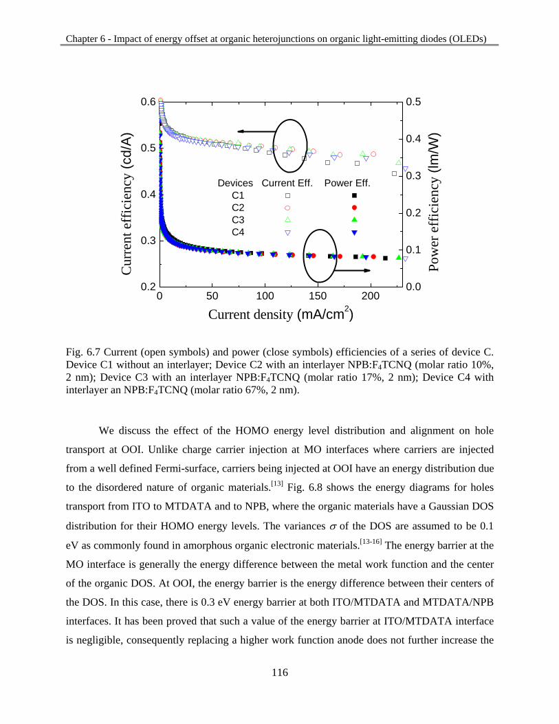
Chapter 6 - Impact of energy offset at organic heterojunctions on organic light-emitting diodes (OLEDs)
116
0 50 100 150 2000.0
0.1
0.2
0.3
0.4
0.5
0.2
0.3
0.4
0.5
0.6
Devices Current Eff. Power Eff. C1 C2 C3 C4
Pow
er e
ffic
ienc
y (lm
/W)
Current density (mA/cm2)
Cur
rent
eff
icie
ncy
(cd/
A)
Fig. 6.7 Current (open symbols) and power (close symbols) efficiencies of a series of device C. Device C1 without an interlayer; Device C2 with an interlayer NPB:F4TCNQ (molar ratio 10%, 2 nm); Device C3 with an interlayer NPB:F4TCNQ (molar ratio 17%, 2 nm); Device C4 with interlayer an NPB:F4TCNQ (molar ratio 67%, 2 nm).
We discuss the effect of the HOMO energy level distribution and alignment on hole
transport at OOI. Unlike charge carrier injection at MO interfaces where carriers are injected
from a well defined Fermi-surface, carriers being injected at OOI have an energy distribution due
to the disordered nature of organic materials.[13] Fig. 6.8 shows the energy diagrams for holes
transport from ITO to MTDATA and to NPB, where the organic materials have a Gaussian DOS
distribution for their HOMO energy levels. The variances σ of the DOS are assumed to be 0.1
eV as commonly found in amorphous organic electronic materials.[13-16] The energy barrier at the
MO interface is generally the energy difference between the metal work function and the center
of the organic DOS. At OOI, the energy barrier is the energy difference between their centers of
the DOS. In this case, there is 0.3 eV energy barrier at both ITO/MTDATA and MTDATA/NPB
interfaces. It has been proved that such a value of the energy barrier at ITO/MTDATA interface
is negligible, consequently replacing a higher work function anode does not further increase the

Chapter 6 - Impact of energy offset at organic heterojunctions on organic light-emitting diodes (OLEDs)
117
device current.[17] At this interface, due to the distribution of HOMO energy level in MTDATA,
the tail of the DOS overlaps with the ITO work function. The holes in the ITO Fermi surface can
effectively be injected into MTDATA. After the injection, the holes will through MTDATA and
relax to a mean energy <Eh>. It has demonstrated by Monte Carlo simulation that in disordered
semiconductors, <Eh> is found to be σ2 / kT away from the centre of Gaussian DOS for low
concentrations, and it moves closer to the centre at higher concentrations. As a result, compared
to hole injection at ITO/MTDATA interface, holes transport from MTDATA to NPB have to
overcome an additional energy barrier <Eh>. In our devices, It is believed that the NPB:F4TCNQ
interlayer provides an intermediate energy level to increase the overlapping of DOSs.
Fig. 6.8 A schematic of energy diagram for holes injection from ITO and transport through MTDATA to NPB. The DOS of HOMO energy levels of the organic materials have a Gaussian distribution. The variances σ of the Gaussian DOS are assumed to be 0.1 eV. The open circles are the illustration of hole carriers. They have a mean energy <Eh> away from the centre of the DOS.

Chapter 6 - Impact of energy offset at organic heterojunctions on organic light-emitting diodes (OLEDs)
118
6.5 Conclusion
In summary, it has been demonstrated that the interface doping technique can improve
charge carrier transport across organic heterojunctions in OLEDs. The power efficiency of the
BNPB blue OLED is increased by 24%. Unlike charge carrier injection at ITO/MTDATA
interface, it is found that a 0.3 eV energy offset at MTDATA/NPB still limits the charge carrier
transport. This is explained by considering a Gaussian distribution of the DOS in disordered
semiconductors. The holes in ITO can effectively be injected into the tail of the DOS of
MTDATA. As the injected holes in MTDATA relax to a mean energy <Eh> that situated away
from the centre of Gaussian DOS, the holes in MTDATA have to overcome <Eh> in order to
transport to NPB. This makes charge carrier injection at OOI less efficient than that in MO
interface. Matching energy levels in organic electronic devices is significant for optimizing
device efficiency.

Chapter 6 - Impact of energy offset at organic heterojunctions on organic light-emitting diodes (OLEDs)
119
6.6 References
[1] C. W. Tang and S. A. VanSlyke, Appl. Phys. Lett. 51, 913 (1987).
[2] L. S. Hung, C. W. Tang, and M. G. Mason, Appl. Phys. Lett. 70, 152 (1997).
[3] Y. Yuan, D. Grozea, and Z. H. Lu, Appl. Phys. Lett. 86, 143509 (2005).
[4] G. G. Malliaras and J. C. Scott, J. Appl. Phys. 85, 7426 (1999).
[5] V. I. Arkhipov, E. V. Emelianova, and H. Bassler, J. Appl. Phys. 90, 2352 (2001).
[6] P. Langevin, Ann. Chem. Phys. 28, 289 (1903).
[7] M. Pope and C. E. Swenberg, Electronic Processes in Organic Crystal. (Oxford
University Press, New York, 1982).
[8] T. v. Woudenbergh, J. Wildeman, and P. W. M. Blom, Phys. Rev. B 71, 205216 (2005).
[9] S. W. Tsang, Z. H. Lu, and Y. Tao, Appl. Phys. Lett. 90, 132115 (2007).
[10] A. Rajagopal and A. Kahn, Adv. Mater. 10, 140 (1999).
[11] W. L. Jia, X. D. Feng, D. R. Bai, Z. H. Lu, S. Wang, and G. Vamvounis, Chem. Mater.
17, 164 (2005).
[12] K. Okumoto, H. Kanno, Y. Hamada, H. Takahashi, and K. Shibata, J. Appl. Phys. 100,
044507 (2006).
[13] H. Bässler, Phys. Status Solidi B 175, 15 (1993).
[14] S. W. Tsang, S. K. So, and J. B. Xu, J. Appl. Phys. 99, 013706 (2006).
[15] P. M. Borsenberger, E. H. Magin, and J. Shi, Physica B 217, 212 (1996).
[16] H. H. Fong, K. C. Lun, and S. K. So, Chem. Phys. Lett. 353, 407 (2002).
[17] S. W. Tsang, S. C. Tse, K. L. Tong, and S. K. So, Org. Electron. 7, 474 (2006).

120
Chapter 7 Chargecarrier transport in polymeric bulkheterojunction device
7.1 Abstract The electron transport properties in various poly(3-hexylthiophene) (P3HT) and [6,6]-phenyl
C61-butyric acid methyl ester (PCBM) bulk heterojunction blend films, prepared by various
process conditions, are investigated by admittance spectroscopy (AS) at various temperatures. It
is found that the electron mobility and the dispersive transport behavior show a strong
dependence on the blend microstructure; less organized blends have orders of magnitude
reduction in the mobility and a much more dispersive transport. Using the Gaussian disordered
model (GDM), it is found that the difference of the energetic disorder of the density-of-states
(DOS) between blends plays a significant role in the observed phenomena. It is proposed that the
difference in the energetic disorder is due to different effective area of interfacial dipole at the
P3HT/PCBM heterojunctions in the various blend films.

Chapter 7 - Charge-carrier transport in polymeric bulk-heterojunction device
121
7.2 Introduction
The electron donor poly(3-hexylthiophene) (P3HT) and the electron acceptor [6,6]-
phenyl C61-butyric acid methyl ester (PCBM) are the most promising materials in making low-
cost organic photovoltaic cells by various solution processing technologies. More importantly,
they are the template for the design of new materials. Using P3HT:PCBM blend, reproducible
power conversion efficiencies of about 5% have been reported recently.[1-3] This blend consists
of an inter-penetrating network of donors and acceptors, forming bulk heterojunctions that
effectively dissociate the photo-induced excitons. In order to further increase the efficiency with
these solution-processible bulk-heterojuncion solar cells, much effort is required to understand
the corresponding impact of the interactions between the polymer donor and the fullerene
derivative acceptor in such blends.
-0.2 0.0 0.2 0.4 0.6 0.8
-10
-5
0
5
fast growthηeff = 2.6 %J
(mA
/cm
2 ) V (V)
ηeff = 4.6 %slow growth
PCBMP3HT
Fig. 7.1 J-V characteristics of devices with different growth rates of P3HT:PCBM blend. The power conversion efficiencies for a slow and a fast growth film under AM 1.5G solar irradiation (100 mW/cm2) are 4.6% and 2.6% respectively.
It is well-known that the efficiency of the bulk-heterojunction solar cells is highly
sensitive to the nanoscale organization of the bulk-heterojunction active layer, as shown in Fig.
7.1.[2,4,5] Therefore, the strategy used to cast the active layer is critical. During the casting of the

Chapter 7 - Charge-carrier transport in polymeric bulk-heterojunction device
122
active layer, the transition from liquid to solid is first accompanied by the self-organization of the
polymer followed by the phase segregation of the individual materials in the blend. As shown in ,
the degree of phase segregation is sensitive to the thermal treating after casting the active layer.
By controlling the growth rate of the active layer, one can control the domain size of the
individual material and the resulting nanoscale organization of the active layer. A high degree of
ordering obtained from a slow growth of the active layer is necessarily the main contribution to
the observed high charge-carrier mobility in bulk-heterojunction systems.[6-8]
Fig. 7.2 TEM images of P3HT:PCBM film bulk morphology before thermal annealing (a), after thermal annealing at 150oC for 30 minutes (b), and after thermal annealing at 150oC for 2 hrs (c). Adapted from Ref. [1].
Recently, it has been observed that a spontaneous transfer of a negative charge from
P3HT to C60 in bilayer structure forms an interface dipole.[9] Similarly, in P3HT:PCBM bulk-
heterojunctions, there are numerous interfaces between the individual materials. It can be
deduced that the presence of possible dipoles at these numerous interfaces will alter the charge-
carrier transport properties in the blend film.
In this Chapter, the electron transport properties in various P3HT:PCBM blends as a
function of the film microstructure will be discussed. Admittance spectroscopy (AS), a powerful
tool for probing the charge carrier dynamics, is employed to extract the electron mobility at

Chapter 7 - Charge-carrier transport in polymeric bulk-heterojunction device
123
various temperatures and to understand the physical mechanism for electron transport in the
bulk-heterojunction thin films.
7.3 Experiment
The samples fabricated in this study consist of a single active layer of P3HT:PCBM (1:1,
wt %) sandwiched between an anode (Al, 70nm) and a cathode (Mg:Ag, 10:1, 50 nm) on glass
substrates. The cathode was further covered by 50 nm of Ag used as capping layer. The metal
electrodes were thermally evaporated in vacuum at a base pressure of 10-7 Torr. The active layers
were prepared by spin-coating the blend solution in dichlorobenzene onto the Al electrode. The
organization in the active layer was controlled by varying the growth rate of the active layer.
Control of the growth rate was achieved by controlling the solution concentration, spinning
speed and thermal treatment of the active layer after spin-coating. Details of the active layer
preparation conditions are summarized in TALBE I. Samples A, B and C had the same solution
concentration and spinning condition, but different thermal treatments. The growth rate of the
active layer was decreased from sample A to sample C. In order to further decrease the growth
rate in sample D while maintaining similar film thickness, a diluted solution was used with a
smaller spinning speed. As a result, the growth rate in the different samples was in the order of
sample A > B > C > D. The thicknesses of the active layer were measured by a profilometer. The
electron mobility in P3HT:PCBM thin films was characterized by AS with an HP 4284A LRC
meter. For AS measurement, negative biases were applied at the Mg:Ag electrode. Details of the
principle and the experiment setup of AS have been discussed in Chapter 2. Although electron
injection from Mg:Ag into P3HT is possible, the injected electrons will be rapidly transferred to
the PCBM molecules which has a lower lowest-unoccupied molecular orbital (LUMO) energy
level. Prior to the charge carrier mobility measurements, any absorbed ambient effect during
sample transfer or residual solvent was eliminated by moderately heating the sample at 50 oC for
24 hours inside a temperature regulated cryostat with a base pressure of 10-6 Torr.

Chapter 7 - Charge-carrier transport in polymeric bulk-heterojunction device
124
sample soln concentration spinning condition thermal treatment thickness
A 112 mg / mL 1000 rpm (60s) baked 200oC (30mins) 1.20 μm
B 112 mg / mL 1000 rpm (60s) baked 100oC (30mins) 1.16 μm
C 112 mg / mL 1000 rpm (60s) naturally dried for 24 hrs 1.16 μm
D 42.5 mg / mL 300 rpm (60s) naturally dried for 24 hrs 1.50 μm
Table 7.1 Summary of preparation condition of the P3HT:PCBM (1:1 wt%) blends
7.4 Results and discussion
7.4.1 Electron mobility measured by admittance spectroscopy Fig. 7.3 shows the typical capacitance vs frequency characteristics of the different
samples measured by AS. A minimum capacitance Cmin at a certain frequency is found in
samples B, C, and D. This feature corresponds to the space charge effect in the bulk of the
material.[10,11] It also proves that a quasi-Ohmic contact is formed at the Mg:Ag/PCBM
interface.[12] The electron mobility μe can be effectively extracted from the measured
capacitance. Briefly, if Cmin occurs at higher frequency it indicates a higher charge carrier
mobility. Therefore, μe increases from sample B to sample D, corresponding to a fast and a slow
growth rate respectively. Moreover, the degree of charge carrier mobility dispersion can be
revealed by considering the ratio of Cmin/Cgeo, where Cgeo is the geometrical capacitance of the
sample. In the case of non-dispersive transport, Cmin/Cgeo = 0.75. [10,11] The value of Cmin/Cgeo
increases for more dispersive transport. For highly dispersive transport the capacitance minimum
vanishes. As shown in Fig. 7.3, there is no capacitance minimum observed in sample A. The
value of Cmin/Cgeo deceases from 0.98 in sample B to 0.92 in sample D, which suggests that the
electron transport becomes less dispersive as the growth rate of the active layer decreases. It is
worth considering that the dispersive transport behavior can originate from the presence of trap
states, or from the disordered properties of the transporting sites, both positional and energetic.
However, since the samples are prepared with the same batch of materials, the variation of bulk
trap states in different samples is safely excluded. Furthermore, it has been demonstrated that a
slower growth rate of the active layer leads to a more ordered P3HT:PCBM film.[3,5] Therefore,

Chapter 7 - Charge-carrier transport in polymeric bulk-heterojunction device
125
the difference of the disordered properties between samples is attributed to the variation of the
observed electron transport behavior.
102 103 104 1050.90
1.00
1.10
0.98
1.00
1.02
1.00
1.10
1.00
1.10
1.20
Frequency (Hz)
Cmin / Cgeo= 0.92
Cmin / Cgeo= 0.95
Cmin / Cgeo= 0.98
(d)
(c)
(b)
C /
Cge
o
(a)
Fig. 7.3 Measured capacitance vs frequency characteristics of sample (a) A at T = 263 K and F = 2.0 x 10⁵ V/cm ; (b) B at T = 263 K and F = 2.0 x 10⁵ V/cm ; (c) C at T = 263 K and F = 2.0 x 10⁵ V/cm; (d) D at T = 270 K and F = 1.3 x 10⁴ V/cm. The capacitance C is normalized to the geometrical capacitance Cgeo of individual sample.
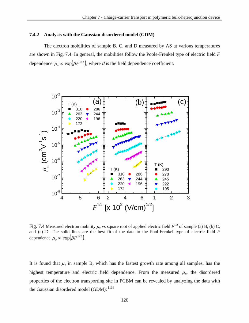
Chapter 7 - Charge-carrier transport in polymeric bulk-heterojunction device
126
7.4.2 Analysis with the Gaussian disordered model (GDM) The electron mobilities of sample B, C, and D measured by AS at various temperatures
are shown in Fig. 7.4. In general, the mobilities follow the Poole-Frenkel type of electric field F
dependence ( )2/1exp Fe βμ ∝ , where β is the field dependence coefficient.
4 5 610-8
10-7
10-6
10-5
10-4
10-3
10-2
2 4 6 1 2 3
T (K) 310 286 263 244 220 196 172
μ e (cm
2 V-1s-1
)
F1/2 [x 102 (V/cm)1/2]
(c)(b)
T (K) 310 286 263 244 220 196 172
(a)
T (K) 290 270 245 222 195
Fig. 7.4 Measured electron mobility μe vs square root of applied electric field F1/2 of sample (a) B, (b) C, and (c) D. The solid lines are the best fit of the data to the Pool-Frenkel type of electric field F dependence ( )2/1exp Fe βμ ∝ .
It is found that μe in sample B, which has the fastest growth rate among all samples, has the
highest temperature and electric field dependence. From the measured μe, the disordered
properties of the electron transporting site in PCBM can be revealed by analyzing the data with
the Gaussian disordered model (GDM): [13]

Chapter 7 - Charge-carrier transport in polymeric bulk-heterojunction device
127
⎟⎟
⎠
⎞
⎜⎜
⎝
⎛
⎥⎥⎦
⎤
⎢⎢⎣
⎡Σ−⎟
⎠⎞
⎜⎝⎛
⎥⎥⎦
⎤
⎢⎢⎣
⎡⎟⎠⎞
⎜⎝⎛−= F
kTC
kTTE 2
22
inf exp32exp),( σσμμ
(7.1)
where μinf is a prefactor, σ is the energetic disorder parameter that can be understood as the
width of the Gaussian density-of-state (DOS), Σ is the positional disorder parameter, and C is a
constant. By extrapolating the measured μe to zero field, σ can be obtained from the plot of the
zero field mobility μ0,T vs 1/T2 as shown in Fig. 7.5a. On the other hand, Σ can be extracted by
plotting β vs 1/T2 as shown in Fig. 7.5b. The extracted disorder parameters for different samples
are summarized in Table 7.2.
0 10 20 30 4010-14
10-12
10-10
10-8
10-6
10-4
10-2
100
0 10 20 30 400
5
10
15
20
25
30
(b)
sample B sample C sample D
μ 0,T (c
m2 V
-1s-1
)
(1000/T)2 (K-2)
(a)
β x
103 [(
V/c
m)-1
/2)]
(1000/T)2 (K-2)
Fig. 7.5 (a) The zero-field mobility μ0,T extrapolated from the measured μe in Fig. 7.4 vs 1 / T2 of
different samples. (b) The corresponding field dependence coefficient β vs 1 / T2. The solid lines are the
best fits to the data at temperature T > 220K.

Chapter 7 - Charge-carrier transport in polymeric bulk-heterojunction device
128
Sample μinf (cm
2V
-1s-1
) σ (meV) C (V/cm)-1 Σ
B 0.041 124 4.53 x 10⁻⁴ 2.63 C 0.19 106 2.12 x 10⁻⁴ 2.06 D 0.30 82 3.93 x 10⁻⁴ 1.58
Table 7.2 Extracted GDM parameters of different samples from the measured electron mobility μe in
Fig. 7.5.
As expected, the largest positional disorder parameter Σ is found in sample B and the
smallest in sample D. A more organized film of P3HT:PCBM blend can be formed from a
slower growth rate of the active layer. Although it is generally believed that such improved
ordering is only a result of the increase of crystalline packing of P3HT, there is no doubt that
more PCBM will also pack together to retain a constant effective volume. This has been proved
by the observed phase segregation between P3HT and PCBM measured by AFM.[4] Surprisingly,
there is a large difference in the energetic disorder parameter σ between different samples. As
depicted in Eq. (7.1), the low field mobility is mainly determined by the μinf and σ. Taking
sample B and D as an example, μinf in sample B is about one order of magnitude lower than that
in sample D. However, a large value of σ in sample B attributes to more than two orders of
magnitude reduction in mobility. Extensive experimental studies on carrier transport properties
in polymers doped with hole-transporting molecules have been reported by Borsenberger and co-
workers, with detailed discussion of μinf and σ in different polymer hosts.[14,15] The prefactor μinf
depends on the inter-site distance R and wave-function decay constant α as:
( )RR αμ 2exp2inf −∝ (7.2)
Owning to the energy difference of the transporting sites in P3HT and PCBM, the wave-function
overlap is larger between PCBM molecules. Moreover, in a less organized blend that with
smaller degree of phase segregation, more PCBM molecules are mixed with the P3HT polymers
which increases the inter-molecular distance. As a result, a smaller α and a larger R in less
organized blend attribute to a smaller μinf. Despite this spatial effect, it is found that the increased
Chapter 7 - Charge-carrier transport in polymeric bulk-heterojunction device
129
energetic disorder of PCBM in the less organized blend plays an important role for the reduction
in electron mobility.
7.4.3 Impact of dipole at P3HT/PCBM interface on electron transport
The variation of σ in different blend films can be explained by considering the presence
of interface dipoles between P3HT and PCBM. The dipolar effect on the energy profile of the
DOS and the charge-carrier transport in a disordered media was originally proposed by
Dieckmann and Young under the framework of the GDM.[16,17] The energetic disorder parameter
takes into account both the dipole-induced disorder σd and the van der Waals interactions
between molecules σvdw, i.e.:
222vdwd σσσ += (7.3)
The additional σd broadens the Gaussian DOS which depends on the amount and the orientation
of the dipole moments in the system.[17] It has been recently reported that there exists an interface
dipole between P3HT and C60 by photoemission study.[9] Assuming the magnitude of the dipole
at the P3HT/PCBM interface in different blend films are comparable, it is proposed that the
origin of the difference of σd between samples with slower and faster growth rate of the active
layer is due to the variation of the interfacial area of the heterojunctions as illustrated Fig. 4.

Chapter 7 - Charge-carrier transport in polymeric bulk-heterojunction device
130
Fig. 7.6 An illustration of the phase segregation of P3HT:PCBM for slow and fast growth rate of the
active layer. Interface dipoles are formed at P3HT/PCBM heterojunctions.
Less phase segregation between P3HT and PCBM is expected for the film grown faster.
The area of the P3HT/PCBM interface, and therefore the number of interface dipoles are larger
inside this blend. Moreover, as the PCBM phase is smaller, the injected electrons have higher
probability to experience the interface dipole effect during the multi-directional hopping process.
This attributes to a larger overall energetic disorder σ for the sample having a faster growth rate
of the active layer. A larger σ reduces the electron mobility and results in much more dispersive
transport behavior. In other words, in the absence of dipoles at the P3HT/PCBM interface, the
difference in charge carrier mobility between samples are mainly determined by the prefactor μinf
and the positional disorder parameter Σ, which depends on the degree of the self-organization of
samples. However, the presence of dipoles at the P3HT/PCBM interface additionally increases
the energetic disorder parameter σ which further reduces the charge carrier mobility. The
contribution of the dipole disorder σd also depends on the degree of the self-organization of the
samples; a larger σd is expected in less organized blends that have larger P3HT/PCBM interface
area.

Chapter 7 - Charge-carrier transport in polymeric bulk-heterojunction device
131
7.5 Conclusion
In conclusion, the electron transport properties in P3HT:PCBM (1:1) blend films have
been studied by admittance spectroscopy at various temperatures. It is found that both the
electron mobility and the dispersive transport behavior depend strongly on the growth rate of the
active layer. According to the results of the measured electron mobility of different samples at
various temperatures, the electron mobility is mainly determined by the variation of the energetic
disorder, rather than by the spatial distribution of the transporting sites in PCBM. This is
proposed to be a result of the variation of the induced-dipole disorder at the P3HT/PCBM
interfaces within the blend films. A faster growth rate with less phase segregation between P3HT
and PCBM leads to larger effective area of interfacial dipole at the P3HT/PCBM heterojunctions
which impede electron transport in the blend films by increasing the energetic disorder of the
density-of-states.

Chapter 7 - Charge-carrier transport in polymeric bulk-heterojunction device
132
7.6 References [1] W. Ma, C. Yang, X. Gong, K. Lee, and A. J. Heeger, Adv. Funct. Mater. 15, 1617
(2005).
[2] G. Li, V. Shrotriya, J. Huang, Y. Yao, T. Moriarty, K. Emery, and Y. Yang, Nat Mater 4,
864 (2005).
[3] Youngkyoo Kim, Steffan Cook, Sachetan M. Tuladhar, Stelios A. Choulis, Jenny Nelson,
James R. Durrant, Donal D. C. Bradley, Mark Giles, Iain McCulloch, Chang-Sik Ha, and
Moonhor Ree, Nat Mater 5, 197 (2006).
[4] V. Shrotriya, Y. Yao, G. Li, and Y. Yang, Appl. Phys. Lett. 89, 063505 (2006).
[5] C.-W. Chu, H. Yang, W.-J. Hou, J. Huang, G. Li, and Y. Yang, Appl. Phys. Lett. 92,
103306 (2008).
[6] R. Pacios, J. Nelson, D. D. C. Bradley, and C. J. Brabec, Appl. Phys. Lett. 83, 4764
(2003).
[7] S. A. Choulis, J. Nelson, Y. Kim, D. Poplavskyy, T. Kreouzis, J. R. Durrant, and D. D. C.
Bradley, Appl. Phys. Lett. 83, 3812 (2003).
[8] J. Huang, G. Li, and Y. Yang, Appl. Phys. Lett. 87, 112105 (2005).
[9] W. Osikowicz, M. P. de Jong, and W. R. Salaneck, Adv. Mater. 19, 4213 (2007).
[10] S. W. Tsang, S. K. So, and J. B. Xu, J. Appl. Phys. 99, 013706 (2006).
[11] H. C. F. Martens, H. B. Brom, and P. W. M. Blom, Phys. Rev. B 60, R8489 (1999).
[12] S. W. Tsang, S. C. Tse, K. L. Tong, and S. K. So, Org. Electron. 7, 474 (2006).
[13] H. Bässler, Phys. Status Solidi B 175, 15 (1993).
[14] P. M. Borsenberger, J. Appl. Phys. 68, 5188 (1990).
[15] J. A. Sinicropi, J. R. Cowdery-Corvan, E. H. Magin, and P. M. Borsenberger, Proc. SPIE
2850, 202 (1996).
[16] A. Dieckmann, H. Bassler, and P. M. Borsenberger, The Journal of Chemical Physics 99,
8136 (1993).
[17] R. H. Young, Philos. Mag. B 72, 435 (1995).

Chapter 8 Conclusions and Future Work
8.1 Conclusions
This thesis reports on research progress in carrier injection and transport across organic
heterojunctions (OHs). A theoretical model of carrier injection across an OH has been proposed
to explain several new experimental findings. The model has been validated against
measurements of a series of single carrier OH devices at various applied electric field and
temperatures. The impact OH on OLED performance is also demonstrated. The major
conclusions of the thesis are summarized as follow:
In Chapter 3, an injection model for OHs which includes the distribution of carriers at the
injecting side of the interface is presented. This model shows that the main contribution to the
injection current is from carriers at the peak of the Gaussian density-of-states (DOS) rather than
at the Fermi level. In addition, charge carrier dependent barrier height, vφ , is proposed based on
energy level re-alignment of the Fermi level. The model is verified by the excellent agreement
with the experimental results of the current density – voltage (J-V) characteristics of an OH
device for various temperatures over a wide range of electrical field. The results show that
dynamic change in carrier concentration and DOS energy alignment at the OH play significant
roles in the performance of organic heterojunction devices.
In Chapter 4, an escape probability function, wesc, based on the total hopping frequencies
at both sides of the organic heterojunction is formulated. It is shown that the injection current at
low temperature is greatly increased and pinned by an extremely low density (1010 cm-3) of deep
trap states. As a result, the injection current across a heterojunction with a larger injection barrier
has a smaller temperature dependence. The calculation results are in good agreement with the
experimental results of heterojunction devices with barrier heights ranging from 0.4 eV – 1.0 eV.
133
It is also demonstrated that the carrier mobility in a single layer device shows similar
temperature dependence. This strongly supports the view that the small number of deep trap
states originate from the bulk material instead of only from the interface. This study also
suggests that, in the presence of the deep trap states, simply extracting the barrier height from the
Arrhenius plot is inappropriate.
In Chapter 5, both experiment and theoretical simulation, show that charge transport in a
double layer device is limited by a potential barrier at the organic-organic heterojunction. It is
demonstrated that the injection barrier at the OH can be effectively modulated by introducing a
thin (2 nm) p-doped interlayer at the heterojunction. Carrier injection across MTDATA/NPB
heterojunction can be easily modulated by inclusion of a doped interlayer at the junction: a
NPB:F4-TCNQ interlayer for increasing hole current or a MTDATA:F4-TCNQ interlayer for
decreasing hole current. A change in the quasi Fermi level upon doping together with energy
level alignment at the heterojunctions were proposed as the underling physics principles to
explain the observed phenomena. The junction doping technique provides a promising
alternative pathway to modulate electron or hole current in organic electronic devices using
commonly available organic semiconductor molecules.
In Chapter 6, interface doping is demonstrated as an alternative engineering way to
enhance charge carrier injection across organic heterojunctions in OLEDs. The power efficiency
of the BNPB blue OLED is increased by 24% through interface doping to eliminate the
heterojunction barrier. Unlike charge carrier injection at ITO/MTDATA interface, it is found that
a 0.3 eV energy offset at MTDATA/NPB still limits the charge carrier transport. This is
explained by considering a Gaussian distribution of the DOS in disordered semiconductors. The
holes in ITO can effectively be injected into the tail of the DOS of MTDATA. As the injected
holes in MTDATA relax to a mean energy <Eh> that is situated away from the centre of the
Gaussian DOS, the holes in MTDATA have to overcome <Eh> in order to transport to NPB. This
makes charge carrier injection at an OOI less efficient than that at a MO interface. Matching
energy levels in organic electronic devices is significant for optimizing device efficiency.
134

In Chapter 7, the electron transport properties in P3HT:PCBM (1:1) blend films are
studied by using admittance spectroscopy at various temperatures. It is found that the electron
mobility and the dispersive transport behavior depend strongly on the growth rate of the blend
films. According to the results of the measured electron mobility of different samples at various
temperatures, the electron mobility is mainly determined by the variation of the energetic
disorder, rather than by the spatial distribution of the transporting sites in PCBM. This is
explained as a result of the variation of the induced-dipole disorder at the P3HT/PCBM
interfaces within the blend films. A faster growth rate with less phase segregation between P3HT
and PCBM leads to larger effective area of interfacial dipoles at the P3HT/PCBM
heterojunctions, and thus the electron transport in the blend films is decreased by the increased
energetic disorder of the density-of-states.
8.2 Future Work
Chapter 3 shows that the carrier concentration at the organic heterojunction can be
extracted by a steady state simulation. Ultimately, the carrier concentration can be obtained
experimentally by the capacitance-voltage method as developed for the heterojunctions in
inorganic semiconductors.[1] Therefore, extracting barrier height and calculating the injection
current at the organic heterojunctions can be done without the need of knowing the carrier
mobility of each material.
In Chapter 4, the measured carrier mobility of a single carrier device is shown (Fig. 4.14)
to have a large discrepancy with the model proposed by Arkhipov et al. at low temperature. It is
believed that the measured temperature dependence of the carrier mobility is a common feature
in organic semiconductors as has been reported by several groups.[2,3] The most critical reason
for the discrepancy is the formulation of the effective transport energy Etr which is assumed that
the most possible jumps are energetically upward.[4] However, downward jumps may be
dominated, especially the thermal energy is not enough for upward jump or there is a large
energy barrier. This is already demonstrated by considering the total hopping frequency and
135

136
available hopping sites at both sides of the interface in the studies in Chapter 4. This suggests
that the formulation of the effective transport energy Etr has to be revised.
In addition, shown in Chapter 7, the effect of heterojunction dipoles on electron transport
in a bulk heterojunction (P3HT:PCBM) film is presented. More detailed study on such effect can
be conducted by replacing P3HT with another “inert” polymer (e.g. polycarbonate (PC)).
Therefore, there should be an absence of dipole effect in the PC:PCBM system, and the dipole
effect on carrier transport can be more clearly differentiated. Furthermore, it is also interesting to
investigate the hole transporting properties of the P3HT:PCBM blend. This information should
be useful for understanding the improved performance of the OPV cells.
8.3 References
[1] Y. Nemirovsky, G. Gordon, and D. Goren, J. Appl. Phys. 84, 1113 (1998).
[2] T. Kreouzis, D. Poplavskyy, S. M. Tuladhar, M. Campoy-Quiles, J. Nelson, A. J.
Campbell, and D. D. C. Bradley, Phys. Rev. B 73, 235201 (2006).
[3] H. Sirringhaus, P. J. Brown, R. H. Friend, M. M. Nielsen, K. Bechgaard, B. M. W.
Langeveld-Voss, A. J. H. Spiering, R. A. J. Janssen, E. W. Meijer, P. Herwig, and D. M.
de Leeuw, Nature 401, 685 (1999).
[4] V. I. Arkhipov, E. V. Emelianova, and G. J. Adriaenssens, Phys. Rev. B 64, 125125
(2001).

Appendix A Experimental results of carrier mobility measured by time‐of‐flight (TOF) technique
A.1 Average hole mobility of MTDATA
Device structure: ITO / MTDATA (3.00 μm) /Al (30 nm)
400 600 800 1000 1200
10-5
10-4
10-3
0 20 40 60 80
Pho
tocu
rrne
t (a.
u.)
Time (μs)
μ dc (c
m2 V
-1s-1
)
F1/2 [(V/cm)1/2]
Temperature (K) 335.8 316.3 299.1 290.1 280.4 270.3 260.4 250.6 241.6 232.4
T = 290 KF = 3.14 x 10⁵ V/cm
Fig. A.1 The field dependent μdc of MTDATA extracted by TOF vs the square root of the applied electric field F1/2 at different temperatures. The solid lines are the best line fits to the data. The inset shows the typical transient current measured by TOF.
137

8 12 16 20 241
2
3
4
5
8 12 16 20 24
10-7
10-6
10-5
10-4
β x
103 [(
V/c
m)-1
/2]
(σ/kT)2
(b)
μ 0,T (c
m2 V
-1s-1
)
(1000/T)2 (K-2)
(a)
Fig. A.2 (a) The zero field mobility T,0μ vs ; (b) the corresponding field dependent 2/1 T β vs
. The energetic 2/1 T σ and the positional Σ disorder parameters of MTDATA can be extracted from these plots as listed in Table A.1. The solid lines are the best line fits to the data.
138

A.2 Average hole mobility of NPB
Device Structure: ITO / NPB (3.5 μm) /Al (30nm)
200 400 600 80010-5
10-4
10-3
10-2
0 2 4 6 8
Pho
tocu
rrent
(a.u
.)
Time (μs)
Temperature (K) 333 325 316 306 300 291 280 269 259 249 239 228
μ dc (c
m2 V
-1s-1
)
T = 275 KF = 3.19 x 10⁵ V/cm
F1/2 [(V/cm)1/2]
Fig. A.3 The field dependent μdc of NPB extracted by TOF vs the square root of the applied electric field F1/2 at different temperatures. The solid lines are the best line fits to the data. The inset shows the typical transient current measured by TOF.
139
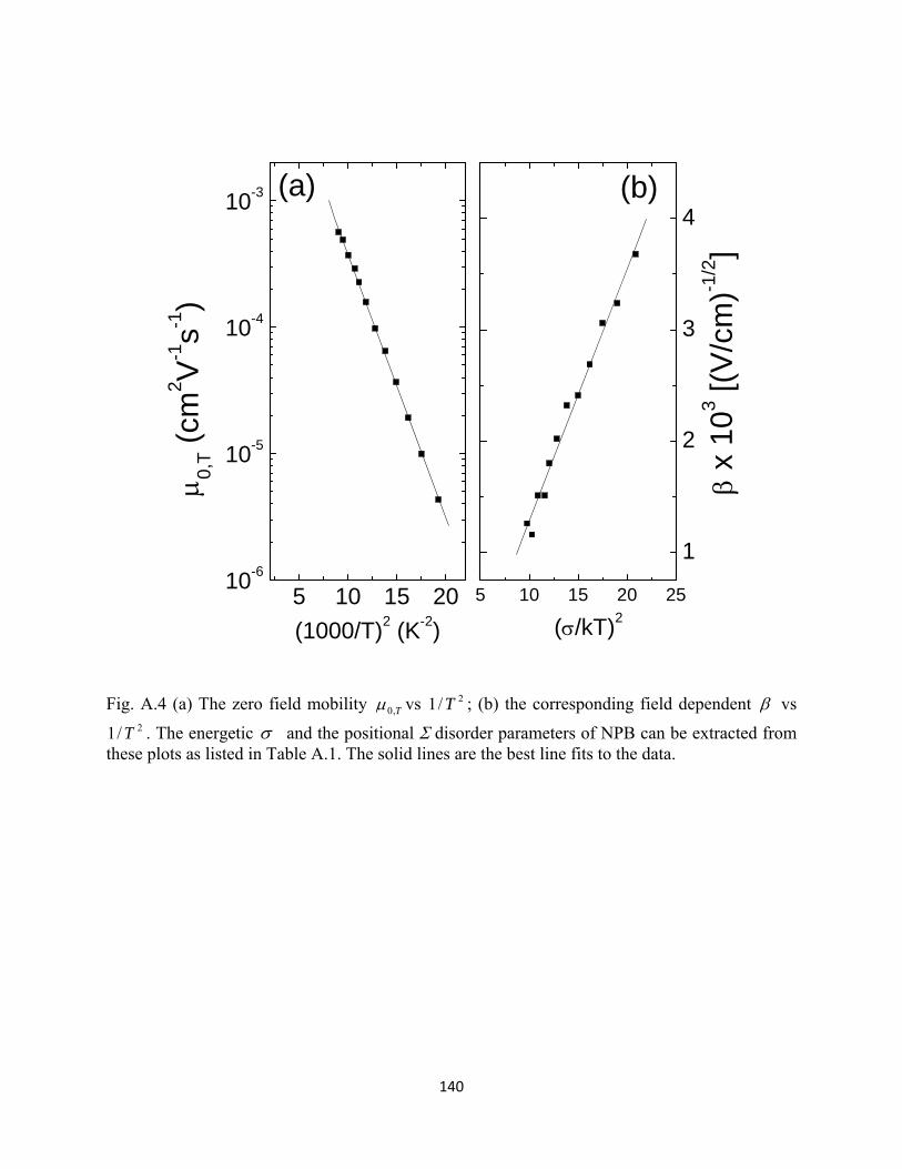
5 10 15 2010-6
10-5
10-4
10-3
5 10 15 20 25
1
2
3
4(b)
μ 0,T (c
m2 V
-1s-1
)
(1000/T)2 (K-2)
(a)
β x
103 [(
V/c
m)-1
/2]
(σ/kT)2
Fig. A.4 (a) The zero field mobility T,0μ vs ; (b) the corresponding field dependent 2/1 T β vs
. The energetic 2/1 T σ and the positional Σ disorder parameters of NPB can be extracted from these plots as listed in Table A.1. The solid lines are the best line fits to the data.
140

A.3 Average hole mobility of TPD
Device Structure: ITO / TPD (4.2 μm) /Al (30nm)
200 400 600 800
10-4
10-3
10-2
0 2 4 6 8
Phot
ocur
rnet
(a.u
.)
Time (μs)
Temperature (K) 307 294 278 263 249 235 222 208
μ dc (c
m2 V
-1s-1
)
F1/2 (V/cm)1/2
T = 278 KF = 1.43 x 10⁵ V/cm
Fig. A.5 The field dependent μdc of TPD extracted by TOF vs the square root of the applied electric field F1/2 at different temperatures. The solid lines are the best line fits to the data. The inset shows the typical transient current measured by TOF.
141

5 10 15 20 251
2
3
4
5 10 15 20 25 30
10-5
10-4
10-3
β x
103 [(
V/c
m)-1
/2]
(σ/kT)2
(b)μ 0,
T (cm
2 V-1s-1
)
(1000/T)2
(a)
Fig. A.6 (a) The zero field mobility T,0μ vs ; (b) the corresponding field dependent 2/1 T β vs
. The energetic 2/1 T σ and the positional Σ disorder parameters of TPD can be extracted from these plots as listed in Table A.1. The solid lines are the best line fits to the data.
142

A.4 Average hole mobility of TCTA
Device Structure: ITO / TCTA (4.5 μm) /Al (30nm)
200 400 600 800 100010-6
10-5
10-4
10-3
10-2
10-1
0 2 4 6 8 10P
hoto
curr
ent (
a.u.
)
Time (μs)
Temperature (K) 301 287 270 255 237 225 212
μ dc (c
m2 V
-1s-1
)
F1/2 [(V/cm)1/2]
T = 270 KF = 1.8 x 10⁵ V/cm
Fig. A.7 The field dependent μdc of TCTA extracted by TOF vs the square root of the applied electric field F1/2 at different temperatures. The solid lines are the best line fits to the data. The inset shows the typical transient current measured by TOF.
143

12 14 16 18 20 2210-7
10-6
10-5
10-4
10-3
10-2
15 20 25 30 35 400
1
2
3
4
5
6(b)
μ 0,
T (cm
2 V-1s-1
)
(1000/T)2 (K-2)
(a)
β x
103 [(
V/c
m)-1
/2]
(σ/kT)2
Fig. A.8 (a) The zero field mobility T,0μ vs ; (b) the corresponding field dependent 2/1 T β vs
. The energetic 2/1 T σ and the positional Σ disorder parameters of TCTA can be extracted from these plots as listed in Table A.1. The solid lines are the best line fits to the data.
144

A.5 Disorder parameters extracted by Gaussian-Disorder-Model (GDM)
σ (eV) Σ C μinf (cm2V-1s-1)
MTDATA 0.093 2.15 2.30 x 10⁻⁴ 3.95 x 10⁻³
NPB 0.090 2.08 2.27 x 10⁻⁴ 4.73 x 10⁻²
TPD 0.080 2.57 3.15 x 10⁻⁴ 7.42 x 10⁻²
TCTA 0.112 3.70 1.74 x 10⁻⁴ 11.0
Table A.1 Extracted GDM parameters for MTDATA, NPB, TPD, and TCTA.
145

Appendix B Publications
B.1 Publications resulting from this thesis:
1. S. W. Tsang, M. W. Denhoff, Y. Tao, Z. H. Lu, “Temperature dependence of carrier injection across organic heterojunction”, Phys. Rev. B (submitted)
2. S. W. Tsang, N. Drolet, S. C. Tse, Y. Tao, and Z. H. Lu, “Heterojunction-dipole effect on electron mobility in poly(3-hexylthiophene) and [6,6]-phenyl C61-butyric acid methyl ester blend”, Adv. Mater. (submitted)
3. N. Drolet, S. W. Tsang, S. C. Tse, Y. Tao, and Z. H. Lu, “Admittance Spectroscopy
Technique for the Determination of Charge Mobility in Polymer/Fullerene Thin Films used in Solar Cells” (In preparation)
4. S. W. Tsang, M. W. Denhoff, Y. Tao, Z. H. Lu, “Charge-carrier induced barrier-height reduction at organic heterojunction”, Phys. Rev. B 78, 081301(R) (2008)
5. S. W. Tsang, Y. Tao, Z. H. Lu, “Engineering carrier transport across organic
heterojunctions by interface doping”, Appl. Phys. Lett. 90, 132115 (2007)
B.2 Other related publications: 6. Z. B. Wang, M. G. Helander, S. W. Tsang, Z. H. Lu, “Abnormal charge injection bebavior at
metal-organic interfaces” Phys. Rev. B 78, 193303 (2008)
7. P. F. Xia, X. J. Feng, J. Lu, S. W. Tsang, R. Movileanu, Y. Tao, and M. S. Wong, “Donor-Acceptor Oligothiophenes as Low Optocal Gap Chromophores for Photovoltaic Application”, Adv. Mater. (2008) (in press)
8. K. L. Tong, S. W. Tsang, K. K. Tsung, S. C. Tse, and S. K. So, “Hole transport in molecularly doped naphthyl diamine”, J. Appl. Phys. 102, 093705 (2007)
9. Y. Y. Yuan, S. Han, S. W. Tsang, D. Grozea, J. Zhang, Z. H. Lu, “Organic-fullerene composite anode structures for organic light-emitting diodes”, Proc. SPIE 6333, 63331S (2006)
10. S. C. Tse, S. W. Tsang, and S. K. So, "Nearly ohmic injection contacts from PEDOT:PSS to phenylamine compounds with high ionization potentials", Proc. SPIE 6333, 63331P (2006)
146
11. S. W. Tsang, S. C. Tse, K. L. Tong and S. K. So, “Direct determination of carrier mobility of OLED materials by admittance spectroscopy”, Proc. SPIE 6333, 633313 (2006)
12. S. C. Tse, S. W. Tsang, and S. K. So, “PEDOT:PSS polymeric conducting anode for small organic transporting molecules in dark injection experiments”, J. Appl. Phys. 100, 063708 (2006)
13. S. W. Tsang, S. C. Tse, K. L. Tong and S. K. So, “PEDOT:PSS polymeric conducting anode for admittance spectroscopy”, Org. Electron. 7, 474 (2006)
14. S. W. Tsang, S. K. So, and J. B. Xu, “Application of admittance spectroscopy to evaluate carrier mobility in organic transport materials”, J. Appl. Phys. 99, 013706 (2006)
B.3 Conference presentations
Invited talk:
1. S. W. Tsang, S. C. Tse, K. L. Tong and S. K. So, “Direct determination of carrier mobility of OLED materials by admittance spectroscopy”, SPIE Optics and Photonics 2006, San Diego, 6333-39
2. S. K. So, S. C. Tse, S. W. Tsang, “Using PEDOT:PSS to Form Nearly Ohmic Hole Injection Contact to Small-molecule Organic Charge Transporters”, MRS 2006 Fall meeting, Boston, United States, Symposium S14.1
Poster presentation:
1. S. W. Tsang, M. W. Denhoff, Y. Tao, Z. H. Lu, “Charge carrier injection across organic heterojunction”, MRS 2008 Organic Microelectronics and Optoelectronics Workshop IV, San Francisco, United States, P33
2. N. Drolet, S. W. Tsang, S. C. Tse, Y. Tao, and Z. H. Lu, “A comprehensive study on the impact of film morphology, crystallinity, and carrier mobility on organic solar cell performance”, MRS 2008 Organic Microelectronics and Optoelectronics Workshop IV, San Francisco, United States, P10
147

148
3. S. W. Tsang, Y. Tao, and Z. H. Lu, “Engineering Carrier Transport Across Organic Heterojunctions by Interface Doping”, MRS 2007 Spring meeting, San Francisco, United States, Symposium O3.6
4. S. C. Tse, S. W. Tsang, and S. K. So, "Nearly ohmic injection contacts from PEDOT:PSS to phenylamine compounds with high ionization potentials", SPIE Optics and Photonics 2006, San Diego, 6333-63
5. Y. Y. Yuan, S. Han, S. W. Tsang, D. Grozea, J. Zhang, Z. H. Lu, “Organic-fullerene composite anode structures for organic light-emitting diodes”, SPIE Optics and Photonics 2006, San Diego, 6333-66
6. S. W. Tsang, S. K. So, “Feasibility of Admittance Spectroscopy in Evaluating Carrier Mobility in Organic Charge Transporting Materials”, MRS 2005 Fall meeting, Boston, United States, Symposium D10.3
7. S. W. Tsang, A. Jin, J. B. Xu, “Negative Capacitance in Copper Phthalocyannie (CuPc) organic semiconductor”, The Sixth Functional π-Electron Systems, Cornell University, United States (2004)
Recommended