1
Characterization of Contact Electromechanics through
Capacitance-Voltage Measurements and Simulations
E. K. Chan, K. Garikipati, and R. W. Dutton, Fellow, IEEE
CISX 305, Center for Integrated Systems
Stanford University, Stanford, CA 94305-4075
Email: [email protected] Tel: (650) 723-1482 Fax: (650) 725-7731
Abstract - Electrostatically actuated polysilicon beams fabricated in the MUMPs process are
studied, with an emphasis on the behavior when the beam is in contact with an underlying silicon
nitride dielectric layer. Detailed 2D electromechanical simulations, including the mechanical
effects of stepups, stress-stiffening and contact, as well as the electrical effects of fringing fields
and finite beam thickness, are performed. Comparisons are made to quasi-2D and 3D simulations.
Pull-in voltage and capacitance-voltage measurements together with 2D simulations are used to
extract material properties. The electromechanical system is used to monitor charge buildup in the
nitride which is modeled by a charge trapping model. Surface effects are included in the simulation
using a compressible-contact-surface model. Monte Carlo simulations reveal the limits of
simulation accuracy due to the limited resolution of input parameters. [128]
Index terms – Electromechanical, contact, charge, surface, material properties, electrostatic
2
I. I NTRODUCTION
Electrostatically actuated beams (Fig. 1a) are widely used and studied in the
microelectromechanical systems (MEMS) community. Such beams are used as switches [1] and
resonators [2], [3], and for extracting material properties [4]-[6], [18]. One-dimensional (1D),
quasi-two-dimensional (quasi-2D) and three-dimensional (3D) simulations of various accuracies
and sophistication have been used to help understand and characterize these beams and devices [5]-
[9]. Currently, full 3D simulations consume substantial computing resources and time, making
them infeasible for parameter extraction procedures which require the solutions of many variations
of a given system about a nominal set of parameters. This is especially significant near pull-in
where convergence is not easily achieved through the relaxation coupling algorithm employed by
most electrostatics-elastostatics simulators. Thus, quasi-2D models (only one mechanical degree-
of-freedom per node) implemented in Matlab [5], [6], [8] which take advantage of the
predominantly 2D behavior of these beams have been used. However, the rather ad hoc correction
factors required to account for compliant stepup boundary conditions are usually specific to the
range of beam dimensions being studied. In addition, contact algorithms are difficult to implement.
Simulation results are presented here using a more detailed 2D mechanical model in AbaqusTM [11]
which allows accurate simulation of the effects of stepups, finite deformation (large rotations and
stress stiffening) and compressible or “softened” contact surfaces. The effects of fringing fields
and finite conductor thickness are included in the electrostatics model. Results are compared for
quasi-2D, 2D and 3D simulations of the simple case of an ideal fixed-fixed beam loaded
electrostatically which can be solved by all three methods, at least up until pull-in.
The behavior of the system is studied for the case when the beam is in contact with the
dielectric that coats the bottom electrode — a mode of operation important to capacitive microwave
3
switches [1]. The electromechanical structures fabricated in the Multi-User MEMS Process
(MUMPs) of the Microelectronics Center of North Carolina (MCNC) [10] are strongly influenced
by charge in the nitride. This phenomenon is exploited to monitor charge buildup over time which
is modeled by a charge trapping model. In addition, even after a part of the beam contacts the
nitride, surface effects cause the electrical gap between that part of the beam and bottom electrode
to vary with applied voltage. A compressible-contact-surface model captures these effects in the
Abaqus simulations thus improving the fit to measured capacitance-voltage curves. Monte Carlo
simulations then reveal the limits of simulation accuracy due to the limited precision of extracted
parameters.
II. SIMULATION MODEL
A. Overview
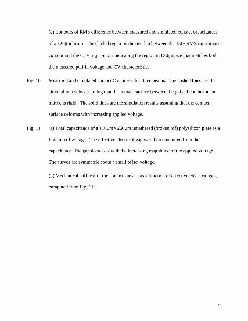
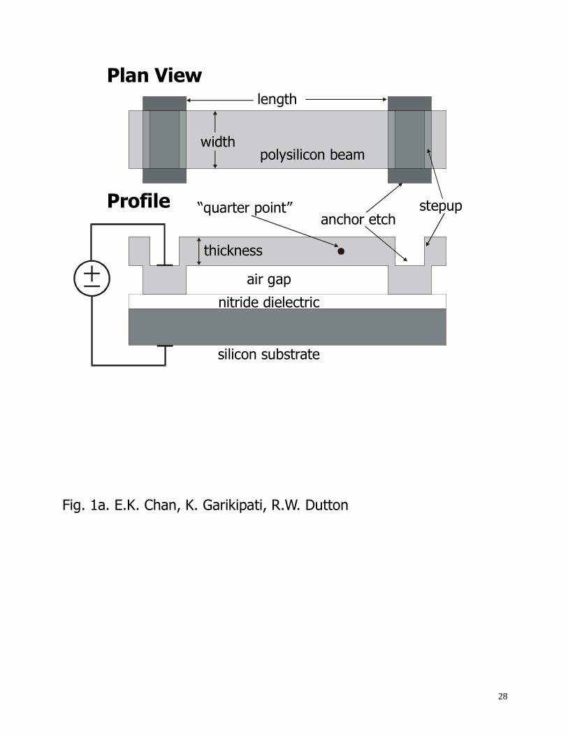
Fig. 1a shows both a plan view and a profile of electrostatically actuated beams fabricated
in the MUMPs process of MCNC. The stepup anchors were designed such that the entire structure
is essentially two-dimensional and beam lengths are well-defined. Standard design rules actually
require that the anchor be surrounded on all sides by polysilicon (Fig. 1b) leading to indistinct
beam lengths and three-dimensional effects due to the enclosure lip.
Applying a voltage between the beam and silicon substrate produces an electric field which
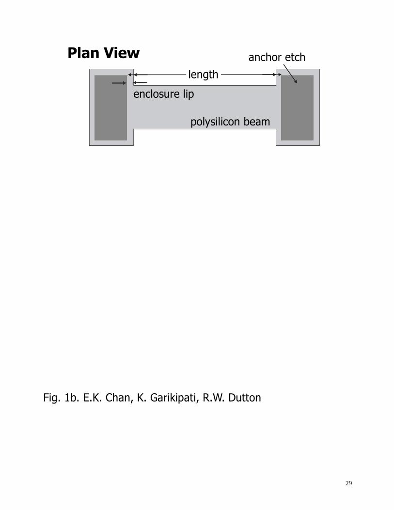
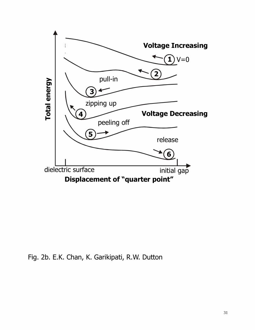
causes the beam to deflect downwards. Fig. 2a shows a typical measurement and simulation of the
capacitance between the beam and silicon substrate as a function of applied voltage with regions
numbered corresponding to those in Fig. 2b. The initial capacitance — the capacitance at no
applied bias voltage — is subtracted from all measured and simulated capacitances. Fig. 2b is a
schematic plot of the total energy of the electromechanical system as a function of the displacement
of the “quarter point” midway between the support post and center of the beam (see Fig. 1a), and
4
parameterized by voltage. The numbered circles indicate the displacement at equilibrium. As the
voltage is increased, the characteristic “pull-in” phenomenon occurs when the barrier between the
two minima in Region 2 disappears at the pull-in voltage (Vpi) and a portion of the beam comes
into contact with the surface of the dielectric. This causes a sharp increase in capacitance. As the
voltage continues to increase, more of the beam contacts the dielectric — the so-called “zip up” —
and the capacitance increases. When the applied voltage is decreased, the quarter-point moves
away from the surface, i.e. the beam “peels off”, but still remains in the same local energy
minimum region. Eventually, the barrier between the minima disappears and the entire beam pops
off the surface of the dielectric causing a sharp decrease in capacitance.
B. Mechanical Model
This electromechanical system is simulated in Abaqus with the electrostatic force applied to
the bottom surface of the beam as a user-defined load [11], [12]. The 2D Abaqus simulation
provides good mechanical accuracy by including the effects of finite deformation (large rotations
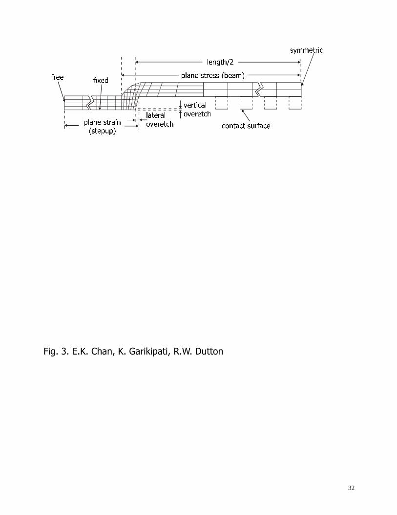
and stress stiffening), compliant stepups and contact. The Abaqus model (Fig. 3) uses 2D reduced-
integration quadratic elements, with plane strain elements for the portion of the stepup anchor
which adheres to the dielectric surface, and plane stress elements for everything else. Interface
elements are used to model the contact surface which is the top of the nitride. The rounded edge of
the top of the stepup due to conformal deposition, the sloping edge of the bottom of the stepup due
to lateral overetch, and the vertical overetching of the nitride under the anchor are modeled [19].
While it is necessary to include the stepups explicitly in the simulation model instead of assuming
perfectly fixed boundaries [20], small variations in the detailed geometry of the stepups have only
minor effects on the simulations with the lateral overetch parameter being the most influential.
5
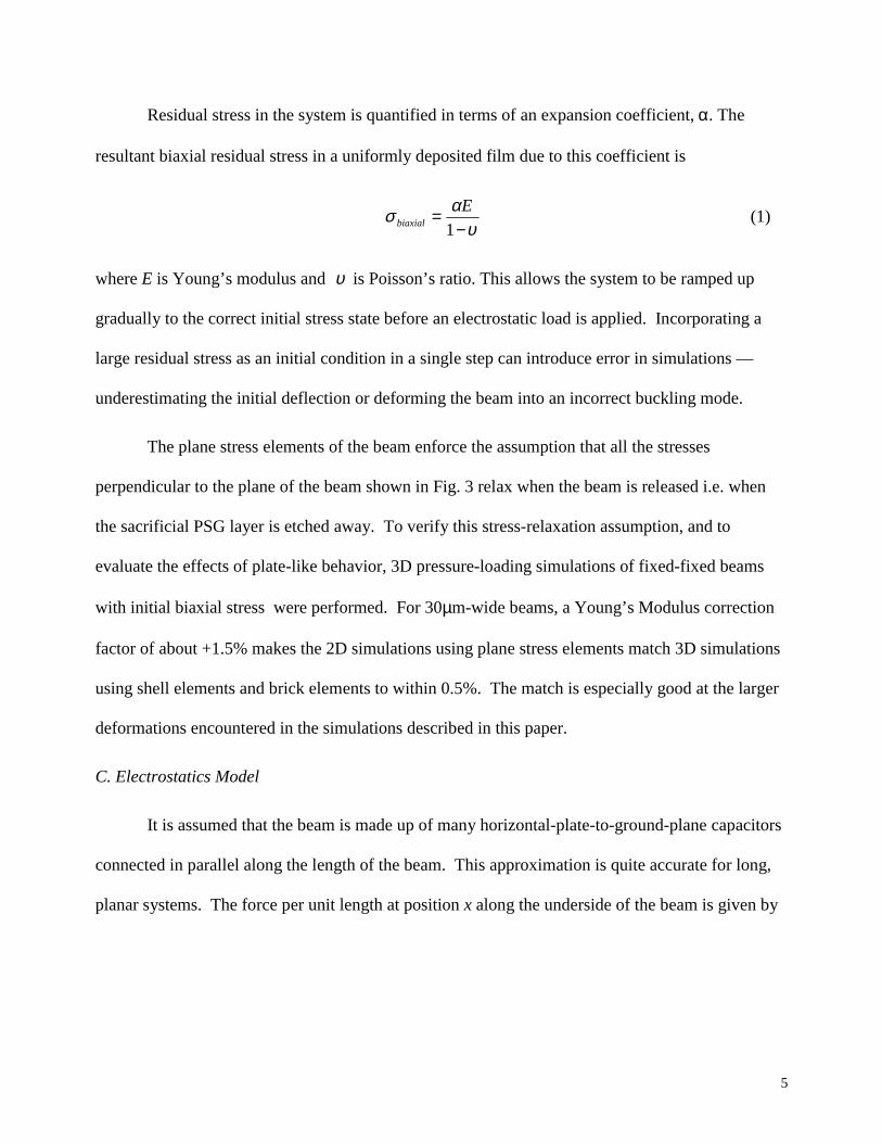
Residual stress in the system is quantified in terms of an expansion coefficient, α. The
resultant biaxial residual stress in a uniformly deposited film due to this coefficient is
υασ−
=1
Ebiaxial (1)
where E is Young’s modulus and υ is Poisson’s ratio. This allows the system to be ramped up
gradually to the correct initial stress state before an electrostatic load is applied. Incorporating a
large residual stress as an initial condition in a single step can introduce error in simulations —
underestimating the initial deflection or deforming the beam into an incorrect buckling mode.
The plane stress elements of the beam enforce the assumption that all the stresses
perpendicular to the plane of the beam shown in Fig. 3 relax when the beam is released i.e. when
the sacrificial PSG layer is etched away. To verify this stress-relaxation assumption, and to
evaluate the effects of plate-like behavior, 3D pressure-loading simulations of fixed-fixed beams
with initial biaxial stress were performed. For 30µm-wide beams, a Young’s Modulus correction
factor of about +1.5% makes the 2D simulations using plane stress elements match 3D simulations
using shell elements and brick elements to within 0.5%. The match is especially good at the larger
deformations encountered in the simulations described in this paper.
C. Electrostatics Model
It is assumed that the beam is made up of many horizontal-plate-to-ground-plane capacitors
connected in parallel along the length of the beam. This approximation is quite accurate for long,
planar systems. The force per unit length at position x along the underside of the beam is given by
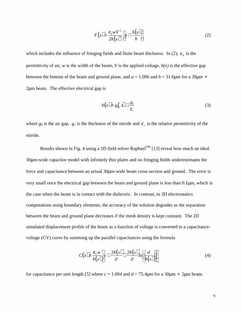
6
( ) ( )( )
+=
b
xha
xh
wVxF 2
20
2
ε(2)
which includes the influence of fringing fields and finite beam thickness. In (2), 0ε is the
permittivity of air, w is the width of the beam, V is the applied voltage, h(x) is the effective gap
between the bottom of the beam and ground plane, and a = 1.006 and b = 31.6µm for a 30µm ×
2µm beam. The effective electrical gap is
( ) ( )r
gxgxh
ε1
0 += (3)
where g0 is the air gap, g1 is the thickness of the nitride and rε is the relative permittivity of the
nitride.
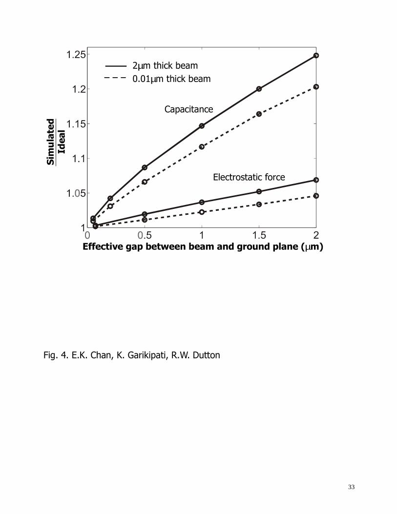
Results shown in Fig. 4 using a 2D field solver RaphaelTM [13] reveal how much an ideal
30µm-wide capacitor model with infinitely thin plates and no fringing fields underestimates the
force and capacitance between an actual 30µm-wide beam cross-section and ground. The error is
very small once the electrical gap between the beam and ground plane is less than 0.1µm, which is
the case when the beam is in contact with the dielectric. In contrast, in 3D electrostatics
computations using boundary elements, the accuracy of the solution degrades as the separation
between the beam and ground plane decreases if the mesh density is kept constant. The 2D
simulated displacement profile of the beam as a function of voltage is converted to a capacitance-
voltage (CV) curve by summing up the parallel capacitances using the formula
( ) ( )( ) ( )
( )
++=xh
d
d
xh
d
xhc
xh
wxC ln
220ε (4)
for capacitance per unit length [5] where c = 1.004 and d = 75.4µm for a 30µm × 2µm beam.
7
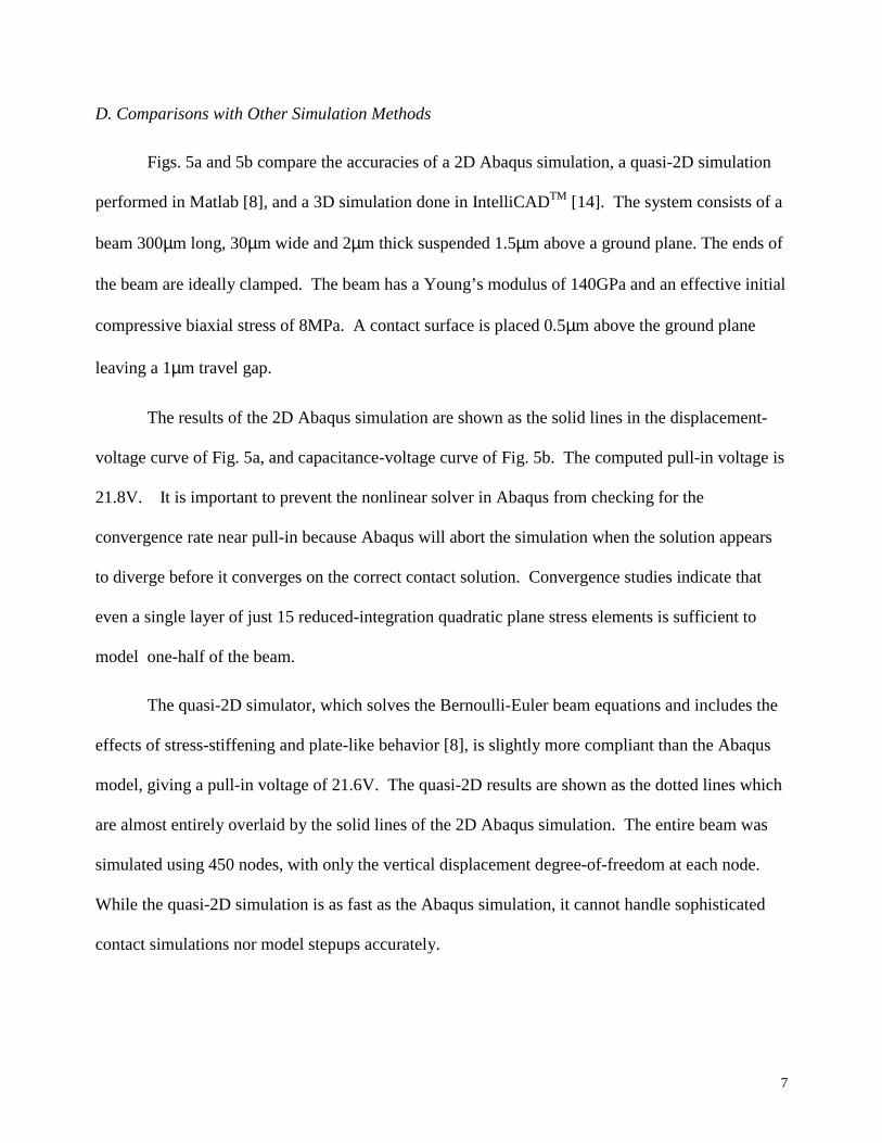
D. Comparisons with Other Simulation Methods
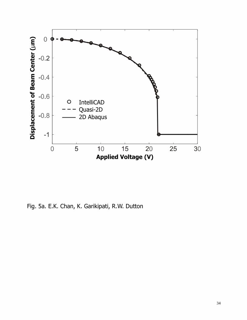
Figs. 5a and 5b compare the accuracies of a 2D Abaqus simulation, a quasi-2D simulation
performed in Matlab [8], and a 3D simulation done in IntelliCADTM [14]. The system consists of a
beam 300µm long, 30µm wide and 2µm thick suspended 1.5µm above a ground plane. The ends of
the beam are ideally clamped. The beam has a Young’s modulus of 140GPa and an effective initial
compressive biaxial stress of 8MPa. A contact surface is placed 0.5µm above the ground plane
leaving a 1µm travel gap.
The results of the 2D Abaqus simulation are shown as the solid lines in the displacement-
voltage curve of Fig. 5a, and capacitance-voltage curve of Fig. 5b. The computed pull-in voltage is
21.8V. It is important to prevent the nonlinear solver in Abaqus from checking for the
convergence rate near pull-in because Abaqus will abort the simulation when the solution appears
to diverge before it converges on the correct contact solution. Convergence studies indicate that
even a single layer of just 15 reduced-integration quadratic plane stress elements is sufficient to
model one-half of the beam.
The quasi-2D simulator, which solves the Bernoulli-Euler beam equations and includes the
effects of stress-stiffening and plate-like behavior [8], is slightly more compliant than the Abaqus
model, giving a pull-in voltage of 21.6V. The quasi-2D results are shown as the dotted lines which
are almost entirely overlaid by the solid lines of the 2D Abaqus simulation. The entire beam was
simulated using 450 nodes, with only the vertical displacement degree-of-freedom at each node.
While the quasi-2D simulation is as fast as the Abaqus simulation, it cannot handle sophisticated
contact simulations nor model stepups accurately.

8
The beam mesh in IntelliCAD consists of 30 × 3 × 1 quadratic brick elements. This model
is slightly stiffer than the Abaqus model, giving a pull-in voltage somewhere between 21.8 and
22V. The longitudinal mesh density for the mechanical model in IntelliCAD is the same as that
used in the Abaqus model. The mesh for electrostatics on the underside of the beam and on the top
of the ground plane are manually refined to obtain the necessary accuracy. The final electrostatics
mesh consists of triangular surfaces with edge lengths of 5µm and 7.5µm on the beam and ground
plane respectively. The IntelliCAD computation consumes well over two orders of magnitude
more time (about 30 minutes per data point on a SUN Ultrasparc 2 with 1GB memory) than the
Abaqus simulation especially near pull-in, with most of the time spent in the electrostatics
solutions. Very little out-of-plane bending is observed, confirming that the problem is essentially
two-dimensional i.e. the beam hardly deforms along the direction of the width of the beam. Hence
electrostatic forces along the width can be lumped together assuming that the beam is rigid in that
direction even though the forces are non-uniform and concentrated near the edges of the beam.
III. G EOMETRICAL MEASUREMENTS
Fixed-fixed beams and cantilevers of various lengths were fabricated in the POLY1
polysilicon layer on the MUMPs 25 run. A Zygo NewView 2000 white-light interferometer was
used to survey the structures and showed that the fixed-fixed beams were flat (less than 0.03µm of
deflection at the center) up until lengths of 520µm. The center deflection of a 600µm beam was
about 0.5µm. A small stress gradient, which does not affect the behavior of fixed-fixed beams
appreciably, caused the cantilevers to curl towards the substrate.
The thickness of the polysilicon was determined from a measurement of a long beam that
buckled downwards and contacted the underlying layer. The air gap was determined by subtracting
that polysilicon thickness from the height of a polysilicon-sacrificial-PSG stack. The electrical
9
thickness of the nitride (thickness divided by rε ) was determined from a capacitance measurement
of a polysilicon layer (POLY0) deposited directly on the nitride. The capacitance did not change as
the DC bias was swept from -35V to 35V, indicating that the polarizability of the nitride dielectric
is independent of the applied electric field, and that carrier depletion in the polysilicon is not
significant. This nitride thickness measurement neglects any overetch due to the etching of
polysilicon and PSG layers [6].
Table 1 contains the parameters that are used in all simulations that follow unless noted
otherwise. Beam widths (all 30µm) and lengths are assumed as drawn since linewidth resolution is
better than 0.1µm [15]. Perfect conformal deposition is assumed, and Poisson’s ratio is taken as
0.23.
IV. ELECTRICAL MEASUREMENTS
A. Pull-in Voltage Measurements
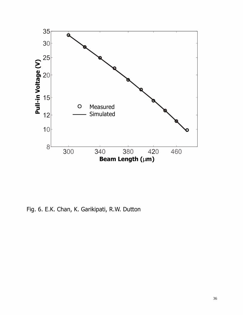
Vpi’s, pull-in voltages at which the capacitances of the systems increase abruptly, were
measured using an HP4275A capacitance meter with DC bias steps of 0.1V and a 100kHz signal of
50mVrms. Both positive and negative biases were applied to account for fixed dielectric charge as
explained further in Section IV.B. The die was in a Gel-PakTM tray. Measured Vpi’s as a function
of beam length are plotted on a log-log scale in Fig. 6. These measurements were confirmed by
using an HP4155A to source a constant 20pA current and observing the voltage of the beam
increase as a function of time. At pull-in, the capacitance increases abruptly and the voltage of the
beam has to decrease momentarily due to charge conservation. The constant-current measurements
confirm that resonance excitation due to the AC signal of the capacitance meter, if occuring at all,
does not affect the measurements, probably because squeezed-film damping is significant.
10
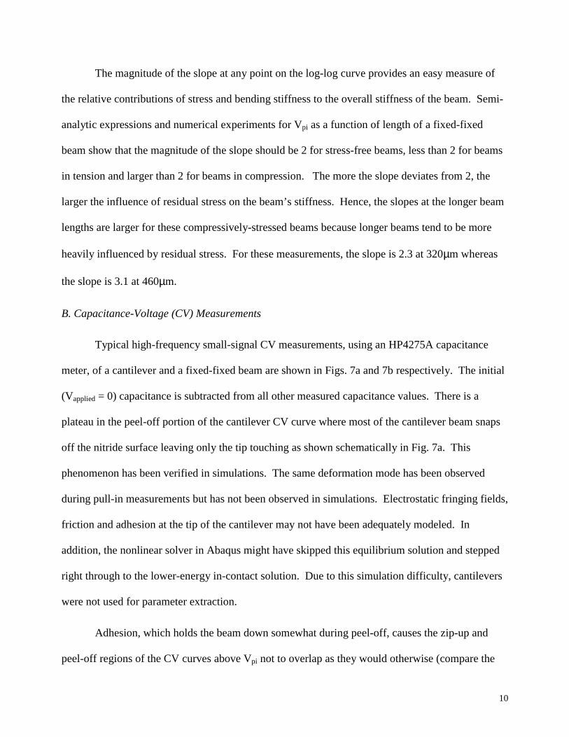
The magnitude of the slope at any point on the log-log curve provides an easy measure of
the relative contributions of stress and bending stiffness to the overall stiffness of the beam. Semi-
analytic expressions and numerical experiments for Vpi as a function of length of a fixed-fixed
beam show that the magnitude of the slope should be 2 for stress-free beams, less than 2 for beams
in tension and larger than 2 for beams in compression. The more the slope deviates from 2, the
larger the influence of residual stress on the beam’s stiffness. Hence, the slopes at the longer beam
lengths are larger for these compressively-stressed beams because longer beams tend to be more
heavily influenced by residual stress. For these measurements, the slope is 2.3 at 320µm whereas
the slope is 3.1 at 460µm.
B. Capacitance-Voltage (CV) Measurements
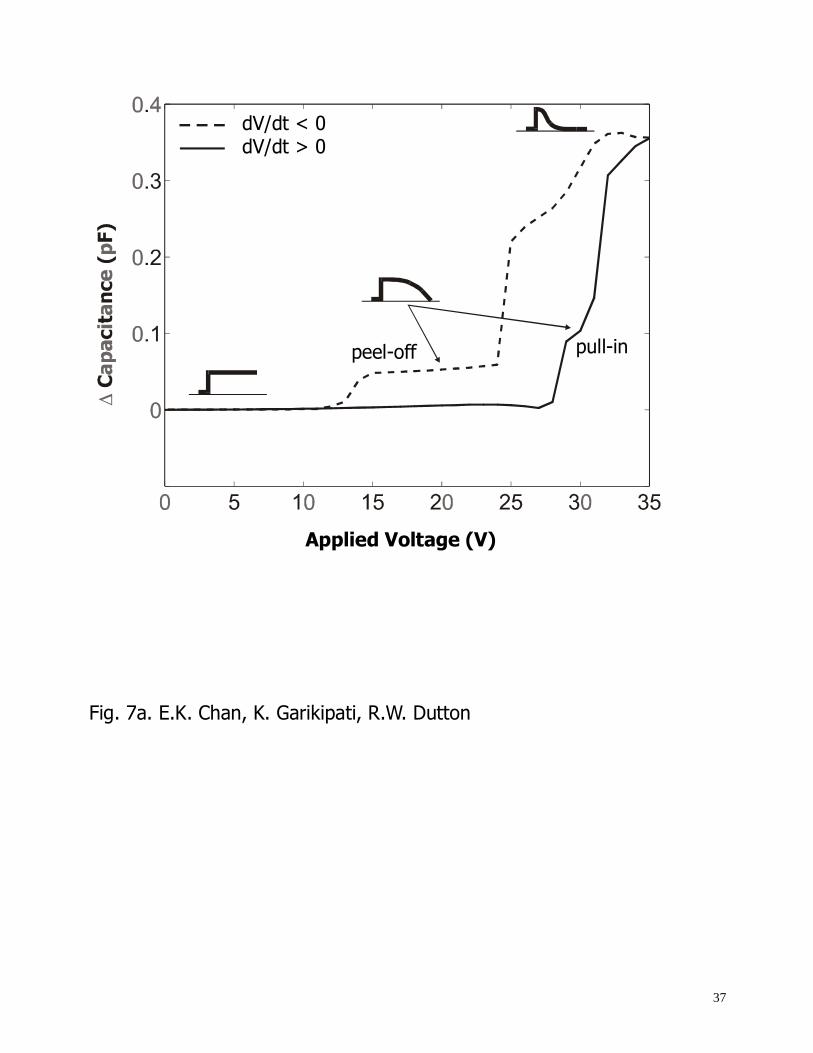
Typical high-frequency small-signal CV measurements, using an HP4275A capacitance
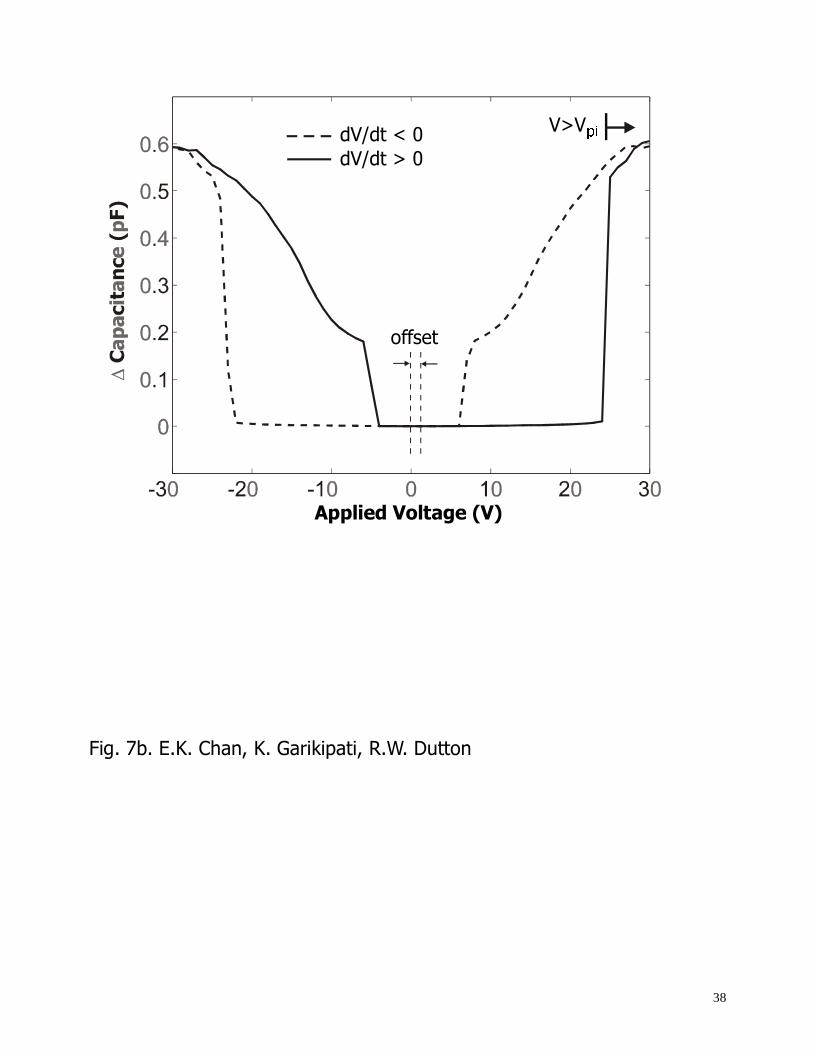
meter, of a cantilever and a fixed-fixed beam are shown in Figs. 7a and 7b respectively. The initial
(Vapplied = 0) capacitance is subtracted from all other measured capacitance values. There is a
plateau in the peel-off portion of the cantilever CV curve where most of the cantilever beam snaps
off the nitride surface leaving only the tip touching as shown schematically in Fig. 7a. This
phenomenon has been verified in simulations. The same deformation mode has been observed
during pull-in measurements but has not been observed in simulations. Electrostatic fringing fields,
friction and adhesion at the tip of the cantilever may not have been adequately modeled. In
addition, the nonlinear solver in Abaqus might have skipped this equilibrium solution and stepped
right through to the lower-energy in-contact solution. Due to this simulation difficulty, cantilevers
were not used for parameter extraction.
Adhesion, which holds the beam down somewhat during peel-off, causes the zip-up and
peel-off regions of the CV curves above Vpi not to overlap as they would otherwise (compare the
11
regions V>Vpi in Figs. 2a and 7b). Trapped charge in the nitride shifts the measured Vpi’s and
offsets the CV measurements along the voltage axis as shown in Fig. 7b. Assuming a sheet of
charge in the nitride, the offset voltage is
r
foffset
zV
εερ
0
= (5)
where fρ is the areal charge density, z is the distance of the charge sheet from the silicon nitride-
silicon substrate interface and rε is the relative permittivity of the nitride. To quantify this charge,
Vpi’s were measured by applying both positive and negative voltages. Theoretically, the positive
and negative Vpi’s should be of the same magnitude since the electrostatic force is proportional to
the square of the applied voltage. The measured differences between the magnitudes were less than
0.2V after allowing more than 5 minutes between measurements. The voltage offsets are one-half
of those differences. Assuming all the charge is on the top surface of the nitride, fρ is less than
1010 e cm-2 where e is the charge of an electron. Thus, fixed charge is not a major problem: all the
Vpi and CV measurements can be adjusted by the measured fixed offset.
Mobile charge, however, seriously distorts the measurements. The magnitudes of Vpi’s
measured in quick succession i.e. less than 1 minute between measurements are progressively
lower. This indicates that charge of polarity opposite to that of the voltage on the beam is being
accumulated in the nitride with each measurement, hence requiring less voltage to pull the beam in.
The further the charge is away from the silicon nitride-silicon substrate interface, the more
influence it has as shown by Eq. 5.
In order to avoid charge buildup, especially at high voltages, and to avoid adhesion effects,
capacitance measurements were made quickly as the beams were zipping up instead of when the

12
beams were peeling off. It is assumed that adhesion is a very short-range force which has no effect
until two surfaces are in contact, and therefore does not influence the zipping-up process where
electrostatic forces dominate. While holding the voltage steady at a value well below pull-in but
still high enough to hold the beam down once the beam is in contact with the nitride surface,
contact is induced by pushing the beam down with a probe tip. The voltage is then ramped up
while capacitance is measured. This measurement takes about 10 seconds; results are shown in
Fig. 10 for several beams.
C. Charge Buildup in Silicon Nitride
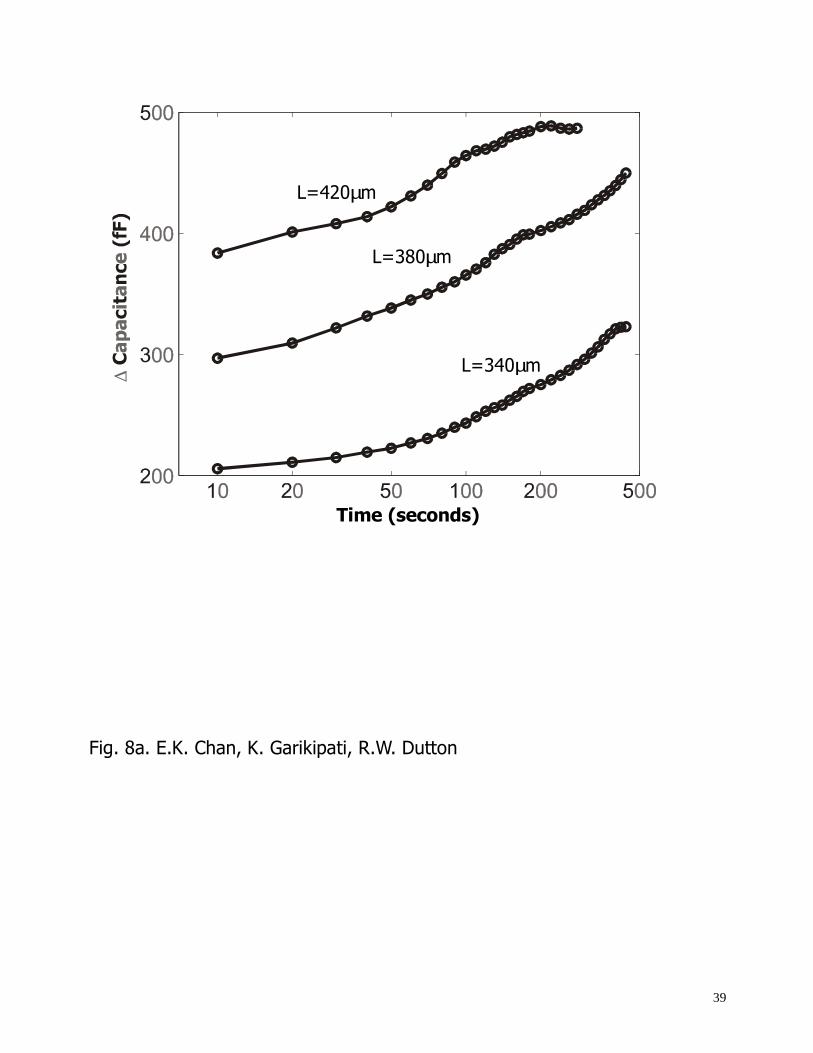
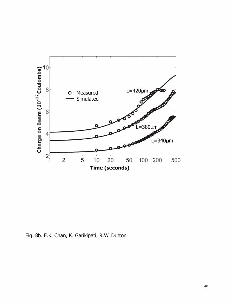
Fig. 8a shows the high-frequency small-signal capacitances of 340µm, 380µm and 420µm
beams in contact with the nitride dielectric measured as functions of time with 12V applied
between the beam and silicon substrate. The measurements shown are those using 100kHz
50mVrms sensing signals but the measurements show no dependence on signal amplitude or
frequency. These measurements indicate that charge builds up over time in the nitride when the
beam is in contact with the nitride surface. The polarity of the charge is opposite to that on the
beam thus attracting more of the beam into contact and increasing the capacitance of the system.
Ordinarily, the charge stored on the plates of a capacitor is determined by both the
capacitance and voltage across that capacitor. For this contact-electromechanical capacitor,
however, the high-frequency small-signal capacitance has a one-to-one correspondence to the
charge on the polysilicon beam which in turn depends on the charge on the silicon substrate surface
and in the nitride dielectric. The shape of the beam, and thus the capacitance of the system,
depends on the charge on the polysilicon beam. Hence, the charge on the polysilicon beam can be
determined from measurements of capacitance alone regardless of the applied voltage. It is
important to note that the polysilicon charge can change even when the applied voltage is held
13
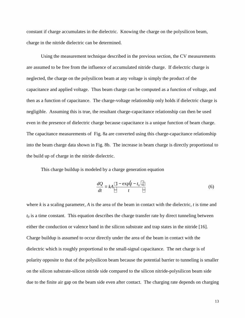
constant if charge accumulates in the dielectric. Knowing the charge on the polysilicon beam,
charge in the nitride dielectric can be determined.
Using the measurement technique described in the previous section, the CV measurements
are assumed to be free from the influence of accumulated nitride charge. If dielectric charge is
neglected, the charge on the polysilicon beam at any voltage is simply the product of the
capacitance and applied voltage. Thus beam charge can be computed as a function of voltage, and
then as a function of capacitance. The charge-voltage relationship only holds if dielectric charge is
negligible. Assuming this is true, the resultant charge-capacitance relationship can then be used
even in the presence of dielectric charge because capacitance is a unique function of beam charge.
The capacitance measurements of Fig. 8a are converted using this charge-capacitance relationship
into the beam charge data shown in Fig. 8b. The increase in beam charge is directly proportional to
the build up of charge in the nitride dielectric.
This charge buildup is modeled by a charge generation equation
( )
−−=
t
ttkA
dt
dQ 0exp1(6)
where k is a scaling parameter, A is the area of the beam in contact with the dielectric, t is time and
t0 is a time constant. This equation describes the charge transfer rate by direct tunneling between
either the conduction or valence band in the silicon substrate and trap states in the nitride [16].
Charge buildup is assumed to occur directly under the area of the beam in contact with the
dielectric which is roughly proportional to the small-signal capacitance. The net charge is of
polarity opposite to that of the polysilicon beam because the potential barrier to tunneling is smaller
on the silicon substrate-silicon nitride side compared to the silicon nitride-polysilicon beam side
due to the finite air gap on the beam side even after contact. The charging rate depends on charging

14
history, remnant charge and applied electric field, and also on material properties such as
stoichiometry and interface conditions. The integration constant resulting from integrating Eq. 6
quantifies the initial charge including the remnant charge in the system due to repeated prolonged
applied electric fields. It cannot be determined from these measurements whether the mobile
species are electrons or holes. Fig. 8c shows similar charge build up for a 340µm beam at three
different constant applied voltages.
V. MATERIAL PROPERTIES EXTRACTION
A. Multiple-device Extraction (from several Vpi’s)
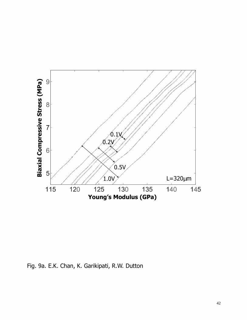
With the geometrical measurements of Table I and Vpi’s, Young’s modulus (E) and biaxial
residual stress (σbiaxial) can be extracted. Fig. 9a shows contours of simulatedpi
measuredpi VV − in E-σbiaxial
space of a 320µm fixed- fixed beam. All simulations using E-σbiaxial pairs within the narrowest
contour (0.1V) give simulated pull-in voltages within 0.1V of the measured value. Similar
contours can be obtained for a beam of a different length (Fig. 9b) and the region where the 0.1V
contours of the two beams overlap is the region in E-σbiaxial space which gives the correct value of
Vpi for both beams. By overlaying the contours for 320µm and 460µm beams, and assuming a
resolution in Vpi of ± 0.1V, we obtain the darker shaded region in Fig. 9b which gives E =
134.8± 2.1GPa and σbiaxial = -7.6± 0.4MPa. The uncertainties in E and σbiaxial increase to 4.8GPa
and 0.8MPa respectively as shown by the lighter shaded region if the Vpi resolution is only ± 0.2V.
The larger the difference in beam lengths, the smaller the uncertainty in extracted parameters. The
extracted E is similar to what was obtained by Sharpe et.al. [21] but lower than that obtained by
Gupta et.al. [6], [17].
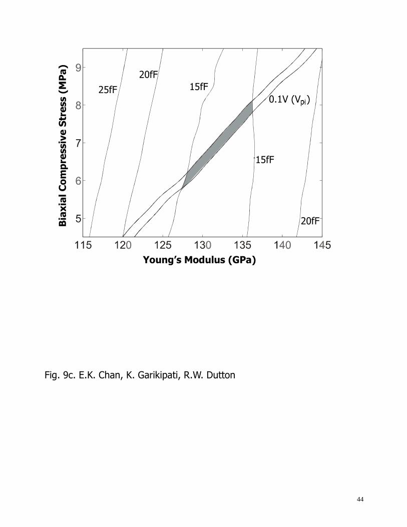
B. Single-device Extraction (from Vpi and CV curve)
15
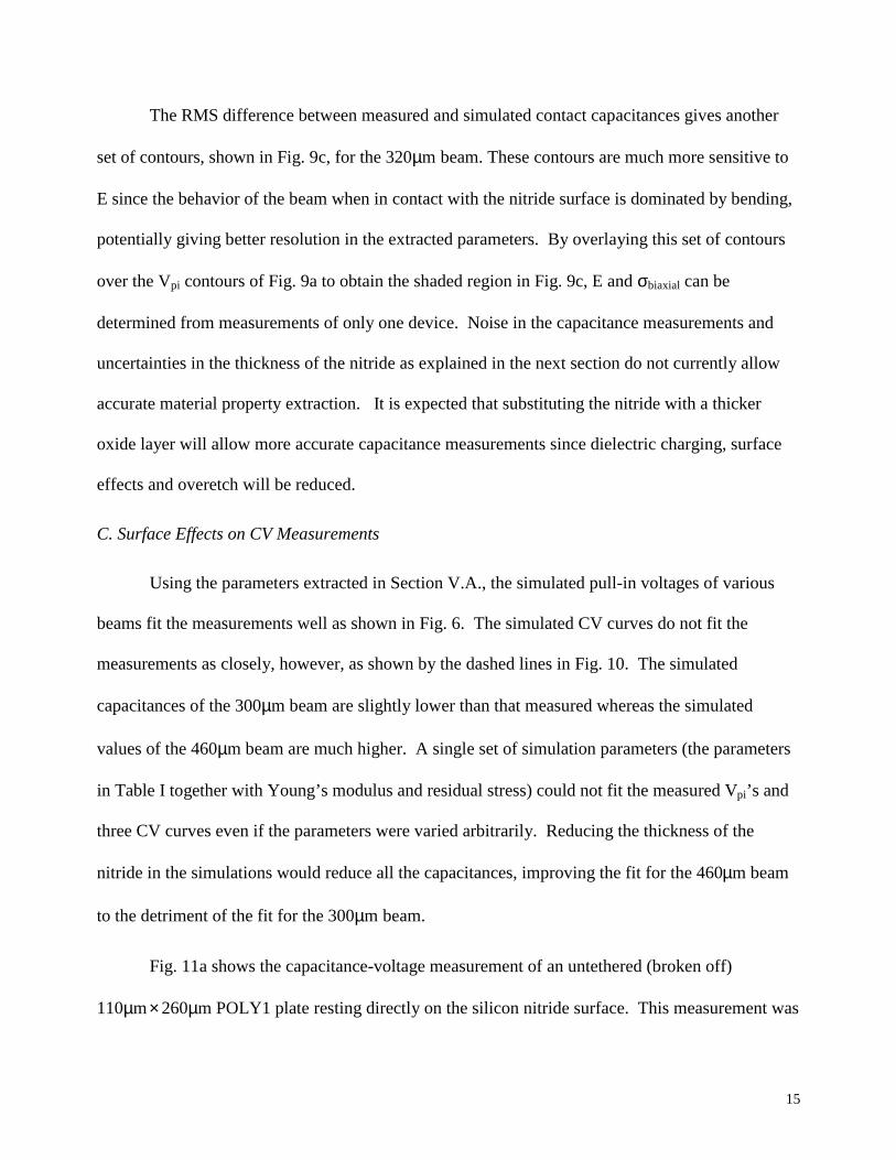
The RMS difference between measured and simulated contact capacitances gives another
set of contours, shown in Fig. 9c, for the 320µm beam. These contours are much more sensitive to
E since the behavior of the beam when in contact with the nitride surface is dominated by bending,
potentially giving better resolution in the extracted parameters. By overlaying this set of contours
over the Vpi contours of Fig. 9a to obtain the shaded region in Fig. 9c, E and σbiaxial can be
determined from measurements of only one device. Noise in the capacitance measurements and
uncertainties in the thickness of the nitride as explained in the next section do not currently allow
accurate material property extraction. It is expected that substituting the nitride with a thicker
oxide layer will allow more accurate capacitance measurements since dielectric charging, surface
effects and overetch will be reduced.
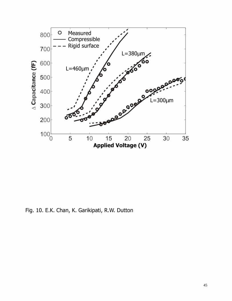
C. Surface Effects on CV Measurements
Using the parameters extracted in Section V.A., the simulated pull-in voltages of various
beams fit the measurements well as shown in Fig. 6. The simulated CV curves do not fit the
measurements as closely, however, as shown by the dashed lines in Fig. 10. The simulated
capacitances of the 300µm beam are slightly lower than that measured whereas the simulated
values of the 460µm beam are much higher. A single set of simulation parameters (the parameters
in Table I together with Young’s modulus and residual stress) could not fit the measured Vpi’s and
three CV curves even if the parameters were varied arbitrarily. Reducing the thickness of the
nitride in the simulations would reduce all the capacitances, improving the fit for the 460µm beam
to the detriment of the fit for the 300µm beam.
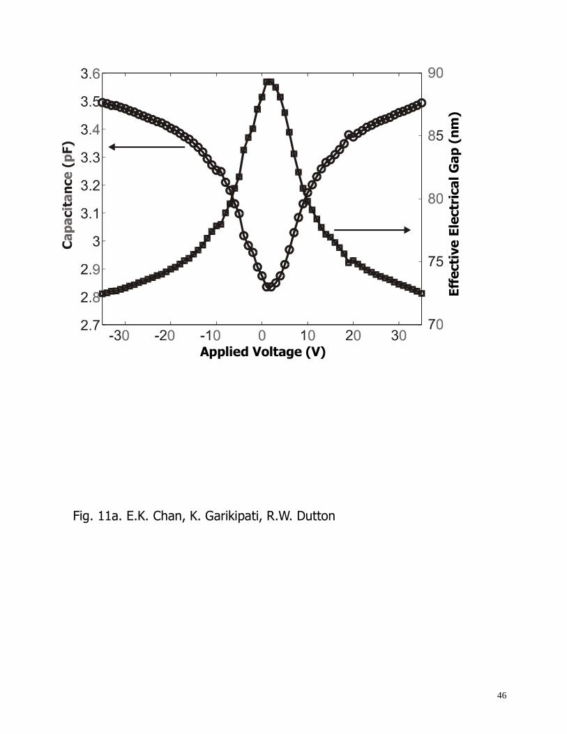
Fig. 11a shows the capacitance-voltage measurement of an untethered (broken off)
110µm× 260µm POLY1 plate resting directly on the silicon nitride surface. This measurement was
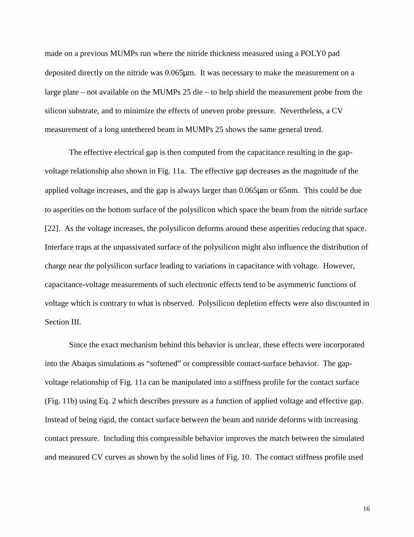
16
made on a previous MUMPs run where the nitride thickness measured using a POLY0 pad
deposited directly on the nitride was 0.065µm. It was necessary to make the measurement on a
large plate – not available on the MUMPs 25 die – to help shield the measurement probe from the
silicon substrate, and to minimize the effects of uneven probe pressure. Nevertheless, a CV
measurement of a long untethered beam in MUMPs 25 shows the same general trend.
The effective electrical gap is then computed from the capacitance resulting in the gap-
voltage relationship also shown in Fig. 11a. The effective gap decreases as the magnitude of the
applied voltage increases, and the gap is always larger than 0.065µm or 65nm. This could be due
to asperities on the bottom surface of the polysilicon which space the beam from the nitride surface
[22]. As the voltage increases, the polysilicon deforms around these asperities reducing that space.
Interface traps at the unpassivated surface of the polysilicon might also influence the distribution of
charge near the polysilicon surface leading to variations in capacitance with voltage. However,
capacitance-voltage measurements of such electronic effects tend to be asymmetric functions of
voltage which is contrary to what is observed. Polysilicon depletion effects were also discounted in
Section III.
Since the exact mechanism behind this behavior is unclear, these effects were incorporated
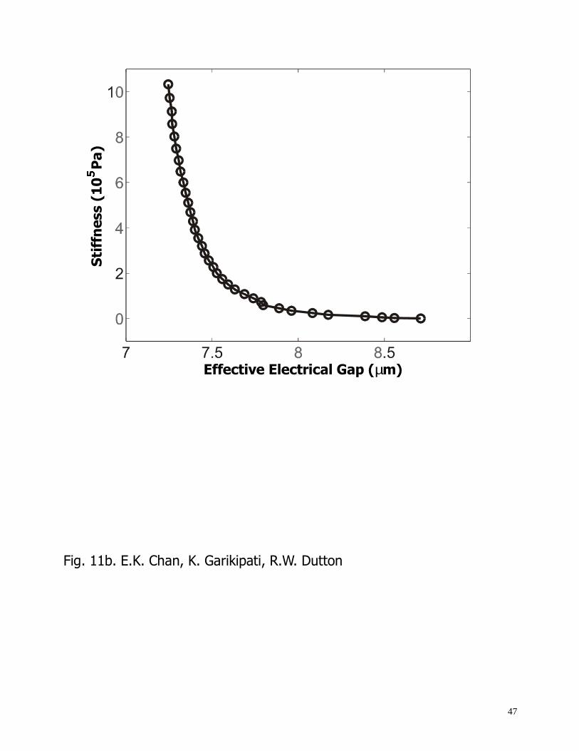
into the Abaqus simulations as “softened” or compressible contact-surface behavior. The gap-
voltage relationship of Fig. 11a can be manipulated into a stiffness profile for the contact surface
(Fig. 11b) using Eq. 2 which describes pressure as a function of applied voltage and effective gap.
Instead of being rigid, the contact surface between the beam and nitride deforms with increasing
contact pressure. Including this compressible behavior improves the match between the simulated
and measured CV curves as shown by the solid lines of Fig. 10. The contact stiffness profile used
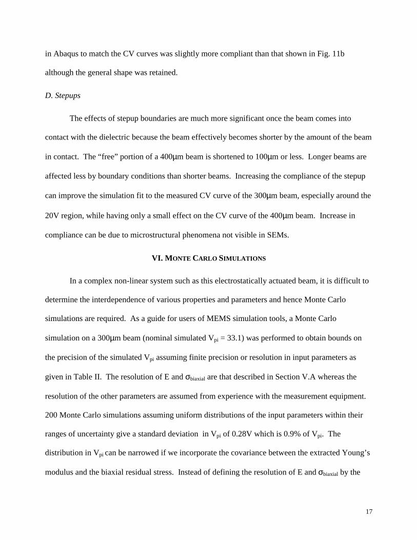
17
in Abaqus to match the CV curves was slightly more compliant than that shown in Fig. 11b
although the general shape was retained.
D. Stepups
The effects of stepup boundaries are much more significant once the beam comes into
contact with the dielectric because the beam effectively becomes shorter by the amount of the beam
in contact. The “free” portion of a 400µm beam is shortened to 100µm or less. Longer beams are
affected less by boundary conditions than shorter beams. Increasing the compliance of the stepup
can improve the simulation fit to the measured CV curve of the 300µm beam, especially around the
20V region, while having only a small effect on the CV curve of the 400µm beam. Increase in
compliance can be due to microstructural phenomena not visible in SEMs.
VI. M ONTE CARLO SIMULATIONS
In a complex non-linear system such as this electrostatically actuated beam, it is difficult to
determine the interdependence of various properties and parameters and hence Monte Carlo
simulations are required. As a guide for users of MEMS simulation tools, a Monte Carlo
simulation on a 300µm beam (nominal simulated Vpi = 33.1) was performed to obtain bounds on
the precision of the simulated Vpi assuming finite precision or resolution in input parameters as
given in Table II. The resolution of E and σbiaxial are that described in Section V.A whereas the
resolution of the other parameters are assumed from experience with the measurement equipment.
200 Monte Carlo simulations assuming uniform distributions of the input parameters within their
ranges of uncertainty give a standard deviation in Vpi of 0.28V which is 0.9% of Vpi. The
distribution in Vpi can be narrowed if we incorporate the covariance between the extracted Young’s
modulus and the biaxial residual stress. Instead of defining the resolution of E and σbiaxial by the
18
smallest bounding rectangle of the overlap space in Fig. 9b, we can define the the extracted E and
σbiaxial to be exactly the parallelogram of the overlap. This covariance information, however, is not
easily incorporated into most simulation systems.
VII. C ONCLUSION
The behavior of electrostatically actuated polysilicon beams, with an emphasis on the
behavior when the beam is in contact with an underlying silicon nitride dielectric layer, has been
described through capacitance-voltage measurements and simulations. A method to extract both E
and σbiaxial from measurements of a single device has been presented although the resolution of the
method is impaired by dielectric charging, surface effects and overetch. Charge buildup over time
in the electromechanical system at constant applied voltages was measured and modeled as charge
trapping via direct tunneling into the nitride. Capacitance-voltage measurements of several devices
reveal that surface effects, which can be captured by a compressible-contact-surface model,
strongly influence the contact electromechanics of this system. All these effects must be
considered to effectively design devices operating in contact such as capacitive microwave
switches.
ACKNOWLEDGEMENTS
The authors would like to thank E. C. Kan of Cornell University, D. W. Burns of Maxim, and C. R.
Steele and B. R. Fulton of Stanford University for their time and valuable comments. This work
was supported by the DARPA Composite CAD program (F30602-96-2-0308-P00001).
REFERENCES
[1] C. Goldsmith, J. Randall, S. Eshelman, T. H. Lin, D. Denniston, S. Chen, B. Norvell,
“Characteristics of micromachined switches at microwave frequencies,” in IEEE MTT-S
19
International Microwave Symposium Digest, vol. 2, San Francisco, pp. 1141-1144, June
1996.
[2] J. D. Zook, D. W. Burns, H. Guckel, J. J. Sniegowski, R. L. Engelstad, Z. Feng,
“Characteristics of polysilicon resonant microbeams,” Sensors and Actuators A, vol A35,
no. 1, pp. 51-59, October 1992.
[3] C. T. -C. Nguyen, “Micromechanical resonators for oscillators and filters,” in Proceedings
of IEEE Ultrasonics Symposium, vol. 1, Seattle, pp. 489-499, November 1995.
[4] K. Najafi, K. Suzuki, “Measurement of fracture stress, Young’s modulus, and intrinsic
stress of heavily boron-doped silicon microstructures,” Thin Solid Films, vol. 181, pp. 251-
258, December 1989.
[5] P. M. Osterberg, S. D. Senturia, “M-TEST: A test chip for MEMS material property
measurement using electrostatically actuated test structures,” Journal of
Microelectromechanical Systems, vol. 6, no. 2, pp. 107-118, June 1997.
[6] R. K. Gupta, “Electrostatic pull-in test structure design for in-situ mechanical property
measurements of microelectromechanical systems (MEMS),” Ph.D. Thesis, Massachusetts
Institute of Technology, USA, June 1997.
[7] H. C. Nathanson, W. E. Newell, R. A. Wickstrom, J. R. Davis, Jr., “The resonant gate
transistor,” IEEE Transactions on Electron Devices, vol. ED-14, no. 3, pp. 117-125, March
1967.
[8] E. K. Chan, E. C. Kan, P. M. Pinsky, R. W. Dutton, “Nonlinear dynamic modeling of
micromachined microwave switches,” in IEEE MTT-S International Microwave Symposium
Digest, vol. 3, Denver, pp. 1511-1514, June 1997.
20
[9] J. R. Gilbert, G. K. Ananthasuresh, S. D. Senturia, “3D modeling of contact problems and
hysteresis in coupled electro-mechanics,” in Proceedings of Ninth International Workshop
on Microelectromechanical Systems, San Diego, pp. 127-132, February 1996.
[10] Microelectronics Center of North Carolina (MCNC), http://mems.mcnc.org.
[11] Hibbitt, Karlsson and Sorensen, Inc., ABAQUS/Standard User’s Manual, version 5.6,
Pawtucket, 1996.
[12] B. E. Artz, L. W. Cathey, “A finite element method for determining structural
displacements resulting from electrostatic forces,” in Proceedings of IEEE Solid State
Sensor and Actuator Workshop, Hilton Head, pp. 190-193, June 1992.
[13] Technology Modeling Associates, Raphael User’s Manual, version 4.1, Palo Alto, 1997.
[14] IntelliSense Corp., IntelliCAD User’s Manual, version 3.5, Wilmington, 1998.
[15] D. A. Koester, Microelectronics Center of North Carolina, private communication.
[16] D. A. Buchanan, R. A. Abram, M. J. Morant, “Charge trapping in silicon-rich Si3N4 thin
films,” Solid State Electronics, vol. 30, no. 12, pp. 1295-1301, December 1987.
[17] R. K. Gupta, P. M. Osterberg, S. D. Senturia, “Material property measurements of
micromechanical polysilicon beams,” in Proceedings of SPIE 1996 Conference:
Microlithography and metrology in micromachining II, Austin, pp. 39-45, October 1996.
[18] S. Wang, S. Crary, K. Najafi, “Electronic determination of the modulus of elasticity and
intrinsic stress of thin films using capacitive bridges,” in Proceedings of Materials Research
Society Symposium, vol. 276, pp. 203-208, April 1992.
21
[19] J. J. -Y. Gill, L. V. Ngo, P. R. Nelson, C. -J. Kim, “Elimination of extra spring effect at the
step-up anchor of surface-micromachined structure,” Journal of Microelectromechanical
Systems, vol. 7, no. 1, pp. 114-121, March 1998
[20] Q. Meng, M. Mehregany, R. L. Mullen, “Theoretical modeling of microfabricated beams
with elastically restrained supports,” Journal of Microelectromechanical Systems, vol. 2,
no. 3, pp. 128-137, September 1993.
[21] W. N. Sharpe, Jr., K. Turner, R. L. Edwards, “Measurements of the effect of specimen size
on Young's modulus and tensile strength of polysilicon,” in Late News Poster Session
Supplemental Digest of IEEE Solid State Sensor and Actuator Workshop, Hilton Head, pp.
17-18, June 1998.
[22] M. P. de Boer, M. R. Tabbara, M. T. Dugger, P. J. Clews, T. A. Michalske, “Measuring and
modeling electrostatic adhesion in micromachines,” in Proceedings of Transducers ’97,
Chicago, pp. 229-232, June 1997.
22
Biographies
Edward K. Chan grew up in Kuantan, Malaysia before coming to Stanford University where he
received the B.S. and M.S. degrees in Electrical Engineering in 1994 and 1996 respectively. He is
currently working towards a Ph.D. developing computer-aided design (CAD) tools for
microelectromechanical devices.
Krishna Garikipati graduated with a B.Tech. in Aeronautical Engineering from IIT Bombay,
Bombay, India in 1991. At Stanford University, he completed an M.S. in 1992 and a Ph.D. in 1996
in Aeronautics and Astronautics. Currently, he is a Research Associate at the Center for Integrated
Systems.
His research interests lie in the areas of computational nonlinear solid mechanics, theory of
discretization, multiscale modeling, and the application of continuum mechanics and numerical
methods to problems of interest in semiconductor technology.
Robert W. Dutton is Professor of Electrical Engineering at Stanford University and Director of
Research at the Center for Integrated Systems. He received the B.S., M.S., and Ph.D. degrees from
the University of California, Berkeley, in 1966, 1967, and 1970, respectively.
He has held Summer staff positions at Fairchild, Bell Telephone Laboratories, Hewlett-
Packard, IBM Research, and Matsushita in 1967, 1973, 1975, 1977, and 1988 respectively. His
research interests focus on integrated circuit process, device, and circuit technologies -- especially
the use of computer-aided design (CAD) tools and computational methods.

23
Dr. Dutton has published more than 200 journal articles and graduated more than four
dozen doctorate students. He was Editor of the IEEE CAD Journal (1984-1986), winner of the
1987 IEEE J. J. Ebers Award, 1988 Guggenheim Fellowship to study in Japan, was elected to the
National Academy of Engineering in 1991, and winner of the Jack A. Morton Award for 1996.
24
List of tables
Table I. Measured geometrical parameters used in Abaqus simulations.
Table II. Precision or resolution of parameters used in Abaqus simulations.
List of figures
Fig. 1 (a) Plan view and profile of electrostatically actuated beam used in this study, fabricated
in the MUMPs process of MCNC.
(b) Plan view of standard electrostatically actuated beam in compliance with MUMPs
design rules. The anchor etch is completely enclosed by polysilicon creating enclosure
lips that result in indistinct beam lengths and three-dimensional behavior.
Fig. 2 (a) Typical simulated and measured capacitance-voltage (CV) curves of a beam. Initial
capacitances (capacitances at zero applied voltage) are subtracted from subsequent
capacitance values. Regions are numbered corresponding to the curves in Fig. 2b.
(b) Schematic plot of the total energy of an electromechanical system as a function of
the displacement of the “quarter point” on the beam, parameterized by applied voltage.
The regions are numbered corresponding to Fig. 2a and show the equilibrium locations
of the quarter point at pull-in, zip-up, peel-off and release.
Fig. 3 Mesh of 2D Abaqus model. Quadratic reduced-integration elements are used
throughout. Plane strain elements are used to model the stepup which is anchored to the
nitride. Plane stress elements, which enforce the assumption that out-of-plane stress is

25
zero, are used to model the beam. Electrostatic forces are applied to the underside of the
beam.
Fig. 4 Normalized 2D capacitance and electrostatic force of a 30µm-wide beam cross-section
showing the effects of fringing fields and finite beam thickness. Simulations were
performed in RaphaelTM. Ideal analytic calculations neglect fringing fields and assume
infinitely thin electrodes.
Fig. 5 (a) Comparison of displacement-voltage curves of a fixed-fixed beam generated by
quasi-2D (Matlab), 2D (Abaqus) and 3D (IntelliCAD) simulators. The quasi-2D curve,
almost entirely overlaid by the 2D curve, stops just before contact occurs.
(b) Comparison of CV curves corresponding to the displacement-voltage curves of Fig.
5a generated by quasi-2D, 2D and 3D simulators. The effects of fringing fields and
finite beam thickness are included.
Fig. 6 Log-log plot of measured and simulated pull-in voltages (Vpi’s) of fixed-fixed beams as
a function of beam length. The magnitude of the slope at any point indicates the
influence of residual stress on the overall stiffness of the beam – the larger the deviation
from 2, the stronger the influence of residual stress.
Fig. 7 (a) Typical measured capacitance-voltage curve of a cantilever. The plateau in the peel-
off region is where only the tip of the cantilever touches the nitride surface. A similar
deformation mode is observed at pull-in, but only for a small range of voltages.
(b) Typical measured capacitance-voltage curve of a fixed-fixed beam. The CV curve is
offset from the zero-voltage axis-of-symmetry due to dielectric charge. In the region

26
beyond pull-in (V > Vpi), the measured curves do not overlap because adhesion forces
become important during peel-off.
Fig. 8 (a) Measured capacitances of three beams as a function of time at a constant applied
voltage of 12V. Beams are in contact with nitride surface. Initial capacitances
(capacitances at zero applied voltage) are subtracted from all measurements.
(b) Measured and simulated charge on three polysilicon beams as a function of time at a
constant applied voltage of 12V. The measured charge was computed from the
capacitance measurements of Fig. 8a. Eq. 6 describing charge generation was integrated
numerically to obtain the simulated curves. The constants of integration describe the
remnant charge in the system at Time = 0.
(c) Measured and simulated charge on a 340µm polysilicon beam as a function of time
at three constant applied voltages. The rate of charge buildup depends on applied
electric field and charging history.
Fig. 9 (a) Contours of difference between measured and simulated Vpi’s of a 320µm beam in
Young’s modulus (E) – biaxial compressive stress (σb) space. All simulations using E-
σb pairs within the 0.1V contour give pull-in voltages within 0.1V of the measured
value.
(b) Contours of difference between measured and simulated Vpi’s of a 460µm beam.
The lighter and darker shaded areas are the regions in E-σb space that produce simulated
Vpi’s within 0.2 and 0.1 V of the measured values respectively for both the 320µm and
460µm beams.
27
(c) Contours of RMS difference between measured and simulated contact capacitances
of a 320µm beam. The shaded region is the overlap between the 15fF RMS capacitance
contour and the 0.1V Vpi contour indicating the region in E-σb space that matches both
the measured pull-in voltage and CV characteristic.
Fig. 10 Measured and simulated contact CV curves for three beams. The dashed lines are the
simulation results assuming that the contact surface between the polysilicon beam and
nitride is rigid. The solid lines are the simulation results assuming that the contact
surface deforms with increasing applied voltage.
Fig. 11 (a) Total capacitance of a 110µm× 260µm untethered (broken off) polysilicon plate as a
function of voltage. The effective electrical gap was then computed from the
capacitance. The gap decreases with the increasing magnitude of the applied voltage.
The curves are symmetric about a small offset voltage.
(b) Mechanical stiffness of the contact surface as a function of effective electrical gap,
computed from Fig. 11a.
28
3ODQ�9LHZ
ZLGWKSRO\VLOLFRQ�EHDP
OHQJWK
DQFKRU�HWFKVWHSXS³TXDUWHU�SRLQW´3URILOH
DLU�JDS
QLWULGH�GLHOHFWULF
VLOLFRQ�VXEVWUDWH
WKLFNQHVV
)LJ���D��(�.��&KDQ��.��*DULNLSDWL��5�:��'XWWRQ
29
3ODQ�9LHZ
SRO\VLOLFRQ�EHDP
OHQJWK
DQFKRU�HWFK
HQFORVXUH�OLS
)LJ���E��(�.��&KDQ��.��*DULNLSDWL��5�:��'XWWRQ
30
$SSOLHG�9ROWDJH��9�
9!9
0HDVXUHG6LPXODWHG
PHDVXUHPHQW
GLUHFWLRQ�
�
� �
�
�
�
SL
)LJ���D��(�.��&KDQ��.��*DULNLSDWL��5�:��'XWWRQ
31
7RWD
O�HQHUJ
\
'LVSODFHPHQW�RI�³TXDUWHU�SRLQW´
GLHOHFWULF�VXUIDFH LQLWLDO�JDS
9ROWDJH�,QFUHDVLQJ
SXOO�LQ
]LSSLQJ�XS
9ROWDJH�'HFUHDVLQJ
SHHOLQJ�RII
UHOHDVH
�
�
�
�
�
�
9 �
)LJ���E��(�.��&KDQ��.��*DULNLSDWL��5�:��'XWWRQ
32
OHQJWK��
IL[HG
V\PPHWULF
IUHH
SODQH VWUDLQ�VWHSXS�
SODQH VWUHVV �EHDP�
FRQWDFW VXUIDFH
ODWHUDO
RYHUHWFK
YHUWLFDO
RYHUHWFK
)LJ�����(�.��&KDQ��.��*DULNLSDWL��5�:��'XWWRQ
33
6LP
XODWH
G,G
HDO
(IIHFWLYH�JDS�EHWZHHQ�EHDP�DQG�JURXQG�SODQH�� P�µ
� P�WKLFN�EHDPµ���� P�WKLFN�EHDPµ
&DSDFLWDQFH
(OHFWURVWDWLF�IRUFH
)LJ�����(�.��&KDQ��.��*DULNLSDWL��5�:��'XWWRQ
34
'LVSODFHPHQW�RI�%HDP�&HQWH
U��µ
P�
$SSOLHG�9ROWDJH��9�
�'�$EDTXV
,QWHOOL&$'
4XDVL��'
)LJ���D��(�.��&KDQ��.��*DULNLSDWL��5�:��'XWWRQ

35
$SSOLHG�9ROWDJH��9�
�'�$EDTXV
,QWHOOL&$'
4XDVL��'
)LJ���E��(�.��&KDQ��.��*DULNLSDWL��5�:��'XWWRQ
36
%HDP�/HQJWK�� �µP
3XOO�LQ�9ROWDJH��9�
6LPXODWHG0HDVXUHG
)LJ�����(�.��&KDQ��.��*DULNLSDWL��5�:��'XWWRQ
37
$SSOLHG�9ROWDJH��9�
G9�GW����G9�GW�!��
SHHO�RII SXOO�LQ
)LJ���D��(�.��&KDQ��.��*DULNLSDWL��5�:��'XWWRQ
38
$SSOLHG�9ROWDJH��9�
G9�GW����
G9�GW�!��
9!9
RIIVHW
SL
)LJ���E��(�.��&KDQ��.��*DULNLSDWL��5�:��'XWWRQ
39
7LPH��VHFRQGV�
/ ��� Pµ
/ ��� Pµ
/ ��� Pµ
)LJ���D��(�.��&KDQ��.��*DULNLSDWL��5�:��'XWWRQ
40
7LPH��VHFRQGV�
���
/ ��� Pµ
/ ��� Pµ
/ ��� Pµ
0HDVXUHG6LPXODWHG
)LJ���E��(�.��&KDQ��.��*DULNLSDWL��5�:��'XWWRQ

41
7LPH��VHFRQGV�
���
9 ��
9 ��
9 ��
0HDVXUHG6LPXODWHG
)LJ���F��(�.��&KDQ��.��*DULNLSDWL��5�:��'XWWRQ
42
<RXQJ¶V�0RGXOXV��*3D�
%LD[LDO�&RPSUH
VVLYH�6WUHVV��03D�
���9
���9
���9
���9 / ��� Pµ
)LJ���D��(�.��&KDQ��.��*DULNLSDWL��5�:��'XWWRQ

43
<RXQJ¶V�0RGXOXV��*3D�
%LD[LDO�&RPSUH
VVLYH�6WUHVV��03D�
���9
���9
���9
���9 / ��� Pµ
)LJ���E��(�.��&KDQ��.��*DULNLSDWL��5�:��'XWWRQ
44
<RXQJ¶V�0RGXOXV��*3D�
%LD[LDO�&RPSUH
VVLYH�6WUHVV��03D�
���9��9���
��I)
��I)
��I)
��I)
��I)SL
)LJ���F��(�.��&KDQ��.��*DULNLSDWL��5�:��'XWWRQ
45
$SSOLHG�9ROWDJH��9�
5LJLG�VXUIDFH&RPSUHVVLEOH0HDVXUHG
/ ��� Pµ
/ ��� Pµ
/ ��� Pµ
)LJ������(�.��&KDQ��.��*DULNLSDWL��5�:��'XWWRQ
46
$SSOLHG�9ROWDJH��9�
(IIHFWLYH�(OHFWULFDO�*DS��QP�
)LJ����D��(�.��&KDQ��.��*DULNLSDWL��5�:��'XWWRQ
47
(IIHFWLYH�(OHFWULFDO�*DS��µP�
6WLIIQHVV������3D�
�
)LJ����E��(�.��&KDQ��.��*DULNLSDWL��5�:��'XWWRQ
Recommended