CdSe AND ITS HYBRID MATERIALS
FOR
ENERGY APPLICATIONS
A THESIS
SUBMITTED TO THE
UNIVERSITY OF PUNE
FOR THE DEGREE OF
DOCTOR OF PHILOSOPHY
IN
CHEMISTRY
BY
JOYASHISH DEBGUPTA
UNDER THE GUIDANCE OF
Dr. K. VIJAYAMOHANAN
PHYSICAL AND MATERIALS CHEMISTRY DIVISION
NATIONAL CHEMICAL LABORATORY
PUNE-411008
INDIA
JUNE 2014

Dedicated to My Beloved
Late Kakumoni, Phoolpisimoni and Baba

DECLARATION
I, hereby declare that all the experiments embodied in this thesis entitled,
“CdSe AND ITS HYBRID MATERIALS FOR ENERGY APPLICATIONS”,
submitted for the degree of Doctor of Philosophy in Chemistry, to the University
of Pune have been carried out by me at the Physical and Materials Chemistry
Division, National Chemical Laboratory, Pune-411008, India, under the
supervision of Dr. K. Vijayamohanan. The work is original and has not been
submitted in part or full by me, for any degree or diploma to this or to any other
University.
Date: Physical and Materials Chemistry Division National Chemical laboratory Pune-411008
Joyashish Debgupta

CERTIFICATE
This is to certify that the work incorporated in the thesis entitled, “CdSe AND ITS
HYBRID MATERIALS FOR ENERGY APPLICATIONS” submitted by Mr.
JOYASHISH DEBGUPTA, has been carried out by him under my supervision at
the Physical and Materials Chemistry Division, National Chemical Laboratory,
Pune-411008, India. All the materials from other sources have been duly
acknowledged in the thesis.
Date:
Place: Pune
Dr. K. Vijayamohanan
(Research Guide)

Acknowledgements
The PhD research period sustained the most difficult part of my life, not because of the
unsolvable research problems, but due to several personal moments of difficulties.
Naturally there are so many people involved in inspiring me at those moments of
depressions, whose constant support and encouragement were so crucial to achieve
what I am today. It was specially a cherished dream of my phoolpisimoni (aunt),
kakumoni (uncle) and baba (father) that they would see me becoming a Doctor one day,
although they left me in the half way of the journey! However, they will always remain
in every part of my heart and will be the guiding spirit of all my future activities!
A mere word of sincere appreciation is insufficient to express my gratitude to
my research supervisor Dr. K. Vijayamohanan. It does not really suite me to praise the
qualities of him, since I am nowhere around him. I am really grateful to him for his
guidance, fruitful discussions, technical critiques, valuable advice, constant support
and encouragement throughout the course of this work. He is also a very good teacher
and a wonderful research guide with vast knowledge and insight. But above all, he is a
very good human being. He will always be an ideal and inspiring figure in my mind. I
would be happy if I could acquire a few tips of his huge personality and knowledge. I
also extend my sincere appreciation to Mrs. Manju madam for her motherly care,
blessing and constant support.
I would also like to offer my sincere admiration to my co-guide Dr. K.
Sreekumar, as he is so kind to me, always enquiring the progress of my work. I am
really thankful to him for supporting me in every possible ways, especially in absence
of my supervisor.
I would also like to sincerely thank Dr. (Mrs.) Manjusha V. Shelke for her
constant help, support and suggestions.
I wish to thank Dr. S. Pal, Director, NCL for providing me all infrastructural
facilities. I also thank Dr. Anil Kumar, Head of Physical & Materials Chemistry
Division for allowing me to use all available facilities in the Division.
I am also grateful to my former and present teachers, Profs. A. M.
Roychoudhury, A. K. Bhothra, D. Bhattacharya, P. Ghosh, R. Mukherjee, D. Debnath,
P. Bandyopadhyay, A. Roy, P. S. Roy, A. Ghosh for their love and belief, as they had
built the foundation for this achievement. I would also thank Prof. Amitava Patra,
IACS, Kolkata and his students Sadananda for active collaboration.
I am also thankful to Drs. Rahul Banerjee, Sayam Sengupta, B. L. V. Prasad, P.
A. Joy, Pankaj Poddar, H. Kalkote, Suresh Bhat, Satish Ogale, S. K. Asha, K.
Krishnamurthy, S. P. Gokhale, C. S. Gopinath to kindly allow me to use the
instrumental facility in their lab.
I would also like to thank Mr. Dipak Jori & Mr. Puneikar in Physical Chemistry
office for their timely help. I also thank the stuffs from Glass Blowing, Engineering
Section, CMS, DIRC, Stores and Purchase for providing excellent facility.
I can never forget the help, love and constant encouragement from my lab
seniors Drs. Bhalchandra, Meera, Bhaskar, Mahima Chechi, Kannan and Deepali. I
would also like to thank all my past and present labmates Dhanraj, Vinayak, Beena,
Vinisha, Sreekuttan, Vishal, Palani, Ranjith, Nilesh, Ashwini, Rami, Chaitanya,
Indrapal, Sandeep, Rupali, Rajaperumal, Sidhhu, Pandiaraj, Sachin, Ajinkya, Pritish,
Neeta, Hussain, Rajith, Bihaag, Harshitha, Robi, Kashyap and Praveen, for creating a
wonderful and friendly atmosphere for research in the lab during my stay. I am
especially thankful to Rami, Chaitanya, Shakeel, Vishal, Beena, Sreekuttan and
Dhanraj for teaching me many experimental techniques and fruitful discussions. I also
thank my summer students, Krishnadas, Raman, Abhishek and Sukant for their helpful
contributions and teaching me so many things. I am also grateful to CMC Division for
providing excellent instrumental facility and especially to Rupali Madam (for Raman),
Ketan (for SEM), Pandiaraj, Anuj, Naren, Shrabani, Shravya (for TEM), Dr. K. R.
Patil (for XPS), Deo sir for their help and support without which this work would not
have been possible.
I would also like to express my sincere thanks to all my institute collegues and
friends Pankaj, Mangesh, Ramsundar, Govind, Jaya, Lenin, Anjali, Bhindu, Srikanth,
Raja, Chaka, Jeetu, Mohan, Sashi, Saritha, Shankar, Gopi, Shanti, Ashoke, Manisha,
Drs. Nagesh, Geetanjali, Khaja, Vijay (Anna), Sreeja, Sahooji, Vilas, Deepti, Rupesh,
Brijesh, Ravi, Pradeep, Jayashree madam, Kaushal, Chinmay, Nagesh, Edwin,
Digambar, Vishal Thackare, Late Shubhro, Shruti, Meenal, Omkar, Datta, Mandakini
and Mansi. My special thanks to Ramsundar and Indrapal to help me lot in finishing
the thesis and so many other things. A special acknowledgement is also to all my Bong

friends Krishanu, Shyam, Jhumur, Tanaya, Prasenjit, Soumen, Saibal, Arijit, DOS,
Shubhadip, Debasish, Arpan, Kanak, Achintya, Tamas, Animesh, Aryya, Subha,
Munmun, Chini, Himadri, Shankha, Prithvi, Santu, Manoj, Atreyee, Chayanika,
Chandan, Sujit, Ramkrishna, Jaga, Pradip, Akash, Sujitda, Debasishda, Analda,
Sumantada, Arijitda, Anup, Santigopal, Sanjeev, Bikash, Soumen (Dey), Binoy,
Sumantrada, Abhik, Anirudhha, Pranab, Basabda, Patida, Anupam, Susanta, Saikat,
Suman, Lili, Debanjanda, Sumona, Arunava, Hridesh, Atanu, Shantanu, Biplab,
Abhigyan, Debarati, Gobindoda and many more for creating a joyful and enthusiastic
atmosphere all the time.
I am also indebted to my uncle and local guardian Mr. Tarun Kr. Saha and his
family for their unparallel love and encouragement.
I do not have words to express my feelings for my family members and all
relatives for their blessings, constant encouragement, love, inspiration and support
which make possible this achievement. I am especially indebted to my Didi, Tanmoyda,
Dada who always supported in every possible ways and gave strength to me to fulfill
my dream. I would also like to thank my father & mother-in-laws and Nini for their
support and love.
Last but not least, my heartfelt thank to my beloved wife and friend Suranjana
for understanding, supporting and guiding me always. It might not have been possible
to achieve this goal without her constant support and inspiration.
As always, it is impossible to mention everybody who had an impact on this
work. I apologize if I have forgotten to mention anyone.
Finally, I would like to thank the Almighty God for all his blessings which have
provided guiding spirit, even at my saddest moments.
Joyashish Debgupta
“Success is a not a destination, it’s a journey.”

List of Abbreviations Abbreviation Expansion
1-D One-Dimensional
2-D Two-Dimensional
3-D Three-Dimensional
0-D Zero-Dimensional
QD Quantum Dot
CdSe Cadmium Selenide
UV Ultraviolet
PL Photoluminescence
ZnS Zinc Sulphide
FWHM Full Width At Half Maximum
GM Gopert-Mayer
nm Nanometer
FET Field Effect Transistor
PEDOT Poly(Ethylene Dioxy Thiophene)
PSS Poly Styrene Sulphonate
P3HT Poly Hexylthiophene
STM Scanning Tunneling Microscopy
TEM Transmission Electron Microscopy
SEM Scanning Electron Microscopy
DMF Dimethyl Formamide
MBE Molecular Beam Epitaxy
ALD Atomic Layer Deposition
CVD Chemical Vapor Deposition
LED Light Emitting Diode

PXRD Powder X-ray Diffraction
CV Cyclic Voltammetry
DPV Differential Pulse Voltammetry
FTIR Fourier Transformed Infrared
TGA Thermogravimetric Analysis
EDAX Energy Dispersive X-ray Analysis
FFT Fast Fourier Transform
FRA Frequency Response Analyzer
HOMO Highest Occupied Molecular Orbital
MWCNT Multi Walled Carbon Nanotube
SWCNT Single Walled Carbon Nanotube
PTFE Polytetrafluoroethylene
RBM Radial Breathing Mode
SAED Selected Area Electron Diffraction
SDS Sodium Dodecyl Sulphonate
TBAHP6 Tetrabutylammonium Hexafluorophosphate
TCSPC Time Correlated Single Photon Counting
QY Quantum Yield
NT Nanotube
NW Nanowire
4-ATP 4-Aminothiophenol
RGO Reduced Graphene Oxide

I
Table of Contents
Chapter 1
CdSe Quantum Dots-A Critical Survey
1-32
1.1. Introduction 2 1.2. Quantumn Dots (QDs) 4 1.3. Importance of Cadmium Selenide (CdSe) and its Hybrids 7 1.4. Properties of CdSe QDs 8 1.4.1. Electronic Struture of CdSe- Bulk vs Nano 8 1.4.2. Optical Properties of CdSe QDs 10 1.4.3. Electronic Properties 11 1.4.4. Coulomb Blockade / Single Electron Transfer 12 1.5. Synthesis of CdSe QDs 13 1.5.1. Solution Synthesis 13 1.5.2. Solid State Synthesis 16 1.6. Applications of CdSe QDs 18 1.6.1. Solar Cells 18 1.6.2. Photodetectors 19 1.6.3. Light Emitting Diodes (LEDs) 19 1.6.4. Biological Applicaations 20 1.7. Conclusion and Perspectives 20 1.8. Motivation, Scope and Organization of the Thesis 21 1.9. Objectives of the Present Investigation 21 1.10. References 25
Chapter 2
Electrochemistry of CdSe QDs-Investigation of Band Structure Parameters and Size Dependent Single Electron
Transfer
33-56
2.1. Introduction 34 2.2. Experimental Section 35 2.2.1. Materials 35 2.2.2. Synthesis of oleic acid capped CdSe QDs of varying sizes 36 2.3. Structural and Morphological Characterization 36 2.3.1. Powder X-ray Diffraction (PXRD) 36 2.3.2. UV-Vis Spectroscopy 36

II
2.3.3. Transmission Electron Microscopy (TEM) 37 2.3.4. Electrochemical Measurements 37 2.4. Results and Discussion 37 2.4.1. UV-Vis and Photoluminescence (PL) 37 2.4.2. Transmission Electron Microscopy (TEM) 39 2.4.3. FTIR and PXRD 39 2.4.4. Electrochemical Characterization 41 2.5. Conclusion 53 2.6. References 54
Chapter 3
Behavior of CdSe QDs attached to Carbon Nanostructures
57-92
3.1. Introduction 58 3.2. Experimental Section 59 3.2.1. Materials 59 3.2.2. Preparation of Thiol (-SH) functionalized SWCNTs (SWCNT-SH) 60 3.2.3. Unzipping of SWCNT to Synthesize Graphene Nanoribbons (GNRs)
and in situ CdSe QD anchoring 60
3.2.4. Exchange of Oleic Acid Capped CdSe QDs with SWCNT-SH 61 3.2.5. Ozonolysis of MWCNTs 62 3.3. Structural and Morphological Characterization 62 3.3.1. SEM and EDAX 62 3.3.2. TGA 62 3.3.3. XPS Analysis 62 3.3.4. Micro Raman 63 3.3.5. Contact Angle Measurement 63 3.3.6. Electrical Characterizations 63 3.4. Results and Discussion 63 3.4.1. FTIR 63 3.4.2. SEM and EDAX 65 3.4.3. TGA 67 3.4.4. XPS 69 3.4.5. Cyclic Voltammetry 70 3.4.6. Chronoamperometry 73 3.4.7. PXRD 74 3.4.8. Contact Angle Measurement 75 3.4.9. Micro Raman 79 3.4.10. TEM 84 3.4.11. UV-Vis and Photoluminescence (PL) 86 3.4.12. Photoconductivity 88 3.5. Conclusion 89

III
3.6. References 90
Chapter4
Anchoring of CdSe QDs on Graphene through Molecular Linkers
93-122
4.1. Introduction 94 4.2. Experimental Section 97 4.2.1. Materials 97 4.2.2. Reduction of surfactant wrapped Graphene oxide (GO) using NaBH4 97 4.2.3. Preparation of thiol (-SH) functionalized graphene (RGO-SH) 98 4.2.4. Exchange of Oleic Capped CdSe QDs with RGO-SH 98 4.3. Structural and Morphological Characterization 98 4.3.1. UV-Vis 98 4.3.2. PL 98 4.3.3. Time Correlated Single Photon Counting (TCSPC) 99 4.4. Results and Discussion 100 4.4.1. FTIR 100 4.4.2. SEM and Elemental (EDAX) mapping 101 4.4.3. TGA 102 4.4.4. XPS 103 4.4.5. Cyclic Voltammetry 105 4.4.6. Impedance Study 106 4.4.7. Contact Angle Measurement 106 4.4.8. Micro Raman 107 4.4.9. TEM 109 4.4.10. UV-Vis and Photoluminescence (PL) 110 4.4.11. Steady State and Time Resolved Spectroscopic Study 111 4.4.12. Photovoltaic Study 117 4.5. Conclusions 119 4.6. References 119
Chapter5
Vertically aligned CdSe Nanotubes and Its p-n Hetero-junction Diodes
124-156
5.1. Introduction 125 5.2. Experimental Section 127 5.2.1. Materials 127 5.2.2. Preparation of ZnO nanoparticles (seed solution) in Ethanol 127

IV
5.2.3. Preparation of vertically aligned ZnO nanowires on FTO coated glass substrate
127
5.2.4. Electrodeposition of CdSe on ZnO NWs and CdSe Nanotube Formation
128
5.2.5. Electrodeposition of Cuprous Oxide (Cu2O) on FTO coated glass substrate
128
5.3. Results and Discussion 129 5.3.1. Cyclic Voltammetry 129 5.3.2. Chronoamperometry 132 5.3.3. SEM and EDAX 136 5.3.4. TEM 139 5.3.5. Micro Raman 141 5.3.6. Powder XRD 143 5.3.7. UV-Vis 144 5.3.8. Photoluminescence (PL) 146 5.3.9. Mott-Schottky Plot 147 5.3.10. Properties of CdSe NTs-Cu2O flip-chip n-p Heterojunction Diode 148 5.4. Conclusion 153 5.5. References 154
Chapter 6
Conclusions and Future Prospects 157-164
List of Publications 165-166
Erratum 167

CHAPTER 1
CdSe Quantum Dots-A Critical Survey
This chapter presents a critical survey of the synthesis, properties and applications of
CdSe quantum dots with special emphasis on the generation their hybrids. The variation
of their optical as well as electronic properties with size and shape has been discussed
with relevant theoretical background. This chapter also discusses various characterization
techniques from spectroscopic, to microscopic to electrochemical methods in order to
unravel their fascinating behavior
considering fewer presentative
mono-dispersed size distribution.
Finally, the potential applications of
these QDs for solar cells, photo-
detectors, and water electrolyzers
have been illustrated with specific
details. The chapter also concludes
by explaining the specific objectives
of the present study, future prospects
finally mentioning some of the existing limitations of these QDs and QD based hybrid
nanomaterials.
Ph.D. Thesis CHAPTER 1 University of Pune, June 2014
Joyashish Debgupta Page 2
1.1. Introduction
Nanoscience and nanotechnology has played an important role in opening up many inter
disciplinary fields of frontier research with commercial applications. The scope of
research as well as the range of applications are very wide and extend from medicine,
electronics, biomaterials, and metamaterials to energy production. An important feature
of nanoscience and technology is the precise and purposeful manipulation of matter at the
atomic or molecular level and also the assembly of the nanomaterials at meso-micro level
to have some functionality that can be employed for various applications in day-to-day
life.For example, the use of TiO2 nanoparticles in sunscreen, cosmetics, surface coatings
and food products; carbon allotropes (CNT, fullerenes etc) in making Gecko tape; silver
nanoparticles in food packaging, clothing, disinfectant and in bandage for the fast
recovery of wounds; cerium oxide nanoparticles as fuel catalyst; silica carbide
nanoparticles in tyres to reduce abrasion; carbon nanotubes in making faster computers;
gold nanoparticles in cancer therapy (photodynamic therapy), electronic chips as
conductors, optical sensors for quality control and so on.[1a-1g]
In recent years, various synthetic routes are available for the preparation of a variety
of nanostructures with reasonable size and shape selectivity using methods like laser or
plasma deposition, chemical/physical vapor deposition, sol-gel or other wet chemical
routes and electrodeposition.[1h-1y] However, these methods generally result in very
tiny(2-10 nm) particles with different sizes and shapes, often in a metastable phase and
due to the small sizes and shapes, many of the properties are influenced to a greater
extent by quantum size effects. Experimental evidence of the quantum size effects for
small particles has been provided by different methods, while the surface induced effect
could be verified by the measurement of thermodynamic properties like vapor pressure,
specific heat, thermal conductivity and melting point of small metallic particles.[2]
Generally, smaller the size, larger is the band gap, since greater is the difference in
energy between the valence band and conduction band edges as more energy is needed to
excite the electrons and concurrently, more energy is released when they return to their
original state.[3] The electronic structure of a nanomaterial and hence its properties (both
physical and chemical) critically depends on its size and is drastically different from their
bulk or atomic/molecular analogues as shown schematically in fig.1.1. This change in

Ph.D. Thesis CHAPTER 1 University of Pune, June 2014
Joyashish Debgupta Page 3
electronic structure due to their lower dimensionality can be generally defined by the
electron transport t in a restricted environment such that the particle size is of the order of
mean free path (i.e. phase coherence length of the electrons at least in one dimension, -
commonly known as quantum confinement) resulting into a dramatic change in all
properties.
Figure 1.1. (a) Variation of electronic structure with particle size for metals and semiconductors;[4b-4c] (b) The size dependence of a property χ(n) on the number of atoms (n) in a nanoparticle. The data are plotted against n−β where β ≥0; nanomaterials having size below a certain threshold, shows specific size effects; whereas larger particles are expected to have a smooth size dependence.[4a]
Specifically interesting and technologically important are the semiconductor
nanoparticles (specially, the inorganic quantum dot semiconductors) in this regard.
Because, semiconductors have intrinsic energy gaps which gets modulated when the size
of the particles reaches below ~10 nm. This has direct impact on the optical properties
(UV-Vis and photoluminescence) of the semiconductors. Decreasing the size also
influences the intrinsic properties of semiconductors.[5] For example, the case of CdS
which is a prototypical semiconductor, can be considered. The band-gap of CdS changes
from 2.5 to 4 eV,[6] the energy required above band-gap to add an extra charge increases
by 0.5 eV,[7] the melting temperature drops from 1600 to 400°C,[8] the pressure required
Ph.D. Thesis CHAPTER 1 University of Pune, June 2014
Joyashish Debgupta Page 4
for the transformation from 4- to 6-coordinate phase increases from 2 to 9 GPa[9] as the
macroscopic crystal diminishes in size to join the molecular regime of CdS. Due to such
exotic properties, studies in the field of semiconducting nanostructures have become
popular in last few years and is expected to flourish without any sign of abatement.
1.2. Quantum Dots (QDs)
A representative class of semiconductor nanostructures is the “Quantum Dots (QDs)”.
From the perspective of a physicist, a Quantum Dot (Q-dot or simply QD) is a
semiconductor nano-crystal exhibiting quantum confinement of both electron and hole in
all three spatial dimensions. This happens when the diameter of a nanocrystal becomes
smaller than a critical value which is known as the bulk exciton Bohr radius [10] for the
material. Below this critical size the nanocrystals have only fewer charge carriers which
are confined three dimensionally by high potential barriers. This eventually causes the
bulk band structure of the semiconductor material to collapse into discrete energy levels
just like that observed in case of atoms. The properties of such man-made finite fermion
systems are, therefore, very similar to that of atoms in many aspects and so they are often
termed as “artificial atoms” or “designer atoms”. [11]
The most interesting property of QDs is the substantial changes in optical
properties as a function of particle size.[12-13] The electronic excitation generally blue
shifts as the QD size decreases and the oscillator strength becomes limited to only few
transitions, although the basic crystal structure (bond length, unit cell dimension etc.)
remains unaltered. It is important to note here that the absorption of QDs in the visible
region is due to the generation of excitons, which are electrostatically bound electron-
hole pair.[13] Variation of the absorption spectra of QDs having different size has been
correlated to the bulk exciton diameter (αb) which is given by,
𝛼𝛼𝑏𝑏 = ℎ2𝜀𝜀𝑒𝑒2 [ 1
𝑚𝑚𝑒𝑒∗ + 1
𝑚𝑚ℎ∗ ]………………………(1)
where, ε = size dependent dielectric constant, 𝑚𝑚𝑒𝑒∗ and 𝑚𝑚ℎ
∗ are the electron and hole
effective masses respectively. Fig. 1.2 shows the variation of absorption onset of QDs
with particle size.

Ph.D. Thesis CHAPTER 1 University of Pune, June 2014
Joyashish Debgupta Page 5
Figure 1.2. A schematic representation of the variation of absorption onset with the change in particle size of QDs; onset of absorption generally moves to higher energy as the particle size decreases.[4a]
It is clear from the fig. 1.2 that the absorption onset of QDs is inversely proportional to
the particle size. There is a sharp increase in absorption onset (exponential increase)
below αb, but shows a monotonous change above αb. In fact, QDs fall into three distinct
regime based on the strength of “quantum confinement”, which is further related to αb, as
follows,[14]
(i) Strong Confinement Regime: when R<<αb
(ii) Weak Confiment Regime: when R>>αb
(iii) Intermediate Confinement Regime: when (αb)e> R > (αb)h, where (αb)e and
(αb)h are the Bohr radii of electron and hole respectively. Here, R is the
nanocrystal radius.
Many different approaches have been proposed to quantitatively relate the electronic
structure and size of QDs. The first approach towards this direction was offered by Efros
and Efros based on the effective mass approximation of electron and hole.[15]Later,
Brus[16-17] proposed the following relation for the electronic structure of QDs in the strong
confinement regime:
𝐸𝐸(𝑅𝑅) = 𝐸𝐸𝑔𝑔 + ħ2𝜋𝜋2
2𝑅𝑅2 [ 1𝑚𝑚𝑒𝑒∗ + 1
𝑚𝑚ℎ∗ ] − 1.8𝑒𝑒2
𝜀𝜀𝑅𝑅− 0.248 𝐸𝐸𝑅𝑅𝑦𝑦
∗ ………….(2)
where, Eg = bulk band-gap energy of the semiconducor, me* = effective mass of electron,
mh* = effective mass of hole and ε = size dependent dielectric constant of the material.
The third term accounts for the Coulomb interaction between the electron and the hole,

Ph.D. Thesis CHAPTER 1 University of Pune, June 2014
Joyashish Debgupta Page 6
whereas the fourth term arises due to the spatial correlation of the electron and the hole.
The last term is generally very small as compared to other terms and is, therefore, often
ignored. This is the well-known Brus correlation for the electronic structure of QDs.
In addition to such tunable absorption property, QDs also possess another
intriguing and perhaps one of the most exploited properties which is their band edge
photoluminescence (PL). The PL of QDs is generally affected by the particle size and
surface structure.[18] For example, Fig.1.3 shows the variation of the emission wavelength
as a function of size where a single material, like CdSe, can emit PL that can cover the
entire visible range (from blue to red). Even, in the case of ZnS@CdSe QD, the PL is
very narrow (FWHM ≤ 40 nm) with a high level of brightness (quantum yield 30-
50%).[18]
Figure 1.3. Emission from CdSe QDs of varying size (size increases from left to right).[19]
Another interesting optical phenomenon observed for QDs is the “Blinking”, i.e.,
intermittent PL.[20] This blinking behavior has been attributed to the QDs becoming
charged which causes its PL to be turned off due to a three body Auger recombination
process.[21] For this behavior, QDs have been used in single molecule PL spectroscopy.
Due to these exotic properties, QDs are an important class of material which are
continuously being used in sensitized solar cells for converting photon to electricity
because of the high extinction coefficient and multi-exciton generation,[22-23] and in light
emitting diodes,[24] diode lasers,[25] photodetectors,[26] single electron transistors[27] and so
on. They are also interesting to physicist as they represent a model system to study
confined charges. Apart from chemist and physicist, biologists are also interested in QDs
as fluorescent tags which stems from their high quantum yield, tunable and narrow PL,
customizable functionality and high resistance to photo-bleaching or photochemical

Ph.D. Thesis CHAPTER 1 University of Pune, June 2014
Joyashish Debgupta Page 7
degradation.[28] PL lifetime of QDs is also higher (at least an order in magnitude) than
that of conventional fluorescent organic dye molecules used as labels. For example,
sentinel lymph node mapping[29-30] and in vivo imaging[31] are some of the areas in
biology where QDs have been used. Finally, for almost all these applications, colloidal
QDs are mostly used, because these can be easily synthesized, manipulated and
incorporated in the device structure. The present thesis, therefore, deals exclusively with
only chemically synthesized colloidal QDs rather than lithographically patterned [32] or
self-assembled (Stransky-Krastanov mode of growth) QDs[33-34]).
1.3. Importance of CdSe and Its Hybrids
Cadmium Selenide (CdSe) is a yellow-orange inorganic solid compound.[35] It falls in the
subcategory of II-VI semiconductors due to the positions of Cd and Se in the periodic
table. It is an n-type semiconductor with three known different polymorphs namely,
wurtzite (hexagonal), sphalerite (cubic) and rock-salt (cubic). The sphalerite structure is
unstable and converts to the wurtzite form upon moderate heating. The onset of transition
is at about 130°C and at elevated temperature (700°C), the transformation completes
within one day. The rock salt structure, however, is realized only at high pressure.[36]
There are few salient features of CdSe. For example:
(i) It is a direct band-gap semiconductor[37] and so no extra energy or phonon is
required for the excitation. Similarly, no energy dissipates as heat during the
relaxation from the excited to ground state.
(ii) CdSe has a band-gap of ~1.797 eV in the wurtzite phase and ~1.712 eV in the
zinc blende phase.[38] Such a wide band-gap favors absorption over a large range
of the visible spectrum.
(iii) Two photon absorption (TPA) cross section is as high as ~104 GM (Göpert-Mayer
units, 1GM = 10-50 cm4.s.photon-1) for CdSe QDs.[39] The value is highest among
other II-VI semiconductors and is also higher than most of the semiconductor
QDs.
(iv) Considering Bohr exciton radius for bulk CdSe (~6 nm, i.e., an exciton
delocalizes over ~12 nm),[40] the emission of CdSe QDs can be tuned precisely
from deep red to blue by reducing the size from 5 nm to 0.7 nm under UV
radiation.[41]

Ph.D. Thesis CHAPTER 1 University of Pune, June 2014
Joyashish Debgupta Page 8
All the above properties make CdSe as a promising material for numerous applications
such as photodetectors, field effect transistors (FETs), field emitters, solar cells, light
emitting diodes, memory devices, biosensors and biomedical imaging.
The scope of utilizing the intrinsic properties of CdSe QDs can be further
widened by combining them with appropriate systems. For example, hybrids of CdSe
QDs with various other materials have been prepared and used for various applications.
Accordingly, CdSe QDs can be protected from recombination losses and photo-
degradation by coating with a conducting polymer like PEDOT:PSS,[42] efficiency of
bulk hetero-junction solar cell can be enhanced by a combination of poly (3-
hexylthiophene) (P3HT)-single walled carbon nanotubes,[43] composite of P3HT-CdSe
QD has been used for selective sensing of chloroform vapor.[44] Again, a combination of
TiO2-Au nanoparticles and CdSe QDs have been shown to enhance the photovoltaic
conversion efficiency,[45] PL of (CdSe) ZnS core-shell QDs has been found to increase in
contact with gold colloid.[46] Due to their unique optical properties, CdSe QDs bio-
conjugates have also been exploited in in vitro and in vivo imaging.[47] Hybrids of CdSe
QDs with carbon nanostructures such as fullerene, graphene or carbon nanotubes are
another type of materials which find many applications starting from photovoltaic
devices, sensors and even removal of pollutants.[48] CdSe QDs and its hybrids are,
therefore, very important in the emerging area of nanoscience and technology.
1.4. Properties of CdSe Quantum Dots (CdSe QDs)
1.4.1. Electronic Structure of Cadmium Selenide (CdSe) - Bulk vs Nano
The electronic as well as excitonic structure of CdSe QDs can be understood in either of
two ways-
(i) What happens when the bulk CdSe shrinks till it reaches the limit when quantum
confinement starts to predominate (top down approach).
(ii) What happens when cluster of atoms grows to form CdSe QDs (bottom up
approach).
However, the present discussion will be qualitative and will be limited to the first
category where the fate of bulk band structure of CdSe will be discussed when it reaches
to the quantum confinement limit. Quantitative treatment can be found elsewhere [15], [16],
[49]
Ph.D. Thesis CHAPTER 1 University of Pune, June 2014
Joyashish Debgupta Page 9
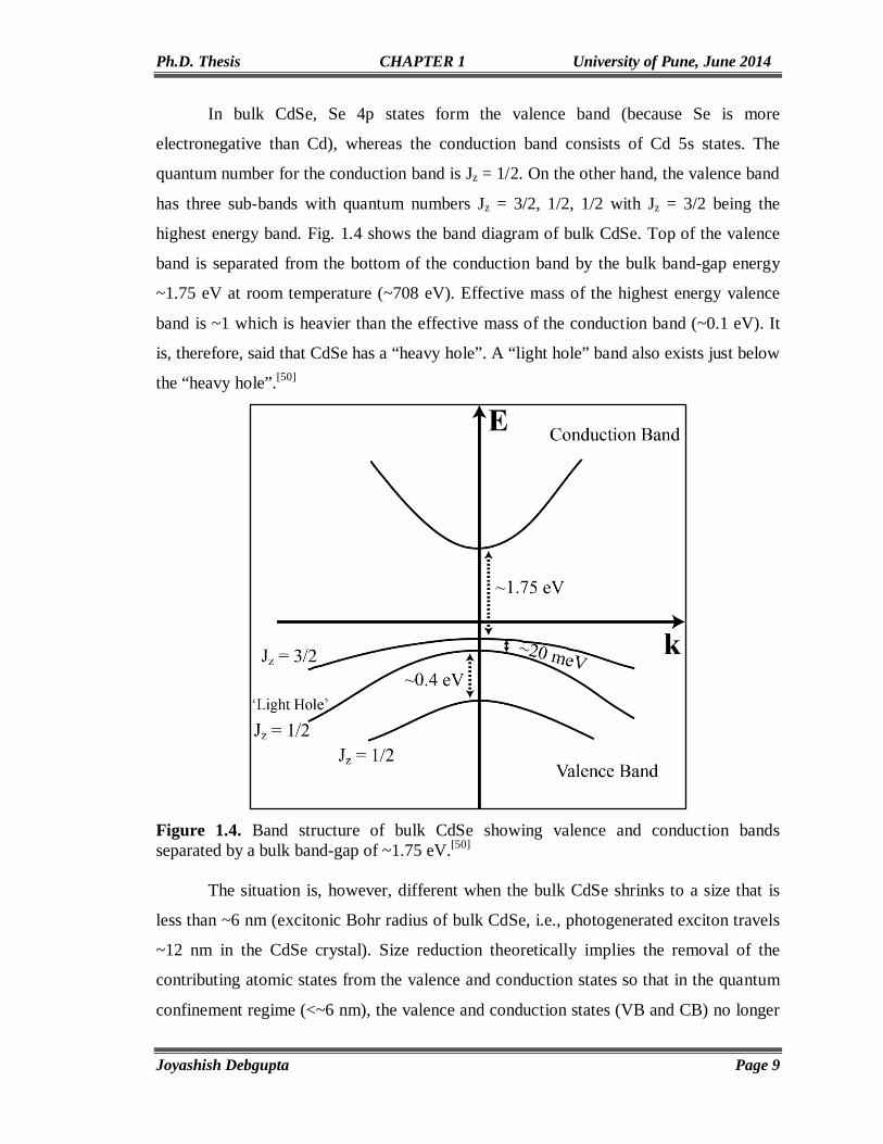
In bulk CdSe, Se 4p states form the valence band (because Se is more
electronegative than Cd), whereas the conduction band consists of Cd 5s states. The
quantum number for the conduction band is Jz = 1/2. On the other hand, the valence band
has three sub-bands with quantum numbers Jz = 3/2, 1/2, 1/2 with Jz = 3/2 being the
highest energy band. Fig. 1.4 shows the band diagram of bulk CdSe. Top of the valence
band is separated from the bottom of the conduction band by the bulk band-gap energy
~1.75 eV at room temperature (~708 eV). Effective mass of the highest energy valence
band is ~1 which is heavier than the effective mass of the conduction band (~0.1 eV). It
is, therefore, said that CdSe has a “heavy hole”. A “light hole” band also exists just below
the “heavy hole”.[50]
Figure 1.4. Band structure of bulk CdSe showing valence and conduction bands separated by a bulk band-gap of ~1.75 eV.[50] The situation is, however, different when the bulk CdSe shrinks to a size that is
less than ~6 nm (excitonic Bohr radius of bulk CdSe, i.e., photogenerated exciton travels
~12 nm in the CdSe crystal). Size reduction theoretically implies the removal of the
contributing atomic states from the valence and conduction states so that in the quantum
confinement regime (<~6 nm), the valence and conduction states (VB and CB) no longer
Ph.D. Thesis CHAPTER 1 University of Pune, June 2014
Joyashish Debgupta Page 10
remain bands, rather they turn into discrete atom like states. But, the VB and CB still
consist of Se 4p and Cd 5s atomic states. The immediate effect of quantum confinement
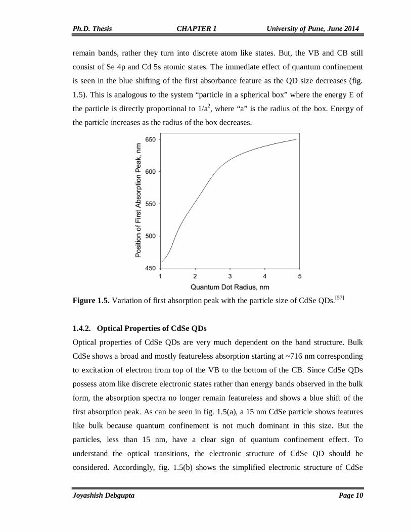
is seen in the blue shifting of the first absorbance feature as the QD size decreases (fig.
1.5). This is analogous to the system “particle in a spherical box” where the energy E of
the particle is directly proportional to 1/a2, where “a” is the radius of the box. Energy of
the particle increases as the radius of the box decreases.
Figure 1.5. Variation of first absorption peak with the particle size of CdSe QDs.[57]
1.4.2. Optical Properties of CdSe QDs
Optical properties of CdSe QDs are very much dependent on the band structure. Bulk
CdSe shows a broad and mostly featureless absorption starting at ~716 nm corresponding
to excitation of electron from top of the VB to the bottom of the CB. Since CdSe QDs
possess atom like discrete electronic states rather than energy bands observed in the bulk
form, the absorption spectra no longer remain featureless and shows a blue shift of the
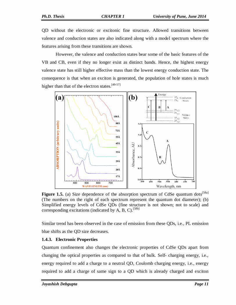
first absorption peak. As can be seen in fig. 1.5(a), a 15 nm CdSe particle shows features
like bulk because quantum confinement is not much dominant in this size. But the
particles, less than 15 nm, have a clear sign of quantum confinement effect. To
understand the optical transitions, the electronic structure of CdSe QD should be
considered. Accordingly, fig. 1.5(b) shows the simplified electronic structure of CdSe
Ph.D. Thesis CHAPTER 1 University of Pune, June 2014
Joyashish Debgupta Page 11
QD without the electronic or excitonic fine structure. Allowed transitions between
valence and conduction states are also indicated along with a model spectrum where the
features arising from these transitions are shown.
However, the valence and conduction states bear some of the basic features of the
VB and CB, even if they no longer exist as distinct bands. Hence, the highest energy
valence state has still higher effective mass than the lowest energy conduction state. The
consequence is that when an exciton is generated, the population of hole states is much
higher than that of the electron states.[49-57]
Figure 1.5. (a) Size dependence of the absorption spectrum of CdSe quantum dots[58a] (The numbers on the right of each spectrum represent the quantum dot diameter); (b) Simplified energy levels of CdSe QDs (fine structure is not shown; not to scale) and corresponding excitations (indicated by A, B, C).[58b]
Similar trend has been observed in the case of emission from these QDs, i.e., PL emission
blue shifts as the QD size decreases.
1.4.3. Electronic Properties
Quantum confinement also changes the electronic properties of CdSe QDs apart from
changing the optical properties as compared to that of bulk. Self- charging energy, i.e.,
energy required to add a charge to a neutral QD, Coulomb charging energy, i.e., energy
required to add a charge of same sign to a QD which is already charged and exciton

Ph.D. Thesis CHAPTER 1 University of Pune, June 2014
Joyashish Debgupta Page 12
ionization energy are three properties which show variation with QD size.[16]These
energies are important because they are responsible for charge transport through the QD
films. Self and Coulomb charging energies are found to increase with decrease in CdSe
QD size just like the blue shift in the absorption. Estimated Coulomb charging energy for
CdSe QD having size <~10 nm, is >100 meV.[59] The available thermal energy at room
temperature (298 K) is ~25 meV which is very less compared to the Coulomb charging
energy of CdSe QDs and so cannot cause conductivity at room temperature.
Consequently, high electric field is required to cause any conduction in a film of CdSe
QDs. Similarly, high electric field is also required to ionize an exciton in CdSe QDs
where exciton ionization energy has been found to be ~100-600 meV.[26]
1.4.4. Coulomb Blockade/Single Electron Transfer
Another interesting consequence of quantum confinement (and discrete atom like states)
is the peculiar “single electron transfer” behavior.[60] Single electron transfer, also known
as “Coulomb blockade”, phenomenon is the addition or subtraction of one electron at a
time to a nanoparticle for charging. In the I-V plot, this behavior is observed as staircase
and so it is also known as “Coulomb staircase” behavior. Klein et al studied single
electron behavior of CdSe QDs by fabricating a single electron transistor.[60]Alperson et
al first showed single electron transport behavior in the electrodeposited film of CdSe
QDs using scanning tunneling spectroscopy (STS) at very low temperature (4.2 K).[61]In
their case, the charging energy (EC) as well as inter-peak spacing have been found to
increase as the dot size decreases. Fig. 1.6 shows the STS plots for the three different
sizes of CdSe QDs showing Coulomb blockade behavior.

Ph.D. Thesis CHAPTER 1 University of Pune, June 2014
Joyashish Debgupta Page 13
Figure 1.6. (a) Tunneling current vs applied voltage (bias) and (b) corresponding conductance spectra of CdSe QDs (2 nm, 3 nm and 4.5 nm) having three different sizes obtained at 4.2 K.[61] 1.5. Synthesis of CdSe Quantum Dots (CdSe QDs)
Numerous synthetic methodologies and processes have been developed during the last
decade for the synthesis of CdSe QDs and various nanostructures of CdSe in general.[62-
64] Of course, the synthetic method to be adopted is highly dependent on the end use of
the QDs. Some of the well-known methods for growing CdSe QDs are discussed in the
following sections.
1.5.1. Solution Synthesis
1.5.1.1. Hot Injection Method (Nonaqueous method)/Colloidal Synthesis
The most successful method of preparing CdSe QDs till to date is the so called “hot
injection synthesis”. Alivisatos, Peng and co-workers successfully synthesized nearly
monodispersed II-VI semiconductor nanoparticles by employing different cadmium (Cd)
precursors in trioctylphosphine oxide (TOPO).[65-66]Various other Cd-precursors have
been for this type of synthesis. Briefly, in this method Cd-precursor (CdO, Cd(OAc)2,
Cd(CH3)2) is allowed form a complex with the capping agents (TOPO, oleic acid, stearic
acid etc.) at temperatures ranging from 250 to 350°C. When proper temperature is
reached, certain amount of Se precursor (made by dissolving Se powder in either TOP or

Ph.D. Thesis CHAPTER 1 University of Pune, June 2014
Joyashish Debgupta Page 14
TBP by slight warming) is injected while the solution is still hot. Immediate drop in
temperature occurs and nucleation sets in. On keeping at this temperature for sometime,
the solution changes color from light yellow to deep red indicating the formation of CdSe
QDs. The color change is generally due to the gradual increase in particle size. This
method gives highly mono-dispersed, crystalline QDs. By choosing appropriate precursor
concentration, solvent, temperature and growth time, QDs of particular size, shape and
concentration can be obtained. Fig. 1.7 is the schematic representation of the overall
process.
Figure 1.7. A schematic representation of the hot-injection method, with the low resolution TEM image of the so formed monodispersed CdSe QDs below. (present work)
Ph.D. Thesis CHAPTER 1 University of Pune, June 2014
Joyashish Debgupta Page 15
1.5.1.2. Low Temperature Aqueous Method
This can be regarded as the aqueous version of the hot-injection method. This works at
relatively low temperature. Cd-precursors used are water soluble Cd-salts such as CdCl2,
Cd(OAc)2, Cd(NO3)2, Cd(ClO4)2 etc; whereas Se-precursor used are Na2SeO3, NaHSe,
Na2SeSO3 etc. Common capping agents are 3-mercaptopropionic acid, 2-
mercaptoethanol, thioglycolic acid etc. which are also water soluble. The process is
highly pH sensitive. The only limitation of this method is that the CdSe QDs obtained are
of slightly inferior optical quality than those obtained in the hot injection method.
1.5.1.3. Electrochemical Method
Electrodeposition is perhaps one of the easiest and more controllable method of CdSe QD
synthesis, because the quality, phase and particle size of the deposit can be controlled by
changing merely the deposition potential or the current density using modern
potentiostats or galvanostats. Different groups have used different composition of solute
and solvent for electrodeposition of CdSe. For example, Fawcett and Baranski have
employed a composition of 100 mL DMF, 1 g CdCl2, 1 g KI and saturated Se solution to
deposit CdSe while [67]KI is used to make the electrodeposited film smooth and coherent.
CdSe deposition has also been carried out from acidic solution which contains CdSO4 as
Cd and SeO2 as Se source.[68-72]CdSe has also been deposited from alkaline bath
containing CdO, NaOH, NaCN, SeO2 and Triton X-100 surfactant for better adhesion and
quality of the deposit.[68],[73] Again, Golan et al have electrodeposited epitaxial CdSe QDs
of 5 nm size on evaporated Au (111) film from DMSO.[74] They have also shown the
formation of rock-salt CdSe structure (8-coordinated) which otherwise is known to be a
metastable phase and occurs at high pressure only.[75] In an another interesting approach,
Mastai et al prepared CdSe QDs by sono-electrochemical method where simultaneous
application of ultrasonication and electrochemical potential led to almost uniform size
distribution of CdSe QDs.[76] However, the major limitation of this method is that it
requires conducting substrate for deposition and so is of limited use in electronics.
1.5.1.4. Hydrothermal/Solvothermal Method
This process generally involves reactions in a closed system in the presence of a solvent
(aqueous or non-aqueous) at its supercritical temperature (i.e., temperature higher than
the boiling point of the solvent).[77] In 1990s, Qian, Li and co-workers developed this
Ph.D. Thesis CHAPTER 1 University of Pune, June 2014
Joyashish Debgupta Page 16
milder, more convenient route of 1D nanostructures of metal chalcogenide of formula,
ME (M = Zn/Cd, E = S/Se) at relatively low temperature.[78-79] They studied several
solvent systems including water for the reaction but CdE (E = S/Se) could only form in
coordinating amine solvents (such as diethylamine, ethylenediamine, pyridine and 1,6-
diaminohexane) by the elemental reaction between Cd and chalcogen at relatively low
temperature.[80] Moreover, it is found that CdSe nanoparticles are only obtained when
pyridine or diethylamine are used as solvents, whereas ethylenediamine leads to nanorod
morphology.[81] Peng and co-workers successfully synthesized wurtzite CdSe QDs using
Cd(NO3)2.4H2O, Na2SeO3 and N2H4.H2O as reactants in NH3.H2O complexation system
and found that the phase of CdSe could be tuned from wurtzite to zinc blende by simply
changing the complexation system from NH3.H2O to EDTA.[82] Even more interesting is
the solvothermal preparation of dodecanethiol capped, nearly monodispersed, large scale
synthesis of 3 nm CdSe QDs by Gautam et al. Cd-stearate and H2Se were the source of
Cd and Se respectively. H2Se was generated in situ by the reaction of elemental Se with
tetralene which in turn becomes aromatic by losing a proton.[83]
1.5.2. Solid State Synthesis
This type of synthesis does not involve any chemical reaction in solution phase; rather all
the reactions do take place in solid state and by physical forces such as heat, mechanical
energy, pressure etc.
1.5.2.1. Mechano-chemical Method
CdSe QDs have been prepared by ball milling elemental Cd and Se under Ar-atmosphere
to protect the CdSe.[84]This type of CdSe QDs have an average particle size of 35 nm.
1.5.2.2. Vapor Deposition Method
Vapor deposition methods are of two types-physical vapor deposition (PVD) and
chemical vapor deposition (CVD). Although very few reports are there on PVD and CVD
for CdSe synthesis, these techniques often lead to different nanostructure other than
spherical CdSe. For example, CdSe nanobelts and nanosaws have been prepared by PVD
method employing CdSe powder which was sublimed at 750°C and subsequently
deposited on gold nanoparticles (3-5 nm) decorated single crystalline Si-substrate.[85]
On the other hand, single crystalline CdSe nanobelts have been prepared by
Venugopal et al by a CVD method assisted by laser ablation by employing CdSe powder
Ph.D. Thesis CHAPTER 1 University of Pune, June 2014
Joyashish Debgupta Page 17
as source.[86] Similarly, various nanostructures of CdSe have been prepared by Zhang et
al using Si-assisted CVD process.[87]Although the processes give good yield of the
nanostructured products, they suffer from limitations of employing high temperature
and/or costly apparatus which automatically increase the cost of production in large scale
as is required for the industry. Maintaining proper gas flow rate, type of precursors, rate
of heating and cooling can also affect the selectivity and yield of these processes
significantly.
1.5.2.3. Molecular Beam Epitaxy (MBE) and Gas Phase Methods
Molecular beam epitaxy (MBE) is one of the several methods of depositing single
crystals. MBE is widely used in the manufacture of semiconductor devices,
including transistors for cellular phones and WiFi. Self assembling growth of CdSe QDs
has been reported by Xin et al during MBE on ZnSe and ZnMnSe. The so formed CdSe
QDs are uniform in size with an average diameter of 40±5 nm.[88]
Some reports are also there for the gas phase synthesis of CdSe QDs by
decomposing some volatile precursors. For example, volatile chalcogenolato complexes
of cadmium with stertically demanding thio- and selenophenolato ligands have been
synthesized by Bochmann et al. These complexes decompose at temperature >350°C to
form thin film of CdSe QDs.[89] Organic vapor phase epitaxy has also been used to make
CdSe QD film by employing dimethylcadmium and H2Se as the precursors for Cd and Se
respectively.[90]Atomic Layer Deposition (ALD) is another gas phase technique for the
deposition of conformal film of CdSe. This consists of sending the Cd and Se from their
respective elemental source consecutively with a dead time between the vapor pulses to
stabilize the surface and to re-evaporate the possible excess material. The sequence of
steps forms one complete ALD cycle. ALD differs from MBE in the fact that the
constitutive elements are brought onto the surface together (at the same time) in case of
MBE. ALD gives much better control on the morphology of the deposited film as
compared to MBE.
Table 1.1 lists merits and demerits of all the synthetic procedures described.

Ph.D. Thesis CHAPTER 1 University of Pune, June 2014
Joyashish Debgupta Page 18
Table 1.1. Comparison of the synthesis methods used for the synthesis of CdSe QDs
Method Advantage Limitation Reference
Colloidal Synthesis Uniform particle size, good quantum yield
Poor yield per batch [64-66]
Electrochemical
Synthesis
Very easy, can be performed in ambient condition
Difficult for very small QDs (~1-3 nm), often results in dendritic growth
[67-72]
Hydrothermal
Synthesis
Yield is good, easy process, common precursors
Non-uniform particle size distribution, higher surface defects
[77-79]
Mechano Chemical
Synthesis
Room temperature synthesis
Bigger particle size (~35 nm), poor optical properties
[84]
Vapor Deposition
Methods (ALD,
MBE, CVD)
Very good control over product and/or film
High temperature process, costly accessories in some methods (MBE, ALD), slow process
[85-87]
1.6. Applications of CdSe Quantum Dots
Due to its unique features like direct band-gap and excellent photoelectrical properties,
CdSe finds many applications starting from optoelectronic devices to transistors, sensors
and even biological labelling.
1.6.1. Solar Cells
CdSe is an important material for solar photovoltaic applications because of its low band-
gap and good transport properties. Consequently, CdSe QDs are used in following three
different ways in solar cells:
(i) It can be used as a carrier transport material because it covers almost the entire
solar spectrum. For example, colloidal CdSe nanorods have been used in bilayer
nanocrystal solar cells which shows power conversion efficiency of 3%.[91]Again,
Kuno et al have found that the addition of CdSe QDs to CdSe nanowires solar cell
enhances the power conversion efficiency from 13% to 25% at 500 nm.[92]
Recently, Cao et al have developed solar cell based on CdSe nanobelt and CNT

Ph.D. Thesis CHAPTER 1 University of Pune, June 2014
Joyashish Debgupta Page 19
which act as both transparent medium to allow passage of light as well as
provides a conducting pathway for transporting the photo-generated electrons to
the current collectors.[93] A similar strategy has been also adopted to make solar
cell employing CdSe nanobelt and graphene.[94]
(ii) CdSe QDs can be decorated on inorganic nanostructures such as TiO2 or ZnO
nanoparticles for quantum dot sensitized solar cells (QDSSCs). Due to its tunable
optical properties, CdSe QDs or nanostructures in general can function as efficient
sensitizer through the entire visible region.[95] For example, CdSe QD decorated
TiO2 nanotube arrays has been shown to give an efficiency as high as 4.15%.[96]
(iii) Hybrids of CdSe QDs and conjugate polymers are also an interesting materials for
solar cells because they allow the unique optoelecronic properties of organic
semiconductors to be coupled with the intriguing properties of CdSe QDs.
Accordingly, CdSe nanorods with good hole transporting polymer P3HT have
been utilized in fabricating nanorod-polymer blend solar cell with external
quantum efficiency as high as 59% under 0.1 mWcm-2 illumination at 450 nm.[97]
1.6.2. Photodetectors
Photodetectors are a class of important optoelectronic device which are used for photon
detection in the UV or IR region. This has so many practical applications such as
biological diagnostics, chemical sensors, missile launch and light-wave communications.
The heart of a photodetector is a semiconductor which absorbs light with higher energy
than the band-gap energy of the semiconductor.[98] CdSe, being a direct and low band-gap
semiconductor material, is an ideal candidate for photodetectors. For example, a
photodetector has been successfully prepared using CVD grown CdSe nanoribbons. The
device shows photoconductance of the CdSe nanoribbons to be 2816 nS at 650 nm and
0.095 nS in the dark condition.[99]
1.6.3. Light Emitting Diodes (LEDs)
Light emitting diodes (LEDs) are solid state devices. Much attention is now being
focused for the development of low cost, highly efficient LEDs of different color,
especially a need exists for white light LEDs in order to replace the conventional light
source. High quality CdSe QDs has high quantum efficiency and the size can be tuned so
Ph.D. Thesis CHAPTER 1 University of Pune, June 2014
Joyashish Debgupta Page 20
as to control their emission within 500 and 650 nm. So CdSe QDs are interesting as LED
material. For example, Rosenthal et al demonstrated white light emission from ultra small
CdSe QDs.[100-101]These ultra-small CdSe QDs show emissions from 420-710 nm
(broadband emission) without suffering the problem of self-absorption. CdSe QDs have
also been utilized as the red emitting counterpart in LEDs. For example, Jeon et al have
recently synthesized greenish-yellow emitting Sr3SiO5:Ce3+, Li+ and high quality
TOP/TOPO/HAD-capped CdSe QDs. They fabricated a LED which can render good
colors, by coating the two luminescent materials on a blue LED chip.[102]
1.6.4. Biological Applications
Long lived, stable, narrow PL is the key feature which makes CdSe QDs attractive for
biologists. Its intrinsic PL has been widely exploited for bio-imaging. CdSe QDs have
also been used for biosensors. Nocera et al systematically reviewed the applications of
CdSe QDs as biosensors.[103-105]
Moreover, CdSe QDs have also been employed in other applications such as
emitters for color displays,[106]optical fiber amplifiers,[107] low threshold lasers, self
assembled photonic sphere arrays, optical temperature probes, chemical sensors,[108] etc.
1.7. Conclusions and Perspectives
Some of the most interesting developments of CdSe QDs and its hybrid nano-structures
are reviewed in this chapter with special emphasis on the synthesis, properties and
various applications. Theory along with experimental evidence suggests intriguing
structure and size as well as shape dependent optical and electronic properties of these
semiconductor nanoparticles. Presence of discrete, atom like states in QDs has profound
impact on nanoelectronics, especially for designing single electron transistors, single
photon counting devices etc. Also, having vast tunability with respect to their structure
and property, these applications are expected to lead the prospect of this field for
continuing decades perhaps, with immense benefits in many areas like energy, healthcare
and environmental monitoring. More precisely, they act as the building blocks for
hierarchical, multifunctional, tailor-made materials with potential applications in our day-
to-day life. However, although there are so many methods available for the synthesis and
applications of CdSe QDs and the hybrids, several daunting challenges of these materials
Ph.D. Thesis CHAPTER 1 University of Pune, June 2014
Joyashish Debgupta Page 21
such as development of low cost, synthetic methods, scale up synthesis as well as ease of
fabrication of devices requires breakthrough results for the sake of technology.
1.8. Motivation, Scope and Organization of the Thesis
The genesis of the present thesis is inspired by many of the interesting issues unraveled
during the preparation of the above critical review related to both fundamental and
applied aspects of CdSe QDs and its hybrids. This includes the development of novel
approaches to synthesize CdSe QDs directly on graphene or graphene nanoribbons
(GNRs), followed by their detailed characterizations. If processed properly, these QDs
and also their hybrids can open up new avenues for various unprecedented applications.
As a consequence, it is imperative to study different properties such as optical,
electrochemical, wetting for the pursuit of various applications.
1.9. Objectives of the Present Investigation
The present thesis attempts to address some of the above challenges by designing new
synthetic methodologies followed by chemical and electrochemical characterization.
More specifically, the objectives of the thesis are set as follows:
(i) To study the band structure parameters (HOMO-LUMO positions) of CdSe QDs
of different sizes by various electrochemical techniques starting from cyclic
voltammetry (CV), differential pulse voltammetry (DPV), chronoamperometry
and electrochemical impedance spectroscopy.
(ii) To study the wetting properties of CNTs with various liquids including water.
(iii) To generate CdSe QDs electrochemically directly on graphene nanoribbons
obtained from unzipping of CNTs and characterization of the hybrids.
(iv) To develop new methodology to make thiol terminated graphene using diazonium
salt chemistry and using it to anchor CdSe QDs.
(v) To study the excited state charge transfer dynamics of CdSe QDs and those
attached to thiol modified graphene.
(vi) To study the photovoltaic properties of the CdSe QD-thiolated graphene hybrids.
(vii) To synthesize CdSe nanotubes by ZnO template assisted electrodeposition for the
fabrication of a n-p heterojunction diode for optoelectronic applications.
The present thesis consists of six chapters which discuss few novel methods of preparing
CdSe and its hybrids with carbon based materials, namely CNTs and graphene as well as
Ph.D. Thesis CHAPTER 1 University of Pune, June 2014
Joyashish Debgupta Page 22
with p-type Cu2O, their detail characterizations using various techniques followed by
potential applications in case of energy generation. Chapter 1 is a critical survey of
Quantum dots and CdSe QDs in particular. Variation in optical as well as electronic
properties with variation in size and shape has been discussed with little theoretical
discussion. The chapter also discusses various synthetic methods available so far for the
synthesis of CdSe QDs along with special emphasis on various characterization
techniques starting from spectroscopic and microscopic to electrochemical techniques.
Finally, the potential applications of these QDs for solar cells, photodetectors, water
splitting etc. have been introduced. The chapter concludes by setting up the specific
objectives for the present study, future prospects and finally mentioning some of the
existing limitations of these QDs and QD based hybrid nanomaterials.
Chapter 2 illustrates the electrochemical properties of CdSe QDs of varying size. The
prepared QDs have been characterized by various techniques starting from UV-Vis, PL,
powder X-ray diffraction (PXRD) to light scattering techniques. Absolute band positions
of these QDs along with their electrochemical bandgap variation have been studied in
detail by various electrochemical techniques starting from cyclic voltammetry,
differential pulse voltammetry and impedance techniques.
Chapter 3 is about the exploratory behavior of QDs attached to carbon nanostructures,
especially carbon nanotubes and graphene nanoribbons. More specifically, single walled
carbon nanotube (SWCNT) surface is modified with –PhSH group with the help of
diazonium functionalization in order to anchor oleic acid capped CdSe QDs viaa simple
solution exchange methodology. Wetting behavior of pristine as well as functionalized
CNTs is studied with water and various organic liquids. Electrochemical properties of the
QD-CNT/GNR hybrids are studied with DPV, CV and impedance. In the next part of the
chapter CdSe QDs have been decorated on graphene nanoribbons (GNRs) obtained from
the electrochemical unzipping of SWCNTs to understand the properties of CdSe QDs in
presence of quasi 2-D carbon sheet. GNR is chosen because it’s band structure and
properties are different as compared to that of CNT or graphene (2-D). More
interestingly, the width of the GNR has a profound effect on its band structure in
controlling the edge-states. The resulting hybrid has been characterized using various
Ph.D. Thesis CHAPTER 1 University of Pune, June 2014
Joyashish Debgupta Page 23
techniques starting from PXRD, UV-Vis, PL to electrochemical techniques. Micro
Raman has been used extensively to study the unzipping process of SWCNT and
subsequent CdSe QD attachment via electrochemical technique. Photoconductivity study
has been carried out to explore these materials as potential candidates for 3rd generation
solar cells, photodetectors and other optoelectronic devices.
Chapter 4 illustrates the study of the hybrid consisting of CdSe QDs attached to
Graphene (a real 2-D system) via –PhSH linker group. This chapter is divided into two
parts. In the first part of the chapter, Graphene, derived from the reduction of graphene
oxide with NaBH4, surface is modified with –PhSH group with the help of diazonium
functionalization followed by the attachment of oleic acid capped CdSe QDs viaa simple
solution exchange methodology. The resulting hybrid has been studied with various
characterization techniques such as FTIR, elemental mapping, cyclic voltammetry,
impedance technique, contact angle measurement, micro Raman, UV-Vis, steady state
PL, TEM and XPS. The strategy has been unique in facilitating monodisperse, predefined
size CdSe QDs to be arranged on 2-D plane of graphene with the help of very simple
solution chemistry. XPS result confirms the binding of CdSe to the –SH group on
graphene surface. In the second part, ultrafast charge carrier dynamics study has been
carried out in order to understand charge transfer from excited CdSe QDs to –PhSH
functionalized graphene. Time resolved photoluminescence measurement has been
carried out along with steady state PL for this purpose. Charge transfer has been found to
be the major pathway for the deactivation of excited QDs in presence of –SH
functionalized graphene and the rate of electron transfer has been estimated as high as
~13 x 108 s-1. Moreover, a prototype bulk hetero-junction has been made out of this
hybrid employing PEDOT:PSS as a hole-conducting layer and it is found to show good
photoconductivity in presence of AM 1.5 solar simulated light. This again proves the use
of this hybrid-material for solar cells and other optoelectronic devices. The chapter ends
with the conclusion of developing a new hybrid system for potential solar applications.
Chapter 5 describes the electrochemical synthesis of vertically aligned CdSe nanotubes
on conducting glass substrates (FTO). In order to facilitate this ZnO NWs have been
grown first on FTO plates using hydrothermal method followed by electrodeposition of

Ph.D. Thesis CHAPTER 1 University of Pune, June 2014
Joyashish Debgupta Page 24
CdSe on ZnO NWs. Removal of the ZnO core results in hollow, vertically aligned CdSe
nanotubes which retain the morphology of ZnO NW templates. SEM, TEM,
electrochemical techniques, micro Raman, UV-Vis, PL are used to characterized the
materials. Next, p-type Cu2O film has been electrodeposited on FTO plates from a
copper-lactate bath. The two FTO plates-one containing CdSe nanotubes and another
containing Cu2O, are then brought in intimate contact with each other in a flip-chip
geometry. I-V measurement shows the formation n-p type hetero-junction at the
interface. The resulting hetero-junction shows good photoconductivity in presence of AM
1.5 solar simulated light. Further, a threefold increment in conductivity has been
observed for this system in presence of light, thereby proving the system to be a good
photon harvesting device. The role of individual interface and shape and size dependant
performance parameters are discussed on the basis of I-V plots.
Chapter 6 is a summary of all the major conclusions of the present study with respect to
the preparation, characterization, properties and potential applications of these hybrid
nanomaterials. It also indicates the possible advantage of CdSe and CdSe based hybrid
nanostructures for the fabrication of next generation optoelectronic devices with the
much sought flexibility in the resulting devices. This chapter also outlines some of the
limitations of this electrochemical synthesis along with ample scope of further work in
this area and its bright future prospects.
The results presented in the thesis clearly suggest the usefulness of CdSe QDs and
its hybrid nanostructures as multifunctional materials for many industrial applications
like solar cells, nanoelectronics and biological imaging. The possibility of manipulating
the optical properties as well as electron transfer characterisics of CdSe QDsby
combining with different materials (particularly carbonaceous nanomaterials) has also
been demonstrated which is expected to resolve several important issues related to
fundamental properties of CdSe QDs and their interactions with hybrids. The insights
obtained from these are valid for all types of quantum dots, which could be of immense
utility in designing new materials with improved performance attributes.

Ph.D. Thesis CHAPTER 1 University of Pune, June 2014
Joyashish Debgupta Page 25
1.10. References
1. (a) Kurtoglu, M. E.; Longenbach, T.; Reddington, P.; Gogotsi, Y. J. Am. Ceram. Soc.
2011, 94 (4), 1101. (b) Ge, L.; Sethi, S.; Ci, L.; Ajayan, P. M.; Dhinojwala, A. Proc.
National Acad. Sciences 2007, 104, 10792. (c) "Nanotechnology Consumer
Products". nnin.org. 2010, Retrieved April 21, 2014. (d) "Nanotechnology
Information Center: Properties, Applications, Research, and Safety Guidelines".
American Elements. Retrieved April 21, 2014. (e)
http://www.azonano.com/article.aspx?ArticleID=3396, Retrived April 21, 2014. (f)
Shulaker, M. M.; Hills, G.; Patil, N.; Wei, H.; Chen, H.-Y.; Wong, H.-S. P.; Mitra, S.
Nature 2013, 501, 526. (g) http://www.sigmaaldrich.com/materials-
science/nanomaterials/gold-nanoparticles.html, Retrived April 21, 2014. (h) Wang,
S.; Jiang, L. Adv. Mater. 2007, 19, 3423. (i) Young, T. Phil. Trans. R. Soc. Lond.
1805, 95, 65. (j) Wenzel, R. N. Ind. Eng. Chem. 1936, 28, 988. (d) Extrand, C.
Langmuir 2005, 68, 2495. (k) Johnson, R E.; Dettre, R. H. J. Phys. Chem. 1964, 68,
1744. (l) Onda, T.; Shibuichi, S.; Satoh, N.; Tsujii, K. Langmuir 1996, 12, 2125. (m)
Miwa, M.; Nakajima, A.; Fujishima, A.; Hashimoto, K.; Watanabe, T. Langmuir
2000, 16, 5754. (n) Shirtcliffe, N. J.; McHale, G.; Newton, M. I.; Perry, C. C.
Langmuir 2003, 19, 5626. (o) Teare, D.; Spanos, C. G.; Ridley, P.; Kinmond, E. J.;
Roucoules, V.; Badyal, J. P. S.; Brewer, S. A.; Coulson, S. Chem. Mater. 2002, 14,
4566. (p) Bico, J.; Marzolin, C.; Quere, D. Europhys. Lett.1999, 47, 743. (q) Extrand,
C. MRS Bulletin 2008, 733. (r) Gao, L. C.; McCarthy, T. J. Langmuir 2007, 23, 3762.
(s) Chen, W.; Fadeev, A. Y.; Hsieh, M. C.; Oner, D.; Youngblood, J.; McCarthy, T. J.
Langmuir 1999, 15, 3395. (t) Wang, S. T.; Liu, H.; Jiang, L. Ann. Rev. Nano Res.
2006, 1, 573. (u) Lim, H. S.; Kwak, D.; Lee, D. Y.; Lee, S. G.; Cho, K. J. Am. Chem.
Soc. 2007, 129, 4128. (v) Xue, C. H. Sci. Technol. Adv. Mater. 2008, 9, 035008. (w)
Xue, C. H. Sci. Technol. Adv. Mater. 2008, 9, 035001. (x) Yuan, Z. Sci. Technol. Adv.
Mater. 2008, 9, 045007. (y) Ressine, A.; Marko-Varga, G.; Laurell, T. Biotechnol.
Ann. Rev. 2007, 13, 149.
2. (a) Zhen, H. L.; Donald G. T. J. Am. Chem. Soc. 2008, 130, 12698. (b) Nagarajan, R.
ACS Symposium Series 2008, 996, 2. (c) Drexler, E. Enginesof Creation: The Coming
Era of Nanotechnology; Anchor Press/ Doubleday: New York, 1986. (d) Drexler, K.

Ph.D. Thesis CHAPTER 1 University of Pune, June 2014
Joyashish Debgupta Page 26
E. Nanosystems: molecular machinery, manufacturing and computation; John Wiley
& Sons: New York, 1992. (e) Kohler, M.; Fritzsche, W. Nanotechnology, An
Introduction to Nanostructuring Techniques, Wiley-VCH Verlag GmbH and Co.
KgaA, 2004.
3. (a) West, A. R. Solid State Chemistry and Its Applications. ISBN: 978-0-471-90874-
6. (b) Cottey A. A. J. Phys. C: Solid State Phys.1971, 4, 1734.
4. (a) Rao, C. N. R.; Thomas, P. J.; Kulkarni, G. Nanocrystals:: Synthesis, Properties
and Applications, Vol. 95, Springer 2007. (b) Leutwyler, W. K.; Bürgi, S. L.; Burgl,
H. Science 1996, 271, 933. (c) Alvisatos, A.P. Science 1996, 271, 933.
5. Alivisatos, A. P. J. Phys. Chem. 1996, 100, 13226.
6. Vossmeyer, T.; Katsikas, L.; Giersig, M.; Popovic, I.; Diesner, K.; Chemseddine, A.;
Eychmüller, A.; Weller, H. J. Phys. Chem. 1994, 98, 7665.
7. Leutwyler, W. K.; Bürgi, S. L.; Burgl, H. Science 1996, 271, 933.
8. Goldstein, A.; Echer, C.; Alivisatos, A. Science 1992, 256, 1425.
9. Tolbert, S. H.; Alivisatos, A. Annu. Rev. Phys. Chem.1995, 46, 595.
10. Buhro, W. E.; Colvin, V. L. Nature materials 2003, 2, 138.
11. (a) Maksym, P.; Chakraborty, T. Phys. Rev. Lett.1990, 65, 108. (b) Chakraborty, T.
Matter Phys. 1992,16, 35; Maksym, P. A.; Chakraborty T. Phys. Rev. Lett. 1990, 65,
108. (c) Chakraborty, T.: Quantum Dots: A survey of the properties of artificial
atoms; Elsevier, 1999. (d) Kasfner, M. A.: Artificial atoms. Physics today 1993, 25.
(e) Reed, M. A. Scientific American 1993, 268, 118. (f) Leutwyler, W. K.; Bürgi, S.
L.; Burgl, H. Science 1996, 271, 933. (g)Ashoori, R. Nature 1996, 379, 413. (h)
McEuen, P. L. Science 1997, 278, 1729. (i) Gammon, D. Nature 2000, 405, 899.
12. (a) Ekimov, A. I.; Onushchenko, A. A.Fiz. Tekh. PoluproVodn.1982, 16, 1215
(Translation: SoV. Phys. Semicond. 1982, 16, 775). (b) Rossetti, R.; Nakahara, S.;
Brus, L. J. Chem. Phys. 1983, 79, 1086.
13. Kittel, C.; McEuen, P.: Introduction to solid state physics; Wiley New York, 1986;
Vol. 8.
14. Efros, A. L.; Rosen, M. Annu. Rev. Mater. Sci. 2000, 30, 475.
15. Efros, A. L.; Efros, A. L. Soviet Physics Semiconductors-Ussr 1982, 16, 772.
16. Brus, L. J. Chem. Phys. 1983, 79, 5566.

Ph.D. Thesis CHAPTER 1 University of Pune, June 2014
Joyashish Debgupta Page 27
17. Brus, L. E. J. Chem. Phys. 1984, 80, 4403.
18. Dabbousi, B. O.; Rodriguez-Viejo, J.; Mikulec, F. V.; Heine, J. R.; Mattoussi, H.;
Ober, R.; Jensen, K. F.; Bawendi, M. G. J. Phys. Chem. B 1997, 101, 9463.
19. http://www.nanocrystals.nl/Photos.HTML (last retrieved on 29th March, 2014).
20. Nirmal, M.; Dabbousi, B.; Bawendi, M.; Macklin, J.; Trautman, J.; Harris, T.; Brus,
L. Nature 1996, 383, 802.
21. Fisher, B. R.; Eisler, H.-J.; Stott, N. E.; Bawendi, M. G. J. Phys. Chem. B 2004, 108,
143.
22. Leatherdale, C. A.; Woo, W. -K.; Mikulec, F. V.; Bawendi, M. G. J. Phys. Chem.
B 2002, 106 (31), 7619.
23. Nozik, A. J. Chem. Phys. Lett. 2008, 457, 3.
24. (a) Coe-Sullivan, S.; Woo, W.-K.; Steckel, J. S.; Bawendi, M.; Bulović, V. Org.
Electron.2003, 4, 123. (b) Coe, S.; Woo, W.-K.; Bawendi, M.; Bulović, V. Nature
2002, 420, 800. (c) Colvin, V.; Schlamp, M.; Alivisatos, A. Nature 1994, 370, 354.
(d) Dabbousi, B.; Bawendi, M.; Onitsuka, O.; Rubner, M. Appl. Phys. Lett.1995, 66,
1316.
25. (a) Eisler, H.-J.; Sundar, V. C.; Bawendi, M. G.; Walsh, M.; Smith, H. I.; Klimov, V.
Appl. Phys. Lett.2002, 80, 4614. (b) Sundar, V. C.; Eisler, H. J.; Bawendi, M. G. Adv.
Mater.2002, 14, 739.
26. (a) Bawendi, M. G.: The electronic and optical properties of close packed cadmium
selenide quantum dot solids. Massachusetts Institute of Technology, 1996. (b)
Leatherdale, C.; Kagan, C.; Morgan, N.; Empedocles, S.; Kastner, M.; Bawendi, M.
Phys. Rev. B 2000, 62, 2669. (c) Jarosz, M.; Stott, N.; Drndic, M.; Morgan, N.;
Kastner, M.; Bawendi, M. J. Phys. Chem. B 2003, 107, 12585. (d) Drndić, M.; Jarosz,
M.; Morgan, N.; Kastner, M.; Bawendi, M. J. Appl. Phys. 2002, 92, 7498. (e) Ting,
D. Z.; Soibel, A.; Keo, S. A.; Rafol, S. B.; Mumolo, J. M.; Liu, J. K.; Hill, C. J.;
Khoshakhlagh, A.; Hoeglund, L.; Luong, E. M.; Gunapala, S. D. J. Appl. Remote
Sens. 2014, 8. (f) Chen, M.; Yu, H.; Kershaw, S. V.; Xu, H.; Gupta, S.; Hetsch, F.;
Rogach, A. L.; Zhao, N. Adv. Funct. Mater. 2014, 24, 53. (g) Gustafsson, O.; Karim,
A.; Asplund, C.; Wang, Q.; Zabel, T.; Almqvist, S.; Savage, S.; Andersson, J. Y.;
Hammar, M. Infrared Phys. Technol. 2013, 61, 319. (h) Lao, Y.-F.; Wolde, S.;

Ph.D. Thesis CHAPTER 1 University of Pune, June 2014
Joyashish Debgupta Page 28
Perera, A. G. U.; Zhang, Y. H.; Wang, T. M.; Liu, H. C.; Kim, J. O.; Schuler-Sandy,
T.; Tian, Z.-B.; Krishna, S. S. Appl. Phys. Lett. 2013, 103. (i) Lao, Y.-F.; Wolde, S.;
Perera, A. G. U.; Zhang, Y. H.; Wang, T. M.; Liu, H. C.; Kim, J. O.; Schuler-Sandy,
T.; Tian, Z.-B.; Krishna, S. S. Appl. Phys. Lett. 2013, 103.
27. (a) Miralaie, M.; Leilaeioun, M.; Abbasian, K.; Hasani, M. J. Comput. Theor. Nanos.
2014, 11, 15. (b) See, A. M.; Klochan, O.; Micolich, P.; Aagesen, M.; Lindelof, P. E.;
Hamilton, A. R. J. Phys. Cond. Mat. 2013, 25.
28. Bruchez, M.; Moronne, M.; Gin, P.; Weiss, S.; Alivisatos, A. P. Science 1998, 281,
2013.
29. Taik Lim, Y.; Kim, S.; Nakayama, A.; Stott, N. E.; Bawendi, M. G.; Frangioni, J. V.
Mol. Imaging 2003, 2.
30. Kim, S.; Lim, Y. T.; Soltesz, E. G.; De Grand, A. M.; Lee, J.; Nakayama, A.; Parker,
J. A.; Mihaljevic, T.; Laurence, R. G.; Dor, D. M. Nat. Biotechnol. 2004, 22, 93.
31. Dahan, M.; Laurence, T.; Pinaud, F.; Chemla, D.; Alivisatos, A.; Sauer, M.; Weiss, S.
Opt. Lett. 2001, 26, 825.
32. Kastner, M. A. Physics Today 1993, 46 (24), 24.
33. Moison, J. M.; Houzay, F.; Barthe, F.; Leprince, L.; Andre, E.; Vatel, O. Appl. Phys.
Lett. 1994, 64 (2), 196.
34. Leonard, D.; Krishnamurthy, M.; Reaves, C. M.; Denbaars, S. P.; Petroff, P. M.
Appl. Phys. Lett. 1993 63 (23), 3203.
35. http://en.wikipedia.org/wiki/Cadmium_selenide (last retrieved on 29th March, 2014).
36. Lev Isaakovich Berger (1996). Semiconductor materials. CRC Press. p. 202. ISBN 0-
8493-8912-7.O. Madelung, ed., Crystal and Solid State Physics, Landolt Bornstein
Numerical
37. Data and Functional Relationships in Science and Technology (Springer-Verlag,
Berlin, 1982), Vol. 17b: Physics of II-VI and I-VII Compounds, Semimagnetic
Semiconductors.
38. Peng , Q.; Dong , Y. J.; Demng , Z. X.; Li , Y. D. Inorg. Chem. 2002, 41, 5249.
39. Blanton, S. A.; Dehestani, A.; Guyot-Sionnest, P.; Lin, P. C. Chem. Phys. Lett.1994,
229, 317.

Ph.D. Thesis CHAPTER 1 University of Pune, June 2014
Joyashish Debgupta Page 29
40. Murray, C. B.: Synthesis and characterization of II-IV quantum dots and their
assembly into 3D quantum dot superlattices. Massachusetts Institute of Technology,
1995.
41. Klimov, V. I. Los Alamos Science 2003, 28, 214.
42. Min, S.-K.; Lee, W.; Cai, G.; Lee, M.; Cho, B. W.; Lee, S.-H.; Han, S.-H. J. Nanosci.
Nanotechno. 2009, 9, 7123.
43. Dixit, S. K.; Madan, S.; Kaur, A.; Madhwal, D.; Singh, I.; Bhatnagar, P. K.; Mathur,
P. C.; Bhatia, C. S. J. Renew. Sus. Energy 2013, 5.
44. Mondal, S. P.; Bera, S.; Narender, G.; Ray, S. K. Appl. Phys. Lett. 2012, 101, 173108.
45. Zarazua, I.; De la Rosa, E.; Lopez-Luke, T.; Reyes-Gomez, J.; Ruiz, S.; Angeles
Chavez, C.; Zhang, J. Z. J. Phys. Chem. C 2011, 115, 23209.
46. Kulakovich, O.; Strekal, N.; Yaroshevich, A.; Maskevich, S.; Gaponenko, S.; Nabiev,
I.; Woggon, U.; Artemyev, M. Nano Lett. 2002, 2, 1449.
47. Medintz, I. L.; Uyeda, H. T.; Goldman, E. R.; Mattoussi, H. Nature materials 2005,
4, 435.
48. Ghosh, T.; Cho, K. Y.; Ullah, K.; Nikam, V.; Park, C. Y.; Meng, Z. D.; Oh, W. C. J.
Ind. Eng. Chem. 2013, 19(3), 797.
49. Efros, A. L.; Rosen, M. Phys. Rev. B 1998, 58, 7120. (b)
50. Madelung, O. ed., Crystal and Solid State Physics, Landolt Bornstein Numerical
Data and Functional Relationships in Science and Technology (Springer-Verlag,
Berlin, 1982), Vol. 17b: Physics of II-VI and I-VII Compounds, Semimagnetic
Semiconductors.
51. Guyot-Sionnest, P.; Shim, M.; Matranga, C.; Hines, M. Phys. Rev. B1999, 60, R2181.
52. Guyot-Sionnest, P.; Hines, M. A. Appl. Phys. Lett.1998, 72, 686.
53. Shim, M.; Shilov, S. V.; Braiman, M. S.; Guyot-Sionnest, P. J. Phys. Chem. B 2000,
104, 1494.
54. Shim, M.; Guyot-Sionnest, P. Nature 2000, 407, 981-983.
55. Shim, M.; Wang, C.; Guyot-Sionnest, P. J. Phys. Chem. B 2001, 105, 2369.
56. Wang, C.; Shim, M.; Guyot-Sionnest, P. Appl. Phys. Lett. 2002, 80, 4.
57. Kuno, M. K. "Band Edge Spectroscopy of CdSe QuantumDots," (Massachusetts
Institute of Technology, Cambridge, 1998)
Ph.D. Thesis CHAPTER 1 University of Pune, June 2014
Joyashish Debgupta Page 30
58. (a) Leatherdale, C. A. "Photophysics of CadmiumSelenide QuantumDot Solids,"
(Ph.D. Thesis, Massachusetts Institute of Technology, Cambridge, MA, 2000). (b)
Jarosz, M.: The physics and chemistry of transport in CdSe quantum dot solids.
Massachusetts Institute of Technology, 2004.
59. (a) Romero, H. E.; Drndic, M. Phys. Rev. Lett. 2005, 95, 156801. (b) Shinde, D. B.;
Pillai, V. K. Angew. Chem. Int. Ed. 2013, 52, 2482.
60. Klein, D. L.; Roth, R.; Lim, A. K.; Alivisatos, A. P.; McEuen, P. L. Nature 1997,
389, 699.
61. Alperson, B.; Rubinstein, I.; Hodes, G.; Porath, D.; Millo, O. Appl. Phys. Lett. 1999,
75, 1751.
62. Yu, S.-H.; Yang, J.; Han, Z.-H.; Yang, R.-Y.; Qian, Y.-T.; Zhang, Y.-H. J. Solid State
Chem. 1999, 147, 637.
63. Zhao, L.; Hu, L.; Fang, X. Adv. Funct. Mater.2012, 22, 1551.
64. Manna , L.; Scher , E. C.; Li , L. S.; Alivisatos , A. P. J. Am. Chem. Soc. 2002, 124,
7136.
65. Peng, Z. A.; Peng, X. G. J. Am. Chem. Soc. 2002, 124, 3343.
66. Fawcett, W. R.; Baranski, A. S. 1983. U.S. Pat. No. 4, 376, 682.
67. Hodes, G.; Manassen, J.; Neagu, S.Thin Solid Films 1982, 90 433.
68. Hodes, G.; Manassen, J.; Cahen, D. Nature 1976, 261, 403.
69. Tomkiewicz, M.; Ling, I.; Parsons, S. J. Electrochem. Soc. 1982, 129, 2016.
70. Boudreau, R A.; Rauh, R D. Sol. Energy Mater. 1982 7 385.
71. Vas'ko, A. T.; Tsikovkin, E. M.; Kovach, S. K. U kr. Khim. Zh. 1983, 49, 1074.
72. Skyllas Kazacos, M. J. Electroanal. Chem. 1983, 148, 233.
73. Golan, Y.; Hodes, G.; Rubinstein, I. J. Phys. Chem. 1996, 100, 2220.
74. Zhang, Y.; Hodes, G.; Rubinstein, I.; Gruenbaum, E.; Nayak, R. R.; Hutchison, J. L.
Adv. Mater.1999, 11, 1437.
75. Mastai, Y.; Polsky, R.; Koltypin, Y.; Gedanken, A.; Hodes, G. J. Am. Chem. Soc.
1999, 121, 10047.
76. Demazeau, G. J. Mater. Sci. 2008, 43, 2104.
77. Li , Y. D.; Liao, H. W.; Fan, Y.; Li, L. Q.; Qian, Y. T. Mater. Chem. Phys. 1999,
58, 87.

Ph.D. Thesis CHAPTER 1 University of Pune, June 2014
Joyashish Debgupta Page 31
78. Wang, W. Z; Geng, Y.; Yan , P.; Liu , F. Y.; Xie , Y.; Qian, Y. T. Inorg. Chem.
Commun. 1999, 2, 83.
79. Peng, Q.; Dong , Y. J.; Demg , Z. X.; Sun , X. M.; Li , Y. D. Inorg. Chem. 2001,
40, 3840.
80. Li, Y. D.; Liao, H. W.; Ding , Y.; Fan , Y.; Zhang , Y.; Qian, Y. T. Inorg. Chem.
1999, 38, 1382 .
81. Peng , Q.; Dong , Y. J.; Demng , Z. X.; Li , Y. D. Inorg. Chem. 2002, 41, 5249.
82. Gautam, U. K.; Rajamathi, M.; Meldrum, F.; Morgan, P.; Seshadri, R. Chem.
Commun.2001, 629.
83. Baláž, P.; Jardin, R.; Dutková, E.; Sayagués, M.; Baláž, M.; Mojžušová, G.; Mojžiš,
J.; Turianicová, E.; Fabián, M. Acta Phys. Pol. A.2012, 122.
84. Ma , C.; Ding , Y.; Moore , D.; Wang, X. D.; Wang , Z. L. J. Am. Chem. Soc. 2004,
126, 708.
85. Venugopal , R.; Lin, P. I.; Liu, C. C.; Chen, Y. T. J. Am. Chem. Soc. 2005, 127,
11262.
86. Wang , Z. Y. Q. F. Lu , X. S. Fang , X. K. Tian , L. D. Zhang , Adv. Funct. Mater.
2006, 16, 661.
87. (a) Xin, S.; Wang, P.; Yin, A.; Kim, C.; Dobrowolska, M.; Merz, J.; Furdyna, J. Appl.
Phys. Lett.1996, 69, 3884. (b) Kany, F.; Hartmann, J.; Ulmer-Tuffigo, H.; Mariette,
H. Superlattices Microstruct.1998, 23, 1359.
88. Bochmann, M.; Webb, K.; Harman, M.; Hursthouse, M. B. Angew. Chem. Int. Ed.
English 1990, 29, 638.
89. Fryer, J. J. Mater. Chem.1997, 7, 1855.
90. Gur, I.; Fromer , N. A.; Geier, M. L.; Alivisatos, A. P. Science 2005, 310, 462.
91. Yu , Y. H.; Prashant, V. K.; Masaru, K. Adv. Funct. Mater. 2010, 20, 1464.
92. Zhang, L. H.; Jia , Y.; Wang , S. S.; Li , Z.; Ji , C. Y.; Wei , J. Q; Zhu , H. W.;
Wang, K. L.; Wu, D. H.; Shi, E. Z.; Fang , Y.; Cao , A. Y. Nano Lett. 2010, 10,
3583.
93. Zhang , L. H.; Fan, L. L.; Li, Z.; Shi, E. Z.; Li, X. M.; Li, H. B.; Ji, C. Y.; Jia, Y.;
Wei , J. Q.; Wang , K. L.; Zhu , H. W.; Wu , D. H.; Cao, A. Y. Nano Res. 2011, 4,
891.

Ph.D. Thesis CHAPTER 1 University of Pune, June 2014
Joyashish Debgupta Page 32
94. Zhang, L. H.; Fan, L. L.; Li , Z.; Shi, E. Z.; Li , X. M.; Li , H. B.; Ji , C. Y.; Jia ,
Y.; Wei , J. Q.; Wang , K. L.; Zhu , H. W.; Wu , D. H.; Cao , A. Y. Nano Res.
2011, 4, 891.
95. Sun, W. T.; Yu , Y.; Pan, H. Y.; Gao, X. F.; Chen, Q.; Peng, L. M. J. Am. Chem.
Soc. 2008, 130, 1124 .
96. Huynh, W. U.; Dittmer, J. J.; Libby, W. C.; Whiting, G. L.; Alivisatos, A. P. Adv.
Funct. Mater. 2003, 13, 73.
97. a) Li , L.; Wu, P.; Fang, X. S.; Zhai, T. Y.; Dai, L.; Liao, M. Y.; Koide, Y.; Wang ,
H. Q.; Bando , Y.; Golberg, D.; Adv. Mater. 2010, 22, 3161 ; b) Zhai, T. Y.; Li ,
L.; Wang , X.; Fang , X. S.; Bando , Y.; Golberg , D. Adv. Funct. Mater. 2010, 20,
4233 .
98. Jiang, Y.; Zhang, W. J.; Jie , J. S.; Meng, X. M.; Fan, X.; Lee , S. T.; Adv. Funct.
Mater. 2007, 17, 1795.
99. Bowers II , M. J.; McBride, J. R.; Rosenthal, S. J. J. Am. Chem. Soc. 2005, 127,
15378.
100. Schreuder, M. A.; Xiao , K.; Ivanov, I. N.; Weiss, S. M.; Rosenthal, S. J. Nano
Lett. 2010, 10, 573.
101. Jang , H. S. ; Yang , H.; Kim , S. W.; Han , J. Y.; Lee , S. G.; Jeon , D. Y.
Adv. Mater. 2008, 20, 2696 .
102. Somers, R. C.; Bawendi , M. G.; Nocera , D. G. Chem. Soc. Rev. 2007, 36, 579.
103. Kim, T. H.; Cho, K. S.; Lee, E. K.; Lee, S. J.; Chae, J.; Kim, J. W.; Kim, K. Nat.
Photonics 2011, 5(3), 176.
104. Burt, M. G.: Optical fibre with quantum dots. Google Patents, 1999.
105. Bawendi, M. G.; Haavisto, J. R.; Hakimi, F.; Tumminelli, R.: Quantum dot Laser.
Google Patents, 1993.
106. Vlasov, Y. A.; Deutsch, M.; Norris, D. Appl. Phys. Lett. 2000, 76, 1627.
107. Walker, G. W.; Sundar, V. C.; Rudzinski, C. M.; Wun, A. W.; Bawendi, M. G.;
Nocera, D. G. Appl. Phys. Lett. 2003, 83, 3555.
108. Frasco, M. F.; Chaniotakis, N. Sensors 2009, 9, 7266.

CHAPTER 2
Electrochemistry of CdSe QDs-Investigation of Band Structure Parameters and Size Dependent Single Electron Transfer
This chapter deals with size dependent electron transfer kinetics of oleic acid capped
CdSe Quantum dots (QDs), where heterogeneous electron transfer from QDs to the metal
electrode has been studied using different electrochemical techniques. Five different sizes
of CdSe nanoparticles (3, 3.8, 4, 4.7, 4.9 nm) are
prepared and their photophysical properties as
well as redox properties are probed using various
optical and electrochemical methods. Band
structure parameters are determined using
differential pulse and cyclic voltammetry and
kinetic parameters are gauged using
electrochemical impedance spectroscopy. The
optical bandgap of the particle matches well with
that obtained using electrochemistry (i.e., electrochemical band gap) revealing
insignificant contributions from the solvent. Impedance analysis gives interesting size
dependent electron transfer rate constants and diffusion coefficient of the particles.

Ph.D. Thesis CHAPTER 2 University of Pune, June 2014
Joyashish Debgupta Page 34
2.1. Introduction
Cadmium selenide (CdSe) nanoparticles (QDs), especially within few nanometer size
range, are extensively used for various applications like fluorescent probes in biological
imaging,[1-2] tunable absorbers and emitters in nanoscale electronics,[3] and quantum dot
lasers.[4] Consequently many groups have focused their attempts in controlling their
size and shape to modulate electronic properties after remarkable advances in their
synthetic strategies, including specially controlled colloidal techniques.[5-6] Previous
chapter has discussed these elaborately. One of the most interesting features of such
semiconducting nanocrystals (Quantum dots or QDs) is the nonlinear variation of optical
properties as a function of size and shape which is actually the manifestation of the well-
known quantum confinement effect.[7-8] However, their properties also are very sensitive
to the surface structure because of high surface to bulk ratio of NPs compared to that of
bulk materials, thus adversely affecting their stability. The size as well as shape variation
gives rise to different distribution of electronic energy levels and one important way to
unravel the size and shape dependent properties is by employing various spectroscopic
methods, especially UV-VIS absorption and photoluminescence. However, these
techniques neither directly nor coupled with other complementary techniques can provide
adequate information on band positions (analogous to HOMO-LUMO gap) and hence are
of limited use for correlating size with applications. Electrochemical techniques, on the
other hand, can serve as an inexpensive and easy tool for determining the band structural
parameters, especially when size and shape cause subtle variations in Fermi energy and
solvation parameters. In fact, electrochemistry in combination with the spectroscopic
techniques can provide useful information about the electronic structure of these nano-
particles facilitating better insights into the variation of charge transfer kinetics.
The electrochemical behavior of semiconductor QDs varies from material to material
although it is possible to understand this variation with respect to size, shape, nature of
capping agent and dependence on solvent and counter ions.[9] The information obtained
also depends on the technique to be used and its time scale so that a judicious choice of
techniques can afford adequate information. For example, when the size is extremely
small, these NPs can show quantized double layer charging (QDL)[10-12] on electron
transfer and sometimes even undergo rapid disproportionation due to subtle changes of

Ph.D. Thesis CHAPTER 2 University of Pune, June 2014
Joyashish Debgupta Page 35
oxidation and reduction. However, for many semiconductor QDs, such a QDL charging
effect has not been observed unambiguously, although Si NPs have been found to show
multiple cathodic peaks in voltammetry as a result of QDL charging.[13] Similarly, size
dependent cyclic voltammetric behavior of CdS QDs has been reported recently and more
importantly, a correlation between the optical band gap and the electrochemical gap has
been estimated in toluene-DMSO mixture.[14-15] However, no attention has been paid to
date to the mechanism of charge transfer of these ultra-small semiconducting clusters in
order to substantiate any relation between the particle size and the ease of electron
transfer. The major problem of QDs electrochemistry lies in their poor dispersion in
water and many polar solvents, where, the particles tend to degrade faster upon electron
transfer and the accessible electrochemical window is also small (-1 to +1 V).
Furthermore this very small concentration (~µM) often leads to poor sensitivity for
detection over the background signal. Differential pulse voltammetry (DPV) can thus be
used to estimate the band structure parameters of QDs (HOMO-LUMO gap) in solution
assuming negligible solvation. Bard et al recently used differential pulse voltammetry
(DPV) on TOPO-capped CdTe QDs[16] to reveal the usefulness of DPV for successfully
investigating the electrochemical HOMO-LUMO gap of such small semiconductor
particles. Another limitation of all these studies is that no kinetic information is provided
during the charge transfer processes between the nanoparticles and electrodes.
Here we describe the estimation of the quasiparticle gap of various sizes of CdSe QDs
in order to correlate the electrochemical HOMO-LUMO gap with that obtained from the
UV-VIS spectroscopy, with special attention to understand the charge transfer process for
CdSe nanoparticles of different size (3, 3.8, 4, 4.7 and 4.9 nm). Electrochemical
Impedance method has been employed to understand the kinetics of charge transfer
during electron ejection or injection (oxidation or reduction respectively) from/into the
nanoparticles.
2.2. Experimental Section
2.2.1. Materials
Cadmium oxide (CdO), trioctyl phosphine (TOP) and 1-octadecene were purchased from
Aldrich and used as received. Selenium powder, hexane and ethanol (99.9%) of
analytical reagent grade were purchased from Thomas Baker. Oleic acid was purchased

Ph.D. Thesis CHAPTER 2 University of Pune, June 2014
Joyashish Debgupta Page 36
from Rankem and used without further purification. Dichloromethane (DCM) was from
Rankem and was used after distillation from CaH2 and stored over 4Å molecular sieve
(from Aldrich). Tetrabutyl ammonium hexafluorophosphate (TBAPF6) was purchased
from Aldrich and used as received as electrolyte in nonaqueous media.
2.2.2. Synthesis of oleic acid capped CdSe QDs of varying sizes
Typically, 18 mg of CdO was taken in a four-neck RB flask along with 0.6 ml oleic acid
and 10 ml 1-octadecene (ODE). A Se-precursor (Se-TOP) was prepared by dissolving 32
mg Se powder in 5 ml ODE containing 0.6 mL trioctylphosphine (TOP) by slight
warming at 60°C. The RB containing CdO was then heated at 190°C when red CdO
dissolved to give a colorless solution (Cd-oleate). The heating was continued until it
reached to 230°C, when 1 ml Se-TOP was quickly injected into the reaction mixture. The
solution immediately turned light yellow due to the formation of very small CdSe QDs.
The heating was subsequently stopped and the particles were allowed to grow at that
temperature. Aliquotes were collected at different time interval (30 sec, 1, 3, 5, and 10
min) to get different particle sizes. The nanoparticles (NPs, i.e., QDs) were then
precipitated out from the solution by using small amount of hexane followed by copious
amount of ethanol. These samples were then centrifuged and washed and the procedure
was repeated 5-6 times to get pure nanocrystals. The precipitate was subsequently
vacuum dried to obtain dry powder of CdSe nanoparticles.
2.3. Structural and Morphological Characterization
2.3.1. Powder X-ray Diffraction (PXRD)
Powder X-ray diffraction was carried out using CuKα (λ = 1.54 Å) radiation on a Philips
PW1830 instrument operating at 40 kV and a current of 30 mA at room temperature.
Diffraction patterns were collected at a step of 0.02°(2θ) after background subtraction
with the help of a linear interpolation method.[17] Samples were prepared as thin films on
glass substrates.
2.3.2. UV-Vis Spectroscopy
UV-VIS absorbance studies were carried out with Varian Carry 50 instrument equipped
with a single beam facility (with a spectral resolution of 0.5 nm). For the absorbance
measurements, samples were diluted with toluene.
Ph.D. Thesis CHAPTER 2 University of Pune, June 2014
Joyashish Debgupta Page 37
2.3.3. Transmission Electron Microscopy
A small amount of sample was dispersed in ethanol by sonication to prepare a very dilute
suspension. Proper care was taken not to sonicate for long time to prevent possible
damage of the sample. A drop of this suspension was put on carbon film-coated copper
micro-grids. After drying, these grids were then used for structural investigation using a
high resolution transmission electron microscope (HRTEM) of TECHNAI G2 F30),
equipped with a high resolution objective stage, operating at 300 kV, and providing a
point resolution better than 0.3 nm, the coefficient of spherical aberration being 1.35 mm.
The images were digitized in the size of 256 × 256 pixels with a pixel size of 0.03994 nm
and thus atomically resolved images were possible. These images were analyzed using
Gatan Digital Micrograph Software to enable detailed structural analysis in terms of
inter-planar distances, angle between planes etc.
2.3.4. Electrochemical Measurements
All the electrochemical measurements were carried out using CHI 900b (for differential
pulse voltammetry) and BioLogic (Model SP300) potentiostats employing a three
electrode set up containing a 0.3 mm diameter Pt disk as working and two Pt-wires as
reference and counter electrodes respectively in 0.1 M tetrabutylammonium
hexafluorophosphate (TBAPF6) dissolved in freshly distilled dichloromethane (CH2Cl2).
2.4. Results and Discussion
2.4.1. UV-Vis and Photoluminescence (PL)
Fig. 2.1. shows superimposed absorption spectra (fig. 2.1.(a)) and Photoluminescence
(PL) emission spectra (fig. 2.1.(b)) of the purified colloidal CdSe nanoparticles of
different sizes capped with oleic acid. The first excitonic peak (due to 1S(h)-1S(e)
transition) [18-19] is observed in all the absorption spectra. As expected for quantum-sized
particles, the position of the first electronic transition is shifted to higher photon energies
and become more pronounced with decreasing particle size according to the size
quantization effect. The optical band-gap of the particles is obtained from the onset of the
absorption of the nanoparticles.

Ph.D. Thesis CHAPTER 2 University of Pune, June 2014
Joyashish Debgupta Page 38
Figure 2.1. (a) Absorption and (b) Photoluminescence spectra of the CdSe nanoparticles capped with oleic acid in toluene; The sizes of the nanoparticles (obtained from the first excitonic peak positions) have been shown in the inset.
Average particle size of all the CdSe QDs have been obtained by using the following
empirical formula suggested by Yu et al.[20]
𝐷𝐷 = (1.16122 × 10⁻⁹)𝜆𝜆4 − (2.6575 × 10⁻⁶)𝜆𝜆3 + (1.6242 × 10⁻³)𝜆𝜆2 −
(0.4277)𝜆𝜆 + (41.57)……………………………………………………….(1)
where, D is the diameter of the QDs and λ is the corresponding wavelength of the first
absorption maximum in the absorption (i.e., lowest energy maximum) plot of the QDs.
The formula is based on the following assumptions,[20]
(i) All the monomers added for the growth of QDs are all converted to nanocrystals.
(ii) All the QDs are almost spherical in shape.
(iii) It is independent of the nature of surface capping agents, refractive index of the
solvent, quantum yield of each QD size and the method employed for the determination
of the extinction coefficient of QDs.
On the other hand, all the QDs show interesting PL behavior (fig.2.1.(b)). The
band edge PL emission maximum shows red shift as the particle size increases. All the
PL peaks are narrow (FWHM≤ 34) and sharp indicating narrow size distribution of the
QDs in the solution.[21] Some of the PL also show a broad emission at higher wavelength
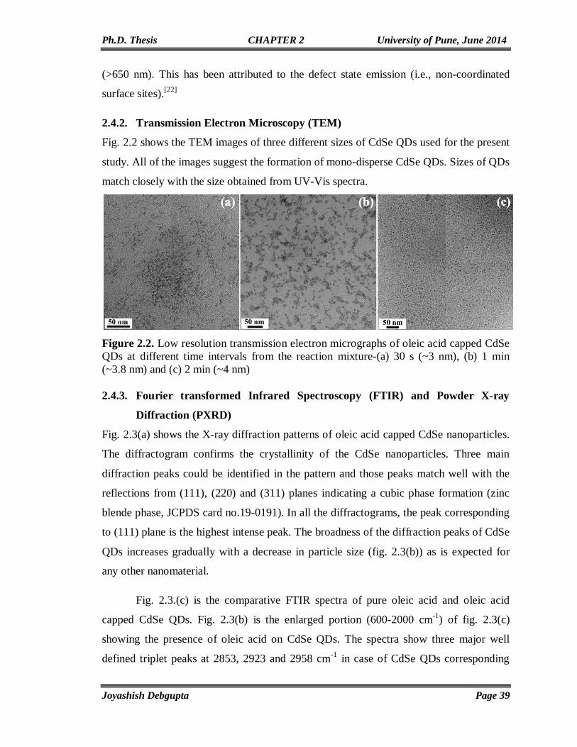
Ph.D. Thesis CHAPTER 2 University of Pune, June 2014
Joyashish Debgupta Page 39
(>650 nm). This has been attributed to the defect state emission (i.e., non-coordinated
surface sites).[22]
2.4.2. Transmission Electron Microscopy (TEM)
Fig. 2.2 shows the TEM images of three different sizes of CdSe QDs used for the present
study. All of the images suggest the formation of mono-disperse CdSe QDs. Sizes of QDs
match closely with the size obtained from UV-Vis spectra.
Figure 2.2. Low resolution transmission electron micrographs of oleic acid capped CdSe QDs at different time intervals from the reaction mixture-(a) 30 s (~3 nm), (b) 1 min (~3.8 nm) and (c) 2 min (~4 nm) 2.4.3. Fourier transformed Infrared Spectroscopy (FTIR) and Powder X-ray
Diffraction (PXRD)
Fig. 2.3(a) shows the X-ray diffraction patterns of oleic acid capped CdSe nanoparticles.
The diffractogram confirms the crystallinity of the CdSe nanoparticles. Three main
diffraction peaks could be identified in the pattern and those peaks match well with the
reflections from (111), (220) and (311) planes indicating a cubic phase formation (zinc
blende phase, JCPDS card no.19-0191). In all the diffractograms, the peak corresponding
to (111) plane is the highest intense peak. The broadness of the diffraction peaks of CdSe
QDs increases gradually with a decrease in particle size (fig. 2.3(b)) as is expected for
any other nanomaterial.
Fig. 2.3.(c) is the comparative FTIR spectra of pure oleic acid and oleic acid
capped CdSe QDs. Fig. 2.3(b) is the enlarged portion (600-2000 cm-1) of fig. 2.3(c)
showing the presence of oleic acid on CdSe QDs. The spectra show three major well
defined triplet peaks at 2853, 2923 and 2958 cm-1 in case of CdSe QDs corresponding
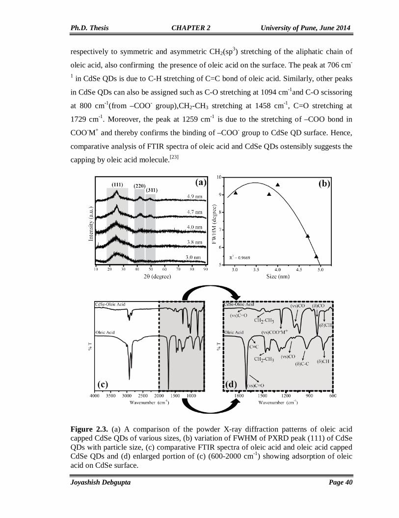
Ph.D. Thesis CHAPTER 2 University of Pune, June 2014
Joyashish Debgupta Page 40
respectively to symmetric and asymmetric CH2(sp3) stretching of the aliphatic chain of
oleic acid, also confirming the presence of oleic acid on the surface. The peak at 706 cm-
1 in CdSe QDs is due to C-H stretching of C=C bond of oleic acid. Similarly, other peaks
in CdSe QDs can also be assigned such as C-O stretching at 1094 cm-1and C-O scissoring
at 800 cm-1(from –COO- group),CH2-CH3 stretching at 1458 cm-1, C=O stretching at
1729 cm-1. Moreover, the peak at 1259 cm-1 is due to the stretching of –COO bond in
COO-M+ and thereby confirms the binding of –COO- group to CdSe QD surface. Hence,
comparative analysis of FTIR spectra of oleic acid and CdSe QDs ostensibly suggests the
capping by oleic acid molecule.[23]
Figure 2.3. (a) A comparison of the powder X-ray diffraction patterns of oleic acid capped CdSe QDs of various sizes, (b) variation of FWHM of PXRD peak (111) of CdSe QDs with particle size, (c) comparative FTIR spectra of oleic acid and oleic acid capped CdSe QDs and (d) enlarged portion of (c) (600-2000 cm-1) showing adsorption of oleic acid on CdSe surface.
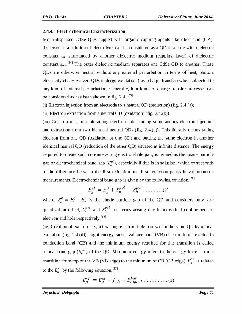
Ph.D. Thesis CHAPTER 2 University of Pune, June 2014
Joyashish Debgupta Page 41
2.4.4. Electrochemical Characterization
Mono-dispersed CdSe QDs capped with organic capping agents like oleic acid (OA),
dispersed in a solution of electrolyte, can be considered as a QD of a core with dielectric
constant εin surrounded by another dielectric medium (capping layer) of dielectric
constant εout.[24] The outer dielectric medium separates one CdSe QD to another. These
QDs are otherwise neutral without any external perturbation in terms of heat, photon,
electricity etc. However, QDs undergo excitation (i.e., charge transfer) when subjected to
any kind of external perturbation. Generally, four kinds of charge transfer processes can
be considered as has been shown in fig. 2.4. [25]
(i) Electron injection from an electrode to a neutral QD (reduction) (fig. 2.4.(a))
(ii) Electron extraction from a neutral QD (oxidation) (fig. 2.4.(b))
(iii) Creation of a non-interacting electron-hole pair by simultaneous electron injection
and extraction from two identical neutral QDs (fig. 2.4.(c)). This literally means taking
electron from one QD (oxidation of one QD) and putting the same electron in another
identical neutral QD (reduction of the other QD) situated at infinite distance. The energy
required to create such non-interacting electron-hole pair, is termed as the quasi- particle
gap or electrochemical band-gap (𝐸𝐸𝑔𝑔𝑒𝑒𝑒𝑒 ), especially if this is in solution, which corresponds
to the difference between the first oxidation and first reduction peaks in voltammetric
measurements. Electrochemical band-gap is given by the following equation,[26]
𝐸𝐸𝑔𝑔𝑒𝑒𝑒𝑒 = 𝐸𝐸𝑔𝑔0 + 𝛴𝛴𝑒𝑒𝑝𝑝𝑝𝑝𝑒𝑒 + 𝛴𝛴ℎ
𝑝𝑝𝑝𝑝𝑒𝑒 ………….(2)
where, 𝐸𝐸𝑔𝑔0 = 𝐸𝐸𝑒𝑒0 − 𝐸𝐸ℎ0 is the single particle gap of the QD and considers only size
quantization effect, 𝛴𝛴𝑒𝑒𝑝𝑝𝑝𝑝𝑒𝑒 and 𝛴𝛴ℎ
𝑝𝑝𝑝𝑝𝑒𝑒 are terms arising due to individual confinement of
electron and hole respectively.[15]
(iv) Creation of exciton, i.e., interacting electron-hole pair within the same QD by optical
excitation (fig. 2.4.(d)). Light energy causes valence band (VB) electron to get excited to
conduction band (CB) and the minimum energy required for this transition is called
optical band-gap (𝐸𝐸𝑔𝑔𝑝𝑝𝑝𝑝 ) of the QD. Minimum energy refers to the energy for electronic
transition from top of the VB (VB edge) to the minimum of CB (CB edge). 𝐸𝐸𝑔𝑔𝑝𝑝𝑝𝑝 is related
to the 𝐸𝐸𝑔𝑔𝑒𝑒𝑒𝑒 by the following equation,[27]
𝐸𝐸𝑔𝑔𝑝𝑝𝑝𝑝 = 𝐸𝐸𝑔𝑔𝑒𝑒𝑒𝑒 − 𝐽𝐽𝑒𝑒,ℎ − 𝐸𝐸𝑒𝑒𝑙𝑙𝑔𝑔𝑙𝑙𝑙𝑙𝑙𝑙𝑏𝑏𝑙𝑙𝑏𝑏 …………….(3)
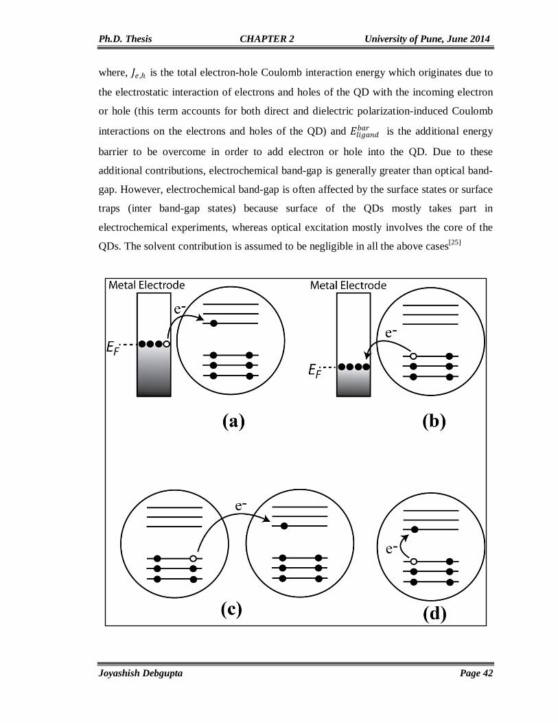
Ph.D. Thesis CHAPTER 2 University of Pune, June 2014
Joyashish Debgupta Page 42
where, 𝐽𝐽𝑒𝑒 ,ℎ is the total electron-hole Coulomb interaction energy which originates due to
the electrostatic interaction of electrons and holes of the QD with the incoming electron
or hole (this term accounts for both direct and dielectric polarization-induced Coulomb
interactions on the electrons and holes of the QD) and 𝐸𝐸𝑒𝑒𝑙𝑙𝑔𝑔𝑙𝑙𝑙𝑙𝑙𝑙𝑏𝑏𝑙𝑙𝑏𝑏 is the additional energy
barrier to be overcome in order to add electron or hole into the QD. Due to these
additional contributions, electrochemical band-gap is generally greater than optical band-
gap. However, electrochemical band-gap is often affected by the surface states or surface
traps (inter band-gap states) because surface of the QDs mostly takes part in
electrochemical experiments, whereas optical excitation mostly involves the core of the
QDs. The solvent contribution is assumed to be negligible in all the above cases[25]

Ph.D. Thesis CHAPTER 2 University of Pune, June 2014
Joyashish Debgupta Page 43
Figure 2.4. Different processes of charging QDs-(a) electron addition to a neutral QD, (b) electron removal from a QD, (c) creation of non-interacting electron-hole pair by mutual charge transfer and (d) optical excitation.[15], [25] 2.4.4.1. Differential Pulse Voltammetry (DPV) of oleic acid capped CdSe QDs
Differential pulse voltammetry is a very important voltammetric technique which
employs short, gradually increasing potential pulses for measurements. Current sampling
is done twice-one just before applying pulse and another just before ending the pulse. The
difference in the two currents is plotted against the applied potential. The y-axis in the
resultant voltammogram then becomes differential current rather than normal current
(which is generally used in normal voltammetry).[28] This effectively removes the
contribution due to background current (charging current) and so the peak obtained is
solely due to the redox process occurring in the system under study. Accordingly, fig. 2.5
shows a comparison of differential pulse voltammograms (DPVs) of five distinct sizes of
CdSe QDs in a typical non-aqueous electrolyte.
Figure 2.5. (a) Anodic and (b) Cathodic Differential pulse voltammograms of CdSe QDs capped by oleic acid; 0.2 cm diameter Pt-disk was used as working electrode, Pt wire as quasi reference and Counter electrodes; Scan rate was 10 mV/s and pulse amplitude was 50 mV; Dry dichloromethane was used for the study and TBAPF6 was used as supporting electrolyte; Dotted line shows the blank; in all cases concentration of QDs was kept in the µM (10-6 M) range.
The potential is swept cathodically from open circuit potential (OCP) to -1.5 V (fig.
2.5.(b)) and subsequently anodically from OCP to 1.5 V (fig. 2.5.(a)) with respect to a Pt
quasi-reference electrode. Each sample of CdSe QDs gives two distinct peaks – one
corresponds to reduction and the other corresponding to oxidation respectively. The

Ph.D. Thesis CHAPTER 2 University of Pune, June 2014
Joyashish Debgupta Page 44
HOMO and LUMO correspond to the first oxidation and first reduction peaks
respectively assuming one electron oxidation and reduction of CdSe QDs. The difference
between these two peaks thus represents the electrochemical bandgap (𝐸𝐸𝑔𝑔𝑒𝑒𝑒𝑒 ). Interestingly,
these two peaks shift towards each other systematically as we move from smaller to
larger sized particles as is expected due to quantum confinement effect (difference
between VB and CB decreases as the particle size increases). Absolute value of the band
(HOMO/LUMO) position is calculated according to the following equations:[29]
𝐸𝐸𝐻𝐻𝐻𝐻𝐻𝐻𝐻𝐻 = −𝐸𝐸[𝑝𝑝𝑜𝑜 𝑣𝑣𝑣𝑣 𝑁𝑁𝐻𝐻𝐸𝐸] + 4.75𝑒𝑒𝑒𝑒………………(4)
𝐸𝐸𝐿𝐿𝐿𝐿𝐻𝐻𝐻𝐻 = −𝐸𝐸[𝑏𝑏𝑒𝑒𝑙𝑙 𝑣𝑣𝑣𝑣 𝑁𝑁𝐻𝐻𝐸𝐸] + 4.75𝑒𝑒𝑒𝑒……………...(5)
where, 𝐸𝐸𝑝𝑝𝑜𝑜 and 𝐸𝐸𝑏𝑏𝑒𝑒𝑙𝑙 are the peak potentials for oxidation and reduction respectively and
4.75 eV is the absolute potential of normal hydrogen electrode (NHE).
There are also some interesting additional peaks observed in these
voltammograms. The extra oxidation peaks revealed for some particles before the
oxidation from the HOMO level can be attributed to the surface traps present at the mid-
gap region (as is revealed from photoluminescence). During potential sweep the traps
(either Cd or Se sites) get oxidized/reduced preferentially as compared to the HOMO
level. This is consistent with the literature and also supports the surface mediated electron
transfer as has been observed previously.[15] Table 2.1 represents absolute band positions
for each batch of the CdSe QDs. It also shows the values of optical bandgap for the
corresponding CdSe QD along with that of electrochemical HOMO-LUMO gap for
differently sized particles and a good correlation is observed between the two.
Interestingly, the bandgap value of particles changes as the particle size increases and
follows an inverse r2 (r = radius of the particle) relationship as has been predicted by Brus
for semiconductor nanoparticles.[30] However, in the present study, the electrochemical
HOMO-LUMO gap, obtained from DPV, is found to be less than the optical band-gap for
all the particles and this can be attributed to the presence of multiple surface traps in the
QDs as well as to the possible degradation of the QDs into Cd and Se upon multiple
electron transfer.[31] Presence of surface traps has already been confirmed from
photoluminescence (fig. 2.1(b)) (broad humps ranging between 650 and 800 nm). Solvent
contribution could also be significant in some cases.[32]

Ph.D. Thesis CHAPTER 2 University of Pune, June 2014
Joyashish Debgupta Page 45
Table 2.1.Band positions of CdSe QDs of different size
Particle size (nm)
HOMO (eV)
vs vacuum
LUMO (eV)
vs vacuum
Electrochemical Bandgap (𝑬𝑬𝒈𝒈𝒆𝒆𝒆𝒆) eV
Optical Bandgap (𝑬𝑬𝒈𝒈
𝒐𝒐𝒐𝒐) eV
3 -5.57 -3.23 2.34 2.39 3.8 -5.8 -3.72 2.08 2.26 4.0 -5.51 -3.33 2.18 2.23 4.7 -5.72 -3.5 2.22 2.12 4.9 -5.81 -3.57 2.24 2.09
Bulk -5.96 -4.08 1.8 1.74
Fig.2.6 shows the comparative band structures of different sized CdSe QDs
obtained by various groups.[15], [24], [33-35] The values obtained from this study matches
well with the theoretical values (Zunger[24] et al., sky blue diamonds in fig. 2.6.) as well
as experimental values from literature. However, a little divergence has been observed,
perhaps due to the effect of solvent (dichloromethane in our case).[32]
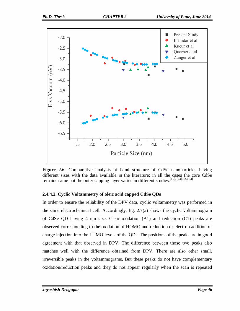
Ph.D. Thesis CHAPTER 2 University of Pune, June 2014
Joyashish Debgupta Page 46
Figure 2.6. Comparative analysis of band structure of CdSe nanoparticles having different sizes with the data available in the literature; in all the cases the core CdSe remains same but the outer capping layer varies in different studies.[15], [24], [33-34]
2.4.4.2. Cyclic Voltammetry of oleic acid capped CdSe QDs
In order to ensure the reliability of the DPV data, cyclic voltammetry was performed in
the same electrochemical cell. Accordingly, fig. 2.7(a) shows the cyclic voltammogram
of CdSe QD having 4 nm size. Clear oxidation (A1) and reduction (C1) peaks are
observed corresponding to the oxidation of HOMO and reduction or electron addition or
charge injection into the LUMO levels of the QDs. The positions of the peaks are in good
agreement with that observed in DPV. The difference between those two peaks also
matches well with the difference obtained from DPV. There are also other small,
irreversible peaks in the voltammograms. But these peaks do not have complementary
oxidation/reduction peaks and they do not appear regularly when the scan is repeated
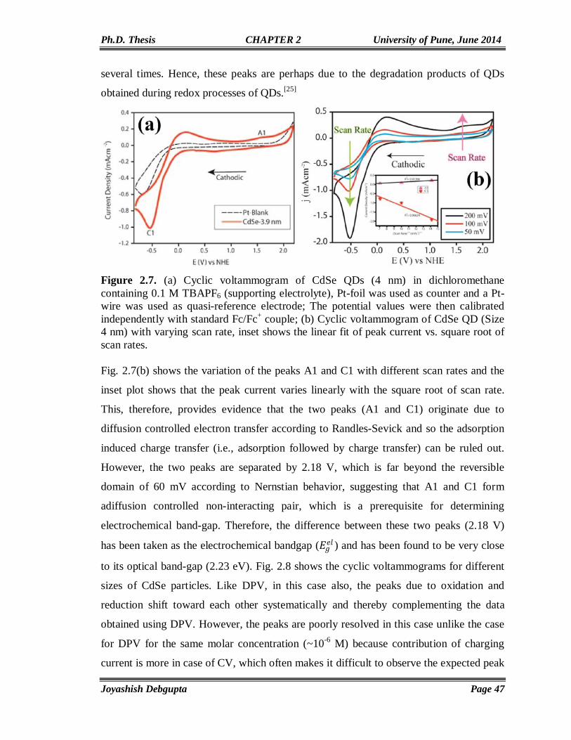
Ph.D. Thesis CHAPTER 2 University of Pune, June 2014
Joyashish Debgupta Page 47
several times. Hence, these peaks are perhaps due to the degradation products of QDs
obtained during redox processes of QDs.[25]
Figure 2.7. (a) Cyclic voltammogram of CdSe QDs (4 nm) in dichloromethane containing 0.1 M TBAPF6 (supporting electrolyte), Pt-foil was used as counter and a Pt-wire was used as quasi-reference electrode; The potential values were then calibrated independently with standard Fc/Fc+ couple; (b) Cyclic voltammogram of CdSe QD (Size 4 nm) with varying scan rate, inset shows the linear fit of peak current vs. square root of scan rates. Fig. 2.7(b) shows the variation of the peaks A1 and C1 with different scan rates and the
inset plot shows that the peak current varies linearly with the square root of scan rate.
This, therefore, provides evidence that the two peaks (A1 and C1) originate due to
diffusion controlled electron transfer according to Randles-Sevick and so the adsorption
induced charge transfer (i.e., adsorption followed by charge transfer) can be ruled out.
However, the two peaks are separated by 2.18 V, which is far beyond the reversible
domain of 60 mV according to Nernstian behavior, suggesting that A1 and C1 form
adiffusion controlled non-interacting pair, which is a prerequisite for determining
electrochemical band-gap. Therefore, the difference between these two peaks (2.18 V)
has been taken as the electrochemical bandgap (𝐸𝐸𝑔𝑔𝑒𝑒𝑒𝑒 ) and has been found to be very close
to its optical band-gap (2.23 eV). Fig. 2.8 shows the cyclic voltammograms for different
sizes of CdSe particles. Like DPV, in this case also, the peaks due to oxidation and
reduction shift toward each other systematically and thereby complementing the data
obtained using DPV. However, the peaks are poorly resolved in this case unlike the case
for DPV for the same molar concentration (~10-6 M) because contribution of charging
current is more in case of CV, which often makes it difficult to observe the expected peak

Ph.D. Thesis CHAPTER 2 University of Pune, June 2014
Joyashish Debgupta Page 48
over background. This, therefore, implies the advantage of DPV over CV for determining
band structure parameters.
Figure 2.8. Cyclic voltammograms of CdSe QDs of varying sizes in dichloromethane containing 0.1 M TBAPF6 as supporting electrolyte under identical condition. Concentrations are maintained in the micromolar range in order to compare DPV and CV. However, negligible variation in concentration is possible during experiment. Some peaks do not appear all the time and so they perhaps represent degradation of QDs upon electron transfer.[15]
2.4.4.3. Impedance measurements of the CdSe QDs solutions
Fig. 2.9(a) is the representative Nyquist plot of CdSe QD (3 nm) capped with oleic acid
in dichloromethane (CH2Cl2) on a pt-disk (0.2 cm diameter) working electrode at OCP
and at 1.75 V (vs NHE), i.e., at potential where oxidation of CdSe QD (3 nm) occurs
(HOMO oxidation). The impedance data (at OCP) has been divided into high frequency
where a depressed semicircle is observed and low frequency domain which shows a
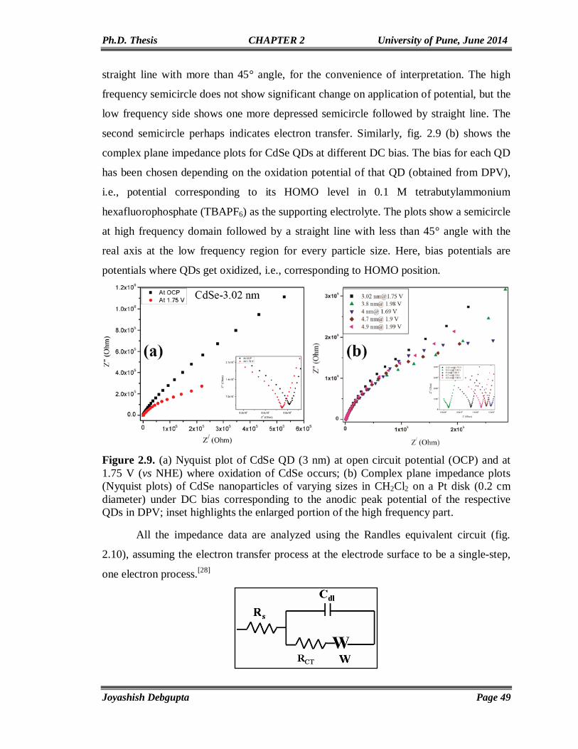
Ph.D. Thesis CHAPTER 2 University of Pune, June 2014
Joyashish Debgupta Page 49
straight line with more than 45° angle, for the convenience of interpretation. The high
frequency semicircle does not show significant change on application of potential, but the
low frequency side shows one more depressed semicircle followed by straight line. The
second semicircle perhaps indicates electron transfer. Similarly, fig. 2.9 (b) shows the
complex plane impedance plots for CdSe QDs at different DC bias. The bias for each QD
has been chosen depending on the oxidation potential of that QD (obtained from DPV),
i.e., potential corresponding to its HOMO level in 0.1 M tetrabutylammonium
hexafluorophosphate (TBAPF6) as the supporting electrolyte. The plots show a semicircle
at high frequency domain followed by a straight line with less than 45° angle with the
real axis at the low frequency region for every particle size. Here, bias potentials are
potentials where QDs get oxidized, i.e., corresponding to HOMO position.
Figure 2.9. (a) Nyquist plot of CdSe QD (3 nm) at open circuit potential (OCP) and at 1.75 V (vs NHE) where oxidation of CdSe occurs; (b) Complex plane impedance plots (Nyquist plots) of CdSe nanoparticles of varying sizes in CH2Cl2 on a Pt disk (0.2 cm diameter) under DC bias corresponding to the anodic peak potential of the respective QDs in DPV; inset highlights the enlarged portion of the high frequency part.
All the impedance data are analyzed using the Randles equivalent circuit (fig.
2.10), assuming the electron transfer process at the electrode surface to be a single-step,
one electron process.[28]
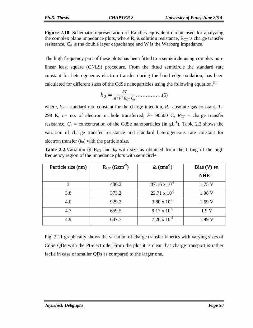
Ph.D. Thesis CHAPTER 2 University of Pune, June 2014
Joyashish Debgupta Page 50
Figure 2.10. Schematic representation of Randles equivalent circuit used for analyzing the complex plane impedance plots, where Rs is solution resistance, RCT is charge transfer resistance, Cdl is the double layer capacitance and W is the Warburg impedance.
The high frequency part of these plots has been fitted to a semicircle using complex non-
linear least square (CNLS) procedure. From the fitted semicircle the standard rate
constant for heterogeneous electron transfer during the band edge oxidation, has been
calculated for different sizes of the CdSe nanoparticles using the following equation.[28]
𝑘𝑘0 = 𝑅𝑅𝑅𝑅𝑙𝑙2𝐹𝐹2𝑅𝑅𝐶𝐶𝑅𝑅 𝐶𝐶𝑙𝑙
…………….(6)
where, k0 = standard rate constant for the charge injection, R= absolute gas constant, T=
298 K, n= no. of electron or hole transferred, F= 96500 C, RCT = charge transfer
resistance, Cn = concentration of the CdSe nanoparticles (in gL-1). Table 2.2 shows the
variation of charge transfer resistance and standard heterogeneous rate constant for
electron transfer (k0) with the particle size.
Table 2.2.Variation of RCT and k0 with size as obtained from the fitting of the high frequency region of the impedance plots with semicircle
Particle size (nm) RCT (Ωcm-2) k0 (cms-1) Bias (V) vs. NHE
3 486.2 87.16 x 10⁻⁵ 1.75 V
3.8 373.2 22.71 x 10⁻⁵ 1.98 V
4.0 929.2 3.80 x 10⁻⁵ 1.69 V
4.7 659.5 9.17 x 10⁻⁵ 1.9 V
4.9 647.7 7.26 x 10⁻⁵ 1.99 V
Fig. 2.11 graphically shows the variation of charge transfer kinetics with varying sizes of
CdSe QDs with the Pt-electrode. From the plot it is clear that charge transport is rather
facile in case of smaller QDs as compared to the larger one.

Ph.D. Thesis CHAPTER 2 University of Pune, June 2014
Joyashish Debgupta Page 51
Figure 2.11. (a) Particle size vs heterogeneous electron transfer rate constants obtained from impedance measurements, it follows apparently an exponential decay with increment in particle size.
The size dependency can be explained using Marcus’s theory for nonadiabatic
electron transfer in the classical activation limit.[35-36] Theoretical calculation gives the
following equation for rate constant for any electrochemical reaction,
𝑘𝑘 = 𝐾𝐾𝑃𝑃 ,𝐻𝐻𝜈𝜈𝑙𝑙𝜅𝜅𝑒𝑒𝑒𝑒 exp−𝛥𝛥𝐺𝐺≠
𝑅𝑅𝑅𝑅 … … … … … … … … … . (7)
where, 𝛥𝛥𝐺𝐺≠is the activation energy for oxidation/reduction, KP,O is a precursor
equilibrium constant, νn is the nuclear frequency factor (s-1) and κel is the electronic
transmission coefficient which is related to the tunneling probability of electron.
According to Marcus theory, 𝛥𝛥𝐺𝐺≠ is given by,
𝛥𝛥𝐺𝐺≠ = 𝜆𝜆4
(1 + 𝐹𝐹(𝐸𝐸−𝐸𝐸0)𝜆𝜆
)2………………………(8)
where, E and E0 are the formal and standard redox potentials respectively for the redox
process, F is the Faraday constant and λ is the reorganization energy. It is clear from the
above equations (7 & 8) that k has an inverse exponential relationship with activation
enrgy or applied potential in particular (driving force).
In the present case, the driving force for electron transfer between Pt-electrode and
CdSe QD has been taken as the formal redox potential of the QDs of varying size. As is
seen from the previous section that the potential for oxidation increases with the increase
in particle size (fig. 2.9(b)). Driving force thus increases proportionally with increase in
Ph.D. Thesis CHAPTER 2 University of Pune, June 2014
Joyashish Debgupta Page 52
QD size as per equation 8. Hence, the electron transfer rate increases with decrease in
particle size.
The size dependent electron transfer rate can also be explained by considering their size
dependent diffusion coefficient. The variation of heterogeneous electron transfer rate
constant against particle size interestingly gives an exponential decay behavior, which
coincides with the Brus correlation. The fact that the charge transfer kinetics is rather fast
for small size particles, is in line with the fact that smaller size particle diffuses faster
than the larger ones due to less visco-elastic drag in the same medium and hence the rate
of electron transfer is also higher. We have used the Modified Stokes-Einstein equation
(eqn.8)[37] to calculate the hydrodynamic radii of different size QDs in dichloromethane
as summarized in Table 2.3.
𝐷𝐷 = 𝑘𝑘𝑅𝑅6𝜋𝜋𝜋𝜋𝑏𝑏
……………..(9)
where, D is the diffusion coefficient, k is the Boltzmann const., η is viscosity and r is the
hydrodynamic diameter of the particles (taken as the sum of nanocrystal diameter and
twice the length of oleic acid chain length (1.97 nm). The values obtained are very much
similar to that obtained previously for CdTe nanoparticles.[16]
However, the role of surface state, effect of migration of the QDs upon charge
transfer, electrical as well as electrochemical nature of the capping molecules (here oleic
acid), effect of specific adsorption of ions (from supporting electrolyte), reorganization of
surface dipoles etc. are neglected while explaining the trend in heterogeneous electron
transfer kinetics of these QDs. But all the above parameters are important for the proper
understanding of the electron transfer rate in QDs.
Table 2.3.Diffusion coefficient calculated from Stokes-Einstein theory (viscosity of the dichloromethane is taken as 0.393 cP)
Particle size/Core
diameter (nm)
(From UV-VIS)
Hydrodynamic
Diameter
(nm)
Diffusion Coeff.
(cm.s-1)
3 6.96 2.43 x 10⁻⁶
3.8 7.74 2.18 x 10⁻⁶
4 7.94 2.13 x 10⁻⁶

Ph.D. Thesis CHAPTER 2 University of Pune, June 2014
Joyashish Debgupta Page 53
4.7 8.64 1.96 x 10⁻⁶
4.9 8.84 1.91 x 10⁻⁶
It is, therefore, observed from all the above discussions that band structure
parameters can be easily obtained using electrochemistry such as differential pulse
voltammetry or cyclic voltammetry, but of course, with some limitations. In particular,
DPV gives more reliable information when the concentration of the QDs is too low to get
appreciable signal over the background. Again, as the capacitance increases with
decrease in particle size (according to the Concentric Sphere Capacitance Model), cyclic
voltammetry becomes less effective in resolving the redox peaks over the background
charging current. DPV, thus, becomes extremely useful to distinguish and identify the
redox peaks over the background, because it uses differential currents before and after the
application of voltage pulse. Moreover, electrochemical impedance technique provides
valuable information about the kinetics of charge transfer often inextricable by fitting the
experimental data using suitable equivalent circuit despite its model-dependence. A
rough estimate of the thermodynamic information (free energy change for example) is
possible for CdSe QDs of varying size. For instance, our preliminary data unambiguously
suggest that the change in free energy decreases as the particle size increases especially
below a critical threshold. All the above studies suggest a systematic trend in charge
transfer kinetics for different size QDs illustrating that smaller sized QDs react faster
than the larger ones arising perhaps from fact that the rate of diffusion is faster in case of
smaller QDs assuming same solvation parameters.
2.5. Conclusion
We have synthesized five different sizes of oleic acid capped CdSe QDs (sizes below 5
nm, i.e., below the excitonic Bohr radius of CdSe QDs) and have investigated their
electron transfer kinetics using various optical and electrochemical methods. The DPV of
oleic acid capped CdSe QDs reveals a band gap that varies with the particle size, despite
being reasonably close to the corresponding optical band gap value. The possibility of
existence of surface traps, which might interfere with the voltammetric measurements,
cannot be ignored. Thus, DPV has been found to be a very useful technique in
Ph.D. Thesis CHAPTER 2 University of Pune, June 2014
Joyashish Debgupta Page 54
determining band structure parameters (such HOMO-LUMO gap of the QDs especially at
very low concentrations to 0.1 µM) assuming negligible solvation effects. Cyclic
voltammetry has also been carried out to supplement the DPV outcome and the results
obtained are in excellent agreement to the DPV observations. Moreover, electrochemical
impedance analysis of the CdSe QD solutions shows that the kinetics of charge transfer to
or from the particles from or to the electrode becomes more facile with the decrease in
core diameter of the particles, which indeed manifests varying diffusion coefficients of
the differently sized particles. In fact, the smallest particles (3.nm) can transfer charge
~12 times faster than that of the largest particles (4.9 nm) although the diffusion
coefficient for the smallest particles varies only ~1.2 times than that for largest particles.
All methods are experimentally simple and do not require complicated instrumental infra-
structure or complex hardware However, the charge transfer kinetics is also likely to be
influenced by several other factors including the surrounding dielectric medium (solvent,
supporting electrolyte etc.) and many of these are not considered in this study. Almost
identical conditions have been maintained during the experiments to avoid complications
arising from such factors and we hope these results would be useful to understand the
mechanism of charge transfer of QDs.
2.6. References
1. Michalet, X.; Pinaud, F.; Lacoste, T. D.; Dahan, M.; Bruchez, M.P.; Alvisatos, A.P.;
Weiss, S. Single Mol.2001, 2 (4), 261.
2. Bakalova, R.; Ohba, H.; Zhelev, Z.; Nagase, T.; Jose, R.; Ishikawa, M.; Baba, Y.
Nano Lett. 2004, 4 (9), 1567.
3. Schlamp, M.C.; Peng, X.; Alvisatos, A.P. J. Appl. Phys.1997, 82 (11), 5837.
4. Klimov, V. I.; Mikhailovsky, A. A.; Xu, S.; Malko, A.; Hollingsworth, J. A.;
Leatherdale, C. A.; Eisler, H. J.; Bawendi, M.G. Science 2000, 290 (5490), 314.
5. Murray, C.B.; Kagan, C.R.; Bawendi, M.G. Annu. Rev. Mater. Sci. 2000, 30 (1), 545.
6. Qu, L.; Peng, Z. A.; Peng, X. Nano Lett. 2001, 1 (6), 333.
7. Brus, L. J. Phys. Chem.1986, 90 (12), 2555.
8. Alvisatos, A.P. Science 1996, 271, 933.
9. Bouroushian, M.: Electrochemistry of metal chalcogenides; Springer, 2010.
Ph.D. Thesis CHAPTER 2 University of Pune, June 2014
Joyashish Debgupta Page 55
10. Ingram, R. S.; Hostetler, M. J.; Murray, R.W.; Schaaff, T. G.; Khoury, J. T.; Whetten,
R. L.; Bigioni, T. P.; Guthrie, D. K.; First, P. N. J. Am. Chem. Soc. 1997, 119, 9279.
11. Chen, S.; Murray, R.W.; Feldberg, S.W. J. Phys. Chem. B 1998, 102, 9898.
12. Chen, S.; Ingram, R. S.; Hostetler, M. J.; Pietron, J. J.; Murray, R.W.; Schaaff, T. G.;
Khoury, J.T.; Alvarez, M.M.; Whetten, R. L. Science 1998, 280, 2098.
13. Templeton, A. C.; Wuelfing, W. P.; Murray, R.W. Acc. Chem. Res. 2000, 33, 27.
14. Ding, Z.; Quinn, B. M.; Haram, S. K.; Pell, L. F.; Korgel, B. A.; Bard, A. J. Science
2002, 296, 1293.
15. Haram, S. K.; Quinn, B. M.; Bard, A. J. J. Am. Chem. Soc. 2001, 123, 8860.
16. Inamdar, S. N.; Ingole, P. P.; Haram, S. K. Chem. Phys. Chem. 2008, 9, 2574.
17. Bae, Y.; Myung, N.; Bard, A.J. Nano Lett. 2004, 4, 1153.
18. Motl, N. E.; Ewusiannan, E.; Sines, I.T.; Jensen, L.; Schaak, R. E. J. Phy. Chem. C
2010, 114, 19263.
19. Reimann, S. M.; Manninen, M. Rev. of Mod. Phys. 2002, 74, 1283.
20. Sapra, S.; Shanthi, N.; Sarma, D. D. Phys. Rev. B 2002, 66, 205202.
21. Yu, W. W.; Qu, L.; Guo, W.; Peng, X. Chem. Mater. 2003, 15, 2854.
22. Murray, C. B.; Norris, D. J.; Bawendi, M. G. J. Am. Chem. Soc. 1993, 115, 8706.
23. Qu, L.; Yu, W. W.; Peng, X.; Nano Lett. 2004, 4, 465–469.
24. (a) Hamizi, N. A.; Johan, M. R. Mater. Chem. Phys. 2010, 124, 395. (b) Silverstein,
R. M.; Webster, F. X.; Kiemle, D. J., Spectrometric Identification of Organic
Compounds, 7th Ed., John Wiley & Sons.
25. Franceschetti, A.; Zunger, A. Phys. Rev. B 2000, 62, 2614.
26. Amelia, M.; Lincheneau, C.; Silvi, S.; Credi, A.: Electrochemical properties of CdSe
and CdTe quantum dots. Chem. Soc. Rev. 2012, 41, 5728.
27. (a) Jasieniak, J.; Califano, M.; Watkins, S. E. ACS nano 2011, 5, 5888. (b) Liu, J.;
Yang, W.; Li, Y.; Fan, L.; Li, Y. Phys. Chem. Chem. Phys. 2014, 16, 4778.
28. Bard, A. J.; Faulkner, L. R. Electrochemical Methods, Fundamentals and
Applications; 2nd ed. John Wiley & Sons: New York, 2001.
29. Cardona, C. M.; Li, W.; Kaifer, A. E.; Stockdale, D.; Bazan, G. C. Adv. Mater. 2011,
23, 2367.
30. Bawendi, M.G.; Steigerwald, M.L.; Brus, L. E. Annu. Rev. Phys. Chem.1990, 41, 477.

Ph.D. Thesis CHAPTER 2 University of Pune, June 2014
Joyashish Debgupta Page 56
31. (a) Impellizzeri, S.; Monaco, S.; Yildiz, I.; Amelia, M.; Credi, A.; Raymo, F. M. J.
Phys. Chem. C 2010, 114 (15), 7007. (b) Amelia, M.; Impellizzeri, S.; Monaco, S.;
Yildiz, I.; Silvi, S.; Raymo, F. M.; Credi, A. Chem. Phys. Chem. 2011, 12 (12), 2280.
32. Kucur, E.; Bücking, W.; Giernoth, R.; Nann, T. J. Phys. Chem. B 2005, 109, 20355.
33. Querner, C.; Reiss, P.; Sadki, S.; Zagorska, M.; Pron, A. Phys. Chem. Chem. Phys.
2005, 7, 3204.
34. Leatherdale, C. A.; Bawendi, M. G. Phys. Rev. B 2001, 63 (16), 1653151.
35. Marcus, R. A. J. Chem. Phys. 1965, 43, 679.
36. (a) Sutin, N. Prog. Inorg. Chem. 1983, 30, 441. (b) Bhat, M. A. New J. Chem. 2009,
33 (1), 207.
37. (a) Edward, J. T. J. Chem. Educ.1970, 47, 261. (b) Zwanzig, R.; Harrison, A. K. J.
Chem. Phys.1985, 83, 5861.
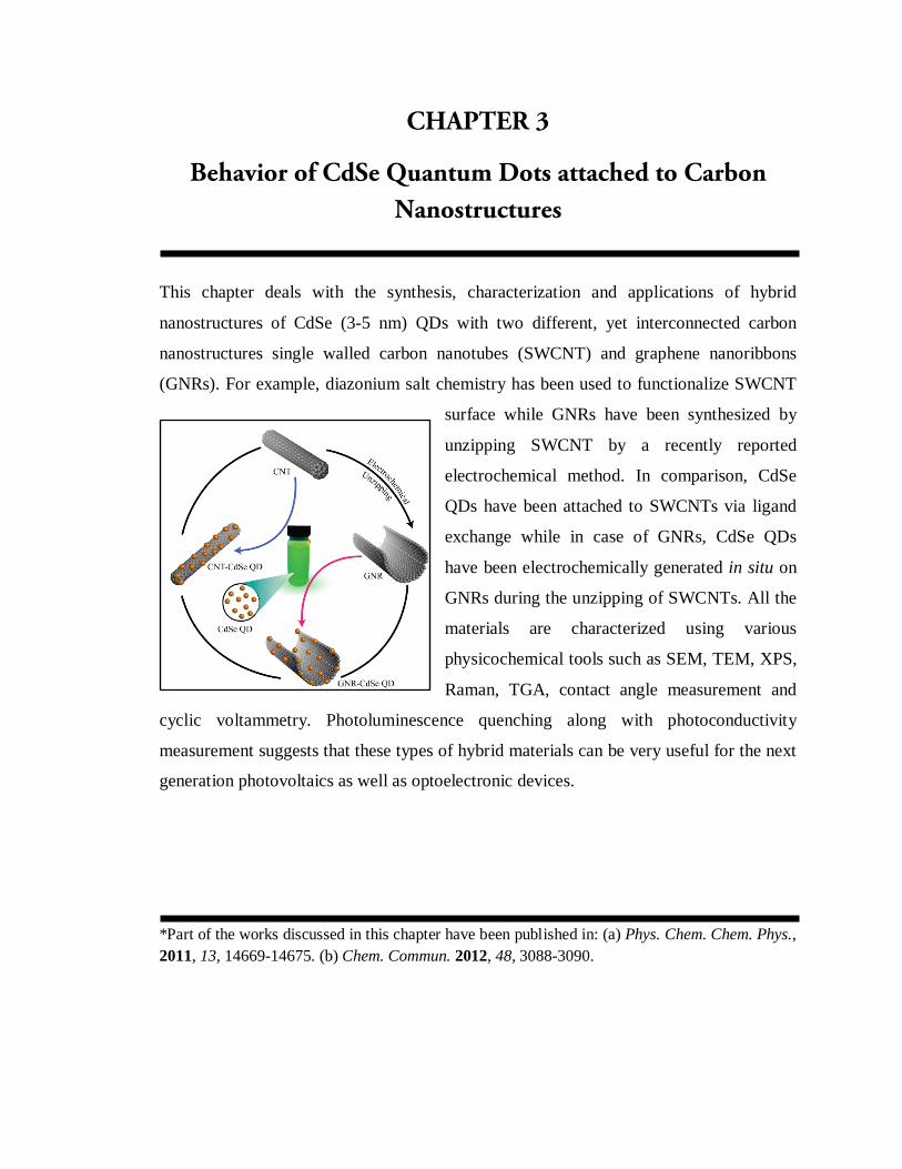
CHAPTER 3
Behavior of CdSe Quantum Dots attached to Carbon Nanostructures
This chapter deals with the synthesis, characterization and applications of hybrid
nanostructures of CdSe (3-5 nm) QDs with two different, yet interconnected carbon
nanostructures single walled carbon nanotubes (SWCNT) and graphene nanoribbons
(GNRs). For example, diazonium salt chemistry has been used to functionalize SWCNT
surface while GNRs have been synthesized by
unzipping SWCNT by a recently reported
electrochemical method. In comparison, CdSe
QDs have been attached to SWCNTs via ligand
exchange while in case of GNRs, CdSe QDs
have been electrochemically generated in situ on
GNRs during the unzipping of SWCNTs. All the
materials are characterized using various
physicochemical tools such as SEM, TEM, XPS,
Raman, TGA, contact angle measurement and
cyclic voltammetry. Photoluminescence quenching along with photoconductivity
measurement suggests that these types of hybrid materials can be very useful for the next
generation photovoltaics as well as optoelectronic devices.
*Part of the works discussed in this chapter have been published in: (a) Phys. Chem. Chem. Phys., 2011, 13, 14669-14675. (b) Chem. Commun. 2012, 48, 3088-3090.
Ph.D. Thesis CHAPTER 3 University of Pune, June 2014
Joyashish Debgupta Page 58
3.1. Introduction
Semiconductor quantum dots (QDs), often termed as the giant artificial atoms, of varying
size and shape possess unique properties like tunable absorption of light,[1] and
generation of multiple excitons[2] which make them ideal candidate for solar cells and
other optoelectronic devices. Consequentially, the exploration of the structure and
properties of these QDs has strong implications on the development of high throughput
optoelectronic devices.[3]Moreover, carbon-based materials such as diamond, carbon
nanotubes (CNTs), carbon nanofibers (CNFs), carbon nanospheres (CNSs) and graphenes
coupled with QDs are more favorable in terms of their better stability and mechanical
strength.[4] Among these, CNTs and graphene do possess unique structural, electronic,
mechanical and optical properties and hence they are actively sought as an effective
component of a variety of devices including field-effect transistors (FETs), Li-ion
batteries, light-emitting diodes (LEDs) and also as a catalyst support in fuel cells.[5]
Additionally, higher surface area, mechanical strength and thermal stability of these
materials suggest a host of wide-ranging, potential applications in heterogeneous
catalysis, field emitters, high-strength engineering fibers, sensors, actuators, composites,
tips for scanning probe microscopy, gas storage media and next generation molecular and
electronic devices.[6] Blending of these two different materials, therefore, can give rise to
important hybrid materials with improved characteristics than that of the individual
materials.
However, several challenges lie ahead in finding suitable methods for
successfully combining these two materials. For example, although there are several
strategies for attaching CdSe QDs to different carbon nanostructures, a few have serious
stability issues, Some of them rely on covalent functionalization of carbon nanostructures
followed by chemical binding of QDs by means of suitable chemical reactions, or
polymer wrapping of carbon structures for attachment of QDs or in situ synthesis. But
almost all the methods suffer from common limitations of using high temperature,
multistep reactions, low yield and size control of the QDs and above all difficulties of
obtaining a uniform distribution of QDs on the carbon surface. Moreover, detailed
characterization studies on the performance of such hybrids are rare.

Ph.D. Thesis CHAPTER 3 University of Pune, June 2014
Joyashish Debgupta Page 59
In the previous chapter, we have discussed the hot injection synthesis of CdSe
QDs of varying size and shape with possible mono-dispersed size distribution. It has also
been demonstrated that their electronic properties/band structure parameters are very
much dependent on their size and shape. But nothing has been discussed about their
properties in presence of carbon nanostructures.
Present chapter, therefore, aims to develop a new simple methodology for
synthesizing CdSe QD-carbon nanostructure hybrids in order to explore their properties
and possible applications. Two different nanostructures of carbon, namely single walled
carbon nanotubes (SWCNTs) and graphene nanoribbons (GNRs) have been chosen for
the study mainly due to their topological relationship. GNRs have been synthesized by
electrochemical unzipping of SWCNTs and CdSe QDs are generated on GNRs by means
of in situ electro-deposition.[7] SWCNTs have been functionalized with diazonium salt of
4-aminothiophenol (4-ATP) to obtain –SH terminated SWCNTs and then oleic acid
capped CdSe QDs have been exchanged with –SH group to get CdSe QD decorated
SWCNT. The hybrids have been characterized with many techniques including SEM,
EDAX, TEM, Raman, UV-Vis, Photoluminescence, Cyclic voltammetry,
Thermogravimetry and Contact angle measurements.
3.2. Experimental Section
3.2.1. Materials
CNTs were obtained from Carbon Nanotechnologies Inc. and were purified according to
the reported protocol.[7]Sodium dodecylsulphonate (SDS), and 4-aminothiophenol were
purchased from Aldrich and used as received. H2SO4 (98%), HCl (38%), NaNO2, H2O2
were received from Thomas Baker and used without any further purification. PTFE filter
paper was obtained from Rankem. MilliQ water (DI water) was used for all purposes
unless otherwise stated. Cadmium oxide (CdO), trioctyl phosphine (TOP) and 1-
octadecene were purchased from Aldrich and used as received. Se powder, hexane and
ethanol (99.9%) of analytical reagent grade were purchased from Thomas Baker. Oleic
acid was purchased from Rankem and used without further purification. Acetonitrile
(CH3CN, HPLC grade) and Dichloromethane (CH2Cl2. AR grade) were purchased from
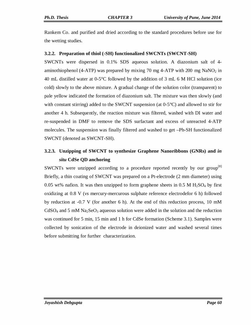
Ph.D. Thesis CHAPTER 3 University of Pune, June 2014
Joyashish Debgupta Page 60
Rankem Co. and purified and dried according to the standard procedures before use for
the wetting studies.
3.2.2. Preparation of thiol (-SH) functionalized SWCNTs (SWCNT-SH)
SWCNTs were dispersed in 0.1% SDS aqueous solution. A diazonium salt of 4-
aminothiophenol (4-ATP) was prepared by mixing 70 mg 4-ATP with 200 mg NaNO2 in
40 mL distilled water at 0-5°C followed by the addition of 3 mL 6 M HCl solution (ice
cold) slowly to the above mixture. A gradual change of the solution color (transparent) to
pale yellow indicated the formation of diazonium salt. The mixture was then slowly (and
with constant stirring) added to the SWCNT suspension (at 0-5°C) and allowed to stir for
another 4 h. Subsequently, the reaction mixture was filtered, washed with DI water and
re-suspended in DMF to remove the SDS surfactant and excess of unreacted 4-ATP
molecules. The suspension was finally filtered and washed to get –Ph-SH functionalized
SWCNT (denoted as SWCNT-SH).
3.2.3. Unzipping of SWCNT to synthesize Graphene Nanoribbons (GNRs) and in
situ CdSe QD anchoring
SWCNTs were unzipped according to a procedure reported recently by our group[8]
Briefly, a thin coating of SWCNT was prepared on a Pt-electrode (2 mm diameter) using
0.05 wt% nafion. It was then unzipped to form graphene sheets in 0.5 M H2SO4 by first
oxidizing at 0.8 V (vs mercury-mercurous sulphate reference electrodefor 6 h) followed
by reduction at -0.7 V (for another 6 h). At the end of this reduction process, 10 mM
CdSO4 and 5 mM Na2SeO3 aqueous solution were added in the solution and the reduction
was continued for 5 min, 15 min and 1 h for CdSe formation (Scheme 3.1). Samples were
collected by sonication of the electrode in deionized water and washed several times
before submitting for further characterization.

Ph.D. Thesis CHAPTER 3 University of Pune, June 2014
Joyashish Debgupta Page 61
Scheme 3.1. Electrochemical unzipping of SWCNT and subsequent CdSe nanoparticle decoration on the so formed GNRs; pristine SWCNT coated on Pt foil is electrochemically unzipped in 0.5 M H2SO4 at room temperature; CdSe has been subsequently deposited on GNRs using CdSO4 and Na2SeO3 as Cd and Se precursors respectively during the reduction of oxidized GNRs. 3.2.4. Exchange of oleic acid capped CdSe QDs with SWCNT-SH
18 mg of CdO was taken in a four-neck RB flask along with 0.6 ml oleic acid and 10 ml
1-octadecene (ODE). A Se-precursor (Se-TOP) solution was prepared by dissolving 32
mg Se powder in 5 ml ODE containing 0.6 mL trioctylphosphine (TOP) by slight
warming at 60°C. The RB flask containing CdO was then heated at 190°C when red CdO
dissolved completely to give a colorless solution (Cd-oleate). The heating was continued
until it reached to 230°C, when 1 ml Se-TOP was quickly injected into the reaction
mixture when the solution turned light yellow due to the formation of very small CdSe
NPs. The heating was subsequently stopped and the particles were allowed to settle at
that temperature. Aliquotes were collected at different time interval (30 s, 1 min, 3 min)
to get different particle sizes. The nanoparticles (NPs) were then precipitated out from the
solution by using a small amount of hexane followed by copious amount of ethanol. This
was then centrifuged and washed and the procedure was repeated 5-6 times to get pure
nanocrystals. The precipitate was then vacuum dried to obtain dry powder of CdSe
nanoparticles.Oleic acid capped CdSe NPs (CdSe-OA) (concentration of CdSe
suspension was maintained by fixing the first excitonic peak intensity at 0.1 optical

Ph.D. Thesis CHAPTER 3 University of Pune, June 2014
Joyashish Debgupta Page 62
density throughout all our experiments) were then exchanged by mixing the DMF
suspension of SWCNT-SH (12.7 mg ml-1) with toluene soluble CdSe-OA.
3.2.5. Ozonolysis of MWCNTs
Multiwalled carbon nanotubes (MWCNTs) were prepared by a CVD method[9] using a
ferrocene and xylene mixture at 700°C in a tubular furnace in Ar-flow. Ozonolized bucky
papers for this study were prepared as described elsewhere.[10] In brief, MWCNTs (purity
>90 %,diameter 20-30 nm and ~1% contains CNTs having diameter 100-150 nm as
determined from TEM analysis; not shown), dispersed in dichloromethane (60 mg in 40
mL CH2Cl2), were subjected to ozonolysis in a suitable reactor (Fischer Ltd.) for about an
hour, quenched with dimethyl sulphide(2 mL),washed with dichloromethane and
subsequently filtered and dried at 800 C under vacuum (this ozonized sample is denoted
as oz-MWCNT while pristine sample is described as p-MWCNT). Finally, the dried
material was pressed at 0.2 bar pressure to obtain bucky paper (60-80 µm thick).
3.3. Structural and Morphological Characterization
3.3.1. Scanning electron microscopy (SEM) and EDAX
The surface morphology of the samples was examined by using a Quanta 200 3D, FEI
scanning electron microscope (SEM) operating at 30 kV.A small piece of FTO plate
containing the sample was mounted on aluminium stubs and micrographs were recorded
with a 30 kV tension and 20 pA current with the help of a camera attached on the high
resolution recording unit. This SEM instrument was equipped with Phoenix energy
dispersive spectral (EDS) analysis setup for the elemental analysis.
3.3.2. Thermogravimetric analysis (TGA)
Thermogravimetric analysis was carried out on a TGA Q5000 TA Instruments - Thermal
analyzer from 50°C to 900°C at a rate of 10°C/ min in air as well as in nitrogen. Both p-
MWCNT and oz-MWCNTs were soaked in dichloromethane and acetonitrile for 2 h
prior to TGA measurements.
3.3.3. XPS analysis
X-ray photoelectron spectroscopic (XPS) measurements were carried out on a VG Micro
Tech ESCA 3000 instrument at a pressure of > 1x10⁻⁹Torr (pass energy of 50 eV with an
electron take off angle 60o and an overall resolution of 1 eV) using Mg Kα (source, hν =

Ph.D. Thesis CHAPTER 3 University of Pune, June 2014
Joyashish Debgupta Page 63
1253.6 eV) radiation. The alignment of binding energy (BE) was calibrated using Au 4f
binding energy of 84 eV as the reference. The X-ray flux (power 70 W) was kept
deliberately low in order to reduce the beam-induced damage. The spectra were fitted
using a combined polynomial and Shirley type background function.[11]
3.3.4. Micro Raman
All Raman spectroscopy measurements were carried out at room temperature on an HR
800 Raman spectrophotometer (Jobin Yvon HORIBA, France) using monochromatic
radiation emitted by a He−Ne laser (632.8nm), operating at 20 mW. The experiment was
repeated several times to verify the consistency of the spectra.
3.3.5. Contact angle measurement
All contact angle measurements were performed by a sessile drop method on a GBX
model (DIGIDROP contact angle instrument) using Windrop software. In case of
MWCNTs and oz-MWCNTs, contact angle measurements were performed after fixing
the bucky paper (thickness 0.5 mm) on a cleaned, dry glass slide with double side stick-
tape with no effect due to the tape. Extreme care has been taken in carrying out these
measurements to monitor contact angle values within 1-2 minutes to avoid the
evaporation effects. All contact angle measurements were carried out at room
temperature (27oC) and constant humidity (40-50%) with a standard deviation of ± 2o.
3.3.6. Electrical Characterizations
Photoconductivity of the sample was measured by two probe method using KEITHLEY
source metre and voltmeter in presence of 1.5 AM light source.
3.4. Results and Discussion
3.4.1. FTIR analysis
FTIR is very valuable technique to know the functional groups present on CNTs both
before and after chemical modification. It also gives information about the possibility of
functional groups being generated during electrochemical unzipping of CNTs.
Accordingly, Fig. 3.1(a) and (b) display a superimposition of the representative FTIR
spectra of p-SWCNT and un-SWCNT-CdSe composite showing interesting structural
changes on SWCNT surface due to electrochemical oxidation. The peak originating at
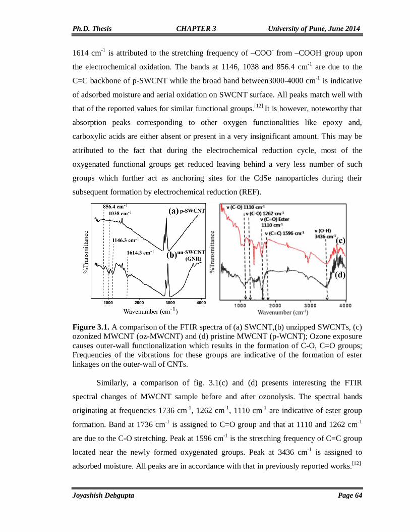
Ph.D. Thesis CHAPTER 3 University of Pune, June 2014
Joyashish Debgupta Page 64
1614 cm-1 is attributed to the stretching frequency of –COO- from –COOH group upon
the electrochemical oxidation. The bands at 1146, 1038 and 856.4 cm-1 are due to the
C=C backbone of p-SWCNT while the broad band between3000-4000 cm-1 is indicative
of adsorbed moisture and aerial oxidation on SWCNT surface. All peaks match well with
that of the reported values for similar functional groups.[12] It is however, noteworthy that
absorption peaks corresponding to other oxygen functionalities like epoxy and,
carboxylic acids are either absent or present in a very insignificant amount. This may be
attributed to the fact that during the electrochemical reduction cycle, most of the
oxygenated functional groups get reduced leaving behind a very less number of such
groups which further act as anchoring sites for the CdSe nanoparticles during their
subsequent formation by electrochemical reduction (REF).
Figure 3.1. A comparison of the FTIR spectra of (a) SWCNT,(b) unzipped SWCNTs, (c) ozonized MWCNT (oz-MWCNT) and (d) pristine MWCNT (p-WCNT); Ozone exposure causes outer-wall functionalization which results in the formation of C-O, C=O groups; Frequencies of the vibrations for these groups are indicative of the formation of ester linkages on the outer-wall of CNTs.
Similarly, a comparison of fig. 3.1(c) and (d) presents interesting the FTIR
spectral changes of MWCNT sample before and after ozonolysis. The spectral bands
originating at frequencies 1736 cm-1, 1262 cm-1, 1110 cm-1 are indicative of ester group
formation. Band at 1736 cm-1 is assigned to C=O group and that at 1110 and 1262 cm-1
are due to the C-O stretching. Peak at 1596 cm-1 is the stretching frequency of C=C group
located near the newly formed oxygenated groups. Peak at 3436 cm-1 is assigned to
adsorbed moisture. All peaks are in accordance with that in previously reported works.[12]

Ph.D. Thesis CHAPTER 3 University of Pune, June 2014
Joyashish Debgupta Page 65
3.4.2. Scanning Electron Microscopy and EDAX
fig. 3.2 presents a comparative analysis of the scanning electron micrographs of p-
MWCNT and oz-MWCNT. Interesting change in the contrast for the image of Oz-
MWCNTs indicates the formation of surface functionality on exposure to ozone. Also the
images show more compactness of the bucky paper (i.e., assembly of CNTs pressed to
make paper like stuff) as compared to that of p-MWCNTs. During ozonolysis the long
CNTs break down into smaller fragments, but that is not clear from the SEM images
which are limited due to its low resolution.
Figure 3.2. Scanning electron micrographs of (a) pristine MWCNT and (b) the bucky paper after subjecting the MWCNTs to ozonolysis.
EDAX analysis has been performed both to know the distribution of –SH group in case
of thiol modified SWCNTs as well as to find out the Cd to Se ratio in case of in situ
generated CdSe on unzipped SWCNTs (GNRs). Accordingly, fig.3.3 shows the EDAX
analysis report of in situ generated CdSe on GNRs. It surprisingly, gives the Cd to Se
ratio 1:2 instead of 1:1 (i.e., stoichiometric CdSe alloy). One of the intermediates during
electrodeposition of CdSe is H2Se which further reacts with Cd to form CdSe. Once
formed, some part of H2Se reacts with H2SeO3 to generate free Se according to the
parasitic reaction,
2𝑆𝑆𝑆𝑆 + 4𝐻𝐻+ + 4𝑆𝑆 = 2𝐻𝐻2𝑆𝑆𝑆𝑆 ,𝐸𝐸0 = −0.40 𝑉𝑉 𝑣𝑣𝑣𝑣 𝑁𝑁𝐻𝐻𝐸𝐸
2𝐻𝐻2𝑆𝑆𝑆𝑆 + 𝑁𝑁𝑁𝑁2𝑆𝑆𝑆𝑆𝑂𝑂3 + 2𝐻𝐻+ = 3𝑆𝑆𝑆𝑆 + 3𝐻𝐻2𝑂𝑂 + 2𝑁𝑁𝑁𝑁+
This free Se then gets deposited on the preformed CdSe and also on graphene. Hence,
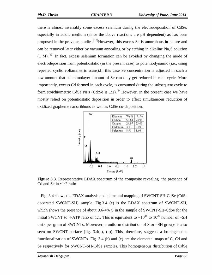
Ph.D. Thesis CHAPTER 3 University of Pune, June 2014
Joyashish Debgupta Page 66
there is almost invariably some excess selenium during the electrodeposition of CdSe,
especially in acidic medium (since the above reactions are pH dependent) as has been
proposed in the previous studies.[13]However, this excess Se is amorphous in nature and
can be removed later either by vacuum annealing or by etching in alkaline Na2S solution
(1 M).[13] In fact, excess selenium formation can be avoided by changing the mode of
electrodeposition from potentiostatic (in the present case) to potentiodynamic (i.e., using
repeated cyclic voltammetric scans).In this case Se concentration is adjusted in such a
low amount that submonolayer amount of Se can only get reduced in each cycle. More
importantly, excess Cd formed in each cycle, is consumed during the subsequent cycle to
form stoichiometric CdSe NPs (Cd:Se is 1:1).[14]However, in the present case we have
mostly relied on potentiostatic deposition in order to effect simultaneous reduction of
oxidized grapheme nanoribbons as well as CdSe co-deposition.
Figure 3.3. Representative EDAX spectrum of the composite revealing the presence of Cd and Se in ~1:2 ratio.
Fig. 3.4 shows the EDAX analysis and elemental mapping of SWCNT-SH-CdSe (CdSe
decorated SWCNT-SH) sample. Fig.3.4 (e) is the EDAX spectrum of SWCNT-SH,
which shows the presence of about 3.6-4% S in the sample of SWCNT-SH-CdSe for the
initial SWCNT to 4-ATP ratio of 1:1. This is equivalent to ~1018 to 1020 number of –SH
units per gram of SWCNTs. Moreover, a uniform distribution of S or –SH groups is also
seen on SWCNT surface (fig. 3.4(a), (b)). This, therefore, suggests a homogeneous
functionalization of SWCNTs. Fig. 3.4 (b) and (c) are the elemental maps of C, Cd and
Se respectively for SWCNT-SH-CdSe samples. This homogeneous distribution of CdSe

Ph.D. Thesis CHAPTER 3 University of Pune, June 2014
Joyashish Debgupta Page 67
perhaps indicates a successful ligand exchange and subsequent decoration of CdSe QDs
on SWCNT surface.
Figure 3.4. (a) SEM image and elemental mapping of (b) C (c) S and (d) Cd in SWCNT-SH-CdSe sample showing uniform distribution of the elements over SWCNT bundles, (e) EDAX spectrum of SWCNT-SH showing the percentage of the elements present.
3.4.3. TG analysis
In order to further confirm the chemical interaction between –PhSH group and SWCNT
surface, thermogravimetric experiments have been carried out. Accordingly, fig.3.5
shows the thermograms of pristine SWCNT (p-SWCNT) and SWCNT-SH (chemically
functionalized SWCNT) respectively. Interestingly, the decomposition profiles of p-
SWCNT and SWCNT-SH are different. For example, at 900°C, SWCNT-SH shows a
higher weight loss (~18%) than p-SWCNT (~10-12%) and thus provides conclusive
evidence for the presence of functional groups other than oxygen functionalities in
SWCNT-SH. This undoubtedly proves that chemical bonding occurs between 4-ATP and
RGO during diazotization. FTIR, EDAX and TGA analysis thus ostensibly confirms the
successful grafting of –SH group in SWCNT.

Ph.D. Thesis CHAPTER 3 University of Pune, June 2014
Joyashish Debgupta Page 68
Figure 3.5. A comparison of the decompositon profiles of p-SWCNT (black) and SWCNT-SH (red) in nitrogen atmosphere; lower retention in case of SWCNT-SH confirms the chemical bonding between –PhSH moiety and SWCNT surface. Thermogravimetric analysis has also been carried out in order to understand the
adsorption-desorption behaviour of CH3CN and CH2Cl2 on p-MWCNTs and oz-
MWCNTs respectively. Accordingly, fig.3.6 shows a comparison of thermograms of p-
MWCNTs and oz-MWCNTs in nitrogen atmosphere after soaking in acetonitrile and
dichloromethane respectively. Thermal profiles of p-MWCNT and oz-MWCNT (in N2 as
well as in air) have also been incorporated for comparison. Interestingly, the %weight of
both p- as well as oz-MWCNT is found to increase after soaking in the respective
solvents and the decrease in weight starts at much higher temperature as compared to that
of the reference samples. However, the nature of the plot and the amount of the %weight
loss are not the same for samples soaked in CH2Cl2 and CH3CN and the difference is
more significant for p- and oz-MWCNTs. This clearly indicates different types of
adsorption for the two liquids on CNTs and moreover the nature of adsorption seems to
change with the ozone treatment. One probable reason could be the chopping of CNTs
upon ozone treatment and thereby facilitating some liquids to get incorporated into the
capillary of CNTs (other than the grooves and interstices of ozone treated CNT bucky
paper) and those liquids may get desorbed at higher temperature or react with CNTs
resulting in the initial weight increment in TGA (for p-MWCNTs it is mostly the liquids
at the interstices of CNT bundles which might react with CNTs).

Ph.D. Thesis CHAPTER 3 University of Pune, June 2014
Joyashish Debgupta Page 69
Figure 3.6. Thermograms of (a) pristine MWCNTs and (b) ozonized MWCNTs after soaking and heating in dichloromethane and acetonitrile respectively; All measurements were performed in nitrogen atmosphere; TGA of p-MWCNT and oz-MWCNT in air are incorporated in the figure for comparison; Inset shows the enlarged view of the thermograms after soaking in acetonitrile and dichloromethane.
3.4.4. XPS analysis
In order to get better insight into the nature of interaction between acetonitrile and CNTs,
Figure 3.7. Core level N-1s spectrum showing the interaction of acetonitrile with CNT.

Ph.D. Thesis CHAPTER 3 University of Pune, June 2014
Joyashish Debgupta Page 70
XPS study can be very useful to understand the nature of intercations of various
molecules with CNT surface. Accordingly, fig.3.7 shows the N-1s core level spectrum
after acetonitrile adsorption on CNTs. The spectrum suggests that the amount of nitrogen
is extremely small especially when we consider the weak adsorption of acetonitrile
molecules during the experiment (leaving behind non-interacted acetonitrile). Hence, the
XP spectrum of N-1s apparently appears so noisy. However, deconvolution gives two
peaks at 398.1 eV and 400.0 eV respectively. The nitrogen of CH3CN has a binding
energy of 399.4 eV.[15] The first peak (398.1 eV) may be assigned to the N-atom of some
loosely-adsorbed acetonitrile while the second peak at higher binding energy indicates
electron donation from N-atom of CH3CN molecule to the CNT whereby the N-atom
becomes electron deficient and hence there is an upshift of N-binding energy. However,
it is difficult to conclude from these experiments whether acetonitrile interacts via π- π
interaction or directly via the donation of unshared electron (or follows both the way).
This interaction also supports the slow change of contact angle for p-MWCNT when a
drop of acetonitrile is put on its surface. Dichloromethane, on the other hand, cannot
interact in such a way because, it neitherhas π- electron to interact nor unshared electrons
to donate to CNT. Further, it is less polar in nature so that it is incapable of inducing
charge transfer to or from the CNTs. Thus dichloromethane gets very weakly adsorbed on
CNT surface to cause physical dampening of the phonon modes of CNTs which is
supported by the minor upshift (4 cm-1) of D and G bands upon wetting. In sharp contrast,
for oz-MWCNT, such an explanation no longer holds good, partly because of the opening
of the tips of CNTs after ozonolysis and partly because of the fact that π-electron cloud
on CNT gets reduced upon ozonolysis due to the formation of more sp3 carbon atoms on
its surface at the cost of sp2 carbon atoms. The open tips allow easy percolation of the
liquids inside the channels and therefore results in observed wetting dynamics.
3.4.5. Cyclic voltammetry (CV) Experiments
3.4.5.1. CV before and after unzipping of SWCNTs CV is extremely useful in understanding the unzipping process of SWCNT under
controlled potential conditions. Accordingly, fig. 3.8 shows the cyclic voltammograms of
SWCNTs (coated on a 2 mm Pt-disk electrode) before and after applying constant anodic
bias (0.8 V vs MMS) for 10 h in 0.5 M H2SO4. The peaks A1/C1 is attributed to quinone-
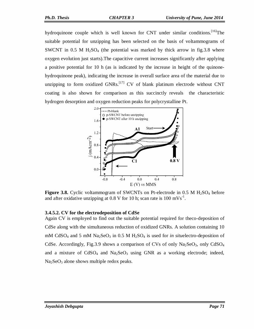
Ph.D. Thesis CHAPTER 3 University of Pune, June 2014
Joyashish Debgupta Page 71
hydroquinone couple which is well known for CNT under similar conditions.[16]The
suitable potential for unzipping has been selected on the basis of voltammograms of
SWCNT in 0.5 M H2SO4 (the potential was marked by thick arrow in fig.3.8 where
oxygen evolution just starts).The capacitive current increases significantly after applying
a positive potential for 10 h (as is indicated by the increase in height of the quinone-
hydroquinone peak), indicating the increase in overall surface area of the material due to
unzipping to form oxidized GNRs.[17] CV of blank platinum electrode without CNT
coating is also shown for comparison as this succinctly reveals the characteristic
hydrogen desorption and oxygen reduction peaks for polycrystalline Pt.
Figure 3.8. Cyclic voltammogram of SWCNTs on Pt-electrode in 0.5 M H2SO4 before and after oxidative unzipping at 0.8 V for 10 h; scan rate is 100 mVs-1.
3.4.5.2. CV for the electrodeposition of CdSe Again CV is employed to find out the suitable potential required for theco-deposition of
CdSe along with the simultaneous reduction of oxidized GNRs. A solution containing 10
mM CdSO4 and 5 mM Na2SeO3 in 0.5 M H2SO4 is used for in situelectro-deposition of
CdSe. Accordingly, Fig.3.9 shows a comparison of CVs of only Na2SeO3, only CdSO4
and a mixture of CdSO4 and Na2SeO3 using GNR as a working electrode; indeed,
Na2SeO3 alone shows multiple redox peaks.
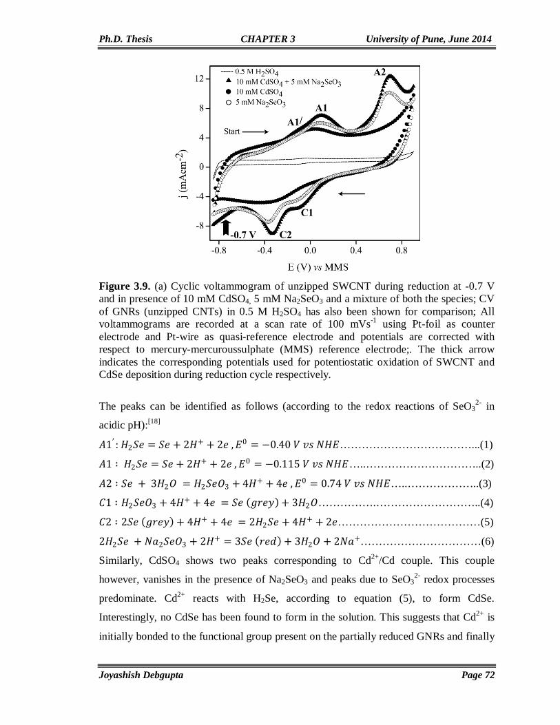
Ph.D. Thesis CHAPTER 3 University of Pune, June 2014
Joyashish Debgupta Page 72
Figure 3.9. (a) Cyclic voltammogram of unzipped SWCNT during reduction at -0.7 V and in presence of 10 mM CdSO4, 5 mM Na2SeO3 and a mixture of both the species; CV of GNRs (unzipped CNTs) in 0.5 M H2SO4 has also been shown for comparison; All voltammograms are recorded at a scan rate of 100 mVs-1 using Pt-foil as counter electrode and Pt-wire as quasi-reference electrode and potentials are corrected with respect to mercury-mercuroussulphate (MMS) reference electrode;. The thick arrow indicates the corresponding potentials used for potentiostatic oxidation of SWCNT and CdSe deposition during reduction cycle respectively.
The peaks can be identified as follows (according to the redox reactions of SeO32- in
acidic pH):[18]
𝐴𝐴1′ : 𝐻𝐻2𝑆𝑆𝑆𝑆 = 𝑆𝑆𝑆𝑆 + 2𝐻𝐻+ + 2𝑆𝑆 ,𝐸𝐸0 = −0.40 𝑉𝑉 𝑣𝑣𝑣𝑣 𝑁𝑁𝐻𝐻𝐸𝐸………………………………...(1)
𝐴𝐴1 ∶ 𝐻𝐻2𝑆𝑆𝑆𝑆 = 𝑆𝑆𝑆𝑆 + 2𝐻𝐻+ + 2𝑆𝑆 ,𝐸𝐸0 = −0.115 𝑉𝑉 𝑣𝑣𝑣𝑣 𝑁𝑁𝐻𝐻𝐸𝐸…..…………………………..(2)
𝐴𝐴2 ∶ 𝑆𝑆𝑆𝑆 + 3𝐻𝐻2𝑂𝑂 = 𝐻𝐻2𝑆𝑆𝑆𝑆𝑂𝑂3 + 4𝐻𝐻+ + 4𝑆𝑆 ,𝐸𝐸0 = 0.74 𝑉𝑉 𝑣𝑣𝑣𝑣 𝑁𝑁𝐻𝐻𝐸𝐸…..………………..(3)
𝐶𝐶1 ∶ 𝐻𝐻2𝑆𝑆𝑆𝑆𝑂𝑂3 + 4𝐻𝐻+ + 4𝑆𝑆 = 𝑆𝑆𝑆𝑆 (𝑔𝑔𝑔𝑔𝑆𝑆𝑔𝑔) + 3𝐻𝐻2𝑂𝑂…………….………………………..(4)
𝐶𝐶2 ∶ 2𝑆𝑆𝑆𝑆 (𝑔𝑔𝑔𝑔𝑆𝑆𝑔𝑔) + 4𝐻𝐻+ + 4𝑆𝑆 = 2𝐻𝐻2𝑆𝑆𝑆𝑆 + 4𝐻𝐻+ + 2𝑆𝑆…………………………………(5)
2𝐻𝐻2𝑆𝑆𝑆𝑆 + 𝑁𝑁𝑁𝑁2𝑆𝑆𝑆𝑆𝑂𝑂3 + 2𝐻𝐻+ = 3𝑆𝑆𝑆𝑆 (𝑔𝑔𝑆𝑆𝑟𝑟) + 3𝐻𝐻2𝑂𝑂 + 2𝑁𝑁𝑁𝑁+……………………………(6)
Similarly, CdSO4 shows two peaks corresponding to Cd2+/Cd couple. This couple
however, vanishes in the presence of Na2SeO3 and peaks due to SeO32- redox processes
predominate. Cd2+ reacts with H2Se, according to equation (5), to form CdSe.
Interestingly, no CdSe has been found to form in the solution. This suggests that Cd2+ is
initially bonded to the functional group present on the partially reduced GNRs and finally

Ph.D. Thesis CHAPTER 3 University of Pune, June 2014
Joyashish Debgupta Page 73
to form CdSe nanoparticles (QDs) on GNRs. However, reaction (6) often competes and
results in slight excess Se deposition on so formed CdSe QDs. This agrees with EDAX
and Raman observation of the hybrids. Reactions of SeO32- are highly pH sensitive as can
be seen from equation (1) to (6). But, since unzipping has been done in 0.5 M H2SO4, no
other pH has been tested for CdSe deposition. Temperature has been kept constant at 303
K. From the CV analysis it is clear that the SeO32- reduction is complete after -0.4 V (vs
MMS) and that the oxidized GNRs are completely reduced at a constant potential of -0.7
V (vs MMS). Hence, at -0.7 V simultaneous reduction of oxidized GNRs and formation
of CdSe is expected to occur.
3.4.6. Chronoamperometry
In order to determine the suitable potential for reduction and also to investigate the
mechanism of deposition, chronoamperometry has been performed for 100 s at two
different potentials (-0.33 V and -0.77 V vs MMS respectively), which are more negative
than the open circuit potential (OCP) of the system (-0.21 V vs MMS). Accordingly,
fig.3.10(a) shows the amperogram for the deposition. Both the plots show an initial sharp
decrease (within ~2 s) in current density perhaps due to double layer charging and also
due to parasitic (local) currents (not shown in the plot). The current transient then steadily
increases to show a shoulder (or hump) followed by a minor decrease to a certain value,
eventually reaching a plateau. The Peak maximum, however, increases and becomes
more pronounced as the deposition potential becomes more negative (-0.33 V to -0.7 V)
as has been predicted by classical nucleation theory.[19]Since the reduction of oxidized
SWCNT is carried out at -0.7 V, electrodeposition has also been carried out subsequently
at -0.7 V. In order to unravel the nucleation process, the current-time transient obtained at
-0.7 V, has been subdivided into 3 zones (fig. 3.10(a)) - I, II and III. Linearity of current
density vst-1/2 (fig.3.10(b)) for zone-I (i.e, before peak maximum) is indicative of
instantaneous 3D nuclei formation with hemispherical growth. There are two models
available to describe nucleation - instantaneous and progressive.[19-20]A plot of two
dimensionless numbers namely (i/im)2 and t/tm give information about either of the above
mechanisms.
( 𝑖𝑖𝑖𝑖𝑚𝑚
)2 = 1.9542𝑡𝑡𝑡𝑡𝑚𝑚
1 − exp[−1.2564 𝑡𝑡𝑡𝑡𝑚𝑚]2 ……………………………………………….(7)
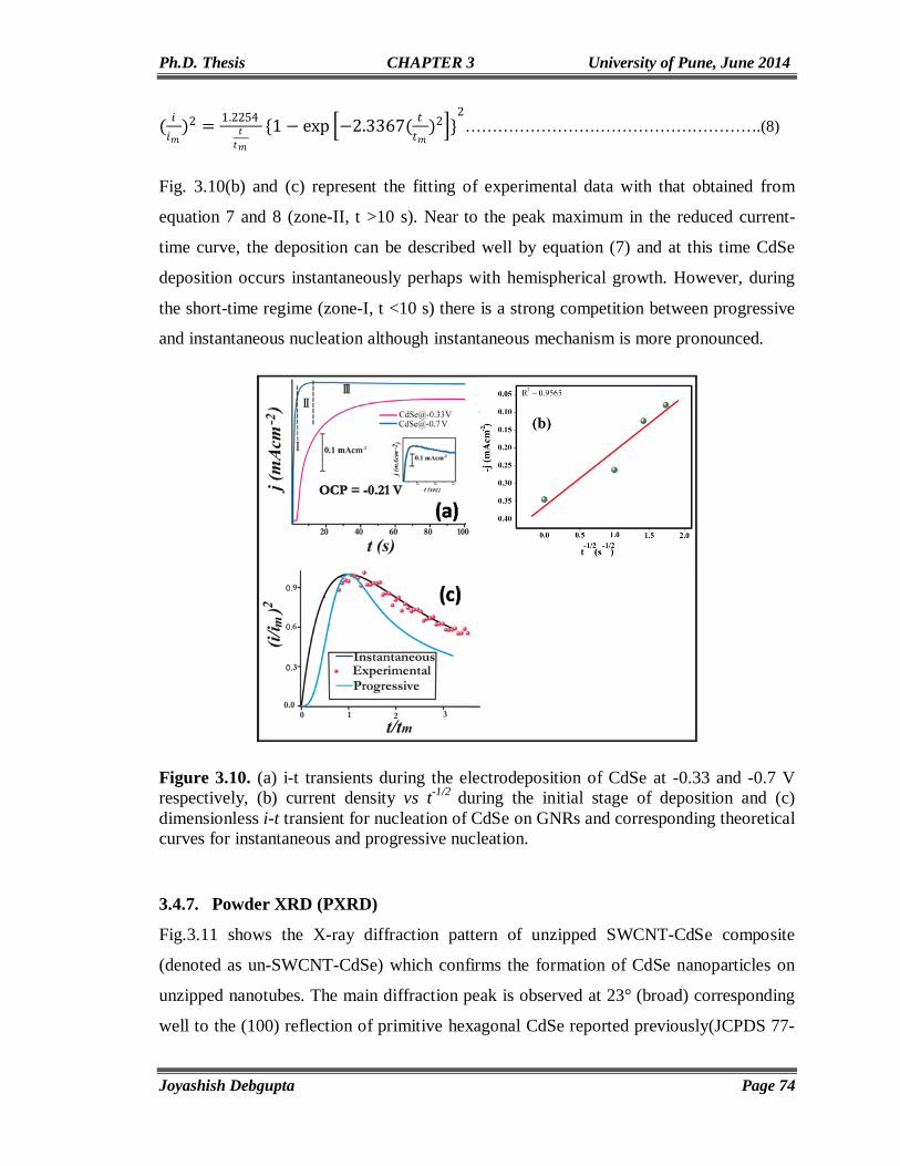
Ph.D. Thesis CHAPTER 3 University of Pune, June 2014
Joyashish Debgupta Page 74
( 𝑖𝑖𝑖𝑖𝑚𝑚
)2 = 1.2254𝑡𝑡𝑡𝑡𝑚𝑚
1 − exp −2.3367( 𝑡𝑡𝑡𝑡𝑚𝑚
)22……………………………………………….(8)
Fig. 3.10(b) and (c) represent the fitting of experimental data with that obtained from
equation 7 and 8 (zone-II, t >10 s). Near to the peak maximum in the reduced current-
time curve, the deposition can be described well by equation (7) and at this time CdSe
deposition occurs instantaneously perhaps with hemispherical growth. However, during
the short-time regime (zone-I, t <10 s) there is a strong competition between progressive
and instantaneous nucleation although instantaneous mechanism is more pronounced.
Figure 3.10. (a) i-t transients during the electrodeposition of CdSe at -0.33 and -0.7 V respectively, (b) current density vs t-1/2 during the initial stage of deposition and (c) dimensionless i-t transient for nucleation of CdSe on GNRs and corresponding theoretical curves for instantaneous and progressive nucleation.
3.4.7. Powder XRD (PXRD)
Fig.3.11 shows the X-ray diffraction pattern of unzipped SWCNT-CdSe composite
(denoted as un-SWCNT-CdSe) which confirms the formation of CdSe nanoparticles on
unzipped nanotubes. The main diffraction peak is observed at 23° (broad) corresponding
well to the (100) reflection of primitive hexagonal CdSe reported previously(JCPDS 77-

Ph.D. Thesis CHAPTER 3 University of Pune, June 2014
Joyashish Debgupta Page 75
0046).[21] Other broad peaks (at 36.5°, 42.8°, 49.4° and 56.3°) also match very well with
the same crystal structure of CdSe. The (002) peak of SWCNT/graphitic structure is
overlapped with the (100) peak of CdSe and hence is not clearly visible. In fact, the
appearance of so many peaks proves the polycrystalline nature of CdSe particles and the
broadening of the XRD peaks reveals that the particles are in the nanometer range.
Figure 3.11. Powder X-ray diffractograms of the CdSe-unzipped SWCNT composite prepared in situ. Diffraction peaks of un-SWCNT-CdSe match with the primitive hexagonal phase of CdSe and thus confirms the formation of CdSe.
3.4.8. Contact angle measurement
A detailed contact angle study has been carried out in order to understand the surface
properties of CNTs, i.e., surface energy changes due to adsorption, which is very useful
in designing new functionalization strategy as well as processability. Acetonitrile
(CH3CN) and dichloromethane (CH2Cl2) have been chosen as model molecules for the
study as these two molecules differ in physical (viz. dipole moment, surface tension,
viscosity etc.), molecular and electronic properties. More significantly, these results can
be used to compare with that of the CdSe QDs-CNT interactions, because QD is also
thought of as a giant artificial atom (it shows atom like properties). Accordingly, wetting
behavior of acetonitrile and dichloromethane on MWCNT surfaces has been depicted in
fig.3.12 along with that of water for comparison. Surface roughness is a critical

Ph.D. Thesis CHAPTER 3 University of Pune, June 2014
Joyashish Debgupta Page 76
contributing factor in explaining the results of these experiments. Hence, macroscopic
surface roughness has been tried to keep at its minimum by pressing each CNT paper
(bucky paper) sample between two glass-plates in an identical fashion although it is
difficult to control the microscopic roughness all the time. Fig.3.12 shows that water does
not wet the surface of both pristine as well as ozonized MWCNT and the contact angle
values are invariant with time, although oz-MWCNT shows super-hydrophobicity with
contact angles ~158°-160°unlike 112°-114° for p-MWCNTs. This super-hydrophobicity
has been attributed in part to the more compact nature of the oz-CNT paper with very
small pore sizes and also due to the generation of hydrophobic ester groups which repel
the water and causes it to bounce back from the oz-CNT surface.[22] High surface tension
of water (72 mNm-1 at 20°C) is another factor for this contact angle variation. Water is a
highly polar liquid (µ = 6.2 Debye) and exists as a network of water molecules through
H-bonding and not as discrete water molecules. Naturally, it has a very low value of
dispersive component and that is why it cannot penetrate through the inter-tubular gaps of
CNT bundles (both p-and oz-MWCNT) resulting in non-wetting situation. The ester
group derived from the ozonolysis further restricts the penetration of water molecules and
causes super-hydrophobicity.
Figure 3.12. Wetting behavior of water (H2O), acetonitrile (CH3CN) and dichloromethane (CH2Cl2) on p-MWCNT () as well as oz-MWCNT ()(Y-axis error

Ph.D. Thesis CHAPTER 3 University of Pune, June 2014
Joyashish Debgupta Page 77
bar = ± 2°).
Acetonitrile (CH3CN), on the other hand, completely wets the CNT surfaces. However,
the wetting process shows interesting dynamics on p-and oz-MWCNT surfaces. As
fig.3.12 suggests, acetonitrile shows a time dependent wetting pattern on p-MWCNT
surface. More specifically, there is a gradual decrease in contact angle of acetonitrile
from an initial value of ca.25.8°±2°over a period of ~50 sec in case of pristine-MWCNT
(p-CNT) until it reaches 0°(Complete wetting). But contact angle of acetonitrile abruptly
decreases from an initial value of 38.9°± 2° to 0° almost immediately (< 1 sec from the
moment of droplet dispense of the drop) on oz-MWCNT (instantaneous wetting). Parallel
but distinctly different behavior is observed also in case of wetting by dichloromethane
(CH2Cl2), although the dynamics is pretty fast (< 400 ms) for both p-CNT and oz-CNT
unlike the case for acetonitrile. Instantaneous contact angles in these cases are 13.4°
±2°and 21.8°±2°for p-CNT and oz-CNT respectively. Surface tension of acetonitrile
(19.10 mNm-1 at 20°C) is less than that of dichloromethane (26.50 mNm-1 at 20°C). This
means that acetonitrile should spread more rapidly than dichloromethane on CNT
surface, i.e., lower contact angle than dichloromethane according to Young’s equation.,
𝑐𝑐𝑐𝑐𝑣𝑣𝜃𝜃𝑐𝑐 = 𝛾𝛾𝑆𝑆𝑉𝑉 −𝛾𝛾𝐿𝐿𝑆𝑆𝛾𝛾𝑉𝑉𝐿𝐿
…….(9)
Where, γSV, γLS and γLV are the solid-vapor, liquid-solid and liquid-vapor surface tensions
respectively and θe is the apparent contact angle (experimental contact angle). Hence, the
different wetting behavior cannot be explained solely by taking into account the surface
tension and capillary effect. In practice, the solid-liquid interfacial energy (γLS) is
governed by many forces like van der Waals, hydrogen-bonding and dipolar, and a
resultant of all these competing interactions determines the spreading of a liquid over a
surface. Actually, the interactions of the liquids with the CNTs seem to be responsible for
those interesting wetting dynamics in case of dichloromethane and acetonitrile (though it
is difficult to draw a molecular level picture by observing macroscopic property like
apparent contact angle, a probable interpretation can be obtained by combining with other
experimental data like spectroscopic evidence and so on). Dichloromethane is a relatively
lesspolar liquid with a very low dipole moment of 1.60 D as compared to that of 3.92 D

Ph.D. Thesis CHAPTER 3 University of Pune, June 2014
Joyashish Debgupta Page 78
in case of acetonitrile. Theoretical calculations suggest the dispersive components of 17.0
and 15.3 and a polar component of 7.3 and 18.0 for dichloromethane and acetonitrile
respectively. This means dispersive forces are more pronounced in dichloromethane. On
the other hand, dipole-dipole interactions prevail in acetonitrile, as is revealed from X-ray
diffraction and that results in a zigzag chain of acetonitrile molecules by an antiparallel
dipole-dipole interaction.[23] This situation is, thus similar, although little different, to the
long network of water molecules. Due to this more dispersive nature than acetonitrile,
dichloromethane exists as discrete molecules which are much smaller in size than the
dimension of the inter-tubular gaps and, therefore, can penetrate more easily into the
inter-tubular gaps of the CNT papers and thereby results in instantaneous wetting both in
case of p-CNT as well as oz-CNT unlike the situation for acetonitrile. Now, the change of
the mode of wetting on two surfaces (p-CNT and oz-CNT) can be rationalized in terms of
the opening of the tips of CNTs caused by the oxidation during ozonolysis in case of oz-
CNT. Liquids can easily penetrate into the channels of oz-CNTs through the open tips
and that probably is observed as instantaneous wetting. Somewhat higher momentary
contact angle in case of oz-CNTs than p-CNTs can be understood by the momentary
hindrance or hydrophobic interaction of the liquids (-CH3 in case of CH3CN and -CH2 for
CH2Cl2) with the dangling –COOCH3 groups which causes superhydrophobicity in case
of water droplet.[22] The value of contact angle (instantaneous contact angle) is more for
acetonitrile than for dichloromethane because –CH3 group is less polarizable and hence
more hydrophobic than –CH2 group. This may also be due to the more compact
interconnected nature of the bucky paper obtained after ozonolysis of MWCNT. The
wetting behaviors have been summarized in table 3.1, which shows comparative values
of contact angles for water, CH3CN, CH2Cl2 (both initial and final) and thus reflects the
different types of interactions.
Table 3.1. Variation in contact angle of water, acetonitrile and dichloromethane on Pristine and ozonized MWCNTs; surface tension values of all the solvents have been given for comparison. Before measurements, all samples are compacted under identical conditions to get smooth surface so as to minimize errors due to surface roughness.

Ph.D. Thesis CHAPTER 3 University of Pune, June 2014
Joyashish Debgupta Page 79
Sample Liquid Surface Tension (γ) mNm-1 at 20°C
Initial value of contact angle (°)
Final value of contact angle (°)
Time of measurement (s)
Time for complete spreading (s)
Pristine CNT
Water 72 114 114 90 Does not spread
Acetonitrile 19.10 25.8 0 90 50
Dichloromethane 26.50 13.4 0 90 0.28
Ozonized CNT
Water 72 158-160 158-160 90 Does not spread
Acetonitrile 19.10 38.9 0 90 Instantaneous
Dichloromethane 26.50 21.8 0 90 0.17
3.4.9. Micro Raman
Raman scattering is used extensively to probe the interaction of CH3CN and CH2Cl2 with
CNT as well as to characterize SWCNT-SH-CdSe and GNR-CdSe hybrids. Accordingly,
fig.3.13(A) shows a comparison of the Micro Raman spectra of p-CNT and oz-CNT
samples. However, after the ozone treatment, G-band intensity drops down significantly
ensuring the breaking of graphitic structure during ozonolysis. As a result, ID to IG ratio
increases from 0.61 to 0.76 on ozonolysis indicating more defect formation (more sp3
than sp2 carbons as compared to that on p-MWCNT) on the side-walls of MWCNTs and
thereby causes changes in its electronic structure. In comparison fig.3.13(B) represents
the micro Raman spectra of p-MWCNT and oz-MWCNT after wetting experiment by
acetonitrile and dichloromethane. Raman spectra show a D and G band shift of ~13 cm-1
and 4 cm-1 on wetting by acetonitrile and dichloromethane respectively in case of p-
CNTs. Interestingly, there is no such shift in case of oz-CNTs. Moreover, acetonitrile

Ph.D. Thesis CHAPTER 3 University of Pune, June 2014
Joyashish Debgupta Page 80
causes upshift while dichloromethane causes downshift of the corresponding bands of p-
CNTs. Indeed, D (defective) and G (graphitic) are two tangential modes of phonon
vibrations in CNTs and these two modes are characteristics of sp3 and sp2 type of C-C
bonding respectively. A shift in the positions of these bands thus, really indicates
vibrational energy transfer between CNTs and the liquid molecules.
Figure 3.13. (a) Superimposed Micro Raman Spectra of pristine (p-MWCNT) and ozonized (oz-MWCNT) carbon nanotubes showing the rupture of the C=C backbone during ozonolysis to form –COOCH3 groups; (b) and (c) Micro Raman spectra during the wetting experiments by acetonitrile and dichloromethane respectively; Acetonitrile on (I)

Ph.D. Thesis CHAPTER 3 University of Pune, June 2014
Joyashish Debgupta Page 81
p-CNT (III) oz-CNT and dichloromethane on (II) p-CNT and (IV) oz-CNT measured using 632.8 nm LASER.
Many types of experimental evidences suggest a shift in Raman band positions of
CNTs on charge transfer to or from the CNTs (as a result of doping).[24] In case of p-type
doping, electrons are taken away from the CNT and thereby causing an upshift of the
band while, similar n-type doping pushes charges on CNT causing a concomitant
downshift in both D and G band. However, CNTs are a huge reservoir of mobile π-
electrons and acetonitrile (CH3CN) having –C≡N π bond can interact with th is π-cloud
through π- π interaction. The non-bonded electrons on N-atom can also be donated to the
CNT and this causes n-type doping of CNTs and that is manifested in the form of red-
shift in D and G frequencies from their original position in CNT on wetting by
acetonitrile. This is confirmed from the value of the shift (13 cm-1 = 2 meV) which is
equivalent to the interaction energy for the weakly adsorbing acetonitrile molecules. It
has been shown that binding energies for benzonitrile molecule to SWCNT and graphene
surface vary from 10meV to 60meV depending upon the orientation of the benzonitrile
molecule with respect to the SWCNT or grapheme surface (i.e., π-π or π-C≡N
interaction).[25] Acetonitrile (CH3CN) having no benzene ring for strong π-π interaction
like benzonitrile (PhCN), can only interact via -C≡N π-bond or nitrogen lone pair andthat
explains the less binding energy for CH3CN unlike benzonitrile. It, thus appears that
acetonitrile molecules form a thin film on CNT after spreading and transfer vibrational
energy electronically to the CNTs is likely affecting a change in vibrational frequency of
the CNTs. Dichloromethane (CH2Cl2) molecule, however, does not have any charge
transfer component to interact like CH3CN and vibrational bands (Raman bands),
therefore, are not affected significantly. Interestingly, there is no change in position either
of D or G band of oz-MWCNT on wetting by both of the liquids (Fig.3.13(B)). This is
somewhat contradictory to what reported by Nelson et al.20 where molecules inside the
CNTs are more efficient in transferring vibrational energy with the CNT than the
molecules around it, because afterozonolysis the shorter and open-ended CNTs can allow
the solvent molecules (CH3CN and CH2Cl2) to go in. Moreover, covalent
functionalization disrupts the π-clouds and the possibility of π-π interaction reduces and
so there is little or almost no change in the D or G band positions in case of oz-MWCNT
Ph.D. Thesis CHAPTER 3 University of Pune, June 2014
Joyashish Debgupta Page 82
even with CH3CN.
In order to confirm the unzipping of SWCNT and subsequent deposition of CdSe on
them under electrochemical conditions, we have carried out micro Raman study at
various stages of the unzipping process concomitant to the CdSe anchoring. Accordingly,
fig.3.14 describes the micro Raman spectra for (i) pristine SWCNT before unzipping, (ii)
SWCNT on subjecting to 0.8 V, (iii) GNRs after CdSe decoration at -0.7 V. The intensity
ratio of the two phonon modes, namely D-band and G-band, is found to increase from
0.08 to 0.86 after the SWCNTs are subjected to 0.8 V for 10 h. This indicates the increase
of defects after electrochemical oxidation. More striking feature of the Raman spectra is
the disappearance of the so called RBM band of pristine SWCNT (258.1 cm-1
corresponding to metallic nanotubes) on 6 h oxidation. This is in agreement with the
observed report that metallic CNTs are more susceptible towards electronic attack than
their semiconductor analogues.[26] Other two RBM phonon modes (due to
semiconducting nanotubes) also decrease in intensity–strongly suggesting the opening of
CNTs (unzipping) with the concomitant formation of graphene nanoribbons. The
application of external anodic potential modulates the Fermi level of CNTs and allows
oxidative unzipping. In fact, anodic bias gives rise to defect sites which thereby disrupts
the symmetry of electron distribution on CNTs rendering the surrounding carbon atoms
more reactive. This activation helps to propagate the defects along the tubular axis of
CNT and eventually opens up the nanotubes to form graphene. However, the Raman
spectrum is different after in situ CdSe decoration, specially in the low frequency region
(Fig.3.14(iii)). The spectrum clearly shows the presence of CdSe NPs. On the low
frequency region (210-300 cm-1 inset of fig.3.14(ii)), peak corresponding to LO phonon
of CdSe NPs (205 cm-1) has been observed. Appearance of LO phonon at 205 cm-1 as
compared to that in case of bulk CdSe (210 cm-1) suggests the formation of nanosized
clusters of CdSe on GNRs.[27] Moreover, a broad two photon 2LO band for CdSe NPs is
also observed at 408 cm-1. The peak at 238 cm-1 can be assigned to ν10 (ε3) mode of
phonon vibration of amorphous selenium conforming the presence of excess selenium
during electrodeposition.[28]

Ph.D. Thesis CHAPTER 3 University of Pune, June 2014
Joyashish Debgupta Page 83
Figure 3.14. Superimposed Micro Raman spectra of (i) pristine SWCNT (before unzipping), (ii) SWCNT after unzipping at 0.8 V for 10 h and (iii) unzipped SWCNT after CdSe decoration at -0.7 V; All the spectra are recorded with 632.8 nm laser with 20 mW power.
On the other hand, Raman spectra of SWCNT-SH and SWCNT-SH-CdSe show (fig.
3.15) characteristic radial breathing modes of vibrations (RBM bands) in the region 100-
300 cm-1for the presence of SWCNTs other than the normal D and G bands. The RBM
bands remain intact even upon functionalization and CdSe QD attachment suggesting its
stability as even partial unzipping can alter this.[26] This proves that the electronic
structure and morphology of SWCNTs is not affected by the functionalization or CdSe
decoration. The 2D band which is the overtone of D-band (~at 2600 cm-1) is also
unaffected by functionalization. It also indirectly suggests that SWCNTs undergo
longitudinal unzipping upon applying electrochemical potential for 10 h.
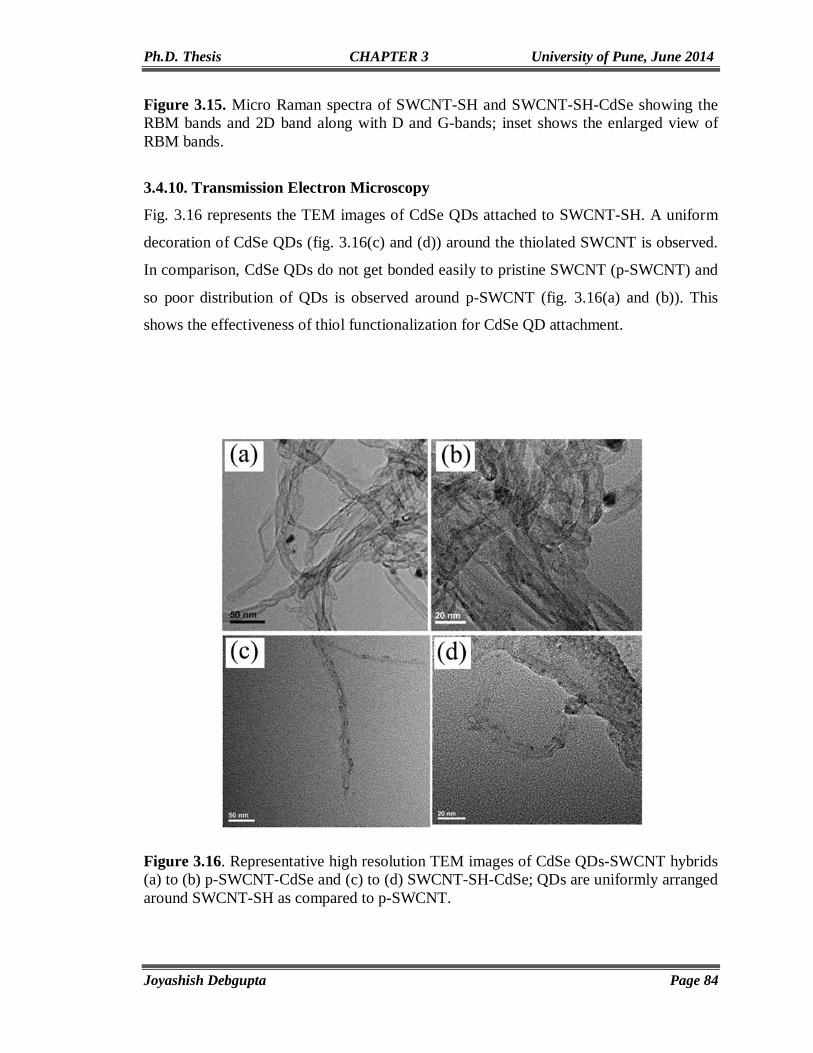
Ph.D. Thesis CHAPTER 3 University of Pune, June 2014
Joyashish Debgupta Page 84
Figure 3.15. Micro Raman spectra of SWCNT-SH and SWCNT-SH-CdSe showing the RBM bands and 2D band along with D and G-bands; inset shows the enlarged view of RBM bands.
3.4.10. Transmission Electron Microscopy
Fig. 3.16 represents the TEM images of CdSe QDs attached to SWCNT-SH. A uniform
decoration of CdSe QDs (fig. 3.16(c) and (d)) around the thiolated SWCNT is observed.
In comparison, CdSe QDs do not get bonded easily to pristine SWCNT (p-SWCNT) and
so poor distribution of QDs is observed around p-SWCNT (fig. 3.16(a) and (b)). This
shows the effectiveness of thiol functionalization for CdSe QD attachment.
Figure 3.16. Representative high resolution TEM images of CdSe QDs-SWCNT hybrids (a) to (b) p-SWCNT-CdSe and (c) to (d) SWCNT-SH-CdSe; QDs are uniformly arranged around SWCNT-SH as compared to p-SWCNT.
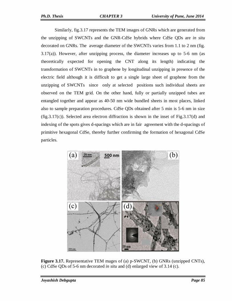
Ph.D. Thesis CHAPTER 3 University of Pune, June 2014
Joyashish Debgupta Page 85
Similarly, fig.3.17 represents the TEM images of GNRs which are generated from
the unzipping of SWCNTs and the GNR-CdSe hybrids where CdSe QDs are in situ
decorated on GNRs. The average diameter of the SWCNTs varies from 1.1 to 2 nm (fig.
3.17(a)). However, after unzipping process, the diameter increases up to 5-6 nm (as
theoretically expected for opening the CNT along its length) indicating the
transformation of SWCNTs in to graphene by longitudinal unzipping in presence of the
electric field although it is difficult to get a single large sheet of graphene from the
unzipping of SWCNTs since only at selected positions such individual sheets are
observed on the TEM grid. On the other hand, fully or partially unzipped tubes are
entangled together and appear as 40-50 nm wide bundled sheets in most places, linked
also to sample preparation procedures. CdSe QDs obtained after 5 min is 5-6 nm in size
(fig.3.17(c)). Selected area electron diffraction is shown in the inset of Fig.3.17(d) and
indexing of the spots gives d-spacings which are in fair agreement with the d-spacings of
primitive hexagonal CdSe, thereby further confirming the formation of hexagonal CdSe
particles.
Figure 3.17. Representative TEM mages of (a) p-SWCNT, (b) GNRs (unzipped CNTs), (c) CdSe QDs of 5-6 nm decorated in situ and (d) enlarged view of 3.14 (c).

Ph.D. Thesis CHAPTER 3 University of Pune, June 2014
Joyashish Debgupta Page 86
However, small particles further grow, in presence of excess precursor, with the
time of deposition and eventually form large clusters, typically after 1 h. These particles
are 15-20 nm after 15 min and become 40-50 nm clusters after 1 h to eventually cover
the GNRs (Fig. 3.18 (a) and (b)).
Figure 3.18. Representative TEM mages of GNRs during CdSe deposition, (a) deposition time 15 min (b) deposition time 1 h; CdSe particle size increases with time.
Thus TEM analysis suggests that CdSe QDs can be organized on GNR without
any bifunctional linker molecule. The residual functionality in GNR most probably helps
to bind the CdSe formed during electrodeposition.
3.4.11. UV-Vis Absorption and Photoluminescence (PL)
UV-Vis absorption and photoluminescence studies have been carried out to explore the
properties of the hybrids made up of CdSe and carbon nanostructures, mainly SWCNT
and un-SWCNTs (GNRs) derived from SWCNT. CdSe QDs alone show a peak
corresponding to 1Sh-1Se transition as has been discussed in the preceding chapters. On
the other hand, SWCNT shows multiple small peaks (undulations) in the absorbance
spectrum. These undulations are called Van Hove’s singularities which originate due to
transitions within the discrete molecular type states in the band structure of SWCNTs.
For example, fig. 3.19(a) shows the absorbance plots of p-SWCNTs and un-SWCNTs
(GNRs) after in situ CdSe decoration. p-SWCNT sample shows features of Van Hove’s
singularities which vanish after unzipping and a new peak emerges out at 576 nm which
is the characteristic peak for CdSe QDs having size of 4-5 nm. Disappearance of the
features of SWCNT suggests the change in electronic properties due to the application of
electrical potential (unzipping). On the other hand, PL emission spectrum of the hybrid of

Ph.D. Thesis CHAPTER 3 University of Pune, June 2014
Joyashish Debgupta Page 87
CdSe-GNR (fig. 3.19(b)) upon excitation with 480 nm wavelength does not give any
peak, whereas oleic acid capped CdSe QDs having 4-5 nm diameter, show a sharp PL
emission under similar conditions. In presence of GNR, therefore, quenching of CdSe PL
takes place and this is due to the proper band alignment between CdSe QDs and GNRs.
This clearly indicates that GNR acts as an electron acceptor in this case.
Figure 3.19. (a) Absorption and (b) Solid state Photoluminescence spectra of the CdSe QDs-GNR hybrids. Excitation wavelength is 480 nm for PL.
Similarly, when SWCNT-SH is gradually added to a solution of oleic acid capped
CdSe QDs (4 nm size), the PL emission intensity of the latter is gradually reduced to zero
(fig. 3.20(a)). This is because CdSe QDs get bonded to –SH group of SWCNT-SH via
ligand exchange and thus establishes a direct link between SWCNT and QDs levels. So,
charge transfer can easily occur from excited CdSe QD to SWCNT resulting in observed
PL quenching. On the other hand, p-SWCNT is not much effective in quenching the PL
of CdSe QD because of immiscibility of SWCNT suspension (poorly dispersed DMF
suspension) and toluene solution of CdSe QDs (fig. 3.20(b)). This is more because no
direct contact is possible in case of p-SWCNT-CdSe QDs unlike the SWCNT-SH case.
Insulating oleic acid is responsible for hindrance to this electron transfer.

Ph.D. Thesis CHAPTER 3 University of Pune, June 2014
Joyashish Debgupta Page 88
Figure 3.20. PL quenching experiment of CdSe QDs (4 nm) using (a) p-SWCNT and (b) SWCNT-SH; SWCNT-SH is found to be a better quencher because of the presence of –SH group which binds to CdSe QDs.
Thus it is clear from the combined results of a UV-Vis and PL study that free
CdSe QDs and those bound to some carbon nanostructures behave differently. Electronic
property of the QD remains unaffected as is evident from UV-Vis absorbance, but its
emission property is severely affected due to charge transfer. Moreover, bound CdSe
QDs are effective in transferring charge from excited QDs to the carbon nanostructures
rather than the free QDs in solution in contact with carbon nanostructures. In fact, similar
phenomenon has already been discussed in the preceding section (3.4.8) where only
acetonitrile has been found to be strongly adsorbed on CNT surface, due to its capability
of charge transfer to CNT, unlike that of dichloromethane because of its
weakadsorption on CNT. The only difference between the two is that CdSe QDs can
transfer charge to CNTs when activated by external photon (photo-induced charge
transfer); whereas acetonitrile can do the same without activation by light. The
combination of CdSe QDs and carbon nanostructure, therefore, can give rise to important
hybrids for the application of various optoelectronic devices.
3.4.12. Photoconductivity study
In order to prove the efficiency of the hybrid materials discussed above,
photoconductivity measurement has been performed. Accordingly, fig.3.21reveals the
representative I-V curve for CdSe-GNR hybrid in the presence and absence of light
(AM1.5 solar simulated light). The plot shows Ohmic behavior at very low voltage range
(±0.2 V), although subsequently this changes to Schottky type at voltages more than ±0.2
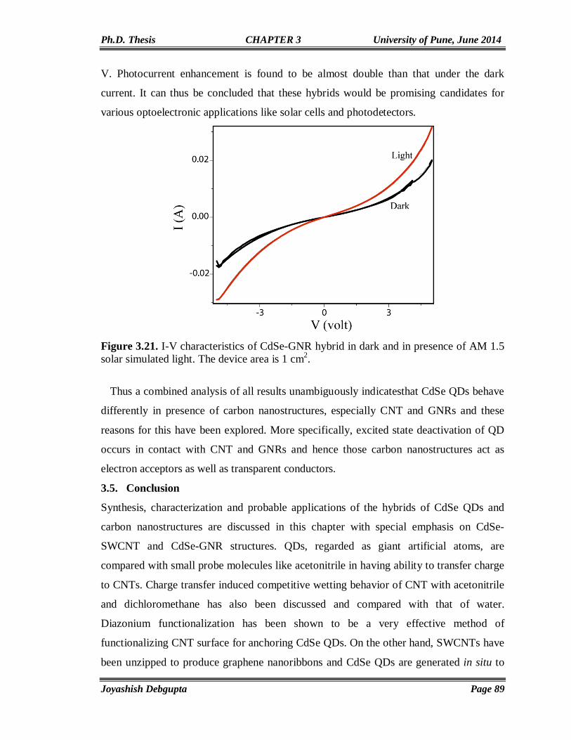
Ph.D. Thesis CHAPTER 3 University of Pune, June 2014
Joyashish Debgupta Page 89
V. Photocurrent enhancement is found to be almost double than that under the dark
current. It can thus be concluded that these hybrids would be promising candidates for
various optoelectronic applications like solar cells and photodetectors.
Figure 3.21. I-V characteristics of CdSe-GNR hybrid in dark and in presence of AM 1.5 solar simulated light. The device area is 1 cm2.
Thus a combined analysis of all results unambiguously indicatesthat CdSe QDs behave
differently in presence of carbon nanostructures, especially CNT and GNRs and these
reasons for this have been explored. More specifically, excited state deactivation of QD
occurs in contact with CNT and GNRs and hence those carbon nanostructures act as
electron acceptors as well as transparent conductors.
3.5. Conclusion
Synthesis, characterization and probable applications of the hybrids of CdSe QDs and
carbon nanostructures are discussed in this chapter with special emphasis on CdSe-
SWCNT and CdSe-GNR structures. QDs, regarded as giant artificial atoms, are
compared with small probe molecules like acetonitrile in having ability to transfer charge
to CNTs. Charge transfer induced competitive wetting behavior of CNT with acetonitrile
and dichloromethane has also been discussed and compared with that of water.
Diazonium functionalization has been shown to be a very effective method of
functionalizing CNT surface for anchoring CdSe QDs. On the other hand, SWCNTs have
been unzipped to produce graphene nanoribbons and CdSe QDs are generated in situ to

Ph.D. Thesis CHAPTER 3 University of Pune, June 2014
Joyashish Debgupta Page 90
make CdSe-GNR hybrids. All these hybrids show efficient PL quenching and perhaps a
good photoresponse indicating their ability to serve as next generation optoelectronic
materials.
3.6. References
1. (a) Reimann, S. M.; Manninen, M. Rev. mod. phys. 2002, 74, 1283. (b) Brus, L. J.
Phys. Chem. 1986, 90, 2555.
2. Nozik, A. J. Chem. Phys. Lett. 2008, 457(1), 3-11.
3. (a) Konstantatos, G.; Howard, I.; Fischer, A.; Hoogland, S.; Clifford, J.; Klem, E.;
Levina, L.; Sargent, E. H. Nature 2006 442(7099), 180. (b) Oertel, D. C.; Bawendi,
M. G.; Arango, A. C.; Bulović, V. Appl. Phys. Lett. 2005, 87(21), 213505. (c) Kim,
J. Y.; Voznyy, O.; Zhitomirsky, D.; Sargent, E. H. Adv. Mater. 2013, 25, 4986. (d)
Tang, A. W.; Teng, F.; Hou, Y. B.; Xiong, S.; Feng, B.; Qian, L.; Wang, Y. S. J.
Nanosci. Nanotechno. 2008, 8, 1330. (e) Zhao, L. J.; Hu, L. F. Pure Appl. Chem.
2012, 84, 2549.
4. (a) Lu, L. L.; Hou, W. J.; Sun, J.; Wang, J. J.; Qin, C. X.; Dai, L. X. J. Mat. Sci. 2014,
49, 3322. (b) Wei, H.; Li, Z. Q.; Xiong, D. B.; Tan, Z. Q.; Fan, G. L.; Qin, Z.; Zhang,
D. Scripta Mater.2014, 75, 30. (c) Lee, C.; Wei, X.; Kysar, J. W.; Hone, J. Science
2008, 321, 385. (d) Han, J.; Ryu, S.; Sohn, D.; Im, S. Carbon 2014, 68, 250. (e)
Shokrieh, M. M.; Esmkhani, M.; Vahedi, F.; Shahverdi, H. R. Ira. Pol. J. 2013, 22,
721. (f) Zhu, K. K.; Sun, J. M.; Zhang, H.; Liu, J.; Wang, Y. J. Nat. Gas Chem. 2012,
21, 215.
5. (a) Schlogl, R.: Carbon in Catalysis. In Advances in Catalysis, Vol 56; Gates, B. C.,
Jentoft, F. C., Eds.; Elsevier Academic Press Inc: San Diego, 2013; Vol. 56; pp 103.
(b) Choi, H. J.; Jung, S. M.; Seo, J. M.; Chang, D. W.; Dai, L. M.; Baek, J. B. Nano
Energy 2012, 1, 534. (c) Wan, X. J.; Huang, Y.; Chen, Y. S. Acc. Chem. Res. 2012,
45, 598. (d) Singh, V.; Joung, D.; Zhai, L.; Das, S.; Khondaker, S. I.; Seal, S. Prog.
Mater Sci. 2011, 56, 1178. (e) Falcao, E. H. L.; Wudl, F. J. Chem. Technol.
Biotechnol. 2007, 82, 524.
6. (a) Wang, Q. H.; Bellisario, D. O.; Drahushuk, L. W.; Jain, R. M.; Kruss, S.; Landry,
M. P.; Mahajan, S. G.; Shimizu, S. F. E.; Ulissi, Z. W.; Strano, M. S. Chem. Mater.

Ph.D. Thesis CHAPTER 3 University of Pune, June 2014
Joyashish Debgupta Page 91
2014, 26, 172. (b) Wang, Q.; Arash, B. Comput. Mat. Science 2014, 82, 350. (c)
Berman, D.; Erdemir, A.; Sumant, A. V. Mater. Today 2014, 17, 31. (d) Tovee, P. D.;
Pumarol, M. E.; Rosamond, M. C.; Jones, R.; Petty, M. C.; Zeze, D. A.; Kolosov, O.
V. Phys. Chem. Chem. Phys. 2014, 16, 1174. (e) Wang, F.; Zhao, J. B.; Gong, J. M.;
Wen, L. L.; Zhou, L.; Li, D. F. Chem. Eur. J. 2012, 18, 11804.
7. Kakade, B. A.; Pillai, V. K. Appl. Surf. Sci. 2008, 254, 4936.
8. (a) Shinde, D. B.; Debgupta, J.; Kushwaha, A.; Aslam, M.; Pillai, V. K.: J. Am. Chem.
Soc. 2011, 133, 4168. (b) Debgupta, J.; Shinde, D. B.; Pillai, V. K. Chem. Commun.
2012, 48, 3088.
9. Kakade, B. A; Allouche, H.; Mahima, S.; Sathe, B. R.; Pillai, V. K. Carbon 2008, 46,
567.
10. Sbai, K.; Rahmani, A.; Chadli, H.; Bantignies, J. L.; Hermet, P.; Sauvajol, J. L. J.
Phys. Chem. B, 2006, 110, 12388.
11. (a) Shirley, D. A. Phys. Rev. B 1972, 5, 4709 (b) Oberlin, A.; Endo M.; Koyama, T. J.
Crystal. Growth 1976, 32, 335.
12. (a) Mawhinney, D. B.; Naumenko, V.; Kuznetsova, A.; Yates Jr. J. T.; Liuand, J.;
Smalley, R. E. J. Am. Chem. Soc. 2000, 122, 2383. (b) Skakalova, S. V.; Kaiser, A.
B.; Weglikowska, D. U.; Hrncarikova, K.; Roth, S. J. Phys. Chem. B 2005, 109,
7174.
13. (a) Natarajan, C.; Sharon, M.; Levyclement, C.; Neumannspallart, M. Thin Solid
Films 1994, 237, 118. (b) Majidi, H.; Baxter, J. B. Electrochim. Acta 2011, 56, 2703.
14. Kressin, A. M.; Doan, V. V.; Klein, J. D.; Sailor, M. J. Chem. Mater. 1991, 3, 1015.
15. Schaff, Jason E.; Jeffrey T. Roberts. Surf. sci. 1999, 426.3, 384.
16. Kannan, R.; Bipinlal, U.; Kurungot, S.; Pillai, V. K.; Phys. Chem. Chem. Phys., 2011,
13, 10312.
17. Shinde, D. B.; Debgupta, J.; Kushwaha, A.; Aslam, M.; Pillai, V. K. J. Am. Chem.
Soc. 2011, 133, 4168.
18. (a) Rashwan, S. M.; Abd El-Wahab, S. M.; Mohamed, M. M. J. Mat. Sci.Mat.
Electron. 2007, 18, 575. (b) Bouroushian, Mirtat. Electrochemistry of metal
chalcogenides. Springer, 2010. (c) Chandramohan, R.; Sanjeeviraja, C.; Mahalingam,
T. Physica Status Solidi a-Appl. Res. 1997, 163, R11-R12.

Ph.D. Thesis CHAPTER 3 University of Pune, June 2014
Joyashish Debgupta Page 92
19. Paunovic M.; Mordechay, S.; "Fundamentals of electrochemical deposition." John
Wiley & Sons, Hoboken 2006, 144.
20. Scharifker, B.; Hills, G. Electrochim. Acta 1983, 28, 879.
21. Debgupta, J.; Shinde, D. B.; Pillai, V. K. Chem. Commun. 2012, 48, 3088.
22. Kakade, B. A.; Mehta, R.; Durge, A.; Kulkarni, S.; Pillai, V. K. Nano Lett. 2008, 8,
2693.
23. Takamuku, T.; Tabata, M.; Yamaguchi, A.; Nishimoto, J.; Kumamoto, M.; Wakita,
H.; Yamaguchi, T. J. Phys. Chem. B 1998. 102(44), 8880.
24. (a) Chandra, B.; Afzali, A.; Khare, N.; El-Ashry, M. M.; Tulevski, G. S. Chem.
Mater. 2010, 22, 5179. (b) Aguiar, A.; Fagan, S.; Silva, L. J. Phys. Chem. C 2010,
114, 10790.
25. Nelson, R. T.; Chaban, V. V.; Kalugin, O. N.; Prezhdo, O. V. J. Phy. Chem. B 2010,
114, 4609.
26. (a) Dyke, C. A.; Tour, J. M. J. Phys. Chem. A 2004 108(51), 11151. (b) John, R.;
Shinde, D. B.; Liu, L.; Ding, F.; Xu, Z.; Vijayan, C.; Pillai, V. K.; Pradeep, T. ACS
Nano 2013, 8, 234.
27. Trallero-Giner, C.; Debernardi, A.; Cardona, M.; Menendez-Proupin, E.; Ekimov, A.
Phys. Rev. B 1998, 57, 4664.
28. (a) Ohta, N.; Scheuermann, W.; Nakamoto, K. Solid State Commun.1978, 27, 1325.
(b) Lucovsky, G.; Mooradian, A.; Taylor, W.; Wright, G.; Keezer, R. Solid State
Commun. 1967, 5, 113. Shaikh, P. A.; Thakare, V. P.; Late, D. J.; Ogale, S.
Nanoscale 2014, 6, 3550.

CHAPTER 4
Anchoring of CdSe QDs on Graphene through molecular linkers
This chapter deals with the effective organization of small CdSe quantum dots on
graphene sheets achieved by a simple solution exchange with thiol terminated graphene
prepared by diazonium salt chemistry. Excitation dynamics study has been carried out on
CdSe QD-graphene(-SH) hybrids in order to design animproved solar light harvesting
system and other optoelectronic devices. This chapter also shows the improved rate of
electron transfer from excited state CdSe
QDs to the Fermi level of grapheme
which has been prefunctionalized with 4-
aminothiophenol (4-ATP) to get thiol
modified graphene. Electron transfer rate
(measured as non-radiative decay rate) on
such thiol-modified graphene has been
found to be as high as 12.8x10⁸ s-1. The
rate has also been shown to depend on the
relative size as well as quantum yield of
the CdSe QDs. Micro Raman study carried out on these hybrids also complements the
electron transfer features. Moreover, the prototype photovoltaic cells made out of these
hybrids show good photoresponse in presence of 1.5 AM solar simulated light and this
suggests them as promising materials for various light conversion devices. This generic
methodology of a QD attachment to graphene surface has remarkable implications in
designing hybrid heterostructures.
*Part of the works discussed in this chapter has been published in: (a) Nanoscale 2013, 5, 3615-3619. (b) RSC Adv. 2014, 4, 13788-13795.

Ph.D. Thesis CHAPTER 4 University of Pune, June 2014
Joyashish Debgupta Page 94
4.1. Introduction
Graphene, the celebrated 2-D allotrope of carbon is regarded widely as the mother of all
types of carbon allotropes.[1] It essentially consists of sp2 carbon arranged in a 2-D
honeycomb lattice exhibiting several unique properties. For example, it is considered as a
semimetal which is well known for its exceptional properties like quantum Hall effect at
room temperature, ballistic transport behavior due to the availability of particles like
Dirac fermions[2] and excellent tensile strength (1 TPa)[3]. Ideal, single layer graphene
possesses extremely high mobility of charge carriers (electrons or holes) but absorbs only
~2% of the visible light so that it is considered as a transparent semimetal.[1], [4]These
properties make graphene a promising candidate for use in ultrafast photodetector,[5]
chemical sensing,[6]thermal management,[7]high-speed electronics,[8] and solar cells.[9],
[10]One of the key factors which determines the use of graphene in electronics or solar
cells, is the efficient manipulation of its electronic properties with accurate control to
obviate its zero bandgap. For example, graphene surface has been successfully tuned to
make electron or hole rich by applying a suitable gate voltage.[11] The presence of metal
ions or adsorbed molecules has also been found to be very effective in causing a shift of
graphene Fermi level with precise control.[6], [12]
On the other hand, zero-dimensional semiconductors like CdSe quantum dots
(QDs) are becoming increasingly important because of their broad and size tunable
absorption[13] and multi-exciton generation[14] facilitating higher theoretical efficiencies
than that prescribed by the Schockley Quiesser limit.[15] However, challenge lies in the
efficient use of CdSe quantum dots (QDs) in optoelectronic applications because the film,
composed of neat CdSe QDs, is known to have poor carrier transport properties. In CdSe
QD films, photoexcitation can also lead to slow photocorrosion. Moreover, the hot
electrons, generated during the process of photoexcitation, can be absorbed by surface
defects on QDs leading to poor performance of the optoelectronic devices made out of
QDs. Hence, the key to successful utilization of the optical properties of CdSe QDs
requires them to be in intimate contact with a conducting medium which can give rise to
proper band alignment with the CdSe QDs.[16]Graphene, a transparent, 2D semimetal, is,
therefore, an obvious choice for this because its Fermi level (ranging from -4.42 to -4.5
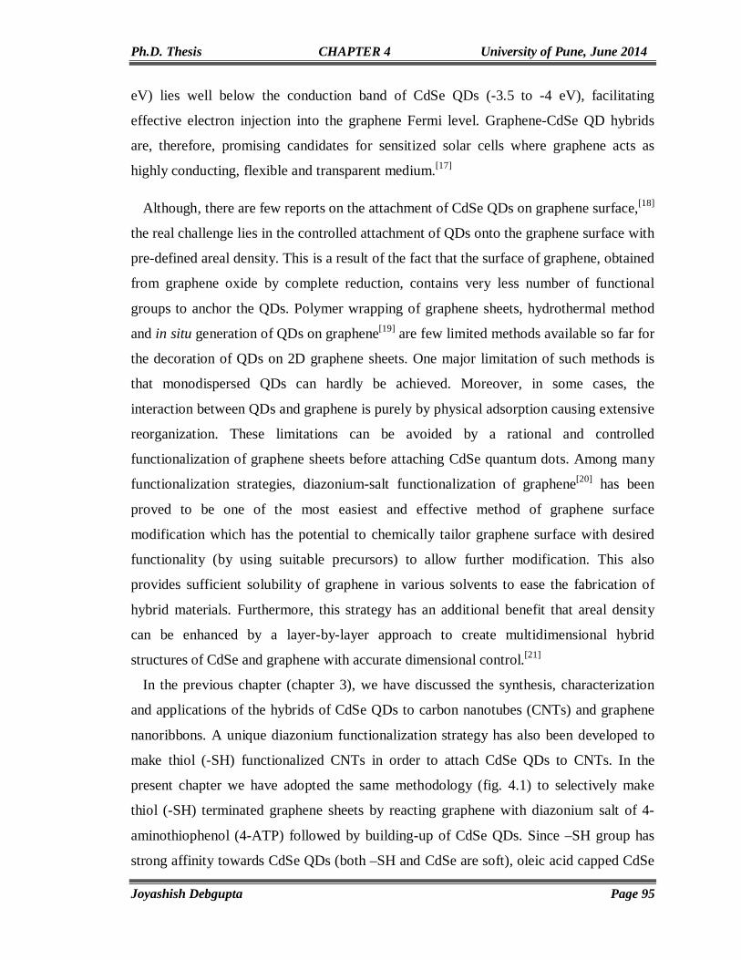
Ph.D. Thesis CHAPTER 4 University of Pune, June 2014
Joyashish Debgupta Page 95
eV) lies well below the conduction band of CdSe QDs (-3.5 to -4 eV), facilitating
effective electron injection into the graphene Fermi level. Graphene-CdSe QD hybrids
are, therefore, promising candidates for sensitized solar cells where graphene acts as
highly conducting, flexible and transparent medium.[17]
Although, there are few reports on the attachment of CdSe QDs on graphene surface,[18]
the real challenge lies in the controlled attachment of QDs onto the graphene surface with
pre-defined areal density. This is a result of the fact that the surface of graphene, obtained
from graphene oxide by complete reduction, contains very less number of functional
groups to anchor the QDs. Polymer wrapping of graphene sheets, hydrothermal method
and in situ generation of QDs on graphene[19] are few limited methods available so far for
the decoration of QDs on 2D graphene sheets. One major limitation of such methods is
that monodispersed QDs can hardly be achieved. Moreover, in some cases, the
interaction between QDs and graphene is purely by physical adsorption causing extensive
reorganization. These limitations can be avoided by a rational and controlled
functionalization of graphene sheets before attaching CdSe quantum dots. Among many
functionalization strategies, diazonium-salt functionalization of graphene[20] has been
proved to be one of the most easiest and effective method of graphene surface
modification which has the potential to chemically tailor graphene surface with desired
functionality (by using suitable precursors) to allow further modification. This also
provides sufficient solubility of graphene in various solvents to ease the fabrication of
hybrid materials. Furthermore, this strategy has an additional benefit that areal density
can be enhanced by a layer-by-layer approach to create multidimensional hybrid
structures of CdSe and graphene with accurate dimensional control.[21]
In the previous chapter (chapter 3), we have discussed the synthesis, characterization
and applications of the hybrids of CdSe QDs to carbon nanotubes (CNTs) and graphene
nanoribbons. A unique diazonium functionalization strategy has also been developed to
make thiol (-SH) functionalized CNTs in order to attach CdSe QDs to CNTs. In the
present chapter we have adopted the same methodology (fig. 4.1) to selectively make
thiol (-SH) terminated graphene sheets by reacting graphene with diazonium salt of 4-
aminothiophenol (4-ATP) followed by building-up of CdSe QDs. Since –SH group has
strong affinity towards CdSe QDs (both –SH and CdSe are soft), oleic acid capped CdSe
Ph.D. Thesis CHAPTER 4 University of Pune, June 2014
Joyashish Debgupta Page 96
QDs with pre-defined sizes have been effectively exchanged with these thiolated
graphene by mixing in solution, to orchestrate CdSe-Graphene hybrids. These hybrids are
characterized using FTIR, UV-VIS, Photoluminescence (PL), TEM and cyclic
voltammetry.
Figure 4.1. A schematic representation of the synthetic strategy of RGO and –SH terminated RGO followed by CdSe attachment through chemical exchange with oleic acid.
On the other hand, in spite of several reports on graphene-CdSe QD hybrids,[17], [22]
the basic understanding of relaxation of excited CdSe QDs in presence of graphene is not
clear. Similarly, how the “edge effect” of graphene impacts the carriers in CdSe QDs or
vice versa, also remains a question. Bruset al.[23] have reported that the excited CdSe QDs
decays by energy transfer (by the celebrated “Förster Resonant Energy Transfer
mechanism”) to pristine graphene and also have explored the possibility of electron
transfer. According to them electron transfer can predominate over energy transfer when
there is a strong chemical interaction between CdSe QDs and graphene. But,
unfortunately there has been no experimental report to date which can prove this
important hypothesis. A closely related report by Bang et al. shows an interesting thiol
modification of C60, which is a structural analogue of graphene (C60 is topologically
Ph.D. Thesis CHAPTER 4 University of Pune, June 2014
Joyashish Debgupta Page 97
linked with graphene) explaining both its ability to anchor CdSe QDs effectively and also
the higher efficiency of exciton generation.[24] Accordingly, in this chapter steady state
and time resolved photoluminescence (PL) measurements have been employed to
confirm the electron transfer process in CdSe-RGO-SH hybrid systems and this is also
supported by Raman analysis of the CdSe-RGO-SH hybrids. The rate of charge transfer
has been shown to increase with increase in particle size. Photoconductivity properties of
the graphene-QD device under illumination have also been examined and it is to be noted
that 2-3 fold increase in the photocurrent is found in this composite device in presence of
1.5 AM solar simulated light. The enhancement of photocurrent in this hybrid device is
found to be suitable for potential applications in optoelectronic and solar cell systems.
The results of the present study are relevant for the effective utilization of the hybrids for
solar cells and other photon energy harvesting systems because the understanding of
fundamental charge transfer process to graphene is directly related to the photon to
current conversion efficiency of such devices. More significantly, a fundamental
understanding of the size dependent efficiency of QDs in transferring electrons to
graphene is extremely valuable for designing better solar cells employing colloidal QDs
and graphene or its derivatives.
4.2. Experimental Section 4.2.1. Materials
Graphite powder, Sodium dodecylsulphonate (SDS), NaBH4 and 4-aminothiophenol were
purchased from Aldrich and used as received. H2SO4 (98%), HNO3 (63%), HCl (38%),
NaNO2, H2O2 were received from Thomas Baker and used without any further
purification. PTFE filter paper was obtained from Rankem. MilliQ water (DI water) was
used for all purposes unless otherwise stated. Spectroscopic grade toluene and DMF were
obtained from MERCK. Cadmium oxide (CdO), trioctyl phosphine (TOP) and 1-
octadecene were purchased from Aldrich and used as received. Se powder, hexane and
ethanol (99.9%) of analytical reagent grade were purchased from Thomas Baker. Oleic
acid was purchased from Rankem and used without further purification.
4.2.2. Reduction of surfactant wrapped graphene oxide (GO) using NaBH4
Ph.D. Thesis CHAPTER 4 University of Pune, June 2014
Joyashish Debgupta Page 98
GO was prepared separately from powder graphite adopting the Hummers and Offman
method. [25-26] 0.1g Graphene Oxide (GO) was suspended in water using sonication for 15
min followed by reduction with NaBH4 (1:3 wt. ratio) for 12 h to obtain chemically
converted graphene (CCG) or reduced graphene oxide (RGO).
4.2.3. Preparation of thiol (-SH) functionalized graphene (RGO-SH)
A diazonium salt of 4-aminothiophenol (4-ATP) was prepared by mixing 70 mg 4-ATP
with 200 mg NaNO2 in 40 mL distilled water at 0-5°C followed by the addition of 3 mL
6 M HCl solution (ice cold) slowly to the above mixture. A gradual change of the
solution color (transparent) to pale yellow indicated the formation of diazonium salt. The
mixture was then slowly (and with constant stirring) added to the RGO suspension (at 0-
5°C) and allowed to stir for 2 h at 0-5°C and another 2 h at room temperature (30°C).
Subsequently, the reaction mixture was filtered, washed with DI water and re-suspended
in DMF to remove the SDS surfactant and excess unreacted 4-ATP molecules. The
suspension was finally filtered and washed to get –Ph-SH functionalized RGO -SH.
4.2.4. Exchange of oleic acid capped CdSe QDs with RGO-SH)
Oleic acid capped CdSe NPs (CdSe-OA, Chapter 2, section 2.2) (concentration of CdSe
suspension was maintained by fixing the first excitonic peak intensity at 0.1 optical
density throughout all our experiments) were exchanged by mixing the DMF suspension
of RGO-SH (12.7 mg ml-1) with toluene soluble CdSe-OA.
4.3. Structural and Morphological Characterization 4.3.1. UV-Vis absorption
Optical absorption spectra were taken at room temperature by a UV-Vis
spectrophotometer (SHIMADZU).
4.3.2. Photoluminescence Spectroscopy
Room temperature steady state photoluminescence spectra were recorded by a
Fluoromax-P (HORIBA JOBIN YVON) spectrophotometer. Photoluminescence quantum
yields (QY) for CdSe QDs were obtained by comparison with reference dye (rhodamine
6G in water), using the following equation:
QYs = (Fs× Ar × ns2 × QYr) / (Fr × As × nr
2)……………………………..(1)

Ph.D. Thesis CHAPTER 4 University of Pune, June 2014
Joyashish Debgupta Page 99
where Fs and Fr are the integrated fluorescence emission of the sample and the reference
respectively. As and Ar are the absorbance at the excitation wavelength of the sample and
the reference and QYs and QYr are the quantum yields of the sample and the reference
(QYr = 95%).[27] The refractive indices of the solvents used for the preparation of the
sample (in toluene) and reference (in water) are given by ns (1.49) and nr (1.33)
respectively. The values of Fs and Fr were determined from the photoluminescence
spectra corrected for the instrumental response, by integrating the emission intensity over
the desired spectral range. Only the band edge luminescence peak was integrated (any
other luminescence bands, such as defect associated luminescence or solvent
fluorescence were discarded as background).
4.3.3. Time correlated single photon counting (TCSPC) measurement
For the time correlated single photon counting (TCSPC) measurements, the samples were
excited at 375 nm using a nano-second diode laser (IBH Nanoled) in an IBH Fluorocube
apparatus. The typical full width at half-maximum (FWHM) of the system response using
a liquid scatter was about 300 ps. The repetition rate was 1 MHz.The fluorescence decays
were analyzed using IBH DAS6 software. The following equation was used to analyze
the experimental time resolved fluorescence decays,[28]
)exp()(i
n
ii
tbtPτ
α −+= ∑ …………………(2)
here, n is a number of discrete emissive species, b is a baseline correction (“dc” offset),
and αi and τi are pre-exponential factors and excited-state fluorescence lifetimes
associated with the ith component, respectively. For multi-exponential decays the average
lifetime,⟨τ⟩, was calculated from the following equation,[29]
∑=
>=<n
iiia
1
ττ ……………………..(3)
Where ∑= iiia αα / and ia is contribution of the decay component.
Ph.D. Thesis CHAPTER 4 University of Pune, June 2014
Joyashish Debgupta Page 100
Other characterization details like FTIR, SEM, EDAX, XPS, Contact angle measurement,
TGA and electrochemical techniques have already been discussed in Chapter 2 (section
2.2) and Chapter 3 (section 3.2)
4.4. Results and Discussion 4.4.1. FTIR analysis
FTIR spectra were recorded in order to confirm the successful grafting of –PhSH group.
Accordingly, fig. 4.2 shows comparative FTIR spectra of reduced Graphene oxide
(RGO), 4-aminothiophenol (4-ATP) and thiol modified graphene. Less intense
characteristic peak for –SH group (~2530 cm-1) is observed in thiol modified graphene.
The same peak appears at 2569 cm-1 (very weak at 2569 cm-1) in case of 4-ATP
molecule. However, the peak for thiol is rather broad. This is in accordance with the
information available in literature that the –SH peak is very difficult to be observed in
FTIR and moreover, vibrational peaks of graphene (specially remaining –COOH group)
are so strong that those can mask the actual –SH peak. The presence of –SH group hence
confirms the successful grafting of –PhSH group on graphene surface. It also proves that
–SH group exists mostly as –SH moiety and not any other form. The spectrum for 4-ATP
molecule however shows, (other than –SH peak) several peaks corresponding to =C-H
deformation of benzene ring (825 cm-1), C=C in plane vibration (1625, 1497 cm-1),
aromatic =C-H stretching (3026 cm-1) and finally the N-H stretching (3375 cm-1) of
charged aromatic amine group.[30] The absence of N-H stretching peak as well as the
presence of both S-H and C-H stretching peaks ensure proper functionalization,
presumably with the loss of –NH2 group as molecular N2 during aromatic electrophilic
reaction (C-C bond formation) on the graphene surface.

Ph.D. Thesis CHAPTER 4 University of Pune, June 2014
Joyashish Debgupta Page 101
Figure 4.2. Superimposed FTIR spectra of RGO (RGO), -SH grafted RGO (RGO-SH) and 4-ATP; Stretching peak of –SH group is seen at 2530 cm-1 for RGO-SH and at 2569 cm-1 for 4-ATP molecule (sky blue region); N-H stretching vibration disappears after diazotization (yellow region). 4.4.2. Scanning Electron Microscopy and EDAX mapping
After confirming the presence of –SH group on RGO surface, SEM elemental mapping
(EDAX) has been employed in order to see the distribution or the grafting density of –SH
groups in RGO-SH. Accordingly, fig. 4.3 shows the elemental mapping of the thiolated
graphene revealing an almost complete coverage of S (or –SH group). From the
quantitative analysis of EDAX, ~4 wt% sulphur (S) has been estimated for the case of 1:1
wt% of graphene to 4-ATP. This approximately indicates about ~1018 to1020 number of
–SH units per gram of graphene surface.

Ph.D. Thesis CHAPTER 4 University of Pune, June 2014
Joyashish Debgupta Page 102
Figure 4.3. SEM image of a portion of RGO-SH and the EDAX maps of C, S, O elements in the hybrid material; S-shows a uniform distribution over the material indicating similar functionalization throughout the RGO surface; below is the EDAX plot of RGO-SH showing the presence of S.
4.4.3. TGA analysis
In order to further confirm the chemical bonding between –PhSH group and RGO
surface, several thermogravimetric experiments have been carried out. Accordingly, fig.
4.4 shows a comparison of the thermograms of pure RGO, pure 4-ATP molecule, RGO-
SH (chemically functionalized RGO) and a physical mixture of RGO and 4-ATP
(RGO+4-ATP) in nitrogen. It can be observed from the thermograms that the physical
mixture shows same decomposition profile as that of pure 4-ATP molecule except the
remaining mass at 900 °C. The higher residual mass in case of the physical mixture as
compared to that of pure 4-ATP is due to the presence of graphene. This clearly suggests
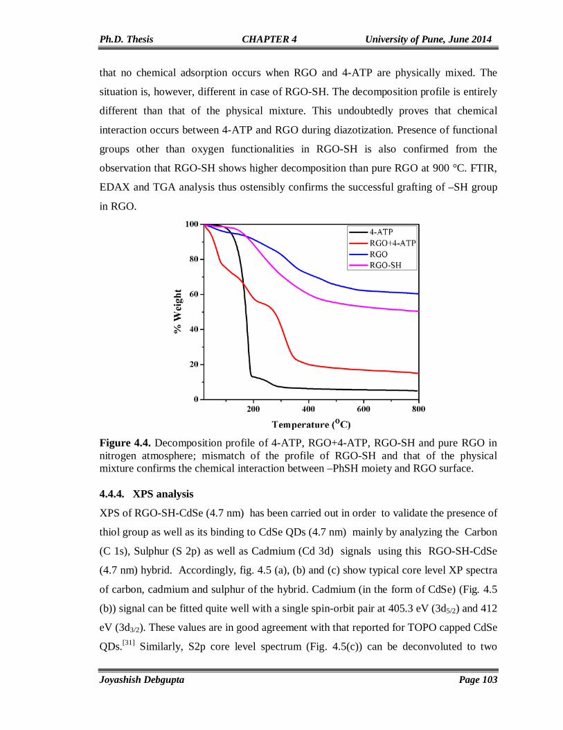
Ph.D. Thesis CHAPTER 4 University of Pune, June 2014
Joyashish Debgupta Page 103
that no chemical adsorption occurs when RGO and 4-ATP are physically mixed. The
situation is, however, different in case of RGO-SH. The decomposition profile is entirely
different than that of the physical mixture. This undoubtedly proves that chemical
interaction occurs between 4-ATP and RGO during diazotization. Presence of functional
groups other than oxygen functionalities in RGO-SH is also confirmed from the
observation that RGO-SH shows higher decomposition than pure RGO at 900 °C. FTIR,
EDAX and TGA analysis thus ostensibly confirms the successful grafting of –SH group
in RGO.
Figure 4.4. Decomposition profile of 4-ATP, RGO+4-ATP, RGO-SH and pure RGO in nitrogen atmosphere; mismatch of the profile of RGO-SH and that of the physical mixture confirms the chemical interaction between –PhSH moiety and RGO surface. 4.4.4. XPS analysis
XPS of RGO-SH-CdSe (4.7 nm) has been carried out in order to validate the presence of
thiol group as well as its binding to CdSe QDs (4.7 nm) mainly by analyzing the Carbon
(C 1s), Sulphur (S 2p) as well as Cadmium (Cd 3d) signals using this RGO-SH-CdSe
(4.7 nm) hybrid. Accordingly, fig. 4.5 (a), (b) and (c) show typical core level XP spectra
of carbon, cadmium and sulphur of the hybrid. Cadmium (in the form of CdSe) (Fig. 4.5
(b)) signal can be fitted quite well with a single spin-orbit pair at 405.3 eV (3d5/2) and 412
eV (3d3/2). These values are in good agreement with that reported for TOPO capped CdSe
QDs.[31] Similarly, S2p core level spectrum (Fig. 4.5(c)) can be deconvoluted to two

Ph.D. Thesis CHAPTER 4 University of Pune, June 2014
Joyashish Debgupta Page 104
peaks at 163.4 eV and 166.7 eV respectively. The first peak (163.4 eV) corresponds to
the S atoms of –PhSH groups, bonded to CdSe QDs while the peak at higher binding
energy (166.7 eV) is associated with the presence of some amount of S-atoms at higher
oxidation state (S6+), formed during the sample preparation and exposure to X-rays as has
been observed previously.[32] Binding to CdSe renders the S-atom (of –SH group) more
electronegative and hence the consequent blue shift of the binding energy of sulphur as
compared to S in normal –SH group (161-162 eV). This value of binding energy (B.E)
(for CdSe-thiol bonding) is in excellent agreement with the reported B.E value for S 2p
signal in case of self-assembled monolayers of alkanethiols, aromatic thiols as well as
alkanethiol capped silver nanoparticles.[33-35] It reveals that in the homogeneous mixture
of CdSe QDs (in toluene) and RGO-SH (in DMF), and CdSe QDs are chemically bonded
to RGO-SH surface due to ligand exchange between thiol group and oleic acid. As no
peak for carbon-sulphur binding (164 eV according to literature [36]) is observed in the
spectrum, 4-ATP molecule is expected to be bonded through C-C linkage to graphene
and not through C-S bond. C1s (Fig.4.5 (a)) signal also corroborates well with this
explanation. C1s signal can be de-convoluted to 4 different peaks. The low B.E peak at
284.1 eV corresponds to sp2 carbons from the graphene (RGO-SH) surface and the peak
at 284.9 eV is due to sp3 carbons resulting from covalent functionalization on graphene
surface. Higher B.E peaks at 286 eV and 288 eV indicate the attachment of carbons to
more electronegative elements like oxygen and sulphur. However, the intensity and the
area of this high B.E peak are very small as compared to rest of the peaks which suggests
that the amount of higher oxidation sulphur species (S6+) is very small.

Ph.D. Thesis CHAPTER 4 University of Pune, June 2014
Joyashish Debgupta Page 105
Figure 4.5. Core level XPspectra of (a) Carbon (C1s), (b) Cadmium (Cd 3d) and (c)
Sulphur (S-2p) from RGO-SH-CdSe (4.7 nm) hybrid.
4.4.5. Cyclic voltammetry
Cyclic voltammetry has been employed to characterize the RGO before and after –SH
grafting. Ferrocene methanol has been used as a redox probe to understand the
conductivity property of RGO before and after –SH grafting. Accordingly, distinct redox
peaks, for the oxidation and reduction of ferrocene methanol (fig. 4.6), are observed in
case of RGO which is a good electron carrier. Interestingly, when the same coating is
subjected to thiol functionalization for 2 h, the current for the redox peaks are found to
decrease. This is because the surface of the RGO gets modified with –Ph-SH groups,
which in turn hinders the diffusion of ferrocene methanol molecules towards the RGO
surface and as a result the current drops. Integrating the area of the oxidation peak gives
~10-7 molcm-2 surface coverage of –PhSH group on the surface of RGO.
Figure 4.6. Cyclic voltammogram of RGO coated on Pt electrode (2 mm dia) in 0.5 mM ferrocenemethanol containing 0.1 M KCl aqueous solution, Ag/AgCl was used as

Ph.D. Thesis CHAPTER 4 University of Pune, June 2014
Joyashish Debgupta Page 106
reference electrode and Pt-foil as counter electrode, Scan rate was 10 mVs-1; For comparison CV of Pt disk also has been shown. 4.4.6. Impedance measurement
Impedance measurement has been carried out to support the result obtained from cyclic
voltammetry. Accordingly, fig. 4.7 (a) shows Nyquist plotsof RGO and RGO-SH under
similar conditions of CV using ferrocenemethanol as the redox probe. The diameter of
the high frequency semicircle which is a measure of charge transfer resistance is found to
increase after –SH grafting. Moreover, diffusion coefficient of ferrocene methanol,
obtained from the low frequency straight line portion (by plotting modulus of Z vs. ɷ -1/2in
Fig. 4.7 (b)), suggests the poor diffusion of the molecules to the electrode surface (RGO
here) due to the presence of thiolgroup (pinning). The thiol groups impede the incoming
flux of ferrocene methanol molecules to the RGO surface and thereby results in the
higher charge transfer resistance.[37]
Figure 4.7. (a) Nyquist plot for the same system before and after –SH functionalization; The Rct increases after functionalization, (c) ɷ-1/2 vs mod. Z plot from the low frequency part of the Nyquist plot for the calculation of diffusion coefficient of the ferrocene methanol. 4.4.7. Contact angle measurement
Contact angle of any liquid on any substrate is an important parameter which is very
sensitive to surface functionality provided that the microstructure remains same. Hence, a
systematic analysis of the water contact angle change has been carried out on RGO and
RGO-SH surfaces in order to understand the change due to –SH grafting. Accordingly,

Ph.D. Thesis CHAPTER 4 University of Pune, June 2014
Joyashish Debgupta Page 107
substrate change from pristine graphene to RGO-SH shows (fig. 4.8) increased
hydrophobic character due to –PhSH grafting (water contact angle increases from 82° to
91° after functionalization). Surface energy of RGO has been calculated, before and after
–PhSH grafting, using Ownes-Wendt method suggesting an increase in surface energy
from 33.1 to 40.3 mJm-2) after functionalization.[38] However, the polar or non-dispersive
component of the surface energy decreases (5.5 to 0.6 mJm-2) after functionalization with
a concomitant increase in dispersive or non-polar component (27.6 to 39.8 mJm-2).
Figure 4.8. Water contact angle on RGO and RGO-SH surface; film of each sample was made by electrophoretic deposition (solvent N-methyl pyrrolidone for RGO and Dimethylformamide for RGO-SH) on clean FTO plates and dried at 100°C under vacuum for 8 h to get a smooth surface so as to minimize errors due to surface roughness. 4.4.8. Micro Raman
Raman mapping (fig. 4.9) has been used extensively to characterize the functionalized
RGO and the hybrids. More specifically, three different sizes of CdSe QDs have been
chosen, (namely 3.8 nm, 4 nm and 4.9 nm) and their capping agents were exchanged with
the –SH functionalized graphene (RGO-SH) hybrid. As has been indicated in fig. 4.9(a),
all the three hybrids show two characteristics phonon modes of vibrations on excitation-
one at 1333.1 cm-1 and another at 1582.8 cm-1. The first one is identified as the D-band or
defect induced band which appears due to in plane longitudinal phonon vibration or
breathing mode of k-point phonons of A1g symmetry and the later one is the G-band or
graphitic band arising due to E2g phonon mode for sp2 carbon network of graphene plane.
However, when compared with pristine RGO without any thiol functionalization and
CdSe QDs decoration, there is ~13 cm-1 shift of both D as well as G- bands towards

Ph.D. Thesis CHAPTER 4 University of Pune, June 2014
Joyashish Debgupta Page 108
lower wavenumber or energy (fig. 4.9(b)).This red shift (equivalent to 1.6 meV) implies
softening of phonons of RGO due to electron enrichment on graphene because of charge
transfer to graphene.[39] A similar effect has been observed in case of molecular doping in
graphene in presence of an electron donor like tetrathiafulvalene (TTF)[32] where a shift of
~10 cm-1 has led to a doping (electron) concentration of ~1012 cm-2 for 0.1 M TTF in
graphene.
Figure 4.9. (a)Micro Raman spectra of CdSe-RGO-SH hybrids with 514 nm Ar+ laser using 50x objective, (b) enlarged portion of D and G bands of RGO showing charge transfer from CdSe to RGO, (c) variation of peak position of CdSe QDs with particle size.
The excitation source 514 nm laser has sufficient energy (2.41 eV) to excite the valence
band electrons of CdSe QDs, the work function of graphene (-4.5 eV) being favorable
with the conduction band positions of these QDs (-4.17 to -4.38 eV for 3.8 nm to 4.9 nm
particles), excited electrons can be transferred to graphene and thereby rendering the
graphene surface electron rich. This consequently results in a red shift in the D and G-
band positions of the graphene. Interestingly, ID to IG ratio (1.01 in this case) remains the
same both for pristine RGO as well as for functionalized and CdSe decorated RGO
confirming that the nature and amount of defect remains the same before and after the

Ph.D. Thesis CHAPTER 4 University of Pune, June 2014
Joyashish Debgupta Page 109
functionalization. On the other hand, the appearance of 2D band, which is the overtone
band of D-band, in all samples, indicates that the number of layers is not disturbed
significantly due to functionalization.[20] A typical crystallite size of ~16.6 nm has been
estimated from the ID/IG ratio, which basically represents the distance between two
successive defect points. Other than the D-and G-bands, the Raman spectra of the hybrid
materials also bear the feature of CdSe QDs in the 100 – 500 cm-1 region. The peak at
201-202 cm-1 is attributed to the longitudinal optical (LO) phonon mode of CdSe and that
at 400-405 cm-1 is the overtone of LO mode which is termed as CdSe 2LO. As Fig.4.9(c)
suggests, the LO peak shows a slow red shift with the decrease in particle size, in
accordance with the previous report.[40] the appearance of LO peak within 201-202 cm-1
as compared to 210 cm-1 for bulk CdSe, suggests the invariance of the size and shape for
the attached QDs.[40]
4.4.9. Transmission Electron Microscopy
TEM analysis has been carried out in order to see the distribution and particle size of
QDs on RGO-SH surface. Accordingly, fig. 4.10(a-d) displays low and high resolution
(HRTEM) images of f-RGO and RGO-SH-CdSe QD (4.7 nm) hybrids respectively.
Images for the hybrids were taken of the samples containing 0.268 mg/mL of RGO-SH.
Interestingly, low magnification image shows complete coverage of the QDs on RGO-SH
(fig.4.10(b)) as compared to only RGO-SH (fig.4.10(a)) in which case no CdSe QD is
visible. After the exchange with the thiol groups on RGO, CdSe QDs interestingly form
an almost complete monolayer on RGO at this concentration of RGO-SH. The FFT in the
inset of fig. 4.10(d) indicates the formation of cubic CdSe and more significantly, the d-
spacing (2.9 Å) matches well with that of literature report (zinc blende phase, JCPDS card
no.19-0191).
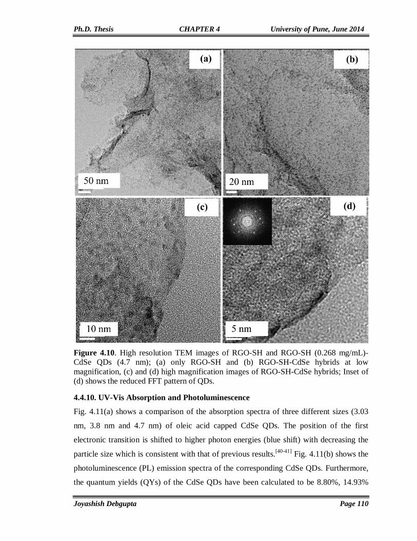
Ph.D. Thesis CHAPTER 4 University of Pune, June 2014
Joyashish Debgupta Page 110
Figure 4.10. High resolution TEM images of RGO-SH and RGO-SH (0.268 mg/mL)-CdSe QDs (4.7 nm); (a) only RGO-SH and (b) RGO-SH-CdSe hybrids at low magnification, (c) and (d) high magnification images of RGO-SH-CdSe hybrids; Inset of (d) shows the reduced FFT pattern of QDs.
4.4.10. UV-Vis Absorption and Photoluminescence
Fig. 4.11(a) shows a comparison of the absorption spectra of three different sizes (3.03
nm, 3.8 nm and 4.7 nm) of oleic acid capped CdSe QDs. The position of the first
electronic transition is shifted to higher photon energies (blue shift) with decreasing the
particle size which is consistent with that of previous results.[40-41] Fig. 4.11(b) shows the
photoluminescence (PL) emission spectra of the corresponding CdSe QDs. Furthermore,
the quantum yields (QYs) of the CdSe QDs have been calculated to be 8.80%, 14.93%
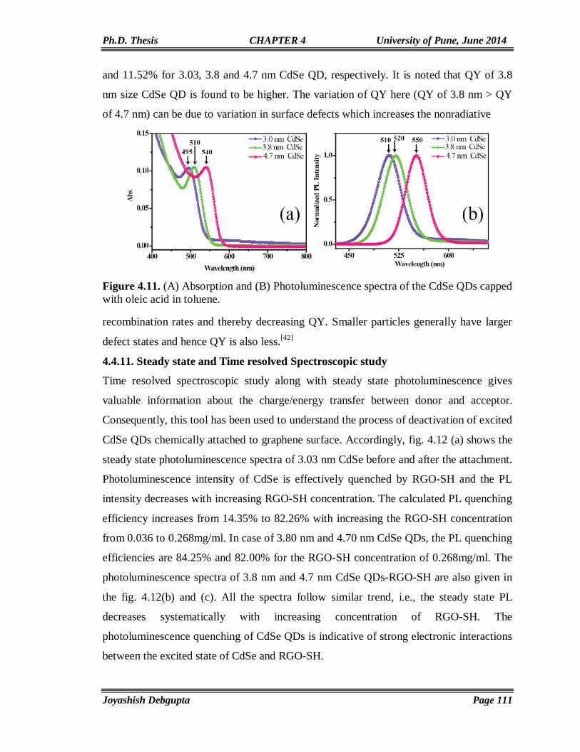
Ph.D. Thesis CHAPTER 4 University of Pune, June 2014
Joyashish Debgupta Page 111
and 11.52% for 3.03, 3.8 and 4.7 nm CdSe QD, respectively. It is noted that QY of 3.8
nm size CdSe QD is found to be higher. The variation of QY here (QY of 3.8 nm > QY
of 4.7 nm) can be due to variation in surface defects which increases the nonradiative
Figure 4.11. (A) Absorption and (B) Photoluminescence spectra of the CdSe QDs capped with oleic acid in toluene.
recombination rates and thereby decreasing QY. Smaller particles generally have larger
defect states and hence QY is also less.[42]
4.4.11. Steady state and Time resolved Spectroscopic study
Time resolved spectroscopic study along with steady state photoluminescence gives
valuable information about the charge/energy transfer between donor and acceptor.
Consequently, this tool has been used to understand the process of deactivation of excited
CdSe QDs chemically attached to graphene surface. Accordingly, fig. 4.12 (a) shows the
steady state photoluminescence spectra of 3.03 nm CdSe before and after the attachment.
Photoluminescence intensity of CdSe is effectively quenched by RGO-SH and the PL
intensity decreases with increasing RGO-SH concentration. The calculated PL quenching
efficiency increases from 14.35% to 82.26% with increasing the RGO-SH concentration
from 0.036 to 0.268mg/ml. In case of 3.80 nm and 4.70 nm CdSe QDs, the PL quenching
efficiencies are 84.25% and 82.00% for the RGO-SH concentration of 0.268mg/ml. The
photoluminescence spectra of 3.8 nm and 4.7 nm CdSe QDs-RGO-SH are also given in
the fig. 4.12(b) and (c). All the spectra follow similar trend, i.e., the steady state PL
decreases systematically with increasing concentration of RGO-SH. The
photoluminescence quenching of CdSe QDs is indicative of strong electronic interactions
between the excited state of CdSe and RGO-SH.

Ph.D. Thesis CHAPTER 4 University of Pune, June 2014
Joyashish Debgupta Page 112
Figure 4.12. Steady state photoluminescence quenching with incremental amount of RGO-SH; (a) CdSe QDs of 3.0 nm, (b) CdSe QDs of 3.8 nm and (c) CdSe QDs of 4.7 nm.
To confirm the energy/electron transfer process from QD to graphene, a time
resolved fluorescence study has further been performed which is indeed, more sensitive
than PL quenching. Accordingly, fig. 4.13(a) shows the photoluminescence decay curves
of 3.03 nm CdSe as a function of increasing concentration of RGO-SH at the excitation
and emission wavelength of 375 nm and 510 nm, respectively. All the decay curves are
fitted with tri-exponential functions. The decay components of the pure 3.03 nm CdSe
QD are 0.76 ns (58.4%), 7.70 ns (27.4%) and 39.29 ns (14.2%) and the average decay
time is 8.13 ns according to eq.3. In presence of highest concentration of RGO-SH (0.268
mg/ml), the corresponding components are 0.57 ns (74.5%), 6.48 ns (18.2%) and 38.49
ns (7.3%) and the average decay time is 4.41 ns. The fluorescence decay time of CdSe
QDs decreases with the increasing concentration of RGO-SH which is consistent with the
fluorescence results. With increasing the RGO-SH concentration, the fast component (τ1)
decreases from 0.76 ns to 0.57 ns over the RGO-SH concentration range of 0.036-0.268

Ph.D. Thesis CHAPTER 4 University of Pune, June 2014
Joyashish Debgupta Page 113
mg/ml but slow components (τ2 and τ3) decrease negligibly small (Table 4.1). The
contribution of the fast component increases from 58.8% to 74.5% respectively while the
contribution of slow components decreases from 27.7% to 18.2% and 14.2% to 7.3%
only.
Figure 4.13. Time resolve spectra of CdSe and CdSe- RGO-SH at the excitation wavelength of 375 nm; (a) 3.0 nm CdSe QDs, (b) 3.8 nm CdSe QDs and (c) 4.7 nm CdSe QDs.
Actually, the fast component is responsible for the photo-excited electron
transfer[22] and the slow component mainly arises from the free CdSe in the solution.
With the increase of RGO-SH concentration, the number of free CdSe QDs is expected to
diminish in the solution and as a result, the contribution of the slow decay components
decreases. For the other two QDs, 3.8 nm and 4.7 nm CdSe, similar results are observed.
The corresponding decay profiles and decay parameters are given in fig. 4.13(b), (c) and
Table 4.2 and 4.3 respectively. The fast components decrease from 0.91ns to 0.42 ns and
0.77 ns to 0.49 ns for the 3.80 nm and 4.70 nm CdSe QDs, respectively. Therefore, the
decrease of fast component and increase of fast decay component contribution in CdSe-
RGO-SH hybrid implies the photoluminescence quenching of CdSe QDs by RGO-SH
through photo-excited electron transfer from CdSe QDs to RGO-SH. We have calculated
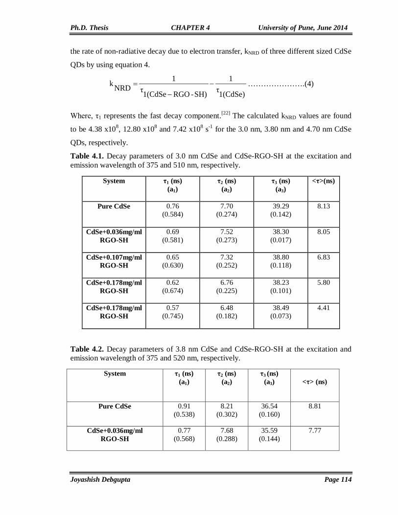
Ph.D. Thesis CHAPTER 4 University of Pune, June 2014
Joyashish Debgupta Page 114
the rate of non-radiative decay due to electron transfer, kNRD of three different sized CdSe
QDs by using equation 4.
1(CdSe)τ1
SH)-RGO1(CdSeτ1
NRDk −−
= ………………….(4)
Where, τ1 represents the fast decay component.[22] The calculated kNRD values are found
to be 4.38 x10⁸, 12.80 x10⁸ and 7.42 x10⁸ s-1 for the 3.0 nm, 3.80 nm and 4.70 nm CdSe
QDs, respectively.
Table 4.1. Decay parameters of 3.0 nm CdSe and CdSe-RGO-SH at the excitation and emission wavelength of 375 and 510 nm, respectively.
System
τ1 (ns) (a1)
τ2 (ns) (a2)
τ3 (ns) (a3)
<τ>(ns)
Pure CdSe
0.76 (0.584)
7.70 (0.274)
39.29 (0.142)
8.13
CdSe+0.036mg/ml RGO-SH
0.69 (0.581)
7.52 (0.273)
38.30 (0.017)
8.05
CdSe+0.107mg/ml RGO-SH
0.65 (0.630)
7.32 (0.252)
38.80 (0.118)
6.83
CdSe+0.178mg/ml RGO-SH
0.62 (0.674)
6.76 (0.225)
38.23 (0.101)
5.80
CdSe+0.178mg/ml RGO-SH
0.57 (0.745)
6.48 (0.182)
38.49 (0.073)
4.41
Table 4.2. Decay parameters of 3.8 nm CdSe and CdSe-RGO-SH at the excitation and emission wavelength of 375 and 520 nm, respectively.
System τ1 (ns) (a1)
τ2 (ns) (a2)
τ3 (ns) (a3)
<τ> (ns)
Pure CdSe 0.91 (0.538)
8.21 (0.302)
36.54 (0.160)
8.81
CdSe+0.036mg/ml RGO-SH
0.77 (0.568)
7.68 (0.288)
35.59 (0.144)
7.77

Ph.D. Thesis CHAPTER 4 University of Pune, June 2014
Joyashish Debgupta Page 115
CdSe+0.107mg/ml RGO-SH
0.65 (0.618)
6.86 (0.260)
33.9 (0.122)
6.27
CdSe+0.178mg/ml RGO-SH
0.63 (0.645)
6.39 (0.250)
32.46 (0.105)
5.41
CdSe+0.268mg/ml RGO-SH
0.42 (0.780)
5.37 (0.163)
32.31 (0.057)
3.04
Table 4.3. Decay parameters of 4.7 nm CdSe and CdSe-RGO-SH at the excitation and emission wavelength of 375 and 550 nm, respectively.
System τ1 (ns) (a1)
τ2 (ns) (a2)
τ3 (ns) (a3)
<τ> (ns)
Pure CdSe 0.77 (0.585)
7.73 (0.297)
30.85 (0.118)
6.39
CdSe+0.036mg/ml RGO-SH
0.67 (0.568)
7.16 (0.288)
29.57 (0.144)
5.63
CdSe+0.107mg/ml RGO-SH
0.60 (0.640)
6.72 (0.262)
29.19 (0.098)
5.00
CdSe+0.178mg/ml RGO-SH
0.58 (0.698)
6.17 (0.229)
28.49 (0.073)
3.89
CdSe+0.268mg/ml
RGO-SH
0.49 (0.764)
5.69 (0.184)
29.20 (0.052)
2.94
This nonradiative decay rate is due to electron transfer process. It is found that 3.80 nm
CdSe QD exhibits highest electron transfer rate, which may be due to the higher QY (less
number of non-emissive trap states favors the electron transfer rate) and better electronic
interaction with the RGO-SH (the energy gap between conduction band of 3.8 nm CdSe
QD [-3.3 eV] and the Fermi level of graphene [-4.5 eV]). Table 4.4 clearly shows that the
non-radiative rate constant, is for the electron transfer from CdSe to RGO-SH.

Ph.D. Thesis CHAPTER 4 University of Pune, June 2014
Joyashish Debgupta Page 116
Table 4.4. Rate constant of electron transfer from CdSe QDs to RGO-SH as a function of QD size.
CdSe QD τ1(RGO-SH-CdSe) τ1(CdSe) Rate constant (ns-1)
3.0 nm 0.42 0.76 0.438
3.8 nm 0.57 0.91 1.280
4.7 nm 0.49 0.71 0.742
Table 4.5. Energy band positions of CdSe QDs with respect to vacuum.
Size of
CdSe QD (nm)
HOMO (eV)
vs vacuum
LUMO (eV)
vs vacuum
3.0 -6.24 -3.48
3.8 -6.15 -3.30
4.7 -5.95 -3.40
It is also predicted that the enhancement of the electron transfer (and not energy
transfer) is observed due to direct electronic interaction between CdSe QDs and
graphene, i.e., if the QDs are chemically bonded to the graphene surface. It is reported
that the efficiency of exciton generation increases when CdSe QDs are attached with C60
by a thiol linker.[43] Functionalization of C60 allows binding of ~110-150 C60 units to one
CdSe QDs and that leads to enhanced quenching of CdSe photoluminescence, thereby
yielding more efficient exciton generation. For example, Chaban et al.[43] also have
reported that thiol functionalization of C60 can effectively bind the CdSe QDs to
accelerate the electron transfer process from CdSe QDs to C60 LUMO level by employing
the phonon vibrations of the molecular bridge containing thiol group. In the present
study, the graphene has –SH (-PhSH group) terminated group which will replace the oleic
acid ligand on the surface of QDs and a chemical coupling occurs between CdSe and
graphene. Removal of some of the oleic acid ligand with the short thiol group (-PhSH
group) thus establishes direct linking to RGO-SH through –PhSH unit which facilitates

Ph.D. Thesis CHAPTER 4 University of Pune, June 2014
Joyashish Debgupta Page 117
the electron transfer process. Moreover, the conduction band of these QDs (Table 4.5) is
well aligned with the Fermi level of graphene (-4.5 eV) to enhance the electron transfer
from QDs to graphene upon photoexcitation. Moreover, the rate constant for the non-
radiative decay is in good agreement with that reported recently by both Kamatet al[22]
and Brus et al.[23] The distance between QDs and graphene surface is ~7 Å (calculated
using MATERIALS STUDIO package) which is in favorable position for electron
transfer from excited CdSe to graphene surface. The phenyl group of –PhSH can also
help in electron transfer most probably through its π-electrons. Molecular vibration of
this linker also assists this electron transfer. Above all, thiol group is well known to
improve photoluminescence by suppressing the defect sites, which can change the band
structure of CdTe QDs.[44] Binding of CdSe QDs to graphene surface via short molecular
linker (-PhSH) thus improves the electron transfer rate from excited CdSe to graphene
Fermi level. Table 4.5 represents the absolute band positions of the CdSe QDs studied
and these values are in excellent agreement with that reported elsewhere.[45] The variation
in rate of electron transfer for different QD sizes can be understood from the difference in
the energy gap between conduction band of CdSe and the Fermi level of graphene (-4.5
eV). The difference in energy between the conduction band of CdSe and the Fermi level
of graphene is maximum for 3.8 nm QDs (Table 4.5). This can also be understood by
considering that the electrochemical techniques probe mostly the surface of QDs. Defect
states lying on the surface of QDs, can thus alter the position of peak position in CV or
DPV and this results in shifts in band positions.
4.4.12. Photovoltaic study
A bulk heterojunction type of device has been fabricated as a proof-of-concept of the
above study. Accordingly, fig.4.14 shows the dark and photocurrent of the device
prepared by graphene-CdSe-3.03 nm QD composite system. Intrinsic graphene does not
show any photocurrent under visible light exposure. However, the asymmetric shape of
I-V curves is observed in both dark and in visible light. This could be explained since
CdSe generates excitons (electron-hole pair) on illumination and these excited electrons
are readily transferred to RGO-SH from CdSe QD because of the favorable band
alignment between the conduction band of CdSe and the Fermi level of RGO-SH so that

Ph.D. Thesis CHAPTER 4 University of Pune, June 2014
Joyashish Debgupta Page 118
the hole migrates to PEDOT:PSS (p-type material). This consequently, leads to the
enhancement in photocurrent in CdSe-RGO-SH hybrids. The observed Ilight/Idark is ~2.2 at
0.6 V for 3.03 nm CdSe while for the other two QDs, the ratio is 2.7 (for 3.8 nm) and
1.54 (4.7 nm) respectively under similar condition (fig. 4.14(a) and (b)). Indeed, the
increment in photocurrent is in accordance with the observed rate of electron transfer. A
similar trend has also been recently observed for CdTe-Graphene oxide system.[46] Thus,
these hybrids of CdSe QDs and f-RGO-SH may act as potential candidates with unique
advantages for optoelectronic devices due to high photon to current conversion.
Although further investigation is required for a detailed understanding of this hybrid
system for device applications, the design of such graphene-QD functional materials
open up new avenue in solar energy conversion.
Figure 4.14. Room temperature Photoconductivity of device comprising of CdSe (3.0 nm)-RGO-SH hybrid on FTO coated glass; The device structure and the band alignments (not to scale) of the individual component are shown in the inset; the inset optical image corresponds to the spray coated film of RGO-SH-CdSe on FTO coated glass plate; Device area is 0.56 cm-2, Bias is applied to FTO with respect to ITO.
Thus from the above discussion, it is clear that anchoring of CdSe QDs chemically to
conducting graphene surface not only provides a mean to homogeneously decorate the
Ph.D. Thesis CHAPTER 4 University of Pune, June 2014
Joyashish Debgupta Page 119
graphene, but gives a new type of hybrid material with promising applications also.
Chemical bonding enhances the rate of charge transfer from excited CdSe QD to
graphene as compared to the competing process of energy transfer. However, the
mechanism of charge transfer via the molecular linker is still unclear and it requires
additional sophisticated tools to explore the same. Moreover, there is always the
probability of restacking due to the tendency of H-bonding among –SH groups of one
RGO sheet with that of the other, which can be alleviated by proper sonication
procedures.
4.5. Conclusion
This chapter deals with the synthesis of a unique CdSe-graphene hetero structure
revealing synergistic optical properties by employing a novel methodology of
functionalizing chemically converted graphene using diazonium salt of 4-
aminothiophenol. Robust CdSe QD decoration has been achieved by a simple solution
exchange procedure, which has a remarkable potential to control both the size of the QD
on RGO as well as the graphene quality. Structural changes due to attachment have been
elucidated by Raman and XPS studies while steady state and time resolved spectroscopic
data have been used to understand the electronic interaction between QD and graphene
sheets. It is demonstrated that the efficient electron transfer process occurs from
photoexcited QD to graphene with electron transfer rates as 4.38x10⁸, 12.80x10⁸ and
7.42x10⁸ s-1 for the 3.03, 3.8 and 4.7 nm CdSe QDs, respectively. A prototype device
shows 2-3 fold increase in photocurrent in graphene-QD composite under visible light
which suggests a strong potential for solar cell and optoelectronic applications. Thiol
terminated graphene can also be used for 3-D hetero structure (CdSe-Graphene)
formation using a layer-by-layer strategy, especially for photosensitive device. This type
of novel hybrid device configuration is expected to perform well also as next generation
sensitized solar cells, solar water electrolyzers and photodetectors especially since the
presence of graphene can provide much sought-after flexibility (stretchable electronic
devices).

Ph.D. Thesis CHAPTER 4 University of Pune, June 2014
Joyashish Debgupta Page 120
4.6. References
1. (a) Novoselov, K. S.; Jiang, Z.; Zhang, Y.; Morozov, S. V.; Stormer, H. L.; Zeitler,
U.; Maan, J. C.; Boebinger, G. S.; Kim, P.; Geim, A. K. Science 2007, 315, 1379.
(b) Haddon, R. C. Acc. Chem. Res. 2013, 46, 2191.
2. (a) Rao, C. N. R.; Sood, A. K.; Voggu, R.; Subrahmanyam, K. S. J. Phys. Chem.
Lett. 2010, 1, 572. (b) Novoselov, K. S.; Geim, A. K.; Morozov, S.V.; Jiang, D.;
Katsnelson, M. I.; Grigorieva, I. V.; Dubonos, S.V.; Firsov, A. A. Nature 2005,
438, 197.
3. Lee, C.; Wei, X.; Kysar, J. W.; Hone, J. Science 2008, 321, 385.
4. Mak, K. F.; Sfeir, M. Y.; Wu, Y.; Lui, C. H.; Misewich, J. A.; Heinz, T. F. Phys.
Rev. Lett. 2008, 101, 196405/1_4.
5. Xia, F. N.; Mueller, T.; Lin, Y. M.; Garcia, A. V.; Avouris, P. Nat. Nanotech. 2009,
4, 839.
6. Schedin, F.; Geim, A. K.; Morozov, S. V.; Hill, E. W.; Blake, P.; Katsnelson, M. I.;
Novoselov, K. S. Nature Materials 2007, 6, 652.
7. (a) Ghosh, S.; Calizo, I.; Teweldebrhan, D.; Pokatilov, E. P.; Nika, D. L.; Balandin,
A. A.; Bao, W.; Miao, F.; Lau, C. N. App. Phys. Lett. 2008, 92,151911. (b) Ghosh,
S.; Bao, W. Z.; Nika, D. L.; Subrina,S.; Pokatilov, E. P.; Lau, C. N.; Balandin, A.
A. Nature Materials 2010, 9, 555.
8. Lin, Y. M.; Dimitrakopoulos, C.; Jenkins, K. A.; Farmer, D. B.; Chiu, H. Y.; Grill,
A.; Avouris, P Science 2010, 327, 662.
9. Zhang, D. W.; Li, X. D.; Li, H. B.; Chen, S.; Sun, Z.; Yin, X. J.; Huang, S. M.,
Carbon 2011, 49, 5382.
10. Wang, X.; Zhi, L. J.; Mullen, K. Nano Lett. 2008, 8, 323.
11. Novoselov, K. S.; Geim, A. K.; Morozov, S. V.; Jiang, D.; Zhang, Y.; Dubonos, S.
V.; Grigorieva, I. V.; Firsov, A. A. Science 2004, 306, 666.

Ph.D. Thesis CHAPTER 4 University of Pune, June 2014
Joyashish Debgupta Page 121
12. Chen, J. H.; Jang, C.; Adam, S.; Fuhrer, M. S.; Williams, E. D.; Ishigami, M. Nat.
Phys. 2008, 4, 377.
13. Brus, L. J. Phys. Chem. 1986, 90, 2555.
14. Nozik, A. J. Chem. Phys. Let. 2008, 457(1), 3.
15. Shockley, W.; Queisser, H. J. J. App. Phys. 1961, 32, 510.
16. Robel, I., Kuno, M., Kamat, P. V. J. Am. Chem. Soc. 2007, 129, 4136.
17. Sun, S; Gao, L; Liu, Y; Sun, J. Appl. Phys. Lett. 2011, 98, 93112.
18. (a) Lin, Y.; Zhang, K.; Chen, W.; Liu, Y.; Geng, Z.; Zeng, J.; Pan, N.; Yan, L.;
Wang, S.; Hou, J. G. ACS Nano 2010, 6, 3033. (b) Wang, Y.; Yao, H. B.; Wangand,
X. H.; Yu, S. H. J. Mater. Chem. 2010, 21, 562. (c) Kim, Y. T.; Han, H. J.; Hong,
B. H.; Kwon, Y. U. Adv. Mater. 2010, 22, 515. (d) Park, W. I.; Lee, C. H.; Lee, J.
M.; Kim, N. J.; Yi, G. C. Nanoscale 2011, 3, 3522.
19. (a) Yan, J.; Ye, Q.; Wang, X.; Yu, B.; Zhou, F. Nanoscale 2012, 4, 2109. (b) Lin,
Y.; Zhang, K.; Chen, W.; Liu, Y.; Geng, Z.; Zeng, J.; Hou, J. G. ACS nano 2010, 4,
3033.(c) Li, Q., Guo, B., Yu, J., Ran, J., Zhang, B., Yan, H., & Gong, J. R., J. Am.
Chem. Soc. 2011, 133, 10878.(d) Xiang, Q.; Yu, J.; Jaroniec, M. Nanoscale, 2011,
3, 3670. (e) Wang, W.; Yu, J.; Xiang, Q.; Cheng, B. App.Cat. B: Env. 2012, 119,
109. (f) Xiang, Q.; Yu, J.; Jaroniec, M. Chem. Soc. Rev. 2012, 41, 782.
20. (a) Fang, M.; Wang, K.; Lu, H.; Yang, Y.; Nutt, S. J. Mater. Chem. 2009, 19, 7098.
(b) Lomeda, J. R.; Doyle, C. D.; Kosynkin, D. V.; Hwang, W. F.; Tour, J. M. J. Am.
Chem. Soc. 2008, 130, 16201.
21. Alazemi, M.; Dutta, I.; Wang, F.; Blunk, R. H.; Angelopoulos, A. P. Carbon 2010,
48, 4063.
22. Lightcap, I. V.; Kamat, P. V. J. Am. Chem. Soc. 2012, 134, 7109.
23. Chen, Z.; Berciaud, S.; Nuckolls, C.; Heinz, T. F.; Brus, L. E. ACS Nano 2010, 4,
2964.
24. Bang, J. H.; Kamat, P. V. ACS Nano 2011, 5, 9421.
25. Huang, Z.; Geyer, N.; Werner, P.; Boor, J. Gösele, U. Adv. Mater. 2011, 23, 285.
Ph.D. Thesis CHAPTER 4 University of Pune, June 2014
Joyashish Debgupta Page 122
26. Hummers, W. S.; Offeman, R. E. J. Am. Chem. Soc. 1958, 80, 1339.
27. (a) Shirley, D. A. Phys. Rev. B 1972, 5, 4709. (b) Oberlin, A.; Endo. M.; Koyama,
T. J. Crystal. Growth 1976, 32, 335.
28. Kubin, R. F.; Fletcher, A. N. J. Lumin. 1982, 27, 455.
29. Lakowicz, J. R. Principles of Fluorescence Spectroscopy, 3rd ed.; Kluwer
Academic/Plenum Publishers: New York, 1999, 496.
30. Mandal, S.; Bhattacharyya, S.; Borovkov. V.; Patra, A.; J. Phys. Chem. C 2012,
116, 11401.
31. (a) Sharma, J.; Chaki, N. K.; Mahima, S.; Gonnade, R. G.; Mulla, I. S.;
Vijayamohanan, K. J. Mater. Chem. 2004,14, 970. (b) Silverstein, R. M.; Webster,
F. X.; Kiemle, D. J., Spectrometric Identification of Organic Compounds, 7th Ed.,
John Wiley & Sons.
32. Katari, J. B.; Colvin. V. L.; Alivisatos, A. P. J. Phys.Chem. 1994, 98, 4109.
33. Choudhury, D.; Das, B.; Sarma, D. D.; Rao, C. N. R. Chem.Phys.Let. 2010, 497, 66.
34. Laibinis, E. Paul; Whitesides, G. M. J.Am.Chem. Soc., 1992, 114, 1990.
35. Bandyopadhyay, K.; Mayya, K. S.; Vijayamohanan K.; Sastry, M.; J. Electron
Spec. and Rel. Phen. 1997, 87, 101.
36. Patil, V.; Sastry, M.; Langmuir 1998, 14, 2707.
37. Labib, M. E.; Thomas, J. H.; Embert, D. D. Carbon 1984, 22, 445.
38. (a) Bao, L.; Sun, L.; Zhang, Z. L.; Jiang, P.; Wise, F. W.; Abruña, H. D.; Pang, D.
W. J. Phys. Chem. C 2011, 115, 18822. (b) Ramesha, G. K.; Sampath, S. J. Phys.
Chem. C 2009, 113, 7985.
39. (a) Fowkes, F. M.; J. Phys. Chem. 1980, 84, 510. (b) Debgupta, J.; Kakade, B. A.;
Pillai, V. K. Phys. Chem. Chem. Phys.2011, 13, 14668.
40. Casiraghi, C.; Robertson, J.; Ferrari, A. C.; Materials Today 2007, 10, 44.
41. Reimann, S.M.; Manninen, M. Rev. Mod. Phys. 2002, 74, 1283.
42. Sapra, S.; Shanthi, N.; Sarma, D. D. Phys. Rev. B 2002, 66, 205202.
43. Chaban, V. V.; Prezhdo, V. V.; Prezhdo, V. O. J. Phys. Chem. Lett. 2013, 4, 1.

Ph.D. Thesis CHAPTER 4 University of Pune, June 2014
Joyashish Debgupta Page 123
44. Sarkar, P.; Sarkar, S.; Saha S.; Pal, S. J. Phys. Chem. C. 2012, 116, 21601.
45. Inamdar, S.N.; Ingole, P.P.; Haram, S.K. Chem. Phys. Chem. 2008, 9, 2574.
46. Kundu, S.; Sadhu, S.; Bera, R.; Pramanik, B.; Patra, A. J. Phys. Chem. C 2013, 117,
23987.

CHAPTER 5
Vertically Aligned CdSe Nanotubes and Their Applications in p-n Hetero-junction Diodes
This chapter describes the growth and characterization of vertically aligned, hollow
nanotubes of CdSe on fluorine doped tin oxide (FTO) coated glass substrates. For this,
first aligned ZnO nanowires have been grown as a template on FTO by a hydrothermal
method before electrodeposition of CdSe followed by selective removal of ZnO core
using NH4OH.Detailed mechanisms of nucleation and anisotropic growth kinetics during
electrode position have been studied by a
combination of tools such as
Chronoamperometry, SEM and TEM.
Interestingly, “as grown” CdSe nanotubes (CdSe
NTs) on Fluorine doped tin oxide (FTO) coated
glass behave as n-type semiconductors exhibiting
excellent photo-response. A prototype diode
fabricated using CdSe NTs in contact with p-type
Cu2O (grown separately on another FTO plate)
generates a photocurrent density as high as 470 µAcm-2 perhaps due to the formation of
n-p heterojunction (type II). This photo-current is three times higher than that of similar
devices prepared with electrodeposited CdSe film and Cu2O on FTO. This has been
attributed to the hollow 1-D nature of CdSe NTs, which provides enhanced inner and
outer surface area for better absorption of light and also for higher mobility which assists
facile transport of photogenerated charge carriers.
*A part of the work discussed here has been published in Nanoscale (2014)
Ph.D. Thesis CHAPTER 5 University of Pune, June 2014
Joyashish Debgupta Page 125
5.1. Introduction
One dimensional (1D) nanostructures have attracted a great deal of interest recently due
to their unique size and shape dependent optical and electronic properties.[1] For example,
ballistic transport,[2] density of state singularities, spin-charge separation (Luttinger
liquid)[3-5] are some of the notable unusual properties of such nanostructures. The
remarkable discovery of carbon nanotubes (CNTs) [6] has caused a paradigm shift in the
field of 1-D nanostructures because of their high surface-to-volume ratio as well as high
conductivity, flexibility and tuneable electronic structure which allow chemical
modifications for specific applications. In this respect, semiconducting nanotubes are
more interesting because of a perfect blend of properties like tuneable band gap, stability
and process control by surface functionalization as well as the intrinsic advantage of
tubular morphology. This makes them promising candidates for certain applications such
as solar cells, catalysts, gas sensors and photo-detectors. [7-8] However, the properties and
applications of semiconducting nanotubes depend strongly on the synthetic methods
employed as this decides the aspect ratio. Solution chemical synthesis, for example, can
produce nanotubes with uniform size and shape, but further processing is difficult and
often challenging from the application perspective. It also requires the use of many costly
and toxic solvents. On the other hand, gas phase techniques employ high temperature and
sophisticated instrumentations to precisely control the structure and morphology of the
resultant materials. Moreover, the yield of materials is generally less in both the cases and
a slight variation in synthetic condition brings about appreciable changes in the end
product specifications. Compared to all these, electrochemical deposition is rather a
simple, and cost effective technique which can be used to make large-area cells and more
significantly, the morphology and thickness can be precisely controlled by fine-tuning
the deposition potential. Although CdSe nanotubes (CdSe NTs) have been synthesized so
far by various methods such as hot injection synthesis, [9] sono-electrochemical synthesis
[10] or hydrothermal method,[11] only very few reports are available on electrochemical
synthesis. For example, template assisted electrochemical preparation of vertically
aligned CdSe NTs is reported by Zhou et al. [12] Similarly, a more recent work describes a
method to grow template-free 1-D CdSe nanowires through electrodeposition on FTO
coated glass substrate. [13] The sparse use of electrodeposition for the preparation of 1-D

Ph.D. Thesis CHAPTER 5 University of Pune, June 2014
Joyashish Debgupta Page 126
nanostructure of CdSe can be justified by considering the crystal structure of CdSe and
growth kinetics of its planes. The three fastest growing directions of CdSe , namely
<0001>, < 011 0>, < 21 1 0> and ±(0001) are polar surfaces and CdSe grows relatively
faster along these directions under the applied potential tending to form particles on
conducting substrates rather than on the 1-D structure during template-free
electrodeposition.[13] The latter process of making CdSe NTs is, thus, a better choice and
more significantly the electrodeposition process can be carried out at room temperature to
get more stable phases compared to many phases obtained by the template less process
(95°C, DMF solvent).[13] ZnO core can be easily removed with NH4OH giving hollow
CdSe NTs.[12] Unfortunately, despite being an important material with promising
optoelectronic applications, these CdSe NTs have not been further explored for practical
optoelectronic applications. Moreover, no further attempt has been made to understand
the electrochemistry of deposition process, as well as the mechanism of nucleation during
deposition.
The preceding chapters have shown many interesting features of CdSe QDs such as
low band-gap (1.7 eV for bulk CdSe), high absorption cross section of visible light (Cabs=
5.501 × 10⁵ a3 cm-1 for absorption at 350 nm, where a is the particle radius in cm)[14] and
its tuneable and unmatched optical properties with size and shape.[15-16] The interesting
electronic, electric and optical properties of CdSe QDs and their hybrids with various
carbon nanostructures have also been discussed. More specifically, the previous chapter
(chapter 4) has shown selective decoration of CdSe QDs on graphene through molecular
linkers and its effect on the rate of charge transfer from excited CdSe to graphene.
Possible applications of those hybrid nanostructures have also been shown. However, the
importance of 1D nanostructure of CdSe and its applications have not been discussed. In
this chapter, we address these concerns after a cursory description of the synthesis and
characterization of nanotubes of CdSe grown vertically on FTO coated glass substrate via
ZnO nanowires template by electrodeposition at room temperature and at nearly neutral
pH (pH 7.5). Cadmium acetate (Cd(OAc)2), nitrilotriacetic acid (NTA) and sodium
selenite (Na2SeO3) have been employed for electrodeposition due to their well known
roles.[17a] A detailed analysis of nucleation has been carried out by electrochemical
methods and the NTs have been further characterized by SEM, TEM, AFM, Raman, UV-
Ph.D. Thesis CHAPTER 5 University of Pune, June 2014
Joyashish Debgupta Page 127
VIS and Photoluminescence (PL). An n-p heterojunction diode has been fabricated by
combining the CdSe NTs (on FTO glass) with electrodeposited Cu2O (on separate FTO
glass) with a favourable band alignment (type II) with CdSe energy bands. This device
configuration (n-CdSe/p-Cu2O heterojunction) in presence of AM 1.5 solar simulated
light (100 mWcm-2) interestingly shows ~470 µA/cm2 current density enhancement upon
illumination. This photo-response is indeed considerably larger (~3 times) than that of
analogous measurements with electrodeposited CdSe nanoparticles without ZnO
templates indicating its promise for improvement.
5.2. Experimental Section 5.3.1. Materials
Cadmium acetate dihydrate [Cd(OAc)2.2H2O] (98%), Sodium selenite [Na2SeO3] (99%)
Nitrilotriacetic acid [NTA] (99%) and ammonium hydroxide (NH4OH) were purchased
from Thomas Baker (AR grade). Sodium hydroxide [NaOH] was procured from Rankem.
Zinc nitrate hexahydrate [Zn(NO3)2·6H2O], hexamine and polyethylenimine (Mw: 800)
were obtained from Aldrich and used as received. Cupric sulphate pentahydrate [CuSO4.
5H2O] (99.5%) and lactic acid (99%) were purchased from Rankem and Aldrich
respectively. MilliQ water (deionized water, 18 MΩ resistance) was u sed for the
preparation of all solutions.
5.3.2. Preparation of ZnO nanoparticles (seed solution) in Ethanol
ZnO seeds (~50 nm size) were prepared as follows,
Solution A: 6.38 mg NaOH (0.16mmol) was dissolved in 28 mL ethanol by constant
stirring and sonication.
Solution B
Solution A was subsequently added drop-wise into solution B with vigorous stirring till
solution B changed from transparent to slightly whitish.
: 22.12 mg of Zn(OAc)2.2H2O (0.1 mmol) was dissolved in 40 mL ethanol.
5.3.3. Preparation of vertically aligned ZnO nanowires (ZnO NWs) on FTO coated glass substrate

Ph.D. Thesis CHAPTER 5 University of Pune, June 2014
Joyashish Debgupta Page 128
ZnO NW arrays were synthesized on FTO coated glass (7 Ωcm-2 sheet resistance),
initially cleaned by sonication in acetone, 2-propanol, and methanol and subsequently
rinsed with water, and finally dried in a nitrogen stream. The FTO coated glass plates
were coated with the ZnO seed particles by drop-casting followed by annealing at 300°C
for 20 min in air. In order to grow vertically aligned ZnO nanorods the ZnO seed
particles coated FTO glass plates were kept in a glass vial containing the solution
comprising of 25 mM Zn(NO3)2, 12.5 mM hexamine, 2 mM polyethylenimine (Mw: 800)
and 0.35 M NH4OH at 90°C for 3 h. The resulting nanowire arrays were rinsed with
water and sintered at 450°C in an inert atmosphere for 30 min in order to increase
crystallinity.
5.3.4. Electrodeposition of CdSe on ZnO NWs and CdSe Nanotube formation
CdSe was electrodeposited on the FTO coated glass substrate containing ZnO NWs from
an aqueous solution containing 10 mM Cd(OAc)2, 5 mM Na2SeO3 and 50 mM NTA. The
pH of the solution was adjusted to 7.5 with a drop-wise addition of saturated aq. NaOH
solution so that the overall volume does not change. A three electrode system was used
for electrodeposition with FTO coated glass containing ZnO NWs as the working
electrode, Hg/HgO (0.1 M KOH) and a platinum foil as reference and counter electrodes
respectively. A constant potential of -1.2 V (vs Hg/HgO) was applied for 15 min on the
working electrode for electrodeposition to get a good quality film of desired thickness.
After electrodeposition, the ZnO NWs were selectively removed by dipping them in 25%
NH4OH solution for 1 h. Subsequently, the FTO coated glass plate containing CdSe
nanotubes (CdSe NTs) was annealed at 300°C for 30 min in N2 atmosphere to increase
the crystallinity. For controlled experiments, CdSe was electrodeposited on FTO coated
glass plate under identical conditions.
5.3.5. Electrodeposition of Cuprous Oxide (Cu2O) on FTO coated glass:
Cu2O nanoparticles were electrodeposited on FTO coated glass from a mixture of 20 mM
CuSO4 and 1 M lactic acid aq. solution.[17b] The pH of the solution was adjusted to 9 by
the drop-wise addition of saturated NaOH solution. A similar set up (except the working
electrode which is clean FTO coated glass plate) was used for Cu2O deposition using a
constant potential of -0.55 V (vs Hg/HgO) for 2 min. The deposit was subsequently
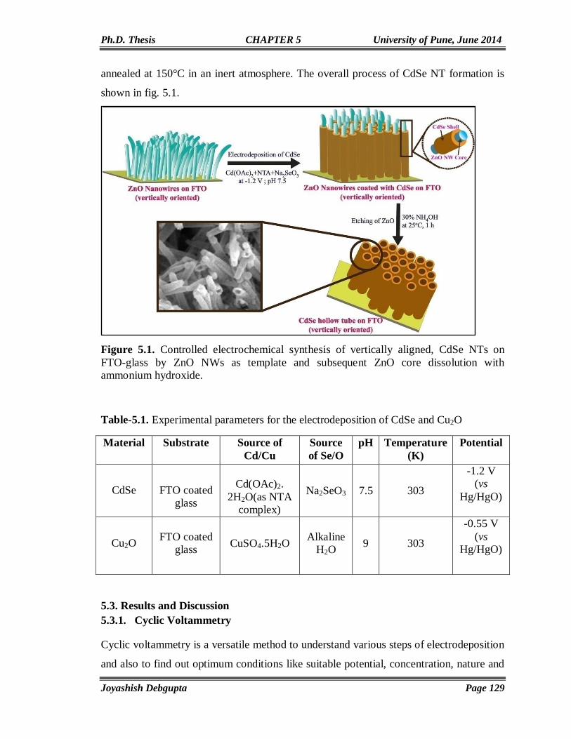
Ph.D. Thesis CHAPTER 5 University of Pune, June 2014
Joyashish Debgupta Page 129
annealed at 150°C in an inert atmosphere. The overall process of CdSe NT formation is
shown in fig. 5.1.
Figure 5.1. Controlled electrochemical synthesis of vertically aligned, CdSe NTs on FTO-glass by ZnO NWs as template and subsequent ZnO core dissolution with ammonium hydroxide.
Table-5.1. Experimental parameters for the electrodeposition of CdSe and Cu2O
Material Substrate Source of Cd/Cu
Source of Se/O
pH Temperature(K)
Potential
CdSe
FTO coated glass
Cd(OAc)2.
2H2O(as NTA complex)
Na2SeO3
7.5
303
-1.2 V (vs
Hg/HgO)
Cu2O
FTO coated
glass
CuSO4.5H2O
Alkaline
H2O
9
303
-0.55 V (vs
Hg/HgO)
5.3. Results and Discussion 5.3.1. Cyclic Voltammetry
Cyclic voltammetry is a versatile method to understand various steps of electrodeposition
and also to find out optimum conditions like suitable potential, concentration, nature and

Ph.D. Thesis CHAPTER 5 University of Pune, June 2014
Joyashish Debgupta Page 130
quantity of additives. Accordingly, cyclic voltammograms have been recorded in a
solution of 10 mM Cd(OAc)2, 5 mM Na2SeO3 and 50 mM NTA before electrodeposition.
Plausible reactions for CdSe formation can be summarized as follows,
𝑆𝑆𝑆𝑆𝑆𝑆32− + 3𝐻𝐻2𝑆𝑆 + 4𝑆𝑆− = 𝑆𝑆𝑆𝑆0 + 6𝑆𝑆𝐻𝐻−,𝐸𝐸0 = −0.36 𝑉𝑉𝑣𝑣𝑣𝑣 𝑁𝑁𝐻𝐻𝐸𝐸………………………………. (1)
𝑆𝑆𝑆𝑆0 + 2𝑆𝑆− = 𝑆𝑆𝑆𝑆2−,𝐸𝐸0 = −0.92 𝑉𝑉 𝑣𝑣𝑣𝑣 𝑁𝑁𝐻𝐻𝐸𝐸…………………………………………………… (2)
𝐶𝐶𝐶𝐶2+ + 𝑆𝑆𝑆𝑆2− = 𝐶𝐶𝐶𝐶𝑆𝑆𝑆𝑆 ↓………………………………………………………………………… (3)
Total cell reaction thus is,
𝑆𝑆𝑆𝑆𝑆𝑆32− + Cd2+ + 3𝐻𝐻2𝑆𝑆 + 6𝑆𝑆− = 𝐶𝐶𝐶𝐶𝑆𝑆𝑆𝑆 ↓ +6𝑆𝑆𝐻𝐻−
These reactions are similar to that reported previously for CdTe deposition.[19]But the
problem associated with the use of Na2SeO3 as a source of Se is that the standard redox
potential (ESeO 32−/Se 2−
o = -0.92 V)[20] for reducing SeO32- into Se2- is more than the
standard redox potential for Cd2+ (ECd 2+/Cdo = -0.40 V).[21] Hence, at the potential where
Se2- is generated, a significant amount of elemental Cd gets deposited along with the
formation of CdSe. This competing reaction, therefore, changes the composition of the
electrodeposited CdSe and results in poor quality of the resulting material. One way to
overcome this problem is to shift the formal reduction potential of Cd2+, by means of
complexation, [21] to such an extent that it cannot get reduced within the potential window
employed for the electro generation of Se2-. Nitrilotriacetic acid (NTA,
an aminopolycarboxylic acid ([N(CH2CO2H)3]) is employed for this purpose. NTA forms
a stable chelate (pK = 9.78) with Cd2+ion[22] and its formal potential is, therefore, shifted
significantly far negative so that Cd2+ does not get reduced prior to the reduction of
SeO32-. Eventually, the electrogenerated Se2- combines with the chelated Cd2+ to form
CdSe which then gets deposited on the substrate (FTO coated glass or ZnO NWs grown
on FTO coated glass). The above mechanism seems to be especially valid when we
consider all the features of the cyclic voltammograms (CVs) in fig. 5.2. Accordingly, fig.
5.2(a) shows a typical voltammogram in a solution of Cd(OAc)2 and NTA with FTO
coated glass as the working electrode. The voltammogram shows mostly capacitive
current and interestingly, no diffusion limited peak is clearly observed. The situation is,
however, different in the case of Na2SeO3 as evident from fig. 5.2(b). In contrast, this
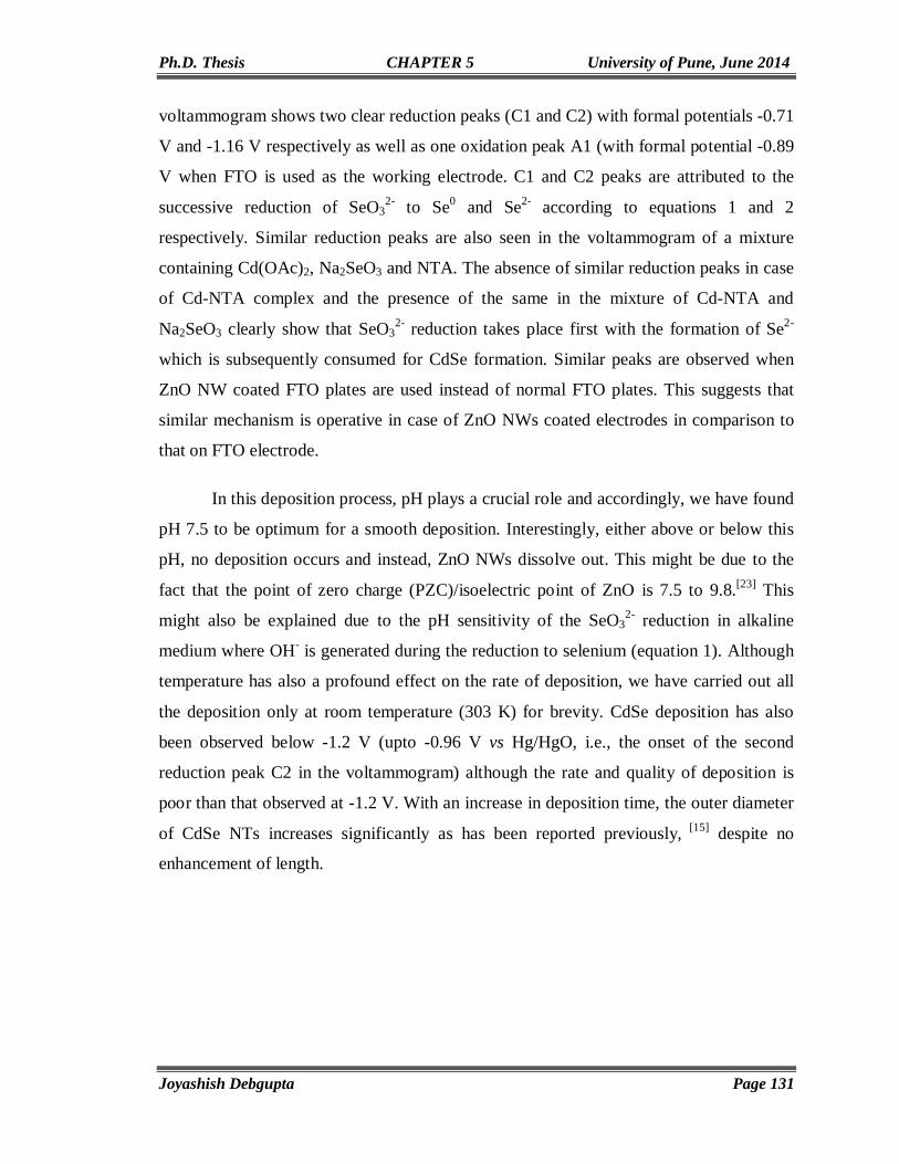
Ph.D. Thesis CHAPTER 5 University of Pune, June 2014
Joyashish Debgupta Page 131
voltammogram shows two clear reduction peaks (C1 and C2) with formal potentials -0.71
V and -1.16 V respectively as well as one oxidation peak A1 (with formal potential -0.89
V when FTO is used as the working electrode. C1 and C2 peaks are attributed to the
successive reduction of SeO32- to Se0 and Se2- according to equations 1 and 2
respectively. Similar reduction peaks are also seen in the voltammogram of a mixture
containing Cd(OAc)2, Na2SeO3 and NTA. The absence of similar reduction peaks in case
of Cd-NTA complex and the presence of the same in the mixture of Cd-NTA and
Na2SeO3 clearly show that SeO32- reduction takes place first with the formation of Se2-
which is subsequently consumed for CdSe formation. Similar peaks are observed when
ZnO NW coated FTO plates are used instead of normal FTO plates. This suggests that
similar mechanism is operative in case of ZnO NWs coated electrodes in comparison to
that on FTO electrode.
In this deposition process, pH plays a crucial role and accordingly, we have found
pH 7.5 to be optimum for a smooth deposition. Interestingly, either above or below this
pH, no deposition occurs and instead, ZnO NWs dissolve out. This might be due to the
fact that the point of zero charge (PZC)/isoelectric point of ZnO is 7.5 to 9.8.[23] This
might also be explained due to the pH sensitivity of the SeO32- reduction in alkaline
medium where OH- is generated during the reduction to selenium (equation 1). Although
temperature has also a profound effect on the rate of deposition, we have carried out all
the deposition only at room temperature (303 K) for brevity. CdSe deposition has also
been observed below -1.2 V (upto -0.96 V vs Hg/HgO, i.e., the onset of the second
reduction peak C2 in the voltammogram) although the rate and quality of deposition is
poor than that observed at -1.2 V. With an increase in deposition time, the outer diameter
of CdSe NTs increases significantly as has been reported previously, [15] despite no
enhancement of length.

Ph.D. Thesis CHAPTER 5 University of Pune, June 2014
Joyashish Debgupta Page 132
Figure 5.2. A comparison of Cyclic voltammograms of solutions containing (a) 10 mM Cd(OAc)2 and 50 mM Nitrilotriacetic acid (NTA), (b) only 5 mM Na2SeO3 with no NTA, (c) 10 mM Cd(OAc)2, 5 mM NTA and 50 mM Na2SeO3 and (d) same as (c) but using ZnO NWs grown FTO coated glass plate as working electrode; FTO coated glass plate is used as a working electrode in all cases from (a) to (c) except for (d) where ZnO NWs grown on FTO coated glass is the working electrode; Hg/HgO (0.1 M KOH) is used as reference and a platinum foil is used as counter electrode. Saturated NaOH is added to maintain the pH value of 7.5 in all cases and all measurements were done at 303 K.
5.3.2. Chronoamperometry
Chronoamperometry, i.e. study of current as a function of time at a constant potential, is
an important electrochemical technique, which gives valuable information about the
electrochemical process like electrodeposition, dissolution and other redox processes
occurring at the electrode surface. In the present study, this technique has been employed
to understand the mechanism of nucleation at the initial stage of deposition. Accordingly,
fig.5.3 shows representative chronoamperograms taken during the electrodeposition of
CdSe on plain FTO coated glass plate and also on ZnO NWs grown FTO coated glass
plates. Both the chronoamperograms show similar features, i.e., initial sharp increase in
current followed by a maximum current region at very short time scale (<50 s) and then
the maximum current decreases to a steady state at higher time scale (>50 s). However,

Ph.D. Thesis CHAPTER 5 University of Pune, June 2014
Joyashish Debgupta Page 133
the current density obtained in case of plain FTO coated glass plates is even with respect
to time (i.e., does not show ups and downs with time), whereas the current density for the
deposition on ZnO NWs shows small asperities as time progresses. These asperities may
originate due to roughness of ZnO NWs as compared to that on much less rough FTO
coated glass plates. This fact is reflected also in the total charge (Q, blue line) passed
during electrodeposition. Initial increase in current in the chronoamperograms is due to
nucleation, i.e., formation of nuclei on the substrate used on the application of potential
(the increment can be due to both the increase in total number of nuclei as well as the
growth of the initially formed nuclei). These nuclei then grow and ultimately coalesce
and form a continuous film on the substrate as has been predicted by the Volmer-Weber
growth model (because strong cohesive force between the nuclei surpasses the nuclei-
substrate adhesive interaction).[24] Coalescence of nuclei is reflected as a peak in the
chronoamperograms. After the maximum, the current density decreases to a steady state
value because of linear diffusion-limited growth and a planar film is formed, the
roughness of which does not change with time.[25,26] Thus Chronoamperometry is useful
in studying nucleation process during electrodeposition.
Figure 5.3. Chronoamperogram (pink line) during CdSe electrodeposition on (a) a plain FTO coated glass and (b) ZnO NW coated glass substrate; Blue line indicates total charge passed during electrodeposition; Chronoamperometry experiments were carried out with the same set-up used for cyclic voltammetry and the potential of the working electrode (FTO or ZnO NWs grown FTO coated glass plates) was held constant at -1.2 V vs Hg/HgO electrode for 15 min at (303 K).
According to the classical theory of nucleation, two fundamental categories of
nucleation processes can occur. [27] One of them is known as Instantaneous nucleation

Ph.D. Thesis CHAPTER 5 University of Pune, June 2014
Joyashish Debgupta Page 134
where all the nuclei are formed at the same time upon the application of potential
followed by their collective subsequent growth.[27] The other category is the progressive
nucleation in which nuclei are formed one after another, (i.e., progressive formation of
nuclei). Scharifker and Hills proposed a quantitative treatment for this three-dimensional
multiple nucleation with diffusion controlled growth. [28] According to their treatment, the
nuclei are thought of hemispherical in shape and those nuclei grow in size due to
spherical diffusion at short time scale, but at higher time the diffusion field of individual
nucleus merge together and finally growth occurs due to linear diffusion. Fig. 5.4 shows
schematically the diffusion field around each nucleus.
Figure 5.4. Schematic representation of the diffusion zones of individual nuclei and their eventual merging at higher time scale. [28]
They proposed two equations to describe the current transients obtained for the two
different modes of nucleation as follows:
( 𝑖𝑖𝑖𝑖𝑚𝑚
)2 = 1.9542𝑡𝑡𝑡𝑡𝑚𝑚
1− exp[−1.2564 𝑡𝑡𝑡𝑡𝑚𝑚]2...................................................................(3)
(𝑖𝑖𝑖𝑖𝑚𝑚
)2 =1.2254
𝑡𝑡𝑡𝑡𝑚𝑚
1− exp −2.3367(𝑡𝑡𝑡𝑡𝑚𝑚
)22
… … … … … … … … … … … … … … … … . . (4)
where, i is the observed current, im, the maximum current in the current-time transient
(chronoamperogram), and tm corresponds to the time for the maximum current.

Ph.D. Thesis CHAPTER 5 University of Pune, June 2014
Joyashish Debgupta Page 135
Equation 3 describes the case of instantaneous nucleation whereas; equation 4 is for
progressive nucleation. These two equations are often regarded as diagnostic criteria for
the two different types of nucleation. A general observation for potentiostatic current-
time transient during electrodeposition is that the current maximum shifts towards lower
time as the applied potential becomes more and more negative. This also happens in the
present case as has been observed in fig. 5.5(a).
In order to understand the type of nucleation mechanism during the electrodeposition of
CdSe on ZnO NWs grown on FTO coated glass plate, the current-time transients
(chronoamperogram) can be further subdivided into three distinct regions (fig. 5.5(b)):
Region-I: Very short time region where the current is inversely proportional to the square
root of time [fig. 5.5(d)]and thus indicates that the process is under diffusion controlled.
Such a dependency is in accordance with the Cottrell behaviour and is indicative of
instantaneous nucleation where all the nuclei form at the same time. [28]
Region-II: Intermediate time region where the current reaches its maximum value and
then decays according to the Cottrell relation. So formed nuclei in region-I, start to
coalesce near to the peak maximum and at the peak maximum all the nuclei merge
together to form a continuous film.
Region-III: This is the region where there is continuous film growth governed by the
linear diffusion.
To further confirm the mode of nucleation, dimensionless current-time plot (i2/im2 vs t/tm)
has been constructed according to the equations 3 and 4. Fig. 5.5(c) is a comparison of
the dimensionless current-time plots obtained from the experimental data to the plots
obtained from equation 3 and 4. In the present case the normalized current-time
relationship follows the behaviour known for instantaneous nucleation mechanism. It is
clearly observed that in the short-time region the kinetics of nucleation follows the
instantaneous pathway rather than the progressive one although it deviates when t is
increasingly greater than tm.

Ph.D. Thesis CHAPTER 5 University of Pune, June 2014
Joyashish Debgupta Page 136
Figure 5.4. (a) Current density-time transients (chronoamperograms) at various potentials for the electrodeposition of CdSe on ZnO NWs grown FTO coated glass plates; Maximum current occurs at lesser time as the potential becomes more negative; (b) Current density-time profile for electrodeposition at -1.2 V vs Hg/HgO; Nucleation and growth zones are highlighted with different colors; (c) Dimensionless (j/jm)2vs t/tm plot for the data in (b); Red dots are the experimental points and solid lines are obtained from eqn.3 and 4; (d) Current density vs t-1/2 plot obtained from very short time regime (4-5 s); Linear behavior of j with the inverse of square root of t proves the Cottrell type diffusion and thereby proves instantaneous nucleation.
5.3.3. Scanning Electron Microscopy (SEM) and EDAX
Scanning electron micrographs of ZnO NWs as well as CdSe NTs on FTO coated
glass plates are shown in fig. 5.5(a) and 5.5(b) respectively. All ZnO NWs are ~2.5 µm
long having ~170-200 nm diameter and reveal nearly vertical alignment with respect to
the substrate (FTO coated glass) plane and the approximate density of the as-grown
nanowires is ~3 x 109 cm-2. However, after CdSe deposition, the diameter of each NW
increases and more significantly, the surface becomes rough (fig. 5.5(c) and 5.5(d))
indicating the successful deposition on the walls of ZnO NWs. In comparison, after
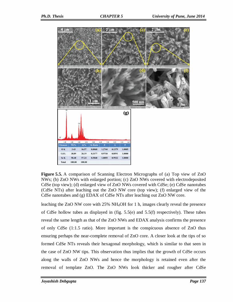
Ph.D. Thesis CHAPTER 5 University of Pune, June 2014
Joyashish Debgupta Page 137
Figure 5.5. A comparison of Scanning Electron Micrographs of (a) Top view of ZnO NWs; (b) ZnO NWs with enlarged portion; (c) ZnO NWs covered with electrodeposited CdSe (top view); (d) enlarged view of ZnO NWs covered with CdSe; (e) CdSe nanotubes (CdSe NTs) after leaching out the ZnO NW core (top view); (f) enlarged view of the CdSe nanotubes and (g) EDAX of CdSe NTs after leaching out ZnO NW core.
leaching the ZnO NW core with 25% NH4OH for 1 h, images clearly reveal the presence
of CdSe hollow tubes as displayed in (fig. 5.5(e) and 5.5(f) respectively). These tubes
reveal the same length as that of the ZnO NWs and EDAX analysis confirms the presence
of only CdSe (1:1.5 ratio). More important is the conspicuous absence of ZnO thus
ensuring perhaps the near-complete removal of ZnO core. A closer look at the tips of so
formed CdSe NTs reveals their hexagonal morphology, which is similar to that seen in
the case of ZnO NW tips. This observation thus implies that the growth of CdSe occurs
along the walls of ZnO NWs and hence the morphology is retained even after the
removal of template ZnO. The ZnO NWs look thicker and rougher after CdSe

Ph.D. Thesis CHAPTER 5 University of Pune, June 2014
Joyashish Debgupta Page 138
electrodeposition (fig. 4(d)) than that of the pristine NWs. Tip of CdSe NTs retains the
hexagonal shape (170-200 nm diameter and 2.5 µm in length) of ZnO NW tip and
thereby gives further evidence for nanowire templating. In order to further confirm the
role of ZnO NWs as template, we have carried out deposition on plain FTO without
having any ZnO NWs grown on it. Accordingly, fig. 5.6(c) and (d) show images of the
electrodeposited CdSe on plain FTO coated glass substrate. It does not show any specific
morphology and the thin film (~300 nm thick) consists of only particles of CdSe. Fig.
5.6(a) shows vertical cross section of CdSe nanotubes supported on FTO base coated on
glass plate and fig. 5.6(b) is the enlarged view for the same. This clearly demonstrates the
importance of ZnO NWs as template. Fig. 5.6(d) is the representative SEM image of
electrodeposited Cu2O on FTO coated glass. The film appears to be uniform throughout
the FTO coated glass surface with no characteristic morphology.
Figure 5.6. Scanning Electron micrographs of (a) CdSe NTs on FTO coated glass substrates showing vertical cross section where CdSe nanotubes are seen standing vertically on FTO coated glass; (b) enlarged view of the vertical cross section; (c) Thin film of electrodeposited CdSe on plain FTO coated glass without ZnO NW coating (top view) and (d) top view of electrodeposited Cu2O film on FTO coated glass plate; Uniform coating is observed throughout the substrate.
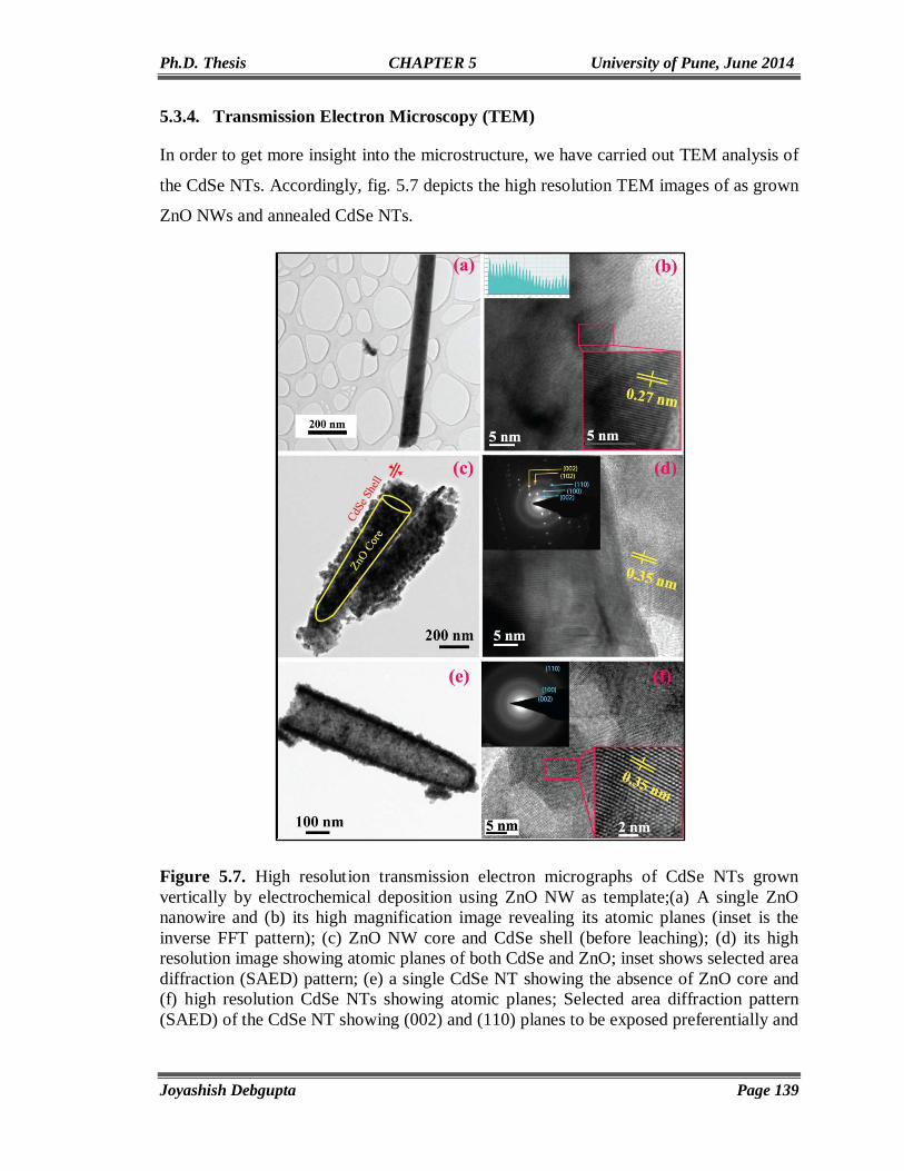
Ph.D. Thesis CHAPTER 5 University of Pune, June 2014
Joyashish Debgupta Page 139
5.3.4. Transmission Electron Microscopy (TEM)
In order to get more insight into the microstructure, we have carried out TEM analysis of
the CdSe NTs. Accordingly, fig. 5.7 depicts the high resolution TEM images of as grown
ZnO NWs and annealed CdSe NTs.
Figure 5.7. High resolution transmission electron micrographs of CdSe NTs grown vertically by electrochemical deposition using ZnO NW as template;(a) A single ZnO nanowire and (b) its high magnification image revealing its atomic planes (inset is the inverse FFT pattern); (c) ZnO NW core and CdSe shell (before leaching); (d) its high resolution image showing atomic planes of both CdSe and ZnO; inset shows selected area diffraction (SAED) pattern; (e) a single CdSe NT showing the absence of ZnO core and (f) high resolution CdSe NTs showing atomic planes; Selected area diffraction pattern (SAED) of the CdSe NT showing (002) and (110) planes to be exposed preferentially and
Ph.D. Thesis CHAPTER 5 University of Pune, June 2014
Joyashish Debgupta Page 140
lattice planes with a d-spacing of 0.35 Å indicating primitive hexagonal crystal structure of the nanotubes.
The diameter of a single ZnO NWs is ~60-70 nm (fig. 5.7(a)), but the diameter is
found to increase (~242 nm) after electrodeposition of CdSe on ZnO NWs as is clear
from fig. 5.7(c). On the other hand, the diameter of CdSe shell does not change after the
dissolution of ZnO NW core (fig. 5.7(e)). Moreover, a comparative study of high
resolution images of ZnO NW, CdSe deposited ZnO NWs and CdSe NTs (fig. 5.7(b),
5.7(d) and (f) respectively) reveals the presence of CdSe shell on ZnO core, mainly
because the lattice fringe patterns are different in three different cases. Indexing of the
diffraction spots for ZnO reveals (002) and (102) planes are mostly exposed. For
example, in fig. 5.7(b), the outer wall of the nanowires shows a characteristic d-spacing
of 2.7 Å for ZnO, whereas fig. 5.7(d) shows two different types of d-spacing values-the
outer portion (edge) mainly comprises of CdSe (3.5 Å) while the centre region has two
types of lattice fringes due to the presence of both CdSe and ZnO. Thus TEM analysis
proves the critical role of ZnO NWs as template for the growth of hollow CdSe NTs. As
can be seen from fig. 5.7(e) and 5.7(f), the surface of each CdSe NT is granular and
consists of CdSe nanoparticles of size 8-10 nm (fig. 5.7(f)) as illustrated in the enlarged
view of fig. 5.7(e). These nanoparticles are deposited on the walls of ZnO NWs and
linked together to form a tubular morphology. These particles are interconnected by
strong cohesive forces as they do not get separated easily even upon ultrasonication,
which is especially relevant for the sample after annealing at 300°C in N2 atmosphere.
Fig. 5.7(f) is a representative selected area electron diffraction pattern (SAED) of the
CdSe NTs.
The sharp nature of the diffraction rings is indicative of polycrystalline nature of
the CdSe NTs and an assignment of the rings shows that (002) plane is more intense than
the (110) plane. This, thus implies that the growth of CdSe NTs is mainly along the
<002> direction (c-axis). The d-spacing values obtained both from SAED as well as
lattice fringes (3.5 Å) is in good confirmation with the primitive hexagonal phase
formation (JCPDS card no. 77-0046) and matches well with that obtained previously.[29]
The core-shell nature of ZnO NW-CdSe is also evident from the SAED. Its high
magnification image (fig. 5(d)), revealing its atomic planes, shows ZnO NW core and

Ph.D. Thesis CHAPTER 5 University of Pune, June 2014
Joyashish Debgupta Page 141
CdSe shell (before leaching) and the inset shows selected area electron diffraction
(SAED) pattern for the same. Fig. 5.7(e) is the representative TEM image of a single
CdSe NTs showing the absence of ZnO core while fig. 5.7(f) is the high resolution image
of CdSe NTs showing atomic planes. SAED of the CdSe NT shows (002) and (110)
planes to be exposed preferentially. Lattice plane with a d-spacing of 3.5 Å, indicates
primitive hexagonal crystal structure of the nanotubes. SAED patterns of ZnO NWs and
CdSe/ZnO NWs hybrids as well as CdSe NTs are shown in the inset of fig. 5.7(b), 5.7(d)
and 5.7(f) respectively. For ZnO/CdSe system (before leaching the ZnO), two different
types of SAED spots are observed (fig. 5.7(d)), whereas in case of CdSe NTs (fig. 5.7(f)),
only ring pattern is observed. This is because of the presence of both ZnO and CdSe
particles after electrodeposition, again confirming the core-shell nature of the hybrids.
However, after leaching out the core ZnO, the characteristic dot SAED pattern disappears
and only ring patterns of CdSe is observed. This is also an indication of complete
removal of ZnO.
5.3.5. Micro Raman
Fig. 5.8 shows the micro Raman spectrum of CdSe NTs, recorded using a 632.8 nm laser
line with a 50x objective lens. For comparison, the Raman spectrum of electrodeposited
CdSe nanoparticles (CdSe NPs on FTO coated glass without any ZnO NW template) is
also displayed along with that of CdSe NTs. Both the spectra show characteristic
longitudinal optical phonon (LO) modes arising due to Se-Cd-Se symmetric vibration [30]
at 205 cm-1 for CdSe NPs and at 208 cm-1 for CdSe NTs. The appearance of a peak below
210 cm-1 confirms that CdSe is in the nanosize range because the same peak comes at 210
cm-1 for bulk CdSe.
The second order bands (2LO) also appear in the spectra at 408 cm-1 for CdSe NPs and
at 415 cm-1 in case of CdSe NTs. This band originates due to a double resonance process
during the Raman scattering. Interestingly, both positions of LO and 2LO peaks of CdSe
NT are shifted to a higher wave number (or higher energy) by 3 and 7 cm-1 respectively
than that of CdSe NPs. Interestingly, FWHM of LO peak also decreases slightly in the
case of CdSe NTs than that of CdSe NPs. This ostensibly suggests quantum confinement
effect, since both the LO and 2LO peak frequencies show a blue shift. However, a careful

Ph.D. Thesis CHAPTER 5 University of Pune, June 2014
Joyashish Debgupta Page 142
inspection of the TEM images suggests that the nanoparticles consisting the NTs, are of
8-10 nm in size which is far beyond the strong confinement region for CdSe (exciton
Bohr radius is 5.4 nm for bulk CdSe).[31] Hence quantum confinement is not expected to
explicitly contribute to the shift of the phonon peaks. A more appropriate explanation for
the shift might be the presence of surface traps. It is well known that CdSe nanoparticles
(NPs) have surface defects (or traps) due to more surface-to-volume ratio and the extent
of defect increases when the nanoparticles assemble into a quasi 1D structure like
nanotubes.[32] So the net surface defect content is significantly higher in case of CdSe
NTs than that for CdSe NPs. This higher defect content may be responsible for shifting
the fundamental phonon modes of CdSe NPs to higher energy. [32] Interestingly, no peak
is observed for selenium (Se) and this cancels out the possibility of the presence of excess
Se on the surface of CdSe during electrodeposition.
Figure 5.8. A comparison of the Micro Raman spectra of CdSe nanoparticles (black line) with that of CdSe nanotubes (red line); All the measurements were taken using 632.8 nm He-Ne laser line (20 mW source energy) with 50x objective lens; No density filter was used for the measurement; Insets are the enlarged portion of the LO (200-214 cm-1) and 2LO (360-450 cm-1) bands respectively; Both the bands shift bathochromically in case of nanotubes, although the amount of shift is more for 2LO band.
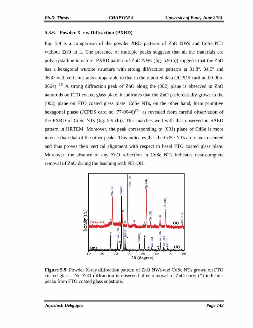
Ph.D. Thesis CHAPTER 5 University of Pune, June 2014
Joyashish Debgupta Page 143
5.3.6. Powder X-ray Diffraction (PXRD)
Fig. 5.9 is a comparison of the powder XRD patterns of ZnO NWs and CdSe NTs
without ZnO in it. The presence of multiple peaks suggests that all the materials are
polycrystalline in nature. PXRD pattern of ZnO NWs (fig. 5.9 (a)) suggests that the ZnO
has a hexagonal wurzite structure with strong diffraction patterns at 31.8°, 34.5° and
36.4° with cell constants comparable to that in the reported data (JCPDS card no.00-005-
0664).[33] A strong diffraction peak of ZnO along the (002) plane is observed in ZnO
nanorods on FTO coated glass plate; it indicates that the ZnO preferentially grows in the
(002) plane on FTO coated glass plate. CdSe NTs, on the other hand, form primitive
hexagonal phase (JCPDS card no. 77-0046)[29] as revealed from careful observation of
the PXRD of CdSe NTs (fig. 5.9 (b)). This matches well with that observed in SAED
pattern in HRTEM. Moreover, the peak corresponding to (001) plane of CdSe is more
intense than that of the other peaks. This indicates that the CdSe NTs are c-axis oriented
and thus proves their vertical alignment with respect to basal FTO coated glass plate.
Moreover, the absence of any ZnO reflection in CdSe NTs indicates near-complete
removal of ZnO dur ing the leaching with NH4OH.
Figure 5.9. Powder X-ray diffraction pattern of ZnO NWs and CdSe NTs grown on FTO coated glass ; No ZnO diffraction is observed after removal of ZnO core; (*) indicates peaks from FTO coated glass substrate.
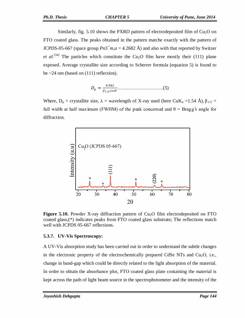
Ph.D. Thesis CHAPTER 5 University of Pune, June 2014
Joyashish Debgupta Page 144
Similarly, fig. 5.10 shows the PXRD pattern of electrodeposited film of Cu2O on
FTO coated glass. The peaks obtained in the pattern matche exactly with the pattern of
JCPDS-05-667 (space group Pn3¯m,a = 4.2682 Å) and also with that reported by Switzer
et al.[34] The particles which constitute the Cu2O film have mostly their (111) plane
exposed. Average crystallite size according to Scherrer formula (equation 5) is found to
be ~24 nm (based on (111) reflection).
𝐷𝐷𝑝𝑝 = 0.94𝜆𝜆𝛽𝛽1/2𝑐𝑐𝑐𝑐𝑣𝑣𝑐𝑐
………………………..(5)
Where, Dp = crystallite size, λ = wavelength of X-ray used (here CuKα =1.54 Å), β 1/2 =
full width at half maximum (FWHM) of the peak concerned and θ = Bragg’s angle for
diffraction.
Figure 5.10. Powder X-ray diffraction pattern of Cu2O film electrodeposited on FTO coated glass;(*) indicates peaks from FTO coated glass substrate; The reflections match well with JCPDS 05-667 reflections. 5.3.7. UV-Vis Spectroscopy:
A UV-Vis absorption study has been carried out in order to understand the subtle changes
in the electronic property of the electrochemically prepared CdSe NTs and Cu2O, i.e.,
change in band-gap which could be directly related to the light absorption of the material.
In order to obtain the absorbance plot, FTO coated glass plate containing the material is
kept across the path of light beam source in the spectrophotometer and the intensity of the

Ph.D. Thesis CHAPTER 5 University of Pune, June 2014
Joyashish Debgupta Page 145
transmitted light is measured. Accordingly, fig. 5.11 (a) shows a comparison of the
absorption spectrum of CdSe NTs, where a broad hump of maximum absorption is
observed at 650 nm followed by a small shoulder at 550 nm. The hump is related to the
first excitonic transition (1s-1p) in CdSe [35] and the shoulder is due to the second exciton
generation. After this the spectrum gradually shoots up as the wavelength decreases or
energy increases. The onset of absorption is 750 nm which corresponds to a bandgap
energy of 1.8 eV which is close to the bulk bandgap value of CdSe.[36] The higher
bandgap value can be justified by considering that the CdSe NTs are composed of CdSe
nanocrystallites while lower value enables it to absorb strongly in the visible region.
Figure 5.11. A comparison of the UV-Vis absorbance spectra of electrodeposited (a) CdSe NTs and (b) Cu2O on FTO coated glass; CdSe NTs show one broad peak followed by a small hump, Cu2O shows one peak and two broad humps;Inset of (b) shows the corresponding Tauc plot showing the direct band gap transition for the material (Cu2O);(c) UV-Vis absorption spectra of ZnO NWs-CdSe at different time of leaching ZnO NWs with 25% NH4OH solution; plateau within the range 550-350 nm corresponds to ZnO absorption and is found to decrease with increase in leaching time; This indicates a gradual removal of ZnO along with the formation of CdSe nanotubes.
A similar UV-Vis absorption study has also been carried out to find out the proper
time required to leach out completely the ZnO NW core using NH4OH. A FTO coated
Ph.D. Thesis CHAPTER 5 University of Pune, June 2014
Joyashish Debgupta Page 146
glass plate containing CdSe coated ZnO NWs has been dipped in 25% NH4OH solution
for etching. The plate has been taken out periodically after every 15 m, washed and
absorbance has been measured. Fig. 5.11 (c) shows the absorbance plot at different
etching duration. It is found that the ZnO absorption feature completely vanishes after 1
h. On the other hand, the absorption spectrum clearly shows one broad hump at 650 nm,
corresponding to CuO formed during the exposure of the Cu2O sample in the atmosphere,
and two peaks with λmax 452 nm and 340 nm. The peak at 452 nm corresponds to the
band edge transition for p-type Cu2O and the other peak at 340 nm is due to band-to-band
transition in Cu2O.[37] The band gap of Cu2O turns out to be 2.4 eV as calculated from
the Tauc plot. However, bulk Cu2O has a band gap of 2.2 eV. The observation of slightly
higher band gap in this case can be attributed to the fact that the electrodeposited film
consists of Cu2Onanoparticles having average crystallite size ~24 nm (as obtained from
PXRD) so that perhaps a negligible contribution comes from the higher band gap energy
(i.e., quantum confinement effect).[37]
5.3.8. Photoluminescence
Fig. 5.12 shows a comparison of the steady state photoluminescence (emission) spectra of
CdSe NTs (a) and electrodeposited film of Cu2O (b) collected by exciting the samples at
their band edge energy. The photoluminescence (PL) spectrum of CdSe nanotubes is
broad and centered at 662 nm when excited at 650 nm which is the transition energy for
CdSe (1Sh-1Se transition). The Stoke’s shift in this case is ~12 nm (103.3 eV) which
matches well with similar values. [38] More specifically, Cu2O shows three emissions
when excited with 450 nm to 531.7 nm (band edge emission), 528 nm and another at
687.6 nm.

Ph.D. Thesis CHAPTER 5 University of Pune, June 2014
Joyashish Debgupta Page 147
Figure 5.12. Photoluminescence spectra of (a) CdSe NTs and (b) electrodeposited Cu2O; CdSe NT shows one broad peak centered around 662 nm (excitation wavelength is 650 nm); Cu2O shows three emission peaks (531.7 nm, 528 nm and 687.6 nm) when excited with 450 nm wavelength light.
5.3.9. Mott-Schottky Plot
Capacitance measurement on the electrode/electrolyte interface has been carried out to
determine the flat band (Efb) potential of the material and carrier density (NA), which are
important parameters to describe a semiconductor electrode/electrolyte interface. When a
semiconductor comes in contact with an electrolyte solution, semiconductor Fermi level
tends to align itself with the Fermi level of the electrolyte solution, until equilibrium is
established. As a result, the valence and conduction bands shift upward or downward
(depending on the position of the two Fermi levels before contact). Efb is a measure of the
Figure 5.13. Mott-Schottky plot for (a) n-type CdSe NTs and (b) p-type Cu2O; Impedance is carried out in Na2S-Na2SO3 solution for CdSe NTs and in 0.1 M NaOAc

Ph.D. Thesis CHAPTER 5 University of Pune, June 2014
Joyashish Debgupta Page 148
aq. solution for Cu2O; nature of the plots suggests that CdSe NT is n-type semiconductor while the electrodeposited Cu2O is a p-type semiconductor.
extent of band bending, when a semiconductor electrode is brought in contact with an
electrolyte solution. More importantly, both Efb and carrier density (NA) can be
determined from the Mott-Schottky plot, which is a plot of 1/C2 vs applied potential at a
fixed frequency (where, C is the space charge capacitance of the semiconductor) of 20
kHz. The capacitance measurements are presented as per the equation (Mott-Schottky
equation):[21] 1𝐶𝐶2 = 2
𝑁𝑁𝐴𝐴𝜀𝜀𝜀𝜀0𝑆𝑆[𝐸𝐸 − 𝐸𝐸𝑓𝑓𝑓𝑓 −
𝑘𝑘𝑘𝑘𝑆𝑆]…………… (6)
where, C is the interfacial capacitance (i.e., capacitance of the semiconductor depletion
layer), ε is the dielectric constant of the material, ε0 is the permittivity of free space (8.85
x 10-12 Fm-1), NA is the number density (cm-3) of donors/acceptors in the semiconductor
(doping level), E is the applied potential, Efb is the flat band potential, T is the absolute
temperature (298 K), k is the Boltzmann constant (1.38 x 10⁻²³ JK-1) and e is the electron
charge (1.6 x 10⁻¹⁹ C). The temperature term is generally small and can be neglected.
Fig. 5.13 accordingly shows Mott-Schottky (MS) plot for both CdSe NTs and Cu2O. The
nature of the plots suggests that CdSe is n-type while Cu2O is a p-type semiconductor.
Moreover, the intercept of the plot on potential (E) axis (at y = 0) is the Efb of the material
for a specific electrode /electrolyte interface. Hence, the Efb of CdSe NTs is -0.76 V vs
Hg/HgO and that for Cu2O is 0.92 V vs Hg/HgO at room temperature (303 K). Carrier
density (NA) as calculated from the slope of the MS plot is found to be 7.3 x 10¹⁶ m-3for
CdSe NTs (electron is the majority carrier) and 1.09 x 10¹⁷ m-3for Cu2O (hole is the
majority carrier). These values obtained are quite similar with that reported for CdSe[39]
and Cu2O[40].
5.3.10. Properties of CdSe NTs-Cu2O flip-chip n-p Heterojunction Diode
Cu2O is a well-known p-type material (since the majority carrier is hole and not electron
due to its natural propensity to form cation vacancies) with a band gap of 2.2 eV [41] and
its valence and conduction bands (VB and CB respectively) are at 1.30 and -0.70 V (vs
NHE) respectively. These bands are well aligned with the VB and CB of CdSe (1.32 and
-0.59 V vs NHE). [42] Hence, a remarkable combination of both these two can in principle
Ph.D. Thesis CHAPTER 5 University of Pune, June 2014
Joyashish Debgupta Page 149
give rise to important heterojunction (fig. 5.14 (a)), which can show good optoelectronic
properties. FTO coated glass plate containing CdSe NTs can be brought into intimate
contact with the FTO coated glass plate containing Cu2O in order to establish the n-p
hetero-junction. Here, the CdSe has a band-gap of 1.8 eV while that of Cu2O is 2.4 eV.
The device shows rectifying behaviour under dark with a rectification ratio (Iforward/Ireverse)
of 3 at a bias of 0.6 V, indicating the formation of a p-n junction diode. The “turn on”
voltage is 0.13 V and the reverse leakage current value is 7 x 10⁻⁵ A at -1 V (Fig. 5.14
(b)).[43] In order to see the effect of CdSe NT/FTO and Cu2O/FTO junctions on the I-V
characteristic of the n-p heterojunction, I-V measurement has been carried out for the
respective junctions in a similar flip-chip method. Accordingly, fig. 5.14 (c) and (d) show
I-V characteristics of CdSe NT/FTO and Cu2O/FTO junctions respectively. Cu2O/FTO
junction shows ohmic behavior at very low voltage (within ± 0.04 V), but changes to
Schottky type at voltage larger than this threshold voltage. On the other hand, CdSe
NT/FTO junction shows ohmic behavior upto ~0.6 V.Although absorption spectrum of
electrodeposited Cu2O (fig. 5.11 (b)) shows the presence of very small amount of CuO
formed due to aerial oxidation on the surface of Cu2O, but the presence of CuO (a p-type
Mott insulator) does not affect the electron transfer from p-type Cu2O because the
valence and conduction bands of the latter are properly aligned with CdSe (fig. 5.14 (a))
so as to allow electron transfer from p-type Cu2O to n-type CdSe NTs upon external
excitation. Due to the difference in Fermi energy of the n and p-type materials as well as
due to the different nature of majority carriers, an intrinsic potential builds up at the
interface between the two. This potential assists in separating the photo generated carriers
at the interface.
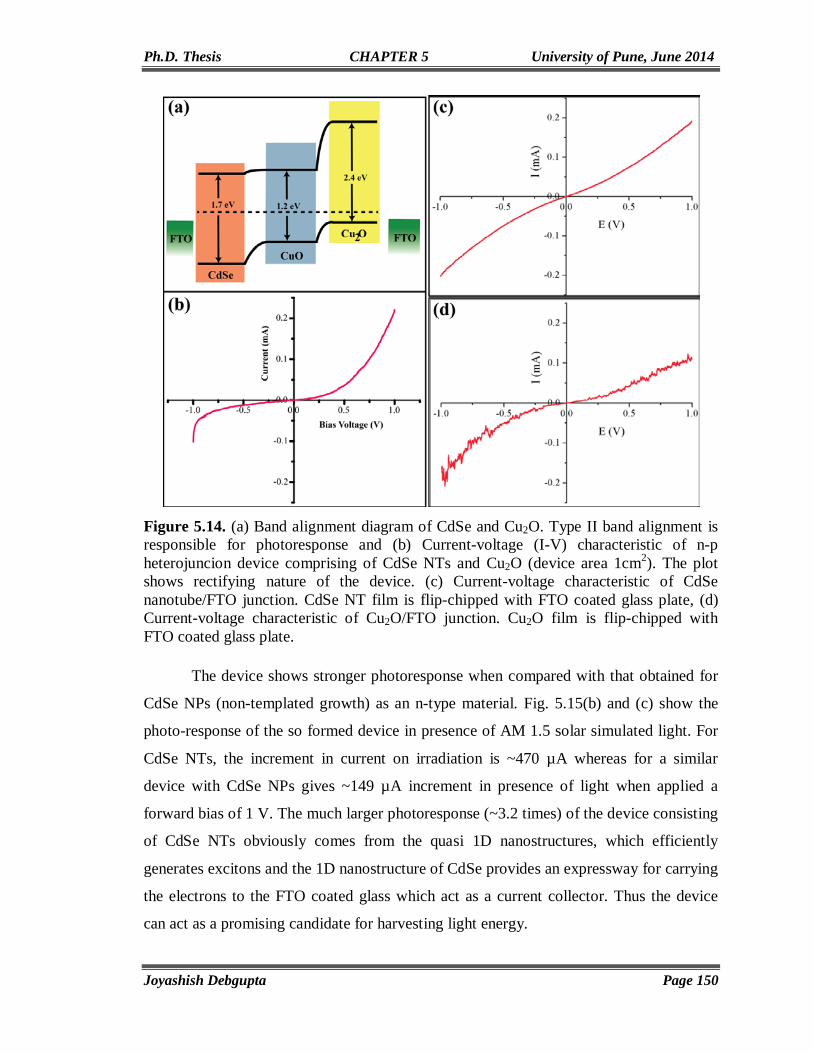
Ph.D. Thesis CHAPTER 5 University of Pune, June 2014
Joyashish Debgupta Page 150
Figure 5.14. (a) Band alignment diagram of CdSe and Cu2O. Type II band alignment is responsible for photoresponse and (b) Current-voltage (I-V) characteristic of n-p heterojuncion device comprising of CdSe NTs and Cu2O (device area 1cm2). The plot shows rectifying nature of the device. (c) Current-voltage characteristic of CdSe nanotube/FTO junction. CdSe NT film is flip-chipped with FTO coated glass plate, (d) Current-voltage characteristic of Cu2O/FTO junction. Cu2O film is flip-chipped with FTO coated glass plate.
The device shows stronger photoresponse when compared with that obtained for
CdSe NPs (non-templated growth) as an n-type material. Fig. 5.15(b) and (c) show the
photo-response of the so formed device in presence of AM 1.5 solar simulated light. For
CdSe NTs, the increment in current on irradiation is ~470 µA whereas for a similar
device with CdSe NPs gives ~149 µA increment in presence of light when applied a
forward bias of 1 V. The much larger photoresponse (~3.2 times) of the device consisting
of CdSe NTs obviously comes from the quasi 1D nanostructures, which efficiently
generates excitons and the 1D nanostructure of CdSe provides an expressway for carrying
the electrons to the FTO coated glass which act as a current collector. Thus the device
can act as a promising candidate for harvesting light energy.

Ph.D. Thesis CHAPTER 5 University of Pune, June 2014
Joyashish Debgupta Page 151
Figure 5.15. (a) A schematic representation of the flip-chip n-p heterojunction device fabricated. Current is measured perpendicular to the plane of the FTO plate. Current-voltage (I-V) characteristics of CdSe–Cu2O heterojunction devices (n-p junction) in dark (black) and under AM 1.5 solar simulated light (i.e., 100 mWcm-2) (red), (b) corresponds to the device with CdSe Nanoparticles (NPs)-Cu2O and (c) with CdSe NTs-Cu2O, (d) Nyquist plot for the device under dark and light; The first semicircle remains unchanged while the second one decreases upon illumination with AM 1.5 solar simulated light.
Fig. 5.15 (d) represents the Nyquist plot for the device under dark and illuminated
conditions. Interestingly, the low frequency semicircle decreases (319 Ω) upon
illumination indicating probably the reduced charge transfer resistance at the interface.
The valence band (VB) and conduction band (CB) of CdSe are well aligned with that of
Cu2O and hence the photo-generated minority carriers (electron) in Cu2O can be easily
transferred to the CB of CdSe NTs. At the same time the hole can migrate from the VB of
CdSe to the Cu2O VB (fig.5.14 (a)). This thereby reduces the probability of
recombination leading to a decrease in charge transfer resistance as well as an improved
photocurrent generation in the case of CdSe NTs and Cu2O hetero-junction.
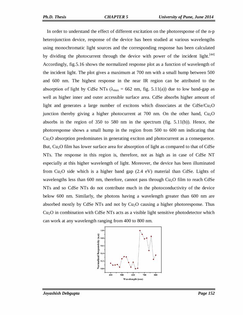
Ph.D. Thesis CHAPTER 5 University of Pune, June 2014
Joyashish Debgupta Page 152
In order to understand the effect of different excitation on the photoresponse of the n-p
heterojunction device, response of the device has been studied at various wavelengths
using monochromatic light sources and the corresponding response has been calculated
by dividing the photocurrent through the device with power of the incident light.[44]
Accordingly, fig.5.16 shows the normalized response plot as a function of wavelength of
the incident light. The plot gives a maximum at 700 nm with a small hump between 500
and 600 nm. The highest response in the near IR region can be attributed to the
absorption of light by CdSe NTs (λmax = 662 nm, fig. 5.11(a)) due to low band-gap as
well as higher inner and outer accessible surface area. CdSe absorbs higher amount of
light and generates a large number of excitons which dissociates at the CdSe/Cu2O
junction thereby giving a higher photocurrent at 700 nm. On the other hand, Cu2O
absorbs in the region of 350 to 580 nm in the spectrum (fig. 5.11(b)). Hence, the
photoresponse shows a small hump in the region from 500 to 600 nm indicating that
Cu2O absorption predominates in generating exciton and photocurrent as a consequence.
But, Cu2O film has lower surface area for absorption of light as compared to that of CdSe
NTs. The response in this region is, therefore, not as high as in case of CdSe NT
especially at this higher wavelength of light. Moreover, the device has been illuminated
from Cu2O side which is a higher band gap (2.4 eV) material than CdSe. Lights of
wavelengths less than 600 nm, therefore, cannot pass through Cu2O film to reach CdSe
NTs and so CdSe NTs do not contribute much in the photoconductivity of the device
below 600 nm. Similarly, the photons having a wavelength greater than 600 nm are
absorbed mostly by CdSe NTs and not by Cu2O causing a higher photoresponse. Thus
Cu2O in combination with CdSe NTs acts as a visible light sensitive photodetector which
can work at any wavelength ranging from 400 to 800 nm.
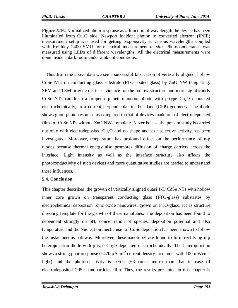
Ph.D. Thesis CHAPTER 5 University of Pune, June 2014
Joyashish Debgupta Page 153
Figure 5.16. Normalized photo-response as a function of wavelength the device has been illuminated from Cu2O side. Newport incident photon to converted electron (IPCE) measurement setup was used for getting responsivity at various wavelengths coupled with Keithley 2400 SMU for electrical measurement in situ. Photoconductance was measured using LEDs of different wavelengths. All the electrical measurements were done inside a dark room under ambient conditions.
Thus from the above data we see a successful fabrication of vertically aligned, hollow
CdSe NTs on conducting glass substrate (FTO coated glass) by ZnO NW templating.
SEM and TEM provide distinct evidence for the hollow structure and more significantly
CdSe NTs can form a proper n-p heterojunction diode with p-type Cu2O deposited
electrochemically, in a current perpendicular to the plane (CPP) geometry. The diode
shows good photo-response as compared to that of devices made out of electrodeposited
films of CdSe NPs without ZnO NWs template. Nevertheless, the present study is carried
out only with electrodeposited Cu2O and no shape and size selective activity has been
investigated. Moreover, temperature has profound effect on the performance of n-p
diodes because thermal energy also promotes diffusion of charge carriers across the
interface. Light intensity as well as the interface structure also affects the
photoconductivity of such devices and more quantitative studies are needed to understand
these influences.
5.4. Conclusion
This chapter describes the growth of vertically aligned quasi 1-D CdSe NTs with hollow
inner core grown on transparent conducting glass (FTO-glass) substrates by
electrochemical deposition. Zinc oxide nanowires, grown on FTO-glass, act as structure
directing template for the growth of these nanotubes. The deposition has been found to
dependent strongly on pH, concentration of species, deposition potential and also
temperature and the Nucleation mechanism of CdSe deposition has been shown to follow
the instantaneous pathway. Moreover, these nanotubes are found to form rectifying n-p
heterojunction diode with p-type Cu2O deposited electrochemically. The heterojunction
shows a strong photoresponse (~470 µAcm-2 current density increment with 100 mWcm-2
light) and the photosensitivity is better (~3 times more) than that in case of
electrodeposited CdSe nanoparticles film. Thus, the results presented in this chapter is
Ph.D. Thesis CHAPTER 5 University of Pune, June 2014
Joyashish Debgupta Page 154
expected to provide a general NW platform for the fabrication of solar cells,
photodetectors and other optoelectronic devices.
5.5. References
1. Ciraci, S.; Buldum, A.; Batra, I. P. J. Phys.: Condens. Matter 2001, 13, R537.
2. Link, S.; El-Sayed, M. A. J. Phys. Chem. B 1999, 103, 8410.
3. Voit, J. Rep. Prog. Phys.1995, 58, 977.
4. Kane, C.; Balents, L.; Fisher, M. P. Phys. Rev. Lett.1997, 79, 5086.
5. Lieber, C. M. Solid State Commun.1998, 107, 607.
6. Iijima, S. nature 1991, 354, 56.
7. Rao, C.; Govindaraj, A.; RSC Nanosc. and Nanotech. Series RSC Publishing:
Cambridge, UK, 2005.
8. a) Zhu, K.; Neale, N. R.; Miedaner A.; Frank, A. J. Nano Lett. 2007, 7, 69 b)
Shankar, K.; Mor, G. K.; Prakasam, H. E.; Yoriya, S.; Paulose, M.; Varghese, O.
K. Grimes, C. A. Nanotechnol. 2007, 18, 065707 c) Roy, P.; Kim, D.; Lee, K.;
Spiecker, E.; Schmuki, P. Nanoscale 2010, 2, 45 d) Martinson, A. B.; Goes, M.
S.; Fabregat-Santiago, F.; Bisquert, J.; Pellin, M. J.; Hupp, J. T. J. Phys. Chem. A
2009, 113, 4015 e) Zhang, Q.; Dandeneau, C. S.; Zhou, X.; Cao, G. Adv. Mater.
2009, 21, 4087.
9. Rao, C.; Govindaraj, A.; Deepak, F. L.; Gunari. N.; Nath, M. Appl. Phys. Lett.
2001, 78, 1853.
10. Shen, Q.; Jiang, L.; Miao, J.; Hou W.; Zhu, J.-J. Chem. Commun. 2008, 14, 1683.
11. Nagaraju, G.; Chandrappa, G. T. J. Mater. Sci. Technol. 2012, 28, 495.
12. a) Zhou, M.; Zhu, H.; Wang, X.; Xu, Y.; Tao, Y.; Hark, S.; Xiao, X.; Li, Q. Chem.
Mater. 2009, 22, 64. b) Zhu, H.; Li, Q. Nanoscale res. Lett. 2013, 8, 1.
13. Feng, Z.; Zhang, Q.; Lin, L.; Guo, H.; Zhou, J.; Lin, Z. Chem. Mater. 2010, 22,
2705.
14. Leatherdale, C.; Woo, W.-K.; Mikulec, F.; Bawendi, M. J. Phys. Chem. B, 2002,
106, 7619.
15. a) Norris, D.; Bawendi, M. Phys. Rev. B 1996, 53, 16338. b) Leutwyler, W. K.;
Bürgi, S. L.; Burgl, H. Science 1996, 271, 933.

Ph.D. Thesis CHAPTER 5 University of Pune, June 2014
Joyashish Debgupta Page 155
16. a) Li, L.-s.; Hu, J.; Yang W.; Alivisatos, A. P. NanoLett. 2001, 1, 349. b)
Mohamed, M. B.; Burda, C.; El-Sayed, M. A. NanoLett. 2001, 1, 589.
17. (a) Bouroushian, M. Electrochemistry of metal chalcogenides. Springer 2010. (b)
Joseph, S.; Kamath, P. V. J. Electrochem. Soc. 2007, 154, E102.
18. Suryanarayana, C.; Norton, M. G. X-Ray Diffraction: A Practical Approach
19. Wang, X.; Zhu, H.; Xu, Y.; Wang, H.; Tao, Y.; Hark, S.; Xiao, X.; Li, Q. ACS
nano 2010, 4, 3302.
20. Bouroushian, M. Electrochemistry of metal chalcogenides. Springer 2010.
21. Bard, A. J.; Faulkner, L. R. Electrochemical methods: fundamentals and
applications. Vol. 2. New York: Wiley, 1980.
22. (a) Itabashi, H.; Yoshida, M.; Kawamoto, H. Anal. Sci. 2001, 17, 1301. (b) Ahlers,
J.; Rösik, E.; Stadtlander, K. Am. Soc. Test. Mat. Philadelphia 1988, 106.
23. Kosmulski, M. J. Colloid Interface Sci. 2004, 275, 214.
24. Hodes, G. ed. Electrochem. nanomat. Wiley. com, 2008.
25. Armstrong, R. D.; Fleischmannand M.; Thirsk, H. R. J. Electroanal. Chem. 1966,
11, 208.
26. Abyaneh, M. Y. Electrochim. Acta 1982, 27, 1329.
27. Paunovic, M.; Mordechay, S. "Fundamentals of electrochemical deposition." John
Wiley & Sons, Hoboken 144 (2006).
28. (a) Scharifker, B.; Hills, G. Electrochim. Acta 1983, 28, 879. (b) Debgupta, J.
Shinde, D. B.; Pillai, V. K. Chem. Commun. 2012, 48, 3088.
29. Talapin, D. V.; Shevchenko, E. V.; Kornowski, A.; Gaponik, N.; Haase, M.;
Rogach, A. L.; Weller, H. Adv. Mater. 2001, 13, 1868.
30. a) Ingale, A.; Rustagi, K. Phys. Rev. B 1998, 58, 7197. b) Trallero‐Giner, C. Phys.
Status Solidi B 2004, 241, 572.
31. Norris, D.; Efros, A. L.; Rosen, M.; Bawendi, M. Phys. Rev. B 1996, 53, 16347.
32. a) Venugopal, R.; Lin, P.-I.; Liu C.-C.; Chen, Y.-T. J. Am. Chem. Soc. 2005, 127,
11262. b) Lange, H.; Artemyev, M.; Woggon, U.; Thomsen, C. Nanotechnol.
2009, 20, 045705.
33. Devarapalli, R. R.; Shinde, D. R.; Barka-Bouaifel, F.; Yenchalwar, S. G.;
Boukherroub, R.; More, M. A.; Shelke, M. V. J. Mater. Chem. 2012, 22, 22922.

Ph.D. Thesis CHAPTER 5 University of Pune, June 2014
Joyashish Debgupta Page 156
34. Golden, T. D.; Shumsky, M. G.; Zhou, Y.; VanderWerf, R. A.; Van Leeuwen, R.
A.; Switzer, J. A. Chem. Mater. 1996, 8, 2499.
35. .Troparevsky, M. C; Kronik, L.; Chelikowsky, J. R. J. Chem. Phys. 2003, 119,
2284.
36. Parson, R. B.; Wardzynski, W.; Yoffe, A. D.; Parsons, R. B.; Pro. Royal Soc.
London. Series A. Mathematical and Physical Sciences 1961, 2628, 120.
37. Yin, M.; Wu, C. K.; Lou, Y.; Burda, C.; Koberstein, J. T.; Zhu, Y.; O'Brien, S. J.
Am. Chem. Soc. 2005, 127(26), 9506.
38. Laidoudi, S.; Bioud, A.; Azizi, A.; Schmerber, G.; Bartringer, J.; Barre, S.; Dinia,
A. Semicond. Sci. Technol. 2013, 28, 115005.
39. Zhou, M.; Zhu, H.; Wang, X.; Xu, Y.; Tao, Y.; Hark, S.; Li, Q. Chem. Mater. 2009, 22,
64.
40. Kondo, J. Chem. Commun.1998, 3, 357.
41. Chen, S.; Wang, L.-W. Chem. Mater.2012, 24, 3659.
42. Deo, M.; Mujawar, S.; Game, O.; Yengantiwar, A.; Banpurkar, A.; Kulkarni, S.;
Jog, J.; Ogale, S. Nanoscale 2011, 3, 4706.
43. a) Konstantatos, G.; Sargent, E. H. Nature nanotech. 2010, 5, 391. b) Mandal, L.;
Chaudhari ,N. S.; Ogale, S. ACS appl. Mater. interfaces 2013, 5, 9141.

CHAPTER 6
Conclusions and Future Prospects
This chapter deals with significant conclusions of the present study with respect to the
controlled synthesis of size-selective CdSe QDs, heterostructures with carbon nanotubes
and graphene along with their structure-property relationship. Related promising
developments and daunting challenges in this broad area are also discussed in order to
map the device applications of these fascinating nanomaterials in view of their
fundamental as well as technological interests. This chapter also outlines some of the
limitations of the present study. Finally, some of the future prospects and precautions for
processing CdSe QDs and related hybrids are also explained within the broad perspective
of nanotechnology and its societal impacts for various applications.

Ph.D. Thesis CHAPTER 6 University of Pune, June 2014
Joyashish Debgupta Page 158
Cadmium selenide (CdSe) is an important and well known semiconductor for a multitude
of applications due to its low band-gap and high absorption cross section for photons.
These intriguing properties make CdSe, especially in its reduced dimensions (CdSe
QDs), an ideal material in the field of sensitized solar cells, water splitting,
photodetectors, biological imaging etc. Size -dependent photoluminescence of CdSe QDs
is an important advantage for those optical and optoelectronic applications.
Consequnetly, it is hardly surprising to see from recent developments that the field of
application of CdSe QDs is ever expanding. Indeed, hybrids of CdSe QDs with suitable
materials such as carbon nanotubes (CNT) and graphene are even more important,
because CNT and graphene not only help channelize the photogenerated carriers of CdSe
QDs in the corresponding devices, but also provide stability of CdSe QDs against photo
corrosion. Significant amount of effort has, therefore, been devoted in recent times in the
synthesis and applications of these hybrid materials in recent years.[1] However, despite
the immense knowledge in this area, the synthesis of these nanostructures possesses a
number of challenges such as availability of simple and cost effective methods of
preparation, lack of selectivity and uniformity in size distribution, difficulty of scale-up
etc. These issues remain to be addressed before these materials find viable applications.
Moreover, a thorough understanding of the electron transfer processes in these hybrid
materials under external excitation (heat, light, electric field etc.) is an essential
prerequisite to understand the mechanism, which is of particular significance both for the
creation of new hybrid materials as well as for the fabrication of devices using these
materials.[2] The main objectives of the present investigation have been formulated to
address some of these important challenges related to the synthesis, characterization and
possible applications (especially in photoelectronic devices) of CdSe based
nanostructures (QDs, nanotubes) and their hybrids with various carbonaceous
nanomaterials (particularly CNT and graphene).
Accordingly, chapter-1 demonstrates a critical review of the synthesis, properties
and potential applications of CdSe QDs and their hybrid materials. Various synthetic
routes such as physical, chemical as well as electrochemical methods for CdSe QDs and
their hybrids have been discussed in this chapter. Elegant features of these hybrids have
been elaborated on the basis of their structure property relationships. While dealing with

Ph.D. Thesis CHAPTER 6 University of Pune, June 2014
Joyashish Debgupta Page 159
these aspects, it is found that in spite of so many existing methods available for the
synthesis and applications of CdSe QDs and their hybrids,[3] several daunting challenges
of these materials such as development of low cost, synthetic methods, scale up synthesis
as well as ease of fabrication of devices requires breakthrough results for the sake of
technology. These facts have motivated greatly in formulating the aims of the present
thesis. Further designing any hybrid material employing QDs requires prior knowledge of
the electronic band structure, especially the relative positions of valence and conduction
band edges of both QDs and the host material. This is important because that determines
the type of hetero-junction (type-I, II or III) to be formed and thereby decides the ultimate
function of the hybrids.[4] Techniques such as photoelectron spectroscopy gives very
accurate information about the band edge position but suffers from a major limitation that
it is difficult to perform in real situation like in solution. Electrochemical techniques like
cyclic voltammetry has been proven to be very useful in determining band positions of
QDs.[5] Hence, chapter-2 describes the electrochemistry of CdSe QDs in order to get the
band edges (HOMO-LUMO positions) with varying particle size in solution. Differential
pulse voltammetry (DPV) and cyclic voltammetry (CV) are used for this purpose. It is
found that DPV gives better resolution than CV especially in low concentration of the
QDs (~µM) because of the reduced effect of background current. The difference in
HOMO-LUMO positions gives the electrochemical band-gap which matches closely with
the optical band-gap of these QDs. Moreover, electrochemical impedance technique is
also employed in order to estimate the heterogeneous electron transfer rate constant
between QDs in solution and electrode. The kinetics of electron transfer has been found
to be much faster in smaller QDs presumably because of the less viscoelastic drag than
the larger one in similar solutions.
Considerable amount of effort has been devoted in the last few years for the
development of synthetic methods for the preparation of CdSe QDs-graphene hybrids.[6]
But most of them employ costly chemicals, high temperature, long insulating bi-
functional molecules for the synthesis of the hybrids and in many cases the stability lasts
only for few days. Simple, cost effective and easily scalable methods are, therefore highly
desirable.

Ph.D. Thesis CHAPTER 6 University of Pune, June 2014
Joyashish Debgupta Page 160
Chapter-3 describes a simple, all electrochemical method for the synthesis of CdSe QD
decorated graphene nanoribbons (GNRs). GNRs are graphene ribbons with finite length
and narrow width thereby having special band structures depending on the aspect ratio.[7]
In the present case, GNRs are obtained by electrochemical unzipping of SWCNT with
more or less similar length.[8] The process is easy and can be scaled up easily by
increasing the size of the electrodes and moreover the width of the GNRs can be fine
tuned by simply adjusting the potential and time. All these novel hybrids have been
characterized well by various tools such as UV-Vis, PL, FTIR, Raman, CV and I-V
measurements. The hybrids also show very good photoconductivity and are promising for
thin photovoltaic devices. Again, CdSe QDs have been attached to pristine CNTs by
means of diazonium salt chemistry in order to study the behavior of CdSe QDs on
different carbon nanostructures. Moreover, wetting studies on CNTs suggest that small
polar molecule like acetonitrile can transfer charge to CNTs. This is compared with the
charge transfer from excited QDs to CNTs and GNRs, because QDs are regarded as giant
artificial atoms.[9]
CdSe QDs on graphene is a promising material for optoelectronic applications,
but before implementing them in actual use it is imperative to know the nature of energy
or charge transfer processes between them and also similarly the kinetics of the
processes. Chapter-4 is, therefore, designed to provide details of the kinetics of charge
transfer from excited CdSe QDs to graphene. CdSe QDs are connected to graphene by
thiol linkers which are generated on graphene by a simple diazonium salt reaction
employing 4-aminothiphenol and reduced graphene oxide (RGO). The process of thiol
functionalization to generate thiolated RGO is discussed in detail in this chapter. Thiol
functionalization results in uniform and almost monolayer coverage of CdSe QDs on
RGO surface. Photoluminescence lifetime measurements show that the thiol
functionalization enhances the rate of charge transfer (as high as 12.8 x 10⁸ s-1) while
subsequently reducing the rate of energy transfer from excited QDs to RGO. Charge
transfer process is also supported by Raman measurements. Finally, a prototype bulk
heterojunction device is fabricated with this hybrid employing PEDOT:PSS as hole
conductor and 2-3 times enhancement in photocurrent is observed in such a device under
AM 1.5 solar simulated light illumination suggesting the utility.

Ph.D. Thesis CHAPTER 6 University of Pune, June 2014
Joyashish Debgupta Page 161
1D nanostructures are very useful in optoelectronic devices because of their
higher aspect ratio and unique band structures as compared to 0-D nanostructures.[10] This
results in higher absorption and generates more charge carriers, with enhanced mobility.
Accordingly, chapter-5 describes the ZnO nanowire templated electrochemical synthesis
of vertically aligned CdSe nanotubes and their detailed characterization using various
electrochemical and spectroscopic tools. Higher inner as well as outer surface area of
these nanotubes allows far better absorption of light and also higher mobility of generated
light carriers. A prototype diode fabricated using CdSe NTs (n-type) in contact with
electrodeposited film of Cu2O (p-type) has been shown to generate a photocurrent density
as high as 470 µAcm-2. This value is ~3 times higher than that of similar device
consisting of CdSe nanoparticles and Cu2O thereby proving the utility of 1D hollow
nanostructure.
Thus the main results of this thesis unravel few contemporary issues in the field of
CdSe QDs, their hybrids with various carbon nanostructures (CNT, graphene) as well as
1D nanostructures of CdSe with particular emphasis on their novel chemical and
electrochemical synthesis for specific applications. A unique blend of optical, electrical,
electronic, thermal and mechanical properties of these hybrid nanostructures is expected
to facilitate the prospect of these materials for many more tangible applications in the
foreseeable future. Although several methods are reported for the preparation of such
materials, designing a simple, precise, cost effective, scalable, commercially viable
methods of synthesis, uniform distribution of QDs on graphene surface, ease of
processability, their environmental effects are some of the daunting challenges which still
exist and demand breakthrough results in order to completely utilize their technological
and social benefits in the area of electronics, energy and so on. In addition, several
existing lacunae in our understanding need to be filled by urgent investigations such as
atomic level manipulation of these materials, method for obtaining QDs that fluoresce in
the deep blue region, improvement of the junction characteristics of QDs and other
materials, reducing the number of surface traps on QDs and thereby minimizing the
recombination loss in the resulting devices and so on.[11]
Ph.D. Thesis CHAPTER 6 University of Pune, June 2014
Joyashish Debgupta Page 162
Thus the major accomplishments of the present investigations can be summarized
as follows-
Preparation of oleic acid capped CdSe QDs with a narrow distribution using hot
injection method.
Investigation of the HOMO-LUMO positions of the CdSe QDs of different sizes
using differential pulse and cyclic voltammetry. Impedance technique is
employed in this context to find out the heterogeneous electron transfer rate
constant during the redox processes of QDs in suitable solutions.
Attachment of CdSe QDs to SWCNT to form hybrids by using thiol linkers and a
study of their optical properties.
Development of a one step electrochemical method to generate in situ CdSe QDs
on graphene nanoribbons (GNRs), during the electrochemical unzipping of
SWCNT. The hybrid material is characterized by various electrochemical and
spectroscopic tools to illustrate their superior optoelectronic properties for
suitable applications.
Development of a new, simple methodology for the uniform decoration of
monodispersed CdSe QDs on graphene surface by employing thiol
functionalization of graphene through diazonium salt chemistry.
Study of the relaxation dynamics of CdSe QDs attached to thiolated graphene
using time correlated single photon counting experiments.
Preliminary photovoltaic study of the CdSe QDs-thiolated graphene hybrids.
Preparation of vertically aligned hollow, CdSe nanotubes by electrodeposition
using ZnO nanowires template.
Fabrication of a prototype n-p hetero-junction diode using n-type CdSe NTs and
p-type Cu2O (electrodeposited) and study of the I-V characteristics of the device
under AM 1.5 light illumination.
In a nutshell, the present study is devoted mainly to the novel synthesis and
characterizations of CdSe QD and its hybrids and to test them for optoelectronic
applications to harvest energy from sunlight. These methods offer an unprecedented
opportunity to obviate many limitations of the currently employed synthetic routes for

Ph.D. Thesis CHAPTER 6 University of Pune, June 2014
Joyashish Debgupta Page 163
these fascinating materials. However, the study has the following limitations which need
to be kept in mind before their commercial exploitation.
It is difficult to study the electrochemistry of QDs having size below 2 nm or
even lesser than that because of the difficulty in preparation and poor
reproducibility arising perhaps from the contribution of surface states (surface
to volume ratio increases with increase in size).
A simple equivalent circuit is used to explain the impedance plots at different
bias potentials, but in practice the situation is complicated by the presence of
surface states and hence a more complex model based on this would be better to
describe the experimental results.[12]
Although the one step electrochemical approach for the preparation of CdSe
QD-GNR hybrids has several advantages in terms of unzipping CNT to form
GNRs and quality control of the product, it is limited by the poor yield.
Moreover, the naked QDs on GNRs are prone to get easily oxidized in absence
of suitable capping agent and thereby reducing the quantum yield.
Ultrafast dynamic technique such as that used here, gives a reasonably good
estimate of the rate of electron transfer processes from QDs to graphene, but
more sophisticated techniques employing single molecule fluorescence,
transient absorption or femtosecond laser would have given better insights.
In fabricating the n-p heterojunction diode employing vertically aligned CdSe
NTs, excess pressure destroys the morphology and hence the device
performance drops down significantly.
Cadmium is toxic and hence proper precautions should be taken prior to handle
cadmium compounds. Moreover, the long term effect of these hybrid materials
on the environment is still unknown.[13]
Nevertheless, the present study offers enough scope to design novel optical as well as
optoelectronic materials involving easier, low cost methods in order to achieve better
efficiency, recyclability and simplified functionalization chemistry in the foreseeable
future.
References:
Ph.D. Thesis CHAPTER 6 University of Pune, June 2014
Joyashish Debgupta Page 164
1. (a) Chen, M. L.; Meng, Z. D.; Zhu, L.; Park, C. Y.; Choi, J. G.; Ghosh, T.; Cho, K.
Y.; Oh, W. C. J. Nanomat. 2012, 2012, 21. (b) Zedan, A. F.; Sappal, S.; Moussa, S.;
El-Shall, M. S. J. Phys. Chem. C 2010, 114(47), 19920. (c) Kamat, P. V. J. Phys.
Chem. Lett. 2011, 2, 242. (d) Wang, Y.; Yao, H. B.; Wang, X. H.; Yu, S. H. J. Mater.
Chem. 2011, 21, 562.
2. (a) Jain, V. K.; Verma, A. Physics of Semiconductor Devices: 17th International
Workshop on the Physics of Semiconductor Devices 2013, Springer. (b) Jun, H. K.;
Careem, M. A.; Arof, A. K.; Renew. Sust. Energy Rev. 2013, 22, 148.
3. Debgupta, J.; Shinde, D. B.; Pillai, V. K. Chem. Comm. 2012, 48(25), 3088.
4. Sze, S. M.; Ng, K. K. Physics of semiconductor devices 2006, John Wiley & Sons.
5. Amelia, M.; Lincheneau, C.; Silvi, S.; Credi, A. Chem. Soc. Rev. 2012, 41(17), 5728.
6. (a) Krishnamurthy, S.; Kamat, P. Abstracts of Papers of the American Chemical
Society 2013, 246. (b) Wei, D. Nanomat. 2013, 3(3), 325. (c) Ghosh, T.; Lee, J. H.;
Meng, Z. D.; Ullah, K.; Park, C. Y.; Nikam, V.; Oh, W. C. Mater. Res. Bull. 2013,
48(3), 1268. (d) Kim, Y. T.; Shin, H. W.; Ko, Y. S.; Ahn, T. K.; Kwon, Y.
U. Nanoscale 2013, 5(4), 1483.
7. (a) Son, Y. W.; Cohen, M. L.; Louie, S. G. Phys. Rev. Lett 2006, 97(21), 216803. (b)
Brey, L.; Fertig, H. A. Phys. Rev. B 2006, 73(23), 235411.
8. (a) Shinde, D. B.; Debgupta, J.; Kushwaha, A.; Aslam, M.; Pillai, V. K. J. Am. Chem.
Soc. 2011, 133(12), 4168. (b) Shinde, D. B.; Pillai, V. K. Chem. Eur. J. 2012, 18(39),
12522.
9. Hawrylak, P. Phys. Rev. B 1999, 60(8), 5597.
10. (a) Kongkanand, A.; Tvrdy, K.; Takechi, K.; Kuno, M.; Kamat, P. V. J. Am. Chem.
Soc. 2008, 130(12), 4007. (b) Huynh, W. U.; Dittmer, J. J.; Alivisatos, A.
P. science 2002, 295(5564), 2425.
11. Tian, J.; Guozhong, C. Nano reviews 2013, 4.
12. (a) Vanmaekelbergh, D. Electrochim. Acta 1997, 42(7), 1135. (b) Parthasarathy, M.;
Ramgir, N. S.; Sathe, B. R.; Mulla, I. S.; Pillai, V. K. J. Phys. Chem. C 2007,
111(35), 13092.
13. Neathery, M. W.; Miller, W. J. J. dairy Sci. 1975, 58(12), 1767.

165
List of Publications
1. “Carbonnanotube-modified sodiumdodecylsulfate polyacrylamidegel electrophoresis for molecular weight determination of proteins” Meera Parthasarathy, Joyashish Debgupta
2. “Competitive wetting of acetonitrile and dichloromethane in comparison to that of water on functionalized carbon nanotube surfaces”
, Bhalchandra Kakade, Abu A. Ansary, M. Islam Khan, Vijayamohanan K.Pillai, Anal. Biochem. 2010, 409, 230.
Joyashish Debgupta
3. “Electrochemical Unzipping of Multi-walled Carbon Nanotubes for Facile Synthesis of High-Quality Graphene Nanoribbons” Dhanraj B. Shinde,
, Bhalchandra A. Kakade and Vijayamohanan K. Pillai, Phys. Chem. Chem. Phys. 2011, 13, 14668.
Joyashish Debgupta
4. “SHI irradiation induced effects in functionalized MWCNTs” V. Saikiran, A. P. Pathak, N. S. Rao, G. Devaraju,
, Ajay Kushwaha, Mohammed Aslam and Vijayamohanan K. Pillai, J. Am. Chem. Soc. 2011, 133, 4168.
Joyashish Debgupta
5. “In situ Electrochemical Organization of CdSe nanoclusters on Graphene during Unzipping of Carbon Nanotubes”
, I. Kyriakou and D. Emfietzoglou, Radiation Effects and Defects in Solids 2012, 167, 569.
Joyashish Debgupta
6. “Laser synthesized super-hydrophobic conducting carbon with broccoli-type morphology as a counter-electrode for dye sensitized solar cells” Rohan R. Gokhale, S. A. Agarkar,
, D. B. Shinde and Vijayamohanan K. Pillai, Chem. Comm. 2012, 48, 3088.
Joyashish Debgupta
7. “Thiolated Graphene-a new platform for hybrid heterostructures”
, D. B. Shinde, B. Lefez, A. Banerjee, J. Jyog, M. More, B. Hannoyer and Satishchandra Ogale, Nanoscale 2012, 4, 6730.
Joyashish Debgupta
8. “Photophysical and Photoconductivity Properties of Thiol Functionalized Graphene-CdSe QD Composites”
and Vijayamohanan K. Pillai, Nanoscale 2013, 5, 3615.
Joyashish Debgupta
9. “Effect of Self Assembly on Triiodide Diffusion in Water based Polymer Gel Electrolytes: An Application in Dye Solar Cell” Kishan Fadadu, Rohit Vekariya,
, Sadananda Mandal, Hemen Kalita, Mohammed Aslam, Amitava Patra and Vijayamohanan Pillai, RSC Advances 2014, 4, 13788.
Joyashish Debgupta
10. “C@SiNW/TiO2 Core-Shell Nanoarrays with Sandwiched Carbon Passivation Layer as High Efficiency Photoelectrode for Water Splitting” Rami Reddy Devarapalli,
, K D Patel, Alain Gibaud, Vinod Aswal and Saurabh Sureshchandra Soni, J. Colloid Interface Sci. 2014, 425, 110.
Joyashish Debgupta
11. “Electrochemical Preparation of Vertically aligned, Hollow CdSe Nanotubes and its p-n junction Hybrid with Electrodeposited Cu2O”
, Vijayamohanan K. Pillai and Manjusha V. Shelke, Scientific Reports 2014, 4, DOI: 10.1038/srep04897.
Joyashish Debgupta, Ramireddy Devarapally, Shakeelur Rahman, Manjusha V. Shelke and Vijayamohanan K. Pillai, Nanoscale (Just Accepted, 2014), Manuscript ID: NR-ART-12-2013-006917.R2.

166
List of Patent: “An electrochemical process for water splitting using porous Co3O4 nanorods” WO
2013160915 A1.
A. J. Pattayil, V. K. Pillai, R. M. Ramsundar, J. Debgupta
, Google Patents, 2013.

167
Erratum
Recommended