Advanced Digital CircuitsECET 146
Week 3
Professor Iskandar Hack
ET 221B, 481-5733

This Week’s Goals
Designing a Combinational Circuit from Truth Table
Introduction to the Programming Hardware Verifying a design in Hardware

Designing from a Truth Table
Write a Sum of Product Equation straight from the truth table
Draw the schematic from the Equation No Need to minimize equation (the software
will find the minimum solution for the Altera architecture)

Writing the Equation
Look at the Truth Table and everywhere the output is a one then you will generate a term in the Sum of Products
The term generated will depend on the values of ABCD in the table for that term.
If the value for an input is a zero then the term would contain an T-not
If the value for an input is an one then the term would contain T
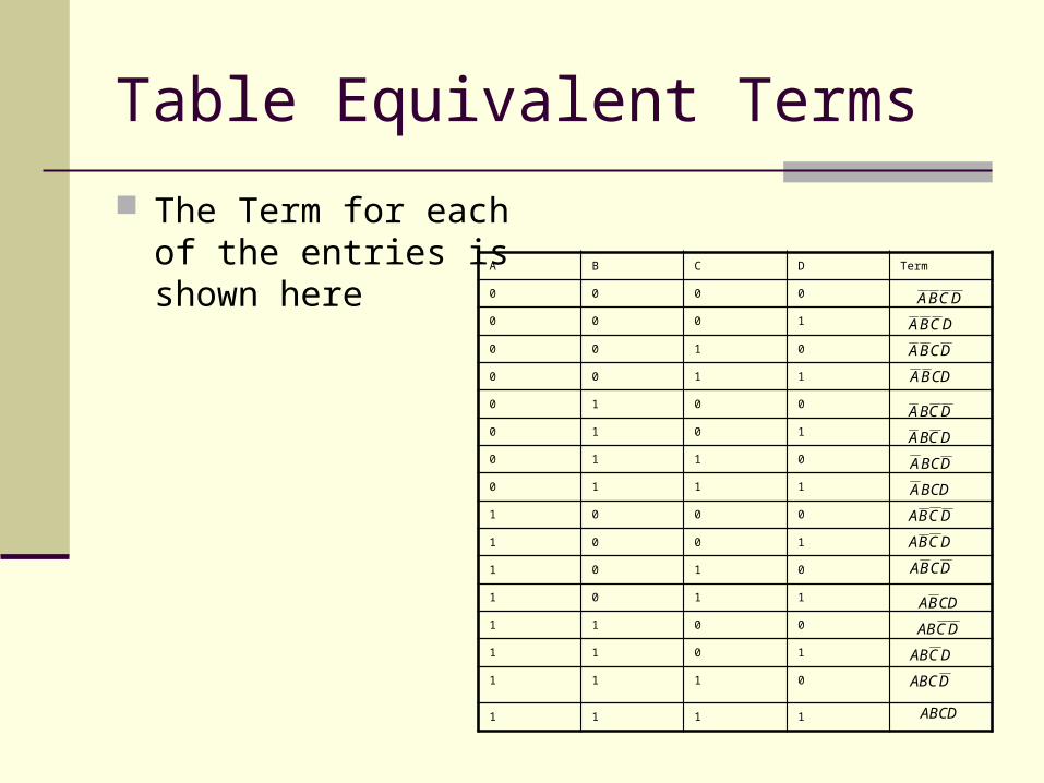
Table Equivalent Terms
The Term for each of the entries is shown here
A B C D Term
0 0 0 0
0 0 0 1
0 0 1 0
0 0 1 1
0 1 0 0
0 1 0 1
0 1 1 0
0 1 1 1
1 0 0 0
1 0 0 1
1 0 1 0
1 0 1 1
1 1 0 0
1 1 0 1
1 1 1 0
1 1 1 1
DCAB
DCAB
DABC
ABCD
CDBA
DCBA
DCBA
DCBA
DCBA
CDBA
DCBA
DCBA
DBCA
BCDA
DCBA
DCBA
Example 1
Write the Equation for the following table
A B C D X
0 0 0 0 0
0 0 0 1 0
0 0 1 0 1
0 0 1 1 1
0 1 0 0 1
0 1 0 1 0
0 1 1 0 0
0 1 1 1 1
1 0 0 0 1
1 0 0 1 0
1 0 1 0 0
1 0 1 1 1
1 1 0 0 1
1 1 0 1 0
1 1 1 0 1
1 1 1 1 0

Comments regarding Example 1
There were 8 – ones in the table, thus there would be 8 terms in the equation
Each one will create exactly one term, that can be easily written by looking at the table and writing the term by looking at the values
Example if you look at the third line of the table A = 0, B=0, C=1, and D=0 and the output is 1. That would generate the term DCBA

Solution to Example 1A B C D X
0 0 0 0 0
0 0 0 1 0
0 0 1 0 1
0 0 1 1 1
0 1 0 0 1
0 1 0 1 0
0 1 1 0 0
0 1 1 1 1
1 0 0 0 1
1 0 0 1 0
1 0 1 0 0
1 0 1 1 1
1 1 0 0 1
1 1 0 1 0
1 1 1 0 1
1 1 1 1 0
DABCDCABCDBADCBABCDADCBACDBADCBAX

Drawing Schematic
Open Altera Quartus II Software File->New->Schematic File Insert Inputs and inverters to create inputs for
AND gates Draw AND gates, selecting appropriate inputs
for each OR the output of the eight AND gates Insert Output

Insert Inputs and Inverters
Draw the following circuit using INPUT and Inverters and draw the wires out ofeach inverter as shown

Name Pins and Nets
As in previous labs name the pins A-D
Click on each wire from the inputs and name them A-D
Click on each wire from the inputs and name them Anot-Dnot

Add AND4 Gates
Insert 8 – AND4 gates (remember one AND gate per term)
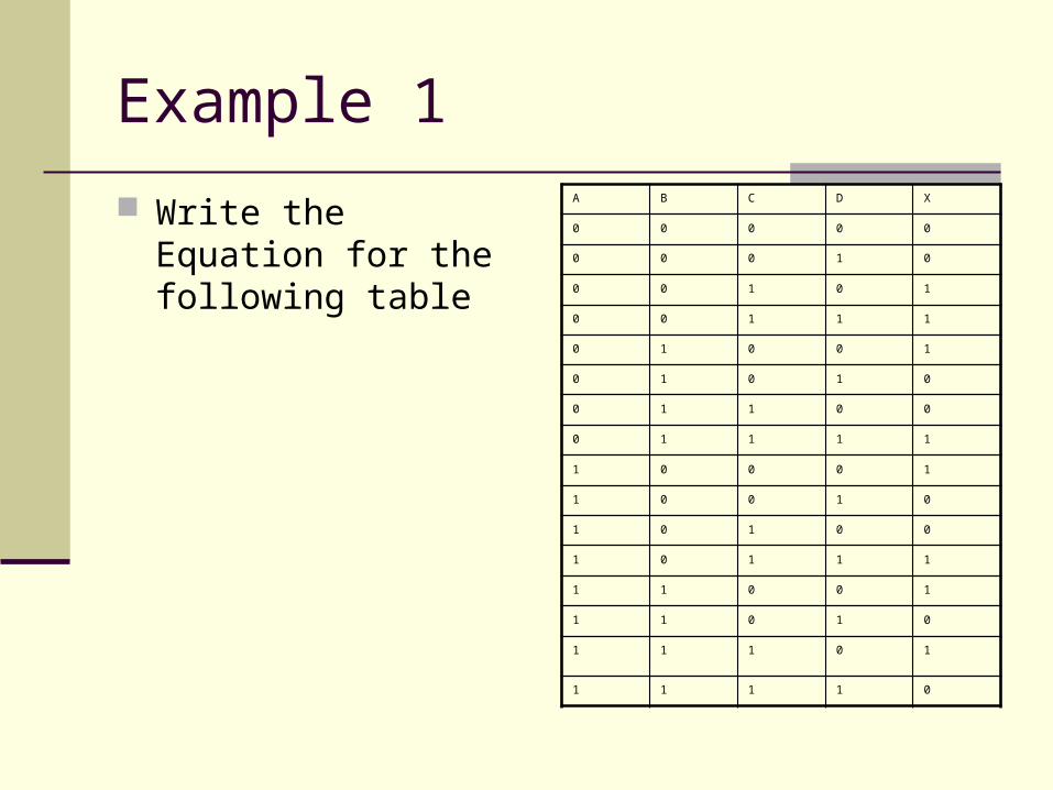
Connect Inputs to AND Gates Connect the four inputs to
the AND gates according to the equation.
This is done by drawing a small wire from each input and naming it as before.
Name them according to the equations from the previous slide
DCABDCABCDBADCBABCDADCBACDBADCBAX

The AND gates Connected

Add OR8 and connect the Product Terms

Insert Output (and name it)

Completed Schematic

Save File
Click this to Create project

Creating the Project -1
First two screens take default and hit next

Device Number
Part Number (EP3C16F484C6N)

Creating the Project – II (Select Device)
Cyclone II Family
Need a specific device
Hit OK when done
EP2C20F484C7 isthe chip on the board
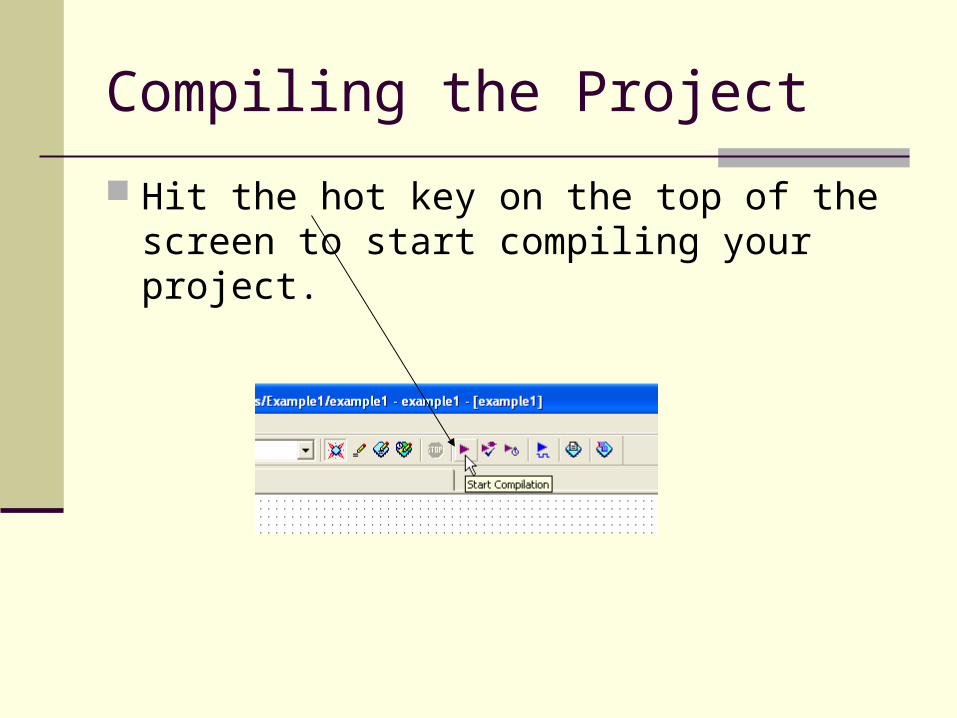
Compiling the Project
Hit the hot key on the top of the screen to start compiling your project.
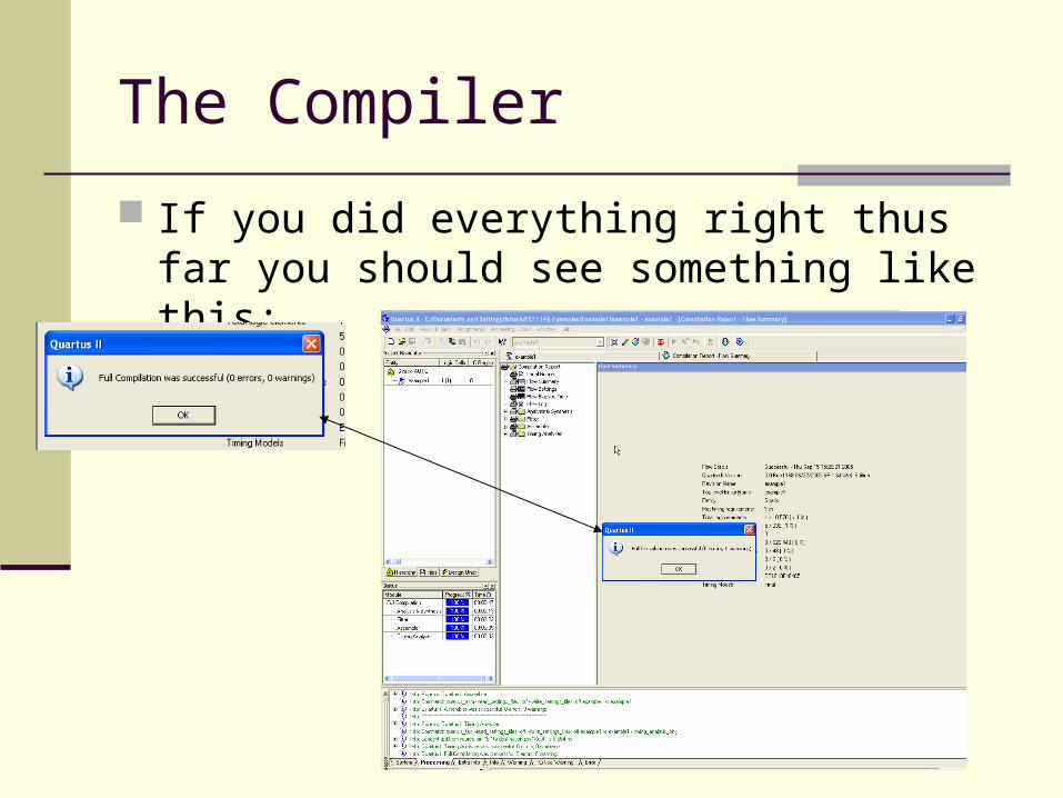
The Compiler
If you did everything right thus far you should see something like this:
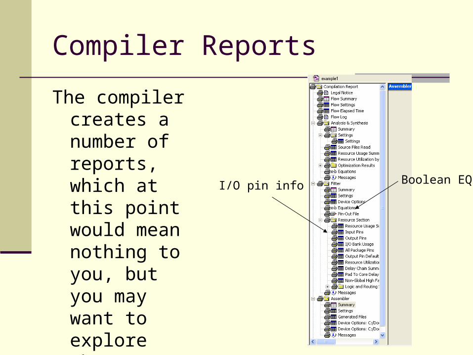
Compiler Reports
The compiler creates a number of reports, which at this point would mean nothing to you, but you may want to explore them.
I/O pin info Boolean EQ
Comments regarding errors
It is very possible that you’ll get errors on this drawing. If so look for two connections on a wire to one of the AND gate inputs. This is the most common error. This often happens on the last AND gate if the wires brought down end at the same point you draw the wire across. Just delete the wire and redraw it.

Assigning Pins - I
Open the Pin Planner to
Assign the pins

Assigning Pins II Look at the data sheet for the
board and determine what your pin numbers need to be.
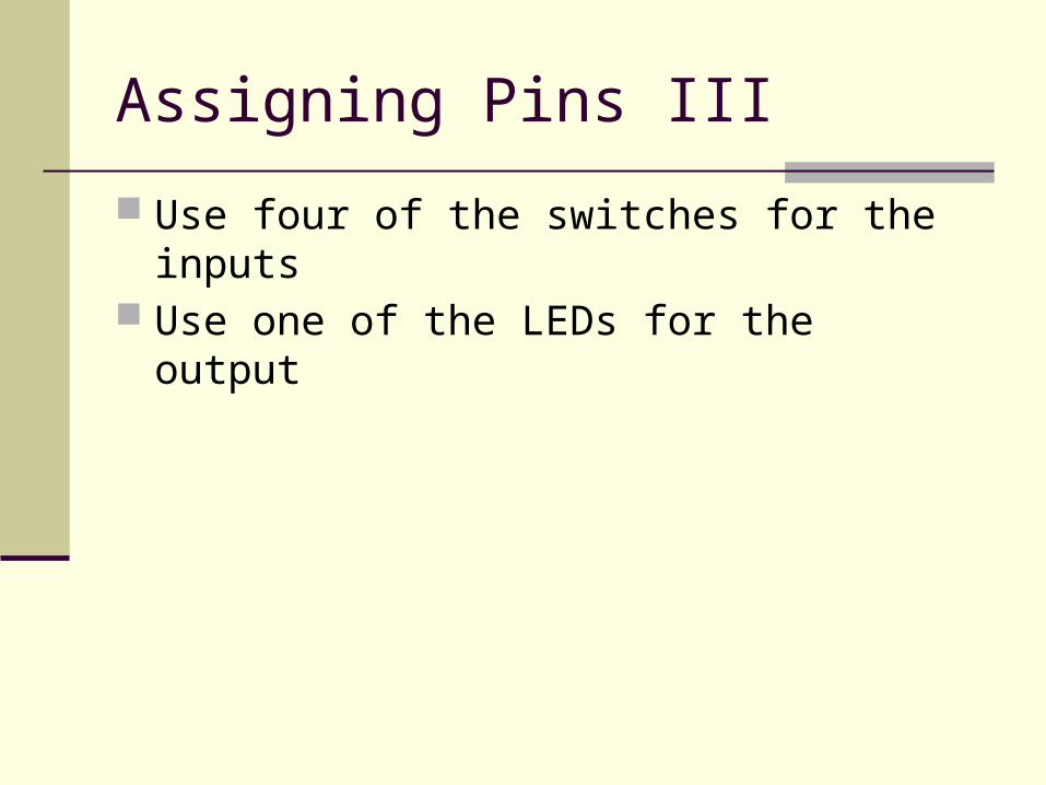
Assigning Pins III
Use four of the switches for the inputs Use one of the LEDs for the output

Assigning the Pins IV

Tristate Unused Pins
Device and Pin Options

Tristate Unused Pins II

Recompile after Assigning Pins and tristating unused pins
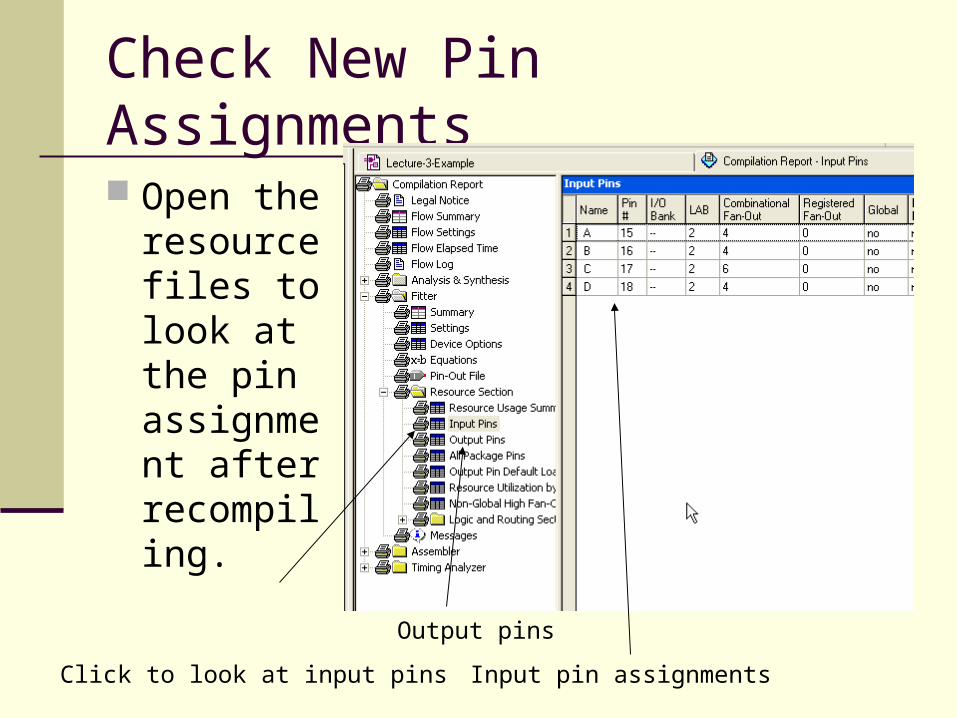
Check New Pin Assignments
Open the resource files to look at the pin assignment after recompiling.
Click to look at input pins Input pin assignments
Output pins
NOTE:
The following slides were copied from Lecture two and the waveforms DO NOT match this example. They are included for instructional purposes only.

Drawing Waveforms for Simulation
We now need to create a new file to hold our simulation input waveforms. This done by hitting new and selecting Other and vector waveform file (vwf)

Entering Nodes
You will need to double click in the node area of the display – this will bring up the following dialog box
Select Node Finder

Entering Nodes II
(1) Start by selecting Pins: all
(2) Then hit List
(3) Move all pins to the rightby hitting >>
(4) Hit OK

Check if all nodes are selected
Verify in the waveform editor that all nodes are shown
Inputs
Output

Change Grid and End Time
Select Edit, Grid time, and change it to 50 nS
Select Edit, End time and change it to 1.6 uS

Grouping Inputs
Select all the inputs, right click, hit ‘Group’ and use inputs[3..0] for the name of the inputs, Hex as radix, and uncheck grey count

Display after Grouping
+ will expand group to show the individual pins- will hide individual pins

Using Count Function
Select the Group, and then hit the count button on the left side of the screen. Take the defaults (start at 0, incr by 1, End value F)

Display after Count
You should see the following after hitting OK

Save Simulation File
Up to now you should have seen that the output is neither high or low. That is because it has not been simulated yet.
In order to simulate you must first save the file as example1.vwf
Leave checked

Simulate
This is the easy part – Hit the simulate button on the top of the screen.
Simulate

Verify Simulation
You should have a value for the output for each input condition.
Manually determine (using techniques from ECET 111) what the output should be for each condition and verify that the output matches that.

Simulation Display

Connect the Altera Board to the PC
Check out an Altera Board from the Lab Tech office

Connect Board to PC I
When checking out board also check out DC wall pack. Ensure that the wall pack is of the correct polarity (+ is the center, - is the outside) and is between 9 and 12 volts.
Also get a Male -> Female DB25 cable to connect between the computer and the PC

Connect to PC II
Notice the location of the connectors used, the other DB25 connector is used for experiments.
DB25 Cable to PC DC Power connector

Open the Programming Module
Select the Programmer Hot Button

Select Programming Hardware
Once the programmer is opened – hit hardware setup
Then select Add Hardware
Selected USB Blaster

Select Programming Options
Select Program/Configure and Verify
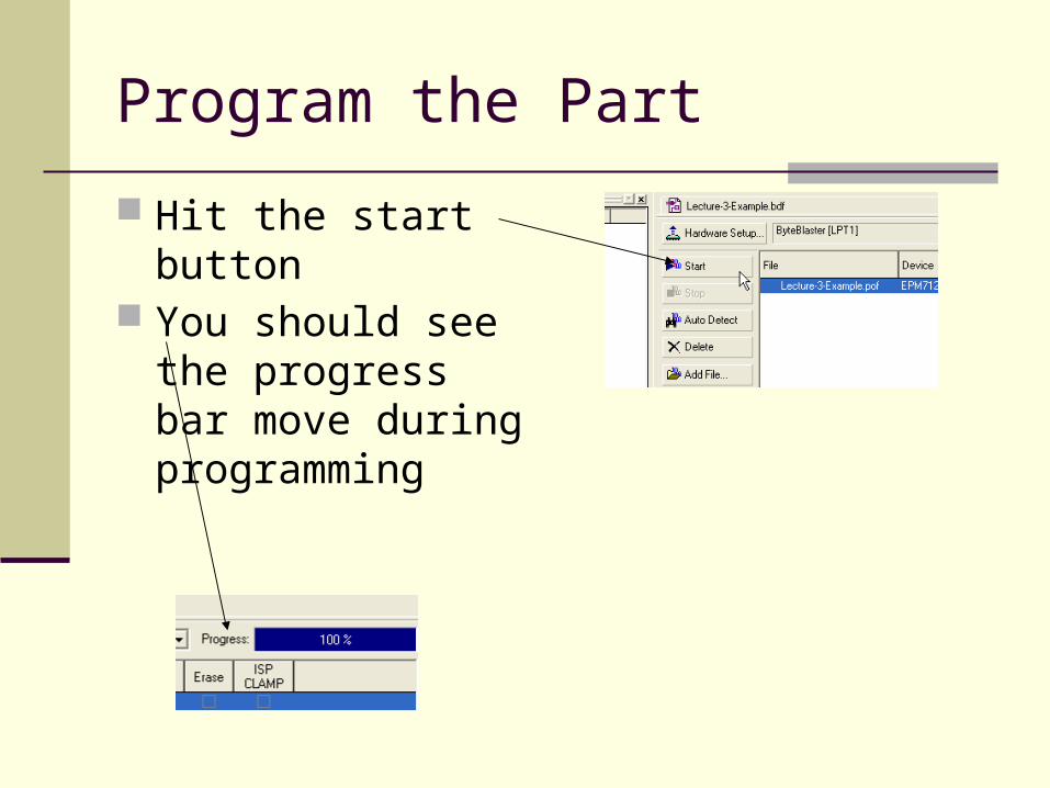
Program the Part
Hit the start button You should see the
progress bar move during programming

Verify the Design
Switch the inputs thru the 16 possible combinations (0000 to 1111) to verify that the design matches the truth table

Summary
This week we covered how to go from any truth table to a schematic very quickly in the Altera software
We also went thru the procedure to specify a device, lock our input/output pins to particular pins and program the device
We also we over how to verify a combinational logic design using the Altera hardware

Lab Two
Design a circuit and verify it using the techniques covered in this week’s lecture that will have the following truth table.
Turn in your printouts from the schematic editor and simulator.
Have myself or the TA initial the schematic to verify that your circuit worked
A B C D X
0 0 0 0 1
0 0 0 1 1
0 0 1 0 0
0 0 1 1 0
0 1 0 0 1
0 1 0 1 0
0 1 1 0 0
0 1 1 1 0
1 0 0 0 0
1 0 0 1 0
1 0 1 0 0
1 0 1 1 0
1 1 0 0 0
1 1 0 1 0
1 1 1 0 1
1 1 1 1 1
Recommended