Page 1266
Adjustable Frequency–Duty-Cycle Hybrid Control Strategy for
Full-Bridge Series Resonant Converters in Electric Vehicle
Chargers
S.Sai Krishna
M.Tech Student
Department of EEE,
Visvodaya Engineering College,
Kavali, S P S R NELLOER,
AP, India-524201.
A.Bhaktha Vachalaa
Associate Professor
Department of EEE,
PBR VITS,
S P S R NELLOER,
AP, India-524201.
Abstract:
In this paper, an effective output voltage control
method using adjustable frequency–duty-cycle hybrid
control is presented. By using the proposed method,
the operating performance of the full-bridge series
resonant dc–dc converter applied to the onboard
charger in electric vehicles under the constant-
voltage charge mode is improved. The proposed
control method improves the system efficiency of the
charger up to 4% for light load conditions compared
with the conventional control method without any
extra hardware. A theoretical analysis is described
along with a loss analysis in detail, and the validity of
the proposed method is verified by experiment with a
3.3-kW prototype onboard charger.
1. Introduction:
For the onboard charger (OBC) installed in plug-in
hybrid electric vehicles (EVs) and pure EVs, high
efficiency and high power density are required to
maximize the energy utilization and the distance
covered per charge. Using resonant converters capable
of soft switching at a high switching frequency is an
effective solution for these requirements. In this
regard, various converter topologies such as series,
parallel, and LLC resonant converters are being
actively adopted on the dc–dc converter for the OBC
in EVs. Among the various charge algorithms for Li-
ion batteries in EVs, it is known that the constant-
current (CC) and constant-voltage (CV) charge
methods are effective and widely applied to the
charger. In the first charging phase, the battery voltage
is gradually increased at a constant current. As soon as
the battery voltage reaches the trickle level, the CV
charge method is applied as the charging current
gradually drops to the maintenance level. It should be
noted here that the CV charge mode controls the low–
medium load range, and its charge time is almost about
40% of the total charge time. Therefore, the efficiency
during the CV charge mode should be improved for
higher energy utilization. For example, in general, a
3.3-kW prototype OBC with a maximum efficiency of
93% could be accomplished by using a full-bridge
series resonant dc–dc converter with the CC–CV
charge algorithm. Unfortunately, this type of charger
has less than 84% efficiency under light load
conditions less than 500 W. Moreover, operation near
300 W is unstable and not well controlled. This is
because the output voltage of the full bridge series
resonant dc–dc converter is controlled by only
adjusting the switching frequency. According to the
impedance variation of the Li-ion battery, the
switching frequency sharply increases from full load to
light load so that the switching losses increase,

Page 1267
resulting in deteriorated system performance. In the
case of a phase-shifted full-bridge converter for an
OBC it cannot ensure zero voltage switching (ZVS)
operation at light loads because of the limitations of
the leakage inductance. Further, the effective duty
cycle for transferring power is reduced because the
switching frequency is fixed for the entire load range.
This power reduction results in a reduction of the
efficiency of the converter for light loads. In the
previous research, to alleviate the problems of ZVS in
the phase-shifted full-bridge converter, a full-bridge
resonant converter with a modified resonant network
has been studied .On the other hand, the use of pulse
width modulation technologies instead of conventional
frequency modulation technology to improve the
efficiency of the resonant converter have been studied.
However, in previous works, only the duty cycles are
changed with fixed switching frequency to control the
output voltage of the half-bridge dc–dc converter. As a
result, the converter cannot be operated under ZVS
condition owing to the limitations of the duty cycle,
leading to a decrease in the efficiency for light loads.
Thus, an effective control method that allows the OBC
to carry out soft switching for a wide range of loads is
required.
2. Literature Survey:
A. Kuperman, U. Levy, J. Goren, A. Zafransky, and A.
Savernin, are proposed that this paper presents the
functionality of a commercialized fast charger for a
lithium-ion electric vehicle propulsion battery. The
device is intended to operate in a battery switch
station, allowing an up-to 1-h recharge of a 25-kWh
depleted battery, removed from a vehicle. The charger
is designed as a dual-stage-controlled ac/dc converter.
The input stage consists of a three-phase full-bridge
diode rectifier combined with a reduced rating shunt
active power filter. The input stage creates an
uncontrolled pulsating dc bus while complying with
the grid codes by regulating the total harmonic
distortion and power factor according to the
predetermined permissible limits. The output stage is
formed by six interleaved groups of two parallel dc-dc
converters, fed by the uncontrolled dc bus and
performing the battery charging process. The charger
is capable of operating in any of the three typical
charging modes: constant current, constant voltage,
and constant power. Extended simulation and
experimental results are shown to demonstrate the
functionality of the device.
A. Hajimiragha, C. A. Cañizares, M. W. Fowler, and
A. Elkamel are proposed that this paper analyzes the
feasibility of optimally utilizing Ontario's grid
potential for charging plug-in hybrid electric vehicles
(PHEVs) during off-peak periods. Based on a
simplified zonal model of Ontario's electricity-
transmission network and a zonal pattern of base-load
generation capacity from 2009 to 2025, an
optimization model is developed to find the optimal, as
well as maximum, penetrations of PHEVs into
Ontario's transport sector. The results of this paper
demonstrate that the present and projected electricity
grid in Ontario can be optimally exploited for charging
almost 6% of the total vehicles in Ontario or 12.5% of
the vehicles in Toronto's transport sector by 2025; this
corresponds to approximately 500 000 PHEVs that can
be charged from the grid without any additional
transmission or power-generation investments beyond
those currently planned.
M. Yilmaz and P. T. Krein are proposed the current
status and implementation of battery chargers,
charging power levels, and infrastructure for plug-in
electric vehicles and hybrids. Charger systems are
categorized into off-board and on-board types with
unidirectional or bidirectional power flow.
Unidirectional charging limits hardware requirements
and simplifies interconnection issues. Bidirectional
charging supports battery energy injection back to the
grid. Typical on-board chargers restrict power because
of weight, space, and cost constraints. They can be
integrated with the electric drive to avoid these
problems. The availability of charging infrastructure
reduces on-board energy storage requirements and
costs. On-board charger systems can be conductive or
inductive. An off-board charger can be designed for
high charging rates and is less constrained by size and

Page 1268
weight. Level 1 (convenience), Level 2 (primary), and
Level 3 (fast) power levels are discussed. Future
aspects such as roadbed charging are presented.
Various power level chargers and infrastructure
configurations are presented, compared, and evaluated
based on amount of power, charging time and location,
cost, equipment, and other factors.
M. G. Egan, D. L. OSullivan, J. G. Hayes, M. J.
Willers, and C. P. Henze, are proposed a novel power-
factor-corrected single-stage alternating current/direct
current converter for inductive charging of electric
vehicle batteries is introduced. The resonant converter
uses the current-source characteristic of the series-
parallel topology to provide power-factor correction
over a wide output power range from zero to full load.
Some design guidelines for this converter are outlined.
An approximate small-signal model of the converter is
also presented. Experimental results verify the
operation of the new converter
J. Y. Lee and H. J. Chae,aresuggests another candidate
for high-power onboard charger for electric vehicles. It
is based on a discontinuous conduction mode (DCM)
power factor correction (PFC) converter with
harmonic modulation technique that improves the
power factor in DCM PFC operation and a two-stage
dc/dc converter composed of a resonant converter and
a DCM buck converter. Separating the functions of the
dc/dc stage into control and isolation helps to reduce
the transformer by using high-frequency resonance.
The feasibility of the proposed charger has been
verified with a 6.6-kW prototype.
3. Proposed System
This paper discusses an adjustable frequency–duty-
cycle (AFDC) hybrid control method in which the duty
cycle and the switching frequency are adjusted
according to load variations to control the output
voltage. Moreover, the effective duty cycles and
switching frequencies for the optimum operating
points that ensure soft switching are induced. The
proposed method improves the operating performance
of the OBC in EVs under light loads without additional
hardware. Based on the analytical results, accurate
duty cycles available for ZVS operation are estimated
for load variations. Then, the loss analyses of the
major components such as semiconductors, the
transformer, and the resonant inductor are performed.
Finally,the overall performance of the proposed
control method is verified by experiment with a 3.3-
kW prototype OBC.
A. Operational Characteristics of AFDC Hybrid
Control
To compensate the performance degradation problem
under light loads in the CV charge mode, the switching
frequency should be reduced. As shown in Fig. 1(b)
and (1), the inputto-output voltage gain can be
characterized by dividing the ac equivalent resistance
Rac by the total impedance of the resonant network
Zin. Zin increases with an increase in the switching
Fig. 3. Steady-state operating waveforms of AFDC
hybrid control. Frequency above the resonance
frequency.
Page 1269
Under conventional frequency control with D = 0.5,
the RMS value of the square wave voltage applied to
the resonant network is constant. Therefore, Zin should
increase according to the load reduction to maintain
the voltage ratio at a constant value. Implicit in this
voltage relationship is the fact that the output voltage
can be maintained constant provided the value of the
total impedance and the RMS value of the square-
wave input voltage of the resonant network are
appropriately adjusted according to the load reduction.
The main concept of the proposed AFDC hybrid
control is as follows. The RMS value of the square-
wave input voltage of the resonant network can be
reduced by changing the duty cycle. On the other hand,
the value of the total impedance can be minimized by
reducing the switching frequency because the resonant
network impedance is a function of the switching
frequency. This implies that the converter can be
operated at lower switching frequencies than the
switching frequencies of the conventional control
method for light loads. Thus, it is important to analyze
the relationship between the duty cycle and the
switching frequency for efficient operation of the
converter. Fig. 3 shows the steady-state operating
waveforms of the converter by AFDC hybrid control
for an arbitrary CV charge mode. In the operating
waveforms in Fig. 3, the time variation and the phase
of the hth-order harmonic of vdare respectively given
by
The dc component of the square-wave voltage vdis
blocked by the series resonant capacitor Cr; thus, the
ac component of vdforces the resonant current irto
flow through the resonant network. The ac component
of vdis given by
The RMS value of the square-wave voltage, which
contributes to the transfer of active power to the load,
can be calculated by applying harmonic components.
Therefore, the RMS voltage Vdis expressed as
The secondary-side voltage of the transformer is
clamped to the output voltage Vo; hence, the RMS
value of the voltage across the ac equivalent resistance
in Fig. 1(b) is represented as nVo. The RMS voltage of
the resonant network input to the RMS voltage
reflected to the primary side is expressed by using
Kirchoff’s voltage law, i.e.,
whereZin represents the total impedance of the hth-
order harmonic of the resonant network, i.e.,
Therefore, the input dc source to the output voltage
gain for the proposed AFDC hybrid control is derived
by substituting (6) into (7) as follows:
Equation (9) is simplified for the voltage gain of the
converter with consideration of the fundamental RMS
value by the filtering action of the Lr− Cr resonant
network as follows:

Page 1270
Fig. 4 shows the voltage gains according to the
variation in ωnfor various values of D for n = 0.73 at
100% and 30% loads. As shown in Fig. 4, the decrease
in the duty cycle reduces the input–output voltage gain
at the same frequency.
On the other hand, it is observed that the switching
frequency decreases with a reduction of the duty cycle
while maintaining the same input–output voltage gain.
In particular, the decrease in the switching frequency is
distinguishable for light loads. This implies that the
decrease in the switching frequency can alleviate the
switching losses and eventually enhance the converter
efficiency.
Fig. 4. Voltage gain as a function of ωnfor different
duty cycles D. (a) 100% load. (b) 30% load.
The full-bridge series resonant dc–dc converter applied
to the developed 3.3-kW prototype OBC has the
following specifications: maximum output power Po =
3.3 kW, input dc voltage Vin = 380 V, output voltage
Vo = 400 V, resonant inductance Lr= 75 μH, resonant
capacitor Cr = 66 nF, and transformer turns ratio n(=
N1/N2) = 19/26. Thus, it is necessary to determine the
range of duty cycles available for load variations
during the CV charge mode. The equation for the
useable duty cycle is derived from (10) and is given by
It is shown in (11) that D is a function of Q and
ωnwith the given parameters Vo, Vin, and n.
Therefore, D can be expressed according to the
frequency variations with respect to each load. Fig. 5
shows the theoretically adjustable duty cycle for Vo=
400 V. As shown in Fig. 5, the switching frequency
should be varied by about 4.4 times the resonant
frequency to obtain the same output voltage as the load
is changed from 100% to 10% for D = 0.5. On the
other hand, a smaller duty cycle at the same load
means that the switching frequency is smaller.
Moreover, It can be seen that the frequency variation is
definitely small compared with D = 0.5 as the load
changes from 100% to 10%. This implies that the
switching frequency can be decreased by reducing the
duty cycle because the load is smaller during the CV
charge mode. Switching losses can be
Fig. 5. Theoretically adjustable duty cycles for load
variations for the given parameters.
dramatically minimized at turn off by the decreased
switching frequencies. Theoretically, the duty cycle
can be reduced by a factor of 0.33 to maintain the
Page 1271
output voltage at 400 V in the range of loads
considered for the developed 3.3-kW prototype OBC.
B. Estimation of the ZVS Operation Range
Guaranteeing the ZVS range is a key aspect for
operating resonant converters. Therefore, it is
important to estimate the duty cycles corresponding to
the switching frequencies that ensure the ZVS range to
improve the decreased efficiencies due to increased
switching frequencies in the CV charge mode. During
operation, each of the fundamental and harmonic
voltage components given by (5) produces
fundamental and harmonic currents through the series
resonant network. In conventional frequency control
with D = 0.5, the positive resonant current flowing
through the resonant network is always symmetrical to
the negative resonant current because the phase of the
fundamental voltage is in phase with that of the hth-
order harmonic voltage. This implies that each switch
is turned off under the same current conditions. As
shown by (4), however, the phases of the fundamental
and harmonic voltages vary according to D. This is
different from the hth-order harmonics and leads to an
asymmetrical resonant current. Accordingly, switches
(SW1−SW4) are turned off under different current
conditions. The time-varying resonant current through
the resonant networks derived from (5) and given by
whereϕh represents the phase delay of the hth-order
harmonic between vdac and ir, as given by
Normally, the condition for ZVS operation in all
switches is represented from (4) and (13) as follows
[14]:
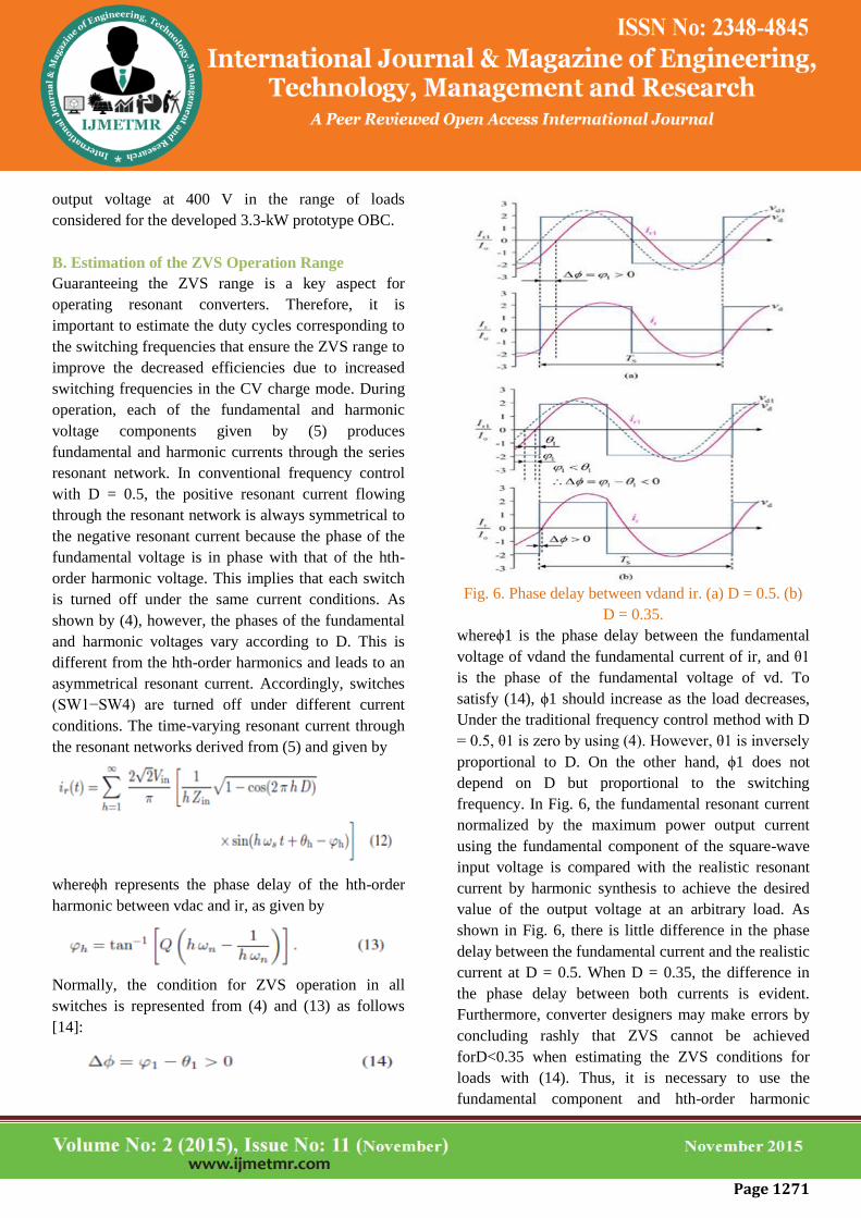
Fig. 6. Phase delay between vdand ir. (a) D = 0.5. (b)
D = 0.35.
whereϕ1 is the phase delay between the fundamental
voltage of vdand the fundamental current of ir, and θ1
is the phase of the fundamental voltage of vd. To
satisfy (14), ϕ1 should increase as the load decreases,
Under the traditional frequency control method with D
= 0.5, θ1 is zero by using (4). However, θ1 is inversely
proportional to D. On the other hand, ϕ1 does not
depend on D but proportional to the switching
frequency. In Fig. 6, the fundamental resonant current
normalized by the maximum power output current
using the fundamental component of the square-wave
input voltage is compared with the realistic resonant
current by harmonic synthesis to achieve the desired
value of the output voltage at an arbitrary load. As
shown in Fig. 6, there is little difference in the phase
delay between the fundamental current and the realistic
current at D = 0.5. When D = 0.35, the difference in
the phase delay between both currents is evident.
Furthermore, converter designers may make errors by
concluding rashly that ZVS cannot be achieved
forD<0.35 when estimating the ZVS conditions for
loads with (14). Thus, it is necessary to use the
fundamental component and hth-order harmonic

Page 1272
components for more exact analysis for asymmetrical
duty cycle control, particularly when investigating the
ZVS range.
As can be seen from the steady-state operating
waveforms, the current of switches SW1 and SW2 at
turn off causes the antiparallel diodes of switches SW3
and SW4 to conduct prior to the turn on of SW3 and
SW4. Similarly, the operation of switches SW1 and
SW2 is caused by the turn off of switches SW3 and
SW4. Consequently, the turn-off currents provide
information on whether the switches (SW1 − SW4) are
turned on under ZVS conditions [9]. The values of
currents ISW1, 2 and ISW3, 4 are defined at DTS and
TS, respectively, and are given by
By energy balance of the resonant network, the value
of ISW1, 2 at turn off increases as the turn-on time
DTS of switches SW1 and SW2 decreases; thus,
switches SW3 and SW4 are sure to be turned on under
zero voltage for various loads. In contrast, the absolute
value of ISW3, 4 at the end of the switching period TS
is smaller. Furthermore, because the drain–source
capacitor Coss exists in parallel with the switch, ISW3,
4 should exceed the minimum value necessary to
completely charge/discharge Coss within the dead time
td to guarantee ZVS. Assuming the overall capacitor
Cs(= 2Coss)is in parallel with every switch of the full-
bridge converter, the minimum value of ISW3, 4 is
defined as
Determination of the ZVS ranges of all switches by
investigating whether the value calculated from (16)
satisfies the necessary requirements of (17) and (19)
for various loads is very adequate. Fig. 7 shows the
effective duty cycles available for various loads
corresponding to each switching frequency for Vo=
400 V during the CV charge mode. As shown in Fig.
7(a) and (b), the analysis using harmonic
decomposition offers more exact information about the
ZVS ranges. This implies that the turn-off switching
losses can be alleviated as the converter is operated
along the red dotted line, which indicates the optimum
operation points, for various loads.
Fig. 7. Effective duty cycles according to load for Vo=
400 V. (a) First harmonic approximation analysis. (b)
Harmonic analysis.
IV. LOSS ANALYSIS
Here, a loss analysis is carried out to predict the
efficiency. In this paper, the main sources of loss are
analyzed, neglecting the parasitic components such as
stray inductances and capacitance on the basis of the
simulation results and calculated values in the previous

Page 1273
sections. Analysis of the main sources is sufficient to
understand the effect of AFDC hybrid control on
losses.
The main sources of loss include the following: 1)
transformer/resonant inductor loss (iron/winding loss);
2)MOSEFT conduction loss and switching loss; and 3)
MOSFET body/rectifying diode conduction loss. The
main components applied to the 3.3-kW prototype full-
bridge series resonant dc–dc converter for loss analysis
are summarized in Table II. Magnetic Component
Losses: Transformer and inductor losses can be
classified into two major categories: iron loss
Fig. 8. Magnetic flux density and iron loss distribution
of the transformer for Po = 300 W.
Fig. 9. Loss distributions versus Po. (a) Conventional
frequency control. (b) AFDC hybrid control.
and winding loss. Among them, the winding loss
considers the winding dc resistance. Skin effect losses
can be prevented for the most part by utilizing Litz
wire. Iron losses have a complex distribution because
they depend on the magnetic flux density distribution
that accounts for the core magnetic saturation.
Moreover, the magnetic flube differently distributed
unlike that by conventional frequency control with D =
0.5. Asymmetrical current can lead to partial core
saturation; therefore, it is necessary to predict the
distribution precisely. A magnetic field analysis
simulation based on a finite-element method (FEM)
using JMAG-Designer v11.1 is carried out to evaluate
the complex magnetic flux distributions of the
transformer and inductor core. The magnetic flux
density and iron loss distributions of the transformer
between D = 0.5 and D = 0.3 at Po = 300 W are
presented in Fig. 8. As shown in Fig. 8, the value of
the maximum flux density for D = 0.3 is about three
times larger than that for D = 0.5, increasing the iron
loss of the transformer. This is due to asymmetrical
currents and higher harmonic frequencies.
Semiconductor Losses:
The switch conduction losses are calculated by the
MOSFET approximation with the drain–source ON-
state resistance. Because MOSFETs operate at ZVS
conditions, only the turn-off loss is considered and not
the turn-on loss. The conduction losses of the ant
parallel diodes and the full-bridge rectifying diodes are
calculated by using the diode approximation with the
diode ON-state voltage under the zero-current
condition, the diode ON-state resistance, and the diode
current.
Efficiency Estimation:
The efficiency of the full-bridge series resonant dc–dc
converter is predicted by using the loss results
analyzed earlier. The loss distributions of conventional
frequency control and AFDC hybrid control are
compared in Fig. 9. Although AFDC hybrid control
leads to increasing transformer losses, they comprise a
small part of the total losses. On the other hand,
because the switching frequency for conventional

Page 1274
frequency control is much higher than that of the
proposed control, the converter suffers from increased
switching loss and iron loss of the resonant inductor.
These indicate that the MOSFETs and the inductor are
the dominant sources of power losses.
Software Requirement
While coming to the software part here we are
usingmatlab software which will be use to simulating
the given code in blocks.
Block Diagram of VFD System
FIG: VFD System
4. Results:
Simulation Results
Electric Vehicle (1)
Electric Vehicle (2)
Electric Vehicle (3)
Electric vehicle (4)
Conclusion:
An effective frequency modulation technique that
adjusts the duty cycle for loads was proposed to
increase the efficiency of the full-bridge series
resonant dc–dc converter in the OBC for light loads.
The optimum operation points allowing ZVS operation
for a wide range of loads were theoretically analyzed
in detail. To investigate the effect of AFDC hybrid
control on the losses of the components, the losses of
the primary components were calculated. In addition,
the loss distributions of the magnetic components were
estimated more precisely by utilizing a magnetic field
analysis simulation tool based on a finite-element
method (FEM). For verification of the proposed
control method, the developed 3.3-kW full-bridge
series resonant dc–dc converter was used. At different
duty cycles, the experimental efficiency of the
proposed method was compared with that of the
conventional control method. The analytical and
experimental results showed that the proposed control
method improved the efficiency of the converter by a
maximum of 4% for light loads without any extra
hardware.
Page 1275
REFERENCES
[1] A. Kuperman, U. Levy, J. Goren, A. Zafransky,
and A. Savernin, “Battery charger for electric vehicle
traction battery switch station,” IEEE
Trans.Ind.Electron., vol. 60, no. 12, pp. 5391–5399,
Dec. 2013.
[2] A. Hajimiragha, C. A. Cañizares, M. W. Fowler,
and A. Elkamel, “Optimal transition to plug-in hybrid
electric vehicles in Ontario, Canada, considering the
electricity-grid limitations,” IEEE Trans. Ind.
Electron.,vol. 57, no. 2, pp. 690–701, Feb. 2010.
[3] M. Yilmaz and P. T. Krein, “Review of battery
charger topologies, charging power levels, and
infrastructure for plug-in electric and hybrid
vehicles,”IEEE Trans. Power Electron., vol. 28, no. 5,
pp. 2151–2169,May 2013.
[4] M. G. Egan, D. L. OSullivan, J. G. Hayes, M. J.
Willers, and C. P. Henze, “Power-factor-corrected
single-stage inductive charger for electric vehicle
batteries,” IEEE Trans. Ind. Electron., vol. 54, no. 2,
pp. 1217–1226,Apr. 2007.
[5] J. Y. Lee and H. J. Chae, “6.6-kW onboard charger
design using DCM PFC converter with harmonic
modulation technique and two-stage DC/DC
converter,” IEEE Trans. Ind. Electron., vol. 61, no. 3,
pp. 1243– 1252, Mar. 2014.
[6] B. Y. Chen and Y. S. Lai, “New digital-controlled
technique for battery charger with constant current and
voltage control without current feedback,” IEEE
Trans. Ind. Electron., vol. 59, no. 3, pp. 1545–
1553,Mar. 2012.
[7] D. S. Gautam, F. Musavi, M. Edington, W. Eberle,
and W. G. Dunford, “An automotive onboard 3.3-kW
battery charger for PHEV application,”IEEE Trans.
Veh. Technol., vol. 61, no. 8, pp. 3466–3474, Oct.
2012.
[8] D. Czarkowski and M. K. Kazimierczuk, “Single-
capacitor phasecontrolled series resonant converter,”
IEEE Trans. Circuits Syst. I,Fundam. Theory Appl.,
vol. 40, no. 6, pp. 383–391, Jun. 1993.
[9] P. K. Jain, A. St-Martin, and G. Edwards,
“Asymmetrical pulse-widthmodulated resonant
DC/DC converter topologies,” IEEE Trans. Power
Electron., vol. 11, no. 3, pp. 413–422, May 1996.
[10] F. S. Pai, C. L. Ou, and S. J. Huang, “Plasma-
driven system circuit design with asymmetrical
pulsewidth modulation scheme,” IEEE Trans.
Ind.Electron., vol. 58, no. 9, pp. 4167–4174, Sep.
2011.
[11] B. C. Kim, K. B. Park, and G. W. Moon,
“Asymmetric PWM control scheme during hold-up
time for LLC resonant converter,” IEEE Trans.Ind.
Electron., vol. 59, no. 7, pp. 2992–2997, Jul. 2012.
[12] H. S. Kim, J. H. Jung, J. W. Baek, and H. J. Kim,
“Analysis and design of a multioutput converter using
asymmetrical PWM half-bridge flyback converter
employing a parallel-series transformer,” IEEE Trans.
Ind. Electron.,vol. 60, no. 8, pp. 3115–3125, Aug.
2013.
Author Details:
A.Bhaktha Vachala received the B.Tech. degree from
PBR VITS in the year 2003 and M.Tech degree from
the JNTU, Hyderabad, India. Also Perusing Ph.D.
degree from Jawaharlal Nehru Technological
University, Hyderabad. He is working in the area of
Electric vehicle applications in transportation systems
from last four years. He has been with the Department
of Electrical and Electronics Engineering, PBR
Visvodaya Institute of Technology and Science, Kavali
affiliated by JNTU Anatapur since last 10years, where
he is currently an Associate Professor. His research
interests include several areas of power electronics and
electric vehicle applications of power electronics. He
has authored or coauthored several papers in power

Page 1276
electronics. He holds a UGC sponsored project worth
of 4,60,00/-.
S. Sai Krishna received the B.Tech degree from Sree
Institute of Technical Education in the year 2012. And
pursuing M.Tech in Visvodaya Engineering College in
Kavali.
Recommended