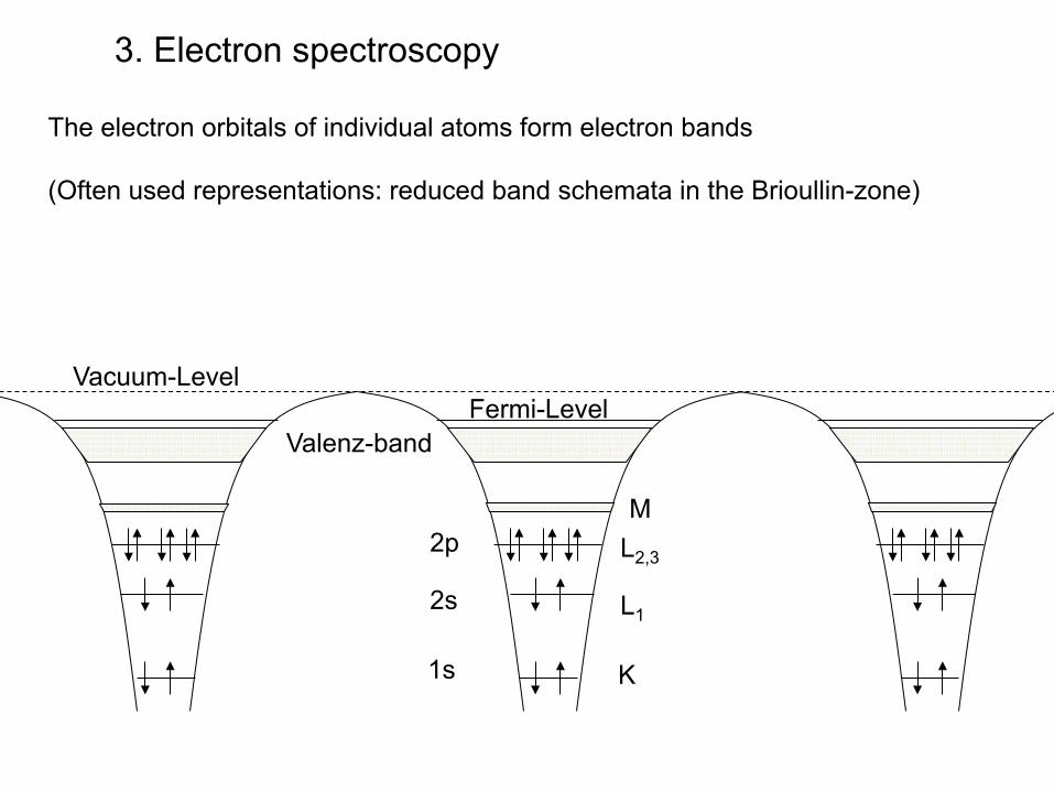
3. Electron spectroscopy
1s
2s
2p
K
L1
L2,3
M
Valenz-band Fermi-Level
Vacuum-Level
The electron orbitals of individual atoms form electron bands (Often used representations: reduced band schemata in the Brioullin-zone)
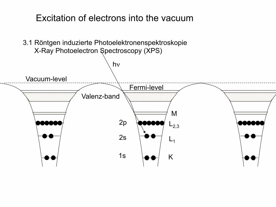
Excitation of electrons into the vacuum
1s
2s
2p
K
L1
L2,3
M
Valenz-band Fermi-level
Vacuum-level
3.1 Röntgen induzierte Photoelektronenspektroskopie X-Ray Photoelectron Spectroscopy (XPS)
hν

Excitation of electrons into the vacuum
1s
2s
2p
K
L1
L2,3
M
Valenz-band Fermi-level
Vakuum-level
3.2 Auger-Electron Spectroscospy (AES)
hν or e-
MPI für Metallforschung ZWE Dünnschicht labor
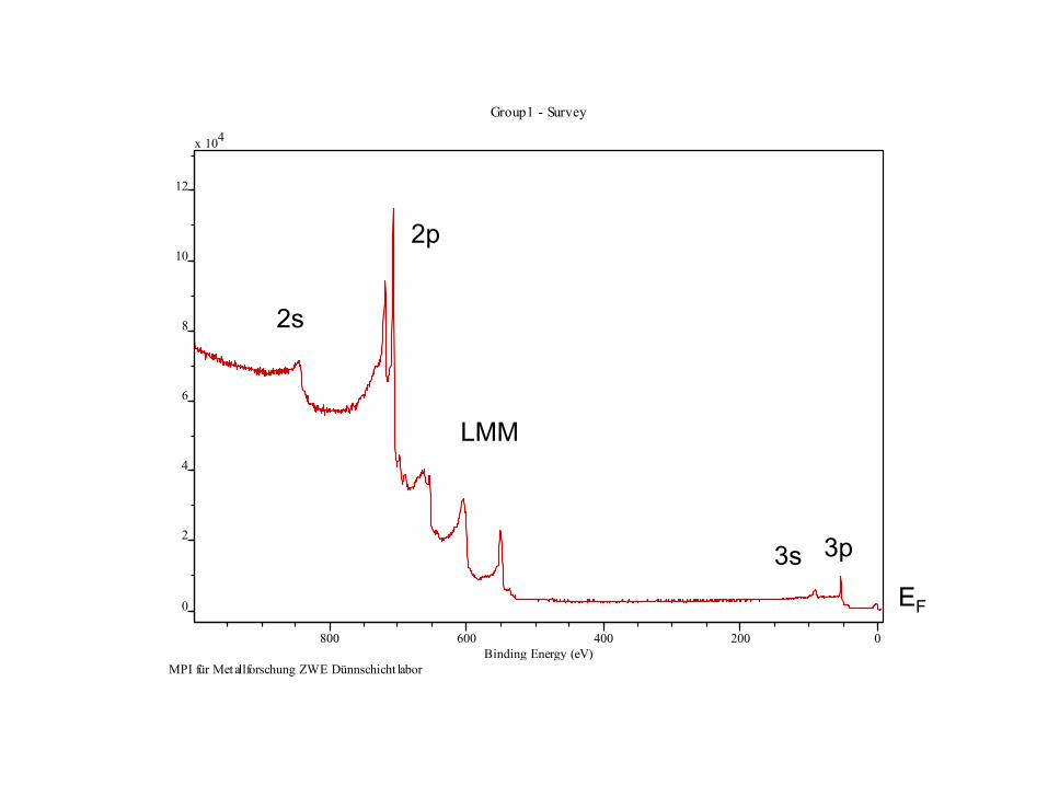
Group1 - Survey
x 104
0
2
4
6
8
10
12
CPS
800 600 400 200 0Binding Energy (eV)
2s
2p
3s 3p
LMM
EF

Finger print analysis
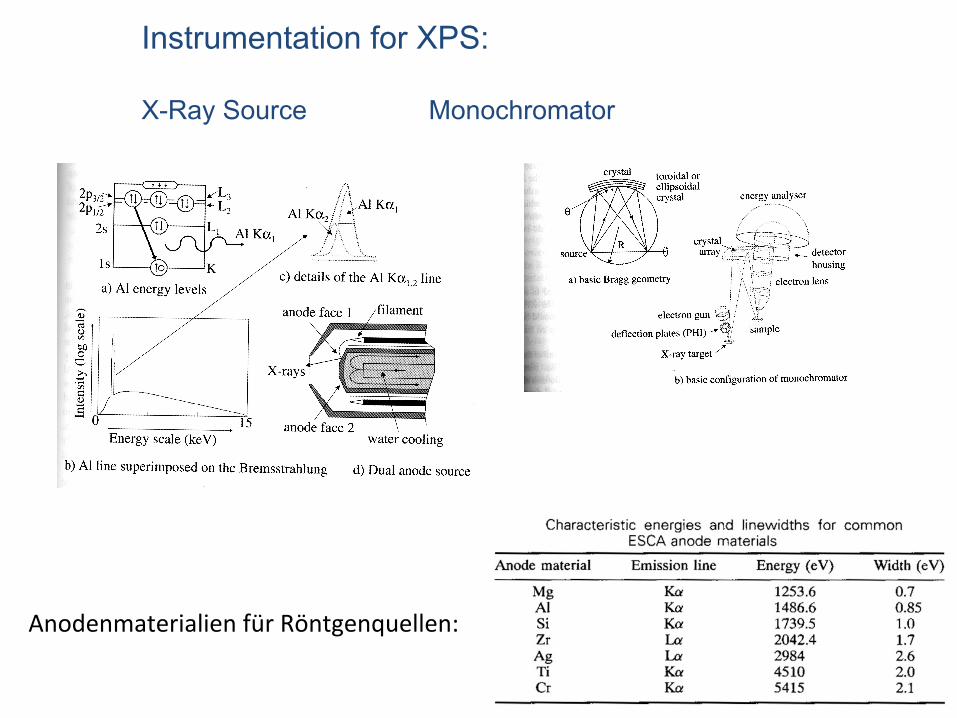
Instrumentation for XPS: X-Ray Source Monochromator
Anodenmaterialien für Röntgenquellen:

Electrone-detector:
Electrostatic hemispherical analyzer (HAS)
Double pass cylindrical mirror analyzer (DPCMA)
Energy resolution for HAS:
0
20
2rrw
EE α+=
Δ
w: slit width, α: convergence angle of photo electron “beam”
Elektronenvervielfacher in Verwendung

• Binding energy, effect of chemical binding - Comparison of initial and final state of atom (difference in energy)
EB = Ef(n-1) - Ei(n)
EB: Bindungsenergie; Ei: Energie des Atoms im Anfangszustand; Ef: Energie des Atoms im Endzustand; n: Anzahl der Elektronen - Without reorganisation of the electrons: EB = - εk
εk: Orbitalenergie - Relaxations due to electron loss:
EB = - εk + Er(k)
Er(k): Relaxationsenergie
• Effect of initial state: - Change of EB due to change in chemical binding
• example: oxydization leads to increase of EB by ΔEB
ΔEB = - Δεk

(a) Verschiebung des S1s Peaks als Funktion des Oxidations- zustandes für verschiedene Verbindungen
(b) S2p Bindungsenergie für verschiedene Schwefelverbindungen als Funktion der berechneten Ladung
Korrelation zwischen Ladung des Atoms und der Bindungsenergie
Chemical Shift:
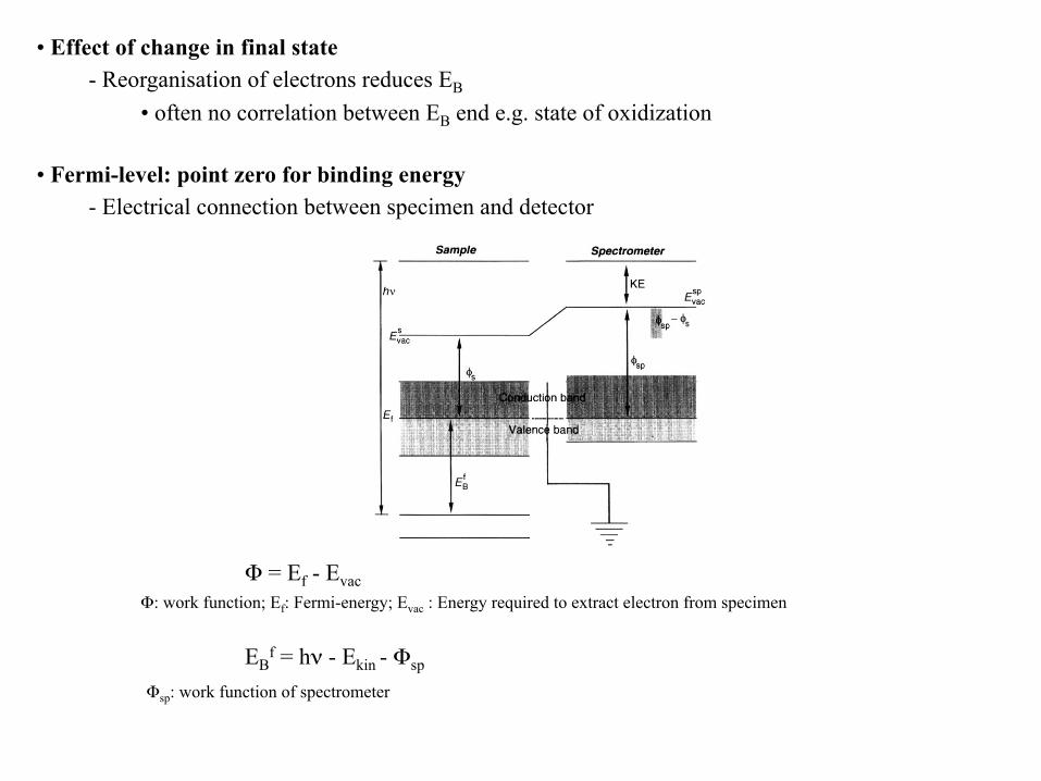
• Effect of change in final state - Reorganisation of electrons reduces EB
• often no correlation between EB end e.g. state of oxidization
• Fermi-level: point zero for binding energy - Electrical connection between specimen and detector
Φ = Ef - Evac Φ: work function; Ef: Fermi-energy; Evac : Energy required to extract electron from specimen
EBf = hν - Ekin - Φsp
Φsp: work function of spectrometer
MPI für Metallforschung ZWE Dünnschicht labor
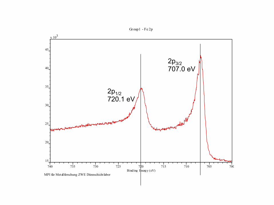
Group1 - Fe 2p
x 103
15
20
25
30
35
40
45
CPS
740 735 730 725 720 715 710 705 700Binding Energy (eV)
2p1/2 720.1 eV
2p3/2 707.0 eV

450 455 460 465 470 1500
2000
2500
3000
3500
4000
4500
Binding Energy (eV)
c/s
Ti4+
Ti2p1/2 Ti2p3/2
Ti3+ + Ti2+
XPS Spektrum einer SrTiO3 Oberfläche
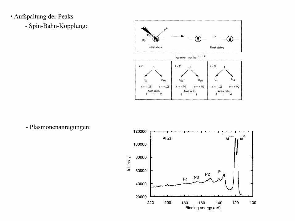
• Aufspaltung der Peaks - Spin-Bahn-Kopplung:
- Plasmonenanregungen:

Max-Planck-Institut für Metallforschung; ZWE Dünnschichtlabor
Pr:Einbau - Au_4f
Arbitrary U
nits
100 98 96 94 92 90 88 86 84 82 80Binding Energy (eV)
ΔE= 1.0 eV
Mg kα XPS Si 2p
Au 4f7/2 Au 4f5/2
as derived
650°C
700°C
750°C
800°C
• Au and Si form eutectica (chemical shift) • evaporation at T > 750°C ⇒ Nano structuring of surface
DCA-‐MBE: Au/SiOx/Si Surfaces
Beri Mnbekum, Department Spatz

Auger-‐Electron-‐Spectroskopy (AES) General remarks
• AES based on excitaOon of electrons and their detecOon • one of the most common used method for chemical analysis of surfaces • ExcitaOon of Auger-‐Electrons by photons or primary electrons • Energy of primary electrons: 3...30 keV • InformaOon on chemical composiOon up to 10 mono layers (ML)
• typical energy range of AES: up to 3 keV

Basiscs of AES: Energy defined by quantum state of electrons:
Kine=c energy of Auger-‐Electrons -‐ Up to three electrons are required in AES; the kineOc energy is defined by:
z.B. EWXY = EK - EL - EV - ΦA EWXY: kineOsche Energie des Auger-‐Elektrons; EK, EL : Energie der entsprechenden Schale
ΦA: Austri^sarbeit des Analysators

Overview AES-Process
Auger-Prozess: EF ist die Fermienergie, Φe und ΦA sind die Austrittsarbeiten der Probe und des Analysators
EWXY = EW(Z)- EX (Z +Δ) - EY (Z + Δ) - ΦA
- Correction Δ for „missing“ electrons:increase of binding energy due to ionization Δ : 0...1

Auger-Transitions as function of the kinetic energy of the elements Z > 2

• cross section σW for ionization for AES Depending on the probability of all processes (excitation of one electron, transition of electron from high orbital to lower, excitation of Auger electron) Quanten mechanic calculations (e.g. Bethe): σW = C ln(cEP/Ew)/(EPEW) EP: Energy of primary electron; EW : Energy of orbital; C: Constant
Experimentelle und berechnete Werte für σW

• Comparison Photom- or Auger-Emission - Energy difference ΔE = EW - EX can be used for emission of x-ray or electron - Quantum mechanical calculation for both processes:
• Back scattering of electrons: - Different processes contribute to the emission of Auger electrons or photons - e.g. back scattered electrons excite Auger electrons:
Itotal = I0 + IM = I0 (1 + rM ) rM: Rückstreufaktor ist Funktion von Z (Atomzahl)
- Approximations for rM 1 + rM = 1 + 2,8 [1 - 0,9 (Ew/Ep)]η(Z) η(Z) = -0,0254 + 0,16 Z - 0,00186 Z2 + 8,3 × 10⁻⁷ Z3
Auger-Elektron (A) Photon (X)

Elektronenrückstreufaktor als Funktion der kinetischen Energie (Ep = 5 keV, θ = 30°)
Auger-Übergänge und relative Intensitätsfaktoren

• Depth of electrons Λ - Elcectrons have mean free path λel
Λ = λel cos θ
Approximation λel = 0,41 a1,5 Ekin0,5
a: thickness of a mono layer (nm)
Ekin (eV), λ (nm)
• Chemical Shift - Shift of Auger-Peaks due to changes in the chemical binding
(change of the electronic structure of the material) - Additional peaks appear
3 2 0 3 4 0 3 6 0 3 8 0 4 0 0 4 2 0 4 4 0 4 6 0 4 8 0
T!i! !O!
T!i!O!
T!i!(!L!M!V!)!
T!i!(!L!M!M!)!
E!k!i!n! !(!e!V!)!
2!
2! 3!
Ti!
d/dE
[EN(E)]
0 . 2 n m T i
0 . 1 n m T i
0 n m T i
E k i n ( e V )
T i ( M V V )
A l ( L V V )
A l ( L V V )
A l ( L 2 , 3 ) O ( L 2 , 3 ) O ( L 2 , 3 )̀
2 0 3 0 4 0 5 0 6 0 7 0
d/dE
{EN
(E)}
Ekin (eV)

Apparatus - Electron gun - Energy Analyser - UHV chamber - Ion gun (for depth profiling) - Detector for surface imaging

• Elektronenquellen - W-Filament Strahlfleck 3...5 µm - LaB6 Kristall < 20 nm - Feldemissionskathode < 20 nm - Strahlenschädigung bei Stromdichten über 1 mA/cm2 (1 nA/10 µm2)

• Aufnahme des Spektrums - Punktanalyse - Linienprofil oder „Mapping“ - Tiefenprofilanalyse
• direktes Spektrum oder differenziertes Spektrum
Prinzip der Ermittlung der chemischen Konzentration einer Schicht in der Tiefe: (a) für Schichten mit Dicken unter 2...3 nm; (b) Schichtdicke < 200...1000 nm; (c) Schichtdicke < 20 µm
Auger-Map einer AlSiMg Probe, die mit Sekundärelektronen auf- gezeichnet wurde (a) REM Bild (b) Al (c) S (d) Si

Änderung der Austrittstiefe der Elektronen mit dem Winkel
Stahlprobe, die mit TiN Schicht bedeckt ist
Linienprofil über die Vertiefung

• Auflösungsgrenzen - Konzentration 0,1...1% einer Monolage - Masse 10-16...10-15 g (1µm × 1µm × 1 nm) - Atome 1012...1013 Atome/cm2 - Feldemissionskathode < 20 nm
Recommended