1/6.5’’ VGA CMOS Image Sensor
GC0308
DataSheet
2010-01-28
GalaxyCore Inc.

GC0308 -- VGA CMOS Image Sensor
GC0308 DataSheet 2 / 32
Content
1. Sensor Overview ........................................................................... 3
1.1 General Description 3
1.2 Features 3
1.3 Application 4
1.4 Technical Specifications 4
1.5 Block Diagram 5
1.6 Pixel Array 6
2. Color Filter Spectral Characteristics ......................................... 6
3. Two-wire Serial Bus Communication ........................................ 7
3.1 Protocol 7
3.2 Serial Bus Timing 8
4. Timing ............................................................................................ 9
5. DC Parameters ........................................................................... 10
6. Register List ................................................................................ 10
7. Pin Description ........................................................................... 30
7.1 GC0308 CSP package Top view(unit:um) 30
7.2 CSP ball description 30
7.3 GC0308 chip pin description 30
7.4 CSP package mechanical drawing (unit:um) 32

GC0308 -- VGA CMOS Image Sensor
GC0308 DataSheet 3 / 32
1. Sensor Overview
1.1 General Description
The GC0308 features 640V x 480H resolution with 1/6.5-inch optical format, and
4-transistor pixel structure for high image quality and low noise variations. It delivers
superior image quality by powerful on-chip design of a 10-bit ADC, and embedded
image signal processor.
The full scale integration of high-performance and low-power functions makes the
GC0308 best fit the design, reduce implementation process, and extend the battery life
of cell phones, PDAs, and a wide variety of mobile applications.
The on-chip ISP provides a very smooth AE (Auto Exposure) and accurate
AWB(Auto White Balance) control. It provides various data formats, such as Bayer
RGB, RGB565,YCbCr 4:2:2. It has a commonly used two-wire serial interface for
host to control the operation of the whole sensor.
The product is capable of operating at up to 30 frames per second at 24MHZ clock in
VGA mode, with complete user control over image quality and data formatting.
1.2 Features
Standard optical format of 1/6.5 inch
Motion detect function
Bar code identification
Various output formats: YCbCr4:2:2, RGB565, Raw Bayer
Single power supply requirement (2.8v)
Windowing support
Horizontal /Vertical mirror
Image processing module

GC0308 -- VGA CMOS Image Sensor
GC0308 DataSheet 4 / 32
Package: CSP
1.3 Application
Cellular Phone Cameras
Notebook and desktop PC cameras
Toys
Digital still cameras and camcorders
Video telephony and conferencing equipments
Security systems
Bar code reader
1.4 Technical Specifications
Parameter Typical value
Optical Format 1/6.5 inch
Pixel Size 3.4um x 3.4um
Active pixel array 648 x 488
ADC resolution 10 bit ADC
Max Frame rate 30fps@24Mhz,VGA
Power Supply 2.7 ~ 3.3V, typical 2.8V
Power Consumption 70mW @ 30fps VGA,
10uA @ standby
SNR TBD
Dark Current TBD
Sensitivity TBD
Operating temperature: -30~80℃
Stable Image temperature -10~60℃
Optimal lens chief ray angle(CRA) 25º Package type CSP

GC0308 -- VGA CMOS Image Sensor
GC0308 DataSheet 5 / 32
Image Signal Processing
‐ Interpolation
‐ Denoise
‐ Gamma
‐ Edge enhance
Output Mode &
Sync Control
Pixel Array 648H x 492V
(640H x 480V)
Row Decoder
Column CDS
Analog Processing
10bit ADC
Timing
Control Configuration
Registers
AWB AEC
HSYNCVSYNC
PCLK
YUV/RGB data
RESET
SCL
MCLK
SDA
1.5 Block Diagram
GC0308 has an active image array of 648x488 pixels. The active pixels are read out
progressively through column/row driver circuits. In order to reduce fixed pattern
noise, CDS circuits are adopted. The analog signal is transferred to digital signal by
10 bit A/D converter. The digital signals are processed in the ISP Block, including
Bayer interpolation, De-noise, color correction, gamma correction, data format
conversion and so on. Users can easily control these functions via two-wire serial
interface bus.

GC0308 -- VGA CMOS Image Sensor
GC0308 DataSheet 6 / 32
1.6 Pixel Array
Pixel array is covered by Bayer pattern color filters. The primary color BG/GR array
is arranged in line-alternating way.
If no flip in column, column is read out from 0 to 647. If flip in column, column is
read out from 647 to 0.
If no flip in row, row is read out from 0 to 487. If flip in row, row is read out from
487 to 0.
2. Color Filter Spectral Characteristics
The optical spectrum of color filters is shown below
GC0308 -- VGA CMOS Image Sensor
GC0308 DataSheet 7 / 32
3. Two-wire Serial Bus Communication
GC0308 Device Address:
serial bus write address = 0x42, serial bus read address = 0x43
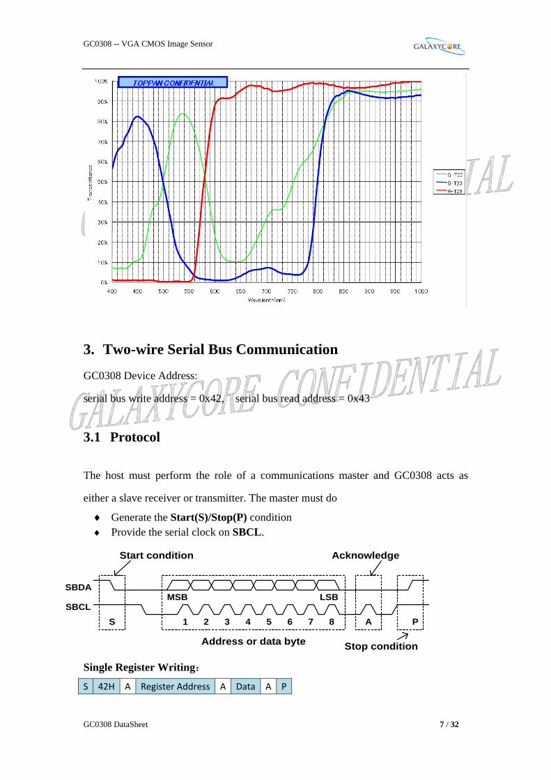
3.1 Protocol
The host must perform the role of a communications master and GC0308 acts as
either a slave receiver or transmitter. The master must do
♦ Generate the Start(S)/Stop(P) condition ♦ Provide the serial clock on SBCL.
Single Register Writing:
S 42H A Register Address A Data A P
Start condition Acknowledge
MSB LSB
1 32 4 5 6 7 8
Address or data byte
SBDA
SBCLA PS
Stop condition
GC0308 -- VGA CMOS Image Sensor
GC0308 DataSheet 8 / 32
Incremental Register Writing:
S 42H A Register Address A Data(1) A …… Data(N) A P
Single Register Reading:
S 42H A Register Address A S 43H A Data NA P
Incremental Register Reading:
S 42H A Register Address A S 43H A Data(1) A …… Data(N) NA P
Notes:
From master to slave From slave to master
S: Start condition P: Stop condition
A: Acknowledge bit NA: No acknowledge
Register Address: Sensor register address
Data: Sensor register value
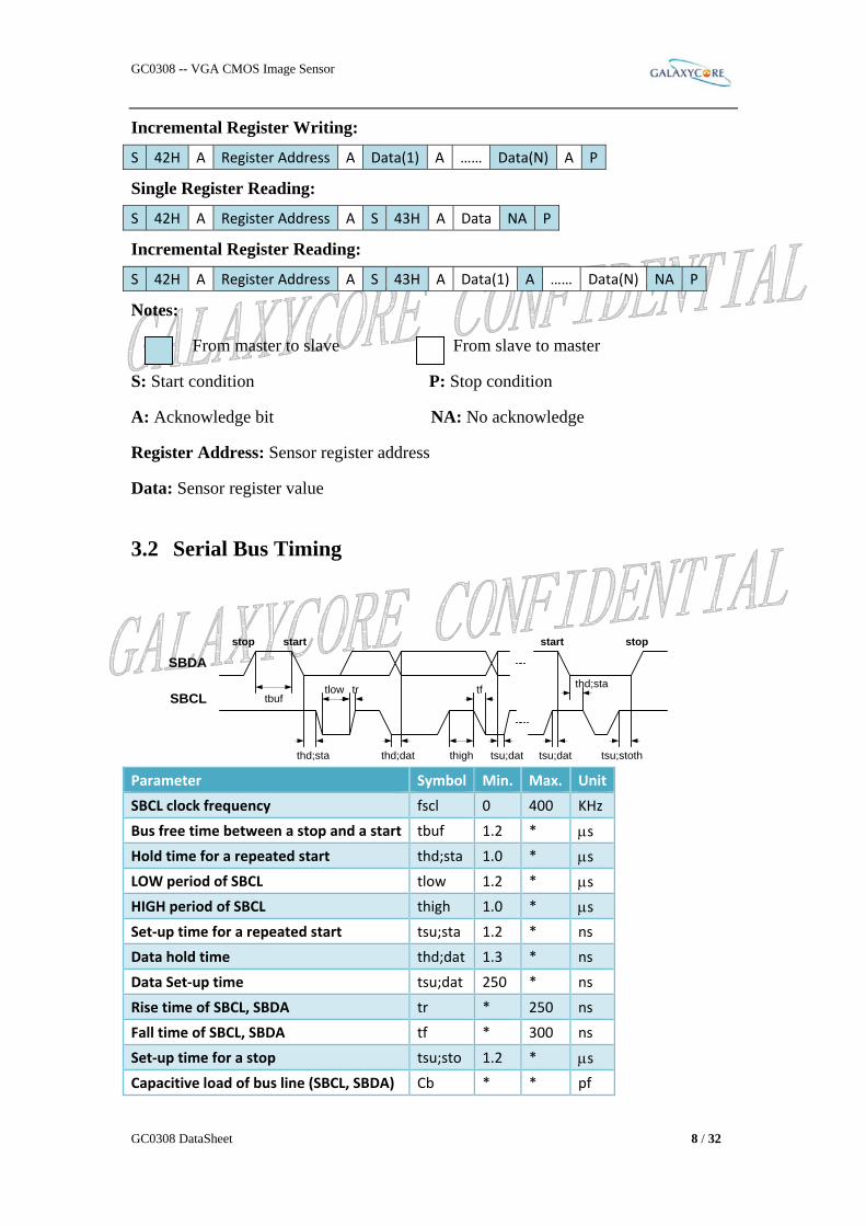
3.2 Serial Bus Timing
Parameter Symbol Min. Max. Unit
SBCL clock frequency fscl 0 400 KHz
Bus free time between a stop and a start tbuf 1.2 * µs
Hold time for a repeated start thd;sta 1.0 * µs
LOW period of SBCL tlow 1.2 * µs
HIGH period of SBCL thigh 1.0 * µs
Set‐up time for a repeated start tsu;sta 1.2 * ns
Data hold time thd;dat 1.3 * ns
Data Set‐up time tsu;dat 250 * ns
Rise time of SBCL, SBDA tr * 250 ns
Fall time of SBCL, SBDA tf * 300 ns
Set‐up time for a stop tsu;sto 1.2 * µs
Capacitive load of bus line (SBCL, SBDA) Cb * * pf
SBDA
SBCL
stop start
thigh
tftrtlow
thd;sta
tbuf
stopstart
thd;dat tsu;dat tsu;dat tsu;stoth
thd;sta

GC0308 -- VGA CMOS Image Sensor
GC0308 DataSheet 9 / 32
4. Timing
Suppose Vsync is low active and Hsync is high active, and ouput format is
YCbCr/RGB565, then the timing of vsync and hsync is bellowing:
VtSt+8 EtHSYNC
VSYNC
Ft
Bt
Ft =VB+ Vt +8 (unit is row_time)
VB = Bt + St + Et, Vblank/Dummy line,setting by register 0x0f[7:4] and 0x02.
Ft -> Frame time,one frame time
Bt -> Blank time,Vsync no active time.
St -> Start time,setting by register 0x0d.
Et –> End time,setting by register 0x0e.
Vt -> valid line time. VGA is 480,Vt=win_height-8,win_height is setting by
register 0x09 和 0x0a(488)。
When exp_time <= win_height+VB,Bt=VB-St-Et。Frame rate is controlled by
window_height+VB。
When exp_time > win_height+VB,Bt=exp_time-win_height-St-Et。Frame rate is
controlled by exp_time。
The following is row_time calculate:
row_time = Hb + Sh_delay + win_width + 4.
Hb –> HBlank or dummy pixel,Setting by register 0x0f[3:0] and 0x01.
Sh_delay -> Setting by register 0x12.
win_width -> Setting by register 0x0b and 0x0c, win_width =
6final_output_width + 8. So for VGA, we should set win_width as 648.

GC0308 -- VGA CMOS Image Sensor
GC0308 DataSheet 10 / 32
5. DC Parameters Symbol Parameter Min Typ Max Unit
VDD28 Power supply 2.7 2.8 3.3 V
IDD Active(Operating) Current ‐‐ 25 ‐‐ mA
IDDS‐PWDN Standby Current ‐‐ 10 ‐‐ uA
VIH Input voltage HIGH 0.7* VDD28 V
VIL Input voltage LOW 0.2* VDD28 V
VOH Output voltage HIGH 0.9* VDD28 V
VOL Output voltage LOW 0.1* VDD28 V
IOH Output current HIGH 8 mA
6. Register List
Analog & CISCTL
Address Name Width Default
Value
R/W Description
P0:0x00 Chip_ID 8 0x9b RO Chip version ID
P0:0x01 Hb[8:0] 8 0x6a RW Horizontal blanking, unit pixel clock
P0:0x02 Vb[8:0] 8 0x70 RW Vertical blanking, if current exposure < ( Vb +
window Height) , frame rate will be
determined by( Vb + window Height);
otherwise frame rate will be determined by
exposure time.
P0:0x03 Exposure high 4 0x0 RW [7:4] NA
[3:0] exposure[11:8],use line processing time
as the unit.
P0:0x04 Exposure low 8 0x96 Exposure[7:0], controlled by AEC if AEC is in
function
P0:0x05 Rowstart
high 1 0x00 RW Defines the starting row of the pixel array
P0:0x06 low 8 0x00
P0:0x07 Column
start
high 2 0x00 RW Defines the starting column of the pixel array
P0:0x08 low 8 0x00
P0:0x09 Window
heigh
high 1 0x1 RW Defines image height, default 488
P0:0x0a low 8 0xe8
P0:0x0b Window
width
high 2 0x2 RW Defines image width default 648
P0:0x0c low 8 0x88
P0:0x0d vs_st 8 0x02 RW [7:0] number of Row time from frame start to
first HSYNC valid
P0:0x0e vs_et 8 0x04 RW [7:0] number of Row time from last HSYNC

GC0308 -- VGA CMOS Image Sensor
GC0308 DataSheet 11 / 32
valid to frame end Notice the relation with VB,
VB > vs_st+vs_et
P0:0x0f Vb[11:8]
Hb[11:8]
4
4
0x00 RW [7:4] Vb high 4 bits
[3:0] Hb high 4 bits
P0:0x10 Rsh_width 8 0x22 RW [7:4] restg_width,X2,
[3:0] sh_width,X2,
P0:0x11 Tsp_width 8 0x0d RW [7:2] tx_width
[1:0] space width x2
P0:0x12 Sh_delay 8 0x42 RW Sample‐hold delay time after row finish
P0:0x13 Row_tail_width 4 0x00 RW [7:4] NA
[3:0] Row_tail_width, generate more hsync
for special application
P0:0x14 CISCTL_Mode1 8 0x00 RW [7] hsync_always
1: hsync always on
0: hsync output at active output
[6] NA
[5:4] CFA sequence, determined once color
filter is determined
[3:2] NA
[1] upside down
[0] mirror
P0:0x15 CISCTL_mode2 8 0x0a RW [7:6] output_mode
0 0 VGA
0 1 even skip
1 0 CIF
[5:4] reserved
[3:2] reserved
[1] new exposure mode
[0] badframe_en, don’t output bad frame
P0:0x16 CISCTL_mode3 8 0x05 RW [7:5] NA
[4] capture_ad_data_edge
1: use positive edge to sample data
0: use negative edge to sample data
[3:0] Number of A/D pipe stages
P0:0x17 CISCTL_mode4 8 0x05 RW [7:6] NA
[5:3] reserved
[2] black sun correction enable
[1:0] black sun control registers
P0:0x18 NA RW NA
P0:0x19 NA RW NA
P0:0x1a Analog mode 1 8 0x17 RW [7] rsv1, reserved register #1

GC0308 -- VGA CMOS Image Sensor
GC0308 DataSheet 12 / 32
[6] rsv0, reserved register #0
[5:4] coln_r
2’b11 100u
2’b10 80u
2’b01 60u
2’b00 40u
[3:2] comv_r
[1] clk_delay
[0] apwd, 1 will power down all analog
modules
P0:0x1b Analog mode 2 8 0x00 RW [7:2] reserved
[1:0] reserved
P0:0x1c Hrst_rsg_v18
Da_rsg
Txhigh_en
Da18_r
1
3
1
2
0x41 RW [7] hrst enable, Pixel hard reset
1: pixel hard reset enable
0: normal pixel reset
[6:4] da_rsg: row select gate low output
voltage
[3]TX_High enable
[2] NA
[1:0] da18_r, set internal D18 voltage
2’b00 1.8V
2’b01 1.88V
2’b10 1.96V
2.’b11 2.04V
P0:0x1d Vref_v25 8 0xba RW [7] vref_en, use internal reference voltage
1: use internal Vref
0: use external reference voltage supplied via
the PAD
[6:4] da_vref, set internal reference voltage
3’b000 min
3’b111 max
[3] da25_en, use internal DA25
1: use internal DA25
0: use external DA25 supplied via the PAD
[2] NA
[1:0] da25_r, set internal DA25 voltage
2’b00: 2.6V
2’b01 2.5V
2’b10 2.4V
2’b11 2.3V
P0:0x1e ADC_R 8 0x11 RW [7] reserved
[6:5] opa_r, ADC’s operating current
GC0308 -- VGA CMOS Image Sensor
GC0308 DataSheet 13 / 32
[4:2] NA
[1:0] sref
P0:0x1f PAD_drv 8 0x15 RW [7:6] NA
[5:4]sync_drv
0 0: 4mA,
01: 8mA,
10: 12mA,
11: 16mA
[3:2]data_drv
0 0: 4mA,
01: 6mA,
10: 10mA,
11: 12mA
[1:0] pclk_drv
0 0: 2mA,
01: 4mA,
10: 8mA,
11: 10mA
P0:0xfe Rest related 8 RW [7] soft_reset
[6:5] NA
[4] CISCTL_restart_n, restart CISCTL, effective
low
[3:1]NA
[0] page_select
1’b0 frequently used registers in REGF0
1’b1 registers in REGF1

GC0308 -- VGA CMOS Image Sensor
GC0308 DataSheet 14 / 32
ISP Related
Address Name Width Default
Value
R/W Description
P0:0x20 Block_enable_1 8 0xff RW [7] BKS_en
[6] gamma enable
[5] CC enable
[4] Edge enhancement enable
[3] Interpolation enable
[2] Noise removal enable
[1] Defect removal enable
[0] Lens‐shading correction enable
P0:0x21 Block_enable_2 8 0xff RW [7] NA
[6] blue_edge_en
[5] skin correction enable
[4] CbCr_HUE_en
[3] Y_as_en
[2] autogray_en
[1] Y_gamma_en
[0] HSP_en
P0:0x22 AAAA_enable 8 0x40 RW [7] NA
[6] auto_DNDD_en
[5] auto_EE
[4] auto_SA
[3] NA
[2] ABS enable
[1] AWB enable
[0] NA
P0:0x23 special_effect 8 0x00 RW [7:3] NA
[2] edge_map
[1] CbCr fixed enable
[0] Inverse color
P0:0x24 Output_format 8 0xa2 RW [7] ISP high 8 or low 8
[6] output_delay_or_not
[5] average chroma
[4:0]output data mode
5’h00 Cb Y Cr Y
5’h01 Cr Y Cb Y
5’h02 Y Cb Y Cr
5’h03 Y Cr Y Cb
5’h06 RGB 565
5’h07 RGB x555

GC0308 -- VGA CMOS Image Sensor
GC0308 DataSheet 15 / 32
5’h08 RGB 555x
5’h09 RGB x444
5’h0a RGB 444x
5’h0b BGRG
5’h0c RGBG
5’h0d GBGR
5’h0e GRGB
5’h0f bypass 10bits
5’h11 only Y
5’h12 only Cb
5’h13 only Cr
5’h14 only R
5’h15 only G
5’h16 only B
5’h17 switch odd/even column /row to
controls output bayer pattern
P1:0x53[6:5]:
0 0 RGBG
0 1 RGGB
10 BGGR
11 GBRG
5’h18 DNDD_out_mode, high 8
5’h19 LSC_out_mode, high 8
P0:0x25 output_en 4 0x00 RW [3]data_en,
[2]pclk en
[1]hsync_en,
[0]vsync_en
P0:0x26 sync_mode 8 0x3f RW Synchronize signal output mode
[7] data delay half
[6] hsync delay half
[5] allow pclk around hsync
[4] allow pclk around vsync
[3] opclk gated in HB
0: not gated
1: gated
[2] opclk polarity
0: invert of isp_2pclk(isp_pclk)
1: same as isp_2pclk(isp_pclk)
[1] hsync polarity
0: low valid
1: high valid
[0] vsync polarity

GC0308 -- VGA CMOS Image Sensor
GC0308 DataSheet 16 / 32
0: low valid
1: high valid
P0:0x27 NA
P0:0x28 clk_div_mode 3 0x00 RW [6:4] +1 represent the frequency division
number
[2:0] represent the high level in one pulse
after frequency division
Mclk by Div duty
0x11 2 1:1
0x21 3 1:2
0x22 3 2:1
0x31 4 1:3
0x32 4 2:2
0x33 4 3:1
…
0x76 8 6:2
0x77 8 7:1
P0:0x29 bypass_mode 8 0x83 RW [7]allow_hsync_in_row_tail
[6]single_2_double_mode
[5]first_second_switch
[4]isp_bypass_no_gate_mode
[3]is_8bit_bypass
[2]is_10bit_bypass
[1:0]bypass which 8bits from 11bit, in
is_8bit_bypass mode
11: [10:3]
10: [9:2]
01: [8:1]
00: [7:0]
P0:0x2a Clock_gating_en 8 0xff RW [7] ISP quiet mode
[6:0] reserved
P0:0x2b dither_mode 8 0x00 RW [2]dither_en
[1:0]dither to which stage
P0:0x2c dither_bit 8 0x00 RW Dither_bit
P0:0x2d
Debug_mode1
8
0x08
RW
[7:4] NA
[3:2] pipe gate mode
[1] AWB_gain_mode
[0] more boundary mode
P0:0x2e Debug_mode2 8 0x00 RW [7:6] NA
[5] reserved
[4] NA
[3] skin_map

GC0308 -- VGA CMOS Image Sensor
GC0308 DataSheet 17 / 32
[2]NA
[1] test image type1
[0] test image type2
P0:0x2f Debug_mode3 8 0x01 RW [7:1]NA
[0] update_gain_mode
P0:0x46 Crop_win_mode
Crop _win_y1
Crop_win_x1
8 0x0
0x0
0x0
RW [7] crop window mode enable
[6] NA
[5:4] Crop win y0[9:8]
[2:0] Crop win x0[10:8]
P0:0x47 Crop _win_y1 8 0x00 RW Crop _win_y0[7:0]
P0:0x48 Crop _win_x1 8 0x00 RW Crop _win_x0[7:0]
P0:0x49 Crop_win_height 1 0x01 RW [7:1] NA
[0] Crop _win_height[8]
P0:0x4a Crop_win_height 8 0xe0 RW Crop _win_height[7:0]
P0:0x4b Crop_win_width 2 0x02 RW [7:2] NA
[1:0] Crop _win_width[9:8]
P0:0x4c Crop_win_width 8 0x80 RW Crop _win_width[7:0]
BLK
Address Name Width Default
Value
R/W Description
P0:0x30 Blk_mode 8 0x24 RW [7] dark current mode
[6:4] BLK smooth speed
[3:2] BLK Row select mode
[1] dark current measure enable
[0] offset enable
P0:0x31 Blk_limit_value 7 0x40 RW [7] NA
[6:0] Blk value limit
P0:0x32 Global_offset 7 0x01 RW [7] NA
[6:0] X2, global offset value
P0:0x33 Current_R_offset 6 RO [7] NA
[6:0] Current_R_offset
P0:0x34 Current_G_offse
t
6 RO [7] NA
[6:0] Current_G_offset
P0:0x35 Current_B_offset 6 RO [7] NA
[6:0] Current_B_offset
P0:0x36 Current_R_dark_
current
6 RO [7] NA
[6:0] Current_R_dark_current
P0:0x37 Current_G_dark
_current
7 RO [7] NA
[6:0] Current_G_dark_current
P0:0x38 Current_B_dark_ 8 RO [7] NA

GC0308 -- VGA CMOS Image Sensor
GC0308 DataSheet 18 / 32
current [6:0] Current_B_dark_current
P0:0x39 Exp_rate_darkc 8 0x04 RW Exp_rate_darkc
P0:0x3a offset_submode,
offset_ratio
2
6
0x00
0x20
RW [7:6] offset sub mode
[5:0] offset ratio, 1.5 bits
P0:0x3b darkc_submode,
dark_current_rat
io
2
6
0x00
0x10
RW [7:6] dark current sub mode
[5:0] dark current ratio, 1.5 bits
P0:0x3c Manual_G1_offs
et
6 0x02 RW
S5
P0:0x3d Manual_R1_offs
et
6 0x3e RW
S5
P0:0x3e Manual_B2_offs
et
6 0x3f RW
S5
P0:0x3f Manual_G2_offs
et
6 0x03 RW
S5
PREGAIN
Address Name Width Default
Value
R/W Description
P0:0x50 Global_gain 6 0x12 RW [7:6] NA
[5:0] global_gain, 2.4bits, 0x10 is 1.0x
P0:0x51 Auto_pregain 8 0x40 RO Controlled by AEC , can be manually
controlled when disable AEC
P0:0x52 Auto_postgain 8 0x40 RO Controlled by AEC , can be manually
controlled when disable AEC
P0:0x53 Channel_gain_G
1
8 0x80 RW 1.7 bits, G1 channel pre gain
P0:0x54 Channel_gain_R 8 0x80 RW 1.7 bits, R channel pre gain
P0:0x55 Channel_gain_B 8 0x80 RW 1.7 bits, B channel pre gain
P0:0x56 Channel_gain_G
2
8 0x80 RW 1.7 bits, G2 channel pre gain
P0:0x57 R_ratio 8 0x80 RW 1.7 bits, R_ratio
P0:0x58 G_ratio 8 0x80 RW 1.7 bits, G_ratio
P0:0x59 B_ratio 8 0x80 RW 1.7 bits, B_ratio
P0:0x5a AWB_R_gain 8 0x50 RW 2.6 bits, red channel gain from AWB
P0:0x5b AWB_G_gain 8 0x40 RW 2.6 bits, green channel gain from AWB
P0:0x5c AWB_B_gain 8 0x48 RW 2.6 bits, blue channel gain from AWB
P0:0x5d Lsc_decrease_le
vel1
6 0x12 RW [7:6] NA
[5:0] 4.2bits, Lsc_decrease_level1_gain
P0:0x5e Lsc_decrease_le
vel2
6 0x1a RW [7:6] NA
[5:0] 4.2bits, Lsc_decrease_level2_gain

GC0308 -- VGA CMOS Image Sensor
GC0308 DataSheet 19 / 32
P0:0x5f Lsc_decrease_le
vel3
6 0x24 RW [7:6] NA
[5:0] 4.2bits, Lsc_decrease_level3_gain
LSC
Address Name Width Default
Value
R/W Description
P0:0x8b LSC red b2 8 0x40 RW Square coefficient for R,G,B channel
P0:0x8c LSC green b2 8 0x40 RW
P0:0x8d LSC blue b2 8 0x40 RW
P0:0x8e LSC red b4 8 0x30 RW Quadra coefficient for R,G,B channel
P0:0x8f LSC green b4 8 0x30 RW
P0:0x90 LSC blue b4 8 0x30 RW
P0:0x91 Signed b4
LSC row center
1
7
0x60
RW
[7] controls the sign of quadric coefficient,
default 0
[6:0] row center for LSC correction X4
P0:0x92 LSC column
center
8 0x80 RW
Column center for LSC correction X4
ASDE (auto saturation de-noise and edge enhancement)
Address Name Wid
th
Default
Value
R/W Description
P0:0x69 ASDE gain high
threshold
8 0x20 RW Gain high threshold, 4.4bits,
P0:0x6a ASDE_DN_c_slope
,ASDE_gain_mode
4
4
0x0a
0x0f
RW [7:4] de noise center slope, float 1.3
[3] select current post gain,
[2] selects current pre gain
[1] select global gain
[0] NA
P0:0x6b ASDE_DN_b_slope
ASDE_DN_n_slope
4
4
0x0a
0x0a
RW [7:4] ASDE_DN_b_slope
[3:0] ASDE_DN_n_slope
P0:0x6c ASDE_DD_bright
_th_start
ASDE_DD_brigth
_th_slope
4
4
0x05
0x0f
RW [7:4] ASDE_DD_bright _th_start
[3:0] ASDE_DD_brigth _th_slope
P0:0x6d ASDE_DD_limit
_start
ASDE_DD_limit
_slope
4
4
0x08
0x0f
RW [7:4] ASDE_DD_limit _start
[3:0] ASDE_DD_limit _slope
P0:0x6e ASDE_auto_EE1
_effect_start
4
0x05
RW [7:4] ASDE_auto_EE1 _effect_start
[3:0] ASDE_auto_EE1 _effect_slope

GC0308 -- VGA CMOS Image Sensor
GC0308 DataSheet 20 / 32
ASDE_auto_EE1
_effect_slope
4 0x08
P0:0x6f ASDE_auto_EE2
_effect_start
ASDE_auto_EE2
_effect_slope
4
4
0x04
0x08
RW [7:4] ASDE_auto_EE2 _effect_start,
[3:0] ASDE_auto_EE2 _effect_slope,
P0:0x70 ASDE_auto_
saturation_dec_sl
ope
8 0x10 RW ASDE_auto_ saturation_dec_slope
P0:0x71 ASDE_auto_
saturation_low_li
mit
ASDE_sub
_saturation_slope
4
4
0x03
0x01
RW [7:4] ASDE_auto_ saturation_low_limit,
[3:0] ASDE_sub _saturation_slope
DNDD
Address Name Width Default
Value
R/W Description
P0:0x60 DN_mode_en 8 0x07 RW [7:5] NA
[4] zero_weight_mode
[3] share mode
[2] c_weight_adap_mode
[1] dn_lsc_mode
[0] dn_b_mode
P0:0x61 DN_mode_ratio 0x22 RW [7:6] NA
[5:4] C_weight_adaptive_ratio
[3:2] dn_lsc_ratio
[1:0] dn_b_mode_ratio
P0:0x62 DN_bilat_b_base 6 0xc RW Fixed bilateral b value
P0:0x63 DN_b_incr 5 0x0 RW [7:5] NA
[4:0] increase de‐noise at low luminance
condition, controlled by ASDE module
P0:0x64 DN_bilat_n_base
DN_C_weight
4
4
0x00
0x05
RW [7:4] Base noise level of each frame
[3:0] base center pixel weight
P0:0x65 DN_n_incr
DN_C_coeff
4
4
0x08
0x08
RW [7:4] DN_n_incr
[3:0] DN_C_coeff
controlled by ASDE module or user
P0:0x66 DD_dark_bright_
TH
4 0xe RW [7:4] dark threshold
[3:0] bright threshold controlled by ASDE or
user, should be set >=2
P0:0x67 DD_flat_TH 8 0x86 RW Threshold to define a flat

GC0308 -- VGA CMOS Image Sensor
GC0308 DataSheet 21 / 32
P0:0x68 DD_limit
DD_ratio
4
4
0x08
0x02
RW [7:4] DD_limit, threshold of a defect pixel
[3:2] NA
[1:0] DD_ratio, controls the difference
between bright and dark pixel
INTPEE (Interpolation and Edge Enhancement) Address Name Width Default
Value
R/W Description
P0:0x72 EEINTP mode 1 8 0xec RW [7] edge add mode1
[6] new edge mode (HP3 mode )
[5] edge2 mode
[4] HP mode
[3] LP interpolation enable
[2] LP edge enable
[1:0] LP edge mode
P0:0x73 EEINTP mode 2 8 0x80 RW [7] edge_add_mode2
[6]NA
[5] direction mode
[4] fixed direction threshold
[3:0] reserved
P0:0x74 Direction TH1 6 0x05 RW Lower Criteria for direction detection
P0:0x75 Direction TH2 6 0x3f RW Upper Criteria for direction detection
P0:0x76 Diff_HV_TI_TH
Direction diff TH
4
4
0x05
0x00
RW [7:4] Diff_HV_TI_TH
[3:0] Direction diff TH
P0:0x77 Edge1 effect
Edge2 effect
4
4
0x08
0x04
RW [7:4] edge effect1
[3:0] edge effect 2
Controlled by user or ASDE
P0:0x78 Edge_pos_ratio
Edge_neg_ratio
4
4
0x08
0x08
RW [7:4] pos edge ratio , 1.3Bits
[3:0] neg edge ratio , 1.3Bits
P0:0x79 Edge1_max
Edge1_min
4
4
0x6
0x1
RW [7:4] edge1 max
[3:0] edge1 min
P0:0x7a Edge2_max
Edge2_min
4
4
0x6
0x1
RW [7:4] edge2 max
[3:0] edge2 min
P0:0x7b Edge1_th
Edge2_th
4
4
0x2
0x2
RW [7:4] edge1 threshold
[3:0] edge2 threshold
P0:0x7c Edge_pos_max
Edge_neg_max
4
4
0x0f
0x08
RW [7:4] Pos_edge_max
[3:0] Neg_edge_max
ABB
Address Name Width Default
Value
R/W Description

GC0308 -- VGA CMOS Image Sensor
GC0308 DataSheet 22 / 32
P0:0x80 ABB mode 3 0x03
RW
[7:3] NA
[2:1] ABB row select mode
[0] ABB enable
P0:0x81 ABB target
average
8 0x05 RW
S7,black stretch target average, allow
negative target value.
P0:0x82 ABB target
average
8 0x33 RW
S7, black stretch target average, allow
negative target value
P0:0x83 ABB limit value 7 0x20 RW
[7] NA
[6:0] black point criteria
P0:0x84 ABB speed 8 0x22
RW
[7] NA
[6:4] fast speed
[3] NA
[2:0] IIR smooth speed
P0:0x85 Current R black
level
7 0x08
RW
[7] NA
[6:0] channel R black level aligns to lower 7
bit of 10 bit input data, controlled by ABB
or user
P0:0x86 Current G black
level
7 0x09
RW
[7] NA
[6:0] channel G black level aligns to lower 7
bit of 10 bit input data, controlled by ABB
or user
P0:0x87 Current B black
level
7 0x0a
RW
[7] NA
[6:0] channel B black level aligns to lower 7
bit of 10 bit input data, controlled by ABB
or user
P0:0x88 Current R black
factor
8 0x09 RW
Used to fine tune R black value,Lower 8 of
10,controlled by ABB or user
P0:0x89 Current G black
factor
8 0x0b RW
Used to fine tune G black value,Lower 8 of
10,controlled by ABB or user
P0:0x8a Current B black
factor
8 0x0d RW
Used to fine tune B black value,Lower 8 of
10,controlled by ABB or user
CC
Address Name Width Default
Value
R/W Description
P0:0x93 CC Matrix C11 8 0x44 RW R channel coefficient 1, S1.6
P0:0x94 CC Matrix C12 8 0xfe RW R channel coefficient 2, S1.6
P0:0x95 CC Matrix C13 8 0xfe RW R channel coefficient 3, S1.6
P0:0x96 CC Matrix C21 8 0xfe RW G channel coefficient 1, S1.6
P0:0x97 CC Matrix C22 8 0x44 RW G channel coefficient 2, S1.6

GC0308 -- VGA CMOS Image Sensor
GC0308 DataSheet 23 / 32
P0:0x98 CC Matrix C23 8 0xfe RW G channel coefficient 3, S1.6
P0:0x9c CC Matrix C41 5 0x00 RW R channel offset coefficient, S4
P0:0x9d CC Matrix C42 5 0x00 RW G channel offset coefficient, S4
P0:0x9e CC Matrix C43 5 0x00 RW B channel offset coefficient, S4
GAMMA
Address Name Width Default
Value
R/W Description
P0:0x9f Gamma_out0 8 0x10 RO Each out value of knee_i. Knee0=0
P0:0xa0 Gamma_out1 8 0x20 RO Knee1=8
P0:0xa1 Gamma_out2 8 0x38 RO Knee2=16
P0:0xa2 Gamma_out3 8 0x4E RO Knee3=24
P0:0xa3 Gamma_out4 8 0x63 RO Knee4=32
P0:0xa4 Gamma_out5 8 0x76 RO Knee5=40
P0:0xa5 Gamma_out6 8 0x87 RO Knee6=48
P0:0xa6 Gamma_out7 8 0xa2 RO Knee7=64
P0:0xa7 Gamma_out8 8 0xb8 RO Knee8=80
P0:0xa8 Gamma_out9 8 0xca RO Knee9=96
P0:0xa9 Gamma_out10 8 0xd8 RO Knee10=112
P0:0xaa Gamma_out11 8 0xe3 RO Knee11=128
P0:0xab Gamma_out12 8 0xe9b RO Knee12=144
P0:0xac Gamma_out13 8 0xf0 RO Knee13 =160
P0:0xad Gamma_out14 8 0xf8 RO Knee14 = 192
P0:0xae Gamma_out15 8 0xfd RO Knee15 = 224
P0:0xaf Gamma_out16 8 0xff RO Knee16 = 256
YCP
Address Name Width Default
Value
R/W Description
P0:0xb0 Global saturation 8 0x40 RW Global saturation, controlled by auto_
saturation
P0:0xb1 saturation_Cb 8 0x30 RW
Cb saturation
3.5bits, 0x20=1.0
P0:0xb2 saturation_Cr 8 0x30 RW
Cr saturation
3.5bits, 0x20=1.0
P0:0xb3
luma_contrast 8 0x40 RW
Luma_contrast, can be adjusted via
contrast center
2.6bits, 0x40=1.0
P0:0xb4 Contrast center 8 0x80 RW Contrast center value
P0:0xb5 Luma_offset 8 0x00 RW Add offset on luma value. S7.
GC0308 -- VGA CMOS Image Sensor
GC0308 DataSheet 24 / 32
P0:0xb6 skin_Cb_center 8 0xe8 RW Cb criteria for skin detection.
P0:0xb7 skin_Cr_center 4 0x18 RW Cr criteria for skin detection.
P0:0xb8 Skin radius
square 8 0x28 RW
Defines skin range
P0:0xb9 Skin brightness
high
Skin brightness
low
4
4
0xe
0x3
RW [7:4] skin brightness high threshold
[3:0] skin brightness low threshold
P0:0xba
Fixed_Cb 8 0x00 RW
S7, if fixed CbCr function is enabled, current
image Cb value will be replace by this value
to achieve special effect
P0:0xbb
Fixed_Cr 8 0x00 RW
S7, if fixed CbCr function is enabled, current
image Cr value will be replace by this value
to achieve special effect
P0:0xbc NA
P0:0xbd Edge_dec_sa_en
Edge_dec_sa_slo
pe
3
4 RW
[7] NA
[6:4] edge_dec_sa_en
[3:0] edge_dec_sa_slope
P0:0xbe auto‐gray mode
Sa_autogray
2
4
0x12 [7:6] NA
[5:4] auto gray mode
[3:0] sa_autogray point
P0:0xbf Saturation_sub_
strength
8 0x00 RO Chroma offset in low light
P0:0xc0 Y_Gamma_out0 8 RW Knee0=0
P0:0xc1 Y_Gamma_out1 8 RW Knee1=8
P0:0xc2 Y_Gamma_out2 8 RW Knee2=16
P0:0xc3 Y_Gamma_out3 8 RW Knee3=32
P0:0xc4 Y_Gamma_out4 8 RW Knee4=48
P0:0xc5 Y_Gamma_out5 8 RW Knee5=64
P0:0xc6 Y_Gamma_out6 8 RW Knee6=80
P0:0xc7 Y_Gamma_out7 8 RW Knee7=96
P0:0xc8 Y_Gamma_out8 8 RW Knee8=128
P0:0xc9 Y_Gamma_out9 8 RW Knee9=160
P0:0xca Y_Gamma_out1
0
8 Knee10=192
P0:0xcb Y_Gamma_out1
1
8 Knee11=224
P0:0xcc Y_Gamma_out1
2
8 Knee12=255
GC0308 -- VGA CMOS Image Sensor
GC0308 DataSheet 25 / 32
AEC
Address Name Width Default
Value
R/WDescription
P0:0xd0 AEC_mode1 8 0xca RW [7] reserved
[6] NA
[5] exposure mode
1: level exp
0: N step mode
[4] NA
[3: 2] gain mode
[1] measure point
[0] skip mode in luminance detection
P0:0xd1 AEC_mode2 8 0x21 RW [7] fix target
[6:4] AEC take action every N frame
[3:2] close frame number to eliminate bad
frame
[1] change exp_gain_mode
[0] dead_zone_mode
P0:0xd2 AEC_mode3 8 0x00 RW [7] AEC_en
[6] map measure point
[5] color Y mode
[4] skin weight mode
[3] NA
[2] color select
[1:0] NA
P0:0xd3 AEC_target_Y 8 0x48 RW expected luminance value
P0:0xd4 Y_average 8 0x00 RO Current frame luma average
P0:0xd5 AEC_high_low
_range
8 0xf2 RW [7:4] x16, count limit for high luminance
pixels
[3:0] x4, count limit for low luminance
pixels
P0:0xd6 AEC_ignore 5 0x18 RW [4] aec_ignore_enable
[3:0] aec ignore number
P0:0xd7 AEC_number_li
mit_high_range
8 0x35 AEC_number_limit_high_range
P0:0xd8 NA
P0:0xd9 AEC_skin_offset
AEC_R_offset
4
4
0x88 RW [7:4] AEC_skin_offset
[3:0] AEC_R_offset
P0:0xda AEC_G_offset
AEC_B_offset
4
4
0x88 RW [7:4] AEC_G_offset
[3:0] AEC_B_offset
P0:0xdb AEC_slow_margi 4 0x9 RW [7:4] AEC slow margin, X4

GC0308 -- VGA CMOS Image Sensor
GC0308 DataSheet 26 / 32
n
AEC_slow_speed
3 0x6 [3] NA
[2:0] AEC slow speed
P0:0xdc AEC_fast_margin
AEC_fast_speed
4
3
0x9
0x6
RW [7:4] AEC fast margin, X4
[3] NA
[2:0] AEC fast speed
P0:0xdd AEC_exp_change
_gain_ratio
8 0x96 RW Gain change criteria, float 1.7, default use
1.2x
P0:0xde AEC_step2_sunli
ght 8 0x02 RW AEC_step2_sunlight
P0:0xdf AEC_I_frames
AEC_D_ratio
2
4
0x33 RW [7:6] NA
[5:4] integration period
[3:0] differential coefficient
P0:0xe0 AEC_I_stop_L
_margin
7 0x7 RW [7] NA
[6:0] x2, AEC_I_stop_L _margin
P0:0xe1 AEC_I_stop_mar
gin
AEC_I_ratio
4
4
0x61 RW [7:4] AEC adjust stop margin
[3:0] integration coefficient
P0:0xe2 Anti_flicker_step
[11:8]
4 0x0 RW [7:4] NA
[3:0] flicker step [11:8]
P0:0xe3 Anti_flicker_step
[7:0]
8 0x96 RW [7:0] flicker step [7:0]
P0:0xe4 exp level_1 high 4 0x02 RW Exposure level 1
P0:0xe5 exp level_1 low 8 0x58 RW
P0:0xe6 exp level_2 high 4 0x03 RW Exposure level 2
P0:0xe7 exp level_2 low 8 0x84 RW
P0:0xe8 exp_level_3 high 4 0x07 RW Exposure level 3
P0:0xe9 exp_level_3 low 8 0x08 RW
P0:0xea exp_level_4 high 4 0x0d RW Exposure level 4
P0:0xeb exp_level_4 low 8 0x7a RW
P0:0xec
Max_exp_level
Exp_min_l[11:8]
2
4 0x20 RW
[7:6] NA
[5:4] max exposure levels can be applied by
AEC
[3:0] minimum exposure level high 4 bits
P0:0xed Exp_min_l[7:0] 8 0x4 RW minimum exposure level lower 8 bits
P0:0xee Max_post_dg_ga
in 8 0xc0 RW
Digital post gain limit, float 2.6 ,X3
P0:0xef Max_pre_dg_gai
n 8 0x60 RW
Digital pre gain limit, float 2.6, X1.5

GC0308 -- VGA CMOS Image Sensor
GC0308 DataSheet 27 / 32
ABS
Address Name Width Default
Value
R/W Description
P0:0xf0 ABS_range_com
pesate
ABS_skip_frame
4
3
0x3 RW [7:4] X4+3, add "more range" to enlarge
more stretch
[3] NA
[2:0] Set number of frames to be skipped in
ABS adjustment
P0:0xf1 ABS_stop_margi
n
4 0x2 RW [7:4] NA
[3:0] margin for ABS to stop adjustment
P0:0xf2 Y_S_compesate
ABS_manual_K
4
4
0x00 RW [7:4] Y_S_compesate
[3:0] manual ABS slope adjustment, default
0
P0:0xf3 Y_stretch_limit 7 0x30 RW [7] NA
[6:0] Y_stretch limit
P0:0xf4 Y_tilt 8 RO [7:0] the corner point, stretch Y if less than
it
P0:0xf5 Y_stretch_K 8 RO [7:0] the slope ABS calculated for Y less
than Y_tilt, 2.6bits
Measure Window
Address Name Width Default
Value
R/W Description
P0:0xf7 Big_win_x0 6 0x04 RW
Measure big window left column number,
X4
P0:0xf8 Big_win_y0 6 0x02 RW Measure big window left row number, X4
P0:0xf9 Big_win_x1 8 0x98 RW
Measure big window right column number,
X4
P0:0xfa Big_win_y1 8 0x70 RW Measure big window right row number, X4
P0:0xfb Diff_Y_big_thd 0x20 RW Light change threshold
OUT Module
Address Name Width Default
Value
R/W Description
P1:0x50 Close_frame_en
Close_frame_nu
m
1
4
0x00 RW [7:5] NA
[4] close frame function enable, close
output Vsync to control frame rate
[3:0] frames to be closed should be
selected from this pool
P1:0x51 Close_frame_nu 8 0x00 RW These two registers is a combi of four 4bit

GC0308 -- VGA CMOS Image Sensor
GC0308 DataSheet 28 / 32
m1 registers, they defines up to any 4 frames
to be closed P1:0x52 Close_frame_nu
m2
8 0x00 RW
P1:0x53 Bayer_mode 8 0x82 RW [7] opclk gated enable in subsample
[6] odd even row switch
[5] odd even column switch
[4:0] pixel count limit to extend row in tail,
do NOT less than 2
P1:0x54 subsample
8 0x03 RW
[7] use_or_cut_row
[6:4]subsample row ratio
[3] use_or_cut_col
[2:0]subsample col ratio
P1:0x55 sub_mode
2 0x03 RW[1] neighbor vag mode
[0] subsample_extend_opclk
P1:0x56 sub_row_N1 6 0x00 RW
[5:3]sub_row_num1
[2:0] sub_row_num2
P1:0x57 sub_row_N2 6 0x00 RW
[5:3]sub_row_num3
[2:0] sub_row_num4
P1:0x58 sub_col_N1 6 0x00 RW
[5:3]sub_col_num1
[2:0] sub_col_num2
P1:0x59 sub_col_N2 6 0x00 RW
[5:3]sub_col_num3
[2:0] sub_col_num4
AWB
Address Name Width Default
Value
R/W Description
P1:0x00 AWB_RGB
_high_low
8 0xf5 RW Defines the RGB range of gray pixel to be
selected
P1:0x02 AWB_Y_to_C_dif
f2
8 0x18 RW Gray pixel criteria
P1:0x04 AWB_C_max 8 0x02 RW Chroma limit
P1:0x05 AWB_C_inter 8 0x22 RW Slope of interested zone upper bond
P1:0x06 AWB_C_inter2 8 0x40 RW Slope of interested zone lower bond
P1:0x08 AWB_C_max_big 8 0x50 RW Chroma limit when big_c mode enable
P1:0x09 AWB_Y_high 8 0x40 RW Give high luminance point more weight
P1:0x0a AWB_number_li
mit
8 0x90 RW Number limit

GC0308 -- VGA CMOS Image Sensor
GC0308 DataSheet 29 / 32
P1:0x0b Kwin_ratio
Sel_point
Skip_mode
3
1
2
0x6
0
0
RW [7] NA
[6] block threshold selection
1: use maximum threshold
0: use threshold defined by [5:4],
default
[5:4] small blocks validation criteria
[3] NA
[2] AWB sample location
[1:0]AWB skip mode
P1:0x0c Kwin_thd 3 0x6 RW [7:5] NA
[4:0] block min range limit
P1:0x0d Light_gain_range 8 0x30 RW Defines gain_range in R/B_gain domain.
P1:0x0e Small_win
_width_step
8 0x49 RW Small_win _width_step
P1:0x0f Small_win
_height_step
8 0x36 RW Small_win _height_step
P1:0x10 AWB_yellow_TH
AWB_big_c_limit
4
4
0x42 RW [7:4] AWB yellow block threshold
[3:0] AWB_big_c_block_limit
P1:0x11 AWB_mode 8 0xf RW reserved
P1:0x12 AWB_adjust_spe
ed
AWB_adjust_ma
rgin
3
4
0x42 RW [7] NA
[6:4] AWB gain adjust speed, the bigger the
quicker.
[3:0] AWB_adjust_margin
P1:0x13 AWB_every_N
AWB_light
ct_mode
2
4
0x21 RW [7:6] NA
[5:4] AWB every N
[3] No FIR
[2] FIR smooth mode
[1] NA
[0] use ct mode
P1:0x14~
0x1e
AWB_set1 8 ‐‐ RW reserved
P1:0x70~
0x79
AWB_set2 8 ‐‐ RW reserved
P1:0xd0 R_avg_use 8 RO R_avg_use
P1:0xd1 G_avg_use 8 RO G_avg_use
P1:0xd2 B_avg_use 8 RO B_avg_use

GC0308 -- VGA CMOS Image Sensor
GC0308 DataSheet 30 / 32
A
B
C
D
Array Center(-129.273,169.516)
Chip Center(0,0)
7. Pin Description
7.1 GC0308 CSP package Top view(unit:um)
1 2 3 4 5
7.2 CSP ball description
7.3 GC0308 chip pin description
Pin Name Pin Type Function
A1 AVDD25 Power Internal analog voltage. Please connect
0.1uF or 0.47uF capacity to ground.
A2 VREF Power Internal reference voltage. Please connect
0.1uF or 0.47uF capacity to ground.
A3 SBDA I/O Two‐wire serial bus, data
A4 SBCL Input Two‐wire serial bus, clock
1 2 3 4 5
A AVDD25 VREF SBDA SBCL D<7>
B GND PWDN HSYNC D<6> D<5>
C VSYNC D<0> D<3> D<4> PCLK
D DVDD28 D<1> D<2> RESETB INCLK

GC0308 -- VGA CMOS Image Sensor
GC0308 DataSheet 31 / 32
A5 D<7> Output YUV/RGB data output bit[7]
B1 GND Ground Chip ground
B2 PWDN Input Sensor power down control:
0:normal work
1:standby
B3 HSYNC Output HSYNC output
B4 D<6> Output YUV/RGB data output bit[6]
B5 D<5> Output YUV/RGB data output bit[5]
C1 VSYNC Output VSYNC output
C2 D<0> Output YUV/RGB data output bit[0]
C3 D<3> Output YUV/RGB data output bit[3]
C4 D<4> Output YUV/RGB data output bit[4]
C5 PCLK Output Pixel clock output
D1 DVDD28 Power Main power supply pin, typical 2.8V,
Please connect 0.1uF or 0.47uF capacity to
ground.
D2 D<1> Output YUV/RGB data output bit[1]
D3 D<2> Output YUV/RGB data output bit[2]
D4 RESETB Input Chip reset control:
0:chip reset
1:normal work
D5 INCLK Input Main clock

GC0308 -- VGA CMOS Image Sensor
GC0308 DataSheet 32 / 32
7.4 CSP package mechanical drawing (unit:um)
Description Symbol Nominal Min. Max.
Millimeters
Package Body Dimension X A 3.290 3.265 3.315
Package Body Dimension Y B 2.758 2.733 2.783
Package Height C 0.775 0.715 0.835
Ball Height C1 0.160 0.130 0.190
Package Body Thickness C2 0.615 0.580 0.650
Thickness from top glass surface to wafer C3 0.435 0.415 0.455
Ball Diameter D 0.300 0.270 0.330
Total Ball Count N 20
Ball Count X axis N1 5
Ball Count Y axis N2 4
Pins Pitch X axis J1 0.600
Pins Pitch Y axis J2 0.600
Edge to Pin Center Distance along X S1 0.445 0.415 0.475
Edge to Pin Center Distance along Y S2 0.479 0.449 0.509
Recommended