TW2809C
Multichannel H.264 Audio/Video Codec
FN7875 Rev. 1.00 Page 1 of 130
February 27, 2014
FN7875
Rev. 1.00
February 27, 2014
DATASHEET
Features
TW2809C is a high performance and cost
effective multi-channel H.264 codec solution
designed for security surveillance market. It is
capable of encoding and decoding maximum 8
channels standard definition (SD) video in real
time. It can do high definition (HD) 1080x60i
encode or decode at real time too. Each video
channel can be independently controlled in terms
of encode / decode mode, frame rate, bit rate,
and resolution. TW2809C is an ideal H.264 codec
candidate for different DVR platforms such as
16CH SD or 16CH CIF.
Video Features
Real time full-duplex video codec compliant to
H.264 main profile standard
Supports real time full duplex 9 channel SD
encode and/or decode
Supports CIF JPEG or H.264 network stream
encode
Supports CBR and VBR
Four video input ports compliant to BT.656 up
to 108MHz
Four video output ports compliant to BT.656 up
to 108MHz
Two video input ports compliant to BT.1120 at
74.25MHz
Two video output ports compliant to BT.1120 at
74.25MHz
Audio Features
Real time 16 channel encode and 1 channel
decode compliant to ADPCM standard.
Independent digital audio input and output I/F
compliant to SI 2standard
Audio sample rate from 8kHz to 48kHz
Peripheral I/F
External 16-bit DDR2 SDRAM @ 400MHz
32-bit PCI target for host communications @
33/66MHz
Operating Voltage
1.2V for core
3.3V for I/O pad
1.8V for DDR2 DRAM I/O
Physical
PBGA-320, 27mmx27mm, 1.27mm lead pitch
1.2W power consumption
NOT RECOMMENDED FOR NEW DESIGNS
Contact our Technical Support Center at
1-888-INTERSIL or www.intersil.com/tsc

TW2809C
FN7875 Rev. 1.00 Page 2 of 130
February 27, 2014
Table of Contents
TW2809 Register Definition Overview ................................................................................................................... 18 TW2809 Memory Map .............................................................................................................................................. 18 Interrupt Scheme ....................................................................................................................................................... 19
Interrupt register ............................................................................................................................................... 19 Interrupt protocol .............................................................................................................................................. 19
PCI Register Definitions ................................................................................................................................................. 20 PCI Register 00 .......................................................................................................................................................... 21 PCI Register 04 .......................................................................................................................................................... 21 PCI Register 08 .......................................................................................................................................................... 22 PCI Register 0c .......................................................................................................................................................... 22 PCI Register 10-24 .................................................................................................................................................... 23 PCI Register 28 .......................................................................................................................................................... 23 PCI Register 2c .......................................................................................................................................................... 24 PCI Register 30 .......................................................................................................................................................... 24 PCI Register 34 .......................................................................................................................................................... 25 PCI Register 38 .......................................................................................................................................................... 25 PCI Register 3c .......................................................................................................................................................... 26
Pin Mux Register Definitions ......................................................................................................................................... 27 UART Pin Mux Configuration .................................................................................................................................... 27
Descriptions ....................................................................................................................................................... 27 GPIO[7:0] Pin Mux Configuration ........................................................................................................................... 28
Descriptions ....................................................................................................................................................... 28 GPIO[15:8] Pin Mux Configuration......................................................................................................................... 29
Descriptions ....................................................................................................................................................... 29 GPIO[23:16] Pin Mux Configuration ...................................................................................................................... 30
Descriptions ....................................................................................................................................................... 30 GPIO[31:24] Pin Mux Configuration ...................................................................................................................... 31 GPIO[39:32] pin mux configuration ...................................................................................................................... 32
Descriptions ....................................................................................................................................................... 32 GPIO[47:40] Pin Mux Configuration ...................................................................................................................... 33
Descriptions ....................................................................................................................................................... 33 GPIO[55:48] pin mux configuration ...................................................................................................................... 34
Descriptions ....................................................................................................................................................... 34 PDMA Register Definitions ............................................................................................................................................ 35
Master Mode .............................................................................................................................................................. 35 PDMA Interrupt Status Register for FW ........................................................................................................ 35 Descriptions ....................................................................................................................................................... 36 PDMA Master TX and RX Interrupt Status Register (optional) .................................................................. 36 Descriptions ....................................................................................................................................................... 36 PDMA Master TX and RX Endian Control Register ...................................................................................... 37 Descriptions ....................................................................................................................................................... 37 PDMA Master TX Control Register ................................................................................................................. 38 Descriptions ....................................................................................................................................................... 38 PDMA Master TX Buffer ID Register .............................................................................................................. 38 Descriptions ....................................................................................................................................................... 38 PDMA Master TX Target Start Address Register ......................................................................................... 39 Descriptions ....................................................................................................................................................... 39 PDMA Master TX Total Length Register ........................................................................................................ 39 PDMA Master TX 2D XY Start Register ......................................................................................................... 39 PDMA Master RX Control Register ................................................................................................................ 40 Descriptions ....................................................................................................................................................... 40 PDMA Master RX Buffer ID Register ............................................................................................................. 40 Descriptions ....................................................................................................................................................... 40

TW2809C
FN7875 Rev. 1.00 Page 3 of 130
February 27, 2014
PDMA Master RX Source Start Address Register ........................................................................................ 41 Descriptions ....................................................................................................................................................... 41 PDMA Master RX Total Length Register ....................................................................................................... 41 PDMA Master RX 2D XY Start Register ......................................................................................................... 41
Slave Mode ................................................................................................................................................................. 42 PDMA Slave TX Control Register .................................................................................................................... 42 Descriptions ....................................................................................................................................................... 42 PDMA Slave TX Buffer ID Register ................................................................................................................. 43 Descriptions ....................................................................................................................................................... 43 PDMA Slave TX Total Length Register .......................................................................................................... 43 Descriptions ....................................................................................................................................................... 43 PDMA Slave TX 2D XY Start Register ............................................................................................................ 44 PDMA Slave RX Control Register ................................................................................................................... 44 Descriptions ....................................................................................................................................................... 44 PDMA Slave RX Buffer ID Register ................................................................................................................ 45 Descriptions ....................................................................................................................................................... 45 PDMA Slave RX Total Length Register .......................................................................................................... 45 Descriptions ....................................................................................................................................................... 45 PDMA Slave RX 2D XY Start Register ........................................................................................................... 45 PDMA Slave Interrupt Status Register .......................................................................................................... 46 Descriptions ....................................................................................................................................................... 46
Communication Between FW and Host ................................................................................................................. 47 The Communication Command Register from Host Driver ....................................................................... 47 Descriptions ....................................................................................................................................................... 47 The first Extra Communication Register from Host Driver ........................................................................ 47 Descriptions ....................................................................................................................................................... 47 The Second Extra Communication Register from Host Driver .................................................................. 48 The Communication Command Register from FW ..................................................................................... 48 Descriptions ....................................................................................................................................................... 48 The First Extra Communication Register from FW ...................................................................................... 49 Descriptions ....................................................................................................................................................... 49 The Second Extra Communication Register from FW ................................................................................ 49 Descriptions ....................................................................................................................................................... 49
Interrupt Status for PCI Host Driver ........................................................................................................................ 50 PDMA Interrupt Status Register for PCI channel ........................................................................................ 50 Descriptions ....................................................................................................................................................... 51
Global Control Register Definitions .............................................................................................................................. 51 Normal Interrupt ........................................................................................................................................................ 51
Descriptions ....................................................................................................................................................... 51 Codec Video Channel ................................................................................................................................................ 52
Descriptions ....................................................................................................................................................... 52 Software Reset .......................................................................................................................................................... 53
Description ........................................................................................................................................................ 54 Timer Period Register ............................................................................................................................................... 55
Descriptions ....................................................................................................................................................... 55 Encode Mode Register .............................................................................................................................................. 55 Fast Interrupt.............................................................................................................................................................. 56
Descriptions ....................................................................................................................................................... 56 Encoder Parameter Register 0 ................................................................................................................................ 57 Encoding Parameter Register 1 .............................................................................................................................. 57 Encoder Parameter Register 2 ................................................................................................................................ 58 Encoder Parameter Register 3 ................................................................................................................................ 58 Timer 0 Count ............................................................................................................................................................ 59 Timer 1 Count ............................................................................................................................................................ 59 Timer 2 Count ............................................................................................................................................................ 59 Timer 3 Count ............................................................................................................................................................ 59

TW2809C
FN7875 Rev. 1.00 Page 4 of 130
February 27, 2014
Encoder Parameter Register 4 ................................................................................................................................ 60 Encoder Parameter Register 5 ................................................................................................................................ 60 Encoder Parameter Register 6 ................................................................................................................................ 61 Encoder Parameter Register 7 ................................................................................................................................ 61 Encoder Parameter Register 8 ................................................................................................................................ 61 Encoder Parameter Register 9 ................................................................................................................................ 62 Encoder Parameter Register 10 ............................................................................................................................. 62 Encoder Parameter Register 11 ............................................................................................................................. 63 Encoder Parameter Register 12 ............................................................................................................................. 63 Watch Dog Limit ........................................................................................................................................................ 63 Timer Control Register .............................................................................................................................................. 64
Descriptions ....................................................................................................................................................... 64 Timer 1 Control Register .......................................................................................................................................... 65 Timer 2 Control Register .......................................................................................................................................... 65 Timer 3 Control Register .......................................................................................................................................... 66
Host Interface Register Definitions .............................................................................................................................. 67 HIF Interrupt ............................................................................................................................................................... 67
Descriptions ....................................................................................................................................................... 67 Device ID 68 PCI Class Code ........................................................................................................................................................... 68 PCI Sub-system ID ..................................................................................................................................................... 69 PCI Header Info .......................................................................................................................................................... 69 DDR Mode Register ................................................................................................................................................... 70 DDR Timing Control Register 0 ............................................................................................................................... 72
Descriptions ....................................................................................................................................................... 72 DDR Timing Control Register 1 ............................................................................................................................... 72
Descriptions ....................................................................................................................................................... 72 FW PDMA Control Register ...................................................................................................................................... 73 FW PDMA Command Register ................................................................................................................................ 73
I2C Register Definitions.................................................................................................................................................. 74 I2C Interrupt Register ............................................................................................................................................... 74
Descriptions ....................................................................................................................................................... 74 I2C Mode Select Register ......................................................................................................................................... 75
Descriptions ....................................................................................................................................................... 75 I2C Write Register0, Register1, Register2, Register3 ......................................................................................... 75
Descriptions ....................................................................................................................................................... 75 I2C Write Register4, Register5, Register6, Register7 ......................................................................................... 76
Descriptions ....................................................................................................................................................... 76 I2C Write Register8, Register9, Register10, Register11 .................................................................................... 76
Descriptions ....................................................................................................................................................... 76 I2C Write Register12, Register13, Register14, Register15 ............................................................................... 77
Descriptions ....................................................................................................................................................... 77 I2C Write Register16, Register17, Register18, Register19 ............................................................................... 77
Descriptions ....................................................................................................................................................... 77 I2C Write Register20, Register21, Register22, Register23 ............................................................................... 78
Descriptions ....................................................................................................................................................... 78 I2C Write Register24, Register25, Register26, Register27 ............................................................................... 78
Descriptions ....................................................................................................................................................... 78 I2C Write Register28, Register29, Register30, Register31 ............................................................................... 79
Descriptions ....................................................................................................................................................... 79 I2C Read Register0, Register1, Register2, Register3 ......................................................................................... 79
Descriptions ....................................................................................................................................................... 79 I2C Read Register4, Register5, Register6, Register7 ......................................................................................... 80
Descriptions ....................................................................................................................................................... 80 I2C Read Register8, Register9, Register10, Register11 .................................................................................... 80
Descriptions ....................................................................................................................................................... 80

TW2809C
FN7875 Rev. 1.00 Page 5 of 130
February 27, 2014
I2C Read Register12, Register13, Register14, Register15 ............................................................................... 81 Descriptions ....................................................................................................................................................... 81
I2C Read Register16, Register17, Register18, Register19 ............................................................................... 81 Descriptions ....................................................................................................................................................... 81
I2C Read Register20,Register21,Register22,Register23 .................................................................................. 82 Descriptions ....................................................................................................................................................... 82
I2C Read Register24,Register25,Register26,Register27 .................................................................................. 82 Descriptions ....................................................................................................................................................... 82
I2C Read Register28, Register29, Register30, Register31 ............................................................................... 83 Descriptions ....................................................................................................................................................... 83
I2C Master Mode Protocol ....................................................................................................................................... 84 Write CBUS 32 bit registers: ........................................................................................................................... 84 Read CBUS 32 bit registers: ........................................................................................................................... 84
UART Register Definitions .............................................................................................................................................. 86 UART Interrupt Enable Register .............................................................................................................................. 86
Descriptions ....................................................................................................................................................... 86 UART Interrupt Status Register ............................................................................................................................... 86
Descriptions ....................................................................................................................................................... 86 UART Line Control Register(LCR) ............................................................................................................................ 87
Descriptions ....................................................................................................................................................... 87 UART Divisor Latch Byte 1 Register(LSB) .............................................................................................................. 88
Descriptions ....................................................................................................................................................... 88 UART Divisor Latch Byte 2 Register (MSB) ............................................................................................................ 89
Descriptions ....................................................................................................................................................... 89 UART Internal Interrupt Enable Register(IER) ....................................................................................................... 90
Descriptions ....................................................................................................................................................... 90 UART Interrupt Identification Register(IIR) ........................................................................................................... 91
Descriptions ....................................................................................................................................................... 91 UART FIFO Control Register(FCR)............................................................................................................................ 92
Descriptions ....................................................................................................................................................... 92 UART Modem Control Register(MCR) ..................................................................................................................... 93
Descriptions ....................................................................................................................................................... 93 UART Line Status Register(LSR) ............................................................................................................................. 94
Descriptions ....................................................................................................................................................... 95 UART Modem Status Register(MSR) ...................................................................................................................... 96
Descriptions ....................................................................................................................................................... 96 UART Receiver Buffer................................................................................................................................................ 97
Descriptions ....................................................................................................................................................... 97 UART Transmitter Holding Register ........................................................................................................................ 97
Descriptions ....................................................................................................................................................... 97 GPIO Register Definitions............................................................................................................................................... 98
GPIO Interrupt Enable Register ............................................................................................................................... 98 Descriptions ....................................................................................................................................................... 98
GPIO Interrupt Status Register ................................................................................................................................ 99 Descriptions ....................................................................................................................................................... 99
GPIO Line Driving Register0 .................................................................................................................................... 99 Descriptions ....................................................................................................................................................... 99
GPIO Line Driving Register1 ................................................................................................................................. 100 Descriptions .................................................................................................................................................... 100
GPIO Line Control Register0 ................................................................................................................................. 100 Descriptions .................................................................................................................................................... 100
GPIO Line Control Register1 ................................................................................................................................. 101 Descriptions .................................................................................................................................................... 101
GPIO Line Load Register0 ..................................................................................................................................... 101 Descriptions .................................................................................................................................................... 101
GPIO Line Load Register1 ..................................................................................................................................... 102

TW2809C
FN7875 Rev. 1.00 Page 6 of 130
February 27, 2014
Descriptions .................................................................................................................................................... 102 Peripheral Timing ......................................................................................................................................................... 103
UART Interface ........................................................................................................................................................ 113 DDR2 Timing ........................................................................................................................................................... 114 Power Up Sequence ............................................................................................................................................... 118 Power Off Sequence .............................................................................................................................................. 118 Electrical Specifications ........................................................................................................................................ 119
Absolute Maximum Ratings ........................................................................................................................ 119 Recommended Operating Conditions ........................................................................................................ 119 Supply Current and Power Dissipation....................................................................................................... 119 DC Characteristics ......................................................................................................................................... 120 Input / Output Capacitance ......................................................................................................................... 120
Package Description .................................................................................................................................................... 121 Ball Assignment ...................................................................................................................................................... 121 Pin Definitions ......................................................................................................................................................... 122 Mechanical Specifications .................................................................................................................................... 130

TW2809C
FN7875 Rev. 1.00 Page 7 of 130
February 27, 2014
Ordering Information
PART
NUMBER
PART
MARKING
PACKAGE
(Pb-free)
TW2809-BC1-GR
(Note 1)
TW2809 PKBC1-GR 320 Ld 27mm x 27mm PBGA
NOTE:
1. These Intersil Pb-free WLCSP and BGA packaged products employ special Pb-free material sets; molding
compounds/die attach materials and SnAgCu - e1 solder ball terminals, which are RoHS compliant and
compatible with both SnPb and Pb-free soldering operations. Intersil Pb-free WLCSP and BGA packaged
products are MSL classified at Pb-free peak reflow temperatures that meet or exceed the Pb-free requirements
of IPC/JEDEC J STD-020.
TW2809C
FN7875 Rev. 1.00 Page 8 of 130
February 27, 2014
General Description
TW2809C is a highly integrated multi-channel
H.264 codec targeting security surveillance
market. The video codec is designed to work in
full duplex mode so it is capable of doing digital
video compressing and de-compressing
simultaneously. TW2809C uses a tightly pipelined
hardware solution to guarantee its performance
benchmark. The embedded ARM926
microprocessor enables TW2809C to tailor
various customized sets of functions such as
various bit rates, different frame rates, and
different resolutions for each channel. Customers
can change TW2809C configuration parameters
to meet their own needs. These parameters
includes video channel number, bit rate, frame
rate, NTSC/PAL, progressive/interleave mode,
encode/decode mode, etc.
Peripheral Interface
TW2809C implements a few peripheral
interfaces: video capture, video display, audio I/F,
memory I/F, and PCI I/F. These interfaces are
described in more details in this section.
VIDEO INPUT I/F
SD Video Input I/F
There are four independent SD video input ports
with their own clock. The video input format is
compliant to BT.656. Each port can take frame
interleaved video input @ 27MHz, 54MHz, or
108MHz.
Video input port 0 is a special port. In addition to
frame interleaved video input, it also takes
108MHz or 54MHz byte-interleaved video input. It
can directly connect to TW2866-alike video
decoder and receive 4 channel SD video inputs.
Video input port 2 is also a special port. It can
take 54MHz byte-interleaved video input. It can be
used together with input port 0 to take 4 channel
SD video inputs from TW2866-alike video decoder
with two 54MHz input clocks.
HD Video Input I/F
There are two independent HD video input ports
with their own clock. The video input format is
compliant to BT.1120. Each port can take one HD
video input @ 74.25MHz.
VIDEO OUTPUT I/F
SD Video Output I/F
There are four video output ports. Port 0 and port
1 share the same video output clock. Port 2 and
port 3 share the same video output clock. Each
port can output frame interleaved video @27MHz,
54MHz, or 108MHz.
HD Video Output I/F
There are two independent HD video output ports
with their own clock. The video output format is
compliant to BT.1120. Each port can send one HD
video input @ 74.25MHz.
AUDIO I/F
The codec has two sets of digital audio SI 2
interface. One is the audio input interface
operating as slave mode. The other is the audio
output interface operating as master mode.
DDR I/F
The external DDR2 SDRAM is used as memory for
storing video and audio information during
encoding and decoding processes. The codec
supports 1Gb DDR2 SDRAM with 16-bit data bus.
PCI I/F
TW2809C uses PCI bus to communicate with the
host. The bitstream from encoder output is stored
to the hard disk via the PCI bus. The encoded
bitstream is transferred to TW2809C decoder via
PCI bus in the playback mode. The PCI clock can
be either 33MHz or 66MHz.
Top Level Block Diagram Figure 1 shows the top level codec block diagram.
The ARM926 handles both A/V synchronization
and slice-layer-above video processing. The major
video codec task is done by the tightly coupled
macroblock video pipeline. There is an internal
64-bit memory data bus connecting most of the
codec modules with the external DDR2 memory.
The ARM processor has AHB bus interface. The
codec implements its own internal 32-bit control
bus for global on-chip register access. There is an
interface bridge to convert AHB protocol to the
internal control bus. The external memory
interface needs to operate at 400MHz in order to
provide enough bandwidth.

TW2809C
FN7875 Rev. 1.00 Page 9 of 130
February 27, 2014
32 8 8 8 8 8 8 8 8
PCI Video IF Audio IF DDR IF
ARM H.264
codec JPEG enc Audio codec
16
64
FIGURE 1. TW2809C BLOCK DIAGRAM

TW2809C
FN7875 Rev. 1.00 Page 10 of 130
February 27, 2014
ENCODING BLOCK DIAGRAM
TW2809C hardwired video encoder is designed to
compress a sequence of YUV 4:2:0 pictures to a
single compressed video bitstream. It supports
various resolutions from CIF (352x240) to HD
(1920X1080). The motion vector is in ¼ pixel
accuracy. All intra-prediction modes are
supported. The firmware in the embedded
microprocessor is responsible for rate control
scheme, such as CBR and VBR. In the CBR mode,
the QP value can be adjusted at each macroblock.
The visual subjective video quality is improved by
implementing programmable in-loop filter.
The video encoding is divided into a series of
processing steps for each 16x16 macroblock for
each video frame. The initial step is to generate
the prediction for the current macroblock. There
are two kinds of predictions: intra prediction
(spatial prediction using encoded current pix) and
inter prediction (temporal prediction using
previously encoded pictures). The residual
difference between current block and the
predicated block goes through transformation and
then quantized. The results will be coded into
H.264 bitstream using content adaptive variable
length coding (CAVLC) method. Meanwhile, the
reconstructed macroblock is calculated by
applying inverse quantization and transformed to
the quantized coefficients. An in-loop de-blocking
filter is applied to the reconstructed macroblock
before it is stored in the reference frame buffer.
The H.264 encoding requires many of its
operation in sequence, which imposes a
computation challenge for ASIC design. In order to
meet this challenge, the codec simplifies certain
parts of sequence operation into parallel
operation without introducing noticeable artifacts.
A macroblock level pipeline is implemented in
TW2809C to break down one macroblock
processing it into smaller tasks and making it
easier for hardware implementation. As shown in
Figure 2, the macroblock pipeline consists of 4
stages: the motion estimation unit (MEU), the
fractional motion estimation (FME), macroblock
type decision (MTD), and macroblock coding
(MBC). Each stage has to complete all assigned
tasks within one macroblock processing period.
Each macroblock pipeline can be further
partitioned into several sub-bocks. During the
encoding process, all four macroblock pipelines
are concurrently processing 4 consecutive
macroblock data in raster-scan order. Figure 3
illustrates encoding macroblock pipeline schedule
in the time domain.
Two pixel
ME½ pixel
ME
¼ pixel
ME
Chroma
Inter pred
IP
estimate
Edge
filter
MEU FME
MBUS
Integer
ME
MTD
Intra
Pred code
Entropy
encoding
DQ
IDQ
MBC
FIGURE 2. ENCODER HW PIPELINE

TW2809C
FN7875 Rev. 1.00 Page 11 of 130
February 27, 2014
FIGURE 3. ENCODER MACROBLOCK PIPELINE SCHEDULE
For each of these processes, the ARM must set up
parameters and monitor events communicated by
interrupts. The microprocessor involvement is
limited, in the normal operation mode, to the
slice-layer-above processing with the exception of
video bit rate control. The rate control adjusts the
quantization value at macroblock level.
DECODING BLOCK DIAGRAM
The major video decompression task is done by
the tightly coupled macroblock pipeline that
consists of variable length decoding (VLD), block
transform unit for idct/iq (BTU), intra/inter
prediction (IPD), and edge filter (EGF).
The decoding macroblock pipeline is able to
decode in its entirety a video bitstream from slice
layer downwards. The ARM must decode the
higher layers in order to extract the information
needed for decoding and appropriately set up the
registers.
The codec implements a start code detector that
is a few slices in advance of macroblock decoding
pipeline. This start code detector parses the
bitstream and locates start codes corresponding
to slice layer and above. When one of these start-
codes is found, the start code detectors stops and
raises an interrupt to the ARM. The ARM is then
able to read the header data following the start
code. The decoded header parameters will be
programmed into hardware shared parameter
data structure that will be discussed in detail later
in this document.
MEU
FME
MTD
MBC
MB_(n-1)MB_1 MB_2 MB_3 MB_4 MB_nMB_(n-2)MB_(n-3)
MB_(n-1)MB_1 MB_2 MB_3 MB_4 MB_nMB_(n-2)MB_(n-3)
MB_(n-1)MB_1 MB_2 MB_3 MB_4 MB_nMB_(n-2)MB_(n-3)
MB_(n-1)MB_1 MB_2 MB_3 MB_4 MB_nMB_(n-2)MB_(n-3)
Time Line
VLD
VLD BTU IPD EGF
MBUS
iq
idct
Pixel
reconstruct
Edge
filter
Boundary
strength
Half-pixel
motion
compensate
Quart-pixel
motion
compensate
Chroma
motion
compensate
Intra
predicaiton
FIGURE 4. DECODER BLOCK DIAGRAM

TW2809C
FN7875 Rev. 1.00 Page 12 of 130
February 27, 2014
FIGURE 5. DECODER MACROBLOCK PIPELINE SCHEDULE
Video Configuration and
Interfaces
TW2809C can be configured differently for it video
codec operation. Customers can set resolution
and frame rate differently for primary and
secondary video channels. This section provides
guidelines for the customer to configure
TW2809C video correctly.
Primary Video Stream There are some limitations for TW2809C primary
video processing. Customers should be careful not
to violate any of these limitations.
TW2809C MAXIMUM VIDEO PROCESSING
POWER
TW2809C can do real time 8 channel SD codec
(4 Enc + 4 Dec). It can also do real time 32
channel CIF codec (16Enc + 16Dec). In other
words, TW2809C can process up to 240 SD
frames in a second. Customers can assign any
240 frames to any video channel for either
encode or decode. For example, the user can use
all 240 frames for encoding tasks so that
TW2809C operates as 8SD encoding mode. The
user can also use all 240 frames for decoding
tasks so that TW2809C operates as 8SD decoding
mode. The user can use 120 frames for encoding
tasks and remaining 120 frames for decoding
tasks. Then TW2809C works as 4SD encode and
4SD decode. Customers can use a single SD
computation power for roughly four CIF picture
processing. It is not exactly four CIF picture
considering firmware overhead to handle four CIF
pictures instead of one SD picture.
TW2809C MAXIMUM VIDEO CHANNEL NUMBER
The maximum primary video channel number is
32. This is an internal architecture limit for
TW2809C. Thus it is impossible for TW2809C to
support 64 CIF codec @15fps, even though the
computation power is almost the same as 32 CIF
codec @30fps.
TW2809C MAXIMUM EXTERNAL FRAME
BUFFER NUMBER
The user should be aware that external frame
buffer size is decided by the resolution of the
video channel. It has nothing to do with the frame
rate. For example, the frame buffer size for two
SD @15fps is two times larger than one SD
@30fps, even though the computation power
remains roughly the same. With 1Gb DDR as
external memory, there is a limitation of
maximum frame buffer number.
Network Secondary Video
Stream TW2809C supports network stream encoding. The
performance benchmark for network stream is
different for SD and CIF case. For 8 CH SD DVR (4
Enc + 4 Dec), TW2809C is capable of encoding 4
real time CIF secondary video stream. However
there is not much computation power reserved for
secondary video stream for 32 CH CIF DVR (16
Enc + 16 Dec). If the user needs to encode 16
real-time QCIF secondary video stream, the
decoding channel number has to be reduced from
16 to 8 in order provide sufficient computer
power.
Video Input Description TW2809C implements 4 physical input ports.
These four input ports can be configured to take
SD video inputs. TW2809C takes either frame or
byte interleave video input format. But users
cannot assign some video input ports to frame
interleave format and the remaining video input
ports to byte interleave format.
Video input port 0 and 1 or port 2 and 3 can be
configured to receive HD video input. It is possible
for TW2809C to take mixed HD and SD input
format. For example, TW2809C can receive SD
VLD
BTU
IPD
EGF
MB_(n-1)MB_1 MB_2 MB_3 MB_4 MB_nMB_(n-2)MB_(n-3)
MB_(n-1)MB_1 MB_2 MB_3 MB_4 MB_nMB_(n-2)MB_(n-3)
MB_(n-1)MB_1 MB_2 MB_3 MB_4 MB_nMB_(n-2)MB_(n-3)
MB_(n-1)MB_1 MB_2 MB_3 MB_4 MB_nMB_(n-2)MB_(n-3)
Time Line

TW2809C
FN7875 Rev. 1.00 Page 13 of 130
February 27, 2014
video input on port 2 and 3. At the same time,
TW2809C can receive HD video input on port 0
and 1.
VIDEO INPUT LOGIC PORTS
There are some limitations on how to use
TW2809C physical ports for SD or HD video
inputs.
1) Four input ports at frame interleaved mode:
@27/54/108MHz. Use port 0-3
port-0: {vi0_data[7:0]} clk_vi0 @ 27/54/108MHz
port-1: {vi1_data[7:0]} clk_vi1 @ 27/54/108MHz
port-2: {vi2_data[7:0]} clk_vi2 @ 27/54/108MHz
port-3: {vi3_data[7:0]} clk_vi4 @ 27/54/108MHz
1)2) Two input ports at byte interleaved mode
@54MHz. Use port-0 and port-2
port-0: {vi0_data[7:0]} clk_vi0 @ 54MHz
port-2: {vi2_data[7:0]} clk_vi2 @ 54MHz
3) One input port at byte interleaved mode @
108MHz. Use port-0
port-0: {vi0_data[7:0]} clk_vi0 @ 108MHz
BT.656 FRAME INTERLEAVED VIDEO INPUT
The frame interleaved case is rather simple. Each
TW2809C video input port can operate up to
108MHz. The clocks of four ports are independent
from each other. For example, the user can feed
two channel video inputs to port 0 at 54MHz. At
the same, the user can also feed one channel
video input to port 1 at 27MHz. For 8SD encoding
only case, TW2809C accepts up to 8 SD video
inputs.
BT.656 BYTE INTERLEAVED 54MHz VIDEO
INPUT
Video input port 0 and port 2 can take 54MHz
byte interleaved video input. When port 0 is used
for 54MHz video input, port 1 cannot connect to
any video input.
vi0_data[7:0]2ch video input
clk_vi054MHz
TW2809
vi2_data[7:0]2ch video input
clk_vi254MHz
FIGURE 6 . BYTE-INTERLEAVE 54MHz VIDEO INPUT TOP
LEVEL DIAGRAM
When port 2 is used for 54MHz video input, port 3
cannot connect to any video input.
BT.656 BYTE INTERLEAVED 108MHz VIDEO
INPUT
Video port 0 is the only port that accepts 108MHz
byte interleaved video input. When port 0 is used
for 108MHz video input, all other three video input
ports cannot connect to any video input.
vi0_data[7:0]4ch video input
clk_vi0108MHz
TW2809
FIGURE 7 . 108MHz BYTE-INTERLEAVE VIDEO INPUT TOP
LEVEL DIAGRAM
BT.1120 HD VIDEO INPUT
TW2809C is designed to take two channel HD
video inputs. As shown in the following figure,
video physical input ports 0 and 1 can be grouped
together to receive one HD video input. The HD
video input clock is connected to pin clk_vi0. It is
noted that video input port 0 and 1 should be
connected to HD luma and chroma ports
respectively.
Physical video input ports 2 and 3 can be used to
receive another HD video input similar as video
input port 0 and 1.

TW2809C
FN7875 Rev. 1.00 Page 14 of 130
February 27, 2014
TW2809C is capable of encoding one channel
1080x60i in real time. It can encode two channel
1080x60i in half of real time frame rate.
vi0_data[7:0]HD0_luma
clk_vi074.25MHz
vi1_data[7:0]HD0_chroma
vi2_data[7:0]HD1_luma
clk_vi274.25MHz
vi3_data[7:0]HD1_chroma
TW2809
FIGURE 8. BT.1120 HD INPUT DIAGRAM
SD/HD MIXED VIDEO INPUT
TW2809C can take HD and SD video input at the
same time. The max encode performance
benchmark is 1ch HD plus 2ch SD video encode at
real time. Picture 9 shows one configuration to
use video input port vi2 (@54MHz) to take 2ch SD
in frame-interleaved format. Another configuration
is to use two video input port vi2 and vi3
(@27MHz) to take 2ch SD video.
vi0_data[7:0]HD0_luma
clk_vi074.25MHz
vi1_data[7:0]HD0_chroma
vi2_data[7:0]2ch video input
clk_vi254MHz
TW2809
FIGURE 9. HD/SD MIXED VIDEO INPUT MODE
Video Output Description There are four video output ports and two clocks
for the four ports. Video output port 0 and port 1
share vo_clk_0. Video output port 2 and port 3
share vo_clk_1.
VIDEO OUTPUT LOGIC PORTS
Four output ports at frame interleaved mode: @
27/54/108MHz. Use port 0-3
port-0: {vo0_data[7:0]} clk_vo_out_0 @
27/54/108MHz
port-1: {vo1_data[7:0]} clk_vo_out_0 @
27/54/108MHz
port-2: {vo2_data[7:0]} clk_vo_out_1 @
27/54/108MHz
port-3: {vo3_data[7:0]} clk_vo_out_1 @
27/54/108MHz
BT. 656 FRAME INTERLEAVED VIDEO OUTPUT
TW2809C output port only supports frame
interleave video format. It does not support byte-
interleave video format. Video output port 0 and
port 1 shares same output clock vo_clk_0. Video
output port 2 and port 3 shares same output clock
vo_clk_1. The two video output clocks are
independent of each other.
BT.1120 VIDEO OUTPUT
TW2809C physical video output port 0 and 1 can
be grouped together to send one channel HD
video data out. It is noted that video output port 0
and 1 is designed to output HD luma and chroma
data respectively.
The other two video output ports 2 and 3 can be
grouped together to send another channel HD
video data out similar to port 0 and 1.
vo0_data[7:0]HD0_luma
clk_vo_out074.25MHz
vo1_data[7:0]HD0_chroma
vo2_data[7:0]HD1_luma
74.25MHz
vo3_data[7:0]HD1_chroma
TW2809
clk_vo_out1
FIGURE 10. HD VIDEO OUTPUT
TW2809C is capable of decoding one channel
1080x60i in real time. It can also encode and
decode one channel HD video (full duplex) in
about 4/5 of real time frame rate.
CHANNEL MUXED VIDEO OUTPUT
TW2809C has limited video mux function and can
assemble 4CIF video into 1SD format and send it

TW2809C
FN7875 Rev. 1.00 Page 15 of 130
February 27, 2014
to the video display. It can also assemble 6SD
video into 1HD format and send it to TW2880 HD
playback port. Each video output port has up-
scalar function to take decoded CIF video and
display it in SD format.
Four CIF Video Output Mux
TW2809C is capable of decoding multiple
compressed CIF videos and assemble them into a
single SD format to display.
CH_0 CH_1
CH_2 CH_3
FIGURE 11. CIF VIDEO OUTPUT ASSEMBLER
As shown in the above figure, four channels of the
CIF video are put together and sent to display in a
single SD frame. Where the top field of the SD
frame consists of video from channel 0 and
channel 1, and bottom field of the SD frame
consists of video from channel 2 and channel 3. If
there are less than 4 channels of CIF video
decoded, TW2809C will fill the unused channel
with a pre-programmed color.
Mixed Resolution Video Output Mux
VOUT is flexible to assemble different video
resolutions from different channels. As shown in
the following figure, two CIF video and one half SD
video are put together and sent to display in a
single SD frame.
CH_0
CH_2
CH_1
FIGURE 12. CIF/HALFSD VIDEO OUTPUT ASSEMBLER
VOUT implements on-the-fly up-scalar function to
upsize a CIF video into a SD format and send to
display. The horizontal direction is a bi-linear up-
scalar. The bottom field is just a duplication of the
top field.
CIF CIF (horizontal x2)
CIF (horizontal x2)
FIGURE 13. VOUT UP-SCALAR
In the time domain, different resolutions of video
from different channels can be assembled
together and sent to the display. The following
figure illustrates on possibility for the VOUT case.
It assembles 12 channels video with different
resolutions and composes a single BT 656 video
display stream.
The VOUT assembler is limited by its though-put
upper limit, i.e., 8 SD video. If each CIF video
channel needs to be upsized to SD resolution for
the output, then only 8 CIF video can be displayed.
CH_0 CH_1
CH_2 CH_3
CH_6
CH_7 CH_8
CH_9
CH_10 CH_11
CH_4
CH_5
FIGURE 14. EXAMPLE OF TW2809C DISPLAY ORDER

TW2809C
FN7875 Rev. 1.00 Page 16 of 130
February 27, 2014
Audio Processing
The audio processing unit (APU) handles audio
compression and de-compression. For simple
speech codec, there is no need to support multi-
format audio compression; instead a single
ADPCM format codec is implemented using
hardware approach.
ADPCM is a variant of DPCM that varies the size of
the quantization step, to allow further reduction of
the required bandwidth for a given signal to noise
ratio. It is used to map a series of 8-bit µ-law (or
a-law) PCM samples into a series of 4 bit ADPCM
samples (The ADPCM compression ratio is 4:1,
but TW2809C will take each 8 bit sample and
extend it to 16-bit before compression).
The audio compressed bitstream is packed into
packets. The size of each packet is 188 Bytes with
an embedded 28-bit packet header. The actual
audio compressed bitstream size is 1476-bit or
369 audio samples.
I2S Protocol
The SI 2 bus is a serial bus consisting of three
lines: serial clock, word selection, and serial data.
The digital audio input interface is working as
slave mode. The digital audio output interface is
working as master mode. The codec shall
generate both serial clock and word select when it
operates as master mode. It receives both serial
clock and word select when it operates as slave
mode.
The codec uses two set SI 2 pins to transmit or
receive multi-channel digital audio data.
Multi-channel Audio Protocol
The serial clock (sck) depends on audio sample
rate, audio sample bit width, and how many audio
channels are occupied for current configuration.
Different audio channel may have different
sample rate and sample bit width. In order to
simplify the audio codec design, the following
equation is used to calculate the audio serial
clock.
Sck = 256 x sample _ rateMax
(EQ. 1) Equation 1 Audio Serial Clock
While Maxratesample_ is the maxima audio
sample rate among all. For example, the serial
clock should be 2,048kHz if max audio sample
rate is 8kHz. In the above equation, it is assumed
that each word select cycle covers 64-bits. The
codec audios are all mono channel. There is no
need for the codec to support stereo audio. The
audio channels are evenly divided to fit into left
and right channel space.
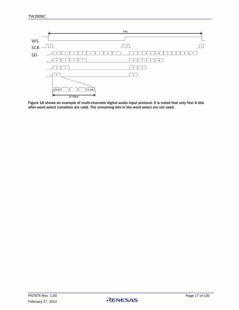
FIGURE 16. MULTI-CHANNEL DIGITAL AUDIO INTERFACE
SCK
WS
Edge detection
MSB LSB MSB LSBSD
Edge detection
Sample 0 Sample 1
FIGURE 15. I2S PROTOCOL
TW2809C
FN7875 Rev. 1.00 Page 17 of 130
February 27, 2014
Figure 16 shows an example of multi-channels digital audio input protocol. It is noted that only first 4 bits
after word select transition are valid. The remaining bits in the word select are not used.
TW2809C
FN7875 Rev. 1.00 Page 18 of 130
February 27, 2014
TW2809 Register Definition Overview
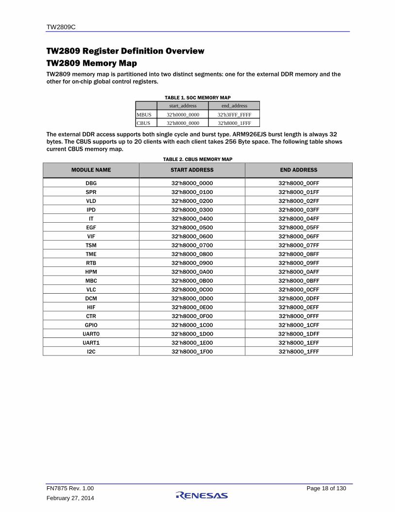
TW2809 Memory Map
TW2809 memory map is partitioned into two distinct segments: one for the external DDR memory and the
other for on-chip global control registers.
TABLE 1. SOC MEMORY MAP
start_address end_address
MBUS 32'h0000_0000 32'h3FFF_FFFF
CBUS 32'h8000_0000 32'h8000_1FFF
The external DDR access supports both single cycle and burst type. ARM926EJS burst length is always 32
bytes. The CBUS supports up to 20 clients with each client takes 256 Byte space. The following table shows
current CBUS memory map.
TABLE 2. CBUS MEMORY MAP
MODULE NAME START ADDRESS END ADDRESS
DBG 32'h8000_0000 32'h8000_00FF
SPR 32'h8000_0100 32'h8000_01FF
VLD 32'h8000_0200 32'h8000_02FF
IPD 32'h8000_0300 32'h8000_03FF
IT 32'h8000_0400 32'h8000_04FF
EGF 32'h8000_0500 32'h8000_05FF
VIF 32'h8000_0600 32'h8000_06FF
TSM 32'h8000_0700 32'h8000_07FF
TME 32'h8000_0800 32'h8000_08FF
RTB 32'h8000_0900 32'h8000_09FF
HPM 32'h8000_0A00 32'h8000_0AFF
MBC 32'h8000_0B00 32'h8000_0BFF
VLC 32'h8000_0C00 32'h8000_0CFF
DCM 32'h8000_0D00 32'h8000_0DFF
HIF 32'h8000_0E00 32'h8000_0EFF
CTR 32'h8000_0F00 32'h8000_0FFF
GPIO 32’h8000_1C00 32’h8000_1CFF
UART0 32’h8000_1D00 32’h8000_1DFF
UART1 32’h8000_1E00 32’h8000_1EFF
I2C 32’h8000_1F00 32’h8000_1FFF

TW2809C
FN7875 Rev. 1.00 Page 19 of 130
February 27, 2014
Interrupt Scheme The interrupt protocol is outlined in this section. By default, the first register of each hardware module should
be the register that defines the interrupt enable and status for the module.
INTERRUPT REGISTER
Address module base address + 0x00
Type r/w
31 30 29 28 27 26 25 24 23 22 21 20 19 18 17 16
status
15 14 13 12 11 10 9 8 7 6 5 4 3 2 1 0
enable
[31:17] reserved
[16] status – interrupt status. HW set this bit to HIGH to initiate interrupt. FW wirte HIGHT to clear
interrupt
[15:1] reserved
[0] enable – interrupt enable. 0: interrupt disable. 1: interrupt enable. Default is 1.
INTERRUPT PROTOCOL
HW generates an interrupt signal to FW when the interrupt source exist and the interrupt is enabled by the
FW. When FW detects the interrupt, it gets into interrupt service routine. When it is done, FW writes HIGH to
the status bit to clear the interrupt. When HW detects that FW is writing 1 to status bit, it shall clear the
interrupt source.

TW2809C
FN7875 Rev. 1.00 Page 20 of 130
February 27, 2014
PCI Register Definitions This section describes PCI module registers. Normally, any PCI core supports the following registers. TW2809
defines some value in the registers such as device ID, vendor ID, class code, and so on. If customers want to
know more detail information, they can check the configuration space section in “PCI local Bus Specification”
document.
TW2809C
FN7875 Rev. 1.00 Page 21 of 130
February 27, 2014
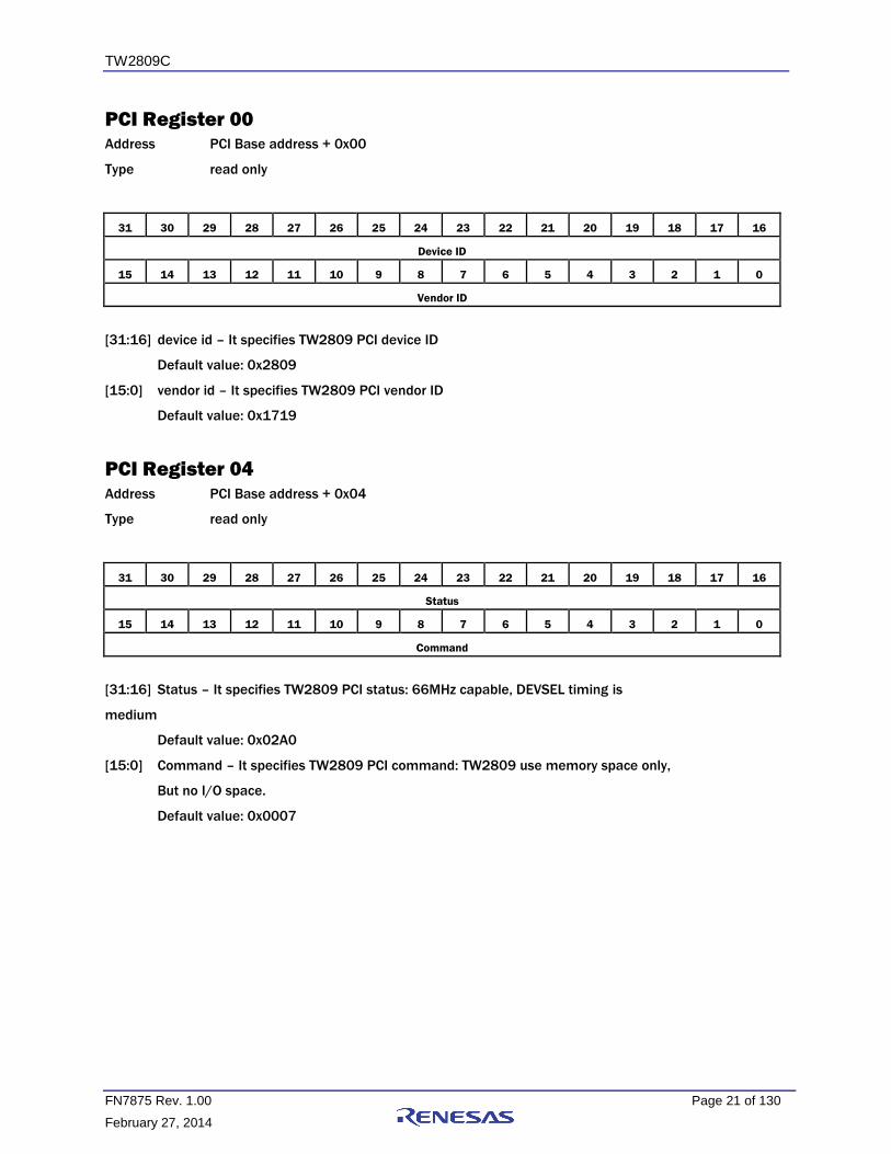
PCI Register 00 Address PCI Base address + 0x00
Type read only
31 30 29 28 27 26 25 24 23 22 21 20 19 18 17 16
Device ID
15 14 13 12 11 10 9 8 7 6 5 4 3 2 1 0
Vendor ID
[31:16] device id – It specifies TW2809 PCI device ID
Default value: 0x2809
[15:0] vendor id – It specifies TW2809 PCI vendor ID
Default value: 0x1719
PCI Register 04
Address PCI Base address + 0x04
Type read only
31 30 29 28 27 26 25 24 23 22 21 20 19 18 17 16
Status
15 14 13 12 11 10 9 8 7 6 5 4 3 2 1 0
Command
[31:16] Status – It specifies TW2809 PCI status: 66MHz capable, DEVSEL timing is
medium
Default value: 0x02A0
[15:0] Command – It specifies TW2809 PCI command: TW2809 use memory space only,
But no I/O space.
Default value: 0x0007

TW2809C
FN7875 Rev. 1.00 Page 22 of 130
February 27, 2014
PCI Register 08
Address PCI Base address + 0x08
Type read only
31 30 29 28 27 26 25 24 23 22 21 20 19 18 17 16
Class Code
15 14 13 12 11 10 9 8 7 6 5 4 3 2 1 0
Class Code Revision ID
[31:8] class code – It specifies TW2809 PCI class code
Default value: 0x048000
[7:0] Revision ID – It specifies TW2809 PCI revision ID
0: TW2809A1
1: TW2809B1
2: TW2809C1
PCI Register 0c Address PCI Base address + 0x0c
Type read only
31 30 29 28 27 26 25 24 23 22 21 20 19 18 17 16
BIST header type
15 14 13 12 11 10 9 8 7 6 5 4 3 2 1 0
latency timer cache line size
[31:24] BIST – It specifies TW2809 PCI BIST
Default value: 0x00
[23:16] header type – It specifies TW2809 PCI header type
Default value: 0x00
[15:8] latency timer – It specifies TW2809 PCI latency timer
Default value: 0x00
[7:0] cache line size – It specifies TW2809 PCI cache line size
Default value: 0x00

TW2809C
FN7875 Rev. 1.00 Page 23 of 130
February 27, 2014
PCI Register 10-24
Address PCI Base address + 0x10 – 0x24
Type read only
31 30 29 28 27 26 25 24 23 22 21 20 19 18 17 16
Base address registers
15 14 13 12 11 10 9 8 7 6 5 4 3 2 1 0
Register 10 (Bart #0) – TW2809 has 64K byte memory space
Register 14 (Bart #1) – Reserved
Register 18 (Bart #2) – Reserved
Register 1c (Bart #3) – Reserved
Register 20 (Bart #4) – Reserved
Register 24 (Bart #5) – Reserved
PCI Register 28
Address PCI Base address + 0x28
Type read only
31 30 29 28 27 26 25 24 23 22 21 20 19 18 17 16
Cardbus CIS Pointer
15 14 13 12 11 10 9 8 7 6 5 4 3 2 1 0
[31:0] Cardbus CIS Pointer – It specifies TW2809 PCI Cardbus CIS pointer
Default value: 0x00

TW2809C
FN7875 Rev. 1.00 Page 24 of 130
February 27, 2014
PCI Register 2c
Address PCI Base address + 0x2c
Type read only
31 30 29 28 27 26 25 24 23 22 21 20 19 18 17 16
Subsystem ID
15 14 13 12 11 10 9 8 7 6 5 4 3 2 1 0
Subsystem Vendor ID
[31:16] Subsystem id – It specifies TW2809 PCI subsystem ID
Default value: 0x2809
[15:0] Subsystem vendor id – It specifies TW2809 PCI subsystem vendor ID
Default value: 0x1719
PCI Register 30
Address PCI Base address + 0x30
Type read only
31 30 29 28 27 26 25 24 23 22 21 20 19 18 17 16
Expansion ROM Base Address
15 14 13 12 11 10 9 8 7 6 5 4 3 2 1 0
[31:0] Expansion ROM base address – It specifies TW2809 PCI expansion ROM base
address
Default value: 0x00

TW2809C
FN7875 Rev. 1.00 Page 25 of 130
February 27, 2014
PCI Register 34
Address PCI Base address + 0x34
Type read only
31 30 29 28 27 26 25 24 23 22 21 20 19 18 17 16
Reserved
15 14 13 12 11 10 9 8 7 6 5 4 3 2 1 0
Reserved Capabilities pointers
[31:8] Reserved
[7:0] Capabilities pointer – It specifies TW2809 PCI capabilities pointer
Default value: 0x00
PCI Register 38 Address PCI Base address + 0x38
Type read only
31 30 29 28 27 26 25 24 23 22 21 20 19 18 17 16
Reserved
15 14 13 12 11 10 9 8 7 6 5 4 3 2 1 0
[31:0] Reserved

TW2809C
FN7875 Rev. 1.00 Page 26 of 130
February 27, 2014
PCI Register 3c
Address PCI Base address + 0x3c
Type read only
31 30 29 28 27 26 25 24 23 22 21 20 19 18 17 16
Max_lat min grant
15 14 13 12 11 10 9 8 7 6 5 4 3 2 1 0
interrupt pin interrupt line
[31:24] max_lat– It specifies TW2809 PCI max_lat
Default value: 0x48
[23:16] min_gnt – It specifies TW2809 PCI min_gnt
Default value: 0x20
[15:8] interrupt pin – It specifies TW2809 PCI interrupt pin
Default value: 0x01
[7:0] interrupt line – It specifies TW2809 PCI interrupt line
Default value: 0x00

TW2809C
FN7875 Rev. 1.00 Page 27 of 130
February 27, 2014
Pin Mux Register Definitions This section describesTW2809 pin mux regsiter definitions. These regsiters shall be directly programmed by
external host during power up.
UART Pin Mux Configuration Address 0x8000_1404
Type r/w
31 30 29 28 27 26 25 24 23 22 21 20 19 18 17 16
dbg 15 14 13 12 11 10 9 8 7 6 5 4 3 2 1 0
[31] reserved
[30] dbg – It specifies chip debug mode. To enable uart, this bit shall be set to LOW.
[29:0] reserved
Address 0x8000_1408
Type r/w
31 30 29 28 27 26 25 24 23 22 21 20 19 18 17 16
uart1_en uart0_en mux_vo
15 14 13 12 11 10 9 8 7 6 5 4 3 2 1 0
[31:20] reserved
[19] uart1_en – It specifies pin mux control. To make pin H18 and H19 to be uart1, this bit shall be set to
HIGH.
[18] uart0_en – It specifies pin mux control. To make pin H20 and G17 to be uart0, this bit shall be set to
HIGH.
[17] mux_vo – It specifies pin mux control. To enable uart0/uart1, this bit shall be set to LOW.
[16:0] reserved
DESCRIPTIONS
Pin H20 and G17 is muxed by video input port 3 data bus [1:0] and uart0. In order to make these two pins to
be uart0. Pin H18 and H19 is muxed by video input port3 data bus[3:2]. In order to make these two pins to
be uart1, both register 0x8000_1404 and 0x8000_1408 need to be programmed.
Ball Num Symbol Pin Mux Mux condition
TW2809C UART1
H18 vi3_data[3] uart1_Tx 8000_1404[30] = 1'b0
8000_1408[17] = 1'b0
8000_1408[19] = 1'b1
H19 vi3_data[2] uart1_Rx 8000_1408[19] = 1'b1
TW2809C UART0
H20 vi3_data[1] uart0_Tx 8000_1404[30] = 1'b0
8000_1408[17] = 1'b0
8000_1408[18] = 1'b1
G17 vi3_data[0] uart0_Rx 8000_1408[18] = 1'b1

TW2809C
FN7875 Rev. 1.00 Page 28 of 130
February 27, 2014
GPIO[7:0] Pin Mux Configuration
Address 0x8000_1404
Type r/w
31 30 29 28 27 26 25 24 23 22 21 20 19 18 17 16
dbg
15 14 13 12 11 10 9 8 7 6 5 4 3 2 1 0
[31] reserved
[30] dbg – It specifies chip debug mode. To enable gpio[7:0], this bit shall be set to LOW.
[29:0] reserved
Address 0x8000_1408
Type r/w
31 30 29 28 27 26 25 24 23 22 21 20 19 18 17 16
gpio_en
15 14 13 12 11 10 9 8 7 6 5 4 3 2 1 0
[31:21] reserved
[20] gpio_en – It specifies pin mux control. To enable gpio[7:0], this bit shall be set to HIGH.
[19:0] reserved
DESCRIPTIONS
GPIO[7:0] is muxed with video output port 2. In order to enable gpio[7:0], both register 0x8000_1404 and
0x8000_1408 need to be programmed.
BALL NUM SYMBOL PIN MUX MUX CONDITION
W4 vo2_data[7] GPIO[7]
8000_1404[30] = 1'b0
8000_1408[20] = 1'b1
8000_1C40[7:0] controls GPIO direction
Output: 1'b1
Input: 1'b0
Y3 vo2_data[6] GPIO[6]
Y4 vo2_data[5] GPIO[5]
Y5 vo2_data[4] GPIO[4]
W5 vo2_data[3] GPIO[3]
V5 vo2_data[2] GPIO[2]
U5 vo2_data[1] GPIO[1]
Y6 vo2_data[0] GPIO[0]

TW2809C
FN7875 Rev. 1.00 Page 29 of 130
February 27, 2014
GPIO[15:8] Pin Mux Configuration
Address 0x8000_1400
Type r/w
31 30 29 28 27 26 25 24 23 22 21 20 19 18 17 16
mux_vi
15 14 13 12 11 10 9 8 7 6 5 4 3 2 1 0
[31] mux_vi – It specifies vi/vo mux mode. To enable gpio[15:8] and gipio[23:16], this bit shall
be set to LOW.
[30:0] reserved
Address 0x8000_1408
Type r/w
31 30 29 28 27 26 25 24 23 22 21 20 19 18 17 16
gpio_en
15 14 13 12 11 10 9 8 7 6 5 4 3 2 1 0
[31] gpio_en – It specifies pin mux control. To enable gpio[15:8], this bit shall be set to HIGH.
[30:0] reserved
DESCRIPTIONS
GPIO[15:8] is muxed with video output port 1. In order to enable gpio[15:8], both register 0x8000_1400 and
0x8000_1408 need to be programmed.
BALL NUM SYMBOL PIN MUX TW2809B MUX CONDITION
D18 vo1_data[7] GPIO[15] 8000_1400[31] = 1'b1
8000_1408[31] = 1'b1
8000_1C40[15:8] controls GPIO direction
Output: 1'b1
Input: 1'b0
D19 vo1_data[6] GPIO[14]
D20 vo1_data[5] GPIO[13]
C18 vo1_data[4] GPIO[12]
C19 vo1_data[3] GPIO[11]
C20 vo1_data[2] GPIO[10]
B19 vo1_data[1] GPIO[9]
B20 vo1_data[0] GPIO[8]

TW2809C
FN7875 Rev. 1.00 Page 30 of 130
February 27, 2014
GPIO[23:16] Pin Mux Configuration
Address 0x8000_1400
Type r/w
31 30 29 28 27 26 25 24 23 22 21 20 19 18 17 16
mux_vi
15 14 13 12 11 10 9 8 7 6 5 4 3 2 1 0
[31] mux_vi – It specifies vi/vo mux mode. To enable gpio[15:8] and gipio[23:16], this bit shall
be set to LOW.
[30:0] reserved
Address 0x8000_1408
Type r/w
31 30 29 28 27 26 25 24 23 22 21 20 19 18 17 16
gpio_en
15 14 13 12 11 10 9 8 7 6 5 4 3 2 1 0
[31] reserved
[30] gpio_en – It specifies pin mux control. To enable gipio[23:16], this bit shall be set to HIGH.
[29:0] reserved
DESCRIPTIONS
GPIO[23:16] is muxed with video output port 0. In order to enable gpio[23:16], both register 0x8000_1400
and 0x8000_1408 need to be programmed.
BALL NUM SYMBOL PIN MUX TW2809B MUX CONDITION
G19 vo0_data[7] GPIO[23] 8000_1400[31] = 1'b1
8000_1408[30] = 1'b1
8000_1C40[23:16] controls GPIO direction
Output: 1'b1
Input: 1'b0
F17 vo0_data[6] GPIO[22]
F18 vo0_data[5] GPIO[21]
F19 vo0_data[4] GPIO[20]
E18 vo0_data[3] GPIO[19]
E19 vo0_data[2] GPIO[18]
E20 vo0_data[1] GPIO[17]
D17 vo0_data[0] GPIO[16]

TW2809C
FN7875 Rev. 1.00 Page 31 of 130
February 27, 2014
GPIO[31:24] Pin Mux Configuration
Address 0x8000_1404
Type r/w
31 30 29 28 27 26 25 24 23 22 21 20 19 18 17 16
dbg
15 14 13 12 11 10 9 8 7 6 5 4 3 2 1 0
[31] reserved
[30] dbg – It specifies chip debug mode. To enable gpio[31:24], this bit shall be set to LOW.
[29:0] reserved
Address 0x8000_1408
Type r/w
31 30 29 28 27 26 25 24 23 22 21 20 19 18 17 16
uart1_en uart0_en mux_vo
15 14 13 12 11 10 9 8 7 6 5 4 3 2 1 0
[31:20] reserved
[19] uart1_en – It specifies pin mux control. To enable gpio[31:24], this bit shall be set to LOW.
[18] uart0_en – It specifies pin mux control. To enable gpio[31:24],, this bit shall be set to LOW..
[17] mux_vo – It specifies pin mux control To enable gpio[31:24],, this bit shall be set to LOW.
[16:0] reserved
Descriptions
GPIO[31:24] is muxed with video input port 3. In order to enable gpio[31:24], both register 0x8000_1404
and 0x8000_1408 need to be programmed.
BALL NUM SYMBOL PIN MUX TW2809B MUX CONDITION
K20 vi3_data[7] GPIO[31] 8000_1404[30] = 1'b0
8000_1408[19:17] = 3'b000
8000_1C40[31:24] controls GPIO direction
Output: 1'b1
Input: 1'b0
J18 vi3_data[6] GPIO[30]
J19 vi3_data[5] GPIO[29]
H17 vi3_data[4] GPIO[28]
H18 vi3_data[3] GPIO[27]
H19 vi3_data[2] GPIO[26]
H20 vi3_data[1] GPIO[25]
G17 vi3_data[0] GPIO[24]

TW2809C
FN7875 Rev. 1.00 Page 32 of 130
February 27, 2014
GPIO[39:32] pin mux configuration
Address 0x8000_1404
Type r/w
31 30 29 28 27 26 25 24 23 22 21 20 19 18 17 16
dbg
15 14 13 12 11 10 9 8 7 6 5 4 3 2 1 0
[31] reserved
[30] dbg – It specifies chip debug mode. To enable gpio[39:32], this bit shall be set to LOW.
[29:0] reserved
Address 0x8000_1408
Type r/w
31 30 29 28 27 26 25 24 23 22 21 20 19 18 17 16
mux_vo
15 14 13 12 11 10 9 8 7 6 5 4 3 2 1 0
[31:17] reserved
[16] mux_vo – It specifies pin mux control To enable gpio[39:32], this bit shall be set to LOW.
[15:0] reserved
DESCRIPTIONS
GPIO[39:32] is muxed with video input port 2. In order to enable gpio[39:32], both register 0x8000_1404
and 0x8000_1408 need to be programmed.
BALL NUM SYMBOL PIN MUX TW2809B MUX CONDITION
M18 vi2_data[7] GPIO[39] 8000_1404[30] = 1'b0
8000_1408[16] = 1'b0
8000_1C44[7:0] controls GPIO direction
Output: 1'b1
Input: 1'b0
M19 vi2_data[6] GPIO[38]
L17 vi2_data[5] GPIO[37]
L18 vi2_data[4] GPIO[36]
L19 vi2_data[3] GPIO[35]
K17 vi2_data[2] GPIO[34]
K18 vi2_data[1] GPIO[33]
K19 vi2_data[0] GPIO[32]

TW2809C
FN7875 Rev. 1.00 Page 33 of 130
February 27, 2014
GPIO[47:40] Pin Mux Configuration
Address 0x8000_1404
Type r/w
31 30 29 28 27 26 25 24 23 22 21 20 19 18 17 16
dbg
15 14 13 12 11 10 9 8 7 6 5 4 3 2 1 0
[31] reserved
[30] dbg – It specifies chip debug mode. To enable gpio[47:40], this bit shall be set to LOW.
[29:0] reserved
DESCRIPTIONS
GPIO[47:40] is muxed with video input port 1. In order to enable gpio[47:40], register 0x8000_1404 needs to
be programmed.
BALL NUM SYMBOL PIN MUX TW2809B MUX CONDITION
R19 vi1_data[7] GPIO[47] 8000_1404[30] = 1'b0
8000_1C44[15:8] controls GPIO direction
Output: 1'b1
Input: 1'b0
P17 vi1_data[6] GPIO[46]
P18 vi1_data[5] GPIO[45]
P19 vi1_data[4] GPIO[44]
N18 vi1_data[3] GPIO[43]
N19 vi1_data[2] GPIO[42]
N20 vi1_data[1] GPIO[41]
M17 vi1_data[0] GPIO[40]

TW2809C
FN7875 Rev. 1.00 Page 34 of 130
February 27, 2014
GPIO[55:48] pin mux configuration
Address 0x8000_1408
Type r/w
31 30 29 28 27 26 25 24 23 22 21 20 19 18 17 16
spi_e uart1_e gpio_e
15 14 13 12 11 10 9 8 7 6 5 4 3 2 1 0
[31:24] reserved
[23] spi_e – It specifies spi enable. To enable gpio[55:48], this bit shall be set to LOW.
[22] uart1_e – It specifies uart1 enable. To enable gpio[55:48], this bit shall be set to LOW.
[21] gpio_e – It specifies gpio enable. To enable gpio[55:48], this bit shall be set to HIGH.
[20:0] reserved
DESCRIPTIONS
GPIO[55:48] is muxed with video output port 3. In order to enable gpio[55:48], register 0x8000_1408 needs
to be programmed.
BALL NUM SYMBOL PIN MUX TW2809B MUX CONDITION
U9 vo3_data[7] GPIO[55] 8000_1408[23:21] = 3'b001
8000_1C44[23:16] controls GPIO direction
Output: 1'b1
Input: 1'b0
V8 vo3_data[6] GPIO[54]
U18 vo3_data[5] GPIO[53]
V18 vo3_data[4] GPIO[52]
U17 vo3_data[3] GPIO[51]
V19 vo3_data[2] GPIO[50]
W19 vo3_data[1] GPIO[49]
W20 vo3_data[0] GPIO[48]

TW2809C
FN7875 Rev. 1.00 Page 35 of 130
February 27, 2014
PDMA Register Definitions This section describes PDMA control module registers. PDMA has three kind of operation and is explained
seperately in this chapter.
Master Mode PDMA INTERRUPT STATUS REGISTER FOR FW
Address HIF base address + 0x48
Type r/w
31 30 29 28 27 26 25 24
DEBUG
_EN
SMBUS
ERR_INT_ST
MMBUS
ERR_INT_ST
23 22 21 20 19 18 17 16
SLV
INT_ST
PERR
INT_ST
FATAL
INT_ST
RX
INT_ST
TX
INT_ST
CFG
INT_ST
COM
INT_ST
15 14 13 12 11 10 9 8
- SMBUS
ERR_INT_EN
MMBUS
ERR_INT_EN
7 6 5 4 3 2 1 0
SLV
INT_EN
PERR
INT_EN
FATAL
INT_EN
M_RX
INT_EN
M_TX
INT_EN
CFG
INT_EN
COM
INT_EN
[31] DEBUG_EN – It specifies the debugging enable
[30:26] reserved
[25] SMBUS_ERR_INT_ST – It specifies the error of mbus for slave mode
[24] MMBUS_ERR_INT_ST – It specfies the error of mbus for master mode
[23] reserved
[22] SLV_INT_ST – It specifies the information of slave interrupt
[21] PERR_INT_ST – It specifies the information of PCI parity error interrupt.
[20] FATAL_INT_ST – It specifies the information of PCI fatal error interrupt.
[19] RX_INT_ST – It specifies the information of end of RX tranfer interrupt.
[18] TX_INT_ST – It specifies the information of end of TX transfer interrupt.
[17] CFG_INT_ST – It specifies the information of configuration interrupt.
[16] COM_INT_ST– It specifies the information of communcation interrupt.
[15:10] reserved
[09] SMBUS_ERR_INT_EN – It specifies the mbus error interrupt enable for slave mode
[08] MMBUS_ERR_INT_EN – It specifies the mbus error interrupt enable for master mode
[07] reserved
[06] SLV_INT_EN – It specifies the slave interrupt enable.
[05] PERR_INT_EN – It specifies parity error interrupt enable.
[04] FATAL_INT_EN – It specifies fatal error interrupt enable.
[03] M_RX_INT_EN – It specifies the end of RX transfer interrupt enable.
[02] M_TX_INT_EN – It specifies the end of TX transfer interrupt enable.
[01] CFG_INT_EN – It specifies the configuration interrupt enable.
[00] COM_INT_EN – It specifies the command interrupt enable.

TW2809C
FN7875 Rev. 1.00 Page 36 of 130
February 27, 2014
DESCRIPTIONS
PDMA supports to manage the interrupt sperately between FW and host driver. So the interrupt register is
only used by FW, not the host driver. Even if these interrupts are enabled and the host driver interrupts, which
address “0x4c” are disable in the same bit, PCI interrupt doesn’t generate to host driver, but it is sent to FW.
For example, FW enables TX transfer. Then, it means the end of TX transfer interrupt to be sent into FW, not
host driver.
In initial time, FW should enable PCI interrupt enable bits. If PCI interrupt enable bits are disabled, all of
interrupt except COM_INT_EN don’t generate the interrupt. Otherwise, PDMA can keep the interrupt when
PDMA generates the interrupt during COM_IN_EN to be disabled. Then PDMA will send the interrupt after
COM_IN_EN to be enabled.
PDMA MASTER TX AND RX INTERRUPT STATUS REGISTER (OPTIONAL)
Address HIF base address + 0x60
Type r
31 30 29 28 27 26 25 24 23 22 21 20 19 18 17 16
15 14 13 12 11 10 9 8 7 6 5 4 3 2 1 0
RX
END
TX
END
[31:02] reserved
[01] RX_END – It specifies end of RX transfer.
[00] TX_END – It specifies end of TX transfer
DESCRIPTIONS
This register isn’t used the normal operation. But sometimes FW or host driver doesn’t receive PDMA
interrupt after finishing the reading and writing data. In that time, FW or host driver could just check the end
of transfer using polling.

TW2809C
FN7875 Rev. 1.00 Page 37 of 130
February 27, 2014
PDMA MASTER TX AND RX ENDIAN CONTROL REGISTER
Address HIF Base address + 0x58
Type r/w
31 30 29 28 27 26 25 24 23 22 21 20 19 18 17 16
15 14 13 12 11 10 9 8 7 6 5 4 3 2 1 0
M_R_ENDIAN
[02:00]
M_W_ENDIAN
[02:00]
S_R_ENDIAN
[02:00]
S_W_ENDIAN
[02:00]
[31:15] reserved
[14:12] M_R_ENDIAN – It specifies the endian control of read data for master mode.
[11] reserved
[10:08] M_W_ENDIAN – It specifies the endian control of write data for master mode.
[07] reserved
[06:04] S_R_ENDIAN – It specifies the endian control of read data for slave mode.
[03] reserved
[02:00] S_W_ENDIAN – It specifies the endian control of write data for slave mode.
DESCRIPTIONS
Intel processor uses “little endian”, but TW2809 uses “big endian”. In the case host driver wants to change
little endian to big endian or big endian to little endian. So our PDMA is able to support it.
The following table bases on the 8 byte which our bus width is.
M_ENDIAN
OR
S_ENDIAN
DATA FORMAT
0 Data[63:00]
1 Data[39:32],Data[47:40],Data[55:48],Data[63:56],Data[07:00],Data[15:08],Data[23:16],Data[31:24]
2 Data[47:40],Data[39:32],Data[63:56],Data[55:48],Data[15:08],Data[07:00],Data[31:24],Data[23:16]
3 Data[31:24],Data[23:16],Data[15:08],Data[07:00],Data[63:56],Data[55:48],Data[47:40],Data[39:32]
4 Data[55:48],Data[63:56],Data[39:32],Data[47:40],Data[23:16],Data[31:24],Data[07:00],Data[15:08]
5 Data[07:00],Data[15:08],Data[23:16],Data[31:24],Data[39:32],Data[47:40],Data[55:48],Data[63:56]
6 Data[15:08],Data[07:00],Data[31:24],Data[23:16],Data[47:40],Data[39:32],Data[63:56],Data[55:48]
7 Data[23:16],Data[31:24],Data[07:00],Data[15:08],Data[55:48],Data[63:56],Data[39:32],Data[47:40]
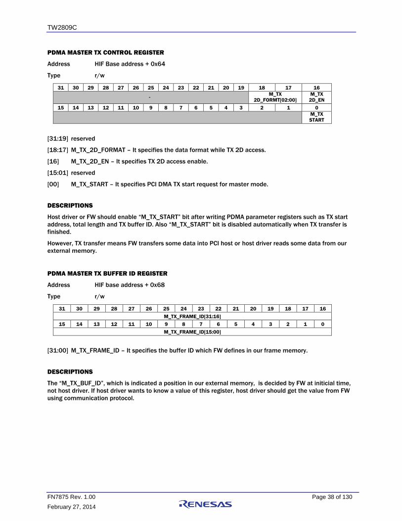
TW2809C
FN7875 Rev. 1.00 Page 38 of 130
February 27, 2014
PDMA MASTER TX CONTROL REGISTER
Address HIF Base address + 0x64
Type r/w
31 30 29 28 27 26 25 24 23 22 21 20 19 18 17 16
- M_TX
2D_FORMT[02:00]
M_TX
2D_EN
15 14 13 12 11 10 9 8 7 6 5 4 3 2 1 0
M_TX
START
[31:19] reserved
[18:17] M_TX_2D_FORMAT – It specifies the data format while TX 2D access.
[16] M_TX_2D_EN – It specifies TX 2D access enable.
[15:01] reserved
[00] M_TX_START – It specifies PCI DMA TX start request for master mode.
DESCRIPTIONS
Host driver or FW should enable “M_TX_START” bit after writing PDMA parameter registers such as TX start
address, total length and TX buffer ID. Also “M_TX_START” bit is disabled automatically when TX transfer is
finished.
However, TX transfer means FW transfers some data into PCI host or host driver reads some data from our
external memory.
PDMA MASTER TX BUFFER ID REGISTER
Address HIF base address + 0x68
Type r/w
31 30 29 28 27 26 25 24 23 22 21 20 19 18 17 16
M_TX_FRAME_ID[31:16]
15 14 13 12 11 10 9 8 7 6 5 4 3 2 1 0
M_TX_FRAME_ID[15:00]
[31:00] M_TX_FRAME_ID – It specifies the buffer ID which FW defines in our frame memory.
DESCRIPTIONS
The “M_TX_BUF_ID”, which is indicated a position in our external memory, is decided by FW at initicial time,
not host driver. If host driver wants to know a value of this register, host driver should get the value from FW
using communication protocol.
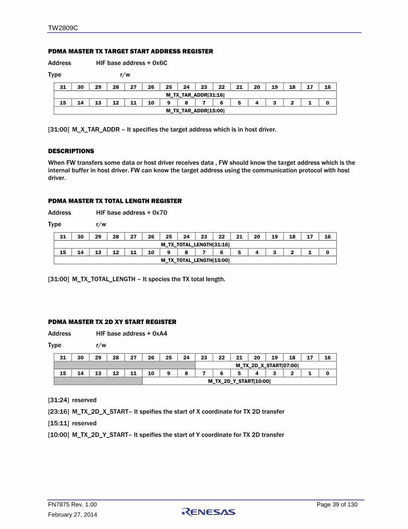
TW2809C
FN7875 Rev. 1.00 Page 39 of 130
February 27, 2014
PDMA MASTER TX TARGET START ADDRESS REGISTER
Address HIF base address + 0x6C
Type r/w
31 30 29 28 27 26 25 24 23 22 21 20 19 18 17 16
M_TX_TAR_ADDR[31:16]
15 14 13 12 11 10 9 8 7 6 5 4 3 2 1 0
M_TX_TAR_ADDR[15:00]
[31:00] M_X_TAR_ADDR – It specifies the target address which is in host driver.
DESCRIPTIONS
When FW transfers some data or host driver receives data , FW should know the target address which is the
internal buffer in host driver. FW can know the target address using the communication protocol with host
driver.
PDMA MASTER TX TOTAL LENGTH REGISTER
Address HIF base address + 0x70
Type r/w
31 30 29 28 27 26 25 24 23 22 21 20 19 18 17 16
M_TX_TOTAL_LENGTH[31:16]
15 14 13 12 11 10 9 8 7 6 5 4 3 2 1 0
M_TX_TOTAL_LENGTH[15:00]
[31:00] M_TX_TOTAL_LENGTH – It species the TX total length.
PDMA MASTER TX 2D XY START REGISTER
Address HIF base address + 0xA4
Type r/w
31 30 29 28 27 26 25 24 23 22 21 20 19 18 17 16
M_TX_2D_X_START[07:00]
15 14 13 12 11 10 9 8 7 6 5 4 3 2 1 0
M_TX_2D_Y_START[10:00]
[31:24] reserved
[23:16] M_TX_2D_X_START– It speifies the start of X coordinate for TX 2D transfer
[15:11] reserved
[10:00] M_TX_2D_Y_START– It speifies the start of Y coordinate for TX 2D transfer

TW2809C
FN7875 Rev. 1.00 Page 40 of 130
February 27, 2014
PDMA MASTER RX CONTROL REGISTER
Address HIF Base address + 0x78
Type r/w
31 30 29 28 27 26 25 24 23 22 21 20 19 18 17 16
M_RX_2D
FORMAT[02:00]
M_RX
2D_EN
15 14 13 12 11 10 9 8 7 6 5 4 3 2 1 0
M_RX
START
[31:19] reserved
[18:17] M_RX_2D_FORMAT – It specifies the data format for RX 2D transfer
[16] M_RX_2D_EN– It specifies RX 2D transfer enable.
[15:01] reserved
[00] M_RX_START – It specifies RX DMA start request.
DESCRIPTIONS
Host driver or FW can enable the bit, “M_RX_START”, after setting PDMA RX parameter registers such as TX
start address and total length. Also “M_RX_START” bit is disabled automatically by PDMA when TX transfer is
finished.
However, RX transfer means host driver writes some data into our external memory.
PDMA MASTER RX BUFFER ID REGISTER
Address HIF base address + 0x7C
Type r/w
31 30 29 28 27 26 25 24 23 22 21 20 19 18 17 16
M_RX_FRAME_ID[31:16]
15 14 13 12 11 10 9 8 7 6 5 4 3 2 1 0
M_RX_FRAME_ID[15:00]
[31:00] M_RX_FRAME_ID – It specifies the RX FRAME ID which FW defines in our frame memory.
DESCRIPTIONS
The “M_RX_BUF_ID”, which is indicated a buffer in our external memory, is decided by FW, not host driver at
initicial time. If host driver wants to know the value of “M_RX_BUF_ID”, host driver should get the value from
FW using commulation protocol.

TW2809C
FN7875 Rev. 1.00 Page 41 of 130
February 27, 2014
PDMA MASTER RX SOURCE START ADDRESS REGISTER
Address HIF base address + 0x80
Type r/w
31 30 29 28 27 26 25 24 23 22 21 20 19 18 17 16
M_RX_S_ADDR[31:16]
15 14 13 12 11 10 9 8 7 6 5 4 3 2 1 0
M_RX_S_ADDR[15:00]
[31:00] M_RX_S_ADDR – It specifies the source address which is the start address of internal buffer in host
driver.
DESCRIPTIONS
If host driver wants to send some data into our buffer or FW wants to read some data from host driver’s
buffer, FW or host driver set up “M_RX_S_ADDR” which is in host driver’s start buffer address. So FW should
gets the information from host driver using communication register.
PDMA MASTER RX TOTAL LENGTH REGISTER
Address HIF base address + 0x84
Type r/w
31 30 29 28 27 26 25 24 23 22 21 20 19 18 17 16
M_RX_TOTAL_LENGTH[31:16]
15 14 13 12 11 10 9 8 7 6 5 4 3 2 1 0
M_RX_TOTAL_LENGTH[15:00]
[31:00] M_RX_TOTAL_LENGTH – It species the RX total length.
PDMA MASTER RX 2D XY START REGISTER
Address HIF base address + 0xA8
Type r/w
31 30 29 28 27 26 25 24 23 22 21 20 19 18 17 16
M_RX_2D_X_START[07:00]
15 14 13 12 11 10 9 8 7 6 5 4 3 2 1 0
M_RX_2D_Y_START[10:00]
[31:24] reserved
[23:16] M_2D_RX_X_START– It speifies the start of X coordinate for RX 2D transfer
[10:00] M_2D_RX_Y_START– It speifies the start of Y coordinate for RX 2D transfer

TW2809C
FN7875 Rev. 1.00 Page 42 of 130
February 27, 2014
Slave Mode
HOST PCI driver should control registers for reading and writing.
PDMA SLAVE TX CONTROL REGISTER
Address HIF Base address + 0x24
Type r/w
31 30 29 28 27 26 25 24 23 22 21 20 19 18 17 16
S_TX_2D
FORMAT[01:00]
S_TX
2D_EN
15 14 13 12 11 10 9 8 7 6 5 4 3 2 1 0
S_TX_
STRN
S_TX
START
[31:19] reserved
[18:17] S_TX_2D_FORMAT – It specifies the data format while TX 2D access
[16] S_TX_2D_EN– It specifies TX 2D access enable
[15:05] reserved
[04] S_TX_STRN – It specifies the single tranfer enable
[03:01] reserved
[00] S_TX_START – It specifies DMA start request
DESCRIPTIONS
Currently, our host driver only supports the single tranfer, not burst transfer for slave mode.
If host driver uses the single transfer, PCI should enable “S_TX_STRN” bit.
Host driver or FW enables “S_TX_START” bit after finishing to write other TX setting registers such as TX start
address and length.
In addition, the performace is so slowly. Because PCI host driver is waiting to write data until receving PCI
interrupt after each 128 word transfer. This means PDMA internal buffer to be limited, 128 word.

TW2809C
FN7875 Rev. 1.00 Page 43 of 130
February 27, 2014
PDMA SLAVE TX BUFFER ID REGISTER
Address HIF base address + 0x28
Type r/w
31 30 29 28 27 26 25 24 23 22 21 20 19 18 17 16
15 14 13 12 11 10 9 8 7 6 5 4 3 2 1 0
S_TX_BUF_ID[05:00]
[31:06] reserved
[05:00] S_TX_BUF_ID – It specifies TX buffer ID
DESCRIPTIONS
The S_TX_BUF_ID, which is indicated a buffer ID in our external memory, is decided by FW, not PCI host
driver. So PCI host driver should get the buffer ID from FW using commulation protocol.
PDMA SLAVE TX TOTAL LENGTH REGISTER
Address HIF base address + 0x2c
Type r/w
31 30 29 28 27 26 25 24 23 22 21 20 19 18 17 16
S_TX_TOTAL_LENGTH[31:16]
15 14 13 12 11 10 9 8 7 6 5 4 3 2 1 0
S_TX_TOTAL_LENGTH[15:00]
[31:00] S_TX_TOTAL_LENGTH – It specifies the TX total length
DESCRIPTIONS
When PCI driver transfers some data into our external memory, PCI driver writes the total length, which is
word count, into the register.
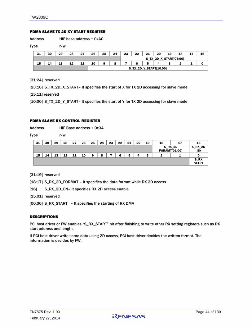
TW2809C
FN7875 Rev. 1.00 Page 44 of 130
February 27, 2014
PDMA SLAVE TX 2D XY START REGISTER
Address HIF base address + 0xAC
Type r/w
31 30 29 28 27 26 25 24 23 22 21 20 19 18 17 16
S_TX_2D_X_START[07:00]
15 14 13 12 11 10 9 8 7 6 5 4 3 2 1 0
S_TX_2D_Y_START[10:00]
[31:24] reserved
[23:16] S_TX_2D_X_START– It specifies the start of X for TX 2D accessing for slave mode
[15:11] reserved
[10:00] S_TX_2D_Y_START– It specifies the start of Y for TX 2D accessing for slave mode
PDMA SLAVE RX CONTROL REGISTER
Address HIF Base address + 0x34
Type r/w
31 30 29 28 27 26 25 24 23 22 21 20 19 18 17 16
S_RX_2D
FORAMT[01:00]
S_RX_2D
_EN
15 14 13 12 11 10 9 8 7 6 5 4 3 2 1 0
S_RX
START
[31:19] reserved
[18:17] S_RX_2D_FORMAT – It specifies the data format while RX 2D access
[16] S_RX_2D_EN– It specifies RX 2D access enable
[15:01] reserved
[00:00] S_RX_START – It specifies the starting of RX DMA
DESCRIPTIONS
PCI host driver or FW enables “S_RX_START” bit after finishing to write other RX setting registers such as RX
start address and length.
If PCI host driver write some data using 2D access, PCI host driver decides the written format. The
information is decides by FW.

TW2809C
FN7875 Rev. 1.00 Page 45 of 130
February 27, 2014
PDMA SLAVE RX BUFFER ID REGISTER
Address HIF base address + 0x38
Type r/w
31 30 29 28 27 26 25 24 23 22 21 20 19 18 17 16
15 14 13 12 11 10 9 8 7 6 5 4 3 2 1 0
S_R_BUF_ID[05:00]
[31:06] reserved
[05:00] S_R_BUF_ID – It specifies the external RX buffer ID
DESCRIPTIONS
The “S_R_BUF_ID”, which is one of buffer ID in our external memory, is decided by FW, not PCI host driver.
So PCI host driver should get the “S_R_BUF_ID” from FW using commulation protocol.
PDMA SLAVE RX TOTAL LENGTH REGISTER
Address HIF base address + 0x3c
Type r/w
31 30 29 28 27 26 25 24 23 22 21 20 19 18 17 16
S_RX_TOTAL_LENGTH[31:16]
15 14 13 12 11 10 9 8 7 6 5 4 3 2 1 0
S_RX_TOTAL_LENGTH[15:00]
[31:00] S_RX_TOTAL_LENGTH – It specifies the RX total length
DESCRIPTIONS
When PCI driver transfers some data into our external memory or FW receives some data from internal buffer
of PCI host driver, PCI driver writes the total length, which is word count, into the register.
PDMA SLAVE RX 2D XY START REGISTER
Address HIF base address + 0x88
Type r/w
31 30 29 28 27 26 25 24 23 22 21 20 19 18 17 16
S_RX_2D_X_START[07:00]
15 14 13 12 11 10 9 8 7 6 5 4 3 2 1 0
S_RX_2D_Y_START[10:00]
[31:24] reserved
[23:16] S_RX_2D_X_START– It specifies the start of X for RX 2D accessing for slave mode
[15:11] reserved
[10:00] S_RX_2D_Y_START– It specifies the start of Y for RX 2D accessing for slave mode

TW2809C
FN7875 Rev. 1.00 Page 46 of 130
February 27, 2014
PDMA SLAVE INTERRUPT STATUS REGISTER
Address HIF base address + 0x44
Type r
31 30 29 28 27 26 25 24 23 22 21 20 19 18 17 16
15 14 13 12 11 10 9 8 7 6 5 4 3 2 1 0
RX_
END
RX_
EMT
TX_
END
TX_
FULL
[31:04] reserved
[03] RX_END – It specifies the end of RX transfer
[02] RX_EMT– It specifies the empty of RX fifo
[01] TX_END – It specifies the end of TX transfer
[00] TX_FULL – It specifies the full of TX fifo
DESCRIPTIONS
Host driver or FW has to check PCI interrupt status register when host driver or FW receives PCI interrupt. If
“SLV_ST” bit in PCI interrupt status is asserted, host driver or FW should check data in this register. Then PCI
host or FW can know what kind of the interrupt for slave mode.

TW2809C
FN7875 Rev. 1.00 Page 47 of 130
February 27, 2014
Communication Between FW and Host
These registers are used to communicate between FW and host driver.
In the further, FW and Host driver will be decided some commands for proper processing.
THE COMMUNICATION COMMAND REGISTER FROM HOST DRIVER
Address HIF base address + 0x8C
Type r/w
31 30 29 28 27 26 25 24 23 22 21 20 19 18 17 16
CMD_FROM_HOST[31:16]
15 14 13 12 11 10 9 8 7 6 5 4 3 2 1 0
CMD_FROM_HOST[15:00]
[31:00] CMD_FROM_HOST– It specifies a communication command which host driver sends into
FW.
DESCRIPTIONS
PDMA generates the interrupt to FW when host driver writes a command in this register. FW will operate the
proper task after reading data in the PCI interrupt serive rountine of FW.
For example, host driver sends a command which is ready the decoding bitstream after sending the decoding
bitstream into a external VLD buffer of TW2809. In that time, host driver uses this register.
THE FIRST EXTRA COMMUNICATION REGISTER FROM HOST DRIVER
Address HIF base address + 0x54
Type r/w
31 30 29 28 27 26 25 24 23 22 21 20 19 18 17 16
CMD_EXTRA1_FROM_HOST[31:16]
15 14 13 12 11 10 9 8 7 6 5 4 3 2 1 0
CMD_EXTRA1_FROM_HOST[15:00]
[31:00] CMD_EXTRA1_FROM_HOST – It specifies the first extra communication
data
DESCRIPTIONS
Sometimes, host driver needs to have the first extra data with a command. In that time, host driver uses the
register. Host driver has to write the register before writing the communication register, “Communication
Register from Host”.
For example, host driver wants to send the command, which is the bitstream size, after sending the bitstream
for decoding. In that time, host driver writes the bitstream size into this register. Then FW can know the
bitstream size after reading this register.

TW2809C
FN7875 Rev. 1.00 Page 48 of 130
February 27, 2014
THE SECOND EXTRA COMMUNICATION REGISTER FROM HOST DRIVER
Address HIF base address + 0x58
Type r/w
31 30 29 28 27 26 25 24 23 22 21 20 19 18 17 16
CMD_EXTRA2_FROM_HOST[31:16]
15 14 13 12 11 10 9 8 7 6 5 4 3 2 1 0
CMD_EXTRA2_FROM_HOST[15:00]
[31:00] CMD_EXTRA2_FROM_HOST – It specifies the second extra communication
data
THE COMMUNICATION COMMAND REGISTER FROM FW
Address HIF base address + 0x90
Type r/w
31 30 29 28 27 26 25 24 23 22 21 20 19 18 17 16
CMD_FROM_FW[31:16]
15 14 13 12 11 10 9 8 7 6 5 4 3 2 1 0
CMD_FROM_FW[15:00]
[31:00] CMD_FROM_FW – It specifies a communication command which FW sends into host.
DESCRIPTIONS
PDMA’s able to generate the the interrupt to host driver when FW writes this register. After that, host driver
will operate the proper task after reading the command.
For example, FW wants to recevice a bitstream of slice for decoding. In that time, FW writes a command into
the register. And host driver recevices the command. Then, host driver will download the bitstream into
external VLD buffer of TW2809. In the futher, FW and host driver will define the value of command.

TW2809C
FN7875 Rev. 1.00 Page 49 of 130
February 27, 2014
THE FIRST EXTRA COMMUNICATION REGISTER FROM FW
Address HIF base address + 0x94
Type r/w
31 30 29 28 27 26 25 24 23 22 21 20 19 18 17 16
EXTRA1_COM_FROM_FW[31:16]
15 14 13 12 11 10 9 8 7 6 5 4 3 2 1 0
EXTRA1_COM_FROM_FW[15:00]
[31:00] EXTRA1_COM_ FROM_FW– It specifies the first extra communication data.
DESCRIPTIONS
Sometimes, FW needs to have extra data with a command. In that time, FW uses current register. FW has to
write the register before writing the commnication register, “Communication Register from FW”.
For example, FW sends the command, which is the request bitstream, to host driver. In that time, FW also
send a buffer ID which is defined the external VLD buffer. Then FW writes the buffer ID into the register.
Therefore host driver can know buffer ID after reading this register.
THE SECOND EXTRA COMMUNICATION REGISTER FROM FW
Address HIF base address + 0x98
Type r/w
31 30 29 28 27 26 25 24 23 22 21 20 19 18 17 16
EXTRA2_COM_FROM_FW[31:16]
15 14 13 12 11 10 9 8 7 6 5 4 3 2 1 0
EXTRA2_COM_FROM_FW[15:00]
[31:00] EXTRA2_COM_FROM_FW – It specifies the second extra communication
data
DESCRIPTIONS
Sometimes, FW needs to have extra data with a communication command. In that time, FW uses the
register. FW has to write the register before writing the communication register, “Communication Command
Register from FW”.
For example, FW wants to send the command, which is the end of encoding, to host driver. In that time, FW
also send the buffer ID which is defined in external VLC buffer, and a total length which is the bitstream size
of current slice. Then FW uses extra #1 and #2 register. FW write the buffer ID into the register, “The First
Communication Extra Register from FW”. Also current register is written the total length.

TW2809C
FN7875 Rev. 1.00 Page 50 of 130
February 27, 2014
Interrupt Status for PCI Host Driver
PCI Host should read this registers when it receives PCI interrupt from TW2809.
PDMA INTERRUPT STATUS REGISTER FOR PCI CHANNEL
Address HIF base address + 0x4C
Type r/w
31 30 29 28 27 26 25 24
INT_
EDGE_EN
SMBUS_
ERR_INT_ST
MMBUS_
ERR_INT_ST
23 22 21 20 19 18 17 16
WDOG_
INT_ST
SLV_
INT_ST
PERR_
INT_ST
FATAL_
INT_ST
RX_
INT_ST
TX_
INT_ST
CFG_
INT_ST
COM_
INT_ST
15 14 13 12 11 10 9 8
SMBUS_
ERR_INT_EN
MMBUS_
ERR_INT_EN
7 6 5 4 3 2 1 0
WDOG_
INT_EN
SLV_
INT_EN
PERR_
INT_EN
FATAL_
INT_EN
RX_
INT_EN
TX_
INT_EN
CFG_
INT_EN
COM_
INT_EN
[31] INT_EDGE_EN – It specfies the edge trigger interrupt.
[30:26] reserved
[25] SMBUS_ERR_INT_ST – It specfies the error of mbus for slave mode
[24] MMBUS_ERR_INT_ST – It specfies the error of mbus for master mode
[23] WDOG_INT_ST – It specfies the information of watch dog.
[22] SLV_INT_ST – It specfies the interrupt for slave mode (debug mode)
[21] PERR_INT_ST – It specifies the information of parity error interrupt.
[20] FATAL_INT_ST – It specfies the information of fatal error interrupt.
[19] RX_INT_ST – It specifies the information of end of RX transfer.
[18] TX_INT_ST – It specifies the information of end of TX transfer.
[17] CFG_INT_ST – It specifies the information of config interrupt.
[16] COM_INT_ST – It specifies the information of command interrupt.
[15:10] reserved
[09] SMBUS_ERR_INT_EN – It specfies the mbus error interrupt enable for slave mode
[08] MMBUS_ERR_INT_EN – It specfies the mbus error interrupt enable for master mode
[07] WDOG_INT_EN – It specifies watch dog interrupt enable.
[06] SLV_INT_EN – It specifies slave mode interrupt enable.
[05] PERR_INT_EN – It specifies PCI parity error interrupt enable.
[04] FATAL_INT_EN – It specifies PCI fatal error interrupt enable.
[03] RX_INT_EN – It specifies RX END interrupt enable.
[02] TX_INT_EN – It specifies TX END interrupt enable.
[01] CFG_INT_EN – It specifies Configuration interrupt enable.
[00] COM_INT_EN – It specifies Command interrupt enable.
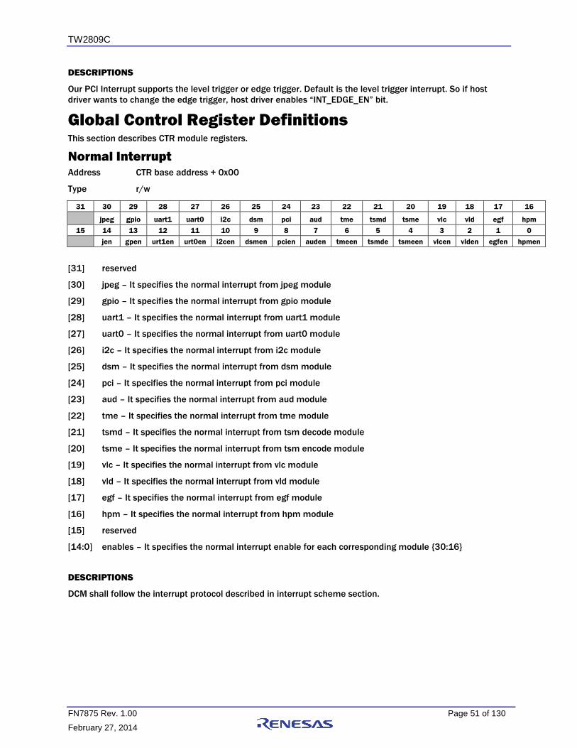
TW2809C
FN7875 Rev. 1.00 Page 51 of 130
February 27, 2014
DESCRIPTIONS
Our PCI Interrupt supports the level trigger or edge trigger. Default is the level trigger interrupt. So if host
driver wants to change the edge trigger, host driver enables “INT_EDGE_EN” bit.
Global Control Register Definitions This section describes CTR module registers.
Normal Interrupt Address CTR base address + 0x00
Type r/w
31 30 29 28 27 26 25 24 23 22 21 20 19 18 17 16
jpeg gpio uart1 uart0 i2c dsm pci aud tme tsmd tsme vlc vld egf hpm
15 14 13 12 11 10 9 8 7 6 5 4 3 2 1 0
jen gpen urt1en urt0en i2cen dsmen pcien auden tmeen tsmde tsmeen vlcen vlden egfen hpmen
[31] reserved
[30] jpeg – It specifies the normal interrupt from jpeg module
[29] gpio – It specifies the normal interrupt from gpio module
[28] uart1 – It specifies the normal interrupt from uart1 module
[27] uart0 – It specifies the normal interrupt from uart0 module
[26] i2c – It specifies the normal interrupt from i2c module
[25] dsm – It specifies the normal interrupt from dsm module
[24] pci – It specifies the normal interrupt from pci module
[23] aud – It specifies the normal interrupt from aud module
[22] tme – It specifies the normal interrupt from tme module
[21] tsmd – It specifies the normal interrupt from tsm decode module
[20] tsme – It specifies the normal interrupt from tsm encode module
[19] vlc – It specifies the normal interrupt from vlc module
[18] vld – It specifies the normal interrupt from vld module
[17] egf – It specifies the normal interrupt from egf module
[16] hpm – It specifies the normal interrupt from hpm module
[15] reserved
[14:0] enables – It specifies the normal interrupt enable for each corresponding module {30:16}
DESCRIPTIONS
DCM shall follow the interrupt protocol described in interrupt scheme section.

TW2809C
FN7875 Rev. 1.00 Page 52 of 130
February 27, 2014
Codec Video Channel
Address CTR base address + 0x04
Type r/w
31 30 29 28 27 26 25 24 23 22 21 20 19 18 17 16
cur_dec_ch
15 14 13 12 11 10 9 8 7 6 5 4 3 2 1 0
cur_enc_ch
[31:21] reserved
[20:16] cur_dec_ch – It specifies current decode video channel
[15:5] reserved
[4:0] cur_enc_ch – It specifies current encode video channel
DESCRIPTIONS
DCM shall follow the interrupt protocol described in interrupt scheme section.
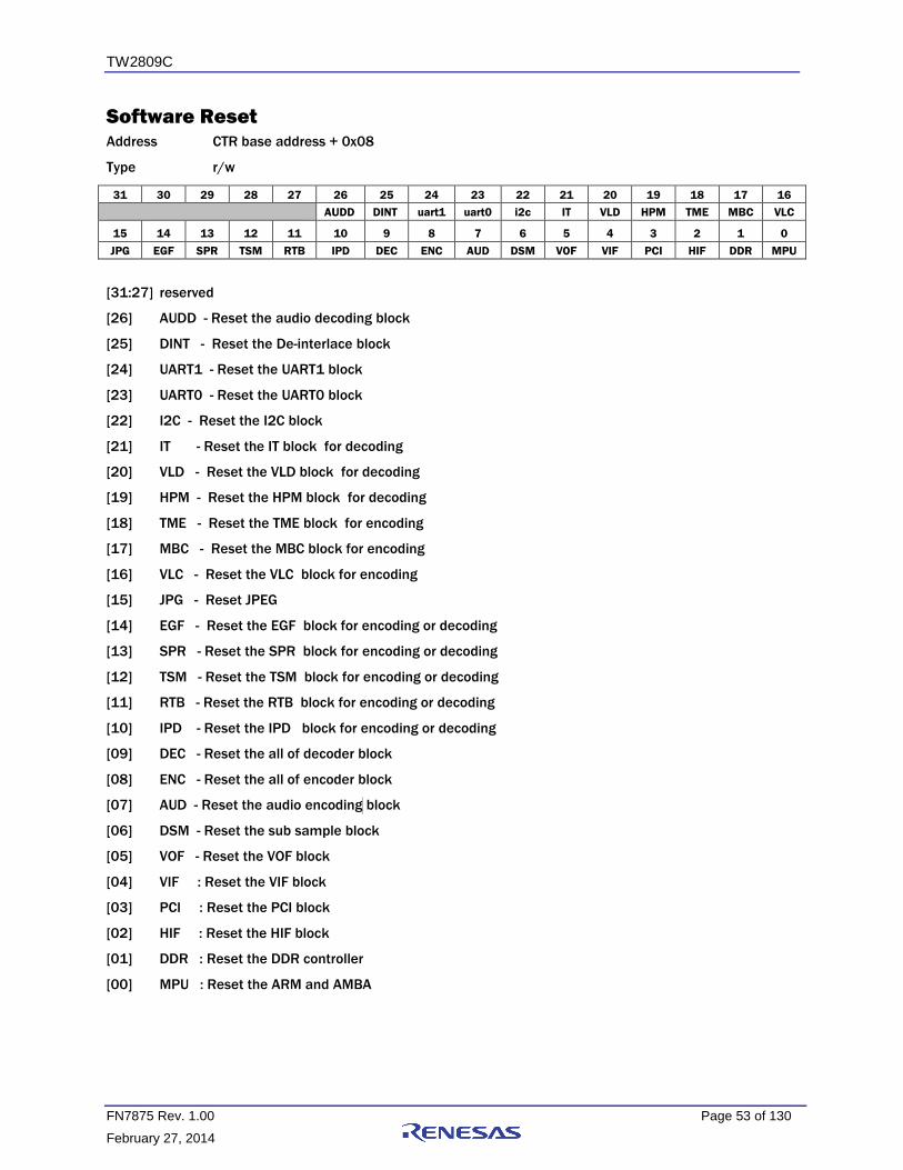
TW2809C
FN7875 Rev. 1.00 Page 53 of 130
February 27, 2014
Software Reset
Address CTR base address + 0x08
Type r/w
31 30 29 28 27 26 25 24 23 22 21 20 19 18 17 16
AUDD DINT uart1 uart0 i2c IT VLD HPM TME MBC VLC
15 14 13 12 11 10 9 8 7 6 5 4 3 2 1 0
JPG EGF SPR TSM RTB IPD DEC ENC AUD DSM VOF VIF PCI HIF DDR MPU
[31:27] reserved
[26] AUDD - Reset the audio decoding block
[25] DINT - Reset the De-interlace block
[24] UART1 - Reset the UART1 block
[23] UART0 - Reset the UART0 block
[22] I2C - Reset the I2C block
[21] IT - Reset the IT block for decoding
[20] VLD - Reset the VLD block for decoding
[19] HPM - Reset the HPM block for decoding
[18] TME - Reset the TME block for encoding
[17] MBC - Reset the MBC block for encoding
[16] VLC - Reset the VLC block for encoding
[15] JPG - Reset JPEG
[14] EGF - Reset the EGF block for encoding or decoding
[13] SPR - Reset the SPR block for encoding or decoding
[12] TSM - Reset the TSM block for encoding or decoding
[11] RTB - Reset the RTB block for encoding or decoding
[10] IPD - Reset the IPD block for encoding or decoding
[09] DEC - Reset the all of decoder block
[08] ENC - Reset the all of encoder block
[07] AUD - Reset the audio encoding block
[06] DSM - Reset the sub sample block
[05] VOF - Reset the VOF block
[04] VIF : Reset the VIF block
[03] PCI : Reset the PCI block
[02] HIF : Reset the HIF block
[01] DDR : Reset the DDR controller
[00] MPU : Reset the ARM and AMBA

TW2809C
FN7875 Rev. 1.00 Page 54 of 130
February 27, 2014
DESCRIPTION
This register is used to control the TW2809 reset. Host or FW write LOW to assert tw2809 blocks reset. Host
or FW write HIGH to release the reset.
If you want to assert reset to all of encoder block, you write LOW into “ENC” bit.
Then, all of encoder blocks will be asserted the reset. also you write LOW into “DEC” bit, all of decoder blocks
will be asserted the reset.
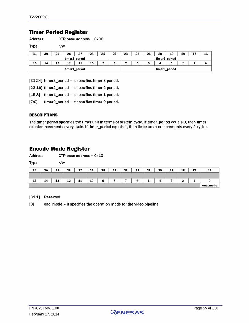
TW2809C
FN7875 Rev. 1.00 Page 55 of 130
February 27, 2014
Timer Period Register
Address CTR base address + 0x0C
Type r/w
31 30 29 28 27 26 25 24 23 22 21 20 19 18 17 16
timer3_period timer2_period
15 14 13 12 11 10 9 8 7 6 5 4 3 2 1 0
timer1_period timer0_period
[31:24] timer3_period – It specifies timer 3 period.
[23:16] timer2_period – It specifies timer 2 period.
[15:8] timer1_period – It specifies timer 1 period.
[7:0] timer0_period – It specifies timer 0 period.
DESCRIPTIONS
The timer period specifies the timer unit in terms of system cycle. If timer_period equals 0, then timer
counter increments every cycle. If timer_period equals 1, then timer counter increments every 2 cycles.
Encode Mode Register
Address CTR base address + 0x10
Type r/w
31 30 29 28 27 26 25 24 23 22 21 20 19 18 17 16
15 14 13 12 11 10 9 8 7 6 5 4 3 2 1 0
enc_mode
[31:1] Reserved
[0] enc_mode – It specifies the operation mode for the video pipeline.

TW2809C
FN7875 Rev. 1.00 Page 56 of 130
February 27, 2014
Fast Interrupt Address CTR base address + 0x14
Type r/w
31 30 29 28 27 26 25 24 23 22 21 20 19 18 17 16
timer0 timer1 timer2 timer3 vout vin
15 14 13 12 11 10 9 8 7 6 5 4 3 2 1 0
t0en t1en t2en t3en voen vien
[31] timer0 – It specifies the fast interrupt from timer0
[30] timer1 – It specifies the fast interrupt from timer1
[29] timer2 – It specifies the fast interrupt from timer2
[28] timer3 – It specifies the fast interrupt from timer 3
[27:18] reserved
[17] vout – It specifies the fast interrupt from VOUT module
[16] vin – It specifies the fast interrupt from VIN module
[12:2] reserved – It specifies the fast interrupt source.
[15] t0en – It specifies the fast interrupt enable for timer0
[14] t1en – It specifies the fast interrupt enable for timer1
[13] t2en – It specifies the fast interrupt enable for timer2
[12] t3en – It specifies the fast interrupt enable for timer3
[11:2] reserved
[1] voen – It specifies the fast interrupt enable for VOUT module
[0] vien – It specifies the fast interrupt enable for VIN module
DESCRIPTIONS
DCM shall follow the interrupt protocol described in interrupt scheme section.

TW2809C
FN7875 Rev. 1.00 Page 57 of 130
February 27, 2014
Encoder Parameter Register 0
Address CTR base address + 0x20
Type r/w
31 30 29 28 27 26 25 24 23 22 21 20 19 18 17 16
vertical_size
15 14 13 12 11 10 9 8 7 6 5 4 3 2 1 0
horizontal_size
[31:27] Reserved
[26:16] vertical_size – It specifies video vertical size in pixel.
[15:11] Reserved
[10:0] horizontal_size – It specifies video horizontal size in pixel.
Encoding Parameter Register 1 Address CTR base address + 0x24
Type r/w
31 30 29 28 27 26 25 24 23 22 21 20 19 18 17 16
rc_type bframe_num prog Initial_QP
15 14 13 12 11 10 9 8 7 6 5 4 3 2 1 0
frame_rate IDRPeriod
[31:30] rc_type – video rate control type: 00 – CQP, 01-CBR, 10- VBR, 11- HBR
[29:28] bframe_num – It specifies how many b frames between two reference frame
[27] prog – It specifies if curren video sequence is progressive video.
1- progressive video
0 – interleaved video
[26:16] Initial_QP – It specifies initial QP for the video encoding
[15:8] frame_rate – It specifies encoding frame rate
[7:0] IDRPeriod – It specifies IDR distance in terms of frame count

TW2809C
FN7875 Rev. 1.00 Page 58 of 130
February 27, 2014
Encoder Parameter Register 2
Address CTR base address + 0x28
Type r/w
31 30 29 28 27 26 25 24 23 22 21 20 19 18 17 16
15 14 13 12 11 10 9 8 7 6 5 4 3 2 1 0
video_bit_rate
[31:16] reserved
[15:0] video_bit_rate – It specifies current video sequence encoding bit rate in terms of Kbps
Encoder Parameter Register 3
Address CTR base address + 0x2c
Type r/w
31 30 29 28 27 26 25 24 23 22 21 20 19 18 17 16
lp_flag lp_dis Loopfilter_AlphaOffset
15 14 13 12 11 10 9 8 7 6 5 4 3 2 1 0
Loopfilter_BeltaOffset
[31] lp_flag
[30] lp_dis – It specifies loop filter disable
[29:24] reserved
[23:16] Loopfilter_AlphaOffset
[15:8] reserved
[7:0] Loopfilter_BeltaOffset

TW2809C
FN7875 Rev. 1.00 Page 59 of 130
February 27, 2014
Timer 0 Count
Address CTR base address + 0x30
Type r/w
31 30 29 28 27 26 25 24 23 22 21 20 19 18 17 16
timer_count
15 14 13 12 11 10 9 8 7 6 5 4 3 2 1 0
[31:0] timer_count – It specifies timer value
Timer 1 Count
Address CTR base address + 0x34
Type r/w
31 30 29 28 27 26 25 24 23 22 21 20 19 18 17 16
timer_count
15 14 13 12 11 10 9 8 7 6 5 4 3 2 1 0
[31:0] timer_count – It specifies timer value
Timer 2 Count Address CTR base address + 0x38
Type r/w
31 30 29 28 27 26 25 24 23 22 21 20 19 18 17 16
timer_count
15 14 13 12 11 10 9 8 7 6 5 4 3 2 1 0
[31:0] timer_count – It specifies timer value
Timer 3 Count
Address CTR base address + 0x3c
Type r/w
31 30 29 28 27 26 25 24 23 22 21 20 19 18 17 16
timer_count
15 14 13 12 11 10 9 8 7 6 5 4 3 2 1 0
[31:0] timer_count – It specifies timer value

TW2809C
FN7875 Rev. 1.00 Page 60 of 130
February 27, 2014
Encoder Parameter Register 4
Address CTR base address + 0x40
Type r/w
31 30 29 28 27 26 25 24 23 22 21 20 19 18 17 16
lp_flag
15 14 13 12 11 10 9 8 7 6 5 4 3 2 1 0
[31:0] lp_flag
Descriptions:
Please refer to TW2809 SW user manual for more details on how to set encoder paramters.
Encoder Parameter Register 5
Address CTR base address + 0x44
Type r/w
31 30 29 28 27 26 25 24 23 22 21 20 19 18 17 16
lp_flag
15 14 13 12 11 10 9 8 7 6 5 4 3 2 1 0
[31:0] lp_flag-
Descriptions:
Please refer to TW2809 SW user manual for more details on how to set encoder paramters.

TW2809C
FN7875 Rev. 1.00 Page 61 of 130
February 27, 2014
Encoder Parameter Register 6
Address CTR base address + 0x48
Type r/w
31 30 29 28 27 26 25 24 23 22 21 20 19 18 17 16
lp_flag
15 14 13 12 11 10 9 8 7 6 5 4 3 2 1 0
[31:0] lp_flag
Descriptions:
Please refer to TW2809 SW user manual for more details on how to set encoder paramters.
Encoder Parameter Register 7
Address CTR base address + 0x4c
Type r/w
31 30 29 28 27 26 25 24 23 22 21 20 19 18 17 16
lp_flag
15 14 13 12 11 10 9 8 7 6 5 4 3 2 1 0
[31:0] lp_flag
Descriptions:
Please refer to TW2809 SW user manual for more details on how to set encoder paramters.
Encoder Parameter Register 8
Address CTR base address + 0x50
Type r/w
31 30 29 28 27 26 25 24 23 22 21 20 19 18 17 16
lp_flag
15 14 13 12 11 10 9 8 7 6 5 4 3 2 1 0
[31:0] lp_flag
Descriptions:
Please refer to TW2809 SW user manual for more details on how to set encoder paramters.

TW2809C
FN7875 Rev. 1.00 Page 62 of 130
February 27, 2014
Encoder Parameter Register 9
Address CTR base address + 0x54
Type r/w
31 30 29 28 27 26 25 24 23 22 21 20 19 18 17 16
lp_flag
15 14 13 12 11 10 9 8 7 6 5 4 3 2 1 0
[31:0] lp_flag -
Descriptions:
Please refer to TW2809 SW user manual for more details on how to set encoder paramters.
Encoder Parameter Register 10
Address CTR base address + 0x58
Type r/w
31 30 29 28 27 26 25 24 23 22 21 20 19 18 17 16
lp_flag
15 14 13 12 11 10 9 8 7 6 5 4 3 2 1 0
[31:0] lp_flag
Descriptions:
Please refer to TW2809 SW user manual for more details on how to set encoder paramters.

TW2809C
FN7875 Rev. 1.00 Page 63 of 130
February 27, 2014
Encoder Parameter Register 11
Address CTR base address + 0x5c
Type r/w
31 30 29 28 27 26 25 24 23 22 21 20 19 18 17 16
lp_flag
15 14 13 12 11 10 9 8 7 6 5 4 3 2 1 0
[31:0] lp_flag
Descriptions:
Please refer to TW2809 SW user manual for more details on how to set encoder paramters.
Encoder Parameter Register 12 Address CTR base address + 0x60
Type r/w
31 30 29 28 27 26 25 24 23 22 21 20 19 18 17 16
lp_flag
15 14 13 12 11 10 9 8 7 6 5 4 3 2 1 0
[31:0] lp_flag
Descriptions:
Please refer to TW2809 SW user manual for more details on how to set encoder paramters.
Watch Dog Limit
Address CTR base address + 0x64
Type r/w
31 30 29 28 27 26 25 24 23 22 21 20 19 18 17 16
watch_dog_limit
15 14 13 12 11 10 9 8 7 6 5 4 3 2 1 0
[31:0] watch_dog_limit – It species the watch dog interrupt counter value. If watch dog counter reaches this
value, it will raise interrupt to host.

TW2809C
FN7875 Rev. 1.00 Page 64 of 130
February 27, 2014
Timer Control Register
Address CTR base address + 0x68
Type r/w
31 30 29 28 27 26 25 24 23 22 21 20 19 18 17 16
wdg_en go3 go2 go1 go0
15 14 13 12 11 10 9 8 7 6 5 4 3 2 1 0
hold3 hold2 hold1 hold0
[31] wdg_en – It species watch dog enable
[30:20] reserved
[19] go3 – It species timer3 control go signal
[18] go2 – It species timer2 control go signal
[17] go1 – It species timer1 control go signal
[16] go0 – It species timer0 control go signal
[15:4] reserved
[3] hold3 – It species timer3 control hold signal
[2] hold2 – It species timer2 control hold signal
[1] hold1 – It species timer1 control hold signal
[0] hold0 – It species timer0 control hold signal
DESCRIPTIONS
hold – It species timer hold control. This is a level control signal
0 : counter is disabled and held in the current state
1: counter is allowed to count
go – It resets and starts the timer counter. This is a pulse control register
0 : no effets on the timers
1: if hold is HIGHT, the counter register is zeroed and begins counting on the next clock.

TW2809C
FN7875 Rev. 1.00 Page 65 of 130
February 27, 2014
Timer 1 Control Register
Address CTR base address + 0x44
Type r/w
31 30 29 28 27 26 25 24 23 22 21 20 19 18 17 16
15 14 13 12 11 10 9 8 7 6 5 4 3 2 1 0
hold go
[31:2] reserved
[1] hold – It species timer hold control. This is a level control signal
0 : counter is disabled and held in the current state
1: counter is allowed to count
[0] go – It resets and starts the timer counter. This is a pulse control register
0 : no effets on the timers
1: if hold is HIGHT, the counter register is zeroed and begins counting on the next clock.
Timer 2 Control Register Address CTR base address + 0x48
Type r/w
31 30 29 28 27 26 25 24 23 22 21 20 19 18 17 16
15 14 13 12 11 10 9 8 7 6 5 4 3 2 1 0
hold go
[31:2] reserved
[1] hold – It species timer hold control. This is a level control signal
0 : counter is disabled and held in the current state
1: counter is allowed to count
[0] go – It resets and starts the timer counter. This is a pulse control register
0 : no effets on the timers
1: if hold is HIGHT, the counter register is zeroed and begins counting on the next clock.

TW2809C
FN7875 Rev. 1.00 Page 66 of 130
February 27, 2014
Timer 3 Control Register
Address CTR base address + 0x4c
Type r/w
31 30 29 28 27 26 25 24 23 22 21 20 19 18 17 16
15 14 13 12 11 10 9 8 7 6 5 4 3 2 1 0
hold go
[31:2] reserved
[1] hold – It species timer hold control. This is a level control signal
0 : counter is disabled and held in the current state
1: counter is allowed to count
[0] go – It resets and starts the timer counter. This is a pulse control register
0 : no effets on the timers
1: if hold is HIGHT, the counter register is zeroed and begins counting on the next clock.

TW2809C
FN7875 Rev. 1.00 Page 67 of 130
February 27, 2014
Host Interface Register Definitions This section descrips host interface module registers. The HIF register space is partitioned into thre sections:
1. Normal HIF register space
2. PDMA slave register space
3. PDMA master register space
The PDMA register space is defined in the next chapter.
HIF Interrupt Address HIF_Baseaddress + 0x00
Type ro
31 30 29 28 27 26 25 24 23 22 21 20 19 18 17 16
tx_f mx_f tr_e tx_e mr_e mx_e c_busy int
15 14 13 12 11 10 9 8 7 6 5 4 3 2 1 0
int_e
[31:24] reserved
[23] tx_f – It specifies target transmit buffer fullness.
1 : the buffer is full. 0 : the buffer is not full
[22] mx_f – It specifies master transmit buffer fullness.
1 : the buffer is full. 0 : the buffer is not full
[21] tr_e – It specifies target receving buffer emptyness.
1 : the buffer is empty. 0 : the buffer is not empty
[20] tx_e – It specifies target transmit buffer emptyness.
1 : the buffer is empty. 0 : the buffer is not empty
[19] mr_e – It specifies master receving buffer emptyness.
1 : the buffer is empty. 0 : the buffer is not empty
[18] mx_e – It specifies master transmit buffer emptyness.
1 : the buffer is empty. 0 : the buffer is not empty
[17] c_busy – CBUS masters can only read this bit. If this bit is HIGH, cbus master can not issue next
serial flash command.
[16] int – It specifies HIF interrupt
[15:1] reserved
[0] int_e – It specifies HIF interrupt enable. 0: interrupt disable. 1: interrupt enable. Default is 1.
DESCRIPTIONS
HIF shall follow the interrupt protocol described in interrupt scheme section.

TW2809C
FN7875 Rev. 1.00 Page 68 of 130
February 27, 2014
Device ID Address HIF_Baseaddress + 0x04
Type ro
31 30 29 28 27 26 25 24 23 22 21 20 19 18 17 16
device_id
15 14 13 12 11 10 9 8 7 6 5 4 3 2 1 0
vendor_id
[31:16] device_id – It specifies device ID. Default is 0x2809
[15:0] vendor_id – It specifies vendor ID. Default is 0x1797
PCI Class Code Address HIF_Baseaddress + 0x08
Type ro
31 30 29 28 27 26 25 24 23 22 21 20 19 18 17 16
15 14 13 12 11 10 9 8 7 6 5 4 3 2 1 0
class_code
[31:24] reserved
[23:0] class code – It specifies PCI class code. The default value is 0x48000

TW2809C
FN7875 Rev. 1.00 Page 69 of 130
February 27, 2014
PCI Sub-system ID
Address HIF_Baseaddress + 0x0c
Type ro
31 30 29 28 27 26 25 24 23 22 21 20 19 18 17 16
Subsys_id
15 14 13 12 11 10 9 8 7 6 5 4 3 2 1 0
Subsys_vendor_id
[31:16] subsys_id – It specifies PCI subsystem ID. Default is 0x2809
[15:0] subsys_vendor_id – It specifies PCI subsystem vendor ID. Default is 0x1797
PCI Header Info Address HIF_Baseaddress + 0x10
Type ro
31 30 29 28 27 26 25 24 23 22 21 20 19 18 17 16
header rev_id
15 14 13 12 11 10 9 8 7 6 5 4 3 2 1 0
max_lat min_gnt
[31:24] header – It specifies PCI header
[23:16] rev_id – It specifies revision ID
[15:8] max_lat – It specifies PCI max latency
[23:16] min_gnt – It specifies PCI min grant timing

TW2809C
FN7875 Rev. 1.00 Page 70 of 130
February 27, 2014
DDR Mode Register Address HIF base address + 0x14
Type r/w
31 30 29 28 27 26 25 24 23 22 21 20 19 18 17 16
15 14 13 12 11 10 9 8 7 6 5 4 3 2 1 0
MR PD WR DLL TM CL BT BL
[31:16] reserved
[15:14] MR – It specifies mode register definition
mode register definition
0 0 Mode regisger (MR)
0 1 Extended mode register (EMR)
1 0 Extended mode register (EMR2)
1 1 Extended mode register (EMR3)
MR
[13] reserved
[12] PD – It specifies PD mode. 0: fast exit, 1: slow exit
[11:9] WR – It specifies the write recovery
Write recovery
0 0 0 reserved
0 0 1 2
0 1 0 3
0 1 1 4
1 0 0 5
1 0 1 6
1 1 0 reserved
1 1 1 Reserved
MR
[8] DLL – It specifies the DLL reset. 0: No, 1: Yes
[7] TM – It specifies test mode. 0: Normal operation, 1: test
[6:4] CL – It specifies the CAS latency
cas latency
0 0 0 reserved
0 0 1 reserved
0 1 0 reserved
0 1 1 3
1 0 0 4
1 0 1 5
1 1 0 6
1 1 1 Reserved
CL
[3] BT – It specifies burst type. 0: sequenential, 1: interleaved
[2:0] BL – It specifies the burst length

TW2809C
FN7875 Rev. 1.00 Page 71 of 130
February 27, 2014
burst length
0 0 0 reserved
0 0 1 reserved
0 1 0 4
0 1 1 8
1 0 0 reserved
1 0 1 reserved
1 1 0 reserved
1 1 1 Reserved
BL

TW2809C
FN7875 Rev. 1.00 Page 72 of 130
February 27, 2014
DDR Timing Control Register 0
Address HIF base address + 0x18
Type r/w
31 30 29 28 27 26 25 24 23 22 21 20 19 18 17 16
wtr wl rfc rc
15 14 13 12 11 10 9 8 7 6 5 4 3 2 1 0
rp rcd ras rrd half_cl
[31:30] wtr – write recovery time [29:26] wl – write latency [25:20] rfc - refresh interval [19:16] rc – activate to activate delay (same bank) [15:12] rp – precharge period [11:8] rcd – activate to read or write delay [7:4] ras – activate to precharge delay [3:2] rrd – activate to activate delay (different bank) [1:0] half_cl – half cas latency
DESCRIPTIONS
FW programs DDR timing control register based on DDR speed grade. All timing parameters need to be
converted into cycle count in the current core frequency. These parameters are DDR vendor dependent and
please refer to TW2809 application note for more details.
DDR Timing Control Register 1 Address HIF base address + 0x1c
Type r/w
31 30 29 28 27 26 25 24 23 22 21 20 19 18 17 16
mrd
15 14 13 12 11 10 9 8 7 6 5 4 3 2 1 0
power_up_delay
[31:20] reserved [19:16] mrd- load mode cycle time [15:0] power_up_delay- ddr power up delay cycle
DESCRIPTIONS
FW programs DDR timing control register based on DDR speed grade. All timing parameters need to be
converted into cycle count in the current core frequency. These parameters are DDR vendor dependent and
please refer to TW2809 application note for more details.

TW2809C
FN7875 Rev. 1.00 Page 73 of 130
February 27, 2014
FW PDMA Control Register Address HIF base address + 0x24
Type r/w
31 30 29 28 27 26 25 24 23 22 21 20 19 18 17 16
INT_EN -
15 14 13 12 11 10 9 8 7 6 5 4 3 2 1 0
- T_TYPE R/W GO
[31] INT_EN – Interrupt enable bit. When F/W want to finish PDMA access and
GO bit is disables, Interrupt is assert to ARM after the last transfer.
[30:3] reserved
[2] T_ TYPE – Power PC interface type.
“00”: Interrupt is assert to Power PC when PDMA’s FIFO is prepared data.
“01”: Interrupt is only assert to Power PC when PDMA prepare the first 64 words.
[1] R/W – Read or Write select bit. When this bit is set, Data in External memory is transferred to the
Power PC.
[0] GO – DMA request. User should enable the bit after PDMA Command register is written. When this
bit is diables, PDMA transfer is disabled.
FW PDMA Command Register Address HIF base address + 0x28
Type r/w
31 30 29 28 27 26 25 24 23 22 21 20 19 18 17 16
15 14 13 12 11 10 9 8 7 6 5 4 3 2 1 0
BUF_ID
[31:6] reserved
[5:0] BUF_ID – Linear buffer id ( up to 64 linear buffer )

TW2809C
FN7875 Rev. 1.00 Page 74 of 130
February 27, 2014
I2C Register Definitions
I2C Interrupt Register
Address I2C_Baseaddress + 0x00
Type r/w
31 30 29 28 27 26 25 24 23 22 21 20 19 18 17 16
I2C rd
interrupt
status
(clear)
I2C wr
interrupt
status(clea
r)
15 14 13 12 11 10 9 8 7 6 5 4 3 2 1 0
I2C rd
interrupt
enable
I2C wr
interrupt
enable
[17] I2C Read Interrupt Status (Clear) -– FW wirte HIGH to clear
1 : happened I2C read interrupt ( The Status bit can be cleared by writing bit 17 “1”.)
[16] I2C Write Interrupt Status(Clear) -– FW wirte HIGH to clear
1 : happened I2C write interrupt ( The Status bit can be cleared by writing bit 16 “1”.)
[1] I2C Read Interrupt Enable – FW wirte HIGH to enable
[0] I2C Write Interrupt Enable – FW wirte HIGH to enable
DESCRIPTIONS
I2C Read/Write Interrupt Status bits can be cleared by ARM

TW2809C
FN7875 Rev. 1.00 Page 75 of 130
February 27, 2014
I2C Mode Select Register Address I2C_Baseaddress + 0x04
Type r/w
31 30 29 28 27 26 25 24 23 22 21 20 19 18 17 16
15 14 13 12 11 10 9 8 7 6 5 4 3 2 1 0
Master/slave
mode select
[00] Master/Slave mode select
DESCRIPTIONS
“1” is Master mode, “0” is Slave mode. Default is “1”.
I2C Slave Address
Slave Address R/W
0 1 1 1 1 0 0 1 = Read
0 = Write
I2C Write Register0, Register1, Register2, Register3 Address I2C_Baseaddress + 0x20
Type I2C write/ARM read
31 30 29 28 27 26 25 24 23 22 21 20 19 18 17 16
Write Reg3 Write Reg2
15 14 13 12 11 10 9 8 7 6 5 4 3 2 1 0
Write Reg1 Write Reg 0
[31:24] Write Reg31 – I2C write data byte 3
[23:16] Write Reg30– I2C write data byte 2
[15:8] Write Reg29– I2C write data byte 1
[7:0] Write Reg28– I2C write data byte 0
DESCRIPTIONS
I2C writes to this register and FW read from this register.

TW2809C
FN7875 Rev. 1.00 Page 76 of 130
February 27, 2014
I2C Write Register4, Register5, Register6, Register7
Address I2C_Baseaddress + 0x24
Type I2C write/ARM read
31 30 29 28 27 26 25 24 23 22 21 20 19 18 17 16
Write Reg7 Write Reg6
15 14 13 12 11 10 9 8 7 6 5 4 3 2 1 0
Write Reg5 Write Reg 4
[31:24] Write Reg31 – I2C write data byte 7
[23:16] Write Reg30– I2C write data byte 6
[15:8] Write Reg29– I2C write data byte 5
[7:0] Write Reg28– I2C write data byte 4
DESCRIPTIONS
I2C writes to this register and FW read from this register.
I2C Write Register8, Register9, Register10, Register11 Address I2C_Baseaddress + 0x28
Type I2C write/ARM read
31 30 29 28 27 26 25 24 23 22 21 20 19 18 17 16
Write Reg11 Write Reg10
15 14 13 12 11 10 9 8 7 6 5 4 3 2 1 0
Write Reg9 Write Reg 8
[31:24] Write Reg31 – I2C write data byte 11
[23:16] Write Reg30– I2C write data byte 10
[15:8] Write Reg29– I2C write data byte 9
[7:0] Write Reg28– I2C write data byte 8
DESCRIPTIONS
I2C writes to this register and FW read from this register.

TW2809C
FN7875 Rev. 1.00 Page 77 of 130
February 27, 2014
I2C Write Register12, Register13, Register14, Register15
Address I2C_Baseaddress + 0x2C
Type I2C write/ARM read
31 30 29 28 27 26 25 24 23 22 21 20 19 18 17 16
Write Reg15 Write Reg14
15 14 13 12 11 10 9 8 7 6 5 4 3 2 1 0
Write Reg13 Write Reg12
[31:24] Write Reg31 – I2C write data byte 15
[23:16] Write Reg30– I2C write data byte 14
[15:8] Write Reg29– I2C write data byte 13
[7:0] Write Reg28– I2C write data byte 12
DESCRIPTIONS
I2C writes to this register and FW read from this register.
I2C Write Register16, Register17, Register18, Register19 Address I2C_Baseaddress + 0x30
Type I2C write/ARM read
31 30 29 28 27 26 25 24 23 22 21 20 19 18 17 16
Write Reg19 Write Reg18
15 14 13 12 11 10 9 8 7 6 5 4 3 2 1 0
Write Reg17 Write Reg16
[31:24] Write Reg31 – I2C write data byte 19
[23:16] Write Reg30– I2C write data byte 18
[15:8] Write Reg29– I2C write data byte 17
[7:0] Write Reg28– I2C write data byte 16
DESCRIPTIONS
I2C writes to this register and FW read from this register.

TW2809C
FN7875 Rev. 1.00 Page 78 of 130
February 27, 2014
I2C Write Register20, Register21, Register22, Register23
Address I2C_Baseaddress + 0x34
Type I2C write/ARM read
31 30 29 28 27 26 25 24 23 22 21 20 19 18 17 16
Write Reg23 Write Reg22
15 14 13 12 11 10 9 8 7 6 5 4 3 2 1 0
Write Reg21 Write Reg20
[31:24] Write Reg31 – I2C write data byte 23
[23:16] Write Reg30– I2C write data byte 22
[15:8] Write Reg29– I2C write data byte 21
[7:0] Write Reg28– I2C write data byte 20
DESCRIPTIONS
I2C writes to this register and FW read from this register.
I2C Write Register24, Register25, Register26, Register27 Address I2C_Baseaddress + 0x38
Type I2C write/ARM read
31 30 29 28 27 26 25 24 23 22 21 20 19 18 17 16
Write Reg27 Write Reg26
15 14 13 12 11 10 9 8 7 6 5 4 3 2 1 0
Write Reg25 Write Reg24
[31:24] Write Reg31 – I2C write data byte 27
[23:16] Write Reg30– I2C write data byte 26
[15:8] Write Reg29– I2C write data byte 25
[7:0] Write Reg28– I2C write data byte 24
DESCRIPTIONS
I2C writes to this register and FW read from this register.

TW2809C
FN7875 Rev. 1.00 Page 79 of 130
February 27, 2014
I2C Write Register28, Register29, Register30, Register31
Address I2C_Baseaddress + 0x3C
Type I2C write/ARM read
31 30 29 28 27 26 25 24 23 22 21 20 19 18 17 16
Write Reg31 Write Reg30
15 14 13 12 11 10 9 8 7 6 5 4 3 2 1 0
Write Reg29 Write Reg28
[31:24] Write Reg31 – I2C write data byte 31
[23:16] Write Reg30– I2C write data byte 30
[15:8] Write Reg29– I2C write data byte 29
[7:0] Write Reg28– I2C write data byte 28
DESCRIPTIONS
I2C writes to this register and FW read from this register.
I2C Read Register0, Register1, Register2, Register3
Address I2C_Baseaddress + 0x80
Type I2C read/ARM write
31 30 29 28 27 26 25 24 23 22 21 20 19 18 17 16
Read Reg3 Read Reg2
15 14 13 12 11 10 9 8 7 6 5 4 3 2 1 0
Read Reg1 Read Reg0
[31:24] Read Reg3 – I2C read data byte 3
[23:16] Read Reg2– I2C read data byte 2
[15:8] Read Reg1– I2C read data byte 1
[7:0] Read Reg0– I2C read data byte 0
DESCRIPTIONS
ARM writes this register and I2C reads from this register

TW2809C
FN7875 Rev. 1.00 Page 80 of 130
February 27, 2014
I2C Read Register4, Register5, Register6, Register7
Address I2C_Baseaddress + 0x84
Type I2C read/ARM write
31 30 29 28 27 26 25 24 23 22 21 20 19 18 17 16
Read Reg7 Read Reg6
15 14 13 12 11 10 9 8 7 6 5 4 3 2 1 0
Read Reg5 Read Reg4
[31:24] Read Reg3 – I2C read data byte 7
[23:16] Read Reg2– I2C read data byte 6
[15:8] Read Reg1– I2C read data byte 5
[7:0] Read Reg0– I2C read data byte 4
DESCRIPTIONS
ARM writes this register and I2C reads from this register
I2C Read Register8, Register9, Register10, Register11 Address I2C_Baseaddress + 0x88
Type I2C read/ARM write
31 30 29 28 27 26 25 24 23 22 21 20 19 18 17 16
Read Reg11 Read Reg10
15 14 13 12 11 10 9 8 7 6 5 4 3 2 1 0
Read Reg9 Read Reg8
[31:24] Read Reg3 – I2C read data byte 11
[23:16] Read Reg2– I2C read data byte 10
[15:8] Read Reg1– I2C read data byte 9
[7:0] Read Reg0– I2C read data byte 8
DESCRIPTIONS
ARM writes this register and I2C reads from this register

TW2809C
FN7875 Rev. 1.00 Page 81 of 130
February 27, 2014
I2C Read Register12, Register13, Register14, Register15
Address I2C_Baseaddress + 0x8C
Type I2C read/ARM write
31 30 29 28 27 26 25 24 23 22 21 20 19 18 17 16
Read Reg15 Read Reg14
15 14 13 12 11 10 9 8 7 6 5 4 3 2 1 0
Read Reg13 Read Reg12
[31:24] Read Reg3 – I2C read data byte 15
[23:16] Read Reg2– I2C read data byte 14
[15:8] Read Reg1– I2C read data byte 13
[7:0] Read Reg0– I2C read data byte 12
DESCRIPTIONS
ARM writes this register and I2C reads from this register
I2C Read Register16, Register17, Register18, Register19
Address I2C_Baseaddress + 0x90
Type I2C read/ARM write
31 30 29 28 27 26 25 24 23 22 21 20 19 18 17 16
Read Reg19 Read Reg18
15 14 13 12 11 10 9 8 7 6 5 4 3 2 1 0
Read Reg17 Read Reg16
[31:24] Read Reg3 – I2C read data byte 19
[23:16] Read Reg2– I2C read data byte 18
[15:8] Read Reg1– I2C read data byte 17
[7:0] Read Reg0– I2C read data byte 16
DESCRIPTIONS
ARM writes this register and I2C reads from this register

TW2809C
FN7875 Rev. 1.00 Page 82 of 130
February 27, 2014
I2C Read Register20,Register21,Register22,Register23
Address I2C_Baseaddress + 0x94
Type I2C read/ARM write
31 30 29 28 27 26 25 24 23 22 21 20 19 18 17 16
Read Reg23 Read Reg22
15 14 13 12 11 10 9 8 7 6 5 4 3 2 1 0
Read Reg21 Read Reg20
[31:24] Read Reg3 – I2C read data byte 23
[23:16] Read Reg2– I2C read data byte 22
[15:8] Read Reg1– I2C read data byte 21
[7:0] Read Reg0– I2C read data byte 20
DESCRIPTIONS
ARM writes this register and I2C reads from this register
I2C Read Register24,Register25,Register26,Register27
Address I2C_Baseaddress + 0x98
Type I2C read/ARM write
31 30 29 28 27 26 25 24 23 22 21 20 19 18 17 16
Read Reg27 Read Reg26
15 14 13 12 11 10 9 8 7 6 5 4 3 2 1 0
Read Reg25 Read Reg 24
[31:24] Read Reg3 – I2C read data byte 27
[23:16] Read Reg2– I2C read data byte 26
[15:8] Read Reg1– I2C read data byte 25
[7:0] Read Reg0– I2C read data byte 24
DESCRIPTIONS
ARM writes this register and I2C reads from this register

TW2809C
FN7875 Rev. 1.00 Page 83 of 130
February 27, 2014
I2C Read Register28, Register29, Register30, Register31
Address I2C_Baseaddress + 0x9C
Type I2C read/ARM write
31 30 29 28 27 26 25 24 23 22 21 20 19 18 17 16
Read Reg31 Read Reg30
15 14 13 12 11 10 9 8 7 6 5 4 3 2 1 0
Read Reg29 Read Reg28
[31:24] Read Reg3 – I2C read data byte 31
[23:16] Read Reg2– I2C read data byte 30
[15:8] Read Reg1– I2C read data byte 29
[7:0] Read Reg0– I2C read data byte 28
DESCRIPTIONS
ARM writes this register and I2C reads from this register

TW2809C
FN7875 Rev. 1.00 Page 84 of 130
February 27, 2014
I2C Master Mode Protocol
I2C Master Mode Protocol is for I2C read/write SOC internal registers.
From the I2C interface waveform, it should be the following protocol to finish read/write operations.
WRITE CBUS 32 BIT REGISTERS:
I2C start
Byte 0: I2C device ID (7’b0111100) + 1’b0
Byte1 : 8’h00
Byte 2: cbus_addr[7:0]
Byte 3: cbus_addr[15:8]
Byte 4: cbus_addr[23:16]
Byte 5: cbus_addr[31:24]
Byte 6: cbus_wdata[7:0]
Byte 7: cbus_wdata[15:8]
Byte 8: cbus_wdata[23:16]
Byte 9: cbus_wdata[31:24]
Byte a: 8’h01 ( This is write command )
I2C stop
READ CBUS 32 BIT REGISTERS:
I2C start
Byte 0: I2C device ID (7’b0111100) + 1’b0
Byte 1: 8’h00
Byte 2: cbus_addr[7:0]
Byte 3: cbus_addr[15:8]
Byte 4: cbus_addr[23:16]
Byte 5: cbus_addr[31:24]
I2C stop
I2C start
Byte 0: I2C device ID (7’b0111100) + 1’b0
Byte 1: 8’h08
Byte 2: 8’h00 ( this is read command )
I2C stop
I2C start
Byte 0: I2C device ID (7’b0111100) + 1’b0
Byte 1: 8’h00
I2C stop

TW2809C
FN7875 Rev. 1.00 Page 85 of 130
February 27, 2014
I2C start
Byte 0: I2C device ID (7bit) + 1’b1
Byte 1: read cbus_rdata[7:0]
Byte 2: read cbus_rdata[15:8]
Byte 3: read cbus_rdata[23:16]
Byte 4: read cbus_rdata[31:24]
I2C stop

TW2809C
FN7875 Rev. 1.00 Page 86 of 130
February 27, 2014
UART Register Definitions
UART Interrupt Enable Register Address UART_Baseaddress + 0x00
Type r/w
31 30 29 28 27 26 25 24 23 22 21 20 19 18 17 16
15 14 13 12 11 10 9 8 7 6 5 4 3 2 1 0
UART Interrupt
Enable
[0] UART Interrupt Enable
DESCRIPTIONS UART Interrupt can be enabled by writing bit 0 “1”.
UART Interrupt Status Register Address UART_Baseaddress + 0x04
Type r/w
31 30 29 28 27 26 25 24 23 22 21 20 19 18 17 16
15 14 13 12 11 10 9 8 7 6 5 4 3 2 1 0
UART Interrupt
Status
[0] UART Interrupt Status
DESCRIPTIONS
UART Interrupt Status bit can be cleared by writing bit 0 “1”.

TW2809C
FN7875 Rev. 1.00 Page 87 of 130
February 27, 2014
UART Line Control Register(LCR)
Address UART_Baseaddress + 0x2C
Type r/w
31 30 29 28 27 26 25 24 23 22 21 20 19 18 17 16
15 14 13 12 11 10 9 8 7 6 5 4 3 2 1 0
Divisor
Latch Access
bit
Break
Control
bit
Stick
Parity
bit.
Even
Parity
select
Parity Enable
Specify the
number of generated
stop bits
Select number
of bits in each
character
[7] Divisor Latch Access bit.
‘1’ – The divisor latches can be accessed
‘0’ – The normal registers are accessed
[6] Break Control bit
‘1’ – the serial out is forced into logic ‘0’ (break state).
‘0’ – break is disabled
[5] Stick Parity bit.
‘0’ – Stick Parity disabled
‘1’ - If bits 3 and 4 are logic ‘1’, the parity bit is transmitted and checked as logic
‘0’. If bit 3 is ‘1’ and bit 4 is ‘0’ then the parity bit is transmitted and checked as ‘1’.
[4] Even Parity select
‘0’ – Odd number of ‘1’ is transmitted and checked in each word (data and parity combined). In other
words, if the data has an even number of ‘1’ in it, then the parity bit is ‘1’.
‘1’ – Even number of ‘1’ is transmitted in each word.
[3] Parity Enable
‘0’ – No parity
‘1’ – Parity bit is generated on each outgoing character and is checked on each incoming one.
[2] Specify the number of generated stop bits
‘0’ – 1 stop bit
‘1’ – 1.5 stop bits when 5-bit character length selected and 2 bits otherwise
Note that the receiver always checks the first stop bit only.
[1:0] Select number of bits in each character
‘00’ – 5 bits
‘01’ – 6 bits
‘10’ – 7 bits
‘11’ – 8 bits
DESCRIPTIONS
The line control register allows the specification of the format of the asynchronous data communication
used. A bit in the register also allows access to the Divisor Latches, which define the baud rate. Reading from
the register is allowed to check the current settings of the communication.
Reset Value: 00000011b

TW2809C
FN7875 Rev. 1.00 Page 88 of 130
February 27, 2014
UART Divisor Latch Byte 1 Register(LSB)
Address UART_Baseaddress + 0x20
Type r/w
31 30 29 28 27 26 25 24 23 22 21 20 19 18 17 16
15 14 13 12 11 10 9 8 7 6 5 4 3 2 1 0
The LSB of the divisor latch
[7:0] The LSB of the divisor latch – See descriptions below
DESCRIPTIONS
There are 2 Clock Divisor registers that together form one 16-bit. The registers can be accessed when the 7th
(DLAB) bit of the Line Control Register is set to ‘1’. At this time the above registers at addresses 0 -1 can’t be
accessed.
The divisor latches can be accessed by setting the 7th bit of LCR to ‘1’. You should restore this bit to ‘0’ after
setting the divisor latches in order to restore access to the other registers that occupy the same addresses.
The 2 bytes form one 16-bit register, which is internally accessed as a single number. You should therefore
set all 2 bytes of the register to ensure normal operation. The register is set to the default value of 0 on reset,
which disables all serial I/O operations in order to ensure explicit setup of the register in the software. The
value set should be equal to (system clock speed) / (16 x desired baud rate).
The internal counter starts to work when the LSB of DL is written, so when setting the divisor, write the MSB
first and the LSB last.

TW2809C
FN7875 Rev. 1.00 Page 89 of 130
February 27, 2014
UART Divisor Latch Byte 2 Register (MSB)
Address UART_Baseaddress + 0x24
Type r/w
31 30 29 28 27 26 25 24 23 22 21 20 19 18 17 16
15 14 13 12 11 10 9 8 7 6 5 4 3 2 1 0
The MSB of the divisor latch
[7:0] The MSB of the divisor latch – See descriptions below
DESCRIPTIONS
There are 2 Clock Divisor registers that together form one 16-bit. The registers can be accessed when the 7th
(DLAB) bit of the Line Control Register is set to ‘1’. At this time the above registers at addresses 0 -1 can’t be
accessed.
The divisor latches can be accessed by setting the 7th bit of LCR to ‘1’. You should restore this bit to ‘0’ after
setting the divisor latches in order to restore access to the other registers that occupy the same addresses.
The 2 bytes form one 16-bit register, which is internally accessed as a single number. You should therefore
set all 2 bytes of the register to ensure normal operation. The register is set to the default value of 0 on reset,
which disables all serial I/O operations in order to ensure explicit setup of the register in the software. The
value set should be equal to (system clock speed) / (16 x desired baud rate).
The internal counter starts to work when the LSB of DL is written, so when setting the divisor, write the MSB
first and the LSB last.

TW2809C
FN7875 Rev. 1.00 Page 90 of 130
February 27, 2014
UART Internal Interrupt Enable Register(IER) Address UART_Baseaddress + 0x24
Type r/w
31 30 29 28 27 26 25 24 23 22 21 20 19 18 17 16
15 14 13 12 11 10 9 8 7 6 5 4 3 2 1 0
Reserved. Should be logic ‘0’. Modem Status
Interrupt
Receiver
Line
Status Interrupt
Transmitter
Holding Register
empty
interrupt
Received
Data
available interrupt
[7: 4] Reserved. Should be logic ‘0’.
[3] Modem Status Interrupt
‘0’ – disabled
‘1’ – enabled
[2] Receiver Line Status Interrupt
‘0’ – disabled
‘1’ – enabled
[1] Transmitter Holding Register empty interrupt
‘0’ – disabled
‘1’ – enabled
[0] Received Data available interrupt
‘0’ – disabled
‘1’ – enabled
DESCRIPTIONS
Reset Value: 00h

TW2809C
FN7875 Rev. 1.00 Page 91 of 130
February 27, 2014
UART Interrupt Identification Register(IIR) Address UART_Baseaddress + 0x28
Type r/w
31 30 29 28 27 26 25 24 23 22 21 20 19 18 17 16
15 14 13 12 11 10 9 8 7 6 5 4 3 2 1 0
Reserved. Should be
logic ‘1’ for compatibility
Reserved. Should
be logic ‘0’. Bit 3 Bit 2 Bit 1 Bit 0
[7:6] Reserved – Should be logic ‘1’ for compatibility
[5:4] Reserved – Should be logic ‘0’
[3:1] Bit 3/2/1 - The following table displays the list of possible interrupts along with the bits
they enable, priority, and their source and reset control.
[0] Bit 0 - It indicates that an interrupt is pending when it’s logic ‘0’.
When it’s ‘1’ – no interrupt is pending.
Bit 3 Bit 2 Bit 1 Priority Interrupt Type Interrupt Source Interrupt Reset
0 1 1 1st Receiver Line Status
Parity, Overrun or
Framing errors or
Break Interrupt
Reading the Line
Status Register
0 1 0 2nd
Receiver Data
available
FIFO trigger level reached FIFO drops below
trigger level
1 1 0 2nd Timeout Indication
There’s at least 1 character
in the FIFO but no character
has been input to the FIFO
or read from it for the last 4
Char times.
Reading from the
FIFO (Receiver
Buffer Register)
0 0 1 3rd Transmitter Holding
Register empty
Transmitter Holding
Register Empty
Writing to the
Transmitter Holding
Register or reading
IIR.
0 0 0 4th Modem Status CTS, DSR, RI or DCD.
Reading the Modem
status register.
DESCRIPTIONS
The IIR enables the programmer to retrieve what is the current highest priority pending interrupt.
Reset Value: C1h

TW2809C
FN7875 Rev. 1.00 Page 92 of 130
February 27, 2014
UART FIFO Control Register(FCR) Address UART_Baseaddress + 0x28
Type write
31 30 29 28 27 26 25 24 23 22 21 20 19 18 17 16
15 14 13 12 11 10 9 8 7 6 5 4 3 2 1 0
Define the
Receiver
FIFO
Interrupt
trigger level
Ignored CLR_TX_
FIFO
CLR_RX_
FIFO
Ignored
[7:6] Define the Receiver FIFO Interrupt trigger level
‘00’ – 1 byte
‘01’ – 4 bytes
‘10’ – 8 bytes
‘11’ – 14 bytes
[5:3] Ignored
[2] CLR_TX_FIFO - Writing a ‘1’ to bit 2 clears the Transmitter FIFO and resets its logic.
The shift register is not cleared, i.e. transmitting of the current character continues.
[1] CLR_RX_FIFO - Writing a ‘1’ to bit 1 clears the Receiver FIFO and resets its logic.
But it doesn’t clear the shift register, i.e. receiving of the current character
continues.
[0] Ignored - (Used to enable FIFOs in NS16550D).
Since this UART only supports FIFO mode, this bit is ignored.
DESCRIPTIONS
Reset Value : 11000000b

TW2809C
FN7875 Rev. 1.00 Page 93 of 130
February 27, 2014
UART Modem Control Register(MCR)
Address UART_Baseaddress + 0x30
Type write
31 30 29 28 27 26 25 24 23 22 21 20 19 18 17 16
15 14 13 12 11 10 9 8 7 6 5 4 3 2 1 0
Ignored Loopback Out2 Out1 RTS_CTRL DTR_CTRL
[7:5] Ignored
[4] Loopback - Loop back mode. ‘0’ – normal operation, ‘1’ – loopback mode.
When in loopback mode, the Serial Output Signal (STX_PAD_O) is set to logic ‘1’.
The signal of the transmitter shift register is internally connected to the input of the
receiver shift register.
The following connections are made:
DTR � DSR }, { RTS � CTS }, { Out1 � RI }, { Out2 � DCD }
[3] Out2 - In loopback mode, connected to Data Carrier Detect (DCD) input.
[2] Out1 - In loopback mode, connected Ring Indicator (RI) signal input
[1] RTS_CTRL - Request To Send (RTS) signal control. ‘0’ – RTS is ‘1’, ‘1’ – RTS is ‘0’
[0] DTR_CTRL - Data Terminal Ready (DTR) signal control.‘0’ – DTR is ‘1’, ‘1’ – DTR is ‘0’
DESCRIPTIONS
Reset Value: 0

TW2809C
FN7875 Rev. 1.00 Page 94 of 130
February 27, 2014
UART Line Status Register(LSR) Address UART_Baseaddress + 0x34
Type read
31 30 29 28 27 26 25 24 23 22 21 20 19 18 17 16
15 14 13 12 11 10 9 8 7 6 5 4 3 2 1 0
All
Error Indicat
or
Transmitter
Empty
indicator
Transmit
FIFO is
empty
Break
Interrupt (BI)
indicator
Framing
Error (FE)
indicator
Parity
Error (PE)
indicator
Overrun
Error (OE)
indicator
Data
Ready (DR)
indicator
[7] All Error Indicator
‘1’ – At least one parity error, framing error or break indications have been
received and are inside the FIFO. The bit is cleared upon reading from the
register.
‘0’ – Otherwise.
[6] Transmitter Empty indicator
‘1’ – Both the transmitter FIFO and transmitter shift register are empty.
The bit is cleared when data is being been written to the transmitter FIFO.
‘0’ – Otherwise
[5] Transmit FIFO is empty.
‘1’ – The transmitter FIFO is empty.
Generates Transmitter Holding Register Empty interrupt.
The bit is cleared when data is being been written to the transmitter FIFO.
‘0’ – Otherwise
[4] Break Interrupt (BI) indicator
‘1’ –A break condition has been reached in the current character.
The break occurs when the line is held in logic 0 for a time of one character
(start bit + data + parity + stop bit). In that case, one zero character enters the FIFO
and the UART waits for a valid start bit to receive next character.
The bit is cleared upon reading from the register. Generates Receiver Line Status interrupt.
‘0’ – No break condition in the current character
[3] Framing Error (FE) indicator
‘1’ – The received character at the top of the FIFO did not have a valid stop bit.
Of course, generally, it might be that all the following data is corrupt.
The bit is cleared upon reading from the register.
Generates Receiver Line Status interrupt.
‘0’ – No framing error in the current character
[2] Parity Error (PE) indicator
‘1’ – The character that is currently at the top of the FIFO has been received with parity error.
The bit is cleared upon reading from the register.
Generates Receiver Line Status interrupt.
‘0’ – No parity error in the current character
[1] Overrun Error (OE) indicator
‘1’ – If the FIFO is full and another character has been received in the receiver shift register.
If another character is starting to arrive, it will overwrite the data in the shift register
but the FIFO will remain intact. The bit is cleared upon reading from the register.
Generates Receiver Line Status interrupt.
‘0’ – No overrun state

TW2809C
FN7875 Rev. 1.00 Page 95 of 130
February 27, 2014
[0] Data Ready (DR) indicator.
‘1’ – At least one character has been received and is in the FIFO.
‘0’ – No characters in the FIFO
DESCRIPTIONS
The register displays the current state of UART line.

TW2809C
FN7875 Rev. 1.00 Page 96 of 130
February 27, 2014
UART Modem Status Register(MSR) Address UART_Baseaddress + 0x38
Type read
31 30 29 28 27 26 25 24 23 22 21 20 19 18 17 16
15 14 13 12 11 10 9 8 7 6 5 4 3 2 1 0
COMP_
DCD
COMP_
RI
COMP_
DSR
COMP_
CTS
DDCD
Indicator
TERI
Detector
DDSR
Indicator
DCTS
Indicator
[7] COMP_DCD - Complement of the DCD input or equals to Out2 in loopback mode.
[6] COMP_RI - Complement of the RI input or equals to Out1 in loopback mode.
[5] COMP_DSR - Complement of the DSR input or equals to DTR in loopback mode.
[4] COMP_CTS - Complement of the CTS input or equals to RTS in loopback mode.
[3] DDCD Indicator - Delta Data Carrier Detect (DDCD) indicator
‘1’ – The DCD line has changed its state.
[2] TERI Detector - Trailing Edge of Ring Indicator (TERI) detector.
The RI line has changed its state from low to high state.
[1] DDSR Indicator - Delta Data Set Ready (DDSR) indicator
‘1’ – The DSR line has changed its state.
[0] DCTS Indicator - Delta Clear To Send (DCTS) indicator
‘1’ – The CTS line has changed its state.
DESCRIPTIONS
The register displays the current state of the modem control lines. Also, four bits also provide an indication in
the state of one of the modem status lines. These bits are set to ‘1’ when a change in corresponding line has
been detected and they are reset when the register is being read.
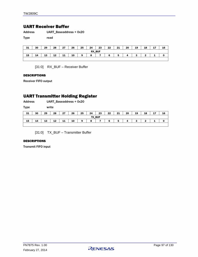
TW2809C
FN7875 Rev. 1.00 Page 97 of 130
February 27, 2014
UART Receiver Buffer Address UART_Baseaddress + 0x20
Type read
31 30 29 28 27 26 25 24 23 22 21 20 19 18 17 16
RX_BUF
15 14 13 12 11 10 9 8 7 6 5 4 3 2 1 0
[31:0] RX_BUF – Receiver Buffer
DESCRIPTIONS
Receiver FIFO output
UART Transmitter Holding Register Address UART_Baseaddress + 0x20
Type write
31 30 29 28 27 26 25 24 23 22 21 20 19 18 17 16
TX_BUF
15 14 13 12 11 10 9 8 7 6 5 4 3 2 1 0
[31:0] TX_BUF – Transmitter Buffer
DESCRIPTIONS
Transmit FIFO input

TW2809C
FN7875 Rev. 1.00 Page 98 of 130
February 27, 2014
GPIO Register Definitions
GPIO Interrupt Enable Register Address GPIO_Baseaddress + 0x00
Type write
31 30 29 28 27 26 25 24 23 22 21 20 19 18 17 16
GPIO
interrupt
status
clear
15 14 13 12 11 10 9 8 7 6 5 4 3 2 1 0
GPIO
interrupt
enable
[16] GPIO Interrupt Status Clear- FW can clear GPIO interrupt by writing HIGH to this bit.
[00] GPIO Interrupt Enable - GPIO Interrupt can be enabled by writing HIGH to this bit.
DESCRIPTIONS
GPIO Interrupt Status clear bit can clear the interrupt status bit by writing bit 16 “1”.

TW2809C
FN7875 Rev. 1.00 Page 99 of 130
February 27, 2014
GPIO Interrupt Status Register Address GPIO_Baseaddress + 0x00
Type read
31 30 29 28 27 26 25 24 23 22 21 20 19 18 17 16
15 14 13 12 11 10 9 8 7 6 5 4 3 2 1 0
GPIO
interrupt
status
[00] GPIO Interrupt Status- GPIO set this bit to HIGH to interrupt FW.
DESCRIPTIONS
GPIO Line Driving Register0 Address GPIO_Baseaddress + 0x30
Type write
31 30 29 28 27 26 25 24 23 22 21 20 19 18 17 16
GPIO Line Driver 31:24 GPIO Line Driver 23:16
15 14 13 12 11 10 9 8 7 6 5 4 3 2 1 0
GPIO Line Driver 15:8 GPIO Line Driver 7:0
[31: 24] GPIO Line Driver 31:24 – Output Data from GPIO 31 to 24
[23: 16] GPIO Line Driver 23:16 – Output Data from GPIO 23 to 16
[15: 8] GPIO Line Driver 15:8 – Output Data from GPIO 15 to 8
[7: 0] GPIO Line Driver 7:0 – Output Data from GPIO 7 to 0
DESCRIPTIONS
GPIO Line Driver 31 : 0

TW2809C
FN7875 Rev. 1.00 Page 100 of 130
February 27, 2014
GPIO Line Driving Register1
Address GPIO_Baseaddress + 0x34
Type write
31 30 29 28 27 26 25 24 23 22 21 20 19 18 17 16
GPIO Line Driver 55:48
15 14 13 12 11 10 9 8 7 6 5 4 3 2 1 0
GPIO Line Driver 47:40 GPIO Line Driver 39:32
[23: 16] GPIO Line Driver 55:48 – Output Data from GPIO 55 to 48
[15: 8] GPIO Line Driver 47:40 –Output Data from GPIO 47 to 40
[7: 0] GPIO Line Driver 39:32 –Output Data from GPIO 39 to 32
DESCRIPTIONS
GPIO Line Driver 55 : 32
GPIO Line Control Register0 Address GPIO_Baseaddress + 0x40
Type write
31 30 29 28 27 26 25 24 23 22 21 20 19 18 17 16
GPIO Direction Control 31:24 GPIO Direction Control 23:16
15 14 13 12 11 10 9 8 7 6 5 4 3 2 1 0
GPIO Direction Control 15:8 GPIO Direction Control 7:0
[31:24] GPIO Direction Control 31:24 – Input and Output Pin Direction Control from GPIO 31 to 24
1 : Output, 0: Input
[23:16] GPIO Direction Control 23:16 – Input and Output Pin Direction Control from GPIO 23 to 16
1 : Output, 0: Input
[15:8] GPIO Direction Control 15:8 – Input and Output Pin Direction Control from GPIO 15 to 8
1 : Output, 0: Input
[7:0] GPIO Direction Control 7:0 – Input and Output Pin Direction Control from GPIO 7 to 0
1 : Output, 0: Input
DESCRIPTIONS
GPIO Line Control Register0 : Input/Output Control 31 : 0

TW2809C
FN7875 Rev. 1.00 Page 101 of 130
February 27, 2014
GPIO Line Control Register1
Address GPIO_Baseaddress + 0x44
Type write
31 30 29 28 27 26 25 24 23 22 21 20 19 18 17 16
GPIO Direction Control 55:48
15 14 13 12 11 10 9 8 7 6 5 4 3 2 1 0
GPIO Direction Control 47:40 GPIO Direction Control 39:32
[23: 16] GPIO Direction Control 55:48 – Input and Output Pin Direction Control from GPIO 55 to 48
1 : Output, 0: Input
[15: 8] GPIO Direction Control 47:40 –Input and Output Pin Direction Control from GPIO 47 to 40
1 : Output, 0: Input
[7: 0] GPIO Direction Control 39:32 –Input and Output Pin Direction Control from GPIO 39 to 32
1 : Output, 0: Input
DESCRIPTIONS
GPIO Line Control Register1 : Input/Output Control 55 : 32
GPIO Line Load Register0 Address GPIO_Baseaddress + 0x20
Type read
31 30 29 28 27 26 25 24 23 22 21 20 19 18 17 16
GPIO Line Load 31:24 GPIO Line Load 23:16
15 14 13 12 11 10 9 8 7 6 5 4 3 2 1 0
GPIO Line Load 15:8 GPIO Line Load 7:0
[31: 24] GPIO Line Load 31:24 –Input Pin from GPIO 31 to 24
[23: 16] GPIO Line Load 23:16 –Input Pin from GPIO 23 to 16
[15: 8] GPIO Line Load 15:8 –Input Pin from GPIO 15 to 8
[7: 0] GPIO Line Load 7:0 –Input Pin from GPIO 7 to 0
DESCRIPTIONS
GPIO Line Load 31 : 0

TW2809C
FN7875 Rev. 1.00 Page 102 of 130
February 27, 2014
GPIO Line Load Register1
Address GPIO_Baseaddress + 0x24
Type read
31 30 29 28 27 26 25 24 23 22 21 20 19 18 17 16
GPIO Line Load 55:48
15 14 13 12 11 10 9 8 7 6 5 4 3 2 1 0
GPIO Line Load 47:40 GPIO Line Load 39:32
[23: 16] GPIO Line Load 55:48 – Input Data from GPIO 55 to 48
[15: 8] GPIO Line Load 47:40 –Input Data from GPIO 47 to 40
[7: 0] GPIO Line Load 39:32 –Input Data from GPIO 39 to 32
DESCRIPTIONS
GPIO Line Load 55 : 32
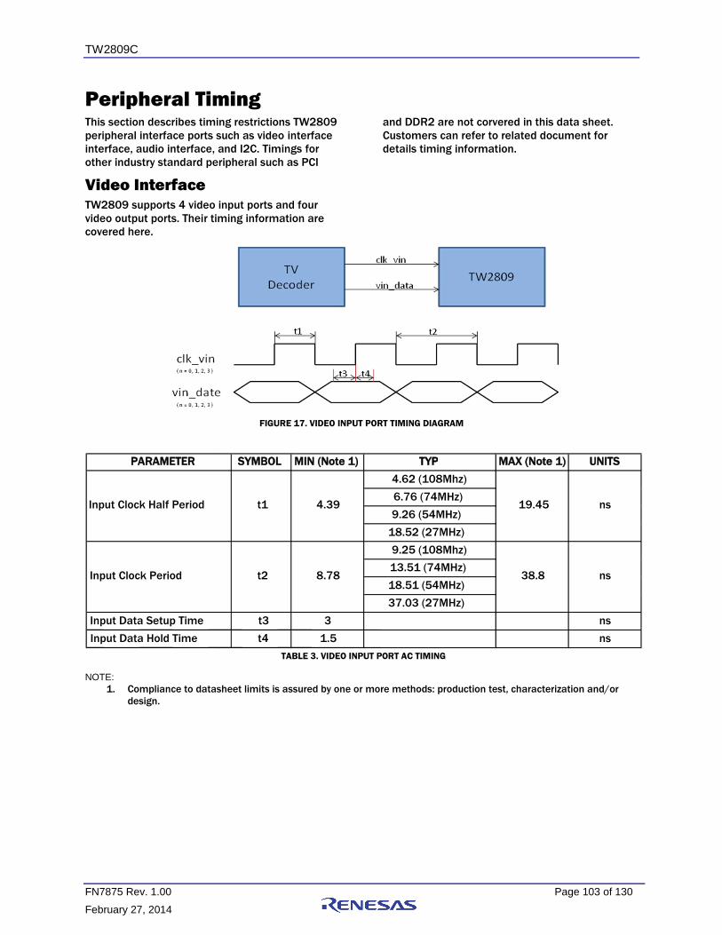
TW2809C
FN7875 Rev. 1.00 Page 103 of 130
February 27, 2014
Peripheral Timing
This section describes timing restrictions TW2809
peripheral interface ports such as video interface
interface, audio interface, and I2C. Timings for
other industry standard peripheral such as PCI
and DDR2 are not corvered in this data sheet.
Customers can refer to related document for
details timing information.
Video Interface TW2809 supports 4 video input ports and four
video output ports. Their timing information are
covered here.
FIGURE 17. VIDEO INPUT PORT TIMING DIAGRAM
NOTE:
1. Compliance to datasheet limits is assured by one or more methods: production test, characterization and/or
design.
PARAMETER SYMBOL MIN (Note 1) TYP MAX (Note 1) UNITS
4.62 (108Mhz)
6.76 (74MHz)
9.26 (54MHz)
18.52 (27MHz)
9.25 (108Mhz)
13.51 (74MHz)
18.51 (54MHz)
37.03 (27MHz)
Input Data Setup Time t3 3 ns
Input Data Hold Time t4 1.5 ns
Input Clock Period t2 8.78 38.8 ns
Input Clock Half Period t1 4.39 19.45 ns
TABLE 3. VIDEO INPUT PORT AC TIMING

TW2809C
FN7875 Rev. 1.00 Page 104 of 130
February 27, 2014
FIGURE 18. VIDEO OUTPUT PORT TIMING DIAGRAM
PARAMETER SYMBOL MIN (NOTE1) TYP MAX (NOTE1) UNITS
OUTPUT CLOCK HALF PERIOD t1 4.39
4.62 (108MHz)
19.45 ns 6.76 (74MHz)
9.26 (54MHz)
18.52 (27MHz)
OUTPUT CLOCK PERIOD t2 8.78
9.25 ( 108MHz)
38.8 ns 13.51 (74MHz)
18.51 (54MHz)
37.03 (27MHz)
OUTPUT DATA DELAY t3 2.6
5.2 ns
TABLE 4. VIDEO OUTPUT PORT AC TIMING
NOTE:
1. Compliance to datasheet limits is assured by one or more methods: production test, characterization and/or
design.

TW2809C
FN7875 Rev. 1.00 Page 105 of 130
February 27, 2014
Audio Interface This section describs audio interface port timing.
TW2809 audio interfaces follows industry
standard I2S protocal with modifications to
support multi-channel audio.
FIGURE 19. AUDIO INPUT PORT TIMING DIAGRAM
FIGURE 20-1. AUDIO OUTPUT PORT TIMING DIAGRAM
PARAMETER SYMBOL MIN TYP MAX UNITS
ASYNR,ADATR,ADATM propagation delay TA_pd 0.6 2 ns
ACLKP High pulse duration TA_hw 37 ns
ACLKP Low pulse duration TA_lw 74 ns
ASYNP, ADATP setup time TA_su 36 ns
ASYNP, ADATP hold time TA_h 35 ns
TABLE 5. AUDIO INPUT PORT AC TIMING
NOTE:
1. TA_lw Min value and TA_su Min value are Fs=48KHz mode only. If Fs < 48KHz, these Min values are
more bigger. High period of ACLKR/ACLKP is 27Mhz one clock period.

TW2809C
FN7875 Rev. 1.00 Page 106 of 130
February 27, 2014
I2C Interface This section describs I2C interface timing for
TW2809.
FIGURE 21. I2C PORT TIMING DIAGRAM
TABLE 6. I2C INPUT PORT AC TIMING
NOTE:
1. Compliance to datasheet limits is assured by one or more methods: production test, characterization and/or
design.
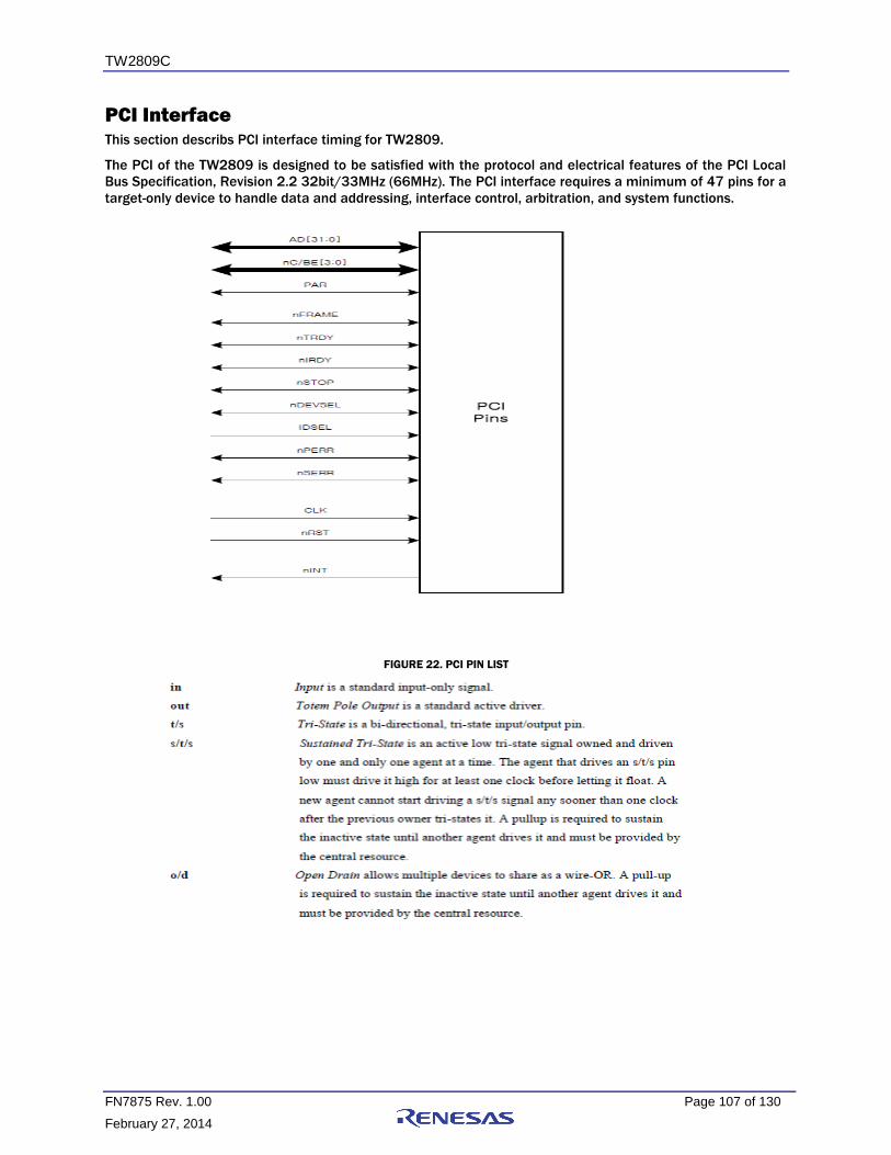
TW2809C
FN7875 Rev. 1.00 Page 107 of 130
February 27, 2014
PCI Interface
This section describs PCI interface timing for TW2809.
The PCI of the TW2809 is designed to be satisfied with the protocol and electrical features of the PCI Local
Bus Specification, Revision 2.2 32bit/33MHz (66MHz). The PCI interface requires a minimum of 47 pins for a
target-only device to handle data and addressing, interface control, arbitration, and system functions.
FIGURE 22. PCI PIN LIST

TW2809C
FN7875 Rev. 1.00 Page 108 of 130
February 27, 2014
SYSTEM PINS
CLK
in
Clock provides timing for all transactions on PCI and is an input to every PCI device. All other
PCI signals, except nRST, and nINTD, are sampled on the rising edge of CLK and all other
timing parameters are defined with respect to this edge. PCI operates up to 33 MHz and, in
general, the minimum frequency is DC (0 Hz).
nRST in Reset is used to bring PCI-specific registers, sequencers, and signals to a consistent state.
What effect nRST has on a device beyond the PCI sequencer is beyond the scope of this
specification, except for reset states of required PCI configuration registers. A device that can
wake the system while in a powered down bus state has additional requirements related to
nRST. Refer to the PCI Power Management Interface Specification for details. Anytime nRST is
asserted, all PCI output signals must be driven to their benign state. In general, this means
they must be asynchronously tri-stated. nREQ and nGNT must both be tristated (they cannot be
driven low or high during reset). To prevent AD, nC/BE, and PAR signals from floating during
reset, the central resource may drive these lines during reset (bus parking) but only to a logic
low level; they may not be driven high.
nRST may be asynchronous to CLK when asserted or deasserted. Although asynchronous,
deassertion is guaranteed to be a clean, bounce-free edge. Except for configuration accesses,
only devices that are required to boot the system will respond after reset.
ADDRESS AND DATA PINS
AD[31:0] t/s Address and Data are multiplexed on the same PCI pins. A bus transaction consists of an
address2 phase followed by one or more data phases. PCI supports both read and write bursts.
The address phase is the first clock cycle in which nFRAME is asserted. During the address
phase, AD[31:0] contain a physical address (32 bits). For I/O, this is a byte address; for
configuration and memory, it is a DWORD address. During data phases, AD[07:0] contain the
least significant byte (lsb) and AD[31:24] contain the most significant byte (msb). Write data is
stable and valid when nIRDY is asserted; read data is stable and valid when nTRDY is asserted.
Data is transferred during those clocks where both nIRDY and nTRDY are asserted.
nC/BE[3:0] t/s Bus Command and Byte Enables are multiplexed on the same PCI pins. During the address
phase of a transaction, nC/BE[3:0] define the bus command. During the data phase,
nC/BE[3:0] are used as Byte Enables. The Byte Enables are valid for the entire data phase and
determine which byte lanes carry meaningful data. nC/BE[0] applies to byte 0 (lsb) and
nC/BE[3] applies to byte 3 (msb).
PAR t/s Parity is even3 parity across AD[31:0] and nC/BE[3:0]. Parity generation is required by all PCI
agents. PAR is stable and valid one clock after each address phase. For data phases, PAR is
stable and valid one clock after either nIRDY is asserted on a write transaction or nTRDY is
asserted on a read transaction. Once PAR is valid, it remains valid until one clock after the
completion of the current data phase. (PAR has the same timing as AD[31:0], but it is delayed
by one clock.) The master drives PAR for address and write data phases; the target drives PAR
for read data phases.
INTERFACE CONTROL PINS
nFRAME s/t/s Cycle Frame is driven by the current master to indicate the beginning and duration of an
access. nFRAME is asserted to indicate a bus transaction is beginning. While nFRAME is
asserted, data transfers continue. When nFRAME is deasserted, the transaction is in the final
data phase or has completed.
nIRDY s/t/s Cycle Frame is driven by the current master to indicate the beginning and duration of an
access. nFRAME is asserted to indicate a bus transaction is beginning. While nFRAME is
asserted, data transfers continue. When nFRAME is deasserted, the transaction is in the final
data phase or has completed.
nTRDY s/t/s Target Ready indicates the target agent’s (selected device’s) ability to complete the current
data phase of the transaction. nTRDY is used in conjunction with nIRDY. A data phase is
completed on any clock both nTRDY and nIRDY are asserted. During a read, nTRDY indicates
that valid data is present on AD[31:0]. During a write, it indicates the target is prepared to
accept data. Wait cycles are inserted until both nIRDY and nTRDY are asserted together.
nSTOP s/t/s Stop indicates the current target is requesting the master to stop the current transaction.

TW2809C
FN7875 Rev. 1.00 Page 109 of 130
February 27, 2014
nLOCK s/t/s Lock indicates an atomic operation to a bridge that may require multiple transactions to
complete. When nLOCK is asserted, non-exclusive transactions may proceed to a bridge that is
not currently locked. A grant to start a transaction on PCI does not guarantee control of nLOCK.
Control of nLOCK is obtained under its own protocol in conjunction with nGNT. It is possible for
different agents to use PCI while a single master retains ownership of nLOCK. Locked
transactions may be initiated only by host bridges, PCI-to- PCI bridges, and expansion bus
bridges. Refer to Appendix F for details on the requirements of nLOCK..
IDSEL in Initialization Device Select is used as a chip select during configuration read and write
transactions.
nDEVSEL s/t/s Device Select, when actively driven, indicates the driving device has decoded its address as the
target of the current access. As an input, nDEVSEL indicates whether any device on the bus has
been selected.
ARBITRATION PINS (BUS MASTERS ONLY)
nREQ t/s Request indicates to the arbiter that this agent desires use of the bus. This is a point-to-point
signal. Every master has its own nREQ which must be tri-stated while nRST is asserted.
nGNT t/s Grant indicates to the agent that access to the bus has been granted. This is a point-to-point
signal. Every master has its own nGNT which must be ignored while nRST is asserted.
ERROR REPORTING PINS
nPERR s/t/s Parity Error is only for the reporting of data parity errors during all PCI transactions except a
Special Cycle. The nPERR pin is sustained tri-state and must be driven active by the agent
receiving data (when enabled) two clocks following the data when a data parity error is
detected. The minimum duration of nPERR is one clock for each data phase that a data parity
error is detected. (If sequential data phases each have a data parity error, the nPERR signal
will be asserted for more than a single clock.) nPERR must be driven high for one clock before
being tri-stated as with all sustained tri-state signals.
nSERR o/d System Error is for reporting address parity errors, data parity errors on the Special Cycle
command, or any other system error where the result will be catastrophic. If an agent does not
want a non-maskable interrupt (NMI) to be generated, a different reporting mechanism is
required. nSERR is pure open drain and is actively driven for a single PCI clock by the agent
reporting the error. The assertion of nSERR is synchronous to the clock and meets the setup
and hold times of all bused signals. However, the restoring of nSERR to the deasserted state is
accomplished by a weak pullup (same value as used for s/t/s) which is provided by the central
resource not by the signaling agent. This pullup may take two to three clock periods to fully
restore nSERR. The agent that reports nSERR to the operating system does so anytime nSERR
is asserted.
INTERRUPT PINS (OPTIONAL)
nINT o/d Interrupt is used to request an interrupt.
Exactly how the IDSEL pin is driven is left to the discretion of the host/memory bridge or system designer.
This signal has been designed to allow its connection to one of the upper 21 address lines, which are not
otherwise used in a configuration access. However, there is no specified way of determining IDSEL from the
upper 21 address bits. Therefore, the IDSEL pin must be supported by all targets. Devices must not make an
internal connection between an AD line and an internal IDSEL signal in order to save a pin. The only exception
is the host bridge, since it defines how IDSELs are mapped. IDSEL generation behind a PCI-to-PCI bridge is
specified in the PCI-to-PCI Bridge Architecture Specification. How a system generates IDSEL is system
specific; however, if no other mapping is required, the following example may be used. The IDSEL signal
associated with Device Number 0 is connected to AD[16], IDSEL of Device Number 1 is connected to AD[17],
and so forth until IDSEL of Device Number 15 is connected to AD[31]. For Device Number 17-31, the host
bridge should execute the transaction but not assert any of the AD[31:16] lines but allow the access to be
terminated with Master-Abort.
Twenty-one different devices can be uniquely selected for configuration accesses by connecting a different
address line to each device an asserting one of the AD[31:11] lines at a time. The issue with connecting one
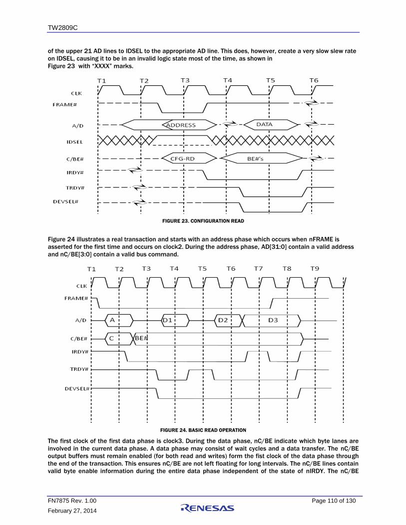
TW2809C
FN7875 Rev. 1.00 Page 110 of 130
February 27, 2014
of the upper 21 AD lines to IDSEL to the appropriate AD line. This does, however, create a very slow slew rate
on IDSEL, causing it to be in an invalid logic state most of the time, as shown in
Figure 23 with “XXXX” marks.
FIGURE 23. CONFIGURATION READ
Figure 24 illustrates a real transaction and starts with an address phase which occurs when nFRAME is
asserted for the first time and occurs on clock2. During the address phase, AD[31:0] contain a valid address
and nC/BE[3:0] contain a valid bus command.
FIGURE 24. BASIC READ OPERATION
The first clock of the first data phase is clock3. During the data phase, nC/BE indicate which byte lanes are
involved in the current data phase. A data phase may consist of wait cycles and a data transfer. The nC/BE
output buffers must remain enabled (for both read and writes) form the fist clock of the data phase through
the end of the transaction. This ensures nC/BE are not left floating for long intervals. The nC/BE lines contain
valid byte enable information during the entire data phase independent of the state of nIRDY. The nC/BE

TW2809C
FN7875 Rev. 1.00 Page 111 of 130
February 27, 2014
lines contain the byte enable information for data phase N+1 on the clock following the completion of the
data phase N. This is not shown in Figure 24 because a burst read transaction typically has all byte enables
asserted; however, it is shown in Figure 25. Notice on clock 5 in Figure 25, the master inserted a wait state
by deasserting nIRDY. However, the byte enables for data phase 3 are valid on clock 5 and remain valid until
the data phase completes on clock 8.
The fist data phase on a read transaction requires a turnaround-cycle (enforced by the target via nTRDY). In
this case, the address is valid on clock2 and then the master stops driving AD. The earliest the target can
provide valid data is clock 4. The target must drive the AD lines following the turnaround cycle when nDEVSEL
is asserted. Once enabled, the output buffers must stay enabled through the end of the transaction. (This
ensures that the AD lines are not left floating for lone intervals.)
One way for a data phase to complete is when data is transferred, which occurs when both nIRDY and nTRDY
are asserted on the same rising clock edge. There are other conditions that complete a data phase. (nTRDY
cannot be driven until nDEVSEL is asserted.) When either nIRDY or nTRDY is deasseted, a wait cycle is
inserted and no data is transferred. Data is successfully transferred on clocks 4, 6, and 8 and wait cycles are
inserted on clock 3, 5, and 7. The first data phase completes in the minimum time for a read transaction. The
second data phase is extended on clock 5 because nTRDY is deasserted. The last data phase is extended
because nIRDY was deasserted on clock 7.
The master knows at clock 7 that the next data phase is the last. However, because the master is not ready
to complete the last transfer (nIRDY is deasserted on clock 7), nFRAME stays asserted. Only when nIRDY is
asserted can nFRAME be deasserted as occurs on clock 8, indicating to the target that this is the last data
phase of the transaction.
Figure 25 illustrates a write transaction. The transaction starts when nFRAME is asserted for the first time
which occurs on clock 2. A write transaction is similar to a read transaction except no turnaround cycle is
required following the address phase because the master provides both address and data. Data phases work
the same for both read and write transactions.
FIGURE 25. BASIC WRITE OPERATION
In Figure 25, the first and second data phases complete with zero wait cycles. However, the third data phase
has three wait cycles inserted by the target. Notice both agents insert a wait cycle on clock 5. nIRDY must be
asserted when nFRAME is deasserted indicating the last data phase.

TW2809C
FN7875 Rev. 1.00 Page 112 of 130
February 27, 2014
The date transfer was delayed by the master on clock 5 because nIRDY was deasserted. The last data phase
is signaled by the master on clock 6, but it does not complete until clock 8.
Table 7 shows PCI configuration registers, which is listed up initial values. Device ID, Vendor ID, Subsys ID,
Subsys Vendor ID, Class Code, Rev ID, Header Type, Max Lat, Min Gnt and Int Pin of PCI configuration
registers can be update by only PCI configuration EEPROM. Command, Status, Latency Timer, Cache Line
Size, Memory Base Address, Interrupt Line, Retry Timeout and TRDY Timeout of PCI configuration registers
can be update by PCI configuration write as shown as Figure 23. In this case, PCI command needs to be
change as PCI configuration write instead of PCI configuration read. In addition, PCI configuration read is
used to read PCI configuration registers for checking initial value and updated value.
TABLE 7. PCI CONFIGURATION REGISTERS
31 16 15 0 Offset Initial Value
Device ID Vendor ID 00h 2809_1797h
Status Command 04h 02a0_0007h
Class Code Revision ID 08h 048000_02h
BIST Header Type Latency Timer Cache line Size 0Ch 00_00_00_00h
Memory Base Address 10h 00_00000_8h(?)
Reserved 14h
Reserved 18h
Reserved 1Ch
Reserved 20h
Reserved 24h
Card bus CIS Pointer 28h 0000_0000h
Subsystem ID Subsystem Vendor ID 2Ch 2809_1719h
Expansion ROM Base Address 30h 0000_0000h
Reserved Capabilities
Pointers 34h 000000_00h
Reserved 38h
Max_Lat Min_Gnt Interrupt Pin Interrupt Line 3Ch 48_20_01_00h
Reserved Retry Timeout TRDY Timeout 40h 0000_80_80h
TABLE 8. CONTENTS OF PCI CONFIGURATION EEPROM
Address Contents
00h Vendor ID
04h Device ID
58h Subsystem Vendor ID
5Ch Subsystem ID
78h Interrupt Pin
7Ch Max_Lat Min_Gnt

TW2809C
FN7875 Rev. 1.00 Page 113 of 130
February 27, 2014
UART Interface The UART serial communication parameters comply with EIA-RS-232-C Interface Standard. The frame
properties are specified in Figure 26. Every frame starts with the start bit (which is always 0), followed by the
least significant data bit (indicated with D0). Then the next data bits are succeeding, ending with the most
significant bit (indicated with D7).
FIGURE 26. FRAME STRUCTURE (ST=START BIT, DN=DATA BITS, P=PARITBIT, SP=STOP BIT)
The parity bit is inserted after the data bits, before the stop bit (which is always 1). When a complete frame is
transmitted, it can be directly followed by a new frame, or the communication line can be set to an idle (high)
state. Each frame corresponds to a single byte of information.
Each command or query can consist of one or several successive RxD frames. The lamp driver will answer
accordingly with one or several successive TxD frames. Figure 27 shows the communication flow and defines
the timing limit for receiving and transmitting TMAX Command and TMAX Response.
Following timing limits in the communication flow have to be kept:
if after the time TMAX Command = 15 ms a whole command is not transmitted completely to the
lamp driver, the command queue is cleared (this is necessary to synchronize the command
decoding algorithm with the projector electronics) and the error byte ABh is returned;
the response will start earliest after having received the first frame of a command and latest after
having received the last frame of a command plus a processing time, which can vary between zero
and 5 ms. The whole response time is guaranteed to be finished after TMAX Response = 10 ms.
FIGURE 27. COMMUNICATION FLOW CHART
TABLE 9. UART PARAMETER
Frame Parameter Value Tolerance
Baud Rate 128000 (max.) ±1%
Number of Start Bits 1 n/a
Number of Data Bits 8 n/a
Number of Stop Bits 1/2 n/a
Parity Bit Odd/Even/None n/a
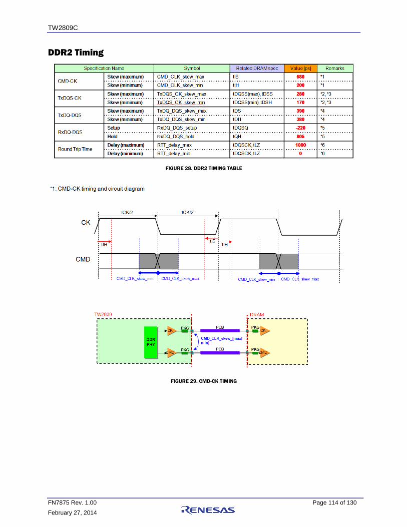
TW2809C
FN7875 Rev. 1.00 Page 114 of 130
February 27, 2014
DDR2 Timing
FIGURE 28. DDR2 TIMING TABLE
FIGURE 29. CMD-CK TIMING

TW2809C
FN7875 Rev. 1.00 Page 115 of 130
February 27, 2014
FIGURE 30. TXDQS-CK TIMNG FOR TDQSS
FIGURE 31. TXDQS-CK TIMING FOR TDSS/TDSH

TW2809C
FN7875 Rev. 1.00 Page 116 of 130
February 27, 2014
FIGURE 32. TXDQ-DQS TIMING
FIGURE 33. RXDQ-DQS TIMING

TW2809C
FN7875 Rev. 1.00 Page 117 of 130
February 27, 2014
FIGURE 34. ROUND TRIP PATH TIMING

TW2809C
FN7875 Rev. 1.00 Page 118 of 130
February 27, 2014
Power Up Sequence The TW2809 has to follow certain power up sequence to guarantee working. It shows in the diagram below.
1.8V DDR I/O
Power Supply
3.3V I/O
Power Supply
hw_rst_n
ref_clk
Regulator Power up
time to chip power
stable time delay
Don’t care
Min. 740us
1.8V DDR I/O
Power Supply
1.2V Core
Power Supply0us( Min. )
Internal Clock s
PLL lock time ( 240 us )
PLL reset time
: 5us( Min. )740us + t_cfg + 245 us = 985us + t_cfg us
1.2V Core
Power SupplyDon’t care
3.3V I/O
Power Supply
1.8V DDR I/O
Power Supply0us( Min. )
pci_config_done
Config time (t_cfg us )
pci_rst_in_n
pci_rst_in_n
hw_rst_n0us( Min. )
FIGURE 35. TW2809 POWER UP SEQUENCE
Power Off Sequence The TW2809 has to follow certain power off sequence to guarantee working. It shows in the diagram below.
Figure 36. TW2809 POWER OFF SEQUENCE
document or the summary of an
interesting point. You can position
the text box anywhere in the
document. Use the Text Box Tools
tab to change the formatting of the
pull quote text box.]

TW2809C
FN7875 Rev. 1.00 Page 119 of 130
February 27, 2014
Electrical Specifications
ABSOLUTE MAXIMUM RATINGS
PARAMETER SYMBOL MIN TYP MAX UNITS
Vref DVDI -0.5 1.2 1.8 V
PLL AVD AVDD -0.5 1.2 1.8 V
DDR AVD 1.8V SSTL_VDE -0.5 1.8 2.5 V
VDD 3.3V DVDE -0.5 3.3 4.6 V
Voltage on Any Digital Data Pin
(See Caution statement) - -0.5 - 3.8 V
Voltage on OSC Related Analog Pin - -0.5 - 3.8 V
Storage Temperature TS -55 - 125 °C
Junction Temperature TJ -40 - 125 °C
Reflow Soldering ( ≤ 10 Seconds) TPEAK - - 240 - 250 °C
CAUTION: Do not operate at or near the maximum ratings listed for extended periods of time. Exposure to such conditions may adversely impact product reliability and result in failures not covered by warranty.
RECOMMENDED OPERATING CONDITIONS
PARAMETER SYMBOL MIN TYP MAX UNITS
Vref DVDI 1.10 1.2 1.25 V
PLL AVD AVDD 1.15 1.2 1.25 V
DDR AVD SSTL_VDE 1.7 1.8 1.9 V
VDD 3.3V DVDE 3.0 3.3 3.6 V
Ambient Operating Temperature TA 0 25 70 °C
SUPPLY CURRENT AND POWER DISSIPATION
PARAMETER SYMBOL MIN TYP MAX UNITS
PLL Supply Current (1.2V nom) IDDP 18.2 mA
SSTL 1.8V Supply Current (1.8V nom) IDDH 215 mA
Digital Internal Supply Current (1.2V nom) IDDI 580 mA
Digital I/O Supply Current (3.3V nom) IDDO 18.87 mA
Total Power Dissipation Pd 1.16 W

TW2809C
FN7875 Rev. 1.00 Page 120 of 130
February 27, 2014
DC CHARACTERISTICS
PARAMETER SYMBOL MIN
(NOTE 1) TYP
MAX
(NOTE 1) UNITS
Digital Inputs
Input High Voltage (TTL) VIH 2.0 --- VDDE + 0.3 V
Input Low Voltage (TTL) VIL 0.3 --- 0.8 V
Input Leakage Current
(@VI = 3.3V or 0V) IL --- --- ± 4 µA
Input Capacitance CIN --- --- 16 pF
Digital Outputs
Output High Voltage VOH VDDE 0.2 --- VDDE V
Output Low Voltage VOL 0 --- 0.2 V
High Level Output Current
(@VOH = 2.8V) IOH
*1
mA
Low Level Output Current
(@VOL = 0.2V) IOL mA
Tri-state Output Leakage Current
(@VO = 2.5V or 0V) IOZ --- --- ± 4 µA
Output Capacitance CO --- --- 16 pF
INPUT / OUTPUT CAPACITANCE
PARAMETER SYMBOL REQUIREMENTS UNITS
Input Pin CIN Max 16 pF
Output Pin COUT Max 16 pF
I/O Pin CI/O Max 16 pF
NOTES:
1. Compliance to datasheet limits is assured by one or more methods: production test, characterization and/or
design.
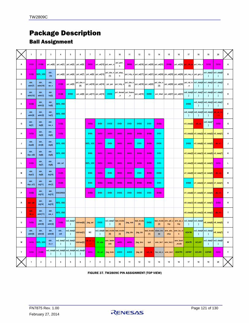
TW2809C
FN7875 Rev. 1.00 Page 121 of 130
February 27, 2014
Package Description
Ball Assignment
1 2 3 4 5 6 7 8 9 10 11 12 13 14 15 16 17 18 19 20
A DVSS DVSS pci_ad[0] pci_ad[1] pci_ad[3] pci_ad[6] DVSS pci_ad[12] pci_serr_npci_perr_
nDVSS pci_ad[16] pci_ad[20] pci_ad[23] DVSS pci_ad[28] pci_clk_in pci_inta_n DVSS DVSS A
B DVSS SSTL_VDEddr_
ckepci_ad[2] pci_ad[4] pci_ad[7] pci_ad[9] pci_ad[13]
pci_cbe_n
[1]
pci_stop_
npci_irdy_n pci_ad[17] pci_ad[21] pci_ad[24] pic_ad[25] pci_ad[29] pci_req_n pci_gnt_n
vo1_data[1
]
vo1_data[0
]B
Cddr_
addr[7]
ddr_
addr[10]
ddr_
we_nDVSS pci_ad[5]
pci_cbe_n
[0]pci_ad[10] pci_ad[14] pci_par pci_trdy_n
pci_cbe_n
[2]pci_ad[18] pci_ad[22]
pci_cbe_n
[3]pci_ad[26] pci_ad[30]
pci_rst_in
_n
vo1_data[4
]
vo1_data[3
]
vo1_data[2
]C
Dddr_
addr[12]
ddr_
addr[1]
ddr_
ba[2]DVSS DVDE pci_ad[8] pci_ad[11] pci_ad[15] DVDE
pci_devsel
_n
pci_frame
_npci_ad[19] DVDE pci_idsel pci_ad[27] pci_ad[31]
vo0_data[0
]
vo1_data[7
]
vo1_data[6
]
vo1_data[5
]D
E DVSSddr_
addr[3]
ddr_
ba[0]SSTL_VDE DVDE
vo0_data[3
]
vo0_data[2
]
vo0_data[1
]E
Fddr_
addr[9]
ddr_
addr[5]
ddr_
ba[1]SSTL_VDE
vo0_data[6
]
vo0_data[5
]
vo0_data[4
]
clk_vo_ou
t_0F
Gddr_
dq[1]
ddr_
dq[0]
ddr_
ras_nDVSS DVSS DVDI DVDE DVDI DVDI DVDE DVDI DVSS vi3_data[0] clk_vo
vo0_data[7
]DVSS G
H DVSSddr_
dq[3]
ddr_
dq[2]DVSS DVDI DVSS DVSS DVSS DVSS DVSS DVSS DVDI vi3_data[4] vi3_data[3] vi3_data[2] vi3_data[1] H
Jddr_
dqs[0]
ddr_
dm[0]
ddr_
dq[4]SSTL_VDE SSTL_VDE DVSS DVDI DVSS DVSS DVDI DVSS DVDE DVDE vi3_data[6] vi3_data[5] clk_vi3 J
Kddr_
dqs_n[0]
ddr_
dq[6]
ddr_
dq[5]SSTL_VDE DVDI DVSS DVSS DVSS DVSS DVSS DVSS DVDI vi2_data[2] vi2_data[1] vi2_data[0] vi3_data[7] K
L DVSSddr_
dq[7]
ddr_
dq[8]ddr_ref SSTL_VDE DVSS DVSS DVSS DVSS DVSS DVSS DVDI vi2_data[5] vi2_data[4] vi2_data[3] DVSS L
Mddr_
dqs[1]
ddr_
dq[9]
ddr_
dq[10]DVSS DVDI DVSS DVDI DVSS DVSS DVDI DVSS DVDE vi1_data[0] vi2_data[7] vi2_data[6] clk_vi2 M
Nddr_
dqs_n[1]
ddr_
dq[11]
ddr_
dm[1]DVSS DVDI DVSS DVSS DVSS DVSS DVSS DVSS DVDI DVDE vi1_data[3] vi1_data[2] vi1_data[1] N
P DVSSddr_
dq[12]
ddr_
dq[13]DOCDRES DVSS DVDI DVDI DVDE DVDI DVDE DVDI DVSS vi1_data[6] vi1_data[5] vi1_data[4] clk_vi1 P
R ddr_clkddr_
dq[14]
ddr_
dq[15]SSTL_VDE vi0_data[1] vi0_data[0] vi1_data[7] DVSS R
Tddr_
clk_n
ddr_
addr[11]
ddr_
cas_nSSTL_VDE vi0_data[4] vi0_data[3] vi0_data[2] clk_vi0 T
U DVSSddr_
addr[6]
ddr_
addr[2]DVSS
vo2_data[1
]iddrtest[0] jtag_sel DVDE
vo3_data[7
]
test_mode
[4]jtag_rtck
test_mode
[0]DVDE
test_mode
[2]
arm_sdi_c
hip
arm_se_c
hip
vo3_data[3
]
vo3_data[5
]vi0_data[6] vi0_data[5] U
Vddr_
addr[8]
ddr_
addr[4]
ddr_
addr[0]
ddr_
odt
vo2_data[2
]iddrtest[1] NC
vo3_data[6
]
test_mode
[5]
test_mode
[3]jtag_tdo jtag_tck
test_mode
[1]
slave_mo
de
arm_sdo_
chip
arm_bu_cl
kADATM
vo3_data[4
]
vo3_data[2
]vi0_data[7] V
W DVSS SSTL_VDEddr_
cs_n
vo2_data[7
]
vo2_data[3
]iddrtest[2]
clk_vo_ou
t_1i2c_sda
arm_testm
odeAVSS AVSS jtag_tms vpd arm_tm1 arm_trst_t
arm_boot
_modeADATR ACLKP
vo3_data[1
]
vo3_data[0
]W
Y DVSS DVSSvo2_data[6
]
vo2_data[5
]
vo2_data[4
]
vo2_data[0
]DVSS i2c_scl jtag_trstn AVDD AVDD jtag_tdi ref_clk hw_rst_n arm_tm2 ADATP0 ASYNP ACLKR ASYNR DVSS Y
1 2 3 4 5 6 7 8 9 10 11 12 13 14 15 16 17 18 19 20
FIGURE 37. TW2809C PIN ASSIGNMENT (TOP VIEW)

TW2809C
FN7875 Rev. 1.00 Page 122 of 130
February 27, 2014
Pin Definitions
TABLE 10. PIN DEFINITIONS
BALL NO. SYMBOL ATTRIBUTE DESCRIPTIONS
Y13 ref_clk Input Chip reference clock input (54MHz)
Y14 hw_rst_n Input Chip reset input (active low)
V14 slave_mode Input TW2809C operation mode (Tied to “1”)
R1 ddr_clk Output DDR differential clocks
T1 ddr_clk_n
V3 ddr_addr[0] Output DDR address bus
D2 ddr_addr[1]
U3 ddr_addr[2]
E2 ddr_addr[3]
V2 ddr_addr[4]
F2 ddr_addr[5]
U2 ddr_addr[6]
C1 ddr_addr[7]
V1 ddr_addr[8]
F1 ddr_addr[9]
C2 ddr_addr[10]
T2 ddr_addr[11]
D1 ddr_addr[12]
E3 ddr_ba[0] Output DDR control signals
F3 ddr_ba[1]
D3 ddr_ba[2]
B3 ddr_cke
W3 ddr_cs_n
G3 ddr_ras_n
T3 ddr_cas_n
C3 ddr_we_n
V4 ddr_odt
G2 ddr_dq[0] I/O DDR data bus
G1 ddr_dq[1]
H3 ddr_dq[2]
H2 ddr_dq[3]
J3 ddr_dq[4]

TW2809C
FN7875 Rev. 1.00 Page 123 of 130
February 27, 2014
BALL NO. SYMBOL ATTRIBUTE DESCRIPTIONS
K3 ddr_dq[5]
K2 ddr_dq[6]
L2 ddr_dq[7]
L3 ddr_dq[8]
M2 ddr_dq[9]
M3 ddr_dq[10]
N2 ddr_dq[11]
P2 ddr_dq[12]
P3 ddr_dq[13]
R2 ddr_dq[14]
R3 ddr_dq[15]
J1 ddr_dqs[0] I/O DDR differential data strobe
K1 ddr_dqs_n[0]
M1 ddr_dqs[1]
N1 ddr_dqs_n[1]
J2 ddr_dm[0] Output DDR data write mask
N3 ddr_dm[1]
P4 DOCDRES Output DDR SSTL_18 special purpose output signal
(1.8v)
L4 ddr_ref Input DDR SSTL_18 reference voltage (1.8v)
A17 pci_clk_in Input PCI input clock (33/66 MHz)
A3 pci_ad[0] I/O PCI address and data bus
A4 pci_ad[1]
B4 pci_ad[2]
A5 pci_ad[3]
B5 pci_ad[4]
C5 pci_ad[5]
A6 pci_ad[6]
B6 pci_ad[7]
D6 pci_ad[8]
B7 pci_ad[9]
C7 pci_ad[10]
D7 pci_ad[11]
A8 pci_ad[12]
B8 pci_ad[13]

TW2809C
FN7875 Rev. 1.00 Page 124 of 130
February 27, 2014
BALL NO. SYMBOL ATTRIBUTE DESCRIPTIONS
C8 pci_ad[14]
D8 pci_ad[15]
A12 pci_ad[16]
B12 pci_ad[17]
C12 pci_ad[18]
D12 pci_ad[19]
A13 pci_ad[20]
B13 pci_ad[21]
C13 pci_ad[22]
A14 pci_ad[23]
B14 pci_ad[24]
B15 pci_ad[25]
C15 pci_ad[26]
D15 pci_ad[27]
A16 pci_ad[28]
B16 pci_ad[29]
C16 pci_ad[30]
D16 pci_ad[31]
C6 pci_cbe_n[0] I/O PCI bus command and byte enable
B9 pci_cbe_n[1]
C11 pci_cbe_n[2]
C14 pci_cbe_n[3]
C17 pci_rst_in_n Input PCI control signals
C9 pci_par I/O
D11 pci_frame_n I/O
B11 pci_irdy_n I/O
C10 pci_trdy_n I/O
B10 pci_stop_n I/O
D14 pci_idsel Input
D10 pci_devsel_n I/O
B17 pci_req_n I/O
B18 pci_gnt_n Input
A10 pci_perr_n I/O
A9 pci_serr_n I/O

TW2809C
FN7875 Rev. 1.00 Page 125 of 130
February 27, 2014
BALL NO. SYMBOL ATTRIBUTE DESCRIPTIONS
A18 pci_inta_n Output
G18 clk_vo Input VO clock input to generate internal four
video output ports clocks
F20 clk_vo_out_0 Output VO clock output for video output ports 0 and
1
D17 vo0_data[0] I/O VO video output port 0 data buas
E20 vo0_data[1]
E19 vo0_data[2] Note: vo0_data[7:0] is pin muxed with
GPIO[23:16]
E18 vo0_data[3]
F19 vo0_data[4]
F18 vo0_data[5]
F17 vo0_data[6]
G19 vo0_data[7]
B20 vo1_data[0] I/O VO video output port 1 data buas
B19 vo1_data[1]
C20 vo1_data[2] Note1: vo1_data[7:0] is pin muxed with
GPIO[15:8]
C19 vo1_data[3]
C18 vo1_data[4]
D20 vo1_data[5]
D19 vo1_data[6]
D18 vo1_data[7]
W7 clk_vo_out_1 Output VO clock output for video output ports 2 and
3
Y6 vo2_data[0] I/O VO video output port 2 data buas
U5 vo2_data[1]
V5 vo2_data[2] Note: vo2_data[7:0] is pin muxed with
GPIO[7:0]
W5 vo2_data[3]
Y5 vo2_data[4]
Y4 vo2_data[5]
Y3 vo2_data[6]
W4 vo2_data[7]
W20 vo3_data[0] I/O VO video output port 3 data buas
W19 vo3_data[1]
V19 vo3_data[2] Note1: vo3_data[7:0] is pin muxed with

TW2809C
FN7875 Rev. 1.00 Page 126 of 130
February 27, 2014
BALL NO. SYMBOL ATTRIBUTE DESCRIPTIONS
U17 vo3_data[3] GPIO[55:48]
V18 vo3_data[4]
U18 vo3_data[5]
V8 vo3_data[6]
U9 vo3_data[7]
T20 clk_vi0 Input VI video input port 0 clock input
R18 vi0_data[0] Input VI video input port 0 data bus
R17 vi0_data[1]
T19 vi0_data[2]
T18 vi0_data[3]
T17 vi0_data[4]
U20 vi0_data[5]
U19 vi0_data[6]
V20 vi0_data[7]
P20 clk_vi1 Input VI video input port 1 clock input
M17 vi1_data[0] I/O VI video input port 2 data bus
N20 vi1_data[1]
N19 vi1_data[2] Note: vi1_data[7:0] is pin muxed with
GPIO[47:40]
N18 vi1_data[3]
P19 vi1_data[4]
P18 vi1_data[5]
P17 vi1_data[6]
R19 vi1_data[7]
M20 clk_vi2 Input VI video input port 2 clock input
K19 vi2_data[0] I/O VI video input port 2 data bus
K18 vi2_data[1]
K17 vi2_data[2] Note: vi2_data[7:0] is pin muxed with
GPIO[39:32]
L19 vi2_data[3]
L18 vi2_data[4]
L17 vi2_data[5]
M19 vi2_data[6]
M18 vi2_data[7]
J20 clk_vi3 Input VI video input port 3 clock input

TW2809C
FN7875 Rev. 1.00 Page 127 of 130
February 27, 2014
BALL NO. SYMBOL ATTRIBUTE DESCRIPTIONS
G17 vi3_data[0] I/O VI video input port 3 data bus
H20 vi3_data[1]
H19 vi3_data[2] Note1: vi3_data[7:0] is pin muxed with
GPIO[31:24]
H18 vi3_data[3] Note2: vi3_data[0] is pin muxed with
UART0_Rx
H17 vi3_data[4] Note3: vi3_data[1] is pin muxed with
UART0_Tx
J19 vi3_data[5] Note4: vi3_data[2] is pin muxed with
UART1_Rx
J18 vi3_data[6] Note5: vi3_data[3] is pin muxed with
UART1_Tx
K20 vi3_data[7]
W18 ACLKP I/O AUDIO playback port bit clock, word select,
and serial data Y17 ASYNP
Y16 ADATP0
Y18 ACLKR Input AUDIO record port bit clock, word select,
and serial data Y19 ASYNR
W17 ADATR
V17 ADATM Input PLL test pin (Tied to ground "0")
V7 NC Not connected
W16 arm_boot_mode Input ARM926 IP test pins ( Tied to ground “0”)
W9 arm_tstmode
W14 arm_tm1
Y15 arm_tm2
W15 arm_trst_t
V16 arm_bu_clk
U16 arm_se_chip
U15 arm_sdi_chip
V15 arm_sdo_chip Output
W13 vpd Input All DDR Phy IP test pins (Tied to ground “0”)
U6 iddrtest[0]
V6 iddrtest[1]
W6 iddrtest[2]
U12 test_mode[0] Input All Global test mode pins (Tied to ground
“0”) V13 test_mode[1]

TW2809C
FN7875 Rev. 1.00 Page 128 of 130
February 27, 2014
BALL NO. SYMBOL ATTRIBUTE DESCRIPTIONS
U14 test_mode[2]
V10 test_mode[3]
U10 test_mode[4]
V9 test_mode[5]
V12 jtag_tck Input JTAG test pins. All 5 input pins should be
tied to LOW for normal operation. Y9 jtag_trstn Input
Y12 jtag_tdi Input
U7 jtag_sel Input
W12 jtag_tms Input
V11 jtag_tdo Output
U11 jtag_rtck Output
Y8 i2c_scl I/O I2C interface
W8 i2c_sda I/O
Y10,Y11 AVDD 1.2V Power of analog PLL
W10,W11 AVSS - Ground of analog PLL
G8,G10,G11,G13,H7,
H14,J9,J12,K7,K14,
L14,M7,M9,M12,N7,
N14,P8,P9,P11,P13
DVDI 1.2V Power of core logic
B2,E4,F4,J4,J7,
K4,L7,R4,T4,W2
SSTL_VDE 1.8V Power of the DDR I/O
D5,D9,D13,E17,G9,
G12,J14,J17,M14,
N17,P10,P12,U8,U13
DVDE 3.3V Power of the external I/O
A1,A2,A7,A11,A15,
A19,A20,B1,C4,D4,
E1,G4,G7,G14,G20,
H1,H4,H8,H9,H10,
H11,H12,H13,J8,
J10,J11,J13,K8,K9,
K10,K11,K12,K13,
DVSS - Ground
TW2809C
FN7875 Rev. 1.00 Page 129 of 130
February 27, 2014
BALL NO. SYMBOL ATTRIBUTE DESCRIPTIONS
L1,L8,L9,L10,L11,
L12,L13,L20,M4,
M8,M10,M11,M13,
N4,N8,N9,N10,N11,
N12,N13,P1,P7,P14,
R20,U1,U4,W1,Y1,
Y2,Y7,Y20
DVSS
About
Intersil
Intersil Corporation is a leading provider of innovative power management and precision analog solutions.
The company's products address some of the largest markets within the industrial and infrastructure, mobile
computing and high-end consumer markets.
For the most updated datasheet, application notes, related documentation and related parts, please see the
respective product information page found at www.intersil.com.
You may report errors or suggestions for improving this datasheet by visiting www.intersil.com/ask.
Reliability reports are also available from our website at www.intersil.com/support
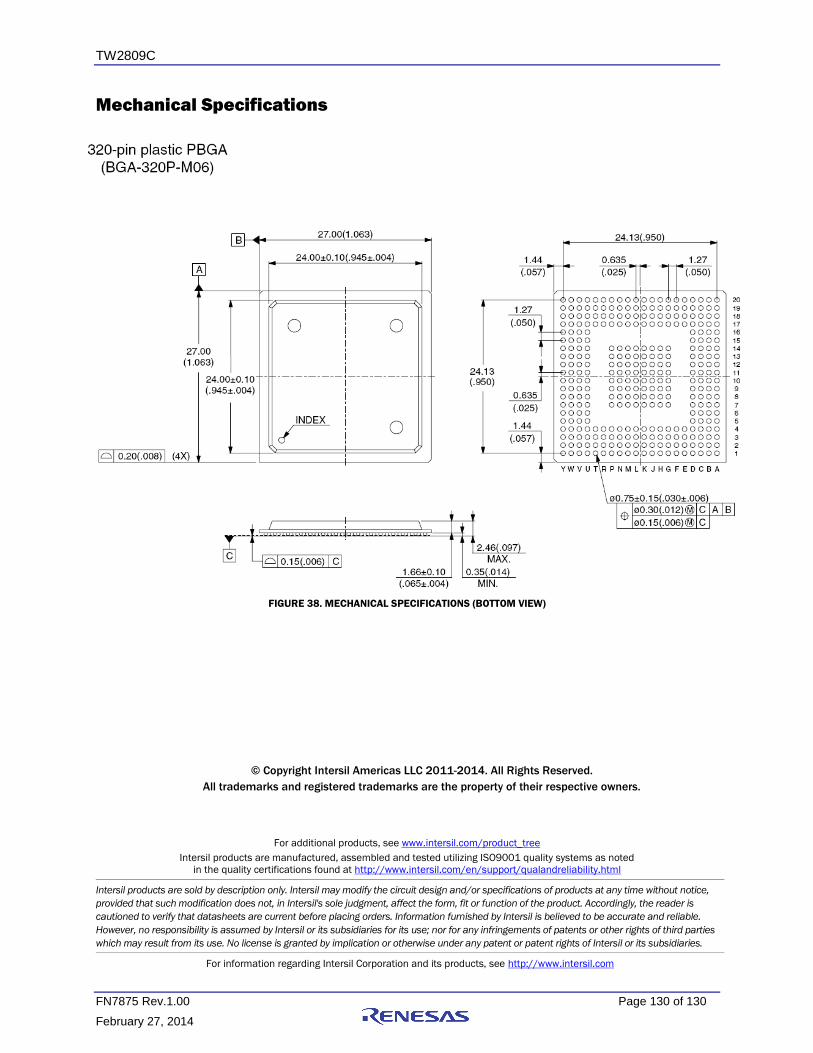
TW2809C
For additional products, see www.intersil.com/product_tree
Intersil products are manufactured, assembled and tested utilizing ISO9001 quality systems as noted
in the quality certifications found at http://www.intersil.com/en/support/qualandreliability.html
Intersil products are sold by description only. Intersil may modify the circuit design and/or specifications of products at any time without notice,
provided that such modification does not, in Intersil's sole judgment, affect the form, fit or function of the product. Accordingly, the reader is
cautioned to verify that datasheets are current before placing orders. Information furnished by Intersil is believed to be accurate and reliable.
However, no responsibility is assumed by Intersil or its subsidiaries for its use; nor for any infringements of patents or other rights of third parties
which may result from its use. No license is granted by implication or otherwise under any patent or patent rights of Intersil or its subsidiaries.
For information regarding Intersil Corporation and its products, see http://www.intersil.com
FN7875 Rev.1.00 Page 130 of 130
February 27, 2014
Mechanical Specifications
FIGURE 38. MECHANICAL SPECIFICATIONS (BOTTOM VIEW)
© Copyright Intersil Americas LLC 2011-2014. All Rights Reserved.
All trademarks and registered trademarks are the property of their respective owners.
Recommended