Embed Size (px)
DESCRIPTION
ZigBee network
Citation preview

ZigBee for wireless networking
Johan Lönn
Jonas Olsson
15th March 2005

Preface
This report is the result of a Master Thesis work done at Linköping University. Thediploma work was done at the Department of Science and Technology (ITN), inNorrköping.
The authors would like to thank Professor Shaofang Gong, Pär Håkansson andAndreas Kingbäck at ITN for useful discussions and suggestions during the project.
Special thanks to all the people from Chipcon, Atmel, NDK, gigaAnt and ACTE forsupplying devices, and also for the technical support.
I

Abstract
The past several years have witnessed a rapid development in the wireless network area.So far wireless networking has been focused on high-speed and long range applications.However, there are many wireless monitoring and control applications for industrialand home environments which require longer battery life, lower data rates and lesscomplexity than those from existing standards. What the market need is a globallydened standard that meets the requirement for reliability, security, low power and lowcost. For such wireless applications a new standard called ZigBee has been developedby the ZigBee Alliance based upon the IEEE 802.15.4 standard.
The aim of this diploma work is to design fully functional ZigBee and IEEE 802.15.4modules, and to evaluate an application in a sensor network.
This diploma work has resulted in two fully functional ZigBee and IEEE 802.15.4modules, respectively. It is also shown that ZigBee sensors can be networked wirelessly.
Eventually it is the authors hope that the modules will be used within ITN, and alsobe developed further for new applications.
II

Sammanfattning
De senaste åren har det skett en mycket snabb utveckling inom området trådlösa nätverk.Hittills har fokus legat på snabba överföringar och lång räckvidd. Dock nns det ettotal applikationer inom t ex. industrin för övervakning och kontroll, vilka kräver län-gre batteritid, lägre överföringshastighet och framförallt mindre komplexitet än dagensstandarder. Det som dessa marknader behöver är en global standard som nogranntfyller kraven på säkerhet, tillförlitlighet, låg eektförbrukning och låg kostnad. Fördessa typer av applikationer har en ny standard utvecklats av ZigBee Alliance, vilkenbaseras på standarden IEEE 802.15.4.
Målet med detta examensarbete är att designa och tillverka fullt fungerande trådlösaZigBee och IEEE 802.15.4 moduler, samt att utvärdera en applikation i ett sensornätverk.
Examensarbetet har resulterat i två olika fullt fungerande ZigBee och IEEE 802.15.4moduler. Rapporten beskriver också att det är möjligt att ansluta olika typer av sensorertill ett ZigBee nätverk.
Slutligen är det författarnas förhoppningar att modulerna kommer att användas inomITN, samt även utvecklas ytterligare för nya applikationer.
III

Contents
Terminology X
1 Introduction 11.1 Background . . . . . . . . . . . . . . . . . . . . . . . . . . . . . . . . . . 11.2 Goal . . . . . . . . . . . . . . . . . . . . . . . . . . . . . . . . . . . . . . 11.3 Method . . . . . . . . . . . . . . . . . . . . . . . . . . . . . . . . . . . . 21.4 Outline . . . . . . . . . . . . . . . . . . . . . . . . . . . . . . . . . . . . . 2
2 Theory 32.1 ZigBee Alliance . . . . . . . . . . . . . . . . . . . . . . . . . . . . . . . . 32.2 The name ZigBee . . . . . . . . . . . . . . . . . . . . . . . . . . . . . . . 42.3 IEEE 802.15.4 . . . . . . . . . . . . . . . . . . . . . . . . . . . . . . . . . 4
2.3.1 Components of the IEEE 802.15.4 . . . . . . . . . . . . . . . . . . 42.3.2 Network topologies . . . . . . . . . . . . . . . . . . . . . . . . . . 52.3.3 OSI Overview . . . . . . . . . . . . . . . . . . . . . . . . . . . . . 62.3.4 Physical Layer . . . . . . . . . . . . . . . . . . . . . . . . . . . . . 62.3.5 Medium Access Control Layer . . . . . . . . . . . . . . . . . . . . 11
2.4 Hardware . . . . . . . . . . . . . . . . . . . . . . . . . . . . . . . . . . . 122.5 Security . . . . . . . . . . . . . . . . . . . . . . . . . . . . . . . . . . . . 12
2.5.1 Unsecured mode . . . . . . . . . . . . . . . . . . . . . . . . . . . 122.5.2 Access control list . . . . . . . . . . . . . . . . . . . . . . . . . . . 122.5.3 Secured mode . . . . . . . . . . . . . . . . . . . . . . . . . . . . . 12
2.6 ZigBee Stack . . . . . . . . . . . . . . . . . . . . . . . . . . . . . . . . . 132.7 ZigBee Networking . . . . . . . . . . . . . . . . . . . . . . . . . . . . . . 14
3 Design Process 153.1 Design Description . . . . . . . . . . . . . . . . . . . . . . . . . . . . . . 153.2 Components . . . . . . . . . . . . . . . . . . . . . . . . . . . . . . . . . . 15
3.2.1 Microcontroller Unit . . . . . . . . . . . . . . . . . . . . . . . . . 153.2.2 RF Transceiver/Microcontroller Conguration and Data Interface 183.2.3 RF Circuit . . . . . . . . . . . . . . . . . . . . . . . . . . . . . . . 183.2.4 Connector . . . . . . . . . . . . . . . . . . . . . . . . . . . . . . . 213.2.5 Power Supply . . . . . . . . . . . . . . . . . . . . . . . . . . . . . 21
3.3 Printed Circuit Board Layout . . . . . . . . . . . . . . . . . . . . . . . . 213.3.1 PCB Overview . . . . . . . . . . . . . . . . . . . . . . . . . . . . 213.3.2 General Layout Guidelines . . . . . . . . . . . . . . . . . . . . . . 22
IV

3.3.3 BalUn Layout . . . . . . . . . . . . . . . . . . . . . . . . . . . . . 233.3.4 GND Vias . . . . . . . . . . . . . . . . . . . . . . . . . . . . . . . 23
4 Implementation 254.1 PCB Manufacturing . . . . . . . . . . . . . . . . . . . . . . . . . . . . . 254.2 Assembly . . . . . . . . . . . . . . . . . . . . . . . . . . . . . . . . . . . 264.3 Soldering . . . . . . . . . . . . . . . . . . . . . . . . . . . . . . . . . . . . 264.4 Bill Of Material . . . . . . . . . . . . . . . . . . . . . . . . . . . . . . . . 264.5 Assembled Modules . . . . . . . . . . . . . . . . . . . . . . . . . . . . . . 26
5 Development Tools 295.1 CC2420 ZigBee DK Development Kit . . . . . . . . . . . . . . . . . . . . 295.2 ATmega128L Tools . . . . . . . . . . . . . . . . . . . . . . . . . . . . . . 30
5.2.1 AVR GCC Tool . . . . . . . . . . . . . . . . . . . . . . . . . . . . 305.2.2 Atmel AVR Studio . . . . . . . . . . . . . . . . . . . . . . . . . . 305.2.3 Programmer's Notepad . . . . . . . . . . . . . . . . . . . . . . . . 31
5.3 PCB Tool . . . . . . . . . . . . . . . . . . . . . . . . . . . . . . . . . . . 32
6 Test Application 336.1 Temperature Coordinator . . . . . . . . . . . . . . . . . . . . . . . . . . 346.2 Temperature Sensor . . . . . . . . . . . . . . . . . . . . . . . . . . . . . . 35
7 Results 36
8 Discussions 37
9 Conclusions 38
10 Further work 39
Bibliography 40
A Tools 42
B PCB Layout 43
C Schematics 48
D Bill of Material 52
E Datasheets 56
V

List of Figures
2.1 Network topologies . . . . . . . . . . . . . . . . . . . . . . . . . . . . . . 52.2 OSI model . . . . . . . . . . . . . . . . . . . . . . . . . . . . . . . . . . . 62.3 Modulation and spreading . . . . . . . . . . . . . . . . . . . . . . . . . . 72.4 Error vector . . . . . . . . . . . . . . . . . . . . . . . . . . . . . . . . . . 92.5 Mesh network . . . . . . . . . . . . . . . . . . . . . . . . . . . . . . . . . 14
3.1 RF+MCU module block diagram . . . . . . . . . . . . . . . . . . . . . . 163.2 MCU circuit . . . . . . . . . . . . . . . . . . . . . . . . . . . . . . . . . . 173.3 RF circuit . . . . . . . . . . . . . . . . . . . . . . . . . . . . . . . . . . . 203.4 RF+MCU module . . . . . . . . . . . . . . . . . . . . . . . . . . . . . . 223.5 RF module . . . . . . . . . . . . . . . . . . . . . . . . . . . . . . . . . . 223.6 Layer stackup . . . . . . . . . . . . . . . . . . . . . . . . . . . . . . . . . 223.7 BalUn layout . . . . . . . . . . . . . . . . . . . . . . . . . . . . . . . . . 233.8 Ground vias (bottom view) . . . . . . . . . . . . . . . . . . . . . . . . . 24
5.1 CC2420 ZigBee DK Development Kit . . . . . . . . . . . . . . . . . . . . 295.2 AVR studio . . . . . . . . . . . . . . . . . . . . . . . . . . . . . . . . . . 305.3 Programmer's Notepad . . . . . . . . . . . . . . . . . . . . . . . . . . . . 315.4 Protel DXP 2004 layout environment . . . . . . . . . . . . . . . . . . . . 32
6.1 Temperature coordinator . . . . . . . . . . . . . . . . . . . . . . . . . . . 346.2 Temperature coordinator ow . . . . . . . . . . . . . . . . . . . . . . . . 346.3 Temperature sensor ow . . . . . . . . . . . . . . . . . . . . . . . . . . . 356.4 Temperature sensor ow . . . . . . . . . . . . . . . . . . . . . . . . . . . 35
A.1 Smith Chart tool in ADS . . . . . . . . . . . . . . . . . . . . . . . . . . . 42
B.1 RF+MCU module top layer . . . . . . . . . . . . . . . . . . . . . . . . . 43B.2 RF+MCU module power/GND plane, negative . . . . . . . . . . . . . . 44B.3 RF+MCU module GND plane, negative . . . . . . . . . . . . . . . . . . 44B.4 RF+MCU module bottom layer . . . . . . . . . . . . . . . . . . . . . . . 45B.5 RF module top layer . . . . . . . . . . . . . . . . . . . . . . . . . . . . . 45B.6 RF module power/GND plane, negative . . . . . . . . . . . . . . . . . . 46B.7 RF module GND plane, negative . . . . . . . . . . . . . . . . . . . . . . 46B.8 RF module bottom layer . . . . . . . . . . . . . . . . . . . . . . . . . . . 47
C.1 Schematic of RF+MCU module . . . . . . . . . . . . . . . . . . . . . . . 49C.2 Schematic of RF module . . . . . . . . . . . . . . . . . . . . . . . . . . . 50
VI

C.3 Schematic of JTAG connector . . . . . . . . . . . . . . . . . . . . . . . . 51
D.1 The BOM for the RF+MCU module . . . . . . . . . . . . . . . . . . . . 53D.2 The BOM for the RF+MCU module . . . . . . . . . . . . . . . . . . . . 54D.3 The BOM for the RF module . . . . . . . . . . . . . . . . . . . . . . . . 55
E.1 Datasheet for the RF+MCU module . . . . . . . . . . . . . . . . . . . . 57E.2 Datasheet for the RF module . . . . . . . . . . . . . . . . . . . . . . . . 58
VII

List of Tables
2.1 Frequency bands and data rates . . . . . . . . . . . . . . . . . . . . . . . 72.2 Channels and how to calculate them . . . . . . . . . . . . . . . . . . . . 72.3 Symbol to chip mapping . . . . . . . . . . . . . . . . . . . . . . . . . . . 82.4 2.4GHz transceivers . . . . . . . . . . . . . . . . . . . . . . . . . . . . . . 122.5 ZigBee stack . . . . . . . . . . . . . . . . . . . . . . . . . . . . . . . . . . 13
3.1 Atmel ATmega128L JTAG interface . . . . . . . . . . . . . . . . . . . . 163.2 RF Transceiver/Microcontroller interface . . . . . . . . . . . . . . . . . . 19
4.1 PCB dimensions for RF+MCU module . . . . . . . . . . . . . . . . . . . 264.2 RF+MCU module pin list . . . . . . . . . . . . . . . . . . . . . . . . . . 274.3 RF module pin list . . . . . . . . . . . . . . . . . . . . . . . . . . . . . . 28
VIII

Terminology
Abbreviation Explanation
ADS Advanced Design System.
BalUn Balanced to Unbalanced
BOM Bill Of Material
CCA Clear Channel Assessment
CTS Clear To Send
dBm decibel-milliwatt
ED Energy Detection
ESR Equivalent Series Resistans
EVM Error-Vector Magnitude
FFD Full Function Device
GPIO General Purpose Input/Output
GTS Guaranteed Time Slot
IEEE Institute of Electrical and Electronics Engineers
I In-phase carrier
ISP In-System Programmer
LOS Line Of Sight
LQI Link Quality Indication
MAC Medium Access Control
MIC Message Integrity Code
MSK Minimum Shift Keying
MN Matching Network
OQPSK Oset Quadrature Phase-Shift Keying
PA Power Amplier
PAN Personal Area Network
IX

Abbreviation Explanation
PCB Printed Circuit Board
PER Packet Error Rate
PPDU PHY Protocol Data Unit
PHY Physical Layer
Q Quadrature-phase carrier
RF Radio Frequency
RFD Reduced-Function Device
RTC Real Time Clock
RTS Ready To Send
RX Receiver
SMD Surfaced Mounted Device
TX Transmitter
WLAN Wireless Local Area Network
X

Chapter 1
Introduction
The past several years have witnessed a rapid growth of wireless networking. However,up to now wireless networking has been mainly focused on high-speed communications,and relatively long range applications such as the IEEE 802.11 Wireless Local AreaNetwork (WLAN) standards. The rst well known standard focusing on Low-RateWireless Personal Area Networks (LR-WPAN) was Bluetooth. However it has limitedcapacity for networking of many nodes. There are many wireless monitoring and controlapplications in industrial and home environments which require longer battery life, lowerdata rates and less complexity than those from existing standards. For such wirelessapplications, a new standard called IEEE 802.15.4 has been developed by IEEE. Thenew standard is also called ZigBee, when additional stack layers dened by the ZigBeeAlliance are used.
1.1 Background
This project has been performed as a diploma work for a Master of Science degree inElectrical Engineering at Linköping University. The project has been done at ITN,Campus Norrköping. The Communication Electronics research group, lead by professorShaofang Gong, has a big interest in new wireless standards and applications. Since thereis no standard covering the wireless sensor networking, it is of interest to investigate andevaluate this new standard. One of the questions are how to handle a large number ofwireless sensors in the same network. Another interesting task is how to optimize thebattery life time of a wireless sensor.
1.2 Goal
The goal of this project is to develop fully functional wireless ZigBee and IEEE 802.15.4modules. This includes design using Protel DXP 2004, and implementation of the ZigBeeprotocol stack. To evaluate the new standard, a literature study must be performed. Atest application will also be developed, in order to test the functionality of the ZigBeemodules.
1

1.3. METHOD CHAPTER 1. INTRODUCTION
1.3 Method
The work is divided into several dierent sections. Firstly, a literature study is per-formed. Secondly, to be able to test the ZigBee and IEEE 802.15.4 standards a lab-oration kit is purchased. Thirdly, Protel DXP 2004 is used for design of the ZigBeemodules. The modules are then manufactured outside the university, but the assemblyis preformed in-house. After the hardware development, implementation of the softwarestack is performed. Finally a test application is developed.
The information to the project is obtained mainly from the Internet, but also fromspecic literatures.
1.4 Outline
The report is divided into several sections, and a brief overview of the sections aredescribed here.
• Chapter 2 - Theory. This is a description of the ZigBee and IEEE 802.15.4 stan-dards.
• Chapter 3 - Design Process. The design process and the dierent parts of thesystem are described.
• Chapter 4 - Implementation. The implementation of the modules are described.
• Chapter 5 - Development Tools. The software and hardware required to run anddevelop the modules are described.
• Chapter 6 - Test Application. The developed test application is described.
• Chapter 7 - Results. The results of the project is presented here.
• Chapter 8 - Discussions. Discussions regarding the results obtained from thisproject are presented.
• Chapter 9 - Conclusions. Conclusions drawn from the project.
• Chapter 10 - Further work. Further work to be done in the area.
2

Chapter 2
Theory
This chapter briey describes some of the technology background that has been used inthis thesis work.
2.1 ZigBee Alliance
The ZigBee Alliance is an association of companies working together to dene an openglobal standard for making low-power wireless networks. The intended outcome ofZigBee Alliance is to create a specication dening how to build dierent network topolo-gies with data security features and interoperable application proles. The associationincludes companies from a wide spectrum of categories, from chip manufactures to sys-tem integration companies. The number of members in the association is rapidly growingand is currently over 125 (Q1 2005). Among the members one can nd Philips, Samsung,Motorola and LG.
The rst specication was ratied in Q4 2004 and the rst generation of ZigBeeproducts may reach the market sometime in 2005. A big challenge for the alliance is tomake the interoperability to work among dierent products. To solve this problem, theZigBee Alliance has dened dierent proles, depending on what type of category theproduct belongs to. For example there is an prole called Home Lightning that exactlydenes how dierent brands of home lightning-products should communicate with eachother.
To get access to the specication one must currently (Q1 2005) become a memberof the ZigBee Alliance, but it will become public later in this year (2005).
Currently there are three dierent types of ZigBee proles:
• Private proleInteroperability NOT important. No ZigBee stamp on the product, but one canclaim "based on a ZigBee platform"
• Published proleA private prole is shared with others. No ZigBee stamp on the product, but onecan claim "based on a ZigBee platform"
• Public proleThe ocial ZigBee prole.
3

2.2. THE NAME ZIGBEE CHAPTER 2. THEORY
2.2 The name ZigBee
The name ZigBee is said to come from the domestic honeybee which uses a zig-zagtype of dance to communicate important information to other hive members. Thiscommunication dance (the "ZigBee Principle") is what engineers are trying to emulatewith this protocol a bunch of separate and simple organisms that join together totackle complex tasks.
2.3 IEEE 802.15.4
The goal IEEE had when they specied the IEEE 802.15.4 standard was to provide astandard for ultra-low complexity, ultra-low cost, ultra-low power consumption and lowdata rate wireless connectivity among inexpensive devices. The raw data rate will behigh enough (maximum of 250 kb/s) for applications like sensors, alarms and toys.
2.3.1 Components of the IEEE 802.15.4
IEEE 802.15.4 networks use three types of devices:
• The network Coordinator maintains overall network knowledge. It is the mostsophisticated one of the three types, and requires the most memory and computingpower.
• The Full Function Device (FFD) supports all IEEE 802.15.4 functions and featuresspecied by the standard. It can function as a network coordinator. Additionalmemory and computing power make it ideal for network router functions or itcould be used in network-edge devices (where the network touches the real world).
• The Reduced Function Device (RFD) carries limited (as specied by the standard)functionality to lower cost and complexity. It is generally found in network-edgedevices. The RFD can be used where extremely low power consumption is anecessity.
4

2.3. IEEE 802.15.4 CHAPTER 2. THEORY
2.3.2 Network topologies
IEEE 802.15.4 can manage two types of networks, i.e., star topology or the peer-to-peer topology. Both the topologies are illustrated in Figure 2.1. In ZigBee, these twotopologies can be combined to build so-called mesh networks.
Figure 2.1: Network topologies
Star network formation
The rst FFD that is activated may establish its own network and become a PersonalArea Network (PAN) coordinator. Then both FFD and RFD devices can connect to thePAN coordinator. All networks within the radio sphere of inuence must have a uniquePAN identity. All nodes in a PAN must talk to the PAN Coordinator.
Peer-to-Peer network formation
In the peer-to-peer topology there is also a PAN coordinator, but it diers from the startopology in that any device can communicate with any other device as long as they arein the range of one another. The peer-to-peer topology allows more complex networkformations to be implemented, such as the mesh topology.
5

2.3. IEEE 802.15.4 CHAPTER 2. THEORY
2.3.3 OSI Overview
The Open System Interconnection (OSI) reference model, was developed by the Inter-national Organization for Standardization (ISO) as a model for the computer protocolarchitecture, and as a framework for developing protocol standards. The entire pointof the model is to separate networking into several distinct functions that operate atdierent levels. Each layer is responsible for performing a specic task or set of tasks,and dealing with the layers above and below it. An illustration of the general OSI-modeland where ZigBee is dened in the model can be seen in Figure 2.2.
Figure 2.2: OSI model
2.3.4 Physical Layer
The IEEE 802.15.4 specication denes three dierent frequency bands, in order toconform with regulations in Europe, Japan, Canada and the United States. Table 2.1
6

2.3. IEEE 802.15.4 CHAPTER 2. THEORY
describes the frequency bands and data rates. Totally 27 channels are available acrossthe dierent frequency bands, as described in Table 2.2.
Table 2.1: Frequency bands and data ratesPHY Frequency band Chip rate Modulation Bit rate Symbol rate Symbols
(MHz) (MHz) (kchips/s) (kb/s) (ksymbol/s)
868 868-868.6 300 BPSK 20 20 Binary
915 902-928 600 BPSK 40 40 Binary
2450 2400-2483.5 2000 O-QPSK 250 62.5 16-ary
Orthogonal
Table 2.2: Channels and how to calculate themCenter frequency Number of channels Channel Channel center frequency
(MHz) (N) (k) (MHz)
868 1 0 868.3
915 10 1 - 10 906+2(k-1)
2450 16 11 - 26 2405+5(k-11)
Modulation/Spreading
The conversion of the binary data to a modulated signal in the 2450 MHz frequencyband can be described as the functional block diagram in Figure 2.3. The numbersshow how the binary data "0000b" is converted to a baseband chip sequence with pulseshaping.
Figure 2.3: Modulation and spreading
Bit to symbol
The rst step is to encode all the data in the PHY Protocol Data Unit (PPDU) frombinary data to symbols. Each byte is divided into two symbols and the least signicant
7

2.3. IEEE 802.15.4 CHAPTER 2. THEORY
symbol is transmitted rst. For multi-byte elds, the least signicant byte is transmittedrst, except for security related elds where the most signicant byte is transmitted rst.
Symbol to chip
Each data symbol is mapped into a Pseudo-random (PN) 32-chip sequence. The chipsequence is then transmitted at 2 MChip/s with the least signicant chip (c0) trans-mitted rst for each symbol. Table 2.3 shows the data symbol with corresponding chipvalues.
Table 2.3: Symbol to chip mappingData symbol Chip values
(decimal) (c0 c1... c30c31 )
0 1 1 0 1 1 0 0 1 1 1 0 0 0 0 1 1 0 1 0 1 0 0 1 0 0 0 1 0 1 1 1 0
1 1 1 1 0 1 1 0 1 1 0 0 1 1 1 0 0 0 0 1 1 0 1 0 1 0 0 1 0 0 0 1 0
2 0 0 1 0 1 1 1 0 1 1 0 1 1 0 0 1 1 1 0 0 0 0 1 1 0 1 0 1 0 0 1 0
3 0 0 1 0 0 0 1 0 1 1 1 0 1 1 0 1 1 0 0 1 1 1 0 0 0 0 1 1 0 1 0 1
4 0 1 0 1 0 0 1 0 0 0 1 0 1 1 1 0 1 1 0 1 1 0 0 1 1 1 0 0 0 0 1 1
5 0 0 1 1 0 1 0 1 0 0 1 0 0 0 1 0 1 1 1 0 1 1 0 1 1 0 0 1 1 1 0 0
6 1 1 0 0 0 0 1 1 0 1 0 1 0 0 1 0 0 0 1 0 1 1 1 0 1 1 0 1 1 0 0 1
7 1 0 0 1 1 1 0 0 0 0 1 1 0 1 0 1 0 0 1 0 0 0 1 0 1 1 1 0 1 1 0 1
8 1 0 0 0 1 1 0 0 1 0 0 1 0 1 1 0 0 0 0 0 0 1 1 1 0 1 1 1 1 0 1 1
9 1 0 1 1 1 0 0 0 1 1 0 0 1 0 0 1 0 1 1 0 0 0 0 0 0 1 1 1 0 1 1 1
10 0 1 1 1 1 0 1 1 1 0 0 0 1 1 0 0 1 0 0 1 0 1 1 0 0 0 0 0 0 1 1 1
11 0 1 1 1 0 1 1 1 1 0 1 1 1 0 0 0 1 1 0 0 1 0 0 1 0 1 1 0 0 0 0 0
12 0 0 0 0 0 1 1 1 0 1 1 1 1 0 1 1 1 0 0 0 1 1 0 0 1 0 0 1 0 1 1 0
13 0 1 1 0 0 0 0 0 0 1 1 1 0 1 1 1 1 0 1 1 1 0 0 0 1 1 0 0 1 0 0 1
14 1 0 0 1 0 1 1 0 0 0 0 0 0 1 1 1 0 1 1 1 1 0 1 1 1 0 0 0 1 1 0 0
15 1 1 0 0 1 0 0 1 0 1 1 0 0 0 0 0 0 1 1 1 0 1 1 1 1 0 1 1 1 0 0 0
O-QPSK Modulation
The modulation format is Oset - Quadrature Phase Shift Keying (O-QPSK) withhalf-sine pulse shaping, equivalent to Minimum Shift Keying (MSK). QPSK is an e-cient way to use the often limited bandwidth. Each signal element represents two bits,the equation below shows how the O-QPSK can be expressed. By using Oset, phasechanges in the combined signal never exceeds 90. In the case using QPSK the maxi-mum phase change is 180. O-QPSK provides a greater performance than QPSK whenthe transmission channel has components with signicant nonlinearity.
s(t) =1√2I(t)cos2πfct−
1√2Q(t− Tc)sin2πfct (2.1)
8

2.3. IEEE 802.15.4 CHAPTER 2. THEORY
where fc is the center frequency and Tc is the time that Q is delayed to get the 90 phasechange. Equation 2.1 describes the O-QPSK modulated signal, I is the in-phase carrierand Q the quadrature-phase carrier.
The use of half-sine pulse shaping eliminates any amplitude variation and turns theO-QPSK into a constant envelope modulation. Equation 2.2 describes the half sinepulse shaping.
p(t) =
sin
(π t
2Tc
), 0 ≤ t ≤ 2Tc
0, otherwise(2.2)
Error-vector magnitude
The modulation accuracy of an IEEE 802.15.4 transmitter is determined with an ErrorVector Magnitude (EVM) measurement, see Figure 2.4. EVM is the scalar distancebetween the two phasor end points representing the ideal and the actual measured chippositions. Expressed in another way, it is the residual noise version of the signal anddistortion remaining after an ideal version of the signal has been stripped away.
Figure 2.4: Error vector
(Ij, Qj) = (Ij, Qj) + (δIj, δQ) (2.3)
The EVM for IEEE 802.15.4 is dened as shown in Equation 2.4.
EV M ≡
√1N
∑Nj=1(δI
2j + δQ2
j)
S2∗ 100% (2.4)
9

2.3. IEEE 802.15.4 CHAPTER 2. THEORY
where S is the magnitude of the vector to the ideal constellation point, (δIj, δQj) is theerror vector. The transmitter shall have EVM values of less than 35% when measuredwith 1000 chips.
Transmit power
The transmitter should be capable of transmitting at least -3 dBm. The device shouldtransmit as low power as possible to reduce interference to other devices and systems.The denition of dBm is shown in Equation 2.5.
PowerdBm = 10logPowermW
1mW(2.5)
Note the following relationships:
0dBm = 1mW (2.6)
+ 30dBm = 0dBW (2.7)
0dBm = −30dBW (2.8)
Receiver sensitivity
The receiver sensitivity is dened by two terms. One is Packet Error Rate (PER) whichis the average fraction of transmitted packets that are not detected correctly. The otherterm is the threshold input signal power that yields a specied PER. In IEEE 802.15.4a compliant device shall have a sensitivity of -85 dBm or better.
Receiver ED
The receiver Energy Detection (ED) is intended to be used by the network layer as partof a channel selection algorithm. It is an estimate of the received signal power withinthe bandwidth of an IEEE 802.15.4 channel. No attempt is made to identify or decodesignals on the channel. The ED time shall be equal to 8 symbol periods.
LQI
The Link Quality Indication (LQI) is a characterisation of the strength and/or qualityof a received packet. The measurement may be implemented using receiver ED, a Signalto Noise Ratio (SNR) estimation, or a combination of these methods. The use of theLQI result by the network or application layer is not part of the IEEE 802.15.4 standard.
10
2.3. IEEE 802.15.4 CHAPTER 2. THEORY
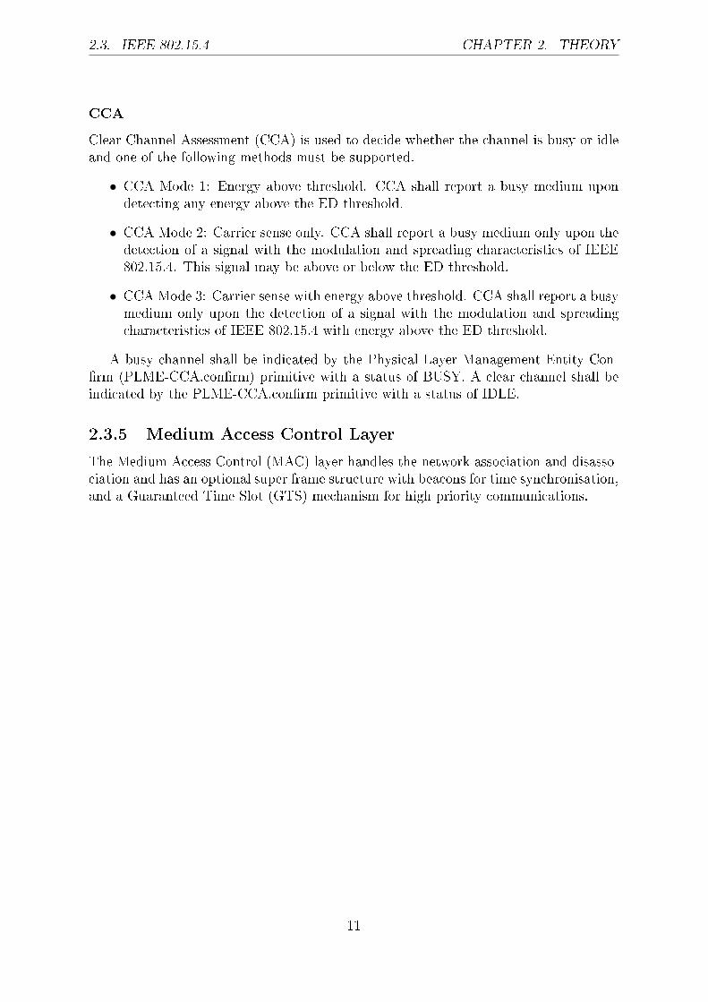
CCA
Clear Channel Assessment (CCA) is used to decide whether the channel is busy or idleand one of the following methods must be supported.
• CCA Mode 1: Energy above threshold. CCA shall report a busy medium upondetecting any energy above the ED threshold.
• CCA Mode 2: Carrier sense only. CCA shall report a busy medium only upon thedetection of a signal with the modulation and spreading characteristics of IEEE802.15.4. This signal may be above or below the ED threshold.
• CCA Mode 3: Carrier sense with energy above threshold. CCA shall report a busymedium only upon the detection of a signal with the modulation and spreadingcharacteristics of IEEE 802.15.4 with energy above the ED threshold.
A busy channel shall be indicated by the Physical Layer Management Entity Con-rm (PLME-CCA.conrm) primitive with a status of BUSY. A clear channel shall beindicated by the PLME-CCA.conrm primitive with a status of IDLE.
2.3.5 Medium Access Control Layer
The Medium Access Control (MAC) layer handles the network association and disasso-ciation and has an optional super frame structure with beacons for time synchronisation,and a Guaranteed Time Slot (GTS) mechanism for high priority communications.
11

2.4. HARDWARE CHAPTER 2. THEORY
2.4 Hardware
There are currently an increasing number of manufactures of IEEE 802.15.4 2.4 GHztransceiver chips. Table 2.4 shows a short comparison of the 2.4 GHz transceiver chipsthat are currently (Q1 2005) on the market.
Table 2.4: 2.4GHz transceiversManufacturer Chip IRX ITX Sensitivity Rx Output Power Voltage
(mA) (mA) (dBm) (dBm) (volts)
Chipcon CC2420 19.7 17.4 -94 0 2.1-3.6
Ember EM2420 19.7 17.4 -94 0 2.1-3.6
Freescale MC13191 37 30 -91 3.6 2-2.4
Freescale MC13192 37 30 -92 3.6 2-3.4
Freescale MC13193 37 30 -92 3.6 2-3.4
CompXs CX1540 57 56 -90 3 2.7-3.3
Ubec uz2400 x x -93 0 x
The table does not show if the chip has extra features, such as an built-in ZigBeestack, ADC or DAC. Currently (Q1 2005) there is no single chip solution (Radio +Microcontroller) on the market, but there may be single chip solutions on the marketlater in this year (2005).
2.5 Security
There are three types of security modes dened: unsecured mode, access control list andsecured mode.
2.5.1 Unsecured mode
No security used.
2.5.2 Access control list
No encryption used, but the network rejects frames from unknown devices.
2.5.3 Secured mode
In the secured mode the devices can use the following security services.
• Access control list.
• Data encryption using the Advanced Encryption Standard (AES) 128 bit encryp-tion algorithm.
12

2.6. ZIGBEE STACK CHAPTER 2. THEORY
• Frame integrity is a security service that uses a Message Integrity Code (MIC)to protect data from being modied by parties without the cryptographic key. Itfurther provides assurance that data come from a party with the cryptographickey.
• Sequential freshness is a security service that uses an ordered sequence of inputsto reject frames that have been replayed. When a frame is received, the freshnessvalue is compared with the last known freshness value.
2.6 ZigBee Stack
In this project the ZigBee software stack from Figure 8Wireless has been used. Currently(Q1 2005) there are just a few companies providing the stack for ZigBee. A short listcan be seen in Table 2.5. Since the ocial standard (ver. 1.0) is not published yet (Q12005), there might be some small changes in the stacks that are currently released.
Table 2.5: ZigBee stackProvider Comment
Figure 8 The one used in this thesis
Stonestreet one
Ember
Microchip Free stack, but not complete
Luxoft Labs
Helicomm
13

2.7. ZIGBEE NETWORKING CHAPTER 2. THEORY
2.7 ZigBee Networking
ZigBee can use so-called mesh networking, which may extend over a large area andcontain thousands of nodes. Each FFD in the network also acts as a router to directmessages. The routing protocol optimizes the shortest and most reliable path throughthe network and can dynamically change, so as to take evolving conditions into account.This enables an extremely reliable network, since the network can heal itself if one nodeis disabled. This is very similar to the redundancy employed in the Internet. ZigBee
Figure 2.5: Mesh network
networks are primarily intended for low duty cycle sensor networks (<1%). A newnetwork node may be recognized and associated in about 30 ms. Waking up a sleepingnode takes about 15 ms, as does accessing a channel or transmitting data. ZigBeeapplications benet from the ability to quickly attach information, detach, and go todeep sleep, which results in low power consumption and extended battery life.
14

Chapter 3
Design Process
The design is made using the CAD program Protel DXP 2004. By using DXP 2004 itis possible to have the schematics and layout designs in the same program environment.The design process is basically carried out in two steps. First, the schematics is designed.Second, the schematics is transferred to a layout. With the layout it is possible tomanufacture Printed Circuit Boards.
As previously mentioned the main task of the project was to develop fully functionalZigBee modules. It was decided to develop two dierent modules. One module thatcontains both an Radio Frequency part (RF) and a Microcontroller part (MCU), whichis called "RF+MCU module". The other module only contains the RF part of thesystem, hereafter called "RF module". The RF module can be used when dierentMCUs are evaluated. The RF+MCU module is preferably used when developing acompletely new application. The RF-part is in the two modules identical.
3.1 Design Description
Figure 3.1 shows the block diagram of the RF+MCU module. The circuit is described indetail in the following sections. Note that the complete schematic and Bill Of Materials(BOM) for both modules are included in Appendix C and D.
3.2 Components
The system is divided into two main parts i.e., RF and MCU. The RF part handles theactual radio system, including Balanced to Unbalanced (BalUn) components, a matchingnetwork (MN) and an antenna. The MCU part handles the digital interface and thecontrol circuit.
3.2.1 Microcontroller Unit
The MCU used is the ATmega128L chip from Atmel. The ATmega128L chip is fully ca-pable of operating the ZigBee software stack, since it contains 128 kB of Flash memory.For an FFD the required memory size is up to 32 kB. The circuit shown in Figure 3.2shows only the essential connections for this application. These are the connections
15

3.2. COMPONENTS CHAPTER 3. DESIGN PROCESS
Figure 3.1: RF+MCU module block diagram
required to program and communicate with the device, and to interface the microcon-troller with the RF transceiver. The complete schematic can be found in AppendixC.
Programming
The modules are designed to support In-System Programming (ISP) via the JTAG inter-face. The connections required to program the device using an in-system programmerare listed in Table 3.1. In this design, these signals are routed to a connector (JP1)which then connects to a programmer. To convert the connector style to a standardJTAG connector a converter is needed. See Appendix D for details. The used in-systemprogrammer is the AVR JTAGICE mkII from Atmel. It is a very powerful programmerthat also supports debugging using the JTAG interface.
Table 3.1: Atmel ATmega128L JTAG interfaceConnection Name Pin Number (Port) Function
TDI 54 (PF7) Test Data Input
TDO 55 (PF6) Test Data Output
TMS 56 (PF5) Test Mode Select
TCK 57 (PF4) Test Clock
3.3V 21, 52 Target Power
GND 22, 63 Common Ground
Reset 20 Target Reset Input
The JTAG programming method is just one of many dierent alternatives. It is upto the user to decide which one is the most suitable alternative. For more informationon alternative programming interfaces, one can refer to [5].
16

3.2. COMPONENTS CHAPTER 3. DESIGN PROCESS
Figure 3.2: MCU circuit
Data Interface
The RF+MCU module has a wide range of external data interfaces, this allows theMCU to communicate with almost any external device. As already mentioned theJTAG interface is very useful when debugging an application. The JTAG interfaceis also used to program the MCU. The Serial Peripheral Interface (SPI) is used tocommunicate with the RF transceiver. The SPI interface can also be used to connectother devices to the module. The SPI interface is described more in the Section 3.2.2.One very commonly used interface is the Universal Synchronous and AsynchronousSerial Receiver and Transmitter (USART). The USART is used to communicate with forexample a RS-232 or USB chip. The USART uses in particular two pins: Receive Data(RXD) and Transmit Data (TXD). Some devices, i.e., modems, also use for exampleReady To Send (RTS) and Clear To Send (CTS) signals. There are several I/O pinsthat can be used for that purpose. The USART allows the MCU to communicatewith any logic-level USART device that supports standard baud rates. There are twoUSARTs on the module connector. To add even more functionality to the module, theTwo Wire Interface (TWI) is routed to the connector. The TWI is fully compatiblewith the well known I2C standard from Philips. The TWI uses only two pins; oneclock pin and one data pin. The interface can be used to communicate with a widerange of devices. There are several pins on the module connector that can be used asGeneral Purpose Input/Output (GPIO) pins. Even some analog pins are routed to theconnector, which allows for the user to use the integrated 10-bit ADC of the MCU. For
17
3.2. COMPONENTS CHAPTER 3. DESIGN PROCESS
additional information please see [5].
Crystals
As shown in Figure 3.2, two external crystals are required for the microcontroller circuit.First, an 8.000 MHz crystal (X2) is used along with two loading capacitors (C1 and C2)to generate the system clock of the MCU. It is also possible to use the internal RC-clock,but to meet the timing accuracy requirement of the IEEE 802.15.4 it is necessary to usean external crystal. Since the crystal is ultimately used to generate the MAC timing, itmust have an overall accuracy of ±40 ppm. Please note that the total accuracy includesinitial tolerance, temperature drift and aging. There are several factors to consider whenselecting the 8.000 MHz crystal. One of the goal for this module was to reduce the sizeas much as possible, therefore a 5x7 mm crystal is used. For applications that are morecost-sensitive, a larger package such as the industry-standard HC-49 can be used. Toreduce the cost even more the temperature tolerance can be relaxed. Which package touse is of course application dependent.
The second external crystal, X3, is the Real Time Clock (RTC). The RTC is a 32.768kHz watch crystal. This crystal is required for the internal low-frequency timer/counteroscillator which is used when the device is in power-save mode. The MCU has integratedloading capacitors, which makes external loading capacitors unnecessary. The frequencyof the RTC is chosen such that it is possible to use hours and minutes for the wake-uptime of the device, for instance.
3.2.2 RF Transceiver/Microcontroller Conguration and DataInterface
The interface between the RF and MCU parts is illustrated in Figure 3.1. Table 3.2provides a description of these interface signals.
The SPI interface is a commonly used interface for connecting several peripheralunits to one microcontroller. The interface uses four lines, i.e., CSn, SCLK, SI andSO, as described in Table 3.2. To be able to connect several devices on the SPI busit is necessary to connect a 0 Ω resistor (R312) in series on the SCLK line, to avoidcontention on the line. See Figure 3.2. The resistor allows other devices to drive theSCLK line without damaging the CC2420 chip.
The VREG_EN signal is connected to a pull-down resistor (R315) to make sure thatthe internal voltage regulator is disabled when the microcontroller is reset.
Please note that both the series resistor (R312) and the pull-down resistor (R315)are not implemented on the RF module, because dierent MCUs has dierent ways ofconnecting to the SPI bus.
More information about the RF Transceiver/Microcontroller Conguration and DataInterface can be found in [4].
3.2.3 RF Circuit
The RF circuit is shown in Figure 3.3. The gure shows all the external componentsrequired for the CC2420 to work properly. Note that no decoupling capacitors are
18

3.2. COMPONENTS CHAPTER 3. DESIGN PROCESS
Table 3.2: RF Transceiver/Microcontroller interface
RF RF MCU MCU
Num. Name Description Num. Name
21 RESETn Asynchronus, active low digital reset. 16 PB6
27 SFD Start of Frame Delimiter. 29 PD4
28 CCA Clear Channel Assessment. 31 PD6
29 FIFOP Asserted when last packet has been receivedor FIFO size has exceeded threshold.
6 INT4
30 FIFO Asserted when data is present in FIFO. 7 PE5
31 CSn SPI Chip Select, active low. 10 SSn
32 SCLK SPI Clock input, up to 10 MHz. 11 SCK
33 SI SPI Slave Input. Sampled on the positiveedge of SCLK.
12 MOSI
34 SO SPI Slave Output. Updated on the negativeedge of SCLK. Tristate when CSn is high.
13 MISO
41 VREG_EN Internal voltage regulator enable, activehigh.
15 PB5
included in the schematic. It is important to note that in this design the RF transceiveris congured for unbalanced (or single-ended) operation. The RF transceiver can alsobe used for balanced (or dierential) operation. However, this is not discussed in thisdocument.
BalUn and Matching Network
The RF input/output port of the RF transceiver is a dierential and high impedanceport. To be able to use the RF transceiver in single-ended mode, a BalUn circuit isneeded. BalUn stands for Balanced-Unbalanced. The optimal dierential load for theRF transceiver is 115+j180 Ω.
The BalUn circuit in this design is used for dierent functions. The typical functionof a BalUn is to convert the dierential RF input/output signal to a single-ended port.In Figure 3.3 component pairs L62/C61 and L81/C81 accomplish this task by shiftingsignals RF−P and RF−N by 90. This is equivalent to shifting the phase 180 relativeto each other, resulting in an single-ended signal.
The second function performed by the BalUn is impedance matching. All the valuesof the components are carefully chosen so that the impedance "looking into" the BalUnis 50 Ω. The values of the components are exactly the same as the reference designavailable from Chipcon, however the values are carefully controlled and re-calculatedusing the Smith Chart Utility in Advanced Design System 2003C (ADS2003C). Formore information refer to Appendix A.
The last function of the BalUn is to provide the needed DC bias to the internal PAand LNA in the RF transceiver. A DC patch must exist from the pin TXRX−SWITCHto the pins RF−P and RF−N. This is accomplished by the inductors L61 and L62.
19
3.2. COMPONENTS CHAPTER 3. DESIGN PROCESS
Figure 3.3: RF circuit
The capacitor C71 is used for decoupling. Finally the capacitor C63 is a DC blockingcapacitor to the antenna and matching network.
Antenna
The antenna used in the design is the Mica antenna from gigaAnt AB. It is a relativelysmall antenna of SMD type which requires a ground plane for proper placement. Theantenna has a length of a quarter wave length at 2.4 GHz. One important factor whendesigning the modules was the radio range. The Mica antenna has a fairly high eciency,75%, which results in a good range of the radio link.
Crystal
An external 16.000 MHz crystal (X1) is needed for the RF transceiver to work. Twoloading capacitors (C381 and C391), shown in Figure 3.3, are required for the internaloscillator circuit. When selecting the crystal it is important to notice that the EquivalentSerial Resistans (ESR) must be 60 Ω or less. Otherwise one can not guarantee the start-up time of the internal oscillator. Another thing to notice is that the overall accuracymust not exceed ±40 ppm. The overall accuracy includes temperature drift, initialtolerance and aging. For applications where IEEE 802.15.4 compliance is not requiredthe overall accuracy can be relaxed to ±60 ppm.
20

3.3. PRINTED CIRCUIT BOARD LAYOUT CHAPTER 3. DESIGN PROCESS
Bias Resistor
The bias resistor (R451), shown in Figure 3.3, is used to set an accurate current for theinternal current regulator. A 43 kΩ resistor with 1% tolerance must be used.
Voltage Regulator
The RF transceiver is equipped with an internal voltage regulator which is used to powerall of the 1.8V power supply. A 10 µF tantalum capacitor (C421) is required to securethe stability of the regulator. The ESR of the tantalum capacitor must be between 0.5and 5 Ω. As seen in Figure 3.3 a series resistor (R421) is used to prevent the ESR todrop below 0.5 Ω. The ESR will vary with the temperature.
Power Supply Decoupling
To ensure optimal performance a good power supply decoupling is needed. As usual theplacement and size of the decoupling capacitors are very important. The placement ofthe decoupling capacitors is described more closely in the Chapter 4.
3.2.4 Connector
The connector used in the design is a small SMD connector from HRS. The connectorhas 20 pins which is enough for all important signals. When designing the modulesone primary task was to make it easy to connect the modules with dierent kinds ofapplications. This is fullled with this connector. Since the only connection of themodule to the application board is via the connector, the stability of the connector isimportant. The used connector has a "snap-in" function, so the stability is ensured.
3.2.5 Power Supply
The power to the RF+MCU module is supplied by a low drop-out voltage regulatorREG102 from Texas Instruments Inc. The new DMOS topology provides a very lowdrop-out and good protection against transients. The REG102 has thermal and overcurrent protection functions, including a fold back current limit. The regulator also hasvery low output noise (typically 28 µVRMS for VOUT 3.3 V), which makes it ideal foruse in small communications devices.
3.3 Printed Circuit Board Layout
A proper designed Printed Circuit Board (PCB) is very important for the operation ofthe RF Transceiver. This section describes the layout design process of the modules.
3.3.1 PCB Overview
The PCB of the two modules is a 4 layer standard FR-4 board. The board is 0.95 mm inthickness. The dimensions of the RF+MCU module is 23x40 mm, and the RF module is
21

3.3. PRINTED CIRCUIT BOARD LAYOUT CHAPTER 3. DESIGN PROCESS
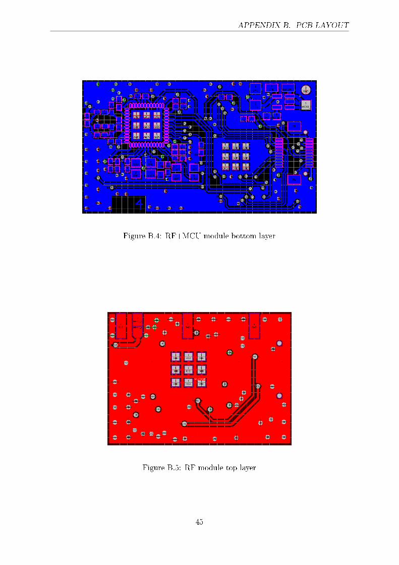
18x25 mm. The components on the RF+MCU module are placed on both the top andbottom layer, as shown in Figure 3.4. The only component on the RF module which isplaced on the top side is the antenna, while the rest of the components are placed onthe bottom layer, see Figure 3.5.
Figure 3.4: RF+MCU module Figure 3.5: RF module
The board is composed of four layers shown in Figure 3.6. The two internal layersare used for power and ground. While the top and bottom layers are used for routing.On the top and bottom a copper pour connected to ground is used. The complete setof PCB layout les can be found in Appendix B. All the design parameters are selectedfor fabrication in a standard low-cost production process. The smallest via diameter is0.3 mm, and the smallest trace width is 0.15 mm. The components used on the twomodules are mainly of size 0402.
Figure 3.6: Layer stackup
3.3.2 General Layout Guidelines
One very important factor when working with RF designs is that power supply decou-pling is implemented properly on the PCB. All decoupling capacitors should be as smallas possible (preferably 0402) to reduce parasitics. For best results decoupling capacitorsshould be placed as close to the chip pins as possible. To maximize the eectivenessof decoupling, the capacitors were placed between the pins and the via to the internalpower plane. Placing vias between the supply pin and the capacitor should be avoided.
22
3.3. PRINTED CIRCUIT BOARD LAYOUT CHAPTER 3. DESIGN PROCESS
All connections to ground for component pins and decoupling capacitors should beas short as possible. It is very important that every connection to ground is made via anindividual connection to the internal ground plane. It is not recommended to rely solelyon the top and bottom layer copper pour, as it can result in oating ground planes.
The traces between the 16.000 MHz crystal and the RF transceiver should be veryshort. The loading capacitors are placed in-line with the traces.
The connection between the antenna and the single-ended port of the BalUn ismade via a controlled impedance microstrip line. The width of the microstrip lineis determined based on several parameters, including 50 Ω impedance, ground planeseparation and the dielectric constant of the PCB substrate. To calculate the width ofthe microstrip line the function "characteristic impedance driven width" in Protel DXP2004 is used. The width is calculated to be 0.4917 mm to obtain a 50 Ω micro strip line.The antenna is placed on the top layer, connected via the microstrip line through a viato the BalUn.
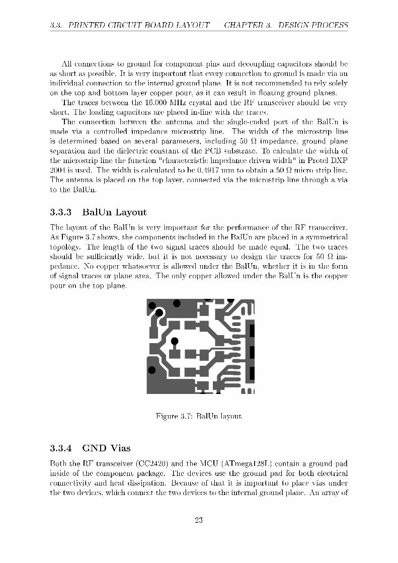
3.3.3 BalUn Layout
The layout of the BalUn is very important for the performance of the RF transceiver.As Figure 3.7 shows, the components included in the BalUn are placed in a symmetricaltopology. The length of the two signal traces should be made equal. The two tracesshould be suciently wide, but it is not necessary to design the traces for 50 Ω im-pedance. No copper whatsoever is allowed under the BalUn, whether it is in the formof signal traces or plane area. The only copper allowed under the BalUn is the copperpour on the top plane.
Figure 3.7: BalUn layout
3.3.4 GND Vias
Both the RF transceiver (CC2420) and the MCU (ATmega128L) contain a ground padinside of the component package. The devices use the ground pad for both electricalconnectivity and heat dissipation. Because of that it is important to place vias underthe two devices, which connect the two devices to the internal ground plane. An array of
23

3.3. PRINTED CIRCUIT BOARD LAYOUT CHAPTER 3. DESIGN PROCESS
3x3 vias is used for both devices, which minimizes the thermal resistance and providesa solid ground connection. This is shown in Figure 3.8.
Figure 3.8: Ground vias (bottom view)
To avoid oating ground planes and parasitic eects the copper pour areas are con-nected to the internal ground plane with several vias. This will prevent unwantedresonances that could potentially impact the RF performance.
24

Chapter 4
Implementation
This chapter describes the implementation of the design, and the fully functional ZigBeemodules developed.
4.1 PCB Manufacturing
Since the PCBs in this design have four layers, it is not possible to manufacture itin the PCB lab at the university. The company Elektrotryck AB was contracted tomanufacture the modules. Elektrotryck handled all the panelization of the modules. Atotal of 40 modules was manufactured, 20 pieces of each module.
Before manufacturing the layout les must be converted into a format that can bemanaged by the PCB manufacturer, in this case Gerber RS274X. This results in a setof les, where each le contains information about a specic layer.
For this design the following layers were used:
• Topoverlay - Component print on top.
• Topsolder - Top solder mask.
• Top - Copper on top layer.
• Plane1 - Power/ground plane, negative.
• Plane2 - Ground plane, negative.
• Bottom - Copper on bottom layer.
• Bottomsolder - Bottom solder mask.
• Bottomoverlay - Component print on bottom.
• Drill - Drill le, in .exc format.
• Prole - The milling le, i.e., the shape of the modules.
25

4.2. ASSEMBLY CHAPTER 4. IMPLEMENTATION
4.2 Assembly
All the assembly was performed at the university. Since there was no ip-chip mountingequipment at the institution, the most dicult part of the assembly was the mountingof the ICs. The assembly was performed with a microscope.
4.3 Soldering
To make it possible to manufacture the small modules in-house, a reow soldering ovenwas purchased. With a reow soldering oven it is pretty easy to get a good result whensoldering small components.
4.4 Bill Of Material
The Bill Of Material (BOM) for the two modules is to be seen in Appendix D. TheBOM is created using Protel DXP 2004.
4.5 Assembled Modules
The overall dimension of the RF+MCU module is 23x40 mm, and the RF module is18x23 mm. Table 4.1 shows the dimensions that have been used for the RF+MCUmodule.
Table 4.1: PCB dimensions for RF+MCU moduleDescription Dimension
Standard track width 0.2 mm
Via hole size 0.3 mm
Via pad size 0.6 mm
Standard component size 0402
No of vias 131
No of components 50
Table 4.2 shows the pin list of the RF+MCU module, and Table 4.3 shows the pinlist of the RF module. For more information about the these modules please refer toChapter 3.
26

4.5. ASSEMBLED MODULES CHAPTER 4. IMPLEMENTATION
Table 4.2: RF+MCU module pin listPin no. Pin Description and
Name internal MCU connection
1 SCLK SPI interface clock, PB1.
2 SI SPI interface Slave Input, PB2.
3 SO SPI interface Slave Output, PB3.
4 SCL TWI (I2C) clock, PD0.
5 SDA TWI (I2C) data, PD1.
6 PD2 UART RXD1, Digital I/O, PD2.
7 PD3 UART TXD1, Digital I/O, PD3.
8 PD5 Digital I/O, PD5.
9 PD7 Digital I/O, PD7.
10 GND GND
11 3.3V Power
12 AREF Analogue ref. for internal ADC.
13 RESET Reset
14 TXD0 UART TXD0, Digital I/O, PE1.
15 RXD0 UART RXD0, Digital I/O, PE0.
16 PF3 Digital or Analogue I/O, PF3.
17 TCK Digital or Analogue I/O, JTAG TCK, PF4.
18 TMS Digital or Analogue I/O, JTAG TMS, PF5.
19 TDO Digital or Analogue I/O, JTAG TDO, PF6.
20 TDI Digital or Analogue I/O, JTAG TDI, PF7.
27

4.5. ASSEMBLED MODULES CHAPTER 4. IMPLEMENTATION
Table 4.3: RF module pin listPin no. Pin Description
Name
1 VREG_EN Internal voltage regulator enable, activehigh.
2 SFD Start of Frame Delimiter.
3 CCA Clear Channel Assessment.
4 FIFO Asserted when data is present in FIFO.
5 FIFOP Asserted when last packet has been receivedor FIFO size has exceeded threshold.
6 CS SPI Chip Select, active low.
7 SCLK SPI Clock input, up to 10 MHz.
8 SI SPI Slave Input. Sampled on the positiveedge of SCLK.
9 SO SPI Slave Output. Updated on the negativeedge of SCLK. Tristate when CSn is high.
10 VREG_IN Power, 3.3V
11 GND GND
12 NC No Connection.
13 NC No Connection.
14 NC No Connection.
15 NC No Connection.
16 NC No Connection.
17 NC No Connection.
18 NC No Connection.
19 RESETn Asynchronous, active low digital reset.
20 GND GND
28

Chapter 5
Development Tools
A range of dierent software and hardware tools are used to compile and congure themodules. The development environment is a combination of the programs and devicespresented here.
5.1 CC2420 ZigBee DK Development Kit
The CC2420 ZigBee DK Development Kit was purchased from Chipcon, and used toevaluate the ZigBee and IEEE 802.15.4 standards. The kit contains seven laborationcards with dierent integrated sensors and devices. One packet snier is also included inthe kit. The packet snier is used to read out the packets sent over the air. It is a veryuseful tool when working with wireless devices. The CC2420 ZigBee DK DevelopmentKit also contains the ZigBee software stack. The stack is recongured for use with thetwo developed modules. The complete kit is shown in Figure 5.1.
Figure 5.1: CC2420 ZigBee DK Development Kit
29

5.2. ATMEGA128L TOOLS CHAPTER 5. DEVELOPMENT TOOLS
5.2 ATmega128L Tools
The use of the microcontroller ATmega128L from Atmel is based on some dierent tools.
5.2.1 AVR GCC Tool
The free GNU AVR GCC development tools are used to generate the les for theRF+MCU module running on the ATmega128L controller. The GNU AVR GCC com-piler is used when compiling les with Programmer's Notepad. Please see [13] in orderto obtain detailed insight in compiler options and make-les etc.
5.2.2 Atmel AVR Studio
The AVR Studio is used to download code to the microcontroller on the RF+MCUModule. Together with the programmer AVR JTAG ICEmkII is also used for debugging.Figure 5.2 shows the user interface of AVR studio.
Figure 5.2: AVR studio
30

5.2. ATMEGA128L TOOLS CHAPTER 5. DEVELOPMENT TOOLS
5.2.3 Programmer's Notepad
A text editor such as Programmer's Notepad with highlighting is used for source codewriting. The editor is congured to run the make-les, by use of macros linked to themake-les for AVR GCC. As seen in Figure 5.3 the code is divided automatically intodierent sections.
Figure 5.3: Programmer's Notepad
31
5.3. PCB TOOL CHAPTER 5. DEVELOPMENT TOOLS
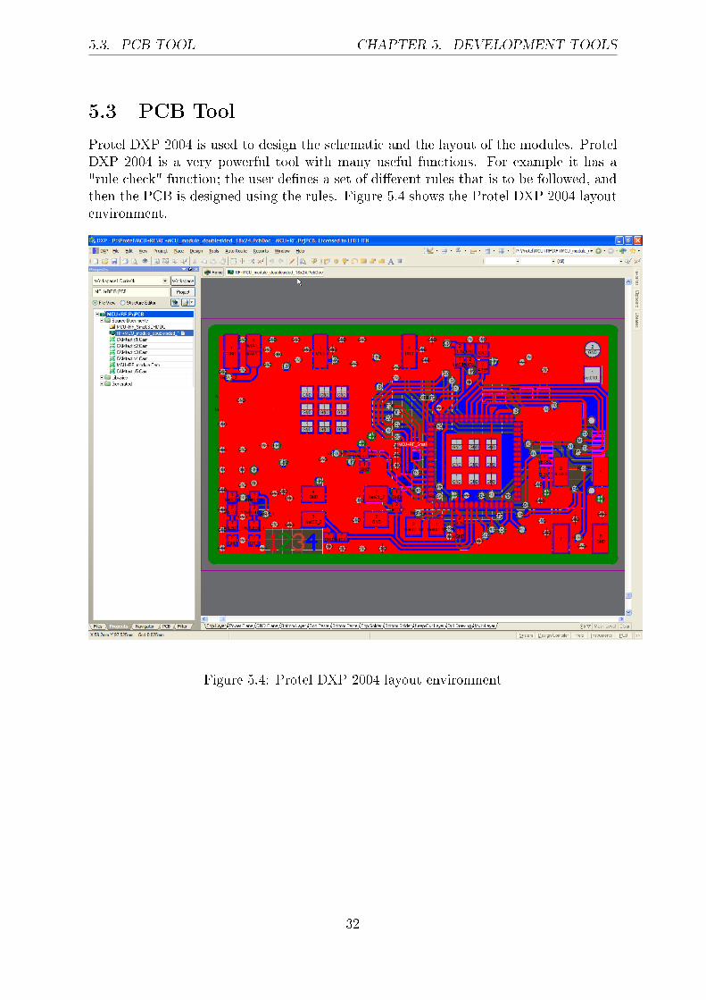
5.3 PCB Tool
Protel DXP 2004 is used to design the schematic and the layout of the modules. ProtelDXP 2004 is a very powerful tool with many useful functions. For example it has a"rule check" function; the user denes a set of dierent rules that is to be followed, andthen the PCB is designed using the rules. Figure 5.4 shows the Protel DXP 2004 layoutenvironment.
Figure 5.4: Protel DXP 2004 layout environment
32

Chapter 6
Test Application
To test and evaluate the developed ZigBee and IEEE 802.15.4 modules a test appli-cation has been developed. The test application consists of two devices: a networkcoordinator which displays the temperature value on a display, and a temperature sen-sor which reports the current temperature value to the coordinator. The ZigBee andIEEE 802.15.4 modules are connected to the test devices. As previously stated that thedeveloped ZigBee modules should be able to easily connect themselves to dierent typesof applications. The two test devices has been developed and assembled in-house.
33

6.1. TEMPERATURE COORDINATOR CHAPTER 6. TEST APPLICATION
6.1 Temperature Coordinator
The coordinator display device consists of a 2-layer PCB, as seen in Figure 6.1. TheZigBee module is connected via a connector to the PCB. The display is connected tothe MCU on the module via the same SPI interface as the RF transceiver (CC2420).The coordinator device in the test application is responsible for setting up a network.When the network is set up, the coordinator device initiates the display, and then itwaits for the temperature sensor device to report a temperature value. When a valueis received the coordinator device converts it to ASCII characters, and the ASCII valueare displayed. Figure 6.2 shows the complete MCU program ow.
Figure 6.1: Temperature coordinator Figure 6.2: Temperature coordinator ow
34

6.2. TEMPERATURE SENSOR CHAPTER 6. TEST APPLICATION
6.2 Temperature Sensor
The temperature sensor device is developed with the temperature sensor DS1631 fromMaxim/Dallas Semiconductor. The temperature sensor is connected to the MCU on theZigBee and IEEE 802.15.4 module via the TWI (I2C) bus, see Figure 6.3.
The temperature sensor device in the test application connects itself wirelessly tothe coordinator of the network. When the temperature sensor device is connected to thenetwork the temperature sensor is initiated. A 12-bit value from the temperature sensoris then read and sent to the coordinator device. After that the temperature device is inrest for about two seconds, and then a new value is read from the temperature sensor.Figure 6.4 shows the complete MCU program ow.
Figure 6.3: Temperature sensor ow Figure 6.4: Temperature sensor ow
35

Chapter 7
Results
This thesis work has shown that ZigBee can be seen as a complement to other standards,i.e., Bluetooth and IEEE 802.11 WLAN. ZigBee is not competing in the same marketsegment as either Bluetooth or WLAN. One very important factor for the success ofZigBee is the interoperability. A remote controller from, i.e., Philips must be ableto operate a Samsung TV. The three major advantages of ZigBee are low price, longcovering range and low energy consumption.
The developed modules can be used for quick prototyping of small wireless sensors,and build large sensor networks. To verify the functionality of the modules, a testapplication has also been developed. The test application consists of a PAN coordinatorand a temperature sensor FFD device. The temperature sensor device reports thetemperature to the coordinator which displays the temperature on a display.
The other module, i.e., the RF module is preferably used when evaluating dierentMCUs. When developing new ZigBee applications the RF+MCU module will be used.
36

Chapter 8
Discussions
The market for wireless sensor networks is expected to grow rapidly in the near future.Our developed ZigBee-ready modules may contribute to this development, since theycan easily be connected to various type of sensors and to build up wireless networks.
Our modules are small, but the size can be reduced even more, when a single-chipsolution is on the market. (Which is expected in Q2 2005.)
If the ZigBee interoperability work between dierent brands of ZigBee devices, theZigBee standard may be the dominating standard for wireless sensor networks in thefuture.
One important advantage of ZigBee over other wireless standards is the low price.The price for one IEEE 802.15.4 transceiver chip is currently as low as < $3. One shouldalso notice that the IEEE 802.15.4 transceiver can be used to build custom networks,without using the ZigBee network structure.
37

Chapter 9
Conclusions
We believe that there is denitely a place on the market for ZigBee, since no globalstandard exists today in the wireless sensor network area.
Two fully functional ZigBee/802.15.4 modules have been developed. It is possibleto design a module with RF parts on a low cost FR-4 PCB substrate. By using a fourlayer PCB the size is reduced signicantly.
Finally it is shown that a temperature sensor can be integrated with the developedZigBee-ready modules.
38
Chapter 10
Further work
Some suggestions of further work are given below.The modules can be improved by:
• Smaller PCB.
• New RF-chip with integrated MCU (May be released from Chipcon in Q2 2005).
• Smaller or integrated antenna.
• Integrated sensors on the module.
Suggested further work for ZigBee enabled applications are:
• USB gateway, for easy communication with a PC.
• Dierent kinds of sensors, e.g., temperature, pressure, ow, moisture, humidityand accelerometers, etc.
• PC program for control of the ZigBee network.
39
Bibliography
[1] Reinhold Ludvig and Pavel Bretchko, RF Circuit Design - Theory and Applications,Prenctice Hall 2000, ISBN 0-13-095323-7.
[2] William Stallings, Wireless Communication and Networking, Prenctice Hall 2002,ISBN 0-13-040864-6.
[3] IEEE Standards 802.15.4, IEEE 2003, ISBN 0-7381-3677-5 SS95127.
[4] Chipcon AS, Chipcon AS SmartRF CC2420 Preliminary Data sheet (rev 1.2)
[5] Atmel Corporation, ATmega128L Data sheet Rev. 2467M-AVR-11/04
[6] ZigBee Alliance, http://www.zigbee.org, 2005-03
[7] Freescale Semiconductor, http://www.freescale.com, 2005-03
[8] Maxim-Ic, http://www.maxim-ic.com, 2005-03
[9] Atmel Corporation, http://www.atmel.com, 2005-03
[10] Chipcon, http://www.chipcon.com, 2005-03
[11] gigaAnt, http://www.gigaant.com, 2005-03
[12] Figure 8 Wireless, http://www.gure8wireless.com, 2005-03
[13] AVR Freaks, http://www.avrfreaks.com, 2005-03
[14] Texas Instruments, http://www.ti.com, 2005-03
40

Appendices
41

Appendix A
Tools
The Smith Chart tool in ADS can be used to create matching networks.
Figure A.1: Smith Chart tool in ADS
42

Appendix B
PCB Layout
Figure B.1: RF+MCU module top layer
43

APPENDIX B. PCB LAYOUT
Figure B.2: RF+MCU module power/GND plane, negative
Figure B.3: RF+MCU module GND plane, negative
44
APPENDIX B. PCB LAYOUT
Figure B.4: RF+MCU module bottom layer
Figure B.5: RF module top layer
45

APPENDIX B. PCB LAYOUT
Figure B.6: RF module power/GND plane, negative
Figure B.7: RF module GND plane, negative
46

APPENDIX B. PCB LAYOUT
Figure B.8: RF module bottom layer
47
Appendix C
Schematics
Schematics for the RF+MCU Module, the RF Module and the JTAG connector ispresented here.
48

APPENDIX C. SCHEMATICS
11
22
33
44
55
66
77
88
DD
CC
BB
AA
Title
Num
ber
Rev
isio
nSi
ze A2
Dat
e:20
05-0
2-14
Shee
t o
fFi
le:
Y:\U
tbild
ing\
..\M
CU
+RF_
Smal
l.SC
HD
OC
Dra
wn
By:
16pF
C1
16pF
C2
3.3V
10nF
C4
10nF
C5
10nF
C6
100n
FC
7
3.3V
0.01
uFC
8
JP2
2
31
4
X2
3.3V
V_i
n1
GN
D2
Enab
le3
NR
4
Vou
t5
REG
102
10uF
C9
E1
0.1u
FC
10
0R
312
100K
R31
5
C35
1C
261
C17
1C
251
C11
C10
1C
371
C44
1C
481
C39
1C
381
R45
1
1.8V
3.3V
1.8V
3.3V
1.8V
R42
1
C61
C63
C81
C71
L62
L81
L61
FIFO
FIFO
PC
CA
SFD
CS
SI SOSCLK
C43
1C
421
RES
ETn
VR
EG
_EN
11
22
33
44
X1
NX
4025
DA
FIFO
FIFO
P
CC
A
SFD
CS
SCLK
SI SO VR
EG
_EN
RES
ETn
GN
D9
RF_
N8
AV
DD
_CH
P48
AV
DD
_IF1
44
AV
DD
_RF1
4
DV
DD
3.3
25
N/C
11
N/C
12
N/C
13
SFD
27
CS
31
GN
D5
SCLK
32
AV
DD
_AD
C17
DV
DD
_AD
C18
DG
UA
RD20
DV
DD
_1.8
26
N/C
40
CC
A28
N/C
36
SI33
RES
ET21
SO34
VR
EG
_IN
43
FIFO
30
FIFO
P29
VR
EG
_EN
41
VR
EG
_OU
T42
XO
SC_Q
139
RB
IAS
45
XO
SC_Q
238
DG
ND
_CO
RE
24
RF_
P6
DG
ND
_PA
DS
23
AV
DD
_IF2
15
DG
ND
22D
GN
D_G
UA
RD
19
N/C
16
DV
DD
_RA
M35
AV
DD
_RF2
14A
VD
D_S
W10
AV
DD
_PR
E3
AV
DD
_VC
O2
VC
O_G
UA
RD
1
AV
DD
_XO
SC37
TXR
X_S
WIT
CH7
AT
EST2
46
AT
EST3
47
U1
CC
2420
PD5
PD3
PD2
PD7
SDA
SCL
3.3V
AR
EF
GN
D
RES
ET
GN
D
SCLK
SI SO SCL
SDA
PD2
PD3
PD5
PD7
TDI
TDO
TMS
TCK
PF3
TDI
TDO
TMS
TCK
PF3
RES
ETA
RE
F3.
3V
47K
R1
47K
R2
11
22
X3
FOX
32.
768M
Hz
LED
1
RX
D0
TXD0
RX
D0
TXD
0
LED
2
68R3
68R4
11
33
22
44
S1
PEN
1
PE0
(RX
D0/
PDI)
2
PE1
(ALE
)3
PE2
(XC
K0/
AIN
0)4
PE3
(OC
3A/A
IN1)
5
PE4
(OC
3B/I
NT4
)6
PE5
(OC
3C/I
NT5
)7
PE6
(T3/
INT
6)8
PE7
(IC
3/IN
T7)
9
PB0
(SS)
10
PB1
(SC
K)
11
PB2
(MO
SI)
12
PB3
(MIS
O)
13
PB4
(OC
0)14
PB5
(OC
1A)
15
PB6
(OC
1B)
16
PB7
(OC
2/O
C1C
)17
TOSC
2/PG
318
TOSC
1/1P
G4
19
RES
ET20
VC
C21
GN
D22
XT
AL2
23
XT
AL1
24
PD0
(SC
L/IN
T0)
25
PD1
(SD
A/IN
T1)
26
PD2
(RX
D1/
INT2
)27
PD3
(TX
D1/
INT3
)28
PD4
(IC
1)29
PD5
(XC
K1)
30
PD6
(T1)
31
PD7
(T2)
32
PG0
(WR
)33
PG1
(RD
)34
PC0
(A8)
35
PC1
(A9)
36
PC2
(A10
)37
PC3
(A11
)38
PC4
(A12
)39
PC5
(A13
)40
PC6
(A14
)41
PC7
(A15
)42
PG2
(AL
E)43
PA7
(AD
7)44
PA6
(AD
6)45
PA5
(AD
5)46
PA4
(AD
4)47
PA3
(AD
3)48
PA2
(AD
2)49
PA1
(AD
1)50
PA0
(AD
0)51
VC
C52
GN
D53
PF7
(AD
C7/
TDI)
54
PF6
(AD
C6/
TDO
)55
PF5
(AD
C5/
TMS)
56
PF4
(AD
C4/
TCK
)57
PF3
(AD
C3)
58
PF2
(AD
C2)
59
PF1
(AD
C1)
60
PF0
(AD
C0)
61
AR
EF
62
GN
D63
AV
CC
64
U2
AT
meg
a128
L-8A
I
11
22
33
44
55
66
77
88
99
1010
1111
1212
1313
1414
1515
1616
1717
1818
1919
2020
JP1
G1
F2
S13
S24
A1
PCB
Ant
enna
RF
+ M
CU m
odul
e
R1A
Jona
s O
lsso
n, Jo
han
Lönn
Figure C.1: Schematic of RF+MCU module
49

APPENDIX C. SCHEMATICS
11
22
33
44
55
66
77
88
DD
CC
BB
AA
Title
Num
ber
Rev
isio
nSi
ze A3
Dat
e:20
05-0
2-14
Shee
t o
fFi
le:
Y:\U
tbild
ing\
..\R
F_m
odul
e.Sc
hDoc
Dra
wn
By:
RF
Mod
ule
R1A
C35
1C
261
C17
1C
251
C11
C10
1C
371
C44
1C
481
C39
1C
381
R45
1
1.8V
3.3V
1.8V
3.3V
1.8V
R42
1
FIFO
FIFO
P
CC
ASF
D
CS
SCLK
SI SO
RES
ETN
VR
EG
_EN
VR
EG
_IN
C61
C63
C81
C71
L62
L81
L61
Jona
s O
lsso
n, Jo
han
Lönn
FIFO
FIFO
P
CC
ASF
D
CS
SI SOSCLK
C43
1C
421
RES
ETN
VR
EG
_EN
11
22
33
44
X1
NX
4025
DA
GN
D9
RF_
N8
AV
DD
_CH
P48
AV
DD
_IF1
44
AV
DD
_RF1
4
DV
DD
3.3
25
N/C
11
N/C
12
N/C
13
SFD
27
CS
31
GN
D5
SCLK
32
AV
DD
_AD
C17
DV
DD
_AD
C18
DG
UA
RD
20
DV
DD
_1.8
26
N/C
40
CC
A28
N/C
36
SI33
RES
ET
21
SO34
VR
EG
_IN
43
FIFO
30
FIFO
P29
VR
EG
_EN
41
VR
EG
_OU
T42
XO
SC_Q
139
RB
IAS
45
XO
SC_Q
238
DG
ND
_CO
RE
24
RF_
P6
DG
ND
_PA
DS
23
AV
DD
_IF2
15
DG
ND
22D
GN
D_G
UA
RD
19
N/C
16
DV
DD
_RA
M35
AV
DD
_RF2
14A
VD
D_S
W10
AV
DD
_PR
E3
AV
DD
_VC
O2
VC
O_G
UA
RD
1
AV
DD
_XO
SC37
TXR
X_S
WIT
CH
7
AT
EST2
46
AT
EST3
47
U1
CC
2420
11
22
33
44
55
66
77
88
99
1010
1111
1212
1313
1414
1515
1616
1717
1818
1919
2020
JP1
G1
F2
S13
S24
A1
Figure C.2: Schematic of RF module
50

APPENDIX C. SCHEMATICS
11
22
33
44
DD
CC
BB
AA
Title
Num
ber
Rev
isio
nSi
ze A4
Dat
e:20
05-0
2-14
Shee
t o
fFi
le:
Y:\U
tbild
ing\
..\JT
AG
_Con
n.Sc
hDoc
Dra
wn
By:
JTA
G C
onne
ctor
R1A
Jona
s O
lsso
n, J
ohan
Lön
n
11
22
33
44
55
66
77
88
99
1010
1111
1212
1313
1414
1515
1616
1717
1818
1919
2020
JP1
RF
Con
nect
or
12
34
56
78
910
JP2
JTA
G10
0nF
C1
3.3V
RES
ET
TCK
TMS
TDO
TDI
GN
D
Figure C.3: Schematic of JTAG connector
51

Appendix D
Bill of Material
The Bill of Material for the two dierent modules is presented here.
52

APPENDIX D. BILL OF MATERIAL
Rep
ort
Gen
erat
ed F
rom
DX
P
Des
crip
tio
nD
esig
nat
or
Fo
otp
rin
tL
ibR
efQ
uan
tity
Val
ue
SM
D A
nten
na M
ica
A1
PC
B_A
nten
na_M
ica
PC
B A
nten
na M
ica
1C
apac
itor
(Sem
icon
duct
or S
IM M
odel
)C
1C
C10
05-0
402
Cap
Sem
i1
16pF
Cap
acito
r (S
emic
ondu
ctor
SIM
Mod
el)
C2
CC
1005
-040
2C
ap S
emi
116
pFC
apac
itor
(Sem
icon
duct
or S
IM M
odel
)C
4C
C10
05-0
402
Cap
Sem
i1
10nF
Cap
acito
r (S
emic
ondu
ctor
SIM
Mod
el)
C5
CC
1005
-040
2C
ap S
emi
110
nFC
apac
itor
(Sem
icon
duct
or S
IM M
odel
)C
6C
C10
05-0
402
Cap
Sem
i1
10nF
Cap
acito
r (S
emic
ondu
ctor
SIM
Mod
el)
C7
CC
1608
-060
3C
ap S
emi
110
0nF
Cap
acito
r (S
emic
ondu
ctor
SIM
Mod
el)
C8
CC
1608
-060
3C
ap S
emi
10.
01uF
Cap
acito
r (S
emic
ondu
ctor
SIM
Mod
el)
C9
CC
3216
-120
6C
ap S
emi
110
uFS
olid
Tan
talu
m C
hip
Cap
acito
r, S
tand
ard
T49
4 S
erie
s -
Low
ES
R, I
ndus
tria
l Gra
deC
10A
T49
4A1
0.1u
FC
apac
itor
(Sem
icon
duct
or S
IM M
odel
)C
11C
C10
05-0
402
Cap
Sem
i1
100n
FC
apac
itor
(Sem
icon
duct
or S
IM M
odel
)C
61C
C10
05-0
402
Cap
Sem
i1
0.5p
FC
apac
itor
(Sem
icon
duct
or S
IM M
odel
)C
63C
C10
05-0
402
Cap
Sem
i1
5.6p
FC
apac
itor
(Sem
icon
duct
or S
IM M
odel
)C
71C
C10
05-0
402
Cap
Sem
i1
5.6p
FC
apac
itor
(Sem
icon
duct
or S
IM M
odel
)C
81C
C10
05-0
402
Cap
Sem
i1
0.5p
FC
apac
itor
(Sem
icon
duct
or S
IM M
odel
)C
101
CC
1005
-040
2C
ap S
emi
110
nFC
apac
itor
(Sem
icon
duct
or S
IM M
odel
)C
171
CC
1005
-040
2C
ap S
emi
168
pFC
apac
itor
(Sem
icon
duct
or S
IM M
odel
)C
251
CC
1005
-040
2C
ap S
emi
110
0nF
Cap
acito
r (S
emic
ondu
ctor
SIM
Mod
el)
C26
1C
C10
05-0
402
Cap
Sem
i1
100n
FC
apac
itor
(Sem
icon
duct
or S
IM M
odel
)C
351
CC
1005
-040
2C
ap S
emi
110
0nF
Cap
acito
r (S
emic
ondu
ctor
SIM
Mod
el)
C37
1C
C10
05-0
402
Cap
Sem
i1
68pF
Cap
acito
r (S
emic
ondu
ctor
SIM
Mod
el)
C38
1C
C10
05-0
402
Cap
Sem
i1
27pF
Cap
acito
r (S
emic
ondu
ctor
SIM
Mod
el)
C39
1C
C10
05-0
402
Cap
Sem
i1
27pF
Pol
ariz
ed C
apac
itor
(Sur
face
Mou
nt)
C42
1C
C20
12-0
805
Cap
Pol
31
10u
Pol
ariz
ed C
apac
itor
(Sur
face
Mou
nt)
C43
1C
C20
12-0
805
Cap
Pol
31
10u
Cap
acito
r (S
emic
ondu
ctor
SIM
Mod
el)
C44
1C
C10
05-0
402
Cap
Sem
i1
68pF
Cap
acito
r (S
emic
ondu
ctor
SIM
Mod
el)
C48
1C
C10
05-0
402
Cap
Sem
i1
68pF
Sem
icon
duct
or R
esis
tor
E1
CR
1005
-040
2R
es S
emi
11K
HR
S C
onne
ctor
JP1
HR
S_c
onn2
0b_h
eade
rH
RS
DF
17 C
onn2
01
Mul
ticel
l Bat
tery
JP2
BA
T-2
Bat
tery
1In
duct
orL6
1C
1005
-040
2In
duct
or1
7.5n
HIn
duct
orL6
2C
1005
-040
2In
duct
or1
5.6n
HIn
duct
orL8
1C
1005
-040
2In
duct
or1
7.5n
HLE
DLE
D1
Lite
On_
LED
_060
3Li
teO
n1
LED
LED
2Li
teO
n_LE
D_0
603
Lite
On
1S
emic
ondu
ctor
Res
isto
rR
1C
R10
05-0
402
Res
Sem
i1
47K
Sem
icon
duct
or R
esis
tor
R2
CR
1005
-040
2R
es S
emi
147
KS
emic
ondu
ctor
Res
isto
rR
3C
R10
05-0
402
Res
Sem
i1
68S
emic
ondu
ctor
Res
isto
rR
4C
R10
05-0
402
Res
Sem
i1
68S
emic
ondu
ctor
Res
isto
rR
312
CR
1005
-040
2R
es S
emi
10
Sem
icon
duct
or R
esis
tor
R31
5C
R10
05-0
402
Res
Sem
i1
100K
Sem
icon
duct
or R
esis
tor
R42
1C
R16
08-0
603
Res
Sem
i1
2ohm
Sem
icon
duct
or R
esis
tor
R45
1C
R10
05-0
402
Res
Sem
i1
43K
Reg
ulat
or 3
.3V
Tex
as In
stru
men
tR
EG
102
SO
-G5/
P.9
5R
EG
102
1P
ushb
utto
n, A
LPS
, 6x6
mm
S1
Sw
itch
SK
HU
AF
_ALP
S1
RF
Tra
nsce
iver
U1
CC
2420
CC
2420
18-
Bit
AV
R M
icro
cont
rolle
rU
2Q
FN
9X9-
64A
Tm
ega1
28L-
8AI
1
febr
uari
14, 2
005
4:4
5:12
PM
Pag
e 1
of 2
Figure D.1: The BOM for the RF+MCU module
53

APPENDIX D. BILL OF MATERIAL
Des
crip
tio
nD
esig
nat
or
Fo
otp
rin
tL
ibR
efQ
uan
tity
Val
ue
Cry
stal
NX
4025
DA
X1
ND
K_N
X40
25N
X40
25D
A1
SM
D Q
uart
z C
ryst
al 8
.000
MH
zX
212
SM
XB
12S
MX
B1
RT
C C
lock
X3
FO
X F
SN
327
FO
X F
SN
327
1
febr
uari
14, 2
005
4:4
5:13
PM
Pag
e 2
of 2
Figure D.2: The BOM for the RF+MCU module
54

APPENDIX D. BILL OF MATERIAL
Rep
ort
Gen
erat
ed F
rom
DX
P
Des
crip
tio
nD
esig
nat
or
Fo
otp
rin
tL
ibR
efQ
uan
tity
Val
ue
SM
D A
nten
na M
ica
A1
PC
B_A
nten
na_M
ica
PC
B A
nten
na M
ica
1C
apac
itor
(Sem
icon
duct
or S
IM M
odel
)C11
CC
1005
-040
2C
ap S
emi
110
0nF
Cap
acito
r (S
emic
ondu
ctor
SIM
Mod
el)C
61C
C10
05-0
402
Cap
Sem
i1
0.5p
FC
apac
itor
(Sem
icon
duct
or S
IM M
odel
)C63
CC
1005
-040
2C
ap S
emi
15.
6pF
Cap
acito
r (S
emic
ondu
ctor
SIM
Mod
el)C
71C
C10
05-0
402
Cap
Sem
i1
5.6p
FC
apac
itor
(Sem
icon
duct
or S
IM M
odel
)C81
CC
1005
-040
2C
ap S
emi
10.
5pF
Cap
acito
r (S
emic
ondu
ctor
SIM
Mod
el)C
101
CC
1005
-040
2C
ap S
emi
110
nFC
apac
itor
(Sem
icon
duct
or S
IM M
odel
)C17
1C
C10
05-0
402
Cap
Sem
i1
68pF
Cap
acito
r (S
emic
ondu
ctor
SIM
Mod
el)C
251
CC
1005
-040
2C
ap S
emi
110
0nF
Cap
acito
r (S
emic
ondu
ctor
SIM
Mod
el)C
261
CC
1005
-040
2C
ap S
emi
110
0nF
Cap
acito
r (S
emic
ondu
ctor
SIM
Mod
el)C
351
CC
1005
-040
2C
ap S
emi
110
0nF
Cap
acito
r (S
emic
ondu
ctor
SIM
Mod
el)C
371
CC
1005
-040
2C
ap S
emi
168
pFC
apac
itor
(Sem
icon
duct
or S
IM M
odel
)C38
1C
C10
05-0
402
Cap
Sem
i1
27pF
Cap
acito
r (S
emic
ondu
ctor
SIM
Mod
el)C
391
CC
1005
-040
2C
ap S
emi
127
pFP
olar
ized
Cap
acito
r (S
urfa
ce M
ount
)C
421
CC
2012
-080
5C
ap P
ol3
110
uP
olar
ized
Cap
acito
r (S
urfa
ce M
ount
)C
431
CC
2012
-080
5C
ap P
ol3
110
uC
apac
itor
(Sem
icon
duct
or S
IM M
odel
)C44
1C
C10
05-0
402
Cap
Sem
i1
68pF
Cap
acito
r (S
emic
ondu
ctor
SIM
Mod
el)C
481
CC
1005
-040
2C
ap S
emi
168
pFC
onne
ctor
HR
SJP
1H
RS
_con
n20b
_hea
der
HR
S D
F17
Con
n20
1In
duct
orL6
1C
1005
-040
2In
duct
or1
7.5n
HIn
duct
orL6
2C
1005
-040
2In
duct
or1
5.6n
HIn
duct
orL8
1C
1005
-040
2In
duct
or1
7.5n
HS
emic
ondu
ctor
Res
isto
rR
421
CR
1608
-060
3R
es S
emi
12o
hmS
emic
ondu
ctor
Res
isto
rR
451
CR
1005
-040
2R
es S
emi
143
KR
F T
rans
ceiv
erU
1C
C24
20C
C24
201
Cry
stal
NX
4025
DA
X1
ND
K_N
X40
25N
X40
25D
A1
febr
uari
14, 2
005
4:3
7:38
PM
Pag
e 1
of 1
Figure D.3: The BOM for the RF module
55

Appendix E
Datasheets
Datasheets for the two dierent modules.
56

APPENDIX E. DATASHEETS
Figure E.1: Datasheet for the RF+MCU module
57

APPENDIX E. DATASHEETS
Figure E.2: Datasheet for the RF module
58


![ZigBee Stack Profile: Platform restrictions for compliant ...read.pudn.com/.../3...ZigBee-Feature-Set-Profile.pdf · 11 [R2] ZigBee 04140r05, ZigBee Protocol Stack Settable Values](https://img.dokumen.tips/doc/110x75/5f183a7d6417c0751a61665e/zigbee-stack-profile-platform-restrictions-for-compliant-readpudncom3zigbee-feature-set-.jpg)