Embed Size (px)
Citation preview

United States Patent [191 [111 Patent Number: 5,790,568 Luong et al. [45] Date of Patent: Aug. 4, 1998
t
[54] SPACECRAFT REED-SOLOMON DOWNLINK MODULE
[75] Inventors: Huy H. Luong, Alhambra; James A. Donaldson, Glendale; Steven H. Wood, Los Angeles, all of Calif.
[73] Assignee: California Institute of Technology, Pasadena, Calif.
[21] Appl. No.: 594,728
[22] Filed Jan. 31,19%
[51] Int. CL6 .................................................... G03M 13/00 [52] U.S. C1. ............................................................. 37lB7.1 [58] Field of Search .............................................. 371B7.1
[5 61 References Cited
U.S. PAlTNT DOCUMENTS
3,988,677 10/1976 Fletcher et al. ........................ 371L37.5
'b 30
4,410,989 10/1983 Bedekamp ............................. 371B9.1 4,907,233 3/1990 Deutsch et al. ........................ 371L37.4
202 - 204 df
22 114, 206
Primary EwaminerStephen M. Baker Attornex Agent, or Fi-Fish & Richardson P.C.
1571 ABSTRACT
Apparatus and method for providing downlink frames to be transmitted from a spacecraft to a ground station. Each downlink frame includes a synchronization pattern and a transfer frame. The apparatus may comprise a monolithic Reed-Solomon downlink (RSDL) encoding chip coupled to data buffers for storing transfer frames. The RSKL chip includes a timing device. a bus interface, a timing and control unit, a synchronization pattern unit, and a Reed- Solomon encoding unit, and a bus arbiter.
I RSDL 1 s ~ IF GATE ARRAY
CHIP TIMING ~~~~
& CONTROL UNIT
20 Claims, 16 Drawing Sheets
RS MEMORY BUFFER (8 KW)
z+ ENCODER PATTERN
I
-1 02
-212
- 210
FUNCTIONAL BLOCK DIAGRAM OF THE RSDL CHIP
https://ntrs.nasa.gov/search.jsp?R=20080004571 2018-06-21T14:11:33+00:00Z
U.S. Patent
LAUNCH VEHICLE
1
Aug. 4, 1998 Sheet 1 of 16
115
5,790,568
CRITICAL CONTROL RELAYS
START-UP PROM
118
- HARDWARE COMMAND DECODER - MODULE
TO GROUND STAT1 0 N
RS - MEMORY BUFFER
1
SSRI U
t I 1 TCU B
20)
I
TO ENGINEERING FROM UPLINK 4 RECEIVER SUBSYSTEMS
FLIGHT COMPUTER
i
. SUBASSEMBLY BUS
I
1 1 2 7
XBA
MODE) 4 J (REMOTE TERM, 10 XBA
(BUS CONTROLLER MODE)
TOIFROM 124J ENGl N EERlNG
RSDL MODULE
[I24 COMMAND AND
- 100
FIGURE 1

U.S. Patent
204 114, 206
22 SSRIUCHIP
RS MEMORY z7 BUFFER
Aug. 4,1998 Sheet 2 of 16
r
TlMtNG TIMING BUS ,- 21 2 -j*& CONTROL UNIT ARBITER
L - 2 1 0 -> RS SYNC ENCODER PATTERN
5,7903 68
SYNC TRANSFER FRAME (8800 BITS)
PATTERN (32 BITS)
202
REED-SOLOMON CHECK BITS (1 200 BITS)
FUNCTIONAL BLOCK DIAGRAM OF THE RSDL CHIP
FIGURE 2
392 - 300 304 306 I
I DOWNLINK FRAME (1 0,112 BITS) I
FIGURE 3
U.S. Patent
402 -
404 -
Aug. 4, 1998 Sheet 3 of 16
114
\
SSRlU
ACTIVE
UP TO 8 TRANSFER FRAMES}
/ lo2
5,790,568
RSDL
RSDL READS TRANSFER FRAMES FROM THE ACTIVE DL BUFFER
306 \ i f304 -- I+ I RSi;ECK )+) TRANSFER
FRAME
RSDL APPENDS THE SYNC PATTERN TO THE FRONT OF THE TRANSFER FRAME AND THE RS CHECK BITS TO THE END OFTHE FRAME I
FSW LOADS THE INACTIVE DL BUFFER WITH TRANSFER FRAMES FIGURE 4
DATA RATE I 1 I 1 1 DL DATA
LV-XI I I
33ns- - LV-X1 n
LV-DATA n
LV-DATA
LAUNCH VEHICLE INTERFACE TIMING WAVEFORMS
FIGURE 4A
US. Patent
502
506
Aug. 4,1998 Sheet 4 of 16
SUBASSEMBLY BUS
I
d DATA I
I DATA I
I ADDRESS ERROR ‘ARE,I MEANS I ERROR c
DETECFION MEANS
SUBASSEMBLY BUS INTERFACE
202
5,790,568
- 508
r 510
FIGURE 5

US. Patent
z z- 5 5 U
w U w
Aug. 4,1998 Sheet 5 of 16 5,790,568
3 5 $1 - -
ul r 4
!
G
L

US. Patent Aug. 4,1998 Sheet 6 of 16 5,790,568

U.S. Patent Aug. 4,1998 Sheet 7 of 16 5,790,568
z 0
W
E 4
iz 4
w n 4 > n u
.c-’ w -0 n z P c
W n s c cz c)
c k z V
P
w
E U
+ n z -c= CL c

US. Patent Aug. 4,1998 Sheet 8 of 16 5,790,568
c
W
E CE
cc
U E
w W
3 L
W -5
cr) CT) w E
-2 n n
e =s n 4
U S . Patent
4 * - 602 -
604 -
606 -
TRANSFER 1 FRAME LOGIC
Aug. 4,1998 Sheet 9 of 16
a -
INTERNAL RSDL BUS
TI ME 4 * CAPTURE
MEANS
I CONTROLLER
RSDL OPERATIONAL
MODE AND STATUS
TRACKER
DOWNLINK BUFFER
SWITCHING 1 CONTROLLER _I TIMING AND CONTROL UNIT
204
5,790,568
- 608
-610
(202 4-3 ASSEMBLY
I INTERFACE I
FIGURE 6

U.S. Patent
PORiSW RSTn FST-CAP
Aug. 4,1998 Sheet 10 of 16 5,790,568
I I
I I - 6-7 CLOCKS -1
t TIME CAPTURES €i 1ST BIT COMES OUT
RELATIONSHIP BETWEEN POR/SWRSTn & FST-CAP
FIGURE 7A
RTI n
FST-CAP I
t
I I I 1 7 6 CLOCKS -
1 TIME CAPTURES & 1 S i BIT COMES OUT
RELATIONSHIP BETWEEN RTln & FST-CAP
FIGURE 7B

5,790,568
f 194480Hz TC I EFC - SPoR RELAYP
* CLK + EFC
- - REMYP
SC-CLOCK-16K SCTirne SC-CLOCK-32
I I
*
SCT L2 - SCTLl =r SCTLO * PRIME *
RSHEALTH * * GNDUE
XRTI =-
Dataln (1 5:O) - FST-CAP *
- SYNCHRONIZE POR ART1 - ART1 CLK
S O L 2 RTI =, RTI SCTLl RTIP . - RTlP SCTLO ScrW2( 15:O) * SCTW2( 15:O) PRIME saw1 (1 5:O) - SOW1 ( 1 50) RSHEALTH SCnVO( 1 5:O) I * ScrWO( 150) GNDUE SCTLW2f 15:O) * SCTLW2( 15:O)
* SCTLW 1 ( 1 5:O) XRTl
Dataln (1 5:O) Fsmo( 1 5:o) * FSlWO( 15:O) FST-CAP
SPOR DEADP - DEADP
SCTLW 1 ( 1 5:o)
* CLK DLGen * SPOR RTlP -
- 210
- Dataln DLPLZ =-. DLPLZ DLRWl(15:O)
DLPL - DLPL DLRWO( 15:O) DLLEN DLLEN DLOUT
DLRSEL DLRSEL 806
- * DLRW 1 [ 1 5:O) = DLRWO( 15:O) e DLOUT
THREE SECTIONS OF TU
FIGURE 8

US. Patent
+ e2360 * REIAYP 804 912 2048,148 Hz
Aug. 4, 1998
802
Sheet 12 of 16 5,790,568
Note: Tnis counter divides 27 for 51 I pulses but divides 28 for the 51 2ns pulse
Time Chain Section
FIGURE 9
UPPER 32 BITS OF SPACE CRAFT TIME 16 BITS OF SUBSECOND TIME
32 Hz 16385J 85 Hz
FIGURE 1OA

US* Patent Aug. 4,1998 Sheet 13 of 14
1020 1022 1024
5,790,568
SBlTO REGISTER 7 SBIT 15 SBlTO REGISTER 8 SBIT 15 SBlTO REGISTER 9 SBlT 15 MSB lSB MSB LSB MSB UB
MIDDLE WORD OF SPACECRAFT TIME 1s WORD OF SPACECRAFT TIME MS WORD OF SPACECRAFT TIME
FIGURE 1OB
RSDL INTERNAL BUS
- 2 BIT FRELOAD i E G 16 BIT FEEicjAD REGISTER - DLPL Z'_?LZ - DLL- 18 BIT COUNTER LOAD REGISTER
18 BIT MULTIPLEXER DLRSEL i I I
1
DLOUT
DOWNLINK DATA RATE GENERATOR
FIGURE 11

US. Patent
M I 1.9-ClK
BG1 n
XBA-ADD1 R XBA-AD E N n
Aug. 4, 1998 Sheet 14 of 16 5,790,568
1 I
1 - XBA BUS MASTER
Figure 6.3.3.a Control signals of 2A2 Board Address
FIGURE 12
L
Bus
DOWNLINK DOWNLINK I I 1 I I I I I I
!- 512 RTls---+* 5 I2 RTls ____)! DOWNLINK REPEAT CYCLE DOWNLINK REPEAT CYCLE
FIGURE 13
U.S. Patent Aug. 4, 1998 Sheet 15 of 16
1402 TRACK NEXT OCCURANCE OF DL REPEAT CYCLE BOUNDARY
1 1404 SIZE DL BUFFER TO
CORRESPOND TO I DLDATA RATE
+v SET RTI ENABLE BIT 1 406
TO "1" IN NEXT RTln BEFORE CYCLE
REPEAT BOUNDARY
SET BUFFER SWAP ENABLE BIT TO "1 "
RESYNCHRONIZATION OCCURS
5,790,568
FIGURE 14

U S . Patent Aug. 4, 1998 Sheet 16 of 16
Disabled-Buff er-Swap-Interrupt
Disabled-Buff er-Swap-Mask
DPEn-Interrupt ___r\
5,790,568
+ DPEn-Interrupt-Mask
ARE nJn t err up t
ARE n_l n t er r up t-Mas k
EOB-Overrun-Interrupt
RSDL Interrupt (ISB INT 5)
EOB-Overrun-Interrupt-Mask -
SOB-Interrupt
SOB-lnterru pt-Mask
FIGURE 15
5,790,568 1 2
SPACECRAFT REED-SOLOMON DOWNLINK MODULE
STATEMENT AS TO FEDERALLY SPONSORED
these functional blocks in the same device produces some economies because there is a certain coupling between various functions. Further, the inventors were able to sub- stantially decrease the size and weight and increase the
RESEARCH 5 reliability of the RSDL module by incorporating these The invention described herein was made in the perfor-
mance of work under a NASA contract, and is subject to the provisions of Public Law 96-5 17 (35 U.S.C. $202). in which the Contractor has elected to retain title.
BACKGROUND OF THE INVENTION
On a sing1e chip.
BRIEF DESCRTPTION OF THE DRAWINGS
These and other aspects of the invention will now be lo described in detail with reference to the accompanying
1. Field of the Invention FIG. 1 is a block diagram of a command and data This invention relates to an assembly for improving speed
and accuracy of communications in a spacecraft downlink FIG. 2 is a functional block diagram of an RSDL module system. More particularly. this invention relates to a module usedforperformingReed-Solomonencodingandtiruingfor FIG. 3 is a diagram of the format of a downlink data downlinking signals from a spacecraft to a ground station. (For convenience. the term “spacecraft” Will be used FIG. 4 is a functional block diagram austrating how a throughout the remainder of this specification and is 2o downlink data transfer frame is moved through the RSDL intended to encompass satellites as well as other spacecraft.)
2. Background and Summary FIG. 4A shows the launch vehicle interface timing wave- Size, weight, and power requirements are important when
drawings. wherein:
subsystem in a spacecr.aft*
in i~COrdance With the present invention.
frame.
forms. a Heavier Payloads are more expen- FIG. 5 is a block diagram of a subassembly bus interface
sive to launch. Package size is also important, because the 25 within the RSDL size of a spacecraft is proportional to its weight.
Out by a or satellite system is called downlink communications. Signals are transmitted from the spacecraft down the to a ground station. These signals include engineering and 30 science data collected by the spacecraft. Communication of these signals is carried out using any well-known format.
Spacecraft communications are inherently noisy. Reed- Solomon error detecting and correcting code is commonly used for improving the communications. Reed-Solomon 35 processing and communication of downlink signals is car- ried out using a number of multi-chip subassemblies to process. buffer, and transmit the data appropriately. One such multi-chip subassembly is known as a Reed-Solomon downlink (“RSDL“) module. Multi-chip RSDL modules have been used for spacecraft timing and for encoding and sending telemetry data to a control unit. The RSDL module reads in data from an interface unit and forms downlink data frames.
Such conventional multi-chip RSDL modules, however, consume a significant amount of power. as they incorporate many discrete components and Circuits. Moreover, even while consuming so much power, multi-chip RSDL modules st i l l operate slowly. They are also large and heavy, a sig- 5o nificant detriment to spacecraft performance.
Accordingly, the inventors recognized the for an RSDL module that is light-weight. small. power-efficient. and reliable. The present invention provides such an WDL module. 55
It is an object of the present invention to form a system that des out Reed-Solomon downlink processing and control in an improved way.
One aspect of the invention is a monolithic Reed- Solomon downlink (RSDL) encoding chip for processing 60 downlink frames to be transmitted from a spacecraft to the ground. The RSDL encoding chip is couplable to data buffers that store downlink data and to a data bus. The RSDL encoding chip includes on a single chip a timing unit. a bus interface, a timing control unit, a synchronization pattern 65 unit, a Reed-Solomon encoding unit, and a bus arbiter. The inventors of the present inventionrecognizedthat combining
FIGS. 5A and 5B show the protocol for read and write
FIG. 5C shows the protocol for the write cycle of the
FIG. 5D Shows the P~tOCOl for readwrite cycles of the subassembly bus With an address range error.
FIG. 6 is a block diagram of a timing and control unit With in the RsDL module.
FIG. 7A is a timing diagram showing the relationship between signals for capturing the time when a first frame of downlink data is output.
FIG. 7B is a timing diagram showing the relationship between signals for caphuing the time when a first frame of downlink data is output.
FIG. 8 is a block diagram of a timing unit within the RSDL module.
FIG. is a diagram of a timing chain and spacecraft
FIG. shows the counters in the timing unit used to generate the time signal,
FIG. 1OB shows the registers used to store spacecraft time. FIG. 11 shows the registers and counters in the downlink
generator section of the timing unit used to generate the downlink data rate.
FIG. 12 is a timing diagram for the control signals of the board address bus.
FIG. 13 bows the timing relationship between downlink data frames and real-time interrupts in the RSDL module.
FIG. 14 is a schematic diagram for the circuitry that Produces the RsDL intern@
FIG. 15 is a diagram showing the circuit used to generate the RSDL interrupt signal.
One Of the wortant functions cycles of a subassembly bus interface with no errors.
bus with data error*
45 thing sections within the timing unit.
DESCRIPTION OF THE PREFERRED EMBODIMENTS
Throughout this description, the preferred embodiment and the examples shown should be considered as exemplars, rather than as litnitations on the present invention.
5,790,568 3 4
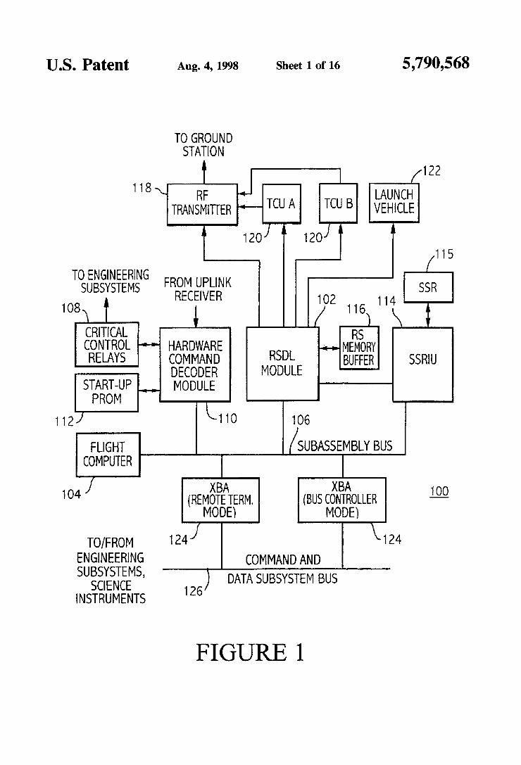
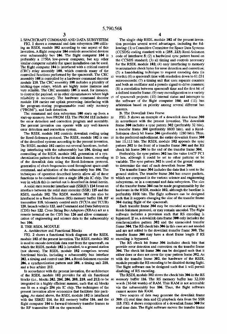
I. SPACECRAFT COMMAND AND D N A SUBSYSTEM The single chip RSDL module 102 of the present inven- FIG. 1 shows a command and data subsystem 100 utiliz- tion provides several novel advantages. including the fol-
ing an RSDL module 102 according to one aspect of this lowing: (1) a Consultive Committee for Space Data Systems invention. A flight COrnpUter 104 controls associated devices (CCSDS) coding standard with a (255.223) Reed-Solomon Over subassembly bus 106- The flight COmPutH 104 is 5 code of interleave 5; (2) a hardwired sync pattern based on Preferably a 175oA 1ow-POwer computer- but any other the CCSDS standard, (3) all timing and controls necessary similar computer suitable for space can be used for the RSDL module 10% (4) easy intdacing to memory The to accumul& check bytes for emor detection and correction; (cRc) assembly lo8+ which Of the ( 5 ) a handshaking technique to request encoding data (in
104 is interfaced with a d k d control
functions performed by the spacecraft‘ The io words); (6) a spaceaaft time with resolution down to 61.03 1 counters
and both an oscillator and a pseudo signal to drive counters; module 110. The CRC assembly 108 includes a plurality of latching-type relays, which are highly noise immune and very reliable. The CRC assembly 1011 is used, for instance, (8 ) a correlation spacecraft time and the first bit Of
to control the payload or in other & c m b c e s where high a defined transfer frame; (9) easy reconfiguration to a variety reliability is necessq. The hardware command decoder 15 Of spacecraft projects; (10) internal status and intempts to module 110 carries out uplink processing. interfacing with the software of the flight computer 104; and (11) bus the program-storing programmable read only memory among Several merent bus (“FROM), and fault detection. masters.
The command and data subsystem 100 starts up from a B. The Downlink Data Frame start-up memory, here PROM 112, The PROM 112 includes 20 FIG. 3 shows an example of a downlink data frame 300 the error detection and correction program and assembly. in accordance with the present invention. The downlink The present invention can operate with any well-known frame 300 includes a sync pattern 302 (preferably 32 bits), error detection and correction system. a transfer frame 304 @referably 8800 bits), and a Reed-
The RSDL module 102 controls downlink coding using Solomon check bit frame 306 @referably 1280 bits). Thus. the Reed-Solomon protocol. The RSDL module 102 is one 2s in the preferred embodiment. the entire downlink frame 308 of the described systems according to the present invention. has 10,112 bits. The RSDL module 102 appends the sync The RSDL module 102 carries out several functions, includ- pattern 302 to the front of a transfer frame 304 and the RS ing: interfacing with the subassembly bus 106, timing and check bit frame 306 to the end of the transfer frame 304. controlling of the RSDL module 102, generation of a syn- Preferably, the sync pattern 302 has the value lACF FC1 chronization pattern for the downlink data frames. encoding 30 D hex. although it could be set to other patterns or be of the downlink data using the Reed-Solomon protocol. variable. The sync pattern 302 is used at the ground station generation of clock frequencies used throughout space-craft to determine the start of each downlink frame 300. command, and arbitration of the subassembly bus 106. The The transfer frame 304 includes the data that is sent to the techniques of operation described herein allow all of these ground station. The transfer frame 304 has source packets, functions to be combined into a single 256 pin IC chip. The 3s which are composed in the various science and engineering way in which t h i s is carried out is described in detail herein. subsystems. or in a command and data subsystem. The size
A solid state recorder interface unit (SSRlU) 114 forms an of the transfer frame 304 can be made programmable by the interface between the solid state recorder (SSR) 115 and the hardware in the RSDL module 102. although the baseline is RSDL module 102. The RSDL module 102 can also be preferably 8800 bits. The flight software can be designed interfaced to a Reed-Solomon (RS) memory buffer 116. RF 40 such that it supports changing the size of the transfer frame transmitter 118. telemetry control units (TCUA and TCUB) 304 during flight of the spaceaaft. 120. launch vehicle 122. and Command and Data Subsystem Each transfer frame 304 may be encoded according to a (CDS) bus 122. Cross String Bus Adaptors W A S ) act as a Reed-Solomon protocol, or may remain uncoded The flight remote tenninal on the CDS bus 126 and allow communi- software includes a provision such that RS encoding is cation of engineering and science data to the subassembly 45 bypassed. If so, a downlink data frame 300 only includes the bus 106. synchronization pattern 302 and the unencoded transfer II. THE RSDL MODULE frame 304. The RS check bits 306 in this case are not needed
A. Architectut and Functional Blocks and are not added to the downlink transfer frame 300. The FIG. 2 shows a functional block diagram of the RSDL transfer frame 304 may have a shod frame length if RS
module le2 of the present invention. The RSDL module 102 M encoding is bypassed. is used to encode downlink data sent from the spacecraft. on The RS check bit frame 306 includes check bits that which the RSDL module 102 is installed. to a ground station provide error detection and correction on the transfer frame (not shown). The RSDL module 102 comprises several 304. The check bit frame 306 can be designed such that it functional blocks, including a subassembly bus interface either does or does not cover the sync pattern frame 302. As 202, a timing and control unit u)4, a Reed-Solomon encoder 55 with the transfer frame 302, the hardware of the RSDL 206. a synchronization pattern unit 208. a timing unit 210. module permits the RS encoding to be disabled during flight. and a bus arbiter 212. The flight software can be. designed such that it will permit
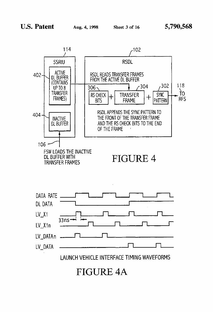
In accordance with the present invention, the architecture disabling of RS encoding. of the RSDL module 102 provides far all six functional The RSDL module 102 stores the check bits 306 in the RS blwks (Le.. blocks 202,204.206,u)8.210, and 212) to be 60 memory buffer 116. The RS memory buffer has 32.000 integrated in a highly efficient manner, such that all blocks words (16-bit words) of RAM. This FL4M is not accessible can fit on a single 256 pin IC chip. The techniques of the via the subassembly bus 106. Thus, the flight software present invention allow economies that facilitate th is pack- cannot access th is RAM. aging. As stated above, the RSDL module 102 is interfaced Two sources of data may generate the downlink frame with the SSRIU 114. the RS memory buffer 116, and the 6s 300: (1) real time data and (2) playback data from the SSR flight computer 104 to forward telemetry transfer frames to 115. FIG. 4 shows composition of a downlink frame 300 for the RF transmitter 118 on the spacecraft. real time data. The flight software moves the transfer frame
assembly 108 is comolled by a hardware co-d &coder dcrosecon&; (7) a timing unit that
arbitration based on
5,790,568 5
304 into a downlink buffer 402 in the SSRIU 114 via the subassembly bus 106. The flight software programs the SSRIU 114 such that the downlink buffer 402 is filled with playback data from the SSR 115. The RSDL module 102 first sends the sync pattern to the TCUs 120 at the start of a downlink frame 300. The RSDL module 102 then reads the transfer frame from the SSRIU 114 and sends it to the TCUs 120. The RSDL module 102 calculates the RS check bits 306 and accumulates them in the RS memory b d e r 116 as the transfer frame 304 passes through the RSDL module 102. The RSDL module 102 sends the RS check bits 306 to the TCUs 120 at the end of the transfer frame 304.
The SSRIU 114 may include at least two downlink buffers 402.404. One of the buffers will be active at any time. For example, if downlink buffer 402 is active, RSDL module 102 reads transfer frames 304 from downlink buffer 402. Downlink buffer 404 is inactive at this time. allowing the flight software to load downlink buffer 404 with transfer frames. The active downlink buffer may contain up to, for example, 8 transfer frames.
The downlink data rate is programmable. This is described in detail below. Preferably, the maximum down- link data rate is 249 Kbps, and the minimum is 5 bps.
The downlink data frame 300 and the clock signal, which is six times that of the data rate clock. are sent to both TCUs 120. The TCUs 120 select which data and which clock signal to use. The downlink data frame 300 is changed at the falling edge of the clock signal.
The downlink data frame 300 and the data rate clock are sent to the RF transmitter 118 along with two additional signals. The first such signal is the real-time interrupt 0 signal. The second signal is the dead period (DEADP) signal. Both of these signals are described in detail below. Here, the downlink data frame 300 is changed at the rising edge of the data clock
The downlink data frame 300 and the data rate clock are sent to the launch vehicle 122. AU signals going to the launch vehicle interface have a 4 12 MHz-cycle pulse width (~334 ns) and have the waveforms shown in FIG. 4A.
C. Functional Blocks The following is a description of the functions performed
by the functional blocks (shown in FIG. 2) contained in the RSDL module 102. Additional discussion of the functional blocks is provided below in the “operation” section.
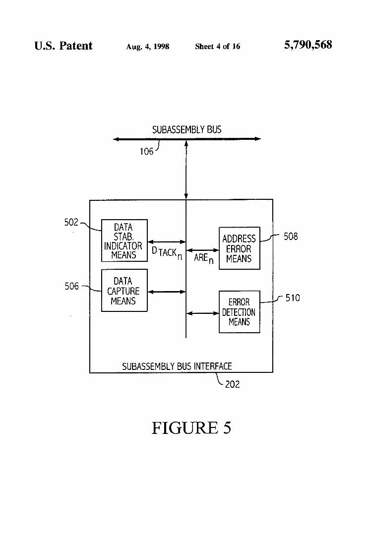
1. Subassembly Bus Interface Block The flight software interfaces with the RSDL module 102
through the subassembly bus interface 202. AU readwrite functions within the RSDLmodule 102 are controlled by the flight software and are performed through the subassembly bus interface 202. The subassembly bus interface 202 also provides interfacing with the flight computer 104 andor the XBAs 124.
The subassembly bus interface 202 also generates a signal indicating when the RSDL module 102 has successfully performed read and write functions. FIG. 5 shows that a stable data indicator 502 determines and indicates whether data is stable during a write cycle at the data pins on the RSDL module 102 by asserting a data transfer acknowledge (DTACKn) signal. The DTACKn signal indicates that data transfer is complete. A data capture device 506 ass- a DTACKn signal during a write cycle when data written by the RSDL module 102 has been correctly captured.
The subassembly bus interface 202 also includes an address mor device 508. Preferably, 256 data registers are reserved for the RSDL module 102. only 14 of which are used. (The data registers of the RSDL module 102 are
6 described in further detail below.) When the subassembly bus 106 references an undefined address from among the 256 registers (i.e.. an address other than one of the 14 registers that are used). the address error device 508 gener-
5 ates an Address Range Error (AREn) interrupt signal. This signal. in turn. sets Bit 9 of the RSDL Interrupt Register (Register 1. described below) to logic level 1, and an RSDL Interrupt (RSDLJNTn) signal is generated No DTACKn signal is returned when an ARFh signal is asserted. because
io the AREn signal indicates that data transfer is not completed. The subassembly bus interface 202 also includes a parity
error detector 510. The parity error detector 510 checks odd data parity on a write cycle. A write operation is inhibited if a parity error occurs. Both the DTACKn signal and a Data
15 Parity Error (DPEn) signal are asserted when a data parity error occurs. In addition, the RSDLJNl’n signal is asserted when a data parity error occurs, and Bit 8 of the RSDL Interrupt Register is set to logic level 1. The parity error detector 510 can also check data parity bits before a write
FIGS. 5A-5D show read and write protocols for the subassembly bus interface 202. The protocol for the subas- sembly bus interface 202 read and write cycles. with no errors, are shown in FIGS. 5A and 5B. respectively. The
25 protocol for the subassembly bus interface 202 write cycle. with data parity error, is shown in FIG. 5C. The protocol for the subassembly bus interface 202 readwrite cycles, address range error, is shown in FIG. 5D.
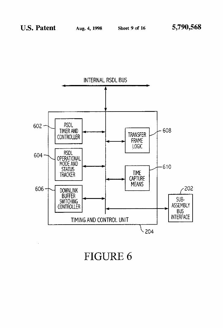
2. Timing and Control Unit
The RSDL module 102 also includes a timing and control unit 204, which is illustrated in greater detail in FIG. 6. The timing and control unit 204 includes a timing and control
35 generator 602 for generating timing and control for the RSDL module 102. The timing and control unit 204 also includes a mode and status device 604 for keeping track of the operational mode and status of the RSDL module 102. The timing and control unit 204 further includes a controller 606 for controlling switching between downlink data buffers 402.404. Finally, the timing and control unit 204 has logic 608 for forcing transfer frames 304 to synchronize with a specified Realtime Interrupt ( F S h ) signal and to use a specified downlink data buffer when synchronization occurs.
The timing and control unit 204 also has a time detector 610 for capturing a time when the first frame of a downlink data buffer 402.404 is output by the RSDL module 102. This time is captured as follows. The Frame Start Register
50 (Register 10) of the RSDL module 102 captures the exact time whenever the first bit of the first frame of a downlink buffer 402,404 is sent out from the RSDL module 102. The relationship between (1) a Power On Reset (PORn) signal and Software Reset (SWRSTn) signal and (2) a First Frame
55 Stamp Capture (FST-CAP) signal is shown in FIG. 7A. The relationship between FtTh and FST-CAP is shown in FIG. 7B. The first bit of the first downlink data frame (Le.. frame start time) output by the RSDL module 102 is valid 6 to 7 clock cycles (approximately 500 to 586 nanoseconds) after
60 reset. The frame start time is valid 6 clock cycles (approximately 500 ns) after RTIn is asserted
3. Reed-Solomon Encoder Block The RSDL module 102 further includes a Reed-Solomon
65 encoder block 206. The RS encoder block 206 includes an RS encoder, which is based on the design of E. R. Berlekamp. in known fashion. The code used in the RSDL
20 cycle.
30
45 (The RTIn signal is explained in detail below.)

5,790,568 7
module 102 of the present invention is defined as (255,233) code with interleave depth of 5. This code is well-known and defined by the CCSDS standard. Those skilled in the art will recognize that other codes and interleave depths could alternatively be employed.
The RS encoder block 2.06 also includes a multiplexer for selecting input from either a clock in the synchronization pattern block 208 or the S S W 114. The RS encoder block 246 interfaces directly with the RS memory buffer 116 with internal addresses. In addition. the RS encoder block 206 has the capability to bypass RS encoding when the flight soft- ware specifies.
The RS encoder block 2.06 requires only 128 words of RAM to calculate the RS check bits 306. The RS memory buffer 116 (i.e.. the RAM accessed by the RS encoder 206) has 32.000 16-bit words of data storage. The lower 8 k of the RAM is broken up into 64 segments, with 128 words/ segment, rather than not using most of the RAM. Only one segment is used if no cell failures occur within the RS memory buffer 116. The RSDL module 102 can be pro- grammed to use a different segment of RAM. however, if a cell does fail in the RS memory buffer 116.
As stated above. RS encoding can be turned on and off. The RS check bits 306 are generated when RS encoding is turned on and are appended to the end of each downlink data frame 300. A downlink data frame 300 is smaller by 1280 bits when RS encoding is turned off. because the RS check bits 302 are not generated and appended to the frame 300.
4. Synchronization Pattern Block
The synchronization pattern block 24U3 of the RSDL module 102 is preferably hardwired logic for generating a fixed hexadecimal synchronization pattern. The preferred fixed synchronization pattern is lACFFClD hex.
It should be recognized. however. that the synchroniza- tion pattern unit 208 could alternatively be software or a combination of hardware and software. Further. the synchrc- nization pattern unit 208 could be designed such that it generates various or selected synchronization patterns, rather than a fixed pattern, where the pattern is varied or selected depending on a variety of factors. In the preferred embodiment. the synchronization pattern unit 208 is designed such that it is controlled by the timing and conlrol unit u)4. It is also designed to receive data from downlink buffers 402.404 and to shift the synchronization data out serially for every downlink frame. starting with the most significant bit (MSB). to the RS encoder block 206.
5. T i g Unit
The timing unit 210 generates clock ffequencies used throughout the command and data subsystem 100. FIG. 8 shows that the timing unit 210 is divided into three sections: fixed T i i g Chain (TC) section 802. Spacecraft Time (SCrime) section 804. and Downlink Frequency Generator (DLGen) section 806.
The TC section 802 converts the system clock of 11.944. 800 Hertz into most of the frequencies needed for the command and data subsystem 100. AU frequencies gener- ated by the TC section 802 are derived from a fixed timing chain.
FIG. 9 shows the blocks comprising the TC section 802. including a 11,944.800 Hz oscillator 902 and counters 904. 906,908,910. FIG. 9 also shows how the elements of the TC section 902 interface with the Sflime section 904. The first counter 904 receives the timing signal from the oscillator
8 902 and divides that signal by 2360. The first counter 902 then outputs a relay signal of 2048.148 Hz, with a 1.004 ps pulse width, which is used by the CRC assembly 108. The second counter 906 receives the timing signal from the
5 oscillator 902 and divides that signal by 27. That divided signal is output to the third counter 908, which then divides by 13825. The third counter 908 then outputs the resultant 32 Hz signal to the S f f h e section 804. which uses this signal internally. The SCI’ime section 804 includes a 37 bit counter 912, which outputs an SCTime signal. as shown.
The fourth counter 910 also receives the timing signal from the oscillator 902 and divides that signal by 27 or 28. The fourth counter 910 divides by 27 for 511 ns pulses and by 28 for the 5 12 ns pulse. ( T h i s will be described in further detail below.) The fourth counter 910 then outputs the
l5 divided signal (a 16,384 Hz pseudo signal) to a 9 bit counter 912 in the SCTime section 804. The 9 bit counter 914 then outputs a higher resolution Sflime signal, as shown. This higher resolution time signal provides 9 additional bits of spacecraft time resolution over the spacecraft time signal
2o generated by the 37 bit counter 912. In th is case, the 9 bit counter 914 outputs subseconds. Counter 914 also outputs an Engineering Flight Computer timing signal of 64.00462 Hz, with a pulse width of 1.004 ps.
The SOime section 804 contains the counters and reg- isters used to set and read the Spacecraft clock, to record the frame start time. and to generate the ARTI, Zrrz and DEADP signals (which will be desrsibed further below). The frame start time means the time of the first frame of every downlink buffer.
The spacecraft clock is functionally a 46 bit counter. which comprises the combination of the 37 bit counter 910 and the 9 bit counter 912. The spacecraft clock keeps track of time from 0 to 4,294,967.295.999 seconds
35 (approximately 136 years) in 61.031 ps intervals. The space- craft counter is preferably never reset. It retains its previous value after a warm boot. It contains a random value after a cold boot (power-up). The time format is split into three 16 bit words. Two of the three words represent the number of
4o elapsed seconds (“second elapsed words”). while the third word holds the elapsed subsecond count (“subsecond elapsed word”). Only the most significant 14 bits of the subsecond elapsed word are used, with the two least sig- nificant bits being permanently set to logic 0. These space-
45 craft time words are mapped to Registers 7, 8, and 9 (described below) of the RSDL module 102.
The actual value of the spacecraft time counters are driven directly onto the subassembly bus 106 when either of the second elapsed words is read. The value of the counter is
so loaded into a bufFer register (“subsecond b d e r register”). which prevents the subsecond bits from transitioning during a read cycle. The subsecond buffer register is loaded continuously, except during a subsecond elapsed word read when the loading of the subsecond buffer register is dis-
55 abled Thus, the spacecraft subsecond t h e is obtained exactly at the beginning of the memory read cycle of the subsecond buffer register.
The subsecond elapsed word is also loaded into a separate frame start register when signaled by the RSDL module 102.
60 This register al lows the RSDL hardware to record the start time of the first frame of every downlink buffer 402.404. This value does not change until the downlink buffer is switched from one buffer (e.g.. downlink buffer 402) to the other (e.&. downlink buffer 404). The frame start register is
The Sffime section 804 also generates the RTIn. ARTIn, and DEADP signals. These signals are derived directly from
lo
25
30
65 read by the flight software.
5,790.568 9 10
the spacecraft clock. The FTIn signal (the real time intenupt reserved for the RSDL module 102. Register 1020 (i.e., signal) is derived from the 0 to 1 and 1 to 0 transitions of the Register 7) contains the 16 MSBs of spacecraft time. Reg- >’& second bit in the spacecraft clock. Thus. KI% occurs at ister 1022 (i.e.. Register 8) contains the middle 16 bits. a rate of 8 per second. The RTIn signal is connected to a Register 1024 (i.e- Register 9) contains the 14 UBs. The Software Interrupt input on a fault detection unit, which is 5 two LSBS in register 1024 (Bits 14 and 15) are always set to
of the hardware command decoder module 110. ne logic level “0”. Registers 1020 and 1022 contain bits rep-
signal to be asserted by the flight computer 104 when RTln is left unmasked. mis produces an intmpt the flight computer The cause of the intempt can be determined via the flight software and registers in the flight computer
is derived from the spacecraft time counter and occurs approximately 5 ms before the KI’I signal. Both the RTln and AIzTIn signals have approximately a 1.004 ps pulse 15 width. The DEADP signal (dead period signal) is the time between the end of the AIMl signal and the beginning of the
occurrence of causes the subassembly bus interrupt resenting the elapsed seconds of spacecraft time. Regster contains subseconds.
Preferably, only 32 of the 46 bits of spacecraft clock time are loaded. That is, the spacecraft time is only loadable to a 1 second resolution. The two word spacecraft time is loaded into holding registers and is transferred to the actual space
for loading the timing unit 210 are given in the tntth table:
‘04‘ The signal (the asynchronous real the craft clock when time load are met. Conations
TABLE 1
SIC T m is KIT signal. The DEADP signal is active from the end of the Redlmdant Groundup- pulse to the beginning of the RTIn pulse. Shmg dateEn- Lmdd at PRIME Health abled TU-SWI’LEN Next
Preferably, the flight software performs three read cycles 20 to read the spacecraft time. The three word value of space craft time read by the flight software may be corrupted if RTIO happens at any time during these read cycles. The flight software can handle prevention andlor detection of spacecraft time corruption. Further. the flight software can prevent spacecraft time corruption by ensuring that KTIO never occurs during the three word read of spacecraft time.
Another counter can be driven by a power-of-two fre- quency higher than 32 Hz in order to resolve times under !/3Z second. A frequency is generated by counter 910 that is a pseudo 16,384 Hz signal. because no such frequency can be directly derived from the 11,944,800 Hz oscfitor 902. This pseudo signal toggles exactly 512 times over a y32 second time period (i.e., 16384 times per second). Another 9 binary bits of spacecraft time resolution (in t h i s case subseconds) can be obtained by using the pseudo signal to drive a separate counter 914. The period of one of the 512 ns time pulses is longer than the rest by a factor of 28/27 to achieve this pseudo 16,384 Hz signal. (See the fourth counter 908 in FIG. 9 and description above.)
true don’t care h e trut RTI false tnw don’tcare true XRTI false falsc InE true RTI
25 Table 1 shows two timing signals. RTIn and XIZTIn, that can be used to initiate spacecraft time loading. The RTIn signal is generated in the timing unit 210 and allows the time to be loaded on a second boundary (assuming software only allows a load on RTI 0). The XRTIn signal is a cross-
30 strapped RTI that is generated in the XBA 124. The XFtTIn signal is broadcast to a secondary command and data subsystem (CDS) string from a prime CDS string and allows a secondary timing unit to synchronize its time to the primary timing unit 210.
The PRIME and Ground Update Enable inputs are -ti- cal Controller (CRC) bits. The PRIME signal indicates whether the CDS string is a primary or secondary CDS string. The PRIME signal comes from the hardware com- mand decoder module 110. The Ground Update Enable signal is used to indicate if the ground wants to update spacecraft time. The Ground Update Enable signal must be set before and cleared after each new time is loaded, if the signal is being used to allow loading of a new time. Multiple ground directed loads will not occur by leaving the Ground
me Redundant string ~ ~ a l t h (RS-TH) signal comes from the hardware command decoder 110 and reports on the
CDS string health. ne TU-S- bit is Bit 4 in the R ~ D L Status and T * ~ Unit conhi ~ ~ g i ~ m
unit 210 to load the 32 M S B ~ of spacecraft time. TU-S- bit is set by software to allow a new time to be loaded. assuming all other conditions are met. The TU-SWTLEN bit is automatically cleared when the space-
35
One of the counter transitions Will represent a longer h e interVal thm Other transitions. This is beCaUSe the pseudo 16384 HZ signal is being used to force the transitions of the least Significant bit (UB) Of a counter. and because one Of 45 Update Enable bit set. these 5 12 ns pulses has a longer period than the other pulses. The b e elapsed is aWo-*b 63.291 PS when the 9 bit counter 912 transitions from 00000001 to OOOOOOO1O. Every other transition. however. occurs at an interval of
count to be accurate (because 512 transitions equals exactly 1/32 second) and deterministic for time measurements under 1/32 second FIG. 1OA shows how the 37 bit counter 910 and the 9 bit
counter 914 are used to produce the 46 bit spaceaaft time. 55 craft time is actually loaded The upper 32 bits Of spacecraft time (i.e.. the second count The new meword spacecraft time is loaded into the bits) are held in the 32 MSBs of the 37 bit counter 912, upper 32 bits ofthe which is clocked by the 32 Hz timing signal. The upper 5 when the timing unit 210 is in the RIME and the bits of subsecond spacecraft time are held in the 5 LSBS Of mound Update Enable and TU-SWTLEN bits are set. If the 37 bit counter 912. The nine next highest bits Of 60 timing unit 210 is secondary. if the R S m W is asserted, subsecond spacecraft time are held in the 9 bit counter 914, and if the TU-SWTLEN bit is set, then the new two-word Which is clocked by the 16,385.185 Hz signal. The two B B s space craft time is loaded into the upper 32 bits of the 1002 Of spacecraft time, as explained above. are set to logic spacecraft clock counter and all sub-second bits are cleared 0. at the next occurrence of XTRIn. This allows for synchro- mG. 10B shows three registers 1020. 1022. 1024 into 65 nization of the secondary with the prime C D S string. This
which the &-bit spacecraft time can be mapped Preferably, result will occur regardless of the state of the Ground Update these are Registers 7, 8, and 9 of the 256 data registers Enable bit.
~ P r O ~ t e l Y 61.030 PS. This d O W S for the subsecond (Register 0). me T U - S ~ bit is used in the timing
block canter at the next

5.790,568 11 12
If. on the other hand. timing unit 210 is secondary. but the Those skilled in the art will recognize, however. that the bus RSHEALTH signal is not asserted. and if the Ground Update arbiter 212 can be designed such that it provides bus Enable and TU-SWTLEN bits are set, then the new two- arbiQation for greater or fewer than four bus masters. word spaceaaft time is loaded into the upper 32 bits of the Four bus request lines (BRkBR3) are used to request SPaceaaft Clock counter at the next-. This allows for the 5 access to the subassembly bus 106. Each bus request line pound to load the ‘Om the pound when the corresponds to a possible bus master. BRO has the highest
priority, while BR3 has the lowest priority. Corresponding prime CDS string is bad. The DLGen section 806 genates the downlink Output bus grant lines (BWBG3) are used to grant access to the
subassembly bus 106. The bus request and bus grant fines
The following sequence of events defines how a bus master achieves and maintains access to the bus 106 from
request signal. The bus arbiter 212 then asserts the corre-
of the subassembly bus 106 until it deasserts its request
signal (DLom)* D L o W is divided by 12 to ob& a downlink data rate signal. This x12 signal is used in gen- io are prefaably active in a low logic state.
the downlink &ta transmission rate. The DU;en ‘06 has both a fixed and a downlink
a and sets a downlink data transmission late Of
allows selection of downlink data transmission rates from 5
data rate+ The fixed data rate is the flight computer 104. A bus master first a s s a s its bus
(bPs)‘ The programmable data rate Option l5 sponding bus grant line. The bus master is then given control bits Per
to 248.850 bps to DLouT frequencies Of 6o signal or is signaled to exit the subassembly bus 106 by a bus to 2.986.200 bps). The selection of a fixed or F o g r m b l e by the bus &,iter 212. data rate is controlled by a downlink data rate select bit ( D U S ~ ) , is ~i~ 5 in the RSDL status and control 2o Register (Register 0). FIG. 11 shows the DLGEN section 806 in greater detail.
me DLGen section 806 is coupled to an internal bus 1102
16-bit bus. as shown. The internal bus 1102 is coupled to a 25 2-bit preload register 1104 and a 16-bit preload register 1106. The internal bus 1202 inputs data into those two registers 1104. 1106. The two registers 1 1 ~ , 1 1 ~ , are. in turn. coupled to an 18-bit counterload register 1108. Regis- krs 1104. 1106 input the programmable 18-bit counterload register 1108. The DLGen section 806 also includes hardwired logic 1110 for setting the default downlink data transmission rate of 5 bps. An 18-bit multi- plexer 1112 multiplexes between the 18-bit counterload register 11841 and the hardwired logic 1110, depending on the 35 master makes an access D ~ S E L simal. ~ a d g ~ , the l&bit multiplexer 1112 is used to select either the programmable data rate the fixed
rate of 5 bps. The 18-bit multiplexer 1112 inputs the
The bus arbiter 212 has two distinct modes of operation. The first mode describes the arbitration of the subassembly bus 106 between the four bus masters under n d OF- ating conditions. T h i s first mode is referred to as the “normal mode.” The second mode describes the “arbitration” of only
mode.” The hog mode is only active when a ,,hog line,,
mode assigns *e highest priority for bus to the flight C0mPUter 104* second P r i d q to the
into the 30 XBAS 124. and thhd and folnth priorities to undefined bus masters. ACmr&n@Y, the bus arbiter 212 eVlOYs a S m l e Prio*v mechanism in the mode *at grants bus ownership to the highest priority bus master. Ownership of the SUbSSed1Y bus 106 Will not change unless another bus
m e flight comPum IO4 can hold the subassembly bus 106 as long as necessary. because it has the highest @ofiq- The flight Computer 104 Only loses control of bus 106 when it deasserts. AU other bus masters
in the RSDL module lo2* me bus ‘lo2 be a the =A bus master. This second mode is refared to as the
is asserted The
selected data rate into an Il-bit lm&ble counter 1114, which is timed by the 11.944.800 H~ signal.
are allowed to hold the subassembly bus 106 until they are timing 40 forced off. This occurs when a bus request signal from
another bus master is received by the bus arbiter 212. The bus arbiter 212 issues a bus abort signal when it receives a bus request. The bus arbiter 212 then grants bus access to the
preferably, the DLan section 806 is implemented as a &,ider. ms design takes the loadable
11,944.800 Hz system frequency and &vides it to the x12 that frequency used by the RSDL module 102. The frequency 45 was deasserted and the bus master requesting control Of the
higher Moriv bus between the Mor bus
divider is an 18-bit wide counter 1114 that is loaded from the subassembly bus downlink preload registers 1104. 1106. The divided value The bus arbiter 212 grantS access in the hog mode O d Y to will be transferred from the preload registers to the downlink the bus master 124. All Other bus master requests are rate counter 1114 at the next Kl’In signal by setting the not recognized bY the bus ad~iter 212. preferably+ the hog downlink rate load bit (Bit 6) in the RSDL Status and 50 mode is used only for support equipment access to the Control Register (Register 0). subassembly bus 106 before launch of the spacecraft. Thus.
the bus arbiter 212 forces all other bus masters off the subassembly bus 106 in the hog mode and assigns exclusive
The bus arbiter block 212 provides lo& to control the use of the subassembly bus 106 to the second priority bus subassembly bus 106 and generates control signals to enable 55 master, here the XBA controller 124. a 2A2 Board Address Bus. FIG. 12 shows a timing diagram IU. THE RSDL MODULE DMA REGISTERS for the bus control signals. BG is the bus grant signal, which The RSDL module 102 has 256 data registers. The is described below. XBA-ADENn is an address enable registers are numbered from 0 to 255. Each register holds 16 signal for the XBA 124. It enables the 2MBoard Address bits of data (or one data word). The most significant bit Bus when the XBA 124 is bus master. XBA ADDR is the 60 (MSB) of each registex is bit 0. and the least significant bit XBA bus direction signal that controls the 2A2Board (UB) is bit 15. Address Bus direction. The flight computer 104 is the Register 0 is addressed by the least significant address of subassembly bus 106 master if XBA ADDIR is logic level the memory range reserved for the RSDLregisters. Only 14 “1.” The XBA 124 is master is XBA ADDIR is logic level registers are used out of 256 reserved for the RSDL module ‘Y).” 65 102. The AREn signal is asserted when the software wri tes
The bus arbiter 212 performs bus arbitration for the to the unused registers, but no DTACKn is returned to the subassembly bus 106 between four possible bus masters. subassembly bus 106.
6. Bus Arbiter Block

5.790.568 13
Writing to the RSDL registers requires special attention. Most of the registers have a portion of read-only bits, read-write bits, and unused bits. Also, a special bitwrite scheme is used far status, control. mask. and interrupt registers (Registers 0 and 1). The MSB in this special bitwrite scheme has the value to be written to the register. A “1” at all other bits indicates that a bit will be written by the value stored at the MSB. and a “0“ indicates that a bit will remain the same. The following examples illustrate the special bitwrite scheme:
Write to Register i: 1Mx) Do00 1111 1111
Write to Register i: m Do00 1111 1111
Registeribeforewrite: OOM] 1111 oo00 1111 Registeriafterwrite: OOM] 1111 1111 1111
Registcribefore write: oo00 1111 1111 1111 Registeriafterwrite: oo00 1111 OMXI OODD
AU the bits in the RSDL registers are classified as follows: R ordinary read SW Special write scheme W ordinary write U: Unused bits. Read back 0 and write don’t care. Register 0 is the RSDL Status and Control Register. Its
address is 1 EFSOO. hex. AU bits in Register 0 are equal to 0 after reset, except the mask bits. which are set to 1.
0 (USW
1
2
3
4
5
6
I
8
9
10
W
SWiR
swm
swm
sw/5
swm
swm
SWiR
sw/R
swm
swm
Spccial bit. This value will be written to all affected bits. R d i this bit will always give 0 value. Buffer Swap Enable. Flight software sets this bit to enabk the swapping of the downlink bu&m 40% 404. The hardware will clear this bit when tk doMllink buffer swap. Sync WI: flag. A “1” at this bit means that the transfer frame 304 needs to be rcsylrhronizad w h the RTI signal arrives. The Aight software sets the 5ag in r o d operation, and the RSDL hardware msets the fkg when the RTI occurs. Force Buffer bit. The force bu&r (see bit 14) will bscome thc downlink bufk w k n this flag is set and the sync RTIoccurs. ‘N SW’TIEN bit. This bit is used in the tirning unit 210 to load 32 bits into the 32 MSBs of the spacecraft time. This bit is cleared by hardwm after th value has bccll lcaded to the space- craft tim. DLRatc Select bit. This bit is d i n t h e riming unit 210. This bit seltcts which prsde- 6 1 4 value will be used in the DLCb806. DL Rate Load bit. ?his bit is used in the timing unit. whcn this bit is sct and the RTI occurs, the Ww value of th downlinkdatamte will be leaded into thc DLGcn 806. This bit is cleared by the hprdware after the vduc has been loadtd. Dmbled Buffer Swap Mask bit. When this bit is set, the Disabled Buffer Swap Intmvpt signal will be maslrcd. DPEn Interrupt Mask bit. when it is masked, tb DPEn m o r will be saved in the RSDL Interrupt Register (see below) and will assert the Dffin line, but not the RSDL-XNTn Line. A “1” at this bit meam mask out thc corresponding intermpt. AREn Intemtpt Mask bit. when it is masked, the emor will be saved in the RSDL Interrupt Register, and SSRIU 114 will assert th AREn h, but not the RSDLANTn Line. Waf-Buffer Interrupt Mask bit. When masked, this intempt will be saved in the RSDL Iuter- ~ p t Register, and thc RSDL-INTn hne will not bcassertcd
5
10
15
20
25
30
35
40
45
50
55
60
65
14 -continued
Bit # Fme Descriution
11 SW/R Start-of-Buffer Jntemupt Ma& bit. When masked, this mtcrmpt will be saved in the RSDL Inter- rupt Register, and the RSDL-JNTn line will not be a&?erted.
12 R Current DL Buffer ID. 0 selects downlink butrcr 402 ( t h “A” buffer) is selected, and a “1” means that downlink buffer 404 (&e ”B” buffer) is SeleCted. C m n t RS Encoding Status. A “0” at this bit means that the RS encoding is on; othcrwisc RS
DL Fome Buffer ID. A “cy‘ at this bit means that th A buffer 402. When the Buffer flag is set and Sync RTI occurs, bu&r 402 will become the downlink buffer.
will be used when Sync RTI occurs.
13 R
encoding is off. 14 SWlR
15 SWlR Next RS Encoding Status. This encoding status
Register 1 is the RSDL Interrupt Register. The address of Register 1 is 1EF501. hex. The bits in this register are set by hardware and cleared by software. Setting any bits in this register will cause the RSDL interrupt signal (RSDL-INTn) to be raised if the corresponding masking bit (i.e.. Bit 7 of Register 0) is not set. Bit 7 and Bit 11 of Register 1 are set and a l l other bits will be cleared after the PORn signal or the software resets. Software is allowed to set the bits in this register for testing purposes in order to invoke interrupt handler routines directly. This capability should not be used, however, in normal (or non-testing) operation.
Bit# lLpc Description
O(MSB) W Special bit. This valut will be wntten to all affected bits. Hm, only 0 value a&ts the registe.r, Reading of this bit will always give a 0 value.
1-6 U Spare bits. I SWm Disabled Buffer Swap Iutcmpt. This bit is ast
when the downlink bu&r swaps on itself because tbt ButTer Swap Enable bit (Bit 1 of Register 0) is disabled. DPEn intemtpt bit. This bit is set wbcn the software writes to tbe RSDL mxiuk 102 with a data parity error.
9 Local AREn interrupt bit. This bit is set when th sof~~are accesses an undcfinad address.
10 SWm Buffer Overflow Intempt bit. This bit is set when the downlink reads past th end of the dowdhk buffer 402,404. In that case, thc last word of the downlink buffer will always be re- Nmod.
when the downlink buffcr 402,404 swaps to an- other buffer or on itself.
8 SWm
SW/R
11 SWiR Startaf-Buffer interrupt bit. This bit is set
12-15 U Spare bits.
Register 2 is the Current Frame Information Register. The address of Register 2 is 1EF502. hex.
Bit # T@e Description ~ ~ ~~
0 (MSB) U Spare bit. 1-3
4-5 U S p r e bits. 6-15 R Current Fram Length in 16-bit words. These bits
R C-t DL Buffer Size. These bits are equal to 0 (8 frames) after reset.
8n equal to 550 after reset.
5,790,568 16 15
Register 3 is the Next Frame Information Register. The address of Register 3 is 133303, hex.
~~
Bit # IILpe Desriptiion
0 (MSB) U Spare bit. 1-3 W/R Next DL Bu&r Size. These bits will be used
when the &w&& buffers 402,404 are swapped. Thest bits m equal to 0 (8 frames) after n- SI.
4 5 U Spare bits. 6-15 W/R Next Frame Length in 16-bit words. These bits
will be uscd w k n thc swap buffcr occurs. arc equal to 550 after nmt.
Register 4 is the RS Segment Register. The address of Register 4 is 1EF504, hex. AU bits in Register 4 are equal to 0 after
Bit# 'Qpc Description
0-1 U Spare bits. MSB) 2-7 R clarent Scgmnt Number. This is the segment of
8-9 U Sparebits. 10-15 WIR Next Scgmcnt Number. Tlbzsc bits will be usad
mmorydforRScncoding .
w k n the downlink buffers 402,404 arc swapped
Register 5 is the ScTime Load 1 Register. The address of Register 5 is 1EF505, hex. AU bits in Register 5 are reset after PORn, but remain unchanged after software reset. Register 5 is loaded to the SCl'R2 (Register 8) at FSI boundaries.
Bit# w Desfription
0-15 W/R SC Tm Load 1. Load 16 MSBs of the 8pacccraft thnc.
Register 6 is the SC Time Load 0 Register. The address of Register 6 is 1EH506. hex. All bits in Register 6 are reset after PO-, but remain unchanged after software reset. Register 6 is loaded to the ScTRl (Register 9) at rrn boundaries.
Bit% 'Ifrpc Description
0-15 W/R SC The Load 0. Load 16 mi& bits of the spacecraft timc.
Register 7 is the SC Time Read 2 Register. The address of Register 7 is 1EF507, hex. Register 7 can be loaded by software, but not reset by PORn or software reset.
Bit# Qpc Description
0-15 R SC Tim Read 2. Read 16 MSBs of the spacecraft t h e .
Register 8 is the SC Time Read 1 Register. The address Register 8 is 1EF508, hex. T h i s register can be loaded by software, but not reset by PORn or software reset.
5
10
15
20
25
30
35
40
45
50
55
60
65
Bit # 'Roc Descriution
0-15 R SC Tm Read 1. Read 16 middle bits of tk spacecroft time.
Register 9 is the SC Time Read 0 Register. The address of Register 9 is 1EF509, hex. This register can be loaded by software, but not reset by PORn or software reset.
Bit# Description
0-15 R SC Trmc Read 0. Rcad 16 LSBs of tbe spaceraft time.
Register 10 is the FS Time Read Register. The address of Register 10 is 1EF50A. hex.
~
Bit# T ) p Description
0-15 R FS T i Read. Read 16 LSBs of the spacecraft thnc at tk start of &first framC in tk downlink bu&r 402,404.
Register 11 is the Downlink (DL) Data Rate 1 Register. The address of Register 11 is 1EF50B. AU bits in Register 11 are reset after PORn, but remain unchanged after soft- ware reset. The downlink data rate in th is register will take effect only at KIT boundaries.
Bit# ?Lpe Description
0-15 W/R DL Data Rate Load 1. The two most signilkant bits of the dwnlink data rate in 2's comple- ment.
Register 12 is the DL Data Rate 0 Register. The address of Register 12 is 1EF5OC. All bits in th is register are reset after FQRn. but remain unchanged after software reset.
Bit# Qp.2 Desalptioo
0-15 WIR DL Data Rate Load 0. 16 LSBs of thc &wnhk data rate m 2's complement.
Register U is the Zero Register. The address of Register 13 is 1EF5OD. hex. This register is used to avoid having the Address Range Error (AREn) signal assert when addressing double words.
Bit # w IkscriptiMl
0-15 R All Os.
IV. SOFTWARE CONSIDFWWION The flight software has the responsibility to ensure that
the time for collecting transfer frames is shorter than the time for sending transfer frames. The RSDL module 102 provides a capability for the flight software to disable the swapping of the downlink buffers 402,484 before the frame collection is completed The flight software can enable or disable downlink buffer swapping by setting Bit 1 of Reg- ister 0. If this bit is set when a buffer swap occurs. the hardware will swap to the new buffer and t h i s bit is subse- quently cleared. Otherwise, the Disabled Buffer Swap Inter-

5,790,568 17 18
rupt will be issued. Bit 7 of the Register 1 will be set. and the hardware will swap to the same buffer (swap on itself). The flight software can also mask the Disable Buffer Swap Interrupt by setting Bit 7 of Register 0 to 1. A Begin Buffer Interrupt will always be issued whenever the downlink buffer pointer points to the beginning of the downlink buffer, regardless of whether the swap has actually occurred.
The RSDL Status and Control and RSDL Interrupt Reg- isters (Registers 0 and 1) use a special write scheme that allows access to individual bits. Writing to these registers requires the special bitwrite scheme. as described above. All internal registers are at the states shown in the
necessary) the number of frames in the downlink buffer 402, 404. the frame size, the segment number. and the downlink data rate.
The RSDL module 102 generates downlink data rates from 5 bps to 24.8850 bps. The timing unit 210 provides an 18-bit up counter to generate a x12 downlink data rate that is used in the RS encoder B6. ms is described in detail above.) Thus, the following parameters are used to obtain a downlink data rate of 11.060 bps:
12 times data rate: 132,720 Divisor: 18-bit 2’s complement:
11,944,800/132,720 = 90 or Ox5A 0x3FpF - Ox5A = Ox3FFA6 following tables after PORn and software reset:
Register Value Description l5 Accordingly, the value to be loaded to Register 11 is 3 hex and to Register 12 is OxFFA6 hex. V. OPEFLUION OF THE RSDL MODULE STATES AFTER PORn
0 W l F O
1 O X o l l O
2 0x0226
3 0x0226
4 OxM)(lO
5,6 OxOOOO
7,8,9 NmRe- setable
10 Nm-Re- setable
11,12 OxODOO
0 x 0 l F O
0x0110
2 0x0226
3 0x0226
4 OxoOM) 5,6 ~ n -
changed 7,8,9 Non-Re-
setable
10 Non-Re- &able
11,12 Un-
changed
Downlink b u k is sct to Buffs A 402, all enable bits m reset, all interrupt masks are on, RSDL module 102 is in en- coding d. (Note: For RSDL, mask bits are turned on when they are set to 1.) ‘Ihe Disabled BuEer Swap Interrupt (Bit 7) and Begin Buffer Iuterrupt (Bit 11) are set and all other intenupts are cleated. Note: this value will change m 0x0130 due to thc end-of-buffcr signal approximately 6 seconds after PORn. N u m k of frames is 8, frame she is 550 Words. Number of frames is 8, frame Size is 550 Words. Segment 0 is used for RS encoding. 32 MSBs of t h e w slwcecrsfttime are cleated after PORn only. 48-bit spacecraft Lime. ‘Ihese registas are loadcd by software and will rot be nset by the PORn. 16 LSBs of thc spacecraft time when the Frame Start occurs. This ngister is loaded by mftware and will not be reset
18-bit downtink data late is cleared and the DL rate is szt to a predesnod value Sbitfs after PORn only.
STP;IES AFER RESET
by tht mRn.
Downlink bufer is set to BuEerA402, all enable bits are resct, all interrupt masks an on, RSDL module 102 is in en- d i n g mode. lhe DisPbled BufBcr Swap Interrupt (Bit 7) and Be& BUeer Interrupt (Bit 11) are set and all other itlterrupts are cleared. Note: this value will change to 0x0130 in kssthan 6 seconds after soft- ware reset based on the current cbwulink late. Number of h u e s is 8, frame size is 550 W d . Number of hmes is 8, frame size is 550 W d . Scgumnt 0 is used for RS d i n g . The c m t m of these registers an not changed after software rest . &-bit spacecraft time. These registers are lo& by software and will mt be resct. 16 ISB bits of the spacecraft time w k n tbe Frame Start occurs. This register is I& by software and will not be reset.
A. Turning RS Encoding On and OB The flight software can determine if RS encoding is
20 turned on or off for a current downlink data frame 300 by reading Bit 13 of Register 0, the RSDL Status and Control Register. This bit provides the current RS encoding status and is read-only. A “0” at Bit 13 indicates that RS encoding is turned on, while a “1” indicates that RS encoding is turned
25 off. Both a cold boot and a warm boot clear this bit to 0. The flight software can turn RS encoding on and off by
writing to Bit E. the RS Encoding Select Bit. of Register 0. Setting the RS Encoding Select Bit to “0” causes RS encoding to be turned on at the next Downlink Frame
30 Resynchronization. (Downlink Frame Resynchronization is discussed in detail below.) Setting the RS Encoding Select Bit to “1” causes RS encoding to be turned off at the next Downlink Frame Resynchronization. Both a cold boot and a warm boot clear this bit to 0.
RS encoding is turned on during normal operation. Thus, both Bits 13 and 15 of Register 0 have the value ‘‘0’’ during normal operation.
35
B. Selecting a Segment of the RS Memory Buffer The flight software can select a segment of the RS
40 memory buffer 116. This is done using Bits 2-7 of Register 4. which indicate the memory segment currently being used. These bits are read-only. The RS memory buffer 116 consists of 64 segments, numbered 0-63. Segment 0 corresponds to RS memory buffer 116 addresses 0-127 decimal, Segment 1
45 corresponds to addresses 128 to 255 decimal. and so on. Both a warm boot and a cold boot clear Bits 2 7 of Register 4 to “0”.
The flight software can specify the number of the next RS memory buffer segment by writing to Bits 10-15 of Register
50 4. The next segment takes effect at the next buffer swap or at the next buffer repeat. Both a cold boot and a warm boot clear these bits to “0.”
The flight software will only change the segment number when memory cell failures occur in the RS memory buffer
55 116. Only the ground station will be able to determine if a memory cell failure has occurred. because the flight software cannot directly access the RS memory buffer 116. and because nothing in the hardware of the RSDL module 102 provides for a check of the RS memory buffer 116. As a
60 result, flight software will only switch to a new RS memory segment in response to a command from the ground station.
The mtcnts of these registers are not changed aher software reset.
preferably, the RSDL module 102 does not use all the memory location in a segment. The information in the unused locations may be used if memory failures occur
After reset. the flight software must resynchronize trans- 65 during ground testing. For example, the RSDL module 102 can be made to use only 80 of the 128 memory locations in a segment. Thus. only locations 0 to 39 and 64 to 103 could
fer frames with the next RTI and mask out unwanted interrupts. The flight software must also redefine (if
5.790,568 19 20
be designated in use for segment 0. Locations 40 to 63 and 104 to 127 would then be unused. The relative locations of the used and unusedportions of memory will be the same for the other segments.
software can specify in the RSDL module 102 the number of downlink data frames in a downlink W e r by writing to Bits 1-3 in the Next Frame Information Register (Register 3). Downlink buffer size is then equal to the number of
C. Initialization of the RS Buffer Memory 5 downlink data frames times the downlink data frame size. The hardware in the RS encoder 206 assumes that the The new downlink buffer size takes effect at the next buffer
segment of the RS memory buffer 116 to be used contains all swap. The flight software can specify in the SSRTU 114 the 0’s at the start of each downlink data frame 300. The RS total size of the downlink buffer 402.404 by setting the start check bits 306 for that frame 300 will be corrupted if the and end address of the downlink buffer 402,404. segment does not contain all 0’s. The RS memory buffer 116 io The downlink buffer 402,404 should be specified to be contains random data after power-up. Only one method the same size in the RSDL module 102 as in the SSRIU 114. exists by which the bits in a segment all get cleared to “0”: E. Buffer Swap Versus Buffer Repeat the RS encoder 116 automatically sets all of the bits in that The flight software can enable or disable downlink buffer one segment of memory to “0“ at the end of a downlink data swapping via the Buffer Swap Enable Bit (Bit 1) in the frame 300 when the RS encoder 106 reads the check bits 306 15 RSDL Status and Control Register (Register 0). The new out of the RS memory buffer 116. buffer is swapped and the buffer swap enable bit is cleared
T h i s has four implications. First. the check bits 306 for the when the Buffer Swap Enable Bit is set to “1” and when the first downlink data frame 300 will be corrupted when power end of the current buffer is reached. The same buffer is is fmt turned on. Check bits for subsequent downlink data repeated beginning at the buffer start address when the frames will be uncorrupted. Second. the new memory seg- 20 Buffer Swap Enable bit is set to “0‘‘ and when the end of the ment is not zeroed out and does not contain random data current buffer is reached. In addition. the Disable Buffer whenever a new segment is selected. Therefore. the first set Swap Interrupt bit (Bit 7 ) of the RSDL Interrupt Register of check bits accumulated in the new memory segment will (Register 1) will be asserted when the same buffer is be corrupted. The check bits 306 for subsequent downlink repeated. data frames will be uncorrupted. Third, a warm boot occurs 25 The Begin Buffer Interrupt bit (Bit 11) in the RSDL asynchronous to RSDL operation. This means that the RSDL Interrupt Register (Register 1) is asserted when either a module 102 will most likely be in the middle of processing buffer swap or buffer repeat occurs and when the buffer a downlink data frame 300 when the warm boot in tmpts pointer points to the start of the buffer. Also, the 16 LSBs of operation. The check bits 306 for the first downlink data the spacecraft time are captured in the Buffer Start Time frame 300 will be corrupted after the warm boot. The check 30 Read Register (Register 10) when either a buffer swap or bits 306 for subsequent downlink data frames 300 will be buffer repeat occurs and when the buffer pointer points to the uncmpted Fourth. flight software ensures that Downlink start of the buffer. Frame Resynchronization (see below) coincides with the The hardware of the RSDL module 102 selects as the end of a downlink frame 300 during normal operation. If the downlink buffer the buffer specified by the DL Force Buffer fiight software forces a Downlink Frame. Resynchronization 35 ID bit (Bit 14) in Register 0, regardless of the value of the in the middle of a downlink data frame. check bits 306 for Buffer Swap Enable bit. This selection is made when the the first downlink data frame after the resynchronization will Force Buffer bit (Bit 3) in Register 0 is “1” and a Downlink be conupted. Check bits for subsequent downlink data Frame Resynchronization occurs. A Disable Buffer Swap frames will be uncompted. Interrupt signal is issued. however, if the Buffer Swap
D. Downlink Data Frame Size and Downlink Buffer 40 Enable bit is not set to “1”. Memory Size F. Downlink Frame Resynchronization
Flight software can set the size of the downlink data frame Downlink Frame Resynchronization is used to ensure that 300. The flight software does th is by selecting the number of the start of a downlink data frame 300 periodically al igns wor& in a downlink data frame 300 by writing to Bits 6-15 precisely with an RTIn signal. This penodic alignment is in the Next Frame Information Register (Register 3). 45 used to support time correlation packets, which are Preferably, however, frame size will always be 550 words described in the following section. (i.e., Bits 6-15 of Register 3=226x). Both a warm boot and FIG. 13 shows that the periodic alignment of the start of a cold boot cause the frame size to be set to 550 words. a downlink data frame with an RTIn defines a downlink
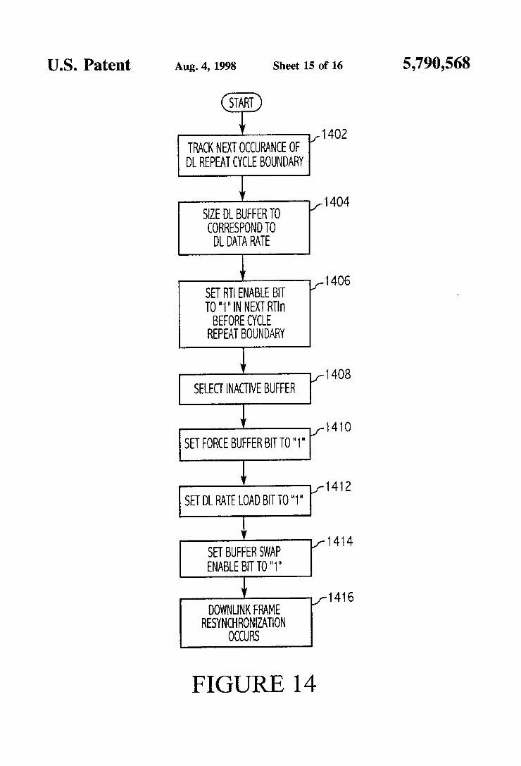
The flight software can also select the size of the downlink repeat cycle boundary. The downlink repeat cycle in FIG. 13 M e r 402.464. The flight software in some cases may use 50 has 512 RTIS per cycle. The flight software should perform a single downlink buffer size the entire time it is operating a Downlink Frame Resynchronization at every downlink at a given downlink data rate. Alternatively, the flight repeat cycle boundary, because of clock drift in the RSDL software can vary the buffer size. l b o criteria exist for hardware and the possibility of the flight software losing choosing the downlink buffer size. First. repeat cycle bound- track of its place in a repeat cycle. Thus, it is important to aries (see FIG. 13) should coincide with the start of a 55 perform Downlink Frame Resynchronization at every repeat downlink buffer. This means that an integer number of cycle boundmy, even thougb the start of a downlink data bder s should exist in the repeat cycle. Second. the buffer frame is automatically aligned with an RTI when Downlink size should be as large as possible and stili meet the first Frame Resynchronization has been performed once. BiteriOn. FIG. 14 is a flow diagram illustrating how the flight
For example, F’IC. 13 shows the repeat cycle for a 60 software perfoms a Downlink Frame Resynchronization at downlink data rate of 248,815 bps. Each transfer frame in every downlink repeat cycle boundary. Flight software first th is case has 10,112 bits. assuming 550 words per frame, and (Step 1402) keeps track of when the next downlink repeat assuming that RS encoding is turned on. The repeat cycle is cycle boundary will occur after a Downlink Frame Resyn- 512 FCl% per downlinkrepeat cycle. In consequence, exactly chronization. Preferably, the flight software does th is by 225 buffers of data are sent out for every repeat cycle. 65 counting RTLs. It should be recognized however, that there
The flight software must specify the downlink buffer size are other ways for the flight software to determine when the in both the RSDL module 102 and the SSRIU 114. Flight next downlink repeat cycle boundary will occur.

5,790,568 21 22
Next (Step 1404). flight software sizes the downlink Five conditions exist that can result in the interrupt being buffer 402.404 for a given downlink data rate. such that the asserted within the RSDL module 102. The occurrence of start of a buffer coincides with the repeat cycle boundary. any one of these five conditions sets one of Bits 7-11 in the The flight software then sets the Sync RTI Enable bit in RSDL Interrupt Register (Register 1): Bit 7, Bit 8, Bit 9. Bit Register 0 to a “1” (Step 1406) in the next RTI before the 5 10. or Bit 11. The meaning of each of these bits is described upcoming Cycle Weat b0un-e step 1404 forces a Down- in detail above. A mask bit corresponds to each of these link Frame Resynchronization to occur at the next F3.L interrupt bits. The mask bits are contained in Bits 7-11 of
then sets to “l” the DL Force Buffer Register 0. Those bits correspond to Bits 7-11 of Register 1. ID bit in Register 0 to select the inactive buffer (Step 1408). interrupt which should be full of downlink transfer frames. The Force 1o bit is masked when the mask bit is set to ,,l,,. Buffer bit io Register 0 is also set to a “1” (Step 1410). This HG. 15 shows that the five interrupt bits are logically is done so that the buffer specified by the DL Force Buffer ANDed with the inverted mask bit and then ID bit will be used at the next RTI. The DL Rate Load bit in Register is then set to ‘619v d ~ n g the RTI period (step logically ORed together to produce the interrupt. In 1412). mis allows the RSDL hardware to the consequence, an intermpt bit remains set to “1” until the Downlink Frame Resynchronization smoothly. 15 flight software clears it. The RSDL interrupt is asserted
The flight software then sets the Buffer Swap Enable bit where all Of the interrupt bits are Unmasked and if one Or in Register 0 to a +‘1” (Step 1414). This is done to prevent more of the interrupt bits are set to a “1”. The flight Software the Disable Buffem Swap Interrupt bit in Register 1 from must reset all of the interrupt bits to 0 for the RSDL interrupt being asserted. Finally. the Downlink Frame Resynchroni- to clear. zation occurs (Step 1416). and the buffer specified by the DL 20 Although only a few embodiments have been described in Force Buffer ID bit is used at the next RTI. detail above. those having ordinary skill in the art will
The RSDL hardware performs a Downlink Frame Resyn- readily realize that many modifications are possible without Chrollhtion With no loss Of data if the resynchronization departing from the advantageous teaching therein. For occurs at a downlink repeat cycle boundarv. N O downlink example. a hardware embodiment has been described above frames will be comPted, however+ if the flight software 25 for carrying out various functions. Many advantages of the forces a Downlink Frame Resynchronization in the middle present invention are obtained from the hardware operation. Of the rept cyc1e* In this case* the downlink data frame However it should be understood by those having ordinary prior to the resynchronization is terminated in the middle, skill in the art that certain of these advantages and functions and the RS check bits 306 in the downlink data frame 300 can also be carried out in
programmed with firmware to carry out the functions of this sequent frames. however. will be uncmpted
assembly. It should be understood that these systems are not clock by using a ~ i m ~ Correlation packet. ne ~h~ cor- limited therefore, to hardware. Other similar modifications relation Packet is sent to the ground station Once every would also be apparent to those having ordinary skiU in the downlink repeat cycle. A ~h~ Correlation Packet a n 35 art. and are intended to be encompassed within the foliowing appear anywhere in the repeat cycle. The Time Correlation C W S . Packet contains the “time.” at which the first bit in the first We claim: downlink data frame 300 in the downlinkrepeat cycle is sent 1. A monolithic Reed-Solomon downlink (RSDL) encod- from the command data subsystem 100 to the RF transmitter ing chip for processing downlink frames to be transmitted 118. Here. the “time” is the spacecraft time. The flight 40 from a spacecraft to a ground station, each downlink frame software obtains th is “time” by reading the 16 LSBs of including a synchronization pattern and a transfer frame, the spacecraft time captured in the Buffer Start Time Read RSDL encoding chip being couplable to first and second Register, by reading the 16 middle bits of spacecraft time data buffers for storing transfer frames and to a data bus, the from the SC Time Read 1 Register (Register 8). and by RSDL encoding chip comprising: reading the 16 MSBs of spacecraft t h e from the sc Time 45 Read 2 Register (Register 7).
The flight holds the bits. The
For example, a are foliowing the resynchronization* A‘ ”b- 30 purpose digital propessor be appropriately
G. Buffer Start Time Correlation me ground station keeps track of drift in the
a, a timing device for maintaining a spacecraft b e and for generating an internal signal for controlling timing of the RSDL encoding chip;
ing the RSDL encoding chip with a plurality of space- craft devices
to the timing device and to the bus interface, for controlling which of the first and second data buffers can communicate transfer frames to the bus interface;
d. a synchronization pattern unit. coupled to the timing and control unit. for generating the synchronization pattern;
e. a Reed-Solomon encoding unit, coupled to the s P - ChrOnization P a e m Unit and to the and control unit, for receiving and encoding the transfer frames according to a Reed-Solomon protocol; and
f. a bus arbiter, coupled to the bus interface. for arbitrating between the plurality of spacecraft devices and granting access to the data bus to one such device at a time.
2. The RSDL encoding chip of claim 1 wherein the Reed-Solomon encoding unit can be enabled and disabled.
The RSDL module 102 captures the 16 LSBs of the
ever it is swapped at the start of either downlink buffer 402, 404. That is, the contents of the Buffer Start Time Read so Register correspond to the time that the first bit in the synchronization pattern 302 in the first downlink data frame 300 associated with the first transfer frame in the buffer is sent to the RF transmitter 118.
that the first bit in fie first downlink data frame the r a d cycle is sent from the command data subsystem 100 to the RF transmitter 118 after a Downlink Frame Resynchroniza- tion. The flight software must read the contents of this register before the next downlink buffer swap or downlink 60 buffer repeat. The RSDL hardware overwrites the contents of this register at the next downlink buffer swap or downlink buffer repeat.
time in the Buffer Time Read Register when- b. a bus interface, couplable to the &ta bus, for interfac-
to the RSDL encoding chip; c. a timing and control unit,
The Buffer Start Time Read Register contains the time 55
H. RSDL Module Intermpts The RSDL module 102 can assert an intermpt on the 65
subassembly bus 106. This interrupt generates a level 12 IOIC channel 3 interrupt in the flight computer 104.

5,790,568 23 24
such that the transfer frame is not encoded according to the Reed-Solomon protocol when the Reed-Solomon encoding unit is disabled and is encoded according to the Reed- Solomon protocol when the Reed-Solomon encoding unit is enabled; and wherein the Reed-Solomon encoding unit is 5 further for generating at least one check bit when the Reed-Solomon encoding unit is enabled, the check bit providing for mor detection and correction on the transfer frame. transfer frame; and
3. The RSDL encoding chip of claim 1 wherein the io synchronization pattern unit comprises hard-wired circuitry for generating the synchronization pattern.
4. The RSDL encoding chip of claim 1 wherein the Reed-Solomon protocol is a (255,223) Reed-Solomon code of interleave 5.
5. The RSDL encoding chip of claim 1 wherein the l5 spacecraft time has a resolution of at least about 50 micro- seconds.
6. The RSDL encoding chip of claim 1 wherein the spacecraft time has a resolution of about 61 microseconds. 7. The RSDL encoding chip of claim 1 wherein the bus 2o
arbitrator has two modes Of operation, a ~~ mode and a hog mode; wherein in the n o d mode the bus arbitrator grants access to the data bus based on a priority scheme, in which each of the plurality of spacecraft devices has a priority designation; and wherein in the hog mode the bus 25 arbitrator grants access exclusive access to the data bus to a predetermined one of the plurality of spacecraft devices.
8. The RSDL encoding chip of claim 1 wherein each
transfer frames is programmable. u1 timing signal has a frequency of 11.944.800 Hz and the
19. The RSDL encoding device of claim 17 wherein one number of transfer frames stored in the first and second data of the pulses is longer than the remainder of the pulses by a buffers is programmable.
10. The RSDL encoding chip of claim 9 wherein the factor Of 28/27*
second data M a s is in a range of 1 to 8. encoding chip for processing downlink frames to be trans-
timing and control ,,nit is f ~ a h e r for generating a downlink including a synchronization pattern and a transfer frame. the data rate. RSDL encoding chip being couplable to first and second
12 me ~ D L chip of 11 the data buffers for storing transfer frames and to a data bus, the downlink data rate is programmable.
13. The RSDL encoding chip of claim 1 wherein a a. a timing unit for maintaining spacecraft time. for downlink repeat cycle comprises at least one downlink generating an intanal signal for controlling timing of frame; wherein the timing unit is further for generating a the RSDL encoding chip. and for genaating a real time plurality of real time interrupt O signals; and wherein the interrupt signal (RTI); timing control unit is further for synchronizing the begin- 45 b. a bus interface. couplable to the data bus. for interfac- ning of each downlink repeat cycle with one of the plurality ing the RSDL encoding chip with a plurality of space- of KrI signals. craft devices external to the RSDL encoding chip;
chip Of claim 13 wherein 512 c. a timing control unit, coupled to the timing unit and to the bus interface, for controlling which of the &st and second data buffers can communicate transfer frames to the bus interface and for synchronizing the RTI with the beginning of a downlink frame;
d. a synchronization pattern unit. coupled to the timing control unit, for generating the synchronization pattern;
e. a Reed-Solomon encoding unit, coupled to the syn- chronization pattern unit and to the timing control unit, for receiving and encoding the transfer frames accord- ing to a Reed-Solomon protocol and for selectively generating a plurality of check bits, the check bits providing fa mor detection and correction on the transfer frame; and
f. a bus arbiter. coupled to the bus interface, for deta- mining which of the plurality of spacecraft devices has access to the data bus.
(c) controlling which of the fmt and second data buffers can communicate transfer frames to the RSDL encod- ing chip;
(d) selectively encoding the transfer frames in the RSDL module according to a Red-Solomon protocol;
(e) generating a plurality of check bits in the RSDL module if the transfer frames are encoded, the check bits providing for error detection and correction on the
(0 arbitrating between the Plurality of spacecraft devices and granting access to the data bus to one such device at a time.
17. A Reed-Solomon downlink (RSDL) encoding device for Processing frames to be transmitted from a spacecraft to a ground station. comprising:
(a) a device for geIierating a low reSOlUtiOn S p a c e d time;
@) an oscillator for generating a timing signal, and @) a clock divider for generating a high resolution timing
signal having a higher resolution than the low resolu- tion spacecraft time. including:
(1) a first counter for generating a pseudo signal that has a predetermined number of pulses in a predetermined time interval, wherein at least one of the pulses has a Werent period than the remainder of the pulses;
(2) a second counter for receiving and processing the pseudo signal to obtain the high resolution timing signal.
transfer frame has a length; and wherein the l e n e of the
9. The RSDL encoding chip of claim 1 wherein the
18. The RSDL Of l7 wherein the
pseudo has a frequency Of 16*3g4 Hz*
number of transfer frames that can & stored in the first and 35
11. The RSDL encoding chip of claim 1 wherein the
20. A monolithic Reed-Solomon downlink (RSDL)
frame mitted froma spac& to the ground each
40 RSDL encoding chip comprising:
14. The RsDL are generated for each downlink repeat cycle.
15. The RSDL encoding chip of claim 13 wherein each 50 downlink frame has a plurality of bits; wherein a time correlation stamp is generated for each downlink repeat cycle, the time correlation stamp corresponding to the time at of a downlink repeat cycle is transmitted from the spacecraft to 55 the ground station.
16. A method for processing downlink frames to be transmitted from a spacecraft to a ground station, each downlink frame including a synchronization pattern and a transfer frame. the spacecraft including an RSDL encoding chip, first and second data buffers for storing transfer frames, 60 and a plurality of spacecraft devices external to the RSDL encoding chip. the method comprising the steps of
(a) maintaining spacecraft time in the RSDL encoding
(b) interfacing the RSDL encoding chip via a data bus
the first bit in the first dow*
chip; 65
with the plurality of spacecraft &vices; * * * * *