Embed Size (px)
Citation preview
Power through Innovation
UK and China Joint R&D&
Wide Band Gap Semiconductors:UK operating in global market
Yangang Wang
2
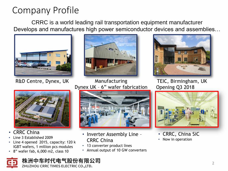
Company Profile
R&D Centre, Dynex, UK Manufacturing
Dynex UK – 6” wafer fabrication
• CRRC, China SiC• Now in operation
• Inverter Assembly Line –
CRRC China• 13 converter product lines
• Annual output of 10 GW converters
• CRRC China• Line 3 Established 2009
• Line 4 opened 2015, capacity: 120 k
IGBT wafers, 1 million pcs modules
• 8” wafer fab, 6,000 m2, class 10
TEIC, Birmingham, UK
Opening Q3 2018
CRRC is a world leading rail transportation equipment manufacturer
Develops and manufactures high power semiconductor devices and assemblies…
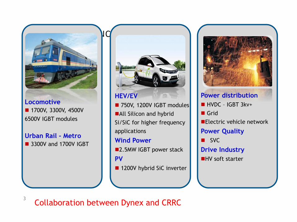
R&D and product Applications
3
Locomotive
1700V, 3300V, 4500V
6500V IGBT modules
Urban Rail - Metro
3300V and 1700V IGBT
HEV/EV
750V, 1200V IGBT modules
All Silicon and hybrid
Si/SiC for higher frequency
applications
Wind Power
2.5MW IGBT power stack
PV
1200V hybrid SiC inverter
Power distribution
HVDC – IGBT 3kv+
Grid
Electric vehicle network
Power Quality
SVC
Drive Industry
HV soft starter
Collaboration between Dynex and CRRC
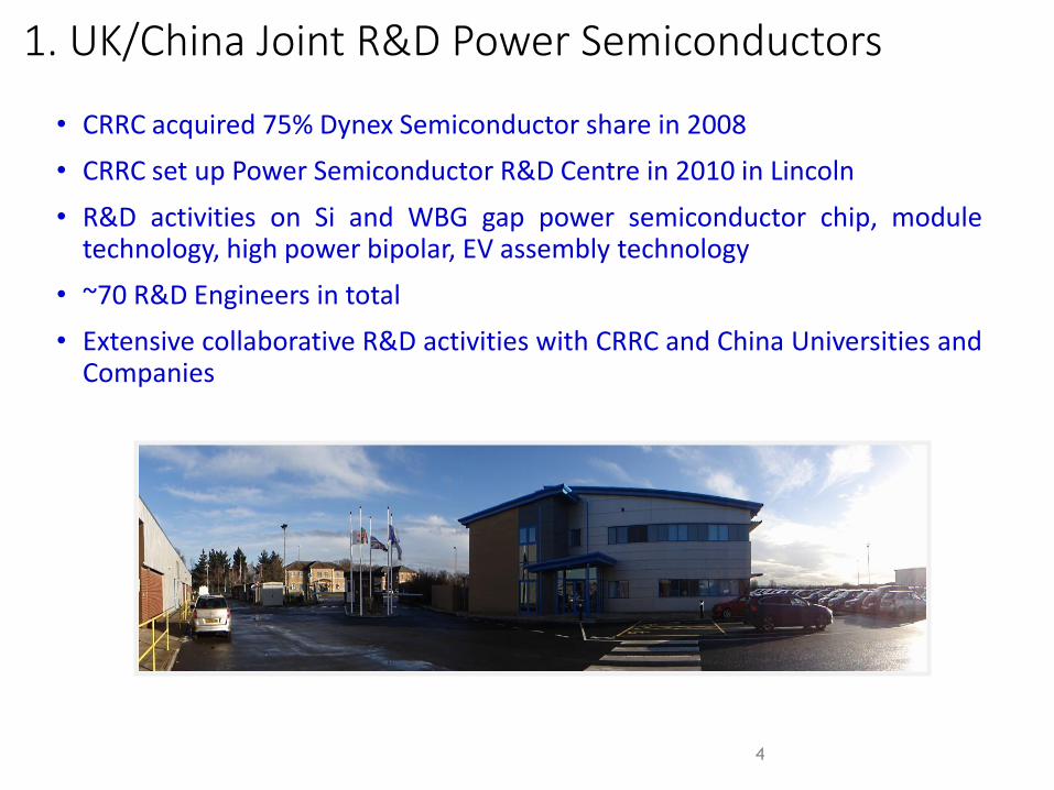
1. UK/China Joint R&D Power Semiconductors
• CRRC acquired 75% Dynex Semiconductor share in 2008
• CRRC set up Power Semiconductor R&D Centre in 2010 in Lincoln
• R&D activities on Si and WBG gap power semiconductor chip, moduletechnology, high power bipolar, EV assembly technology
• ~70 R&D Engineers in total
• Extensive collaborative R&D activities with CRRC and China Universities andCompanies
4
1. UK/China Joint R&D Power Semiconductors
• CRRC funded University of Nottingham projects on IGBT reliability andhealth monitoring for locomotive application
• RD centre works with Nottingham on power module technology, failureanalysis, power cycling test and results analysis
• RD centre collaborating with Nottingham on government, EU and ECPEfounding projects from 2010, the topics were advanced power modulepackaging technology, HEV power train system, integrated cooling,reliability etc.
• CRRC is supporting Nottingham on EPSRC doctoral centre program
• CRRC and Nottingham are looking for wide collaboration in powerelectronics, motor control, reliability etc: CRRC show case in Notting on 11th
Jun
5
1. UK/China Joint R&D Power Semiconductors
• CRRC working with University of Cambridge on IGBT and FRD diedevelopment since 2014
• CRRC has the state-of-the-art 8” chip manufacture line for full voltage (600-6500V) IGBT and FRD wafer processing
• Collaboration is on advanced IGBT and FRD design, simulation andmanufacture
• 4th generation trench field stop IGBT was developed
• Smart IGBT and RC-IGBT are being developed
6
1. UK/China Joint R&D Power Semiconductors
• Through Innovate UK-China bridge collaborative project, University ofCambridge is working with CRRC, Hunan University and Dynex on RC-IGBTdevelopment
• RC-IGBT is an advanced power semiconductor device with great advantagesover conventional trench field stop IGBT
• CRRC has a 6” SiC wafer line and is looking for collaborations with UKUniversities and companies.
• University of Cambridge and CRRC started discussing on SiC devicecollaboration and projects.
7
1. UK/China Joint R&D Power Semiconductors
• Through Innovate UK collaborative project, University of Warwick, Cambridge are working with CRRC on SiC device development
• CRRC collaborated with Warwick on SiC devices design and manufacture,Warwick trained CRRC engineers on SiC devices processing
• University of Warwick working with Chinese Universities and companies onSiC device development and applications
• CRRC supports Warwick on EPSRC doctoral centre program
8
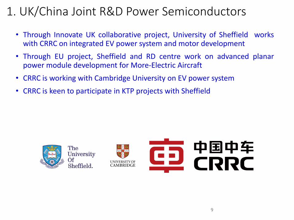
1. UK/China Joint R&D Power Semiconductors
• Through Innovate UK collaborative project, University of Sheffield workswith CRRC on integrated EV power system and motor development
• Through EU project, Sheffield and RD centre work on advanced planarpower module development for More-Electric Aircraft
• CRRC is working with Cambridge University on EV power system
• CRRC is keen to participate in KTP projects with Sheffield
9
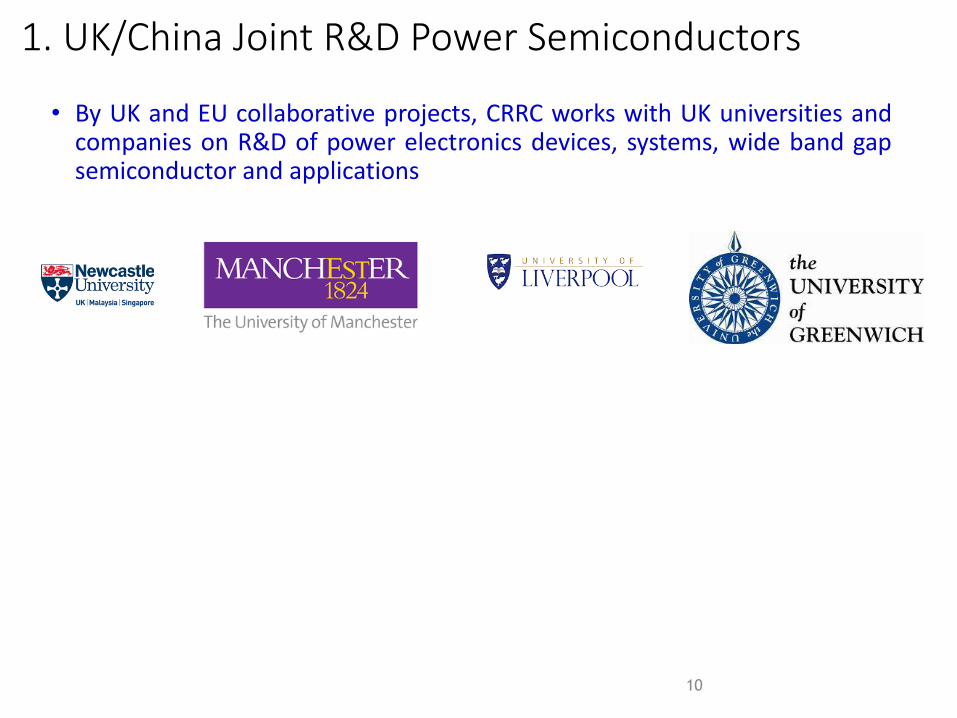
1. UK/China Joint R&D Power Semiconductors
• By UK and EU collaborative projects, CRRC works with UK universities andcompanies on R&D of power electronics devices, systems, wide band gapsemiconductor and applications
10
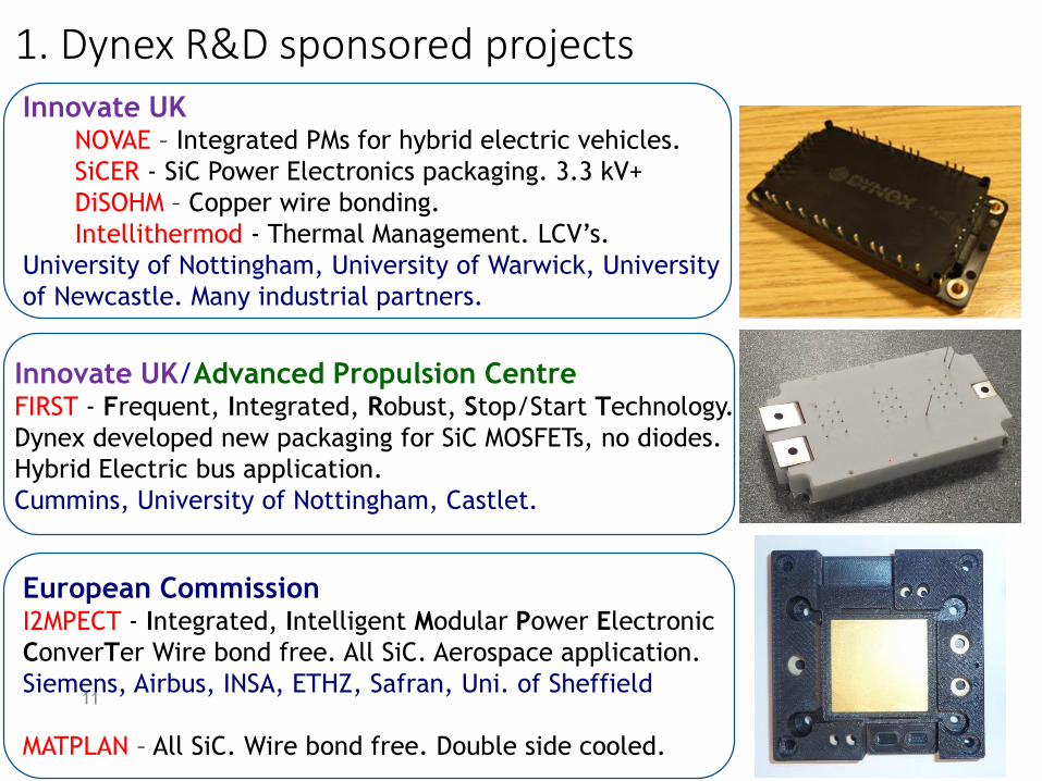
1. Dynex R&D sponsored projects
11
Innovate UK NOVAE – Integrated PMs for hybrid electric vehicles.
SiCER - SiC Power Electronics packaging. 3.3 kV+
DiSOHM – Copper wire bonding.
Intellithermod - Thermal Management. LCV’s.
University of Nottingham, University of Warwick, University
of Newcastle. Many industrial partners.
Innovate UK/Advanced Propulsion CentreFIRST - Frequent, Integrated, Robust, Stop/Start Technology.
Dynex developed new packaging for SiC MOSFETs, no diodes.
Hybrid Electric bus application.
Cummins, University of Nottingham, Castlet.
European CommissionI2MPECT - Integrated, Intelligent Modular Power Electronic
ConverTer Wire bond free. All SiC. Aerospace application.
Siemens, Airbus, INSA, ETHZ, Safran, Uni. of Sheffield
MATPLAN – All SiC. Wire bond free. Double side cooled.
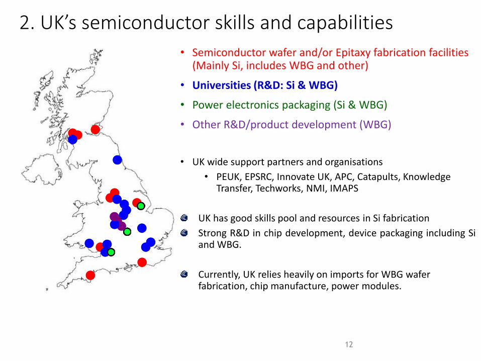
2. UK’s semiconductor skills and capabilities
• Semiconductor wafer and/or Epitaxy fabrication facilities (Mainly Si, includes WBG and other)
• Universities (R&D: Si & WBG)
• Power electronics packaging (Si & WBG)
• Other R&D/product development (WBG)
• UK wide support partners and organisations
• PEUK, EPSRC, Innovate UK, APC, Catapults, Knowledge Transfer, Techworks, NMI, IMAPS
UK has good skills pool and resources in Si fabrication
Strong R&D in chip development, device packaging including Siand WBG.
Currently, UK relies heavily on imports for WBG wafer fabrication, chip manufacture, power modules.
12
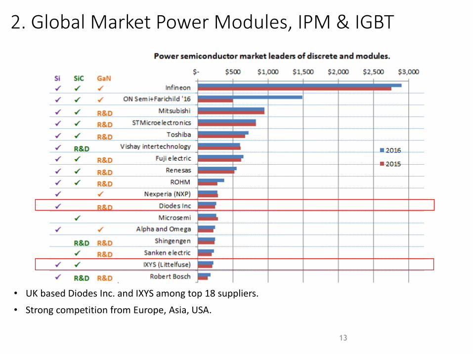
• UK based Diodes Inc. and IXYS among top 18 suppliers.
• Strong competition from Europe, Asia, USA.
13
2. Global Market Power Modules, IPM & IGBT
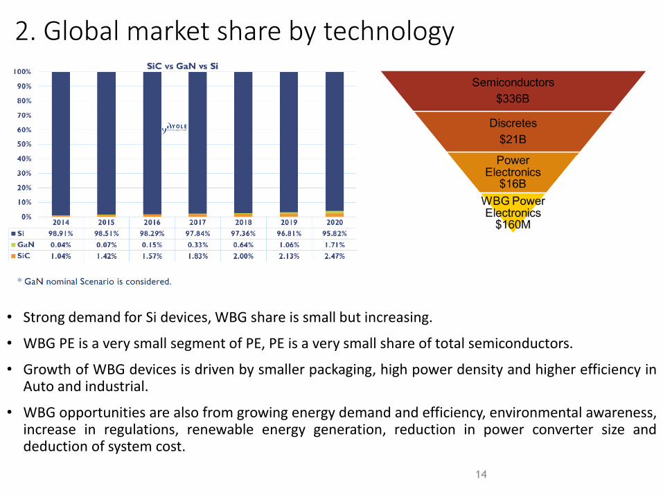
2. Global market share by technology
• Strong demand for Si devices, WBG share is small but increasing.
• WBG PE is a very small segment of PE, PE is a very small share of total semiconductors.
• Growth of WBG devices is driven by smaller packaging, high power density and higher efficiency inAuto and industrial.
• WBG opportunities are also from growing energy demand and efficiency, environmental awareness,increase in regulations, renewable energy generation, reduction in power converter size anddeduction of system cost.
14
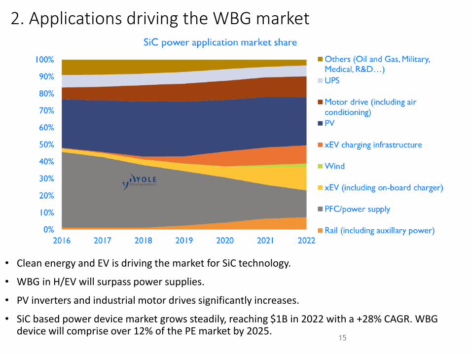
2. Applications driving the WBG market
• Clean energy and EV is driving the market for SiC technology.
• WBG in H/EV will surpass power supplies.
• PV inverters and industrial motor drives significantly increases.
• SiC based power device market grows steadily, reaching $1B in 2022 with a +28% CAGR. WBG device will comprise over 12% of the PE market by 2025.
15
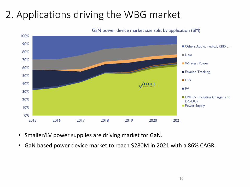
2. Applications driving the WBG market
• Smaller/LV power supplies are driving market for GaN.
• GaN based power device market to reach $280M in 2021 with a 86% CAGR.
16
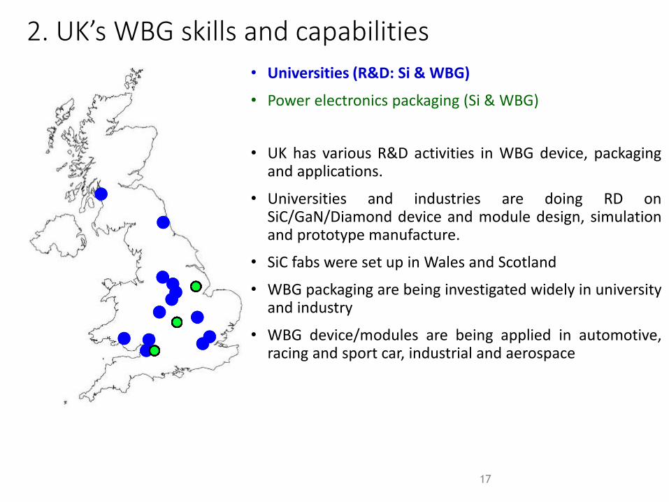
2. UK’s WBG skills and capabilities
17
• Universities (R&D: Si & WBG)
• Power electronics packaging (Si & WBG)
• UK has various R&D activities in WBG device, packagingand applications.
• Universities and industries are doing RD onSiC/GaN/Diamond device and module design, simulationand prototype manufacture.
• SiC fabs were set up in Wales and Scotland
• WBG packaging are being investigated widely in universityand industry
• WBG device/modules are being applied in automotive,racing and sport car, industrial and aerospace
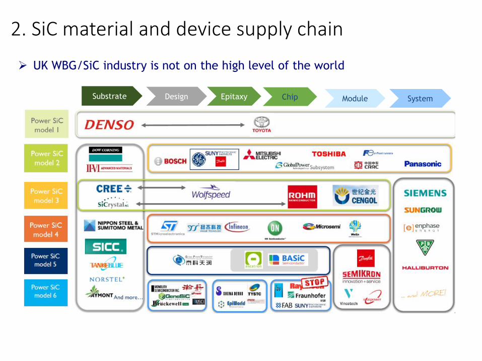
2. SiC material and device supply chain
UK WBG/SiC industry is not on the high level of the world
Substrate Design Epitaxy Chip Module System
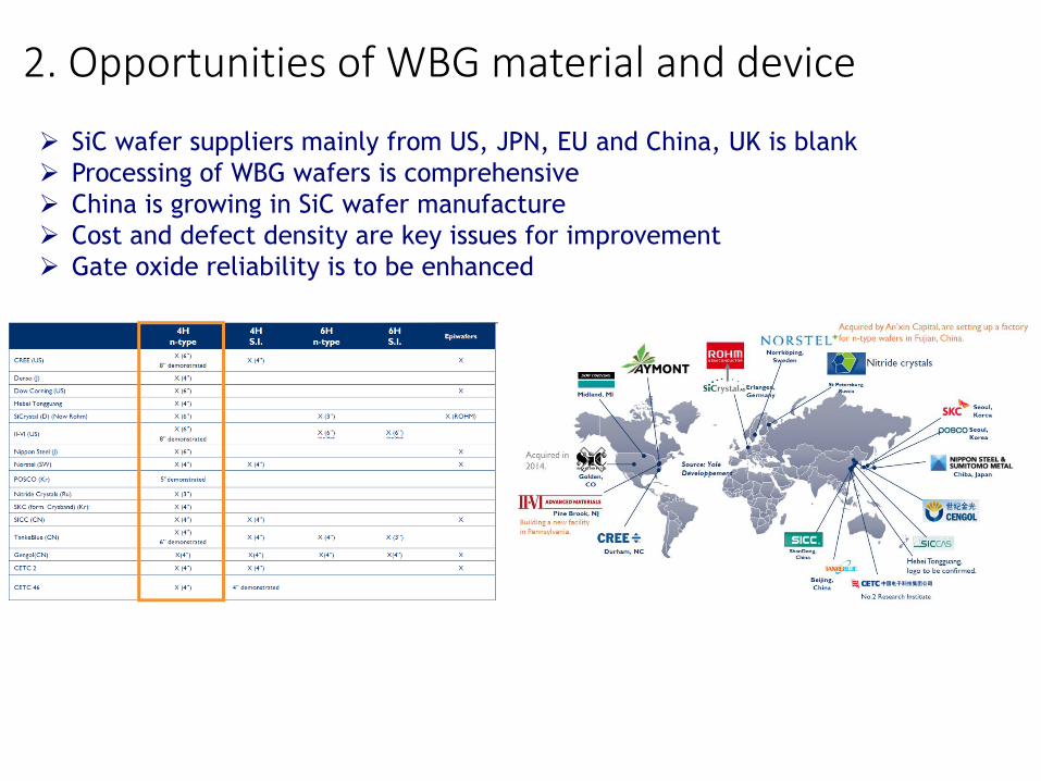
2. Opportunities of WBG material and device
SiC wafer suppliers mainly from US, JPN, EU and China, UK is blank
Processing of WBG wafers is comprehensive
China is growing in SiC wafer manufacture
Cost and defect density are key issues for improvement
Gate oxide reliability is to be enhanced
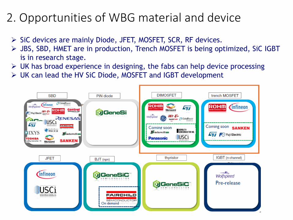
2. Opportunities of WBG material and device
SiC devices are mainly Diode, JFET, MOSFET, SCR, RF devices.
JBS, SBD, HMET are in production, Trench MOSFET is being optimized, SiC IGBT
is in research stage.
UK has broad experience in designing, the fabs can help device processing
UK can lead the HV SiC Diode, MOSFET and IGBT development
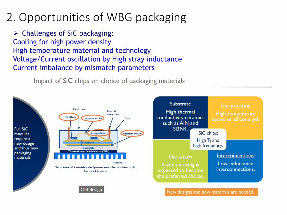
2. Opportunities of WBG packaging Challenges of SiC packaging:
Cooling for high power density
High temperature material and technology
Voltage/Current oscillation by High stray inductance
Current imbalance by mismatch parameters
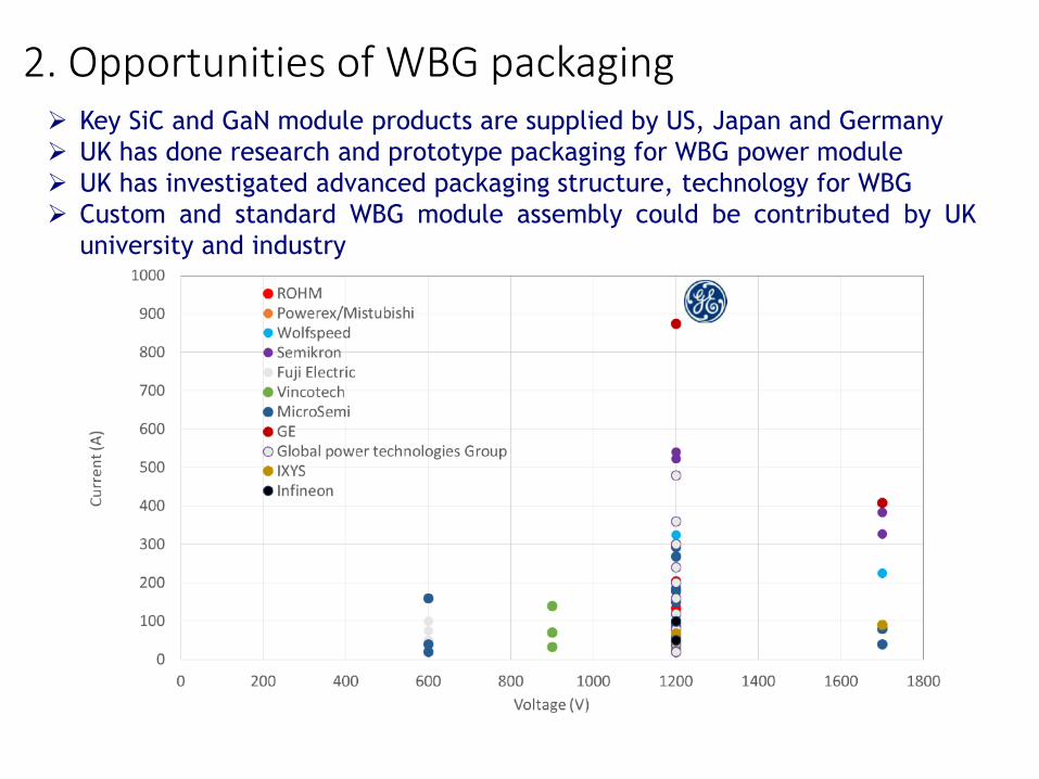
2. Opportunities of WBG packaging Key SiC and GaN module products are supplied by US, Japan and Germany
UK has done research and prototype packaging for WBG power module
UK has investigated advanced packaging structure, technology for WBG
Custom and standard WBG module assembly could be contributed by UK
university and industry
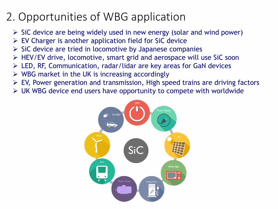
2. Opportunities of WBG application SiC device are being widely used in new energy (solar and wind power)
EV Charger is another application field for SiC device
SiC device are tried in locomotive by Japanese companies
HEV/EV drive, locomotive, smart grid and aerospace will use SiC soon
LED, RF, Communication, radar/lidar are key areas for GaN devices
WBG market in the UK is increasing accordingly
EV, Power generation and transmission, High speed trains are driving factors
UK WBG device end users have opportunity to compete with worldwide
3. Summary CRRC WBG RD activities and collaboration with UK are widely
WBG industrial chains are formed in US, Japan and EU
WBG wafer is limiting device performance and industry development
China is setting up own industrial chain, and start to play roles in all stages
UK has seen opportunities in WBG device design, manufacture and applications