Embed Size (px)
Citation preview
SAND REPORTSAND2011-2515Unlimited ReleasePrinted May 2011
XyceTM Parallel ElectronicSimulator
Users’ Guide, Version 5.2
Eric R. Keiter, Ting Mei, Thomas V. Russo, Eric L. Rankin, Roger P. Pawlowski,Richard L. Schiek, Keith R. Santarelli, Todd S. Coffey, Heidi K. Thornquist,Christina E. Warrender, Deborah A. Fixel
Prepared bySandia National LaboratoriesAlbuquerque, New Mexico 87185 and Livermore, California 94550
Sandia National Laboratories is a multi-program laboratory managed and operated by Sandia Corporation,a wholly owned subsidiary of Lockheed Martin Corporation, for the U.S. Department of EnergysNational Nuclear Security Administration under contract DE-AC04-94AL85000.
Approved for public release; further dissemination unlimited.

Issued by Sandia National Laboratories, operated for the United States Department ofEnergy by Sandia Corporation.
NOTICE: This report was prepared as an account of work sponsored by an agency ofthe United States Government. Neither the United States Government, nor any agencythereof, nor any of their employees, nor any of their contractors, subcontractors, or theiremployees, make any warranty, express or implied, or assume any legal liability or re-sponsibility for the accuracy, completeness, or usefulness of any information, appara-tus, product, or process disclosed, or represent that its use would not infringe privatelyowned rights. Reference herein to any specific commercial product, process, or serviceby trade name, trademark, manufacturer, or otherwise, does not necessarily constituteor imply its endorsement, recommendation, or favoring by the United States Govern-ment, any agency thereof, or any of their contractors or subcontractors. The views andopinions expressed herein do not necessarily state or reflect those of the United StatesGovernment, any agency thereof, or any of their contractors.
Printed in the United States of America. This report has been reproduced directly fromthe best available copy.
Available to DOE and DOE contractors fromU.S. Department of EnergyOffice of Scientific and Technical InformationP.O. Box 62Oak Ridge, TN 37831
Telephone: (865) 576-8401Facsimile: (865) 576-5728E-Mail: [email protected] ordering: http://www.doe.gov/bridge
Available to the public fromU.S. Department of CommerceNational Technical Information Service5285 Port Royal RdSpringfield, VA 22161
Telephone: (800) 553-6847Facsimile: (703) 605-6900E-Mail: [email protected] ordering: http://www.ntis.gov/ordering.htm
DEP
ARTMENT OF ENERGY
• • UN
ITED
STATES OF AM
ERIC
A
2
XyceTM Users’ Guide
SAND2011-2515Unlimited ReleasePrinted May 2011
XyceTM Parallel Electronic Simulator
Users’ Guide, Version 5.2
Eric R. Keiter, Ting Mei, Thomas V. Russo, Eric L. Rankin,Richard L. Schiek, and Heidi K. Thornquist
Electrical Systems Modeling
Deborah A. FixelAdvanced Device Technologies
Todd S. CoffeyComputational Simulation Infrastructure
Roger P. PawlowskiMultiphysics Simulation Technology
Keith R. Santarelli
Christina E. WarrenderCognitive Modeling
Sandia National LaboratoriesP.O. Box 5800Mail Stop 0316
Albuquerque, NM 87185-0316
3

May 13, 2011
Abstract
This manual describes the use of the Xyce Parallel Electronic Simulator. Xyce hasbeen designed as a SPICE-compatible, high-performance analog circuit simulator, andhas been written to support the simulation needs of the Sandia National Laboratorieselectrical designers. This development has focused on improving capability over thecurrent state-of-the-art in the following areas:
Capability to solve extremely large circuit problems by supporting large-scale par-allel computing platforms (up to thousands of processors). Note that this includessupport for most popular parallel and serial computers.
Improved performance for all numerical kernels (e.g., time integrator, nonlinearand linear solvers) through state-of-the-art algorithms and novel techniques.
Device models which are specifically tailored to meet Sandia’s needs, includingsome radiation-aware devices (for Sandia users only).
Object-oriented code design and implementation using modern coding practicesthat ensure that the Xyce Parallel Electronic Simulator will be maintainable andextensible far into the future.
Xyce is a parallel code in the most general sense of the phrase - a message passingparallel implementation - which allows it to run efficiently on the widest possible numberof computing platforms. These include serial, shared-memory and distributed-memoryparallel as well as heterogeneous platforms. Careful attention has been paid to thespecific nature of circuit-simulation problems to ensure that optimal parallel efficiencyis achieved as the number of processors grows.
The development of Xyce provides a platform for computational research and de-velopment aimed specifically at the needs of the Laboratory. With Xyce, Sandia hasan “in-house” capability with which both new electrical (e.g., device model develop-ment) and algorithmic (e.g., faster time-integration methods, parallel solver algorithms)research and development can be performed. As a result, Xyce is a unique electricalsimulation capability, designed to meet the unique needs of the laboratory.
4

XyceTM Users’ Guide
Acknowledgements
The authors would like to acknowledge the entire Sandia National Laboratories HPEMS(High Performance Electrical Modeling and Simulation) team, including Steve Wix, CarolynBogdan, Regina Schells, Ken Marx, Steve Brandon and Bill Ballard, for their support onthis project.
Trademarks
The information herein is subject to change without notice.
Copyright c© 2002-2011 Sandia Corporation. All rights reserved.
XyceTM Electronic Simulator and XyceTM trademarks of Sandia Corporation.
Portions of the XyceTM code are:Copyright c© 2002, The Regents of the University of California.Produced at the Lawrence Livermore National Laboratory.Written by Alan Hindmarsh, Allan Taylor, Radu Serban.UCRL-CODE-2002-59All rights reserved.
Orcad, Orcad Capture, PSpice and Probe are registered trademarks of Cadence DesignSystems, Inc.
Silicon Graphics, the Silicon Graphics logo and IRIX are registered trademarks of SiliconGraphics, Inc.
Microsoft, Windows and Windows 2000 are registered trademark of Microsoft Corporation.
Solaris and UltraSPARC are registered trademarks of Sun Microsystems Corporation.
Medici, DaVinci and Taurus are registered trademarks of Synopsys Corporation.
HP and Alpha are registered trademarks of Hewlett-Packard company.
Amtec and TecPlot are trademarks of Amtec Engineering, Inc.
Xyce’s expression library is based on that inside Spice 3F5 developed by the EECS De-partment at the University of California.
The EKV3 MOSFET model was developed by the EKV Team of the Electronics Laboratory-TUC of the Technical University of Crete.
All other trademarks are property of their respective owners.
5

XyceTM Users’ Guide
Contacts
Bug Reportshttp://joseki.sandia.gov/bugzilla
http://charleston.sandia.gov/bugzilla
World Wide Webhttp://xyce.sandia.gov
http://charleston.sandia.gov/xyce
Email [email protected]
6
Contents
1. Introduction 191.1 Xyce Overview. . . . . . . . . . . . . . . . . . . . . . . . . . . . . . . . . . . . . . . . . . . . . . . . . . . . . . . . . . . . . . . . 201.2 Xyce Capabilities . . . . . . . . . . . . . . . . . . . . . . . . . . . . . . . . . . . . . . . . . . . . . . . . . . . . . . . . . . . . . 20
Support for Large-Scale Parallel Computing . . . . . . . . . . . . . . . . . . . . . . . . . . . 20Improved Performance for all Numerical Kernels . . . . . . . . . . . . . . . . . . . . . . . 20Device Model Support . . . . . . . . . . . . . . . . . . . . . . . . . . . . . . . . . . . . . . . . . . . . . 21
1.3 Reference Guide . . . . . . . . . . . . . . . . . . . . . . . . . . . . . . . . . . . . . . . . . . . . . . . . . . . . . . . . . . . . . . 211.4 How to Use this Guide . . . . . . . . . . . . . . . . . . . . . . . . . . . . . . . . . . . . . . . . . . . . . . . . . . . . . . . . 211.5 Third Party License Information . . . . . . . . . . . . . . . . . . . . . . . . . . . . . . . . . . . . . . . . . . . . . . . 23
2. Installing and Running Xyce 252.1 Xyce Installation . . . . . . . . . . . . . . . . . . . . . . . . . . . . . . . . . . . . . . . . . . . . . . . . . . . . . . . . . . . . . . 26
Installing Xyce on UNIX . . . . . . . . . . . . . . . . . . . . . . . . . . . . . . . . . . . . . . . . . . . 26Installing Xyce on Microsoft Windows . . . . . . . . . . . . . . . . . . . . . . . . . . . . . . . . 26Important Notes . . . . . . . . . . . . . . . . . . . . . . . . . . . . . . . . . . . . . . . . . . . . . . . . . . 27Uninstalling Xyce . . . . . . . . . . . . . . . . . . . . . . . . . . . . . . . . . . . . . . . . . . . . . . . . . 27
2.2 Running Xyce . . . . . . . . . . . . . . . . . . . . . . . . . . . . . . . . . . . . . . . . . . . . . . . . . . . . . . . . . . . . . . . . . 28Command Line Simulation . . . . . . . . . . . . . . . . . . . . . . . . . . . . . . . . . . . . . . . . . 28Command Line Options . . . . . . . . . . . . . . . . . . . . . . . . . . . . . . . . . . . . . . . . . . . . 29Running Xyce in Parallel . . . . . . . . . . . . . . . . . . . . . . . . . . . . . . . . . . . . . . . . . . . 31Accessing the Microsoft Windows Command Line . . . . . . . . . . . . . . . . . . . . . . 31
3. Simulation Examples with Xyce 393.1 Example Circuit Construction . . . . . . . . . . . . . . . . . . . . . . . . . . . . . . . . . . . . . . . . . . . . . . . . . . 403.2 DC Sweep Analysis . . . . . . . . . . . . . . . . . . . . . . . . . . . . . . . . . . . . . . . . . . . . . . . . . . . . . . . . . . . 423.3 Transient Analysis . . . . . . . . . . . . . . . . . . . . . . . . . . . . . . . . . . . . . . . . . . . . . . . . . . . . . . . . . . . . . 45
4. Netlist Basics 494.1 General Overview . . . . . . . . . . . . . . . . . . . . . . . . . . . . . . . . . . . . . . . . . . . . . . . . . . . . . . . . . . . . . 50
Introduction . . . . . . . . . . . . . . . . . . . . . . . . . . . . . . . . . . . . . . . . . . . . . . . . . . . . . 50
7
XyceTM Users’ Guide CONTENTS
Nodes . . . . . . . . . . . . . . . . . . . . . . . . . . . . . . . . . . . . . . . . . . . . . . . . . . . . . . . . . . 50Elements . . . . . . . . . . . . . . . . . . . . . . . . . . . . . . . . . . . . . . . . . . . . . . . . . . . . . . . 51
4.2 Devices Available for Simulation . . . . . . . . . . . . . . . . . . . . . . . . . . . . . . . . . . . . . . . . . . . . . . . 54Analog Devices . . . . . . . . . . . . . . . . . . . . . . . . . . . . . . . . . . . . . . . . . . . . . . . . . . 54
4.3 Parameters and Expressions . . . . . . . . . . . . . . . . . . . . . . . . . . . . . . . . . . . . . . . . . . . . . . . . . . 56Parameters . . . . . . . . . . . . . . . . . . . . . . . . . . . . . . . . . . . . . . . . . . . . . . . . . . . . . . 56How to Declare and Use Parameters . . . . . . . . . . . . . . . . . . . . . . . . . . . . . . . . . 56Global Parameters . . . . . . . . . . . . . . . . . . . . . . . . . . . . . . . . . . . . . . . . . . . . . . . . 58Expressions . . . . . . . . . . . . . . . . . . . . . . . . . . . . . . . . . . . . . . . . . . . . . . . . . . . . . 59
5. Working with .MODEL Statements and Subcircuit Models 675.1 Definition of a Model . . . . . . . . . . . . . . . . . . . . . . . . . . . . . . . . . . . . . . . . . . . . . . . . . . . . . . . . . . 68
Defining models using model parameters . . . . . . . . . . . . . . . . . . . . . . . . . . . . . 68Defining models using subcircuit netlists . . . . . . . . . . . . . . . . . . . . . . . . . . . . . . 69
5.2 Model Organization . . . . . . . . . . . . . . . . . . . . . . . . . . . . . . . . . . . . . . . . . . . . . . . . . . . . . . . . . . . 72Model libraries . . . . . . . . . . . . . . . . . . . . . . . . . . . . . . . . . . . . . . . . . . . . . . . . . . . 72Model library configuration . . . . . . . . . . . . . . . . . . . . . . . . . . . . . . . . . . . . . . . . . 72
5.3 Model Interpolation. . . . . . . . . . . . . . . . . . . . . . . . . . . . . . . . . . . . . . . . . . . . . . . . . . . . . . . . . . . . 74
6. Analog Behavioral Modeling 776.1 Overview of Analog Behavioral Modeling . . . . . . . . . . . . . . . . . . . . . . . . . . . . . . . . . . . . . . 786.2 Specifying ABM Devices . . . . . . . . . . . . . . . . . . . . . . . . . . . . . . . . . . . . . . . . . . . . . . . . . . . . . . 78
Additional constructs for use in ABM expressions . . . . . . . . . . . . . . . . . . . . . . . 79Examples of Analog Behavioral Modeling . . . . . . . . . . . . . . . . . . . . . . . . . . . . . 80Alternate behavioral modeling sources . . . . . . . . . . . . . . . . . . . . . . . . . . . . . . . 81
6.3 Guidance for ABM Use . . . . . . . . . . . . . . . . . . . . . . . . . . . . . . . . . . . . . . . . . . . . . . . . . . . . . . . . 81ABM devices add equations to the system of equations used by the solver . . 81All expressions used in ABM devices must be valid for any possible input . . . 82ABM devices should not be used purely for output post-processing . . . . . . . . 83
7. Analysis Types 857.1 Introduction . . . . . . . . . . . . . . . . . . . . . . . . . . . . . . . . . . . . . . . . . . . . . . . . . . . . . . . . . . . . . . . . . . . 867.2 Steady-State (.DC) Analysis . . . . . . . . . . . . . . . . . . . . . . . . . . . . . . . . . . . . . . . . . . . . . . . . . . . 86
.DC Statement . . . . . . . . . . . . . . . . . . . . . . . . . . . . . . . . . . . . . . . . . . . . . . . . . . . 86Setting Up and Running a DC Sweep . . . . . . . . . . . . . . . . . . . . . . . . . . . . . . . . 87OP Analysis . . . . . . . . . . . . . . . . . . . . . . . . . . . . . . . . . . . . . . . . . . . . . . . . . . . . . 87
7.3 Transient Analysis . . . . . . . . . . . . . . . . . . . . . . . . . . . . . . . . . . . . . . . . . . . . . . . . . . . . . . . . . . . . . 87.TRAN Statement . . . . . . . . . . . . . . . . . . . . . . . . . . . . . . . . . . . . . . . . . . . . . . . . . 89Defining a Time-Dependent (transient) Source . . . . . . . . . . . . . . . . . . . . . . . . . 90Transient Calculation Time Steps . . . . . . . . . . . . . . . . . . . . . . . . . . . . . . . . . . . . 91Transient Time Step Selection Advice . . . . . . . . . . . . . . . . . . . . . . . . . . . . . . . . 91
8

CONTENTS XyceTM Users’ Guide
Checkpointing and Restarting . . . . . . . . . . . . . . . . . . . . . . . . . . . . . . . . . . . . . . . 937.4 STEP Parametric Analysis . . . . . . . . . . . . . . . . . . . . . . . . . . . . . . . . . . . . . . . . . . . . . . . . . . . . 95
.STEP Statement . . . . . . . . . . . . . . . . . . . . . . . . . . . . . . . . . . . . . . . . . . . . . . . . . 95Sweeping over a Device Instance Parameter . . . . . . . . . . . . . . . . . . . . . . . . . . 95Sweeping over a Device Model Parameter . . . . . . . . . . . . . . . . . . . . . . . . . . . . 96Sweeping over Temperature . . . . . . . . . . . . . . . . . . . . . . . . . . . . . . . . . . . . . . . . 96Special cases: Sweeping Independent Sources, Resistors, Capacitors . . . . . 96Output files . . . . . . . . . . . . . . . . . . . . . . . . . . . . . . . . . . . . . . . . . . . . . . . . . . . . . . 99
7.5 Harmonic Balance Analysis . . . . . . . . . . . . . . . . . . . . . . . . . . . . . . . . . . . . . . . . . . . . . . . . . . . 101.HB Statement . . . . . . . . . . . . . . . . . . . . . . . . . . . . . . . . . . . . . . . . . . . . . . . . . . . 101HB Options . . . . . . . . . . . . . . . . . . . . . . . . . . . . . . . . . . . . . . . . . . . . . . . . . . . . . . 101HB Related Options . . . . . . . . . . . . . . . . . . . . . . . . . . . . . . . . . . . . . . . . . . . . . . . 102
7.6 Multi-Time PDE (MPDE) Analysis . . . . . . . . . . . . . . . . . . . . . . . . . . . . . . . . . . . . . . . . . . . . . 103MPDE Usage . . . . . . . . . . . . . . . . . . . . . . . . . . . . . . . . . . . . . . . . . . . . . . . . . . . . 103Driven Circuit Example: Gilbert Cell . . . . . . . . . . . . . . . . . . . . . . . . . . . . . . . . . . 105
8. Using Homotopy Algorithms to Obtain Operating Points 1098.1 Homotopy Algorithms Overview . . . . . . . . . . . . . . . . . . . . . . . . . . . . . . . . . . . . . . . . . . . . . . . 110
HOMOTOPY Algorithms Available in Xyce . . . . . . . . . . . . . . . . . . . . . . . . . . . . 1108.2 MOSFET Homotopy. . . . . . . . . . . . . . . . . . . . . . . . . . . . . . . . . . . . . . . . . . . . . . . . . . . . . . . . . . .111
Explanation of Parameters, Best Practice . . . . . . . . . . . . . . . . . . . . . . . . . . . . . 1128.3 Natural Parameter Homotopy . . . . . . . . . . . . . . . . . . . . . . . . . . . . . . . . . . . . . . . . . . . . . . . . . .112
Explanation of Parameters, Best Practice . . . . . . . . . . . . . . . . . . . . . . . . . . . . . 1148.4 Natural Multi-Parameter Homotopy . . . . . . . . . . . . . . . . . . . . . . . . . . . . . . . . . . . . . . . . . . . .114
Explanation of Parameters, Best Practice . . . . . . . . . . . . . . . . . . . . . . . . . . . . . 1148.5 GMIN Stepping . . . . . . . . . . . . . . . . . . . . . . . . . . . . . . . . . . . . . . . . . . . . . . . . . . . . . . . . . . . . . . . 116
Explanation of Parameters, Best Practice . . . . . . . . . . . . . . . . . . . . . . . . . . . . . 1168.6 Pseudo Transient. . . . . . . . . . . . . . . . . . . . . . . . . . . . . . . . . . . . . . . . . . . . . . . . . . . . . . . . . . . . . .116
Explanation of Parameters, Best Practice . . . . . . . . . . . . . . . . . . . . . . . . . . . . . 119
9. Results Output and Evaluation Options 1219.1 Control of Results Output. . . . . . . . . . . . . . . . . . . . . . . . . . . . . . . . . . . . . . . . . . . . . . . . . . . . . .122
.PRINT Command . . . . . . . . . . . . . . . . . . . . . . . . . . . . . . . . . . . . . . . . . . . . . . . . 1229.2 Additional Output Options . . . . . . . . . . . . . . . . . . . . . . . . . . . . . . . . . . . . . . . . . . . . . . . . . . . . .122
.OPTIONS OUTPUT Command . . . . . . . . . . . . . . . . . . . . . . . . . . . . . . . . . . . . . . . 1229.3 Graphical Display of Solution Results . . . . . . . . . . . . . . . . . . . . . . . . . . . . . . . . . . . . . . . . . .124
10.Guidance for Running Xyce in Parallel 12710.1 Introduction . . . . . . . . . . . . . . . . . . . . . . . . . . . . . . . . . . . . . . . . . . . . . . . . . . . . . . . . . . . . . . . . . . .12810.2 Mechanics . . . . . . . . . . . . . . . . . . . . . . . . . . . . . . . . . . . . . . . . . . . . . . . . . . . . . . . . . . . . . . . . . . . .12810.3 Problem Size. . . . . . . . . . . . . . . . . . . . . . . . . . . . . . . . . . . . . . . . . . . . . . . . . . . . . . . . . . . . . . . . . .128
9

XyceTM Users’ Guide CONTENTS
Smallest Possible Problem Size . . . . . . . . . . . . . . . . . . . . . . . . . . . . . . . . . . . . . 128Ideal Problem Size . . . . . . . . . . . . . . . . . . . . . . . . . . . . . . . . . . . . . . . . . . . . . . . . 129
10.4 Linear Solver Options . . . . . . . . . . . . . . . . . . . . . . . . . . . . . . . . . . . . . . . . . . . . . . . . . . . . . . . . .129AztecOO . . . . . . . . . . . . . . . . . . . . . . . . . . . . . . . . . . . . . . . . . . . . . . . . . . . . . . . . 130KLU . . . . . . . . . . . . . . . . . . . . . . . . . . . . . . . . . . . . . . . . . . . . . . . . . . . . . . . . . . . . 132SuperLU . . . . . . . . . . . . . . . . . . . . . . . . . . . . . . . . . . . . . . . . . . . . . . . . . . . . . . . . 133
10.5 Transformation Options. . . . . . . . . . . . . . . . . . . . . . . . . . . . . . . . . . . . . . . . . . . . . . . . . . . . . . . .133Partitioning the Linear System . . . . . . . . . . . . . . . . . . . . . . . . . . . . . . . . . . . . . . 133Singleton Filtering of the Linear System . . . . . . . . . . . . . . . . . . . . . . . . . . . . . . 135AMD Ordering of the Linear System . . . . . . . . . . . . . . . . . . . . . . . . . . . . . . . . . 135Permuting the Linear System to Block Triangular Form . . . . . . . . . . . . . . . . . . 135
11.Handling Power Node Parasitics 13711.1 Power Node Parasitics . . . . . . . . . . . . . . . . . . . . . . . . . . . . . . . . . . . . . . . . . . . . . . . . . . . . . . . . 13811.2 Two Level Algorithms Overview. . . . . . . . . . . . . . . . . . . . . . . . . . . . . . . . . . . . . . . . . . . . . . . .13911.3 Examples . . . . . . . . . . . . . . . . . . . . . . . . . . . . . . . . . . . . . . . . . . . . . . . . . . . . . . . . . . . . . . . . . . . . .139
Explanation and Guidance . . . . . . . . . . . . . . . . . . . . . . . . . . . . . . . . . . . . . . . . . 13911.4 Restart . . . . . . . . . . . . . . . . . . . . . . . . . . . . . . . . . . . . . . . . . . . . . . . . . . . . . . . . . . . . . . . . . . . . . . . .142
12.Specifying Initial Conditions 14312.1 Initial Conditions Overview . . . . . . . . . . . . . . . . . . . . . . . . . . . . . . . . . . . . . . . . . . . . . . . . . . . . 14412.2 Device Level IC= Specification . . . . . . . . . . . . . . . . . . . . . . . . . . . . . . . . . . . . . . . . . . . . . . . . 14512.3 .IC and .DCVOLT Initial Condition Statements . . . . . . . . . . . . . . . . . . . . . . . . . . . . . . . . . 147
Syntax . . . . . . . . . . . . . . . . . . . . . . . . . . . . . . . . . . . . . . . . . . . . . . . . . . . . . . . . . . 147Example . . . . . . . . . . . . . . . . . . . . . . . . . . . . . . . . . . . . . . . . . . . . . . . . . . . . . . . . 148
12.4 .NODESET Initial Condition Statements . . . . . . . . . . . . . . . . . . . . . . . . . . . . . . . . . . . . . . .149Example . . . . . . . . . . . . . . . . . . . . . . . . . . . . . . . . . . . . . . . . . . . . . . . . . . . . . . . . 149
12.5 .SAVE Statements . . . . . . . . . . . . . . . . . . . . . . . . . . . . . . . . . . . . . . . . . . . . . . . . . . . . . . . . . . . . 15012.6 DCOP Restart . . . . . . . . . . . . . . . . . . . . . . . . . . . . . . . . . . . . . . . . . . . . . . . . . . . . . . . . . . . . . . . . 151
Saving a DCOP restart file . . . . . . . . . . . . . . . . . . . . . . . . . . . . . . . . . . . . . . . . . 151Loading a DCOP restart file . . . . . . . . . . . . . . . . . . . . . . . . . . . . . . . . . . . . . . . . 151
12.7 UIC and NOOP . . . . . . . . . . . . . . . . . . . . . . . . . . . . . . . . . . . . . . . . . . . . . . . . . . . . . . . . . . . . . . . 153Example . . . . . . . . . . . . . . . . . . . . . . . . . . . . . . . . . . . . . . . . . . . . . . . . . . . . . . . . 153
13.Working with .PREPROCESS Commands 15513.1 Introduction . . . . . . . . . . . . . . . . . . . . . . . . . . . . . . . . . . . . . . . . . . . . . . . . . . . . . . . . . . . . . . . . . . .15613.2 Ground Synonym Replacement . . . . . . . . . . . . . . . . . . . . . . . . . . . . . . . . . . . . . . . . . . . . . . . 15613.3 Removal of Unused Components . . . . . . . . . . . . . . . . . . . . . . . . . . . . . . . . . . . . . . . . . . . . . .15913.4 Adding Resistors to Dangling Nodes. . . . . . . . . . . . . . . . . . . . . . . . . . . . . . . . . . . . . . . . . . .162
14.TCAD (PDE Device) Simulation with Xyce 169
10

CONTENTS XyceTM Users’ Guide
14.1 Introduction . . . . . . . . . . . . . . . . . . . . . . . . . . . . . . . . . . . . . . . . . . . . . . . . . . . . . . . . . . . . . . . . . . .170Equations . . . . . . . . . . . . . . . . . . . . . . . . . . . . . . . . . . . . . . . . . . . . . . . . . . . . . . . 170Discretization . . . . . . . . . . . . . . . . . . . . . . . . . . . . . . . . . . . . . . . . . . . . . . . . . . . . 172
14.2 One Dimensional Example . . . . . . . . . . . . . . . . . . . . . . . . . . . . . . . . . . . . . . . . . . . . . . . . . . . .173Netlist Explanation . . . . . . . . . . . . . . . . . . . . . . . . . . . . . . . . . . . . . . . . . . . . . . . . 173Boundary Conditions and Doping Profile . . . . . . . . . . . . . . . . . . . . . . . . . . . . . . 175Results . . . . . . . . . . . . . . . . . . . . . . . . . . . . . . . . . . . . . . . . . . . . . . . . . . . . . . . . . 176
14.3 Two Dimensional Example . . . . . . . . . . . . . . . . . . . . . . . . . . . . . . . . . . . . . . . . . . . . . . . . . . . . 178Netlist Explanation . . . . . . . . . . . . . . . . . . . . . . . . . . . . . . . . . . . . . . . . . . . . . . . . 178Doping Profile . . . . . . . . . . . . . . . . . . . . . . . . . . . . . . . . . . . . . . . . . . . . . . . . . . . 180Boundary Conditions and Electrode Configuration . . . . . . . . . . . . . . . . . . . . . . 180Results . . . . . . . . . . . . . . . . . . . . . . . . . . . . . . . . . . . . . . . . . . . . . . . . . . . . . . . . . 180
14.4 Doping Profile . . . . . . . . . . . . . . . . . . . . . . . . . . . . . . . . . . . . . . . . . . . . . . . . . . . . . . . . . . . . . . . . .185Manually Specifying the Doping . . . . . . . . . . . . . . . . . . . . . . . . . . . . . . . . . . . . . 185Default Doping Profiles . . . . . . . . . . . . . . . . . . . . . . . . . . . . . . . . . . . . . . . . . . . . 188
14.5 Electrodes . . . . . . . . . . . . . . . . . . . . . . . . . . . . . . . . . . . . . . . . . . . . . . . . . . . . . . . . . . . . . . . . . . . . 190Manually Specifying the Electrodes . . . . . . . . . . . . . . . . . . . . . . . . . . . . . . . . . . 190Electrode Defaults . . . . . . . . . . . . . . . . . . . . . . . . . . . . . . . . . . . . . . . . . . . . . . . . 193
14.6 Meshes . . . . . . . . . . . . . . . . . . . . . . . . . . . . . . . . . . . . . . . . . . . . . . . . . . . . . . . . . . . . . . . . . . . . . . .195Meshes from the SG Framework (External, 2D) . . . . . . . . . . . . . . . . . . . . . . . . 195Cartesian Meshes (Internal, 1D and 2D) . . . . . . . . . . . . . . . . . . . . . . . . . . . . . . 195Cylindrical meshes, 2D . . . . . . . . . . . . . . . . . . . . . . . . . . . . . . . . . . . . . . . . . . . . 196
14.7 Mobility Models . . . . . . . . . . . . . . . . . . . . . . . . . . . . . . . . . . . . . . . . . . . . . . . . . . . . . . . . . . . . . . . 19714.8 Bulk Materials . . . . . . . . . . . . . . . . . . . . . . . . . . . . . . . . . . . . . . . . . . . . . . . . . . . . . . . . . . . . . . . . .19814.9 Solver Options . . . . . . . . . . . . . . . . . . . . . . . . . . . . . . . . . . . . . . . . . . . . . . . . . . . . . . . . . . . . . . . .19914.10Output and Visualization . . . . . . . . . . . . . . . . . . . . . . . . . . . . . . . . . . . . . . . . . . . . . . . . . . . . . . 200
Using the .PRINT Command . . . . . . . . . . . . . . . . . . . . . . . . . . . . . . . . . . . . . . . 200Multi-dimensional Plots . . . . . . . . . . . . . . . . . . . . . . . . . . . . . . . . . . . . . . . . . . . . 200Volume Averaged Data . . . . . . . . . . . . . . . . . . . . . . . . . . . . . . . . . . . . . . . . . . . . 201
11

XyceTM Users’ Guide
12
Figures
2.1 Using the Start Menu . . . . . . . . . . . . . . . . . . . . . . . . . . . . . . . . . . . . . . . . . . . . . . 322.2 Using the Run Dialog Box . . . . . . . . . . . . . . . . . . . . . . . . . . . . . . . . . . . . . . . . . . 322.3 Default Command Line Window . . . . . . . . . . . . . . . . . . . . . . . . . . . . . . . . . . . . . 332.4 Command Line Window: Using runxyce . . . . . . . . . . . . . . . . . . . . . . . . . . . . . . 342.5 Command Line Window: Default runxyce Output . . . . . . . . . . . . . . . . . . . . . . 352.6 Command Line Window: Starting a Simulation . . . . . . . . . . . . . . . . . . . . . . . . . 362.7 Command Line Window: On-screen Output . . . . . . . . . . . . . . . . . . . . . . . . . . . 37
3.1 Diode clipper circuit netlist. . . . . . . . . . . . . . . . . . . . . . . . . . . . . . . . . . . . . . . . . . 413.2 Schematic of diode clipper circuit with DC and transient voltage sources. . . . 423.4 DC sweep voltages at Vin, node 2 and Vout. . . . . . . . . . . . . . . . . . . . . . . . . . . . 433.3 Diode clipper circuit netlist for DC sweep analysis. . . . . . . . . . . . . . . . . . . . . . 443.5 Diode clipper circuit netlist for transient analysis. . . . . . . . . . . . . . . . . . . . . . . . 463.6 Sinusoidal input signal and clipped outputs. . . . . . . . . . . . . . . . . . . . . . . . . . . . 47
5.1 Example subcircuit model. . . . . . . . . . . . . . . . . . . . . . . . . . . . . . . . . . . . . . . . . . 695.2 Example subcircuit model. . . . . . . . . . . . . . . . . . . . . . . . . . . . . . . . . . . . . . . . . . 71
7.1 Diode clipper circuit netlist for DC sweep analysis. . . . . . . . . . . . . . . . . . . . . . . 887.2 DC sweep voltages at Vin, node 2 and Vout. . . . . . . . . . . . . . . . . . . . . . . . . . . . 897.3 Diode clipper circuit netlist for step transient analysis. . . . . . . . . . . . . . . . . . . . 977.4 Diode clipper circuit netlist for 2-step transient analysis. . . . . . . . . . . . . . . . . . 987.5 Gilbert Cell Result . . . . . . . . . . . . . . . . . . . . . . . . . . . . . . . . . . . . . . . . . . . . . . . . 1057.6 Gilbert Cell Result . . . . . . . . . . . . . . . . . . . . . . . . . . . . . . . . . . . . . . . . . . . . . . . . 1067.7 Gilbert Cell MPDE netlist. . . . . . . . . . . . . . . . . . . . . . . . . . . . . . . . . . . . . . . . . . . 107
8.1 Example MOSFET homotopy netlist. . . . . . . . . . . . . . . . . . . . . . . . . . . . . . . . . . 1118.2 Example natural parameter homotopy netlist. . . . . . . . . . . . . . . . . . . . . . . . . . . 1138.3 Example multi-parameter homotopy netlist. This netlist reproduces MOS-
FET homotopy with a manual specification. . . . . . . . . . . . . . . . . . . . . . . . . . . . 115
13
XyceTM Users’ Guide FIGURES
8.4 Example GMIN stepping netlist. Note that the continuation type is 1, and thecontinuation parameter is called GSTEPPING. . . . . . . . . . . . . . . . . . . . . . . . . 117
8.5 Example of Pseudo transient solver options. Note that the continuation pa-rameter is set to 9. . . . . . . . . . . . . . . . . . . . . . . . . . . . . . . . . . . . . . . . . . . . . . . . . 118
9.1 TecPlot plot of diode clipper circuit transient response from Xyce .prn file. . . 125
11.1 Example two-level top netlist. . . . . . . . . . . . . . . . . . . . . . . . . . . . . . . . . . . . . . . . 14011.2 Example two-level inner netlist. . . . . . . . . . . . . . . . . . . . . . . . . . . . . . . . . . . . . . 141
12.1 Example result with and without IC= preset. . . . . . . . . . . . . . . . . . . . . . . . . . . . 14412.2 Example netlist with device-level IC=. . . . . . . . . . . . . . . . . . . . . . . . . . . . . . . . . 14612.3 Example netlist with .IC. Without the .IC statement, the capacitor is not
given an initial charge, and the signals in transient are all flat. With the .ICstatement, it has an initial change which then decays in transient. . . . . . . . . 147
12.4 Example netlist with UIC. This circuit is a pierce oscillator, and it will onlyoscillate if the operating point is skipped. This oscillator will take a reallylong time to achieve its steady-state amplitude if the .IC statement is notincluded. By including the .IC statement, the amplitude of node 2 is presetto a value close to its final steady-state amplitude. Note, the transient in thisexample only goes for 10 cycles as a demonstration. In general, the timescales for this oscillator are much longer than that and require millions ofcycles. . . . . . . . . . . . . . . . . . . . . . . . . . . . . . . . . . . . . . . . . . . . . . . . . . . . . . . . . . 153
13.1 Example netlist where Gnd is treated as being different from node 0. . . . . . . . 15713.2 Circuit diagram corresponding to the netlist of Fig. 13.1 where node Gnd is
treated as being different from node 0. . . . . . . . . . . . . . . . . . . . . . . . . . . . . . . . 15713.3 Example netlist where Gnd is treated as a synonym for node 0. . . . . . . . . . . . . 15813.4 Circuit diagram corresponding to Fig. 13.3 where node Gnd is treated as a
synonym for node 0. . . . . . . . . . . . . . . . . . . . . . . . . . . . . . . . . . . . . . . . . . . . . . . 15813.5 Netlist with a resistor R3 whose device terminals are both the same node
(node 2). . . . . . . . . . . . . . . . . . . . . . . . . . . . . . . . . . . . . . . . . . . . . . . . . . . . . . . . . 15913.6 Circuit of Fig. 13.5 containing a resistor R3 whose terminals are tied to the
same node (node 2). . . . . . . . . . . . . . . . . . . . . . . . . . . . . . . . . . . . . . . . . . . . . . . 16013.7 Circuit with an improperly connected voltage source V2. . . . . . . . . . . . . . . . . . 16013.8 Circuit with an “unused” resistor R3 that gets removed from the netlist. . . . . . 16113.9 Circuit of Fig. 13.8 where the resistor R3 has been removed via the .PREPROCESS
REMOVEUNUSED statement. . . . . . . . . . . . . . . . . . . . . . . . . . . . . . . . . . . . . . . . . . . 16313.10Netlist of circuit with two dangling nodes, nodes 3 and 4. . . . . . . . . . . . . . . . . . 16413.11Schematic of netlist in Fig. 13.10. . . . . . . . . . . . . . . . . . . . . . . . . . . . . . . . . . . . . 165
14
FIGURES XyceTM Users’ Guide
13.12Schematic of a circuit with an incomplete connection between the resistorR2 and node 3. . . . . . . . . . . . . . . . . . . . . . . . . . . . . . . . . . . . . . . . . . . . . . . . . . . . 165
13.13Netlist of circuit with two dangling nodes, nodes 3 and 4, with .PREPROCESSADDRESISTORS statements. . . . . . . . . . . . . . . . . . . . . . . . . . . . . . . . . . . . . . . . . . 166
13.14Output file filename xyce.cir which results from the .PREPROCESS ADDRESISTORstatements for the netlist of Fig. 13.12 (with assumed file name filename). . 167
13.15Schematic corresponding to the Xyce-generated netlist of Fig. 13.14. . . . . . . 168
14.1 MOSFET Mesh Example . . . . . . . . . . . . . . . . . . . . . . . . . . . . . . . . . . . . . . . . . . 17114.2 One dimensional diode netlist. . . . . . . . . . . . . . . . . . . . . . . . . . . . . . . . . . . . . . . 17414.3 Voltage regulator schematic. . . . . . . . . . . . . . . . . . . . . . . . . . . . . . . . . . . . . . . . . 17514.4 Transient Result for voltage regulator . . . . . . . . . . . . . . . . . . . . . . . . . . . . . . . . . 17714.5 Two-dimensional BJT netlist. . . . . . . . . . . . . . . . . . . . . . . . . . . . . . . . . . . . . . . . 17914.6 Two-Dimensional BJT Circuit Schematic . . . . . . . . . . . . . . . . . . . . . . . . . . . . . . 18214.7 Initial Two-Dimensional BJT Result . . . . . . . . . . . . . . . . . . . . . . . . . . . . . . . . . . 18314.8 Final Two-Dimensional BJT Result . . . . . . . . . . . . . . . . . . . . . . . . . . . . . . . . . . . 18314.9 I-V Two-Dimensional BJT Result . . . . . . . . . . . . . . . . . . . . . . . . . . . . . . . . . . . . 18414.10One-dimensional example, with detailed doping. . . . . . . . . . . . . . . . . . . . . . . . 18614.11Doping Profile . . . . . . . . . . . . . . . . . . . . . . . . . . . . . . . . . . . . . . . . . . . . . . . . . . . 18714.12Two-dimensional example, with detailed doping and detailed electrodes. . . . 19114.13Cylindrical Mesh Example. . . . . . . . . . . . . . . . . . . . . . . . . . . . . . . . . . . . . . . . . . 196
15

XyceTM Users’ Guide
16
Tables
1.1 Xyce typographical conventions. . . . . . . . . . . . . . . . . . . . . . . . . . . . . . . . . . . . . 22
2.1 Platform scripts for running Xyce. . . . . . . . . . . . . . . . . . . . . . . . . . . . . . . . . . . . 292.2 List of Xyce command line arguments. . . . . . . . . . . . . . . . . . . . . . . . . . . . . . . . 30
4.1 Analog Device Quick Reference. . . . . . . . . . . . . . . . . . . . . . . . . . . . . . . . . . . . . 564.2 Expression operators . . . . . . . . . . . . . . . . . . . . . . . . . . . . . . . . . . . . . . . . . . . . . . 614.3 Arithmetic Functions in Expressions . . . . . . . . . . . . . . . . . . . . . . . . . . . . . . . . . 624.4 Arithmetic Functions in Expressions (cont’d) . . . . . . . . . . . . . . . . . . . . . . . . . . 634.5 Exponential, Logarithmic, and Trigonometric Functions in Expressions . . . . . 644.6 SPICE Compatibility Functions in Expressions . . . . . . . . . . . . . . . . . . . . . . . . . 65
7.1 Summary of time-dependent sources supported by Xyce. . . . . . . . . . . . . . . . 907.2 Default parameters for independent sources. . . . . . . . . . . . . . . . . . . . . . . . . . . 99
9.1 .PRINT command options. . . . . . . . . . . . . . . . . . . . . . . . . . . . . . . . . . . . . . . . . . 123
10.1 AztecOO linear solver options. . . . . . . . . . . . . . . . . . . . . . . . . . . . . . . . . . . . . . . 13010.2 AztecOO preconditioner options. . . . . . . . . . . . . . . . . . . . . . . . . . . . . . . . . . . . . 13110.3 KLU linear solver options. . . . . . . . . . . . . . . . . . . . . . . . . . . . . . . . . . . . . . . . . . . 13310.4 Partitioning options. . . . . . . . . . . . . . . . . . . . . . . . . . . . . . . . . . . . . . . . . . . . . . . . 134
13.1 List of keywords and device types which can be used in a .PREPROCESSREMOVEUNUSED statement. . . . . . . . . . . . . . . . . . . . . . . . . . . . . . . . . . . . . . . . . . . 162
14.1 Description of the flatx, flaty doping parameters . . . . . . . . . . . . . . . . . . . . . . . . 18814.2 Default Doping profiles for different numbers of electrodes . . . . . . . . . . . . . . . 18914.3 Electrode Material Options . . . . . . . . . . . . . . . . . . . . . . . . . . . . . . . . . . . . . . . . . 19214.4 Mobility models available for PDE devices . . . . . . . . . . . . . . . . . . . . . . . . . . . . . 197
17

XyceTM Users’ Guide
18

1. Introduction
Welcome to XyceThe Xyce Parallel Electronic Simulator is a SPICE-compatible [1] [2] circuit simulator, thathas been written to support the unique simulation needs of electrical designers at SandiaNational Laboratories. It is specifically targeted to run on large-scale parallel computingplatforms but is also available on a variety of architectures including single processor work-stations. It aims to support a variety of devices and models specific to Sandia needs aswell as standard capabilities available from current commercial simulators.
19

XyceTM Users’ Guide Introduction
1.1 Xyce OverviewThe Xyce Parallel Electronic Simulator project was started in 1999 to support the simula-tion needs of electrical designers at Sandia National Laboratories. The current release ofXyce is version 5.2, and the code has evolved into a mature platform for large scale circuitsimulation.
Xyce includes several unique features. In addition to allowing the simulation of circuits ofunprecedented size, Xyce includes novel approaches to numerical kernels including timeintegration algorithms, nonlinear and linear solvers. The primary driver for this numericalinnovation has been the need to simulate very large scale circuits (100,000 devices ormore) on the analog level. However, it has yielded benefits, in terms of robustness and ef-ficiency, for all classes of problems. Ideally, the increased numerical robustness minimizesthe amount of simulation “tuning” required on the part of the designer.
1.2 Xyce CapabilitiesXyce has a number of unique features which are described in this section.
Support for Large-Scale Parallel Computing
Xyce is a truly parallel simulation code, designed and written from the ground up to supportlarge-scale parallel computing architectures with up to thousands of processors. This givesXyce the capability to solve circuit problems of unprecedented size in time frames thatmake these simulations practical.
Xyce as a parallel code uses a message passing parallel implementation, which allows it torun efficiently on the widest possible number of computing platforms. These include serial,shared-memory and distributed-memory parallel. Furthermore, careful attention has beenpaid to the specific nature of circuit-simulation problems to ensure that optimal parallelefficiency is achieved even as the number of processors grows (parallel scaling).
Improved Performance for all Numerical Kernels
In writing Xyce from scratch, new algorithms and heuristics have been used which improvethe overall performance of the various numerical kernels. For example, a number of new
20

1.3 Reference Guide XyceTM Users’ Guide
developments have made it possible to reliably apply iterative linear solvers to circuit prob-lems. This allows Xyce to scale well to much larger problem sizes than would be possiblewith a conventional circuit simulator. Using iterative linear solvers also allows Xyce to runmuch more effectively in parallel.
On the nonlinear solver level, the addition of continuation algorithms to Xyce has beenanother recent solver enhancement. In particular, Xyce has been very successful applyingsuch algorithms to large MOSFET circuits. See chapter 8 for more details.
Device Model Support
New device models are continually being added to Xyce to meet the needs of Sandiausers. For a complete description of each device, see the Xyce Reference Guide [3]. Asthere are many devices under development, several devices are available in the develop-ment branch of the code that are not available in the release branch. For current deviceavailability, consult with the Xyce development team.
1.3 Reference GuideA companion document, the Xyce Reference Guide [3], contains more detailed informationabout a number of topics. Included in this document is a netlist reference for the input-file commands and elements supported within Xyce; a command line reference, whichdescribes the available command line arguments for Xyce; and quick-references for usersof other circuit codes, such as Orcad’s PSpice [4] and Sandia’s ChileSPICE.
1.4 How to Use this GuideThis guide is designed so you can quickly find the information you need to use Xyce. Itassumes that you are familiar with basic Unix-type commands, how Unix manages applica-tions and files to perform routine tasks (e.g., starting applications, opening files and savingyour work).
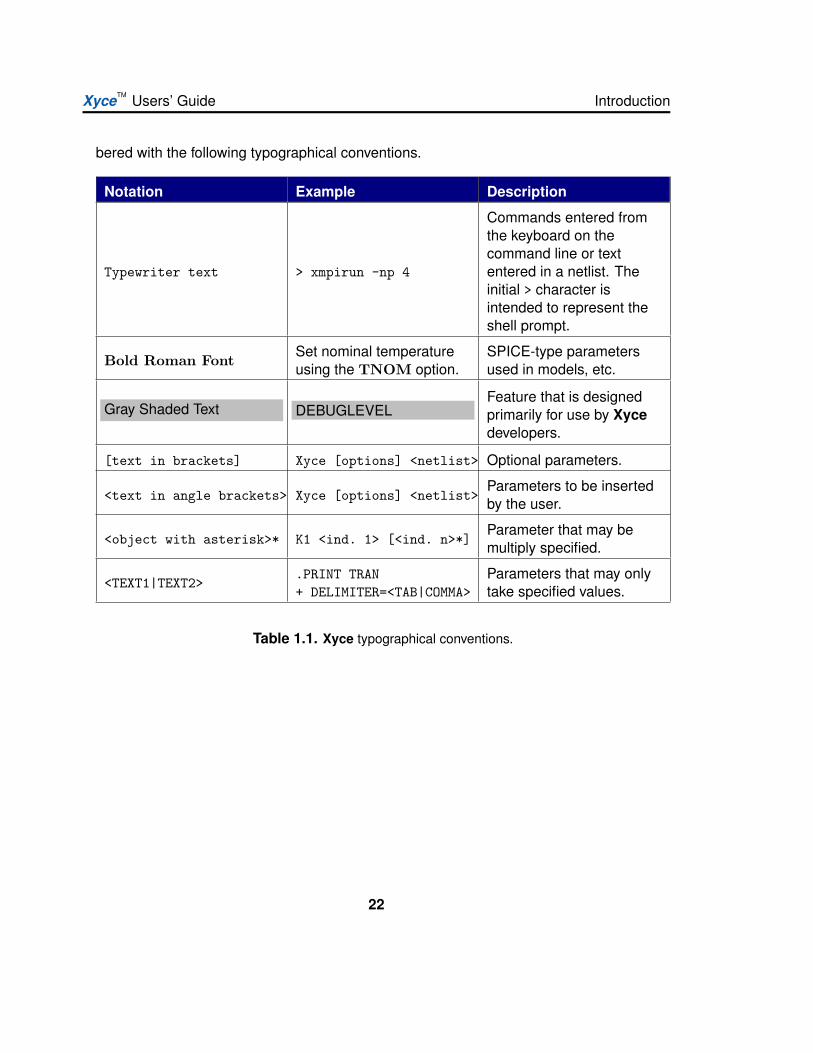
Typographical conventions
Before continuing in this Users’ Guide, it is important to understand the terms and typo-graphical conventions used. Procedures for performing an operation are generally num-
21
XyceTM Users’ Guide Introduction
bered with the following typographical conventions.
Notation Example Description
Typewriter text > xmpirun -np 4
Commands entered fromthe keyboard on thecommand line or textentered in a netlist. Theinitial > character isintended to represent theshell prompt.
Bold Roman FontSet nominal temperatureusing the TNOM option.
SPICE-type parametersused in models, etc.
Gray Shaded Text DEBUGLEVELFeature that is designedprimarily for use by Xycedevelopers.
[text in brackets] Xyce [options] <netlist> Optional parameters.
<text in angle brackets> Xyce [options] <netlist>Parameters to be insertedby the user.
<object with asterisk>* K1 <ind. 1> [<ind. n>*]Parameter that may bemultiply specified.
<TEXT1|TEXT2>.PRINT TRAN+ DELIMITER=<TAB|COMMA>
Parameters that may onlytake specified values.
Table 1.1. Xyce typographical conventions.
22

1.5 Third Party License Information XyceTM Users’ Guide
1.5 Third Party License InformationPortions of the new DAE time integrator contained in the BackwardDifferentiation15 sourceand include files are derived from the IDA code from Lawrence Livermore National Labo-ratories and is licensed under the following license.
Copyright (c) 2002, The Regents of the University of California.Produced at the Lawrence Livermore National Laboratory.Written by Alan Hindmarsh, Allan Taylor, Radu Serban.UCRL-CODE-2002-59All rights reserved.
This file is part of IDA.
Redistribution and use in source and binary forms, with or withoutmodification, are permitted provided that the following conditionsare met:
1. Redistributions of source code must retain the above copyrightnotice, this list of conditions and the disclaimer below.
2. Redistributions in binary form must reproduce the above copyrightnotice, this list of conditions and the disclaimer (as noted below)in the documentation and/or other materials provided with thedistribution.
3. Neither the name of the UC/LLNL nor the names of its contributorsmay be used to endorse or promote products derived from this softwarewithout specific prior written permission.
THIS SOFTWARE IS PROVIDED BY THE COPYRIGHT HOLDERS AND CONTRIBUTORS"AS IS" AND ANY EXPRESS OR IMPLIED WARRANTIES, INCLUDING, BUT NOTLIMITED TO, THE IMPLIED WARRANTIES OF MERCHANTABILITY AND FITNESSFOR A PARTICULAR PURPOSE ARE DISCLAIMED. IN NO EVENT SHALL THEREGENTS OF THE UNIVERSITY OF CALIFORNIA, THE U.S. DEPARTMENT OF ENERGYOR CONTRIBUTORS BE LIABLE FOR ANY DIRECT, INDIRECT, INCIDENTAL,SPECIAL, EXEMPLARY, OR CONSEQUENTIAL DAMAGES (INCLUDING, BUT NOTLIMITED TO, PROCUREMENT OF SUBSTITUTE GOODS OR SERVICES; LOSS OF USE,
23

XyceTM Users’ Guide Introduction
DATA, OR PROFITS; OR BUSINESS INTERRUPTION) HOWEVER CAUSED AND ON ANYTHEORY OF LIABILITY, WHETHER IN CONTRACT, STRICT LIABILITY, OR TORT(INCLUDING NEGLIGENCE OR OTHERWISE) ARISING IN ANY WAY OUT OF THE USEOF THIS SOFTWARE, EVEN IF ADVISED OF THE POSSIBILITY OF SUCH DAMAGE.
Additional BSD Notice---------------------1. This notice is required to be provided under our contract withthe U.S. Department of Energy (DOE). This work was produced at theUniversity of California, Lawrence Livermore National Laboratoryunder Contract No. W-7405-ENG-48 with the DOE.
2. Neither the United States Government nor the University ofCalifornia nor any of their employees, makes any warranty, expressor implied, or assumes any liability or responsibility for theaccuracy, completeness, or usefulness of any information, apparatus,product, or process disclosed, or represents that its use would notinfringe privately-owned rights.
3. Also, reference herein to any specific commercial products,process, or services by trade name, trademark, manufacturer orotherwise does not necessarily constitute or imply its endorsement,recommendation, or favoring by the United States Government or theUniversity of California. The views and opinions of authors expressedherein do not necessarily state or reflect those of the United StatesGovernment or the University of California, and shall not be used foradvertising or product endorsement purposes.
24

2. Installing and RunningXyce
Chapter OverviewThis chapter describes the basic mechanics of installing and running Xyce. It includes thefollowing sections:
Section 2.1, Xyce Installation
Section 2.2, Running Xyce
25

XyceTM Users’ Guide Installing and Running Xyce
2.1 Xyce InstallationTo obtain a copy of Xyce, contact the development team at http://xyce.sandia.gov.
The installation procedure differs depending upon the operating system. Follow the in-structions below to install Xyce.
Installing Xyce on UNIX
Xyce is installed from the command line. Users of Linux, BSD, and other UNIX variantsshould follow this section. Examples are given for reference.
Instructions Examples
Installation packages are namedaccording to the target operating systemand architecture (parallel or serial).
Install_Xyce_Linux.tar.gz (serial)Install_Xyce_Linux_OPENMPI.tar.gz(parallel)
Unpack the appropriate package for yourplatform. A similarly named installationdirectory is then created.
> tar xfz Install_Xyce_Linux.tar
Enter this directory and run theinstallation shell script.
> cd Install_Xyce_Linux> sh install_Linux.sh
Provide the requested information.Where should Xyce be installed?/usr/local/Xyce-5.2
We recommend that you specify a completely new directory in which to install Xyce ratherthan a general system directory. For example, /usr/local/Xyce-5.2 would be a betterchoice than /usr/local. Doing this will help isolate your Xyce installation and make unin-stallation or upgrade easier.
Installing Xyce on Microsoft Windows
Xyce is installed from a self-extracting archive. Run the Install-Xyce.exe program andfollow the on-screen instructions.
26

2.1 Xyce Installation XyceTM Users’ Guide
Important Notes
Completing the steps above will unpack Xyce to the specified directory. IMPORTANTNOTE: if installing both serial and parallel versions of Xyce, you must specify differ-ent directories for each installation location. Failure to use different directories willcause the second installation to overwrite parts of the first and will likely yield aninstall that does not function. Under the specified installation directories, the followingsubdirectories will be created:
bin contains the executable used to start Xyce. The executable name will vary de-pending on the target operating system and architecture.
– runxyce is the shell script for starting serial Xyce on Unix platforms.
– runxyce.bat is the batch file for starting serial Xyce on Windows.
– xmpirun is the wrapper script for mpirun used for running Xyce in parallel mode.
doc contains the Xyce Users’ Guide, comprehensive Reference Guide, and ReleaseNotes. Read these for more information about this release and for detailed instruc-tions on how to use Xyce.
lib contains configuration files, libraries, and metadata for Xyce.
test contains sample netlists and verification tools.
Uninstalling Xyce
For Microsoft Windows, uninstall Xyce using the Control Panel or the Start Menu - Xyce -Uninstall menu option.
For other platforms, Xyce comes with no special uninstall script.
The Xyce installation process simply unpacks a number of files into the directory you iden-tify to the setup program. Removing those files uninstalls Xyce. If you followed our rec-ommendation and installed to a completely separate directory like /usr/local/Xyce-5.2,uninstallation is as simple as removing the entire directory.
27

XyceTM Users’ Guide Installing and Running Xyce
2.2 Running XyceWhile it is possible to connect Xyce to graphical interfaces, such as gEDA [5], this sectiononly describes how Xyce is run from the command line, for both serial and MPI parallelsimulations.
Command Line Simulation
Running Xyce from the command line is straightforward. The scripts xmpirun and runxyceset up the runtime environment and execute Xyce. Help with accessing the command lineon Microsoft Windows is available at the end of this chapter. Depending on whether youare using a version compiled with MPI support or a serial version, there are two ways tobegin running Xyce:
Running serial Xyce:
> runxyce [options] <netlist filename>
Running Xyce in parallel:
> xmpirun -np <# procs> [options] <netlist filename>
where [options] are the command line arguments for Xyce. For example, to log output toa file named sample.log type:
> runxyce -l sample.log <netlist filename>
The next example runs parallel Xyce on four processors and places the results into acomma separated value file named results.csv:
> xmpirun -np 4 -delim COMMA -o results.csv <netlist filename>
These examples assume that <netlist filename> is either in the current working direc-tory or includes the path (full or relative) to the netlist file. Enclose the filename in quotationmarks (” ”) if the path contains spaces. Help is accessible with the -h option.
28

2.2 Running Xyce XyceTM Users’ Guide
For MPI runs, [options] may also include command line arguments to mpirun. Consult thedocumentation installed with MPI on your platform for more details on MPI options. The-np <# procs> denotes the number of processors to use for the simulation. NOTE: It iscritical that the number of processors used is less than the number of devices and voltagenodes in the netlist. The appropriate script used to run Xyce for each supported platformis listed in the Table 2.1.
Architecture OS Serial Executable MPI Executable
x86-64 OSXrunxyce xmpirunx86 and x86-64 Linux
x86 FreeBSD
x86MicrosoftWindows
runxyce.bat not available
Table 2.1. Platform scripts for running Xyce.
While Xyce is running, the progress of the simulation is outputed to the command linewindow.
Command Line Options
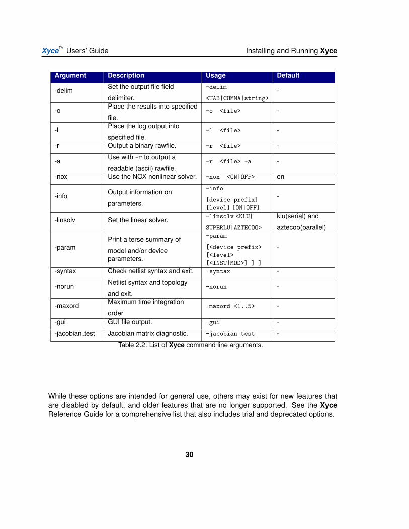
Xyce supports a handful of command line options which must be given before the netlistfilename. The general usage is:
runxyce [options] <netlist filename>
Table 2.2 lists the available command line options.
Argument Description Usage Default
-h Help option. Prints usage and
exits.-h -
-v Prints the version banner and
exits.-v -
29
XyceTM Users’ Guide Installing and Running Xyce
Argument Description Usage Default
-delim Set the output file field
delimiter.
-delim
<TAB|COMMA|string>-
-o Place the results into specified
file.-o <file> -
-l Place the log output into
specified file.-l <file> -
-r Output a binary rawfile. -r <file> -
-a Use with -r to output a
readable (ascii) rawfile.-r <file> -a -
-nox Use the NOX nonlinear solver. -nox <ON|OFF> on
-info Output information on
parameters.
-info
[device prefix][level] [ON|OFF]
-
-linsolv Set the linear solver. -linsolv <KLU|
SUPERLU|AZTECOO>
klu(serial) and
aztecoo(parallel)
-paramPrint a terse summary of
model and/or deviceparameters.
-param
[<device prefix>[<level>[<INST|MOD>] ] ]
-
-syntax Check netlist syntax and exit. -syntax -
-norun Netlist syntax and topology
and exit.-norun -
-maxord Maximum time integration
order.-maxord <1..5> -
-gui GUI file output. -gui -
-jacobian test Jacobian matrix diagnostic. -jacobian_test -
Table 2.2: List of Xyce command line arguments.
While these options are intended for general use, others may exist for new features thatare disabled by default, and older features that are no longer supported. See the XyceReference Guide for a comprehensive list that also includes trial and deprecated options.
30

2.2 Running Xyce XyceTM Users’ Guide
Running Xyce in Parallel
A parallel version of Xyce is available for several different platforms as shown in Table 2.1.Running Xyce in parallel requires the script xmpirun to be used with the appropriate pa-rameters. For example, to run Xyce on two processors with an example netlist, type:
xmpirun -np 2 anExampleNetlist.cir
In general the number of processors is specified by using the -np argument to the appro-priate mpirun command.
Users of Sandia HPC platforms (TLCC, Glory, Red Sky) must set several environmentvariables to run Xyce. A system module is available to handle this. To load the xycemodule, use the command:
module load xyce
Consult the system documentation for help with submitting jobs on these platforms
https://computing.sandia.gov
Guidance
This chapter has given the basic mechanics of running Xyce in parallel. For general guid-ance regarding solver options, partitioning options, and other parallel issues, refer to chap-ter 10. Distributed memory circuit simulation still contains a number of research issues, soobtaining an optimal simulation in parallel is a bit of an art.
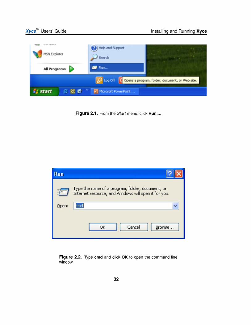
Accessing the Microsoft Windows Command Line
Follow the steps below for help with accessing the command line on Windows XP Profes-sional. Consult the operating system documentation for assistance with other versions ofWindows.
31
XyceTM Users’ Guide Installing and Running Xyce
Figure 2.1. From the Start menu, click Run....
Figure 2.2. Type cmd and click OK to open the command linewindow.
32

2.2 Running Xyce XyceTM Users’ Guide
Figure 2.3. The command line window appears and is ready foruse.
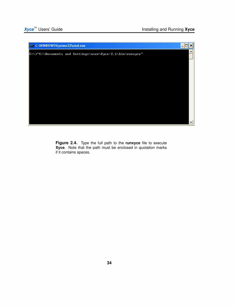
The following is an illustrated recap of the Command Line Simulation instructions providedearlier.
33
XyceTM Users’ Guide Installing and Running Xyce
Figure 2.4. Type the full path to the runxyce file to executeXyce. Note that the path must be enclosed in quotation marksif it contains spaces.
34
2.2 Running Xyce XyceTM Users’ Guide
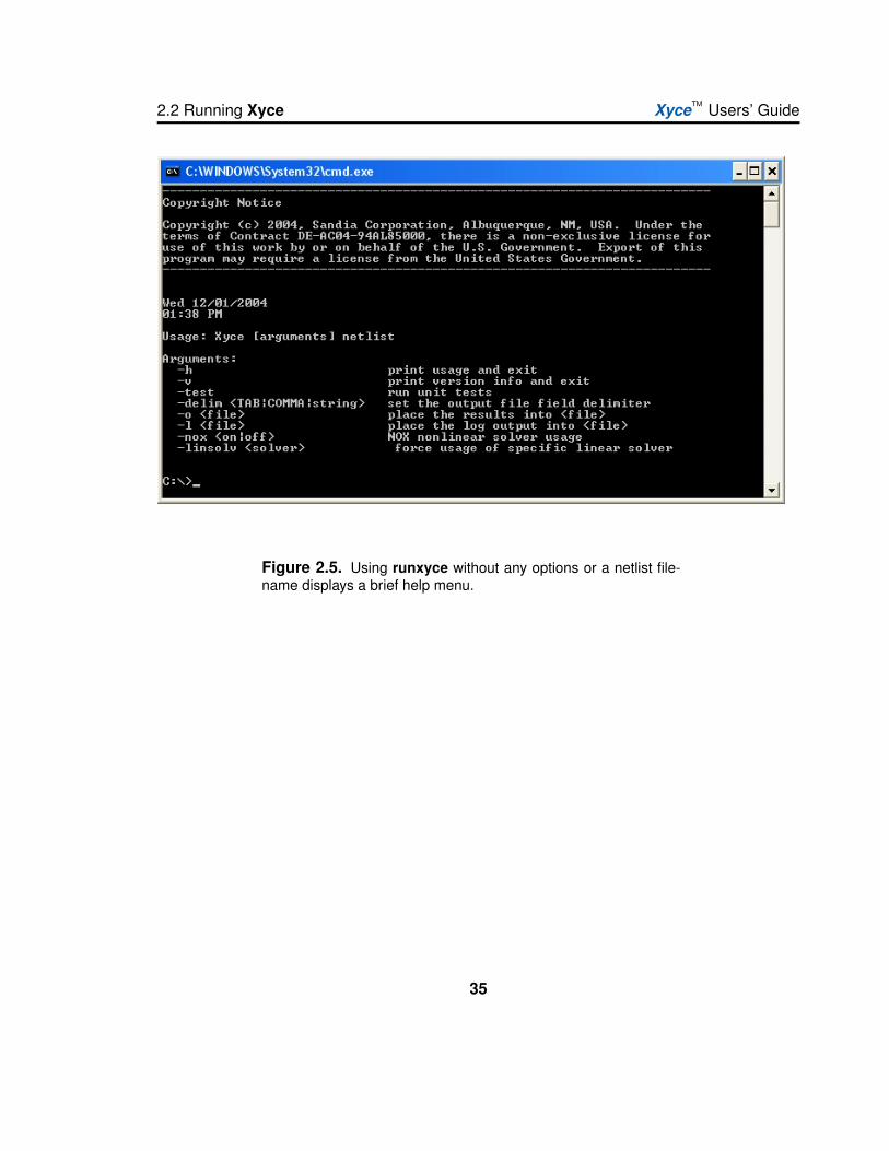
Figure 2.5. Using runxyce without any options or a netlist file-name displays a brief help menu.
35
XyceTM Users’ Guide Installing and Running Xyce
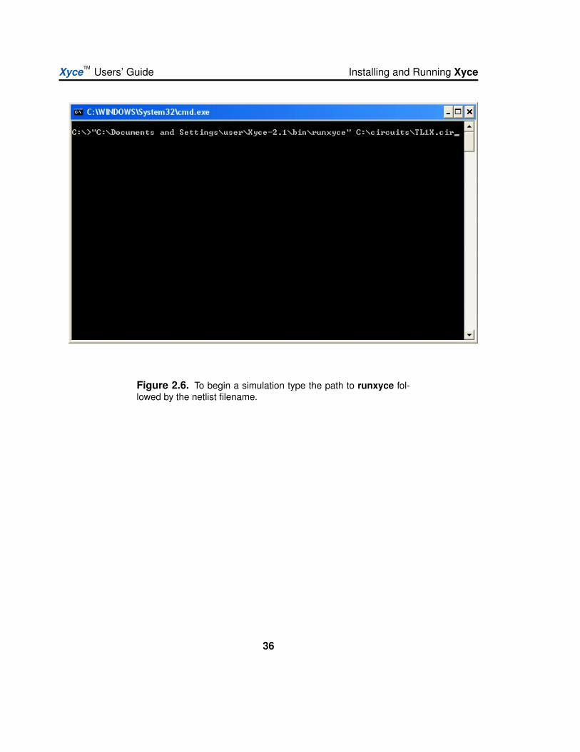
Figure 2.6. To begin a simulation type the path to runxyce fol-lowed by the netlist filename.
36

2.2 Running Xyce XyceTM Users’ Guide
Figure 2.7. Output will scroll to the screen. Use runxyce -h forassistance with command line options.
37

XyceTM Users’ Guide
38
3. Simulation Exampleswith Xyce
Chapter OverviewThis chapter provides several simple examples of Xyce usage. An example circuit is pro-vided for each available analysis type.
Section 3.1, Example Circuit Construction
Section 3.2, DC Sweep Analysis
Section 3.3, Transient Analysis
39
XyceTM Users’ Guide Simulation Examples with Xyce
3.1 Example Circuit Construction
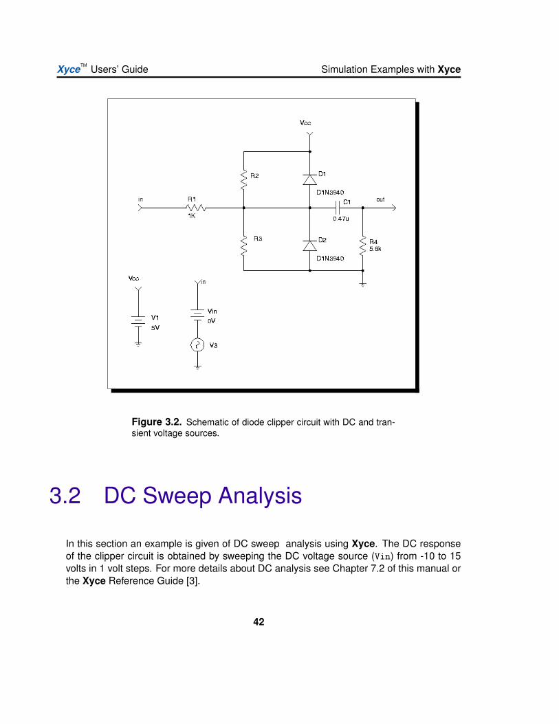
This section describes how to use Xyce to create the simple diode clipper circuit shown inFigure 3.2.
While a schematic edit and capture capability is under development, Xyce currently onlysupports circuit creation via netlist editing. Xyce supports most of the standard netlistentries common to Berkeley SPICE 3F5 and Orcad PSpice. For users who are familiarwith PSpice netlists, the differences between PSpice and Xyce netlists are listed in theXyce Reference Guide [3].
Example: diode clipper circuit
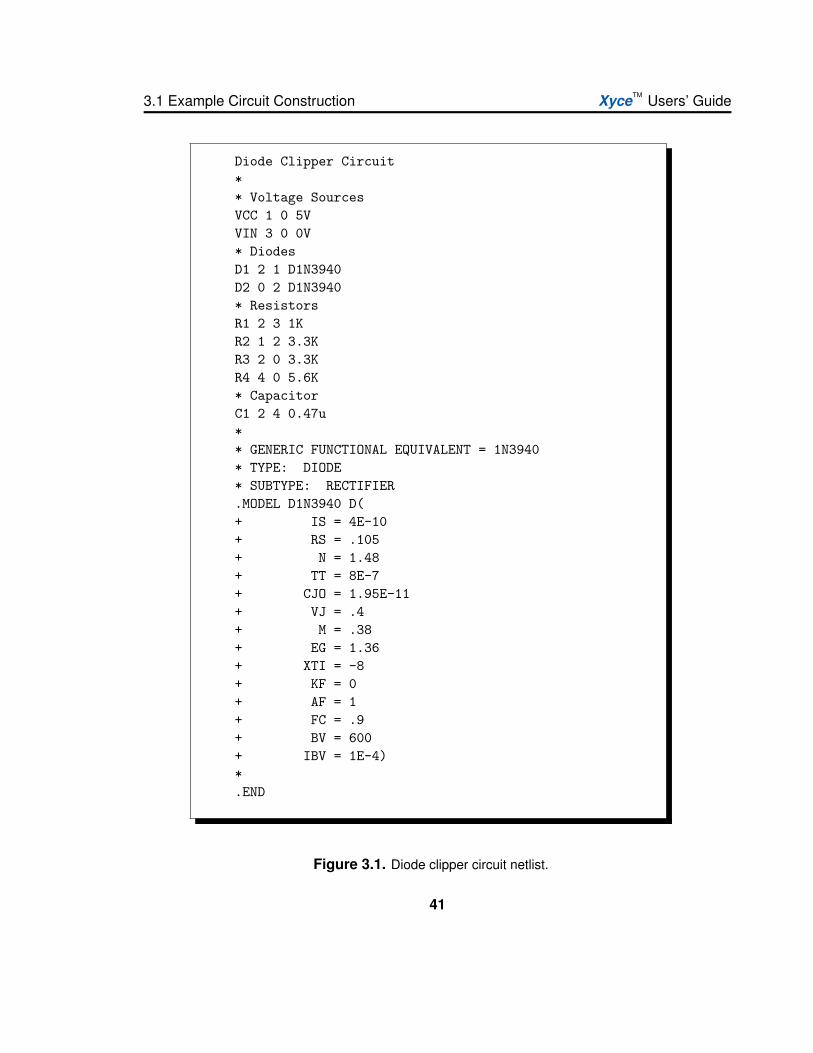
Using a plain text editor of your choice (e.g. vi, emacs, notepad, but not a word processorlike OpenOffice or Microsoft Word), create a file containing the netlist of Figure 3.1. Wewill assume for the rest of this chapter that the file you create is called clipper.cir
The netlist in Figure 3.1 illustrates some of the syntax of a netlist input file. Netlists beginwith a title (e.g. “Diode Clipper Circuit”), support comments (lines beginning with the“*” character), devices, model definitions and the “.END” statement.
The diode clipper circuit contains a number of two-terminal devices (diodes, resistors, andcapacitors), each of which specifies two connecting nodes and either a model (for thediode) or a value (resistance or capacitance). The netlist of Figure 3.1 describes the circuitin the schematic of Figure 3.2
This netlist file is not yet complete and will not run properly using Xyce (see Section 2.2for instructions on running Xyce) as it lacks an analysis statement. As you proceed in thischapter, you will see how to add the appropriate analysis statement and run the clippercircuit.
40
3.1 Example Circuit Construction XyceTM Users’ Guide
Diode Clipper Circuit** Voltage SourcesVCC 1 0 5VVIN 3 0 0V* DiodesD1 2 1 D1N3940D2 0 2 D1N3940* ResistorsR1 2 3 1KR2 1 2 3.3KR3 2 0 3.3KR4 4 0 5.6K* CapacitorC1 2 4 0.47u** GENERIC FUNCTIONAL EQUIVALENT = 1N3940* TYPE: DIODE* SUBTYPE: RECTIFIER.MODEL D1N3940 D(+ IS = 4E-10+ RS = .105+ N = 1.48+ TT = 8E-7+ CJO = 1.95E-11+ VJ = .4+ M = .38+ EG = 1.36+ XTI = -8+ KF = 0+ AF = 1+ FC = .9+ BV = 600+ IBV = 1E-4)*.END
Figure 3.1. Diode clipper circuit netlist.
41
XyceTM Users’ Guide Simulation Examples with Xyce
Figure 3.2. Schematic of diode clipper circuit with DC and tran-sient voltage sources.
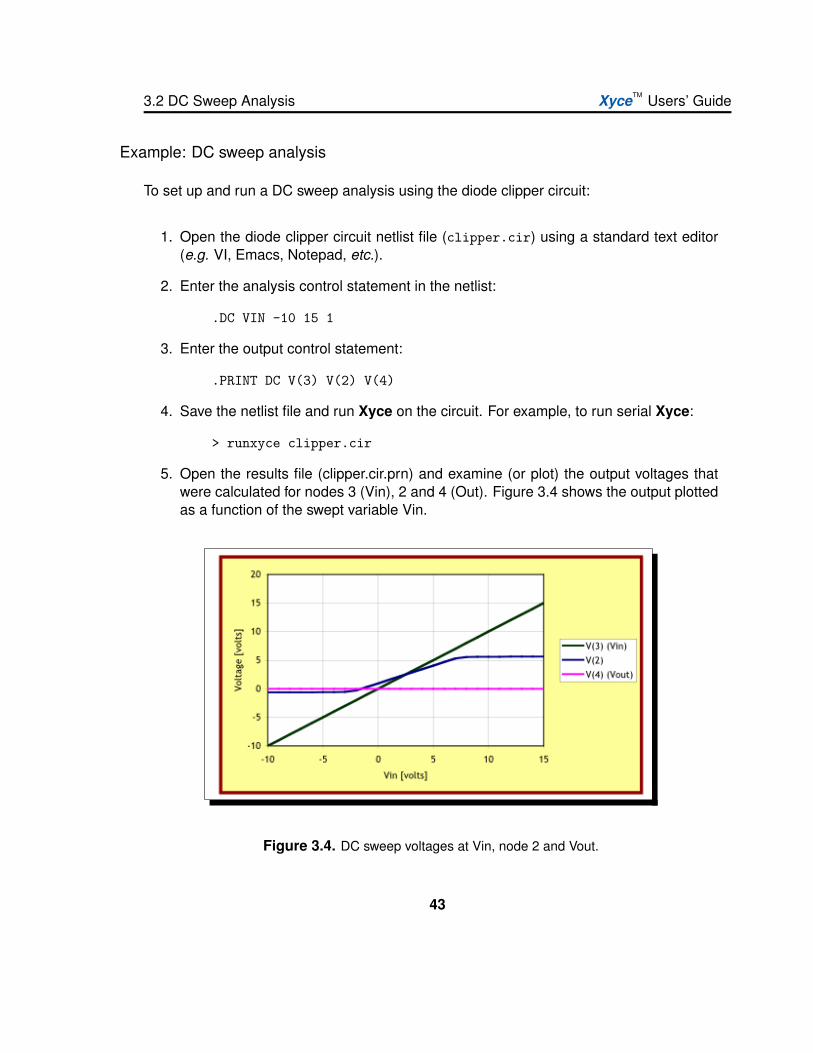
3.2 DC Sweep Analysis
In this section an example is given of DC sweep analysis using Xyce. The DC responseof the clipper circuit is obtained by sweeping the DC voltage source (Vin) from -10 to 15volts in 1 volt steps. For more details about DC analysis see Chapter 7.2 of this manual orthe Xyce Reference Guide [3].
42
3.2 DC Sweep Analysis XyceTM Users’ Guide
Example: DC sweep analysis
To set up and run a DC sweep analysis using the diode clipper circuit:
1. Open the diode clipper circuit netlist file (clipper.cir) using a standard text editor(e.g. VI, Emacs, Notepad, etc.).
2. Enter the analysis control statement in the netlist:
.DC VIN -10 15 1
3. Enter the output control statement:
.PRINT DC V(3) V(2) V(4)
4. Save the netlist file and run Xyce on the circuit. For example, to run serial Xyce:
> runxyce clipper.cir
5. Open the results file (clipper.cir.prn) and examine (or plot) the output voltages thatwere calculated for nodes 3 (Vin), 2 and 4 (Out). Figure 3.4 shows the output plottedas a function of the swept variable Vin.
Figure 3.4. DC sweep voltages at Vin, node 2 and Vout.
43
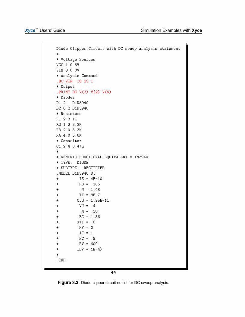
XyceTM Users’ Guide Simulation Examples with Xyce
Diode Clipper Circuit with DC sweep analysis statement** Voltage SourcesVCC 1 0 5VVIN 3 0 0V* Analysis Command.DC VIN -10 15 1* Output.PRINT DC V(3) V(2) V(4)* DiodesD1 2 1 D1N3940D2 0 2 D1N3940* ResistorsR1 2 3 1KR2 1 2 3.3KR3 2 0 3.3KR4 4 0 5.6K* CapacitorC1 2 4 0.47u** GENERIC FUNCTIONAL EQUIVALENT = 1N3940* TYPE: DIODE* SUBTYPE: RECTIFIER.MODEL D1N3940 D(+ IS = 4E-10+ RS = .105+ N = 1.48+ TT = 8E-7+ CJO = 1.95E-11+ VJ = .4+ M = .38+ EG = 1.36+ XTI = -8+ KF = 0+ AF = 1+ FC = .9+ BV = 600+ IBV = 1E-4)*.END
Figure 3.3. Diode clipper circuit netlist for DC sweep analysis.
44
3.3 Transient Analysis XyceTM Users’ Guide
3.3 Transient AnalysisThis section contains an example of transient analysis in Xyce. In this example the DCclipper circuit of the previous section has been modified so that the input voltage source(Vin) is a time-dependent sinusoidal input source. The frequency of Vin is 1 kHz, and hasan amplitude of 10 volts. For more details about transient analysis see Chapter 7.3 of thismanual, or see the Xyce Reference Guide [3].
Example: transient analysis
To set up and run a transient analysis using the diode clipper circuit:
1. Open the diode clipper circuit netlist file file (clipper.cir) using a standard text editor(e.g. VI, Emacs, Notepad, etc.).
2. If you added DC analysis and output statements in the previous example (Figure 3.4),remove them.
3. Enter the analysis control in the netlist:
.TRAN 2ns 2ms
4. Enter the output control statement:
.PRINT TRAN V(3) V(2) V(4)
5. Modify the input voltage source (Vin) to generate the sinusoidal input signal:
VIN 3 0 SIN(0V 10V 1kHz)
6. At this point, the netlist should look similar to the netlist in Figure 3.5. Save the netlistfile and run Xyce on the circuit. For example, to run serial Xyce:
> runxyce clipper.cir
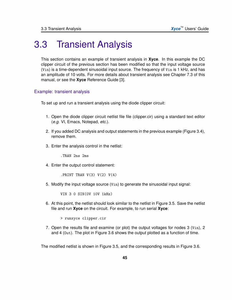
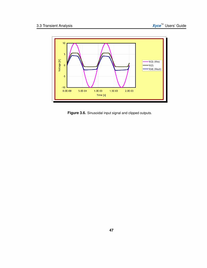
7. Open the results file and examine (or plot) the output voltages for nodes 3 (Vin), 2and 4 (Out). The plot in Figure 3.6 shows the output plotted as a function of time.
The modified netlist is shown in Figure 3.5, and the corresponding results in Figure 3.6.
45

XyceTM Users’ Guide Simulation Examples with Xyce
Diode Clipper Circuit with transient analysis statement** Voltage SourcesVCC 1 0 5VVIN 3 0 SIN(0V 10V 1kHz)* Analysis Command.TRAN 2ns 2ms* Output.PRINT TRAN V(3) V(2) V(4)* DiodesD1 2 1 D1N3940D2 0 2 D1N3940* ResistorsR1 2 3 1KR2 1 2 3.3KR3 2 0 3.3KR4 4 0 5.6K* CapacitorC1 2 4 0.47u** GENERIC FUNCTIONAL EQUIVALENT = 1N3940* TYPE: DIODE* SUBTYPE: RECTIFIER.MODEL D1N3940 D(+ IS = 4E-10+ RS = .105+ N = 1.48+ TT = 8E-7+ CJO = 1.95E-11+ VJ = .4+ M = .38+ EG = 1.36+ XTI = -8+ KF = 0+ AF = 1+ FC = .9+ BV = 600+ IBV = 1E-4)*.END
Figure 3.5. Diode clipper circuit netlist for transient analysis.
46
3.3 Transient Analysis XyceTM Users’ Guide
Figure 3.6. Sinusoidal input signal and clipped outputs.
47

XyceTM Users’ Guide
48
4. Netlist Basics
Chapter OverviewThis chapter contains introductory material on netlist syntax and usage. Sections include:
Section 4.1 General Overview
Section 4.2 Devices Available for Simulation
Section 4.3 Parameters and Expressions
49

XyceTM Users’ Guide Netlist Basics
4.1 General Overview
Introduction
Using a netlist to describe a circuit for Xyce is the primary method for running a circuitsimulation. Netlist support within Xyce largely conforms to that used by Berkeley SPICE3F5 with several new options for controlling functionality unique to Xyce. In a netlist, thecircuit is described by a set of element lines which define the circuit elements, their values,the circuit topology (i.e. the connection of the circuit elements), and a variety of controloptions for the simulation. The first line in the netlist file must be a title and the last linemust be “.END”. Between these two constraints, the order of the statements is irrelevant.
Nodes
Nodes and elements form the foundation for the circuit topology. Each node represents apoint in the circuit that is connected to the leads of multiple elements (devices). Each leadof every element is connected to a node, and each node is connected to multiple elementleads.
A node is simply a named point in the circuit. The naming of normal nodes is only knownwithin the level of circuit hierarchy where they appear; normal nodes defined in the maincircuit are not visible to subcircuits, nor are nodes defined in a subcircuit visible to the top-level circuit. Nodes can be passed into subcircuits through an argument list, and in thiscase subcircuits are given limited access to nodes from the upper-level circuit.
Global Nodes
For cases where a particular node is used widely throughout various subcircuits it can bemore convenient to use a global node, which is referenced by the same name throughoutthe circuit. This is often the case for power rails such as VDD or VSS.
Global nodes start with the prefix $G. Examples of global node names would be: $G VDDor $G1. There is no declaration required for nodes or global nodes. They are declaredimplicitly by appearing in element lines.
50

4.1 General Overview XyceTM Users’ Guide
Elements
An element line, for which the format is determined by the specific element type, defineseach circuit element instance. The general format is given by:
<type><name> <node information> <element information...>
The <type> must be a letter (A through Z) and the <name> follows immediately. For ex-ample, RARESISTOR specifies a device of type “R” (for “Resistor”) with a name ARESISTOR.Nodes are separated by spaces, and additional element information required by the deviceis given after the node list as described in the Netlist Reference section of the Xyce Refer-ence Guide [3]. Xyce ignores character case when reading a netlist such that RARESISTORis equivalent to raresistor. The only exception to this case insensitivity occurs when in-cluding external files in a netlist where the filename specified in the netlist must have thesame case as the actual filename.
A number field may be an integer or a floating-point value. Either one may be followed byone of the following scaling factors:
Symbol Equivalent Value
T 1012
G 109
Meg 106
K 103
mil 25.4−6
m 10−3
u (µ) 10−6
n 10−9
p 10−12
f 10−15
Node information is given in terms of node names, which are arbitrary character strings.The only requirement is that the ground node is named ’0’. There are some restrictions onthe circuit topology:
51

XyceTM Users’ Guide Netlist Basics
There can be no loop of voltage sources and/or inductors.
There can be no cut-set of current sources and/or capacitors.
In addition to these two requirements, the following additional topology constraints arehighly recommended:
Every node has a DC path to ground.
Every node has at least two connections (with the exception of unterminated trans-mission lines and MOSFET substrate nodes).
While Xyce can theoretically handle netlists which violate the above two constraints, suchtopologies are typically the result of human error in creating a netlist file and will often leadto convergence failures. See Chapter 14 of this guide for more on this topic.
The following line provides an example of an element line that defines a resistor betweennodes 1 and 3 with a resistance value of 10kΩ.
Example: RARESISTOR 1 3 10K
Title, Comments and End
The first line of the netlist is the title line of the netlist. This line is treated as a commenteven if it does not begin with an asterisk. It is a common mistake to forget the meaning ofthis first line and begin the circuit elements on the first line; doing so will probably result ina parsing error.
Example: Test RLC Circuit
The “.END” line must be the last line in the netlist.
Example: .END
Comments are supported in netlists and are indicated by placing an asterisk at the be-ginning of the comment line. They may occur anywhere in the netlist but they must beat the beginning of a line. Xyce also supports in-line comments. An in-line comment isdesignated by a semicolon and may occur on any line. Everything after the semicolon is
52

4.1 General Overview XyceTM Users’ Guide
taken as a comment and ignored. Any line that begins with leading white space is alsoconsidered to be a comment.
Example: * This is a netlist comment.
Example: WRONG:.DC .... * This type of in-line comment is not supported.
Example: .DC .... ; This type of in-line comment is supported.
Continuation Lines
Any line that begins with a + symbol is a continuation line. Its contents are appended tothose of the previous line. If the previous line or lines were comments, the continuation lineis appended to the first non-comment line preceding it.
Netlist Commands
Command elements are used to describe the analysis being defined by the netlist. Exam-ples include analysis types, initial conditions, device models and output control. The XyceReference Guide [3] contains a reference for these commands.
Example: .PRINT TRAN V(Vout)
Analog Devices
The analog devices supported include most of the standard circuit components normallyfound in circuit simulators such as SPICE 3F5, PSpice, etc., plus several Sandia specificdevices.
Example: D CR303 N 0065 0 D159700
To find out more about analog devices see the Xyce Reference Guide [3].
53
XyceTM Users’ Guide Netlist Basics
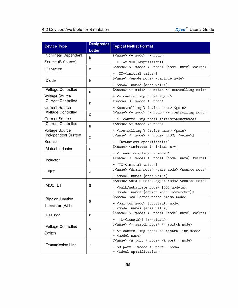
4.2 Devices Available for SimulationThis section describes the different types of analog devices supported in Xyce. Theseinclude standard analog devices, sources (dependent and independent) and subcircuits.Each device description has the following information:
A description and an example of the netlist syntax
The corresponding model types and descriptions, where applicable
The corresponding lists of model parameters and descriptions, where applicable
The associated circuit diagram and model equations, as necessary
These analog devices include all of the standard circuit components needed for most ana-log circuits. User defined models may also be implemented using the .MODEL (modeldefinition) statement and macromodels as subcircuits using the .SUBCKT (subcircuit) state-ment.
Analog Devices
Xyce supports many analog devices, including sources, subcircuits and behavioral mod-els. The devices are classified into device types, each of which can have one or moremodel types. For example, the BJT device type has two model types: NPN and PNP.
The device element statements in the netlist always start with the name of the individualdevice instance. The first letter of the name determines the device type. The format ofthe following information depends on the device type and its parameters. The Device Typesummary table, Table 4.1, lists all of the analog devices supported by Xyce. Each standarddevice is then described in more detail in the following sections. Except where noted, thedevices are based upon those found in [6].
Table 4.1 is a summary of the analog device types and the form of their netlist formats. Fora more complete description of the syntax for supported devices, see the Xyce ReferenceGuide. [3].
54
4.2 Devices Available for Simulation XyceTM Users’ Guide
Device Type Designator
LetterTypical Netlist Format
Nonlinear Dependent
Source (B Source)B
B<name> <+ node> <- node>
+ <I or V>=<expression>
Capacitor CC<name> <+ node> <- node> [model name] <value>
+ [IC=<initial value>]
Diode DD<name> <anode node> <cathode node>
+ <model name> [area value]Voltage Controlled
Voltage SourceE
E<name> <+ node> <- node> <+ controlling node>
+ <- controlling node> <gain>Current Controlled
Current SourceF
F<name> <+ node> <- node>
+ <controlling V device name> <gain>Voltage Controlled
Current SourceG
G<name> <+ node> <- node> <+ controlling node>
+ <- controlling node> <transconductance>Current Controlled
Voltage SourceH
H<name> <+ node> <- node>
+ <controlling V device name> <gain>Independent Current
SourceI
I<name> <+ node> <- node> [[DC] <value>]
+ [transient specification]
Mutual Inductor KK<name> <inductor 1> [<ind. n>*]
+ <linear coupling or model>
Inductor LL<name> <+ node> <- node> [model name] <value>
+ [IC=<initial value>]
JFET JJ<name> <drain node> <gate node> <source node>
+ <model name> [area value]
MOSFET MM<name> <drain node> <gate node> <source node>
+ <bulk/substrate node> [SOI node(s)]+ <model name> [common model parameter]*
Bipolar Junction
Transistor (BJT)Q
Q<name> <collector node> <base node>
+ <emitter node> [substrate node]+ <model name> [area value]
Resistor RR<name> <+ node> <- node> [model name] <value>
+ [L=<length>] [W=<width>]
Voltage Controlled
SwitchS
S<name> <+ switch node> <- switch node>
+ <+ controlling node> <- controlling node>+ <model name>
Transmission Line TT<name> <A port + node> <A port - node>
+ <B port + node> <B port - node>+ <ideal specification>
55
XyceTM Users’ Guide Netlist Basics
Device Type Designator
LetterTypical Netlist Format
Independent Voltage
SourceV
V<name> <+ node> <- node> [[DC] <value>]
+ [transient specification]
Subcircuit XX<name> [node]* <subcircuit name>
+ [PARAMS:[<name>=<value>]*]Current Controlled
SwitchW
W<name> <+ switch node> <- switch node>
+ <controlling V device name> <model name>Digital Devices Y<name> Y<name> [node]* <model name>
PDE Devices YPDE YPDE <name> [node]* <model name>
ROM Devices YROM YROM <name> <+ node> <- node>
+ BASE_FILENAME=<filename>
+ [MASK_VARS=<true/false>]
MESFET ZZ<name> <drain node> <gate node> <source node>
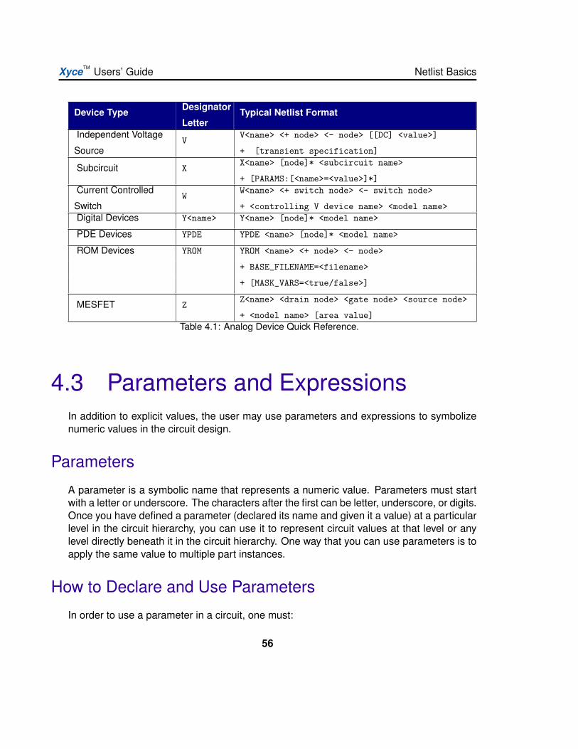
+ <model name> [area value]Table 4.1: Analog Device Quick Reference.
4.3 Parameters and ExpressionsIn addition to explicit values, the user may use parameters and expressions to symbolizenumeric values in the circuit design.
Parameters
A parameter is a symbolic name that represents a numeric value. Parameters must startwith a letter or underscore. The characters after the first can be letter, underscore, or digits.Once you have defined a parameter (declared its name and given it a value) at a particularlevel in the circuit hierarchy, you can use it to represent circuit values at that level or anylevel directly beneath it in the circuit hierarchy. One way that you can use parameters is toapply the same value to multiple part instances.
How to Declare and Use Parameters
In order to use a parameter in a circuit, one must:
56
4.3 Parameters and Expressions XyceTM Users’ Guide
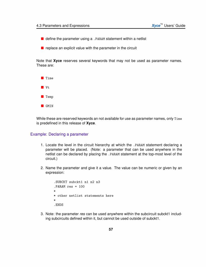
define the parameter using a .PARAM statement within a netlist
replace an explicit value with the parameter in the circuit
Note that Xyce reserves several keywords that may not be used as parameter names.These are:
Time
Vt
Temp
GMIN
While these are reserved keywords an not available for use as parameter names, only Timeis predefined in this release of Xyce.
Example: Declaring a parameter
1. Locate the level in the circuit hierarchy at which the .PARAM statement declaring aparameter will be placed. (Note: a parameter that can be used anywhere in thenetlist can be declared by placing the .PARAM statement at the top-most level of thecircuit.)
2. Name the parameter and give it a value. The value can be numeric or given by anexpression:
.SUBCKT subckt1 n1 n2 n3
.PARAM res = 100** other netlist statements here*.ENDS
3. Note: the parameter res can be used anywhere within the subcircuit subckt1 includ-ing subcircuits defined within it, but cannot be used outside of subckt1.
57

XyceTM Users’ Guide Netlist Basics
Example: Using a parameter in the circuit
1. Find the numeric value that is to be replaced by a parameter: a device instanceparameter value, model parameter value, etc. The value being replaced must beaccessible with the current hierarchy level.
2. Replace the numeric value with the parameter name contained within braces () asin:
R1 1 2 res
Limitations on parameter definitions
There is considerable flexibility in the use of parameters, as described in section 6, analogbehavioral modelling. Parameters can be set to expressions containing other parameters,and can be passed down the heirarchy into subcircuits. Fundamentally, however, parame-ters are constants that are evaluated at the beginning of a run. All terms in the expressiondefining the parameter must therefore be constants known at the beginning of the run. Itis not legal to use any time-dependent expressions in parameter declarations (either byincluding voltage nodes or currents, or by including reference to the variable TIME).
If a parameter is defined within a given scope then it can be used in any expression withinthat scope. The only limitation on ordering is for the use of a parameter in an expressionthat defines the value of another parameter. In that case, all parameters used in the expres-sion must be defined before being used to define another parameter. So,in the followingexample:
R1 1 0 B+C ; OK because the expression is not used to define a param.PARAM A=3.PARAM B=A+1 ; OK because A is defined above.PARAM D=C+2 ; Illegal because C is not yet known.PARAM C=2
Global Parameters
A normal parameter that is defined at the main circuit level will have global scope. Suchparameter suffer from limitations that (1) they are constant during the simulation, and (2)the parameter may redefined within a subcircuit, which would change the value in thesubcircuit and below. Global parameters address these limitations.
58
4.3 Parameters and Expressions XyceTM Users’ Guide
A global parameter differs from a normal parameter in that is can only be defined at themain circuit level, and it is allowed to change during a simulation. It acts like a variablerather than a constant during the simulation. An example of some global parameter usagesare:
.param dTdt=100
.global_param T=27+dTdt*timeR1 1 2 RMOD TEMP=T
or . .
.global_param T=27R1 1 2 RMOD TEMP=TC1 1 2 CMOD TEMP=T.step T 20 50 10
In these examples, T is used to represent an environmental variable that changes.
Note that normal parameters may be used in expressions that define global parameters,but the the opposite is not allowed.
Expressions
In Xyce, an expression is a mathematical relationship that may be used any place onewould use a number (numeric or boolean). Except in the case of expressions used inanalog behavioral modeling sources (see Chapter 6) Xyce evaluates the expression to avalue when it reads in the circuit netlist, not each time its value is needed. It is thereforenecessary that all terms in an expression be known at the beginning of the run.
To use an expression in a circuit netlist:
1. Locate the value to be replaced (component, model parameter, etc.).
2. Substitute the value with an expression utilizing the syntax:
expression
where expression can contain any of the following:
available operators from those in Table 4.2
59

XyceTM Users’ Guide Netlist Basics
included functions from those in Table 4.3, Table 4.5, and Table 4.6
user-defined functions
user-defined parameters that are within scope
literal operands
The braces () instruct Xyce to evaluate the expression and use the resulting value.
Additional time-dependent constructs are available in expressions used in analogbehavioral modeling sources (see Chapter 6).
Example: Using an expression
Scaling the DC voltage of a 12V independent voltage source, designated VF, by somefactor can be accomplished by the following netlist statements (in this example the factoris 1.5):
.PARAM FACTORV=1.5VF 3 4 FACTORV*12
Xyce will evaluate the expression to 12 ∗ 1.5 or 18 volts.
1Logical and relational operators are used only with the IF() function.
60
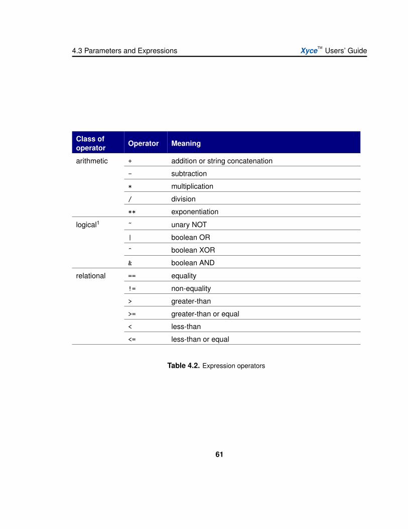
4.3 Parameters and Expressions XyceTM Users’ Guide
Class ofoperator Operator Meaning
arithmetic + addition or string concatenation
- subtraction
* multiplication
/ division
** exponentiation
logical1 ~ unary NOT
| boolean OR
^ boolean XOR
& boolean AND
relational == equality
!= non-equality
> greater-than
>= greater-than or equal
< less-than
<= less-than or equal
Table 4.2. Expression operators
61
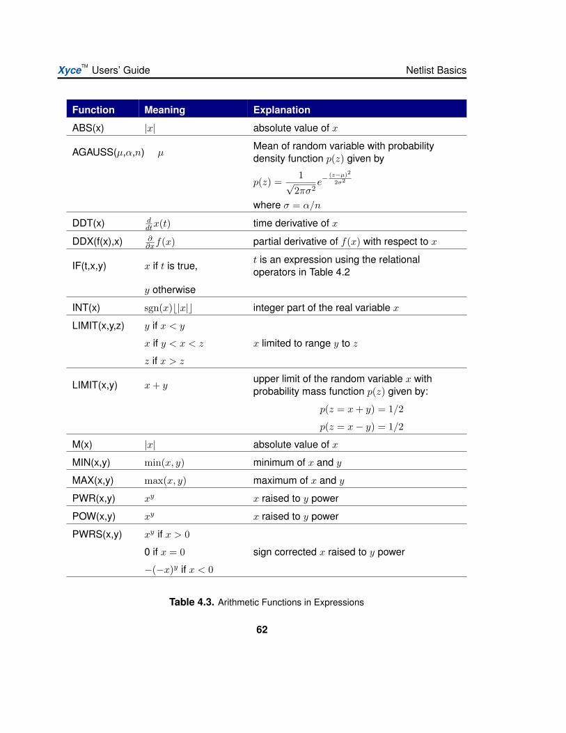
XyceTM Users’ Guide Netlist Basics
Function Meaning Explanation
ABS(x) |x| absolute value of x
AGAUSS(µ,α,n) µMean of random variable with probabilitydensity function p(z) given by
p(z) =1√
2πσ2e−
(z−µ)2
2σ2
where σ = α/n
DDT(x) ddtx(t) time derivative of x
DDX(f(x),x) ∂∂xf(x) partial derivative of f(x) with respect to x
IF(t,x,y) x if t is true,t is an expression using the relationaloperators in Table 4.2
y otherwise
INT(x) sgn(x)b|x|c integer part of the real variable x
LIMIT(x,y,z) y if x < y
x if y < x < z x limited to range y to z
z if x > z
LIMIT(x,y) x + yupper limit of the random variable x withprobability mass function p(z) given by:
p(z = x + y) = 1/2
p(z = x− y) = 1/2
M(x) |x| absolute value of x
MIN(x,y) min(x, y) minimum of x and y
MAX(x,y) max(x, y) maximum of x and y
PWR(x,y) xy x raised to y power
POW(x,y) xy x raised to y power
PWRS(x,y) xy if x > 0
0 if x = 0 sign corrected x raised to y power
−(−x)y if x < 0
Table 4.3. Arithmetic Functions in Expressions
62

4.3 Parameters and Expressions XyceTM Users’ Guide
Function Meaning Explanation
RAND() 0 < result < 1 random constant number between 0 and 1
SDT(x)∫
x(t)dt time integral of x
SGN(x) +1 if x > 0
0 if x = 0 sign value of x
-1 if x < 0
SIGN(x,y) sgn(y)|x| Sign of y times absolute value of x
STP(x) 1 if x > 0 step function
0 otherwise
SQRT(x)√
x square root of x
TABLE(x,y,z,*) f(x) where f(y) = zpiecewise linear interpolation, multiple (y,z)pairs can be specified
URAMP(x) x if x > 0 ramp function
0 otherwise
Table 4.4. Arithmetic Functions in Expressions (cont’d)
63

XyceTM Users’ Guide Netlist Basics
Function Meaning Explanation
ACOS(x) arccos(x) result in radians
ACOSH(x) cosh−1(x) hyperbolic arccosine of x
ARCTAN(x) arctan(x) result in radians
ASIN(x) arcsin(x) result in radians
ASINH(x) sinh−1(x) hyperbolic arcsine of x
ATAN(x) arctan(x) result in radians
ATANH(x) tanh−1(x) hyperbolic arctangent of x
ATAN2(x,y) arctan(x/y) result in radians
COS(x) cos(x) x in radians
COSH(x) cosh(x) hyperbolic cosine of x
EXP(x) ex e to the x power
LN(x) ln(x) log base e
LOG(x) log(x) log base 10
LOG10(x) log(x) log base 10
SIN(x) sin(x) x in radians
SINH(x) sinh(x) hyperbolic sine of x
TAN(x) tan(x) x in radians
TANH(x) tanh(x) hyperbolic tangent of x
Table 4.5. Exponential, Logarithmic, and Trigonometric Func-tions in Expressions
64
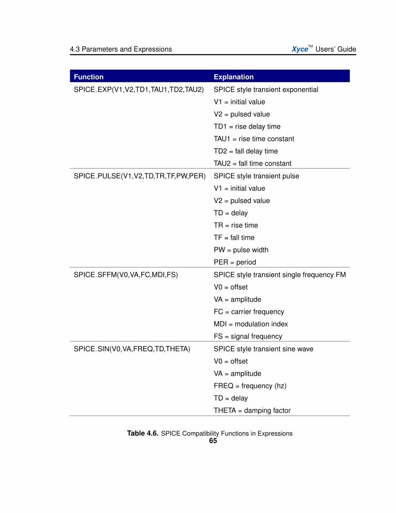
4.3 Parameters and Expressions XyceTM Users’ Guide
Function Explanation
SPICE EXP(V1,V2,TD1,TAU1,TD2,TAU2) SPICE style transient exponential
V1 = initial value
V2 = pulsed value
TD1 = rise delay time
TAU1 = rise time constant
TD2 = fall delay time
TAU2 = fall time constant
SPICE PULSE(V1,V2,TD,TR,TF,PW,PER) SPICE style transient pulse
V1 = initial value
V2 = pulsed value
TD = delay
TR = rise time
TF = fall time
PW = pulse width
PER = period
SPICE SFFM(V0,VA,FC,MDI,FS) SPICE style transient single frequency FM
V0 = offset
VA = amplitude
FC = carrier frequency
MDI = modulation index
FS = signal frequency
SPICE SIN(V0,VA,FREQ,TD,THETA) SPICE style transient sine wave
V0 = offset
VA = amplitude
FREQ = frequency (hz)
TD = delay
THETA = damping factor
Table 4.6. SPICE Compatibility Functions in Expressions65

XyceTM Users’ Guide
66
5. Working with .MODELStatements and SubcircuitModels
Chapter OverviewThis chapter contains model ideas and a summary of the ways to create and modify mod-els. Sections include:
Section 5.1, Definition of a Model
Section 5.2, Model Organization
67
XyceTM Users’ Guide Working with .MODEL Statements and Subcircuit Models
5.1 Definition of a Model
A model describes the electrical performance of a part, such as a specific vendor’s versionof a 2N2222 transistor. To simulate a part requires specification of simulation properties.These properties define the model of the part.
Depending on the given device type and the requirements of the circuit design, a model isspecified using a model parameter set, a subcircuit netlist, or both.
In general, model parameter sets define the parameters used in ideal models of specificdevice types, and subcircuit netlists allow the user to combine ideal device models to sim-ulate more complex effects. For example, one could simulate a bipolar transistor using theXyce BJT device by specifying model parameters extracted to fit the simulation behavior tothe behavior of the part used, or one could develop a subcircuit macro-model of a capacitorthat adds effects like lead inductance and resistance to the basic capacitor device.
Both methods of defining a model use a netlist format, with precise syntax rules as de-scribed below.
Defining models using model parameters
Xyce currently has no built-in part models. However, models can be defined for a device bychanging some or all of the model parameters from their defaults via the .MODEL statement.For example:
M5 3 2 1 0 MLOAD1.MODEL MLOAD1 NMOS (LEVEL=3 VTO=0.5 CJ=0.025pF)
This example defines a MOSFET device M5 that is an instance of a part described bythe model parameter set MLOAD1. The MLOAD1 parameter set is defined in the .MODELstatement.
Most device types in Xyce support some form of model parameters. Consult the XyceReference Guide [3] for the model parameters supported by each device type.
68

5.1 Definition of a Model XyceTM Users’ Guide
Defining models using subcircuit netlists
In Xyce, models may also be defined using the subcircuit syntax: .SUBCKT/.ENDS. Thissyntax includes:
netlists to define the configuration and function of the part.
variable input parameters to modify the model.
See Figure 5.1 for an example.
****other devicesX5 5 6 7 8 l3dsc1 PARAMS: ScaleFac=2.0X6 9 10 11 12 l3dsc1****more netlist commands
*** SUBCIRCUIT: l3dsc1*** Parasitic Model: microstrip*** Only one segment.SUBCKT l3dsc1 1 3 2 4 PARAMS: ScaleFac=1.0C01 1 0 4.540e-12RG01 1 0 7.816e+03L1 1 5 3.718e-08R1 5 2 4.300e-01C1 2 0 4.540e-12RG1 2 0 7.816e+03C02 3 0 4.540e-12RG02 3 0 7.816e+03L2 3 6 3.668e-08R2 6 4 4.184e-01C2 4 0 4.540e-12RG2 4 0 7.816e+03CM012 1 3 5.288e-13KM12 L1 L2 2.229e-01CM12 2 4 5.288e-13*ScaleFac.ENDS
Figure 5.1. Example subcircuit model.
69
XyceTM Users’ Guide Working with .MODEL Statements and Subcircuit Models
In this example, a subcircuit model called l3dsc1 implementing one part of a microstriptransmission line is defined between the .SUBCKT/.ENDS lines, and two different instancesof the subcircuit are used in the X lines. This somewhat artificial example shows how inputparameters are used; the last capacitor in the subcircuit is scaled by the input parameterScaleFac. If input parameters are not specified on the X line (as in the case of device X6),then the default values specified on the .SUBCKT line are used. Non-default values arespecified on the X line using the PARAMS: keyword. For precise syntax consult the XyceReference Guide [3].
Subcircuit Hierarchy
Xyce supports the definition of subcircuits within other subcircuits. Each subcircuit defini-tion introduces a new level in the circuit hierarchy with the top level being the main circuit. Ifa second level is defined, it is composed of the subcircuits in the main circuit and each sub-sequent level is composed of the subcircuits contained in the previous level. A subcircuitmay also contain other definitions such as models via the .MODEL statement, parametersvia the .PARAM statement, and functions via the .FUNC statement.
In this context, the subcircuit defines the “scope” for the definitions it contains. That is,the definitions contained within a subcircuit can be used within that subcircuit and/or withinany subcircuit it contains. Any definitions occurring in the main circuit have global scopeand can be used anywhere in the circuit. A name, such as a model, parameter, function orsubcircuit name, occurring in a definition at one level of a circuit hierarchy can be redefinedat any lower level contained directly by the subcircuit. In this case, the new definitionapplies at the given level and those below.
In the following example, the model named MOD1 can be used in subcircuits SUB1 and SUB2but not in the subcircuit SUB3. The parameter P1 has a value of 10 in subcircuit SUB1 and avalue of 20 in subcircuit SUB2.
70

5.1 Definition of a Model XyceTM Users’ Guide
.SUBCKT SUB1 1 2 3 4
.MODEL MOD1 NMOS(LEVEL=2)
.PARAM P1=10** subcircuit devices omitted for brevity*.SUBCKT SUB2 1 3 2 4.PARAM P1=20** subcircuit devices omitted for brevity*.ENDS.ENDS
.SUBCKT SUB3 1 2 3 4** subcircuit devices omitted for brevity*.ENDS
Figure 5.2. Example subcircuit model.
71
XyceTM Users’ Guide Working with .MODEL Statements and Subcircuit Models
5.2 Model OrganizationWhile it is always possible to make a self-contained netlist in which all models for allparts are included along with the circuit definition, it is often more convenient to orga-nize frequently-used models into separate model libraries. Xyce provides a very simplemechanism that allows this organization. Models are simply collected into model libraryfiles, and then accessed by netlists as needed by insertion of an .INCLUDE directive. Thissection describes the process in detail.
Model libraries
Device model and subcircuit definitions may be organized into model libraries. Theselibraries are text files (similar to netlist files) that have one or more model definitions. Manyusers choose to give model library files names that end with .lib, but the file may benamed using any convention the user chooses.
In general, most users create model libraries files that typically include similar model types.In these files, the header comments describe the models therein.
Model library configuration
In Xyce, model libraries are used by inserting a .INCLUDE statement into a netlist. Oncea file is included, its contents are available to the netlist just as if the entire contents hadbeen inserted directly into the netlist.
As an example, one might create the following model library file called bjtmodels.lib,containing .MODEL statements for common types of bipolar junction transistors:
*bjtmodels.lib* Bipolar transistor models.MODEL Q2N2222 NPN (Is=14.34f Xti=3 Eg=1.11 Vaf=74.03 Bf=5 Ne=1.307+ Ise=14.34f Ikf=.2847 Xtb=1.5 Br=6.092 Nc=2 Isc=0 Ikr=0 Rc=1+ Cjc=7.306p Mjc=.3416 Vjc=.75 Fc=.5 Cje=22.01p Mje=.377 Vje=.75+ Tr=46.91n Tf=411.1p Itf=.6 Vtf=1.7 Xtf=3 Rb=10)
.MODEL 2N3700 NPN (IS=17.2E-15 BF=100)
.MODEL 2N2907A PNP (IS=1.E-12 BF=100)
72

5.2 Model Organization XyceTM Users’ Guide
The models Q2N2222, 2N3700 and 2N2907A could then be used in a netlist by including thebjtmodels.lib file.
.INCLUDE "bjtmodels.lib"Q1 1 2 3 Q2N2222Q2 5 6 7 2N3700Q3 8 9 10 2N2907A*other netlist entries.END
Because the contents of an included file are simply inserted into the netlist at the pointwhere the .INCLUDE statement appears, the scoping rules for .INCLUDE statements is thesame as for other types of definitions as outlined in the preceding section. Note that thepath to the library file is assumed to be relative to the execution directory, but absolutepathnames are permissible. Note also that the entire file name, including its “extension”must be specified. There is no assumed default extension.
73

XyceTM Users’ Guide Working with .MODEL Statements and Subcircuit Models
5.3 Model InterpolationModelling of thermal effects is handled in a variety of ways, depending on the device type.For simple devices this is by linear and quadratic correction factors. For the diodes this is byself contained temperature correction equations, which have been verified to be accurate.For complex semiconductor devices the only accurate method is through interpolation ofmodels measured at multiple nominal temperatures (TNOM).
Interpolation of models is accessed through the model parameter TEMPMODEL in themodels that support this capability. In the netlist, a base model is specified, and is followedby multiple models at other temperatures. This is best shown by example:
Jtest 1a 2a 3 SA2108 TEMP= 40*.MODEL SA2108 PJF ( TEMPMODEL=QUADRATIC TNOM = -55+ LEVEL=2 BETA = 0.00365 VTO = -1.9360 PB = 0.304+ LAMBDA = 0.00286 DELTA = 0.2540 THETA = 0.0+ IS = 1.393E-10 RD = 0.0 RS = 1e-3)
.MODEL SA2108 PJF ( TEMPMODEL=QUADRATIC TNOM = 27+ LEVEL=2 BETA= 0.003130 VTO = -1.9966 PB = 1.046+ LAMBDA = 0.00401 DELTA = 0.578; THETA = 0;+ IS = 1.393E-10 RS = 1e-3)*.MODEL SA2108 PJF ( TEMPMODEL=QUADRATIC TNOM = 90+ LEVEL=2 BETA = 0.002770 VTO = -2.0350 PB = 1.507+ LAMBDA = 0.00528 DELTA = 0.630 THETA = 0.0+ IS = 1.393E-10 RS = 5.66)
Note that the model names are all identical for three .MODEL lines, and they all specifyTEMPMODEL=QUADRATIC, but with different TNOM. For parameters that appear in allthree .MODEL lines, the value of the parameter will be interpolated using the TEMP= valuein the device line, which in this example is 40 degree C, in the first line. For parametersthat are not interpolated, like RD, it is not necessary to include these in the second andthird .MODEL lines.
Currently, the only arguments for TEMPMODEL are QUADRATIC and PWL (piecewiselinear). The quadratic method also has a limiting feature that does not allow the parametervalue to go outside the range of values specified in the .MODEL lines. For example, the
74

5.3 Model Interpolation XyceTM Users’ Guide
value of RS in the example would take on negative values for most of the interval between -55 and 27 since the value at 90 is very high. This truncation is necessary since parameterscan easily take on values that will cause failure of Xyce, like the negative resistance of RSin this example.
For certain parameters, interpolation is done on the the log of the parameter rather thanthe parameter itself. So far, this is only applicable to the BJT parameters IS and ISE.This gives excellent interpolation of these parameters, which vary over many orders ofmagnitude, and have this type of dependence on temperature.
75

XyceTM Users’ Guide
76
6. Analog BehavioralModeling
Chapter OverviewThis chapter contains a description of analog behavioral modeling in Xyce. Sections in-clude:
Section 6.1,Overview of Analog Behavioral Modeling
Section 6.2, Specifying ABM Devices
Section 6.3, Guidance for ABM Use
77
XyceTM Users’ Guide Analog Behavioral Modeling
6.1 Overview of Analog BehavioralModeling
The analog behavioral modeling capability of Xyce provides for flexible descriptions ofelectronic components in terms of a transfer function or lookup table. In other words,a mathematical relationship is used to model a circuit segment removing the need forcomponent by component design.
The primary device used for analog behavioral modeling in Xyce is the B device, or non-linear dependent source. A B device can serve as a voltage or current source, and byusing expressions dependent on voltages and currents elsewhere in the circuit the usercan produce any desired behavior.
6.2 Specifying ABM DevicesABM devices (B devices) are specified in a netlist the same way as other devices. Cus-tomizing the operational behavior of the device is achieved by defining an ABM expressiondescribing how inputs are transformed into outputs.
For example, the pair of lines below would provide exactly the same behavior as a 10K re-sistor between nodes 1 and 2. It is written to be a current source with the current specifiedusing Ohm’s law and the constant resistance.
.PARAM Res1=10KBlinearres 1 2 I=(V(2)-V(1))/Res1
A nonlinear resistor could be specified similarly:
.PARAM R1=0.15
.PARAM R2=6
.PARAM E2 = 2*E1
.PARAM delr = R1-R0
.PARAM k1 = 1/E1**2
.PARAM r2 = R0+sqrt(2)*delr
78
6.2 Specifying ABM Devices XyceTM Users’ Guide
.FUNC Rreg1(a,b,c,d) a +(b-a)*c/d
.Func Rreg2(a,b,c,d,f) a+sqrt(2-b*(2*c-d)**2)*f
Bnlr 4 2 V = I(Vmon) * IF(+ V(101) < E1, Rreg1(R0,R1,V(101),E1),+ IF(+ V(101) < E2, Rreg2(R0,k1,E1,V(101),delr), R2+ )+ )
In this example, Bnlr provides a voltage between nodes 4 and 2, and the voltage is de-termined using Ohm’s law with a resistance that is a function of the voltage on node 101and a number of parameters. These two examples demonstrate how the B source can beused either as a voltage source (by specifying V=expression) or as a current source(with I=expression).
Note that unlike expressions used in parameters or function declarations, expressions inthe nonlinear dependent source may contain voltages and currents from other parts of thecircuit, or even explicit time-dependent functions. These expressions are evaluated everytime the current or voltage through the source are needed.
Additional constructs for use in ABM expressions
ABM expressions follow the same rules as other expressions in a netlist with the additionalability to specify signals (node voltages and voltage source currents) and explicitly time-dependent functions in the expression. In ABM expressions, refer to signals by name.Xyce recognizes the following constructs in ABM expressions:
V(<node name>)
V(<node name>,<node name>)
I(<voltage source name>)
I(<two terminal device name>)
I<lead designator>(three or more terminal device name>)
The variable TIME
Lookup tables
79

XyceTM Users’ Guide Analog Behavioral Modeling
In a hierarchical circuit (a circuit with possibly nested levels of subcircuits), voltage sourcenames that appear in an ABM expression must be the name of a voltage source in thesame subcircuit as the ABM device. Similarly, node names in an ABM expression must bethe node names of one or more devices in the same subcircuit as the ABM device.
Examples of Analog Behavioral Modeling
A variety of examples of legal usage of analog behavioral modeling is probably the mosteffective means of demonstrating what is allowed. The following shows the range of simpleitems allowed in such expressions:
B1 1 0 I=V(2,3) + I(R4)R4 2 0 10KEm 3 2 VALUE=PAR3+1000*timeB2 2 0 V=I(Em)M3 8 6 0 NMODB3 6 4 V=ID(M3)+V(2)
The range of items that can be used in the current and voltage parameters of a B (or E,F, G, or H) source is far greater than what is allowed for expressions in other contexts.In particular, the use of solution values (V(*), V(*,*), I(V*)), and lead currents (I(*) andI*(*)) are prohibited in all other expressions because they lead to unstable behavior if usedelsewhere. Time dependent expressions are allowed for some device parameters, but thisfeature should be used with caution as the behavior of the device cannot be guaranteed tobe correct when device parameters are not constant throughout the run.
In addition to these simple items, lookup tables provide a means of specifying a piecewise-linear function in an expression. A table expression is specified with the keyword TABLEfollowed by an expression that is evaluated as the independent variable of the piecewiselinear function, followed by a list of pairs of independent variable/dependent variable val-ues. For example
Example: B1 1 0 V=TABLE time = (0, 0) (1, 2) (2, 4) (3, 6)
An equivalent example uses the table function, which has a simpler syntax, but which maybe hard to read for long tables:
Example: B1 1 0 V=TABLE(time, 0, 0, 1, 2, 2, 4, 3, 6)
80

6.3 Guidance for ABM Use XyceTM Users’ Guide
These examples will produce a voltage source whose voltage is a simple linear function oftime. At t = 0 the voltage is 0 volts, at time t = 1s the voltage is 2 volts, and at times inbetween the voltage is determined by linear interpolation.
The independent variable of the table source does not have to be a simple expression:
Example: B1 1 0 V=TABLE V(5)-V(3)/4+I(V6)*Res1 = (0, 0) (1, 2) (2, 4) (3, 6)
Alternate behavioral modeling sources
In addition to the primary nonlinear dependent source, the B source, Xyce also supportsthe PSpice extensions to the standard Spice voltage- and current-controlled sources, theE, F, G and H sources. These sources are provided for PSpice compatibility, and are con-verted internally into equivalent B sources. See the Netlist Reference chapter of the XyceReference Guide [3] for the syntax of these compatibility devices.
6.3 Guidance for ABM Use
ABM devices add equations to the system of equationsused by the solver
It is important that the user keep in mind that Xyce solves a complex nonlinear set ofequations at each time step, that this system of equations is solved iteratively to obtain aconverged solution. Specifying an ABM device in a Xyce netlist adds one or more equa-tions to the nonlinear problem that Xyce has to solve.
When the nonlinear solver has converged, the expression given in the ABM device will besatisfied to within a solver tolerance. However, during the course of the iterative solve, theunconverged values of nodal voltages and currents, which are often inputs and outputs ofABM devices, are not guaranteed to be solutions to the system of equations.
During this pre-converged phase, solution variables are not guaranteed to have physicallyreasonable values. They could, for example, temporarily have the wrong sign. Only atthe end of a successful nonlinear iterative solve are the solution variables consistent, legalvalues.
81
XyceTM Users’ Guide Analog Behavioral Modeling
All expressions used in ABM devices must be valid for anypossible input
While ABM devices look temptingly like calculators, it is potentially dangerous to use themas such. In the previous subsection, it was stated that during the nonlinear solution ofeach timestep’s equations the nodal voltages and currents are usually not solutions to thefull set of equations, and often violate Kirchhoff’s laws. Only at the end of the nonlinearsolution are all the constraints on voltages and currents satisfied. This has some importantconsequences to the user of ABM devices.
All expressions involving nodal voltages and currents used in ABM devices should be validfor any possible value they might see — even those that appear to be physically meaning-less and which a knowledgeable user might never expect to see in the real circuit. This isparticularly important when using square roots or exponentiating to a fractional power. Forexample, consider the netlist fragment below:
*...other parts of more complex circuit deleted...* potentially bad usage of ABM deviceVexample 1 0 5Vd1 1 0 diode_modelB1 2 0 V=sqrt(v(1))r1 2 0 10k*...other parts of more complex circuit deleted...
This example demonstrates a potentially dangerous usage. It is assumed, because node1 is connected to a 5V DC source, that the argument of the square root function is alwayspositive. However it could be the case that during the nonlinear solution of the full circuitthat an unconverged value of node 1 might be negative. Tracking down mistakes like thiscan be difficult, as what tends to happen is that on most platforms B1 results in a “Nota Number” value for the nodal voltage of node 2, but the program doesn’t crash. Thisfrequently shows up as inexplicable “Timestep too small” errors.
Such things can be avoided by protecting the arguments of functions with limited domain,but care needs to be taken when doing this. One obvious way to protect the circuit fragmentabove would be to take the absolute value of V(1) before calling the sqrt function:
*...other parts of more complex circuit deleted...* safer usage of ABM device
82
6.3 Guidance for ABM Use XyceTM Users’ Guide
Vexample 1 0 5Vd1 1 0 diode_modelB1 2 0 V=sqrt(abs(v(1)))r1 2 0 10k*...other parts of more complex circuit deleted...
There are numerous other ways to protect the square root function from negative argu-ments, such as by using the maximum of zero and V(1). Some alternatives might be moreappropriate than others in different contexts.
Note, though, that it would be a mistake to attempt the absolute value like this:
*...other parts of more complex circuit deleted...* really bad misuse of ABM deviceVexample 1 0 5Vd1 1 0 diode_modelB2 3 0 V=abs(v(1)) ; watch out!B1 2 0 V=sqrt(v(3)); just as bad as first example!r1 2 0 10k*...other parts of more complex circuit deleted...
There are two things wrong with this example — first, node 3 is floating and this alonecould lead to convergence problems. Second, by adding the second ABM device one hasmerely created an equation whose solution is that node 3 contains the absolute value ofthe voltage on node 1, but until convergence is reached it is not guaranteed that node 3will be precisely the absolute value of V(3), nor is it even guaranteed that node 3 will havea positive voltage. Only at convergence do nodes have the values that are solutions to theset of equations created by the netlist.
ABM devices should not be used purely for outputpost-processing
Users sometimes use ABM devices to provide output post-processing. For example, if auser was interested in the absolute value, or the log of an output voltage, that user mightcreate a ABM circuit element that calculated the desired output value.
Using ABM sources in this manner is bad practice. By creating a circuit element whose onlypurpose is post-processing, Xyce is forced to include it in the circuit, and the corresponding
83
XyceTM Users’ Guide Analog Behavioral Modeling
nonlinear solve. This can cause unnecessary solver problems. If post-processing is thegoal, it is much better to use expressions directly on the .PRINT line. This is a supportedcapability as of Xyce Release 2.1.
* Bad exampleB1 test1 0 V = (abs(I(VMON)))*1.0e-10VIN 1 0 DC 5VR1 1 2 2KD1 3 0 DMODVMON 2 3 0.MODEL DMOD D (IS=100FA).DC VIN 5 5 1.PRINT DC I(VMON) V(3) V(test1)
An example of a “bad use” of ABM sources can be found the above code fragment. Thesource B1, is only in the circuit to provide a post-processing output. It doesn’t play afunctional role in the circuit, but Xyce would still be forced to include it in the problem itis attempting to solve. A much better solution is to get rid of B1, and replace it with anexpression in the .PRINT line. A better solution to the above problem is given here:
* Good exampleVIN 1 0 DC 5VR1 1 2 2KD1 3 0 DMODVMON 2 3 0.MODEL DMOD D (IS=100FA).DC VIN 5 5 1.PRINT DC I(VMON) V(3) (abs(I(VMON)))*1.0e-10
For a more detailed explanation of how to use expressions in the .PRINT line, see sec-tion 9.1, or the Xyce Reference Guide [3].
84
7. Analysis Types
Chapter OverviewThis chapter contains a description of the different analysis types available in Xyce. Itincludes the following sections:
Section 7.1, Introduction
Section 7.2, DC Analysis
Section 7.3, Transient Analysis
Section 7.4, STEP Parametric Analysis
Section 7.5, Harmonic Balance Analysis
Section 7.6, Multi-Time PDE Analysis
85
XyceTM Users’ Guide Analysis Types
7.1 IntroductionSeveral simulation analysis options are supported within Xyce. These currently includeoperating point (.DC) 7.2, transient (.TRAN) 7.3, harmonic balance (.HB) 7.5, and multi-timePDE (.MPDE) 7.6 analysis.
Xyce can also apply an outer parametric loop to any type of analysis, using .STEP 7.4.This allows one (for example) to sweep a model parameter and do a transient simulationfor each value of the parameter.
There are some analysis types that are typically found in Spice-style simulators that arestill a work in progress for Xyce. Small-signal frequency domain (.AC) analysis is not yetsupported in Xyce, but is intended to be supported in a future release. Operating pointanalysis (.OP) 7.2 is partially supported in Xyce. Similar to .AC, it is expected that this willbe fully supported in a future version.
7.2 Steady-State (.DC) AnalysisThe DC sweep analysis capability in Xyce carries out a sweep, in DC mode, on a circuit.DC sweep is supported for a source (current or voltage), through a range of specifiedvalues. As the sweep proceeds, the bias point is computed for each value in the specifiedrange of the sweep.
If the variable to be swept is a voltage or current source, a DC source must be used. TheDC value is set in the netlist (see the Xyce Reference Guide [3]). In simulating the DCresponse of an analog circuit, Xyce eliminates any time dependence from the circuit. Thisis accomplished by treating all capacitor elements as open circuits, all inductor elementsas short circuits and using only the DC values of both voltage and current sources.
.DC Statement
One specifies a .DC analysis with a .DC line in the netlist. Some examples of typical .DClines are:
Example:.DC M1:L 7u 5u -1u.DC OCT V0 0.125 64 2
86

7.3 Transient Analysis XyceTM Users’ Guide
.DC DEC R1 100 10000 3
.DC TEMP LIST 10.0 15.0 18.0 27.0 33.0
The examples include all four types of sweep - linear, octave, decade, and list. For acomplete description of each of these, see the Xyce Reference Guide [3].
Setting Up and Running a DC Sweep
Following the example given in Section 3.2, the diode clipper circuit netlist is shown inFigure 7.1 with a DC sweep analysis specified. Here, the voltage source Vin is swept from-10 to 15 in 1 volt increments, resulting in 26 DC operating point calculations. Note alsothat the default setting for Vin is ignored during these calculations. All other source valuesuse the specified values (VCC = 5V in this case).
Running Xyce on this netlist produces an output results file named clipper.cir.prn.Obtaining this file requires that the .PRINT DC line be specified.Plotting this data producesthe graph shown in Figure 7.2.
OP Analysis
Xyce also supports .OP analysis statements. In Xyce, .OP should be considered as ashorthand for a single step DC sweep, in which all the default operating point values areused. One can also consider .OP analysis to be the operating point calculation which wouldoccur as the initial step to a transient calculation, without the subsequent time steps.
This capability was mainly added so that the code would be able to handle legacy netlistswhich used this type of analysis statement. In most versions of SPICE, using .OP will resultin extra output which is not available from a DC sweep. That additional output capabilityhas not yet been implemented in Xyce.
7.3 Transient AnalysisThe transient response analysis simulates the response of the circuit from TIME=0 to aspecified time. Throughout a transient analysis, any or all of the independent sources mayhave time-dependent values.
87

XyceTM Users’ Guide Analysis Types
Diode Clipper Circuit** Voltage SourcesVCC 1 0 5VVIN 3 0 0V* Analysis Command.DC VIN -10 15 1* Output.PRINT DC V(3) V(2) V(4)* DiodesD1 2 1 D1N3940 D2 0 2 D1N3940* ResistorsR1 2 3 1KR2 1 2 3.3KR3 2 0 3.3KR4 4 0 5.6K* CapacitorC1 2 4 0.47u.MODEL D1N3940 D(+ IS=4E-10 RS=.105 N=1.48 TT=8E-7+ CJO=1.95E-11 VJ=.4 M=.38 EG=1.36+ XTI=-8 KF=0 AF=1 FC=.9+ BV=600 IBV=1E-4).END
Figure 7.1. Diode clipper circuit netlist for DC sweep analysis.
88
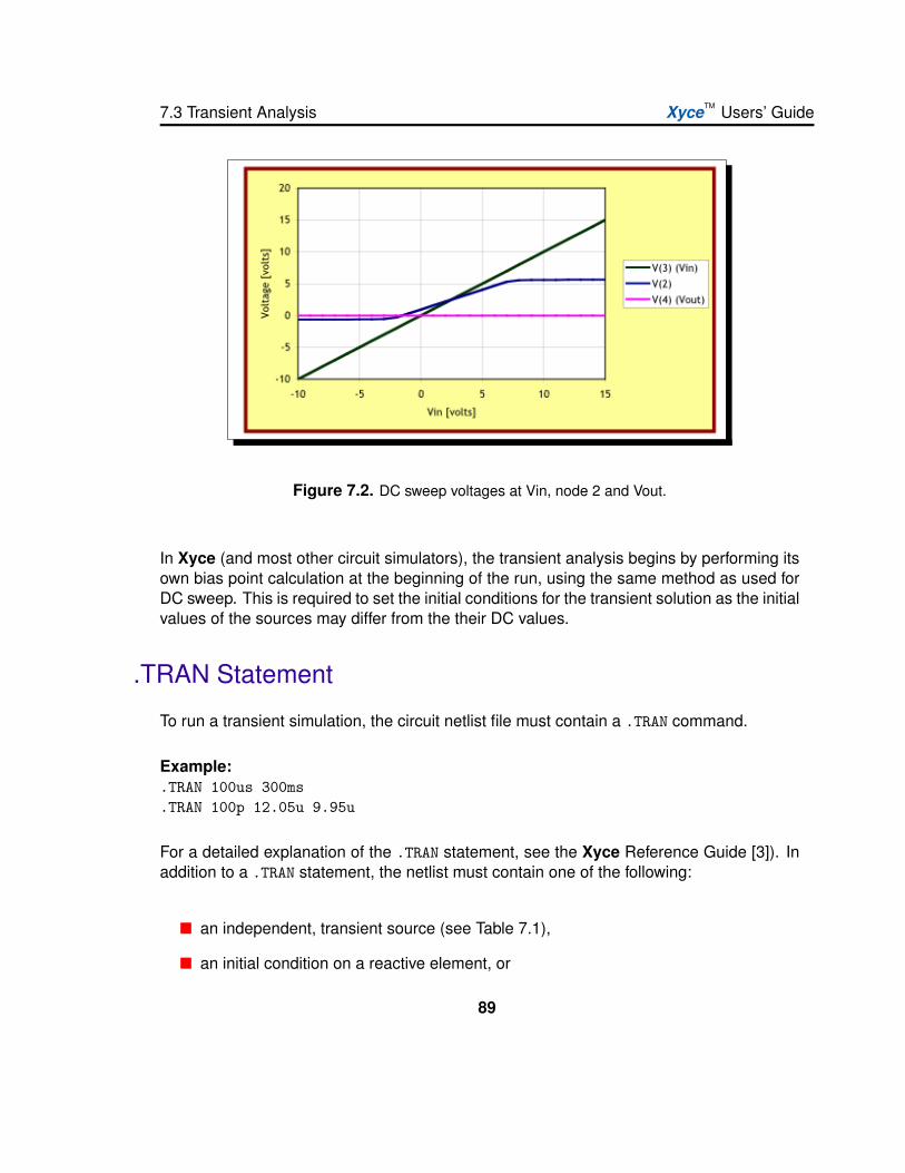
7.3 Transient Analysis XyceTM Users’ Guide
Figure 7.2. DC sweep voltages at Vin, node 2 and Vout.
In Xyce (and most other circuit simulators), the transient analysis begins by performing itsown bias point calculation at the beginning of the run, using the same method as used forDC sweep. This is required to set the initial conditions for the transient solution as the initialvalues of the sources may differ from the their DC values.
.TRAN Statement
To run a transient simulation, the circuit netlist file must contain a .TRAN command.
Example:.TRAN 100us 300ms.TRAN 100p 12.05u 9.95u
For a detailed explanation of the .TRAN statement, see the Xyce Reference Guide [3]). Inaddition to a .TRAN statement, the netlist must contain one of the following:
an independent, transient source (see Table 7.1),
an initial condition on a reactive element, or
89

XyceTM Users’ Guide Analysis Types
a time-dependent behavioral modeling source (see Chapter 6)
Defining a Time-Dependent (transient) Source
Overview of Source Elements
Source elements, either voltage or current, are entered in the netlist file as described in theXyce Reference Guide [3]. Table 7.1 list the time-dependent sources available in Xyce foreither voltage or current. For voltage sources, the name is preceded by the letter V whilecurrent sources are preceded by the letter I.
Source Element Name Description
EXP Exponential Waveform
PULSE Pulse Waveform
PWL Piecewise Linear Waveform
SFFM Frequency-modulated Waveform
SIN Sinusoidal Waveform
Table 7.1. Summary of time-dependent sources supported byXyce.
To use one of these time-dependent or transient sources, the user must place the sourceelement line in the netlist and characterize the transient behavior using the appropriateparameters. Each transient source element has a separate set of parameters dependenton its transient behavior. In this way, the user can create analog sources which producesine wave, square pulse, exponential pulse, single-frequency FM, and piecewise linearwaveforms.
Defining Transient Sources
To define a transient source:
Select one of the supported sources: independent voltage or current source.
Choose a transient source type from Table 7.1.
90

7.3 Transient Analysis XyceTM Users’ Guide
Provide the transient parameters (see the Xyce Reference Guide [3]) to fully definethe source.
Below is an example of an independent sinusoidal voltage source in a circuit netlist. Itcreates a voltage source between nodes 1 and 5 that oscillates sinusoidally between -5V and +5V with a frequency of 50 KHz. The arguments specify an offset of -5V, a 10Vamplitude, and a 50KHz frequency in that order.
Example: Vexample 1 5 SIN(-5V 10V 50K)
Transient Calculation Time Steps
During the simulation, Xyce uses a calculation time step that is continuously adjusted foraccuracy and efficiency (see [7] and [8]). During periods of circuit idleness the calculationtime step is increased, and during dynamic portions of the waveform it is decreased. Themaximum internal step size can be controlled by specifying the step ceiling value in the.TRAN command (see the Xyce Reference Guide [3]).
The internal calculation time steps used might not be consistent with the output time stepsrequested by the user. By default Xyce outputs solution results at every time step it cal-culates. If the user selects output timesteps via the .OPTIONS OUTPUT statement (seeChapter 9) then Xyce will output results at the interval requested, interpolating solutionvariables to desired output times if necessary.
Transient Time Step Selection Advice
There are two basic familes of step-size selection in Xyce. The first is Local TruncationError (LTE) based and the second is non-LTE based. There are two options that applyto both and they directly relate to how step-sizes are chosen right after breakpoints andbetween breakpoints. The option MINTIMESTEPSBP specifies the minimum number oftime-steps between breakpoints and effectively enforces a local maximum time-step. Theoption RESTARTSTEPSCALE determines the size of the first step coming out of a break-point. The step-size is calculated by multiplying RESTARTSTEPSCALE by the distancebetween the two breakpoints.
Example:.OPTIONS TIMEINT MINTIMESTEPSBP=100 RESTARTSTEPSCALE=0.001
91
XyceTM Users’ Guide Analysis Types
Local Trunction Error (LTE) Strategy
Both the BDF15 integrator and the Trapezoid integrator use the LTE based strategy bydefault. The strategy is to specify appropriate relative and absolute error tolerances. Theseare specified using .options timeint abstol=1.0e-6 reltol=1.0e-2. These are the defaultvalues.
Example:.OPTIONS TIMEINT ERROPTION=0 RELTOL=1e-1 ABSTOL=1e-5
One feature of the Trapezoid integrator is that there is no numerical dissipation introducedby the algorithm. This means that strong ringing will occur when discontinuities are intro-duced by sources or models. This ringing is entirely artificially introduced by the numericalalgorithm. This can result in a large local truncation error estimate ultimately leading to atime-step too small error. In this case, using a Non LTE strategy may help.
Non LTE Strategy
The Non LTE strategy used in Xyce is based on success of the nonlinear solve. Thisstrategy is enabled by setting ERROPTION=1. The behavior of this setting is slightly differ-ent for the BDF15 integrator and the Trapezoid integrator. Since the step-size selection isbased only upon nonlinear iteration statistics, and not accuracy, it is highly suggested thatDELMAX be specified in a circuit specific way.
For the BDF15 integrator, if the nonlinear solver converges then the step-size is doubled.On the other hand, if the nonlinear solver fails to converge, then the step-size is cut by oneeighth.
Example:.OPTIONS TIMEINT ERROPTION=1 DELMAX=1.0e-4
For the Trapezoid integrator, the options are slightly more refined. If the number of non-linear iterations is below NLMIN, then the step-size is doubled. If the number of nonlineariterations is above NLMAX then the step-size is cut by one eighth. In between, the step-size is left alone.
Example:
92

7.3 Transient Analysis XyceTM Users’ Guide
.OPTIONS TIMEINT METHOD=7 ERROPTION=1 NLMIN=3 NLMAX=8 DELMAX=1.0e-4
By default time-steps are not rejected unless the nonlinear solver fails to converge. Thisis the opposite of the default mode in LTE based step-selection. This can be enabled withTIMESTEPSREVERAL=1.
Example:.OPTIONS TIMEINT METHOD=7 ERROPTION=1 DELMAX=1.0e-4 TIMESTEPSREVERAL=1
Checkpointing and Restarting
The .OPTIONS RESTART command (in the netlist) is used to control all checkpoint outputand restarting. Checkpointing and associated restart can be extremely useful for longsimulations. In essence, Xyce allows the user to save the state of the simulation during arun (at intervals the user specifies) (checkpointing). This checkpoint data can then be readin to restart the simulation from any of the saved (checkpointed) time points.
Checkpointing Command Format
.OPTIONS RESTART PACK=<0|1> JOB=<job name> [INITIAL_INTERVAL=<interval>[<t0> <i0> [<t1> <i1>...]]]
PACK=<0|1> indicates whether the restart data files will contain byte packed data(1)or not(0). JOB=<job name> identifies the prefix for restart files. The actual restart fileswill be the job name appended with the current simulation time (e.g. name1e-05 forJOB=name and simulation time 1e-05 seconds). Furthermore, theINITIAL INTERVAL=<interval> identifies the initial interval time used for restart out-put. The <tx ix> intervals identify times (tx) at which the output interval (ix) willchange. This functionality is identical to that described for the .OPTIONS OUTPUTcommand (see Section 9.1).
Example - generate checkpoints at every time step (default):
.OPTIONS RESTART JOB=checkpt
Example - generate checkpoints every 0.1 µs:
.OPTIONS RESTART JOB=checkpt INITIAL_INTERVAL=0.1us
93
XyceTM Users’ Guide Analysis Types
Example - generate unpacked checkpoints every 0.1 µs:
.OPTIONS RESTART PACK=0 JOB=checkpt INITIAL_INTERVAL=0.1us
Example - Initial interval of 0.1 µs, at 1 µs in the simulation, change to interval of 0.5µs, and at 10 µs change to an interval of 0.1 µs:
.OPTIONS RESTART JOB=checkpt INITIAL_INTERVAL=0.1us 1us 0.5us+ 10us 0.1us
Restarting Command Format
.OPTIONS RESTART <FILE=<filename> | JOB=<job name> START_TIME=<time>>+ [INITIAL_INTERVAL=<interval> [<t0> <i0> [<t1> <i1> ...]]]
To restart from an existing restart file, the file can be specified by using either theFILE=<filename> parameter to explicitly request a file orJOB=<job name> START TIME=<time> to specify a file prefix and a specific time. The timemust exactly match an output file time for the simulator to correctly load the file. To continuegenerating restart output files, INITIAL INTERVAL=<interval> and following intervals canbe appended to the command in the same format as described above.
Example - Restart from checkpoint file at 0.133 µs:
.OPTIONS RESTART JOB=checkpt START_TIME=0.133us
Example - Restart from checkpoint file at 0.133 µs :
.OPTIONS RESTART FILE=checkpt0.000000133
Example - Restart from 0.133 µs and continue checkpointing at 0.1 µs intervals:
.OPTIONS RESTART FILE=checkpt0.000000133 JOB=checkpt_again+ INITIAL_INTERVAL=0.1us
94

7.4 STEP Parametric Analysis XyceTM Users’ Guide
7.4 STEP Parametric AnalysisThe .STEP command performs a parametric sweep for all the analyses of the circuit. Whenthis command is invoked, all of the typical analysis, such as .DC or .TRAN analysis areperformed at each parameter step.
This capability is very similar to the STEP capability in PSPICE [4], but not identical. In Xyce,.STEP can be used to sweep over any device instance or device model parameter, as wellas the circuit temperature. It is not legal to sweep parameters defined in .PARAM state-ments, but it is legal to sweep global parameters defined in .global param statements.See (Section 4.3) for a discussion of these two distinct parameter definitions.
.STEP Statement
One specifies a .STEP analysis by simply adding a .STEP line to a netlist. Note that unlike.DC, .STEP by itself is not an adequate analysis specification, as it merely specifies anouter loop around the normal analysis. There still needs to be a standard analysis line,either specifying .TRAN or .DC analysis.
Some examples of typical .STEP lines are:
Example:.STEP M1:L 7u 5u -1u.STEP OCT V0 0.125 64 2.STEP DEC R1 100 10000 3.STEP TEMP LIST 10.0 15.0 18.0 27.0 33.0
.STEP has a format similar to that of the .DC specification. In the first example, M1:L isthe name of the parameter, 7u is the initial value of the parameter, 5u is the final value ofthe parameter, and -1u is the step size. Like .DC, .STEP in Xyce can also handle sweepsby decade, octave or specified lists of values. For a complete explanation of each type ofsweep, consult the Xyce Reference Guide [3].
Sweeping over a Device Instance Parameter
The first example uses M1:L as the parameter, but it could have used any model or instanceparameter that existed in the circuit. Internally, Xyce handles the parameters for all device
95

XyceTM Users’ Guide Analysis Types
models and device instances in the same way. You can uniquely identify any parameterby specifying the device instance name, followed by a colon (:), followed by the specificparameter name. For example, all the MOSFET models have an instance parameter forthe channel length, L. If you have a MOSFET instance specified in a netlist, named M1,then the full name for M1’s channel length parameter is M1:L.
A simple application of .STEP to a device instance is given in figure 7.3. This is the samediode clipper circuit as was used in the transient analysis chapter, except that a single line(in red font) has been added. The .STEP line will cause Xyce to sweep the resistance ofthe resistor, R4, from 3.0 KOhms to 15.0 KOhms, in increments of 2.0 KOhms. This meansthat a total of seven transient simulations will be performed, each one with a different valuefor R4.
As the circuit is executed multiple times, the resulting output file is a little more sophisti-cated. The .PRINT statement is still used in much the same way as before. However, the.prn output file contains the concatenated output of each .STEP increment. For details ofhow .STEP changes output files, see the end of this section.
Sweeping over a Device Model Parameter
Sweeping a model parameter can be done in an identical manner to an instance parameter.Figure 7.4 contains the same circuit as in figure 7.3, but with a new .STEP line added. Thenew .STEP line refers to a model parameter, D1N3940:IS. Note that separate .STEP linesare the correct way to specify multiple parameters for a .STEP analysis. Each parameterneeds its own separate line. In this respect, the .STEP line syntax differs from the .DC linesyntax.
Sweeping over Temperature
It is also possible to sweep over temperature. To do so, simply specify temp as the param-eter name. It will work in the same manner as .STEP when applied to model and instanceparameters.
Special cases: Sweeping Independent Sources, Resistors,Capacitors
For some devices, there is generally only one parameter that one would want to actuallysweep. For example, a linear resistor’s only parameter of interest is the resistance, R. Sim-
96
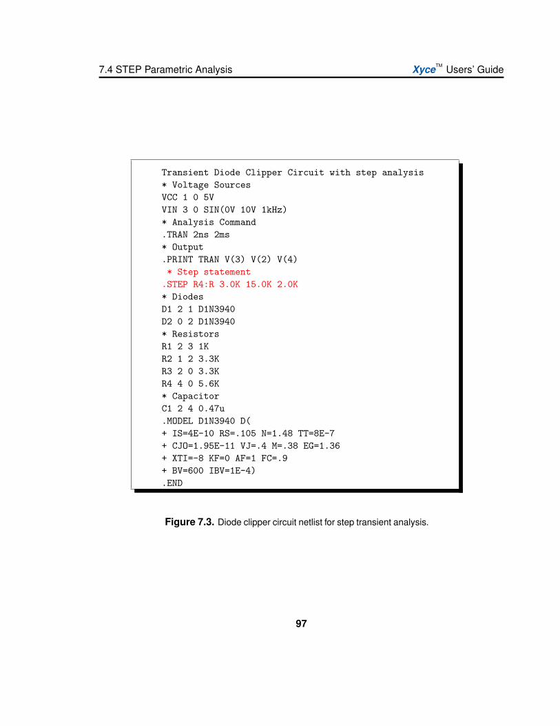
7.4 STEP Parametric Analysis XyceTM Users’ Guide
Transient Diode Clipper Circuit with step analysis* Voltage SourcesVCC 1 0 5VVIN 3 0 SIN(0V 10V 1kHz)* Analysis Command.TRAN 2ns 2ms* Output.PRINT TRAN V(3) V(2) V(4)* Step statement.STEP R4:R 3.0K 15.0K 2.0K* DiodesD1 2 1 D1N3940D2 0 2 D1N3940* ResistorsR1 2 3 1KR2 1 2 3.3KR3 2 0 3.3KR4 4 0 5.6K* CapacitorC1 2 4 0.47u.MODEL D1N3940 D(+ IS=4E-10 RS=.105 N=1.48 TT=8E-7+ CJO=1.95E-11 VJ=.4 M=.38 EG=1.36+ XTI=-8 KF=0 AF=1 FC=.9+ BV=600 IBV=1E-4).END
Figure 7.3. Diode clipper circuit netlist for step transient analysis.
97

XyceTM Users’ Guide Analysis Types
Transient Diode Clipper Circuit with step analysis* Voltage SourcesVCC 1 0 5VVIN 3 0 SIN(0V 10V 1kHz)* Analysis Command.TRAN 2ns 2ms* Output.PRINT TRAN V(3) V(2) V(4)* Step statements.STEP R4:R 3.0K 15.0K 2.0K.STEP D1N3940:IS 2.0e-10 6.0e-10 2.0e-10* DiodesD1 2 1 D1N3940D2 0 2 D1N3940* ResistorsR1 2 3 1KR2 1 2 3.3KR3 2 0 3.3KR4 4 0 5.6K* CapacitorC1 2 4 0.47u.MODEL D1N3940 D(+ IS=4E-10 RS=.105 N=1.48 TT=8E-7+ CJO=1.95E-11 VJ=.4 M=.38 EG=1.36+ XTI=-8 KF=0 AF=1 FC=.9+ BV=600 IBV=1E-4).END
Figure 7.4. Diode clipper circuit netlist for 2-step transient analy-sis.
98
7.4 STEP Parametric Analysis XyceTM Users’ Guide
ilarly, for a DC voltage or current source, one is usually only interested in the magnitude ofthe source. Finally, linear capacitors generally only have the capacitance, C, as a parame-ter of interest. To make things easier for the user, these three types of devices have defaultparameters. Examples of usage are given below.
Example:.STEP R4 3.0K 15.0K 2.0K.STEP VCC 4.0 6.0 1.0.STEP ICC 4.0 6.0 1.0.STEP C1 0.45u 0.50u 0.1u
Independent sources require some extra explanation. There are a number of differenttypes of independent sources, and only some of them have default parameters. Sourceswhich are subject to .DC sweeps (swept sources) do not have a default parameter, as thiscould easily lead to infinite loops. The various independent source defaults are defined intable 7.2.
Source Type Default
Sinusoidal source V0 (DC value, Offset)
Exponential source V1 (DC value, Initial value)
Pulsed source V2 (Pulsed value)
Constant, or DC source V0 (Constant value)
Piecewise Linear source No default
SFFM source No default
Swept source (specified on a .DC line) No default
Table 7.2: Default parameters for independent sources.
Output files
A .STEP simulation can be thought of as several distinct executions of the same circuitnetlist. The output data, as specified by a .PRINT line, however, goes to a single (*.prn)file. For convenience, a second auxilliary file is also created, with the *.res suffix.
The example file given in figure 7.3 has a filename of clip.cir. When run, it will producefiles clip.cir.res and clip.cir.prn. clip.cir.res contains one line for each step,showing what parameter value was used on that step. clip.cir.prn is the familiar output
99
XyceTM Users’ Guide Analysis Types
format, but the INDEX field recycles to zero each time a new step begins. Since the defaultbehavior distinguishes each step’s output only by recycling the INDEX field to zero, it canbe beneficial to add the sweep parameters to the .PRINT line. For the default file format(format=std), these sweep parameters will not be included automatically, so for plottingpurposes it is usually best to specify them by hand.
If using the default .prn file format (format=std), the output file resulting from a .STEPsimulation will be a simple concatenation of each step’s underlying analysis output. Ifusing format=probe, the data for each execution of the circuit will be in distinct sections ofthe file, and it should be easy to plot the results using PROBE. If using format=tecplot,the results of each .STEP simulation will be in a distinct tecplot zone.
100

7.5 Harmonic Balance Analysis XyceTM Users’ Guide
7.5 Harmonic Balance AnalysisHarmonic balance (HB) is a technique which solves for steady states of nonlinear circuitsin the frequency domain. It is well-suited for simulating RF and microwave circuits. Har-monic balance simulation solves for the magnitude and phase of voltages and currents ina nonlinear circuit.
Currently, Xyce supports single-tone HB for driven circuits in its serial build. Support formulti-tone HB and oscillator HB, as well as parallel HB, will come later.
.HB Statement
To run a HB simulation, the circuit netlist file must contain a .HB command.
Example:.HB 1e4
The parameter following .HB is the fundamental frequency. It must be specified by theuser. For a detailed explanation of the .HB statement, see the Xyce Reference Guide [3].
HB Options
Key parameters for HB simulation can be specified by .options hbint.
Example:.options hbint numfreq=41 STARTUPPERIODS=2
In the example above, numfreq specifies the number of harmonic frequencies to be calcu-lated and it must be an odd number. STARTUPPERIODS specifies the number of time periodsthat Xyce should integrate through using normal transient analysis before trying to gener-ate initial conditions for the HB analysis. For a detailed explanation of the HB options, seethe Xyce Reference Guide [3].
One of the most common errors in HB simulation setup is the use of too few harmonicfrequencies, i.e. numfreq is too small. You can determine what number of harmonic fre-quencies is optimum if you first simulate your circuit with a small numfreq then increase thenumfreq by 1 or 2 harmonics until the solution stops changing within a significant bound.
101
XyceTM Users’ Guide Analysis Types
Using too many harmonic frequencies is wasteful of memory, file size and simulation time,so it is not efficient to just clobber the problem with a very high numfreq.
HB Related Options
Nonlinear Solver Options
The HB analysis uses different set of default nonlinear solver parameters than that of tran-sient and DC analysis. Nonlinear solver parameters for HB simulation can be specified byusing .options nonlin-hb.
Example:.options nonlin-hb abstol=1e-6
For a detailed explanation of the .options nonlin-hb statement, see the Xyce ReferenceGuide [3].
Linear Solver Options
The single-tone HB analysis provided by Xyce employs direct solvers in the normal tran-sient analysis used to generate the initial conditions. However, during the HB analysis,only matrix-free operators are available, which require the use of iterative solvers. For amore detailed discussion of iterative solvers, see Section 10.4.
Preconditioners have been developed for the iterative solvers used in HB analysis. The it-erative solver and preconditioner options can be set using the .options hb-linsol state-ment.
Example:.options linsol-hb type=aztecoo prec type=block jacobi AZ tol=1e-9
In the example above, type specifies the iterative solver to use in the HB analysis andAZ tol is the relative tolerance for the iterative solver. Any of the iterative solver op-tions in Section 10.4 are valid options. However, prec type specifies which HB-specificpreconditioner to use and the choices for this option are none, which is the default, andblock jacobi.
102

7.6 Multi-Time PDE (MPDE) Analysis XyceTM Users’ Guide
7.6 Multi-Time PDE (MPDE) AnalysisXyce includes an analysis option specifically designed for circuits with two disparate timescales. For traditional transient analysis, a circuit with multiple time scales will requirethe time integrator to take many small time steps to adequately resolve the waveform.This can greatly slow simulation progress, and accuracy is reduced for long simulationsbecause error accumulates with each step.
For this type of system, Xyce can use an algorithm based on converting the originaldifferential-algebraic equation (DAE) to a multi-time partial differential equation(MPDE). [9]By doing so, problem is recast with two different time variables, representing a fast timescale and a slow one. The fast time scale is discretized and solved simultaneously at eachslow time scale step. If the two time scales are very different, one can dramatically reduceruntime, and also produce a more accurate simulation by using MPDE analysis,
How different the time scales must be is problem-dependent. The resolution of the fast timescale depends on the number fast time discretization points (set by the parameter N2), andthis number determines how different the time scales must be to justify using MPDE. If nfast time points are used, the MPDE problem size increases by a factor of n compared withtraditional transient simulation. This increases memory usage, and the cost of each timestep increases by a factor greater than n, as the linear solution time scales superlinearly.This additional expense is mitigated if the number of steps is decreased by substantiallymore than n. For example, a mixer circuit, in which two oscillatory inputs have frequenciesdiffering by 104, and which used n = 100 of would be a very good candidate circuit for thisalgorithm.
Note that circuits that do not have widely disparate timescales can often run successfullywith MPDE, in the sense that the algorithm will successfully converge, and run to comple-tion, but there is no benefit to doing so.
MPDE Usage
To use MPDE analysis in a simulation, place the following .mpde statement in the netlist:
Example:.mpde 0 1.0e-4
For a detailed explanation of the .mpde statement, see the Xyce Reference Guide [3].
103

XyceTM Users’ Guide Analysis Types
Key parameters for mpde simulation can be specified by .options mpdeint.
.OPTIONS MPDEINT OSCSRC=<v1,v2...> IC=<1,2> [optional switches]
OSCSRC=... A list of voltage or current sources that are to be considered as changingon the fast time scale. Typically these will be all the sources that change at or morequickly than the fast time scale.
IC=[1,2] Specifies the method used to calculate the initial conditions for the MPDEproblem. 1 uses the Sawtooth algorithm while 2 uses an initial transient run forthe initial condition. During the initial condition calculation, the slow sources aredeactivated so one is integrating only along the fast time axis.
N2=integer Specifies the number of equally spaced points to use in discretizing thefast time scale. This option can only be used exclusive of the AUTON2 and AUTON2MAXoptions.
AUTON2=[true | false] False by default. If it is set to true, then an initial transientrun is done to generate a mesh of time points for the fast time scale. The belief hereis that the time integrator can do a better job picking out where it needs more pointsto accurately describe the fast time solution. Note: you can use AUTON2 with IC=1 orIC=2. If you use it with IC=1, then the time mesh is just used for the set of points thefor the Sawtooth initial conditions. This option can only be used exclusive to the N2option.
AUTON2MAX=integer This sets the maximum number of fast time points that will bekept from the initial transient run so one has some control over the size of the simu-lation. If the initial transient run produces 2,000 points and this is set at 50, Xyce willuniformly sample points from the solution set for the MPDE simulation. This optioncan only be used exclusive to the N2 option.
STARTUPPERIODS=integer This is the number of fast time periods that Xyce shouldintegrate through using normal transient analysis before trying to generate initial con-ditions for the MPDE analysis.
diff=[0,1] Specifies the differentiation technique to use in calculating time deriva-tives on the fast time scale. 0 uses backward differences for the fast time differentia-tion while 1 uses central differences.
As an example here are two valid options lines for MPDE:
104

7.6 Multi-Time PDE (MPDE) Analysis XyceTM Users’ Guide
Example: .options MPDEINT IC=1 N2=21 OSCSRC=Vsine
Example: .options MPDEINT IC=2 AUTON2=true AUTON2MAX=50 OSCSRC=VIN1,VIN2
Driven Circuit Example: Gilbert Cell
An example MPDE netlist, for a driven circuit, is given in figure 7.7. Results for this circuitis given in figures 7.5 and 7.6. The circuit is a Gilbert cell mixer, and is a good candidatefor MPDE.
Figure 7.5. Gilbert Cell Result
105

XyceTM Users’ Guide Analysis Types
Figure 7.6. Gilbert Cell Result. This result is interpolated fromthe result in figure 7.5, from considering where t1=t2.
106
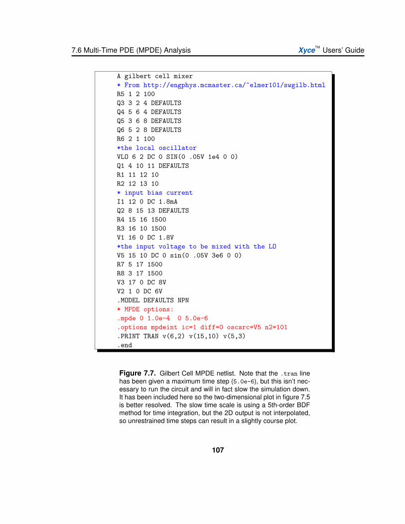
7.6 Multi-Time PDE (MPDE) Analysis XyceTM Users’ Guide
A gilbert cell mixer* From http://engphys.mcmaster.ca/~elmer101/swgilb.htmlR5 1 2 100Q3 3 2 4 DEFAULTSQ4 5 6 4 DEFAULTSQ5 3 6 8 DEFAULTSQ6 5 2 8 DEFAULTSR6 2 1 100*the local oscillatorVLO 6 2 DC 0 SIN(0 .05V 1e4 0 0)Q1 4 10 11 DEFAULTSR1 11 12 10R2 12 13 10* input bias currentI1 12 0 DC 1.8mAQ2 8 15 13 DEFAULTSR4 15 16 1500R3 16 10 1500V1 16 0 DC 1.8V*the input voltage to be mixed with the LOV5 15 10 DC 0 sin(0 .05V 3e6 0 0)R7 5 17 1500R8 3 17 1500V3 17 0 DC 8VV2 1 0 DC 6V.MODEL DEFAULTS NPN* MPDE options:.mpde 0 1.0e-4 0 5.0e-6.options mpdeint ic=1 diff=0 oscsrc=V5 n2=101.PRINT TRAN v(6,2) v(15,10) v(5,3).end
Figure 7.7. Gilbert Cell MPDE netlist. Note that the .tran linehas been given a maximum time step (5.0e-6), but this isn’t nec-essary to run the circuit and will in fact slow the simulation down.It has been included here so the two-dimensional plot in figure 7.5is better resolved. The slow time scale is using a 5th-order BDFmethod for time integration, but the 2D output is not interpolated,so unrestrained time steps can result in a slightly course plot.
107

XyceTM Users’ Guide
108
8. Using HomotopyAlgorithms to ObtainOperating Points
Chapter OverviewThis chapter includes the following sections:
Section 8.1, Homotopy Algorithms Overview
Section 8.2, MOSFET Homotopy
Section 8.3, Natural Parameter Homotopy
Section 8.4, Natural Multi-Parameter Homotopy
Section 8.5, GMIN Stepping Homotopy
Section 8.6, Pseudo Transient
109

XyceTM Users’ Guide Using Homotopy Algorithms to Obtain Operating Points
8.1 Homotopy Algorithms Overview
The most difficult type of circuit problem to solve can be the DC operating point. Unliketransient solves, DC operating point analysis cannot rely on a good initial guess from a pre-vious step, and also cannot simply reduce the step size when the solver fails. Additionally,operating points often have multiple solutions, sometimes intentional, and sometimes not.Multiple solutions can, even for circuit problems that converge, result in a standard Newtonsolve being unreliable. For example, it has been observed that the operating point solutionto a Schmidt trigger circuit may change from one hardware platform to another.
Homotopy methods can often provide solutions to difficult nonlinear problems, includingcircuit analysis, even when conventional methods (e.g. Newton’s method) fail [10] [11].This chapter gives an introduction to the usage of homotopy algorithms (sometimes calledcontinuation algorithms) in Xyce. For a more complete description of solver options, seethe Xyce Reference Guide [3].
HOMOTOPY Algorithms Available in Xyce
There are several types of homotopy which are available in Xyce. Most are accessible bysetting .options nonlin continuation=1, which allows the user to sweep existing deviceparameters (models and instances), as well as a few reserved artificial parameter cases.The most obvious natural parameter to use is the magnitude(s) of independent voltage orcurrent sources, the choice of which is equivalent to “source stepping” in SPICE. A Xycesource-stepping example is given in section 8.3. Note that for some circuits (like the aforementioned Schmidt trigger) source stepping will lead to turning points in the continuation.
“GMIN stepping”, another well-known SPICE method, is also invoked with .options nonlincontinuation=1 (and other parameters), and is a special case in that the parameter beingswept is artificial. An example of GMIN stepping is given in section 8.5.
A special Xyce-only homotopy is an algorithm which is designed specifically for MOSFETcircuits [12]. This algorithm involves two internal MOSFET model parameters, one for theMOSFET gain, and the other for the nonlinearity of the current-voltage relationship. Thisalgorithm is invoked with .options nonlin continuation=2. This algorithm has proved tobe very effective in some large MOSFET circuits. A detailed example is given in section 8.2.
110
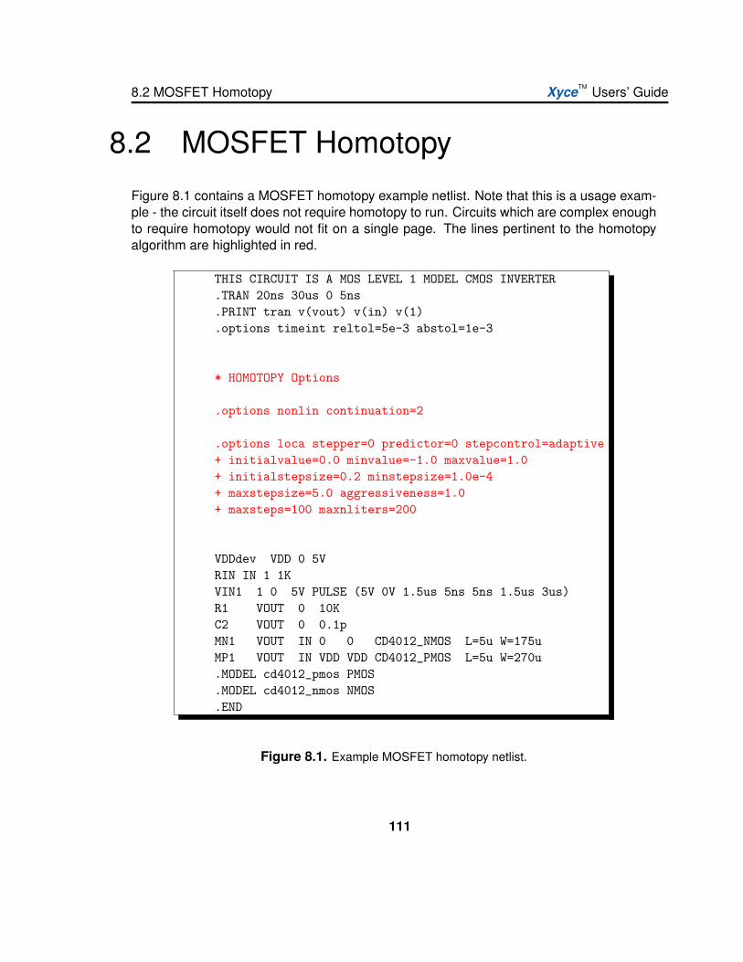
8.2 MOSFET Homotopy XyceTM Users’ Guide
8.2 MOSFET Homotopy
Figure 8.1 contains a MOSFET homotopy example netlist. Note that this is a usage exam-ple - the circuit itself does not require homotopy to run. Circuits which are complex enoughto require homotopy would not fit on a single page. The lines pertinent to the homotopyalgorithm are highlighted in red.
THIS CIRCUIT IS A MOS LEVEL 1 MODEL CMOS INVERTER.TRAN 20ns 30us 0 5ns.PRINT tran v(vout) v(in) v(1).options timeint reltol=5e-3 abstol=1e-3
* HOMOTOPY Options
.options nonlin continuation=2
.options loca stepper=0 predictor=0 stepcontrol=adaptive+ initialvalue=0.0 minvalue=-1.0 maxvalue=1.0+ initialstepsize=0.2 minstepsize=1.0e-4+ maxstepsize=5.0 aggressiveness=1.0+ maxsteps=100 maxnliters=200
VDDdev VDD 0 5VRIN IN 1 1KVIN1 1 0 5V PULSE (5V 0V 1.5us 5ns 5ns 1.5us 3us)R1 VOUT 0 10KC2 VOUT 0 0.1pMN1 VOUT IN 0 0 CD4012_NMOS L=5u W=175uMP1 VOUT IN VDD VDD CD4012_PMOS L=5u W=270u.MODEL cd4012_pmos PMOS.MODEL cd4012_nmos NMOS.END
Figure 8.1. Example MOSFET homotopy netlist.
111
XyceTM Users’ Guide Using Homotopy Algorithms to Obtain Operating Points
Explanation of Parameters, Best Practice
Note that this example shows one set of options, but there are a number of other combi-nations of options that will work.
There are a number of ”best practice” rules, which are illustrated by the example in fig-ure 8.1. They are:
continuation=2. This specifies that we are using the special MOSFET homotopy.This is a 2-pass homotopy, in which first a parameter having to do with the gain isswept from 0 to 1, and then a parameter relating to the nonlinearity of the transfercurve is swept from 0 to 1.
initialvalue=0.0. This is required.
maxvalue=1.0. This is required.
stepcontrol=1 or stepcontrol=adaptive. This specifies that the homotopy stepsare adaptive, rather than constant. This is recommended.
maxsteps=100. This sets the maximum number of continuation steps for each param-eter. For the special MOSFET continuation (which has 2 parameters), this means amaximum of 200 steps.
maxnliters=200. This is the maximum number of nonlinear iterations, and hasprecedence over the similar number which can be set on the .options nonlin line.
aggressiveness=1.0. This refers to the step size control algorithm, and the valueof this parameter can be anything from 0.0 to 1.0. 1.0 is the most aggressive. Inpractice, try starting with this set to 1.0. If the solver fails, then reset to a smallernumber.
8.3 Natural Parameter HomotopyFigure 8.2 contains a natural parameter homotopy netlist. It is the same circuit as wasused in figure 8.1, except that some of the parameters are different. As before, the linespertinent to the homotopy algorithm are highlighted in red.
112

8.3 Natural Parameter Homotopy XyceTM Users’ Guide
THIS CIRCUIT IS A MOS LEVEL 1 MODEL CMOS INVERTER.TRAN 20ns 30us 0 5ns.PRINT tran v(vout) v(in) v(1).options timeint reltol=5e-3 abstol=1e-3
* HOMOTOPY Options
.options nonlin continuation=1
.options loca stepper=0 predictor=0 stepcontrol=1+ conparam=VDDdev+ initialvalue=0.0 minvalue=-1.0 maxvalue=5.0+ initialstepsize=0.2 minstepsize=1.0e-4+ maxstepsize=5.0 aggressiveness=1.0+ maxsteps=100 maxnliters=200
VDDdev VDD 0 5VRIN IN 1 1KVIN1 1 0 5V PULSE (5V 0V 1.5us 5ns 5ns 1.5us 3us)R1 VOUT 0 10KC2 VOUT 0 0.1pMN1 VOUT IN 0 0 CD4012_NMOS L=5u W=175uMP1 VOUT IN VDD VDD CD4012_PMOS L=5u W=270u.MODEL cd4012_pmos PMOS.MODEL cd4012_nmos NMOS.END
Figure 8.2. Example natural parameter homotopy netlist.
113

XyceTM Users’ Guide Using Homotopy Algorithms to Obtain Operating Points
Explanation of Parameters, Best Practice
There are a few differences between the netlist in figure 8.1 and figure 8.2. They are:
continuation=1. Sets the algorithm to use natural parameter homotopy.
conparam=VDDdev. If using natural parameter homotopy, it is necessary include asetting for conparam. It sets which input parameter to perform continuation. Theparameter name is subject to the same rules as parameter used by the .STEP ca-pability. (See section 7.4). In this case the parameter is the magnitude of the DCvoltage source, VDDdev. For this type of voltage source, it was possible to use thedefault device parameter (see section 7.4)
Using the magnitudes of independent voltage and current sources is a fairly obvious ap-proach. Unfortunately, it doesn’t seem to work very well in practice.
8.4 Natural Multi-Parameter HomotopyIt is possible to use the natural parameter homotopy specification to have Xyce sweepmultiple parameters in sequential order. This requires that many of the parameters inthe .options loca statement be specified as vectors, delineated by commas, rather thanas single parameters. An example, which manually reproduces the MOSFET homotopyexample from figure 8.1, is given in figure 8.3.
Explanation of Parameters, Best Practice
The solver parameters set in figure 8.3 are the same as those from figure 8.1, but manyof them are in vector form. Any parameters that are specific to the continuation variablemust be specified as a vector. Parameter which are specified this way include conparam,initialvalue, minvalue, maxvalue, initialstepsize, minstepsize, maxstepsize, andaggressiveness. Otherwise, the specification is identical.
114

8.4 Natural Multi-Parameter Homotopy XyceTM Users’ Guide
THIS CIRCUIT IS A MOS LEVEL 1 MODEL CMOS INVERTER.TRAN 20ns 30us 0 5ns.PRINT tran v(vout) v(in) v(1).options timeint reltol=5e-3 abstol=1e-3
* HOMOTOPY Options
.options nonlin continuation=1
.options loca stepper=0 predictor=0 stepcontrol=adaptive+ conparam=mosfet:gainscale,mosfet:nltermscale+ initialvalue=0.0,0.0+ minvalue=-1.0,-1.0+ maxvalue=1.0,1.0+ initialstepsize=0.2,0.2+ minstepsize=1.0e-4,1.0e-4+ maxstepsize=5.0,5.0+ aggressiveness=1.0,1.0
VDDdev VDD 0 5VRIN IN 1 1KVIN1 1 0 5V PULSE (5V 0V 1.5us 5ns 5ns 1.5us 3us)R1 VOUT 0 10KC2 VOUT 0 0.1pMN1 VOUT IN 0 0 CD4012_NMOS L=5u W=175uMP1 VOUT IN VDD VDD CD4012_PMOS L=5u W=270u.MODEL cd4012_pmos PMOS.MODEL cd4012_nmos NMOS.END
Figure 8.3. Example multi-parameter homotopy netlist. Thisnetlist reproduces MOSFET homotopy with a manual specifica-tion.
115
XyceTM Users’ Guide Using Homotopy Algorithms to Obtain Operating Points
8.5 GMIN Stepping
A type of homotopy commonly available in circuit simulators is GMIN stepping. A netlistexample of GMIN stepping is shown in figure 8.4.
The name ”GMIN stepping” can be somewhat confusing, as ”GMIN” is also a user-specifieddevice package parameter that one can set, which is unrelated to this algorithm. In thiscontext, ”GMIN” refers to resistors attached from circuit nodes to ground. The GMIN step-ping algorithm involves attaching an artificial resistor to ground to every node in the circuit,with the intent of removing it later.
The continuation parameter is the conductance that is applied to the artificial resistors.Initially the conductance is very large, and is iteratively reduced until the artificial resistorshave a very high resistance. At the end of the continuation, the resistors are removed fromthe problem. At this point, assuming the continuation has been successful, the originaluser-specified problem has been solved.
Explanation of Parameters, Best Practice
In general, GMIN stepping can be very useful, but in most cases it should not be thefirst choice of algorithm for the operating point. For large MOSFET circuits, the MOSFET-homotopy (continuation=2) has been observed to be much more effective. For non-MOSFETcircuits, GMIN stepping may be a good candidate.
8.6 Pseudo Transient
Pseudo transient continuation is very similar to GMIN stepping, in that both algorithmsinvolve placing large artificial terms on the Jacobian matrix diagonal, and progressivelymaking these terms smaller until the original circuit problem is recovered. One difference isthat, rather than doing a series on Newton solves, Pseudo transient does a single nonlinearsolve while progressively modifying the pseudo transient parameter. An example of pseudotransient homotopy options is shown in figure 8.5.
116

8.6 Pseudo Transient XyceTM Users’ Guide
THIS CIRCUIT IS A GMIN STEPPING EXAMPLE..TRAN 20ns 30us 0 5ns.PRINT tran v(vout) v(in) v(1).options timeint reltol=5e-3 abstol=1e-3
* HOMOTOPY Options
.options nonlin continuation=1
.options loca+ stepper=natural+ predictor=constant+ stepcontrol=adaptive+ conparam=GSTEPPING+ initialvalue=4+ minvalue=-4+ maxvalue=4+ initialstepsize=-2+ minstepsize=1.0e-6+ maxstepsize=1.0e+12+ aggressiveness=0.01+ maxsteps=200+ maxnliters=20+ voltagelist=DOFS
VDDdev VDD 0 5VRIN IN 1 1KVIN1 1 0 5V PULSE (5V 0V 1.5us 5ns 5ns 1.5us 3us)R1 VOUT 0 10KC2 VOUT 0 0.1pMN1 VOUT IN 0 0 CD4012_NMOS L=5u W=175uMP1 VOUT IN VDD VDD CD4012_PMOS L=5u W=270u.MODEL cd4012_pmos PMOS.MODEL cd4012_nmos NMOS.END
Figure 8.4. Example GMIN stepping netlist. Note that the contin-uation type is 1, and the continuation parameter is called GSTEP-PING.
117
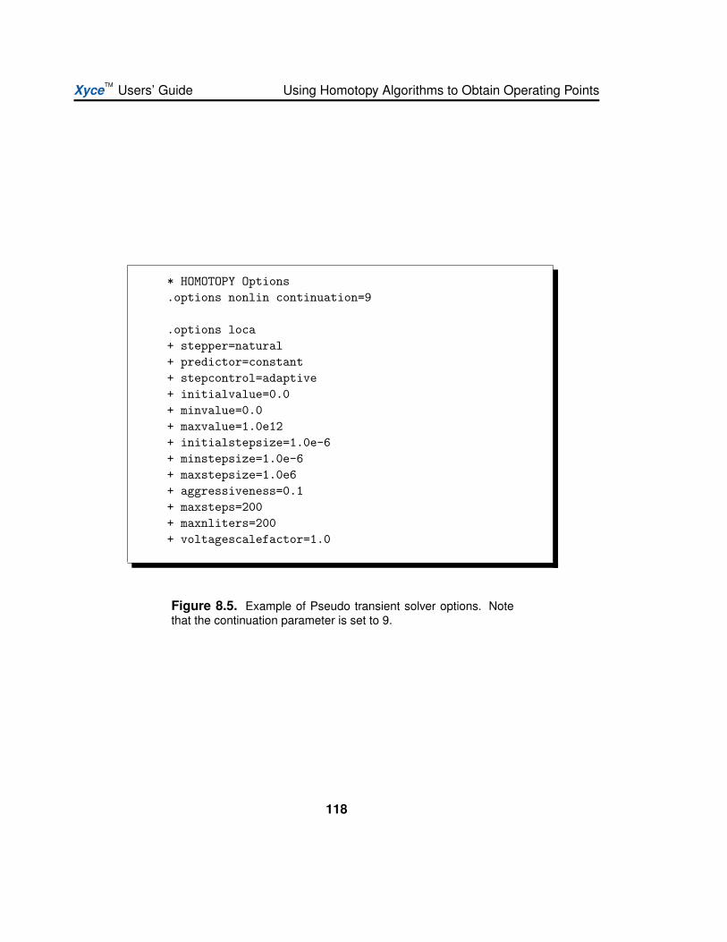
XyceTM Users’ Guide Using Homotopy Algorithms to Obtain Operating Points
* HOMOTOPY Options.options nonlin continuation=9
.options loca+ stepper=natural+ predictor=constant+ stepcontrol=adaptive+ initialvalue=0.0+ minvalue=0.0+ maxvalue=1.0e12+ initialstepsize=1.0e-6+ minstepsize=1.0e-6+ maxstepsize=1.0e6+ aggressiveness=0.1+ maxsteps=200+ maxnliters=200+ voltagescalefactor=1.0
Figure 8.5. Example of Pseudo transient solver options. Notethat the continuation parameter is set to 9.
118
8.6 Pseudo Transient XyceTM Users’ Guide
Explanation of Parameters, Best Practice
Similar to GMIN stepping, pseudo transient can be useful, but has not been observedto be as successful as MOSFET-homotopy for large MOSFET circuits. Similar to GMINStepping, for difficult non-MOSFET circuits it may be a good candidate. It will not workas often as GMIN stepping, but when it does work, it tends to be much faster, as the totalnumber of matrix solves is much smaller.
119

XyceTM Users’ Guide
120
9. Results Output andEvaluation Options
Chapter OverviewThis chapter illustrates how to output simulation results to data or output files.
Section 9.1, Control of Results Output
Section 9.2, Additional Output Options
Section 9.3, Graphical Display of Solution Results
121
XyceTM Users’ Guide Results Output and Evaluation Options
9.1 Control of Results OutputXyce supports only one solution output command, .PRINT. .PRINT is quite flexible, andsupports several output formats.
.PRINT Command
The .PRINT command sends the analysis results to an output file. Xyce supports severaloptions on the .PRINT line of netlists that control the format of the output. The syntax forthe command is as follows:
.PRINT <analysis type> [options] <output variable(s)>
Example:.PRINT TRAN FILE=Output.prn V(3) I(R3) ID(M5) V(4).PRINT DC format=tecplot FILE=Output.dat V(2) I(C3)+abs(V(4))*5.0
Table 9.1 gives the various options currently available to the .PRINT command. Note thatas of Xyce Release 3.0, it is possible to include device current or lead current specificationson the .PRINT line. Expressions can be output that include any valid .PRINT quantities. Forfurther information, see the Xyce Reference Guide [3].
9.2 Additional Output Options
.OPTIONS OUTPUT Command
The main purpose of the .OPTIONS OUTPUT command is to provide control of the frequencyat which data is written to files specified by .PRINT TRAN commands. This can be espe-cially useful in controlling the size of the results file for simulations which required a largenumber of time steps. An additional benefit is that reducing the output frequency from thedefault, which outputs results at every time-step, can improve performance. The format forcontrolling the output frequency is:
.OPTIONS OUTPUT INITIAL INTERVAL=<interval> [<t0> <i0> [<t1> <i1> ...]]
122
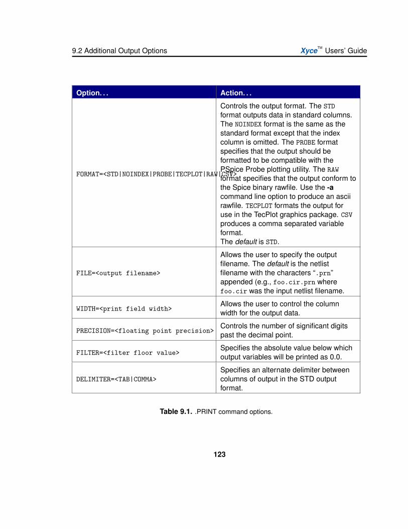
9.2 Additional Output Options XyceTM Users’ Guide
Option. . . Action. . .
FORMAT=<STD|NOINDEX|PROBE|TECPLOT|RAW|CSV>
Controls the output format. The STDformat outputs data in standard columns.The NOINDEX format is the same as thestandard format except that the indexcolumn is omitted. The PROBE formatspecifies that the output should beformatted to be compatible with thePSpice Probe plotting utility. The RAWformat specifies that the output conform tothe Spice binary rawfile. Use the -acommand line option to produce an asciirawfile. TECPLOT formats the output foruse in the TecPlot graphics package. CSVproduces a comma separated variableformat.The default is STD.
FILE=<output filename>
Allows the user to specify the outputfilename. The default is the netlistfilename with the characters “.prn”appended (e.g., foo.cir.prn wherefoo.cir was the input netlist filename.
WIDTH=<print field width>Allows the user to control the columnwidth for the output data.
PRECISION=<floating point precision>Controls the number of significant digitspast the decimal point.
FILTER=<filter floor value>Specifies the absolute value below whichoutput variables will be printed as 0.0.
DELIMITER=<TAB|COMMA>Specifies an alternate delimiter betweencolumns of output in the STD outputformat.
Table 9.1. .PRINT command options.
123

XyceTM Users’ Guide Results Output and Evaluation Options
where INITIAL_INTERVAL=<interval> specifies the starting interval time for output and<tx ix> specifies later simulation times (tx) where the output interval will change to (ix).
The following example shows the output being requested (via the netlist .OPTIONS OUTPUTcommand) every .1µs for the first 10µs, every 1µs for the next 10µs, and every 5µs for theremainder of the simulation:
Example: .OPTIONS OUTPUT INITIAL INTERVAL=.1us 10us 1us 20us 5us
9.3 Graphical Display of SolutionResults
Xyce does not provide integrated graphical display options, but it does produce output in aform that may readily be used with commonly available graphical tools. Popular choices ofgraphical viewers include TecPlot, gnuplot and MS Excel (see Figure 9.1 below for anexample plot using TecPlot, http://www.amtec.com). The standard Xyce print format(FORMAT=STD or FORMAT=NOINDEX) are well suited for use with gnuplot. Comma separatedvariable (FORMAT=CSV) is the best choice for import into Excel. FORMAT=TECPLOT producesoutput specifically targeted at the TecPlot tool. And by using the FORMAT=PROBE option tothe .PRINT command, Xyce is able to output .csd files which can be read by the PSpiceProbe utility to view the results. See the PSpice Users Guide [4] for instructions on usingthe Probe tool, and the Xyce Reference Guide [3] for details on the options to the .PRINTcommand.
124
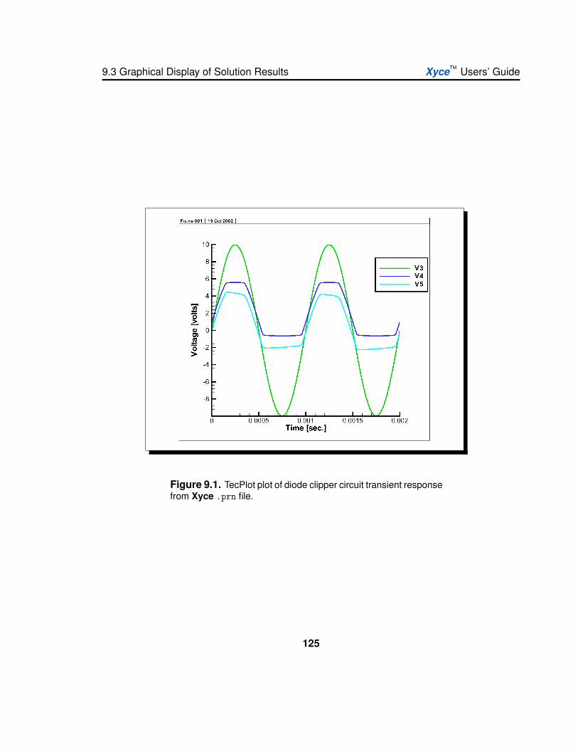
9.3 Graphical Display of Solution Results XyceTM Users’ Guide
Figure 9.1. TecPlot plot of diode clipper circuit transient responsefrom Xyce .prn file.
125

XyceTM Users’ Guide
126
10. Guidance forRunning Xyce in Parallel
Chapter OverviewThis chapter gives guidance on how to run a parallel version of Xyce. It includes thefollowing sections:
Section 10.1, Introduction
Section 10.2, Mechanics
Section 10.3, Problem Size
Section 10.4, Linear Solver Options
Section 10.5, Transformation Options
127
XyceTM Users’ Guide Guidance for Running Xyce in Parallel
10.1 IntroductionXyce has been designed, from the ground up, to support a message-passing parallel im-plementation. As such, Xyce is unique among circuit simulation tools, and many of theissues pertinent to running in parallel are still research issues. However, Xyce is nowmature enough that some general principles have emerged, for effectively running prob-lems in a parallel environment. In addition to the information in this chapter, supplementalinformation about Xyce parallel performance can be found in reference [13].
10.2 MechanicsParallel simulations must be run from the command line. Details of how to do this are givenin section 2.2.
10.3 Problem SizeDue to the overhead of interprocessor communication, running Xyce in parallel is onlyuseful for large circuit problems. Also, for any problem size, there is an optimal number ofprocessors. As one increases the processor count, the amount of communication requiredincreases and the work per processor decreases. This increase in communication will slowa simulation down, while the reduction in work per processor will have the reverse effect.If the number of processors is too large, the benefit of distributing the problem will beoutweighed by the high cost of communication overhead. Such a limit exists for every sizeof problem, and increasing the processor count beyond this point is counterproductive.This issue is most pronounced for platforms with a high communication cost, such asBeowulf clusters.
Smallest Possible Problem Size
Circuits are made up of a discrete set of components (voltage nodes, devices, etc.). To runin parallel, it is preferable that Xyce be able to put at least one discrete part of the problemon each processor. In practice, this means that the number of processors should be lessthan the number of nodes in the circuit. Xyce is capable of simulating smaller problems,but it is not recommended, due to solver instabilities.
128
10.4 Linear Solver Options XyceTM Users’ Guide
Ideal Problem Size
To take full advantage of Xyce’s parallel capability, the problem should be relatively large.A good metric for estimating how many processors one should use is the number of de-vices per processor. The ideal number of devices per processor is machine and problemdependent. For machines such as SGI Challenger platforms, with relatively fast commu-nication speeds in comparison to processor performance, reasonable speedups can beseen for 100’s of devices per processor. For Beowulf clusters with relatively slow commu-nication speeds in comparison to processor performance, 1000’s of devices per processorare required to achieve reasonable speedups in parallel. These numbers are problem-dependent, as the effectiveness of the load balance and partitioning can vary substantiallyfor different circuits.
10.4 Linear Solver Options
There are several different linear solvers available in Xyce version 5.2; they are:
The AztecOO iterative solver library.
KLU
SuperLU.
For Xyce version 5.2, AztecOO is the only fully parallel solver available. However, both KLUand SuperLU are available with the parallel version of Xyce. With the later two solvers, theproblem will be ”assembled” in parallel, but the linear system will be solved in serial onprocessor 0. This can be quite effective for smaller parallel problems of a few thousanddevices or less.
The solver can be specified through the .OPTIONS LINSOL control line in the netlist. Bydefault, the parallel version of Xyce uses AztecOO as the linear solver. Conversely, aserial version of Xyce uses KLU as its default linear solver. To use a solver other than thedefault the user needs to add the option “TYPE=<solver>” to the .OPTIONS LINSOL controlline in the netlist, where <solver> is ’KLU,’ ’SUPERLU’,’ or ’AZTECOO’.
129

XyceTM Users’ Guide Guidance for Running Xyce in Parallel
NOTE: An important caveat is that the performance and convergence of thelinear solver for parallel problems can be substantially less robust for somecircuits. This is a known issue with parallel iterative solution of linear prob-lems. If Xyce is not performing as expected for these problems, please con-sult the developer team.
AztecOO
AztecOO is a parallel, iterative, linear solver package in Trilinos. The iterative solver usedby Xyce is the Generalized Minimum Residual method, or GMRES. Some of the solverparameters for GMRES can be altered through the ’.OPTIONS LINSOL’ control line in thenetlist. These parameters can have a significant impact on performance of Xyce, so con-sult the developer team if you have any questions. Table 10.1 has a list of solver parametersfor AztecOO and their default values.
Option Description Default ValueAZ max iter Maximum allowed iterations 500AZ tol Iterative solver (relative residual) tolerance 1.0e-12AZ kspace Krylov subspace size 500OUTPUT LS Write out linear systems to file every # solves 0
Table 10.1. AztecOO linear solver options.
AztecOO Preconditioners
Iterative linear solvers often require the assistance of preconditioners to efficiently com-pute a solution of the linear system to the requested accuracy. In Xyce version 5.2, thepreconditioning interface has been expanded to allow the user to access multiple precon-ditioning packages in Trilinos, like Ifpack and ML. As of this release, user support is onlybeing offered for the Ifpack preconditioning options and the default behavior from previousreleases has been maintained.
If modifications to the preconditioner are necesary, the preconditioner can be specifiedthrough the ’.OPTIONS LINSOL’ control line in the netlist. Table 10.2 has a list of precondi-tioner parameters and their default values. These parameters can have a significant impacton performance of Xyce, so consult the developer team if you have any questions.
130
10.4 Linear Solver Options XyceTM Users’ Guide
Option Description Default Valueprec type Preconditioner IfpackAZ ilut fill ILU fill level 2.0AZ drop ILU drop tolerance 1.0e-3AZ overlap ILU subdomain overlap 0AZ athresh ILU absolute threshold 0.0001AZ rthresh ILU relative threshold 1.0001USE IFPACK FACTORY Additive Schwarz w/ KLU subdomain solve 0 (false)USE AZTEC PRECOND Use native ILU from AztecOO package 0 (false)
Table 10.2. AztecOO preconditioner options.
Common AztecOO Warnings
If Xyce is run with the verbosity enabled for the linear algebra package, it is not uncommonto see warnings from AztecOO. These warnings usually indicate that the solver returnedunconverged due to some numerical issue.
NOTE: Getting AztecOO warnings does not mean that the entire simulationhas failed. Xyce, like all circuit simulators, uses a hierarchy of solvers, andif the iterative linear solver fails, that often means that the nonlinear solver ortime integrator will then make adjustments and re-attempt the step. Gettingwarnings like the ones described here is usually not cause for concern, andthe warnings can often be ignored. If the entire simulation eventually doesfail (i.e. gets a ‘ ‘time-step-too-small” error), then the warnings from AztecOOmight contain clues as to what went wrong. However, by themselves they areusually benign.
The simplest reason for AztecOO to return unconverged would be when the maximumnumber of iterations was reached, which results in this warning:
***************************************************************Warning: maximum number of iterations exceeded without convergence***************************************************************
Another reason that AztecOO may return unconverged is when the GMRES Hessenbergmatrix is ill-conditioned. This is usually a sign that the matrix and/or preconditioner is nearly
131

XyceTM Users’ Guide Guidance for Running Xyce in Parallel
singular. The resulting warning looks like:
***************************************************************Warning: the GMRES Hessenberg matrix is ill-conditioned. This mayindicate that the application matrix is singular. In this case, GMRESmay have a least-squares solution.***************************************************************
It is also common to lose accuracy when the matrix and/or preconditioner are nearly sin-gular. GMRES relies on an estimate of the residual norm, called the recursive residual, todetermine convergence. The recursive residual is used instead of the actual residual forcomputational efficiency. However, numerical issues can cause the recursive residual todiffer from the actual residual. When that situation is detected by AztecOO, and cannot berectified, this warning will be outputted:
***************************************************************Warning: recursive residual indicates convergencethough the true residual is too large.
Sometimes this occurs when storage is overwritten (e.g. thesolution vector was not dimensioned large enough to holdexternal variables). Other times, this is due to roundoff. Inthis case, the solution has either converged to the accuracyof the machine or intermediate roundoff errors occurredpreventing full convergence. In the latter case, try solvingagain using the new solution as an initial guess.***************************************************************
KLU
KLU is a serial, sparse direct solver native to the Amesos package in Trilinos and is thedefault solver for serial versions of Xyce. KLU can be used in a parallel version of Xyceas well, but this requires the linear system to be solved on one processor and the solu-tion communicated back to all processors. As long as the linear system can fit on oneprocessor, KLU is often a superior approach to solving linear systems in parallel.
Some of the solver parameters for KLU can be altered through the ’.OPTIONS LINSOL’control line in the netlist. These parameters can have a significant impact on performance
132
10.5 Transformation Options XyceTM Users’ Guide
of Xyce, so consult the developer team if you have any questions. Table 10.3 has a list ofsolver parameters for KLU and their default values.
Option Description Default ValueKLU REPIVOT Recompute pivot order each solve 1 (true)OUTPUT LS Write out linear systems to file every # solves 0 (false)OUTPUT FAILED LS Write out failed linear systems to file 0 (false)
Table 10.3. KLU linear solver options.
SuperLU
SuperLU is a serial, sparse direct solver that has an interface in the Amesos package.Similar to KLU, SuperLU can be used in a parallel version of Xyce, but the linear systemis solved on one processor. Xyce does not allow any modification to SuperLU’s solverparameters at this time.
10.5 Transformation OptionsTransformations are often used to permute the original linear system to one that is easierfor direct or iterative linear solvers. Xyce currently has many different permutations thatcan by applied to remove dense rows and columns from a matrix, find a block triangularform, or partition the linear system for improved parallel performance.
Partitioning the Linear System
Partitioning subdivides the circuit problem into sections that are then distributed to theprocessors. A good partition can have a dramatic effect on the parallel performance ofcircuit simulation. There are two key components to a good partition:
Effective load balance.
Minimizing communication overhead.
133

XyceTM Users’ Guide Guidance for Running Xyce in Parallel
An effective load balance ensures that the computational load of the calculation is equallydistributed among the available processors. Minimizing communication overhead seeksto distribute the problem in a way that reduces the impact of underlying message passingduring the simulation run. For runs with a small number of devices per processor thecommunication overhead becomes the critical issue, while for runs with larger numbers ofdevices per processor the load balancing becomes more important.
Xyce currently has graph and hypergraph partitioning available. These partitioners areprovided via the Zoltan library of parallel partitioning heuristics that is integrated into Xyce.Access to Zoltan is provided via the Epetra Extended or Isorropia packages in Trilinos.
Zoltan can be controlled through the ’.OPTIONS LINSOL’ control line in the netlist. Table10.4 has the partitioning options and their default parameters. For parallel builds of Xyce,Zoltan is available and enabled by default to use the Isorropia interface and graph parti-tioning via ParMETIS. With Zoltan enabled, the linear system is statically load balanced,at the beginning of the simulation, based on the graph of the Jacobian matrix. The localsystem is also reordered based on nested dissection which should improve conditioningand minimize fill.
Option Description Default ValueTR PARTITION Partitioning package 0 (none), serial,
2 (Isorropia), parallelTR PARTITION TYPE Isorropia partitioner type GRAPH
Table 10.4. Partitioning options.
In Xyce version 5.2, the partitioning interface has been expanded to allow the user toaccess multiple partitioners through Isorropia. Changing the partitioner provided throughIsorropia is done by adding the ’TR PARTITION TYPE’ option to the ’.OPTIONS LINSOL’ con-trol line in the netlist. As of this release, there are two options for partitioning: graph(’TR PARTITION TYPE=GRAPH’) and hypergraph (’TR PARTITION TYPE=HYPERGRAPH’). Alter-natively, to access the deprecated interface to Zoltan’s graph partitioning through Epe-traExt, use ’TR PARTITION=1’ on the ’.OPTIONS LINSOL’ control line.
These techniques can be very effective for improving the efficiency of the iterative linearsolvers. See the Zoltan User Guide [14] for more details.
Occasionally it can be desirable to turn off the partitioning option, even for parallel simu-lations. To do so, the users should add the option ’.OPTIONS LINSOL TR PARTITION=0’ to
134
10.5 Transformation Options XyceTM Users’ Guide
disable Zoltan. In general, this is only recommended if the user wants to run a very smallcircuit in parallel.
Singleton Filtering of the Linear System
Singleton filtering is a transformation that reduces the linear system through removal of allrows and columns with single non-zero entries. The values associated with these removedentries can be resolved as pre/post linear solve operations. A by-product of this transfor-mation is a more tractable and sparse linear system for both the load balancing and linearsolver algorithms. This functionality is turned on by adding the ’TR SINGLETON FILTER=1’option to the ’.OPTIONS LINSOL’ control line in the netlist.
AMD Ordering of the Linear System
Approximate Minimum Degree (AMD) ordering is a symmetric permutation that reducesthe fill-in for a Cholesky factoriztion. If given a nonsymmetric matrix A, the transformationcomputes the AMD ordering of A + AT . For parallel builds of Xyce, AMD ordering is en-abled by default. Otherwise, the AMD transformation is turned on by adding the ’TR AMD=1’option to the ’.OPTIONS LINSOL’ control line in the netlist.
Permuting the Linear System to Block Triangular Form
The block triangular form (BTF) permutation is often useful for direct or iterative solvers,enabling a more efficient computation of the linear system solution. In particular, the BTFpermutation has shown promise when it is combined with an incomplete factorization pre-conditioner, such as ILU, in the simulation of circuits with unidirectional flow.
In Xyce version 5.2, a new transformation is being offered to complement the new precondi-tioner interface, ’TR GLOBAL BTF’. The global BTF transformation computes the permutationof the linear system to BTF form, as well as partitions the linear system. The partitioningcan be a simple linear distribution of block rows, ’TR GLOBAL BTF=1’, or a hypergraph par-titioning of block rows, ’TR GLOBAL BTF=2’. Since the global BTF transformation includeselements of other tranformations, it is imperative that some other linear solver options beset. To use the global BTF, the linear solver control line in the netlist should at least contain:
.OPTIONS LINSOL TR_GLOBAL_BTF=<1,2> TR_SINGLETON_FILTER=1+ TR_AMD=0 TR_PARTITION=0
135

XyceTM Users’ Guide Guidance for Running Xyce in Parallel
These parameters can have a significant impact on performance of Xyce, so consult thedeveloper team if you have any questions.
136
11. Handling Power NodeParasitics
Chapter OverviewThis chapter includes the following sections:
Section 11.1, Power Node Parasitics
Section 11.2, Two Level Algorithms Overview
Section 11.3, Examples
Section 11.4, Restart
137
XyceTM Users’ Guide Handling Power Node Parasitics
11.1 Power Node Parasitics
Parasitic elements (R, L, C) are frequently required for circuit simulations to capture impor-tant circuit behavior. Most parasitic elements (interconnect, etc.) can be added to netlistswithout causing any difficulties for the Xyce solvers. Small circuits in particular are veryrobust to the addition of parasitic elements. Larger circuits, however, that must be sim-ulated in parallel will in general tend to have more solver difficulties with the addition ofparasitic devices. Of particular note are parasitic elements attached to the power and/orground nodes of large digital circuits. As these nodes tend to be highly connected, theycan potentially have very high impact on solver difficulties.
One of the parallel algorithms used by Xyce is called singleton removal. This algorithmis applied at the linear solver level and is crucial for getting many large circuits to run inparallel. This algorithm takes advantage of the fact that, in circuit simulation, some solutionvalues are available explicitly, rather than being a quantity that needs to be calculated asthe solution to a particular equation. In circuit simulation, such quantities are usually thevalues of independent sources. For instance, the presence of an independent voltagesource at a particular node in a circuit fixes the voltage at that node to be the value ofthe independent source; therefore, equations reflecting the value of the voltage at thatparticular node do not have to be added to the set of linear equations that are used (inpart) to determine the voltages at all nodes in the circuit. The technique of fixing suchnode voltages without including them in the rest of the linear solve can be handled in apreprocessing phase referred to as the singleton removal phase.
When simulating in parallel, singleton removal is crucial since some voltage sources (espe-cially power supplies in digital circuits) are connected to hundreds or thousands of circuitnodes. In parallel, this presents a big problem because a large number of connectionscan often mean a communication bottleneck during the linear solve. The use of singletonremoval eliminates that bottleneck.
While singleton removal can result in a great improvement for circuits with ideal powersupplies, for circuits with non-ideal power supplies, the communication bottleneck remains.Once parasitic elements are placed between the power supply and the rest of the circuit, itis only the voltage at the circuit node which is directly connected to the independent sourcethat can be removed via singleton removal. All of the other nodes that are connected tothis independent source through parasitic elements have voltages that must now be solvedfor directly.
138
11.2 Two Level Algorithms Overview XyceTM Users’ Guide
11.2 Two Level Algorithms OverviewFortunately there is a workaround in Xyce which allows power node parasitics to be in-cluded in large circuits without breaking singleton removal. The workaround requires theuse of a two-level Newton solve, in which the problem is broken up into two very separatepieces. Each piece is, for the most part, treated as an entirely separate circuit with minimalcoupling terms linking the pieces together.
For power-node problems, two-level users will typically split the netlist into ”top” and ”inner”netlists. The top netlist should contain the power node parasitics and the ideal voltagesources, and very little else. The inner circuit should contain the rest of the circuit. The twocircuits are coupled through a ”EXT” (external) device in the top circuit, and two or moreindependent voltage sources on the inner circuit. The values on the inner voltages areimposed from the top circuit, and the currents and conductances of the EXT device comefrom the inner circuit.
Xyce will treat the two circuits separately, constructing a different linear system for eachone. As such, the inner circuit will appear to have independent sources, and the singletonremoval algorithm will still work.
The two-level Newton algorithm has been in the literature since (at least) the 1980’s, al-though in the past it has mostly been applied to circuit-device simulation. For a mathemat-ical description, see [15] and [16].
11.3 Examples
Explanation and Guidance
An example of a circuit that uses the two level algorithm is given in figures 11.1 and 11.2.The top circuit (compTop.cir) is given in the first figure, and this top circuit invokes theinner circuit (compInner.cir) with the extern device, y1. To run this circuit, the user will onlyspecify the top circuit on the command line:
Xyce compTop.cir <return>
The extern device (YEXT y1 sits between the contents of compTop.cir and compInner.cir.It is connected to two nodes in the top level circuit, DD1 and SS1. From the perspective of
139
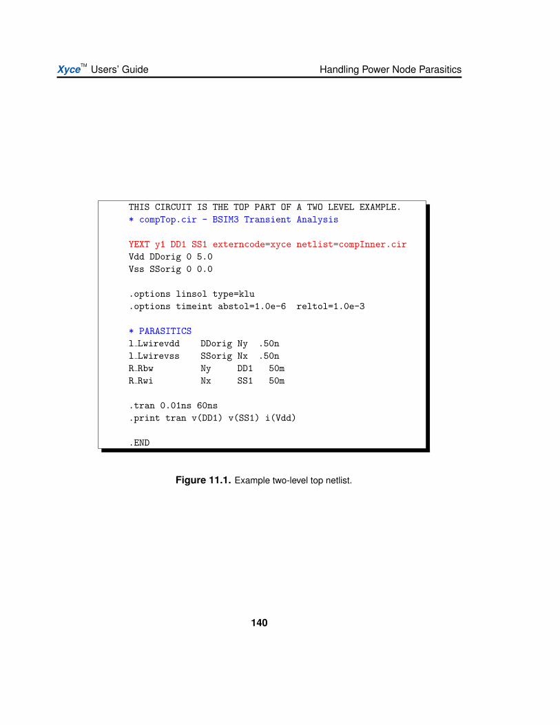
XyceTM Users’ Guide Handling Power Node Parasitics
THIS CIRCUIT IS THE TOP PART OF A TWO LEVEL EXAMPLE.* compTop.cir - BSIM3 Transient Analysis
YEXT y1 DD1 SS1 externcode=xyce netlist=compInner.cirVdd DDorig 0 5.0Vss SSorig 0 0.0
.options linsol type=klu
.options timeint abstol=1.0e-6 reltol=1.0e-3
* PARASITICSl Lwirevdd DDorig Ny .50nl Lwirevss SSorig Nx .50nR Rbw Ny DD1 50mR Rwi Nx SS1 50m
.tran 0.01ns 60ns
.print tran v(DD1) v(SS1) i(Vdd)
.END
Figure 11.1. Example two-level top netlist.
140

11.3 Examples XyceTM Users’ Guide
THIS CIRCUIT IS THE INNER PART OF A TWO LEVEL EXAMPLE.* compInner.cir - BSIM3 Transient AnalysisM1 Anot A DD1 DD1 PMOS w=3.6u l=1.2uM2 Anot A SS1 SS1 NMOS w=1.8u l=1.2uM3 Bnot B DD1 DD1 PMOS w=3.6u l=1.2uM4 Bnot B SS1 SS1 NMOS w=1.8u l=1.2uM5 AorBnot SS1 DD1 DD1 PMOS w=1.8u l=3.6uM6 AorBnot B 1 SS1 NMOS w=1.8u l=1.2uM7 1 Anot SS1 SS1 NMOS w=1.8u l=1.2uM8 Lnot SS1 DD1 DD1 PMOS w=1.8u l=3.6uM9 Lnot Bnot 2 SS1 NMOS w=1.8u l=1.2uM10 2 A SS1 SS1 NMOS w=1.8u l=1.2uM11 Qnot SS1 DD1 DD1 PMOS w=3.6u l=3.6uM12 Qnot AorBnot 3 SS1 NMOS w=1.8u l=1.2uM13 3 Lnot SS1 SS1 NMOS w=1.8u l=1.2uMQLO 8 Qnot DD1 DD1 PMOS w=3.6u l=1.2uMQL1 8 Qnot SS1 SS1 NMOS w=1.8u l=1.2uMLTO 9 Lnot DD1 DD1 PMOS w=3.6u l=1.2uMLT1 9 Lnot SS1 SS1 NMOS w=1.8u l=1.2uCQ Qnot 0 30fCL Lnot 0 10f
Vconnect0000 DD1 0 0Vconnect0001 SS1 0 0
Va A 0 pulse(0 5 10ns .1ns .1ns 15ns 30ns)Vb B 0 0
.model nmos nmos (level=9)
.model pmos pmos (level=9)
.options linsol type=klu
.options timeint abstol=1.0e-6 reltol=1.0e-3
.tran 0.01ns 60ns
.print tran v(a) v(b) 1.0+v(9) 1.0+v(8)
.END
Figure 11.2. Example two-level inner netlist.
141

XyceTM Users’ Guide Handling Power Node Parasitics
compTop.cir, the YEXT y1 device just looks like a nonlinear two-terminal resistor, which isthe equivalent of the entire inner circuit.
In the inner circuit, the nodes DD1 and SS1 are applied though the independent sourcesVconnect0000 and Vconnect0001. By convention, the inner circuit must contain and inde-pendent voltage source for each node to which the EXT device is connected. The defaultnaming convention requires that these sources be named vconnectxxxx, with xxxx beinga four digit integer starting at 0000.
Note that the .tran statement on the inner circuit must match the .tran statement on thetop circuit. The same is true for .DC analysis.
Note also that both circuit files have their own .print statements. That means that theywill both produce *.prn output files.
The coupling between the top and inner layers requires extra linear solves, so when usingthis algorithm the code will run more slowly. In general, one can usually expect a factor oftwo slowdown, for circuits that can be run either as conventional or two-level simulations.So, in practice this algorithm should only be applied when it is really needed (i.e., whenconventional simulations fail).
Finally, when using this method, one must take particular care with file names. In practice,a Xyce user may frequently change netlist file names to reflect new details about the run.When this happens, the name of the netlist invoked on the YEXT y1 line must be changed.Failure to do so may result in using the wrong file for the inner simulation.
11.4 RestartRestart works with the two-level algorithm. However, as the two-level algorithm involvestwo separate netlist input files, two-level restart requires a separate restart file for eachphase of the problem. So, the two files (for example compTop.cir and compInner.cir) needto have .options restart statements, and the statements in the two files need to beconsistent with each other.
Currently, the code does not make any attempt to check if the ”.options restart” statementin the top file is consistent with the ”.options restart” statement in the inner file. It is up tothe user to enforce this.
142

12. Specifying InitialConditions
Chapter OverviewThis chapter includes the following sections:
Section 12.1, Initial Conditions Overview
Section 12.2, Device Level IC= Specification
Section 12.3, .IC and .DCVOLT Initial Condition Statements
Section 12.4, .NODESET Initial Condition Statements
Section 12.5, .SAVE Statements
Section 12.6, DCOP Restart
Section 12.7, UIC and NOOP
143
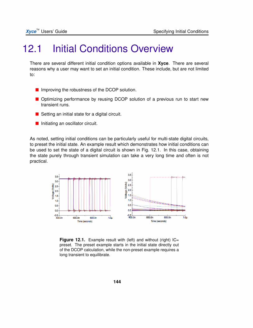
XyceTM Users’ Guide Specifying Initial Conditions
12.1 Initial Conditions OverviewThere are several different initial condition options available in Xyce. There are severalreasons why a user may want to set an initial condition. These include, but are not limitedto:
Improving the robustness of the DCOP solution.
Optimizing performance by reusing DCOP solution of a previous run to start newtransient runs.
Setting an initial state for a digital circuit.
Initiating an oscillator circuit.
As noted, setting initial conditions can be particularly useful for multi-state digital circuits,to preset the initial state. An example result which demonstrates how initial conditions canbe used to set the state of a digital circuit is shown in Fig. 12.1. In this case, obtainingthe state purely through transient simulation can take a very long time and often is notpractical.
Figure 12.1. Example result with (left) and without (right) IC=preset. The preset example starts in the initial state directly outof the DCOP calculation, while the non-preset example requires along transient to equilibrate.
144

12.2 Device Level IC= Specification XyceTM Users’ Guide
12.2 Device Level IC= SpecificationMany devices in Xyce support setting initial junction voltage conditions on the device in-stance line with the IC= keyword. This has frequently been used to set the state of digitalcircuits. A very simple inverter example that demonstrates usage of IC= on a BSIMSOIdevice is shown in Fig. 12.2.
While many circuit simulators have a similar IC= capability, the Xyce implementation differsin some important respects. For any device that has an IC= statement, Xyce enforcesthe junction drop in parallel with the device junction as a voltage source in parallel withthe device. This parallel voltage source is applied through the DCOP calculation, and isthen removed prior to the beginning of the transient. This strongly enforces the requestedjunction drop, meaning that if the DCOP converges, the requested voltage drop will in thesolution. In many other circuit codes, IC= is applied as a weaker constraint, with the intentof improving DCOP calculation robustness.
Currently, IC= can be applied to the following devices: BSIM3, BSIM4, BSIMSOI, Capacitorand Inductor. This capability may be added to other devices in the future, depending onuser requests.
145
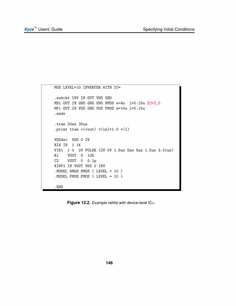
XyceTM Users’ Guide Specifying Initial Conditions
MOS LEVEL=10 INVERTER WITH IC=
.subckt INV IN OUT VDD GNDMN1 OUT IN GND GND GND NMOS w=4u l=0.15u IC=2,0MP1 OUT IN VDD GND VDD PMOS w=10u l=0.15u.ends
.tran 20ns 30us
.print tran v(vout) v(in)+1.0 v(1)
VDDdev VDD 0 2VRIN IN 1 1KVIN1 1 0 2V PULSE (2V 0V 1.5us 5ns 5ns 1.5us 3.01us)R1 VOUT 0 10KC2 VOUT 0 0.1pXINV1 IN VOUT VDD 0 INV.MODEL NMOS NMOS ( LEVEL = 10 ).MODEL PMOS PMOS ( LEVEL = 10 )
.END
Figure 12.2. Example netlist with device-level IC=.
146
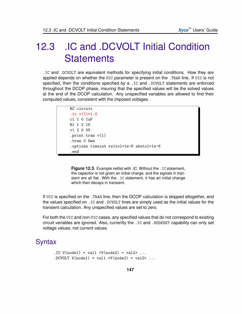
12.3 .IC and .DCVOLT Initial Condition Statements XyceTM Users’ Guide
12.3 .IC and .DCVOLT Initial ConditionStatements
.IC and .DCVOLT are equivalent methods for specifying initial conditions. How they areapplied depends on whether the UIC parameter is present on the .TRAN line. If UIC is notspecified, then the conditions specified by a .IC and .DCVOLT statements are enforcedthroughout the DCOP phase, insuring that the specified values will be the solved valuesat the end of the DCOP calculation. Any unspecified variables are allowed to find theircomputed values, consistent with the imposed voltages.
RC circuit.ic v(1)=1.0c1 1 0 1uFR1 1 2 1Kv1 2 0 0V.print tran v(1).tran 0 5ms.options timeint reltol=1e-6 abstol=1e-6.end
Figure 12.3. Example netlist with .IC. Without the .IC statement,the capacitor is not given an initial charge, and the signals in tran-sient are all flat. With the .IC statement, it has an initial changewhich then decays in transient.
If UIC is specified on the .TRAN line, then the DCOP calculation is skipped altogether, andthe values specified on .IC and .DCVOLT lines are simply used as the initial values for thetransient calculation. Any unspecified values are set to zero.
For both the UIC and non-UIC cases, any specified values that do not correspond to existingcircuit variables are ignored. Also, currently the .IC and .NODESET capability can only setvoltage values, not current values.
Syntax.IC V(node1) = val1 <V(node2) = val2> ....DCVOLT V(node1) = val1 <V(node2) = val2> ...
147

XyceTM Users’ Guide Specifying Initial Conditions
where: val1, val2, ... specify nodal voltages and node1, node2, ... specify node numbers.
Example.IC V(1) = 2.0 V(A) = 4.5.DCVOLT 1 2.0 A 4.5
A more complete example (showing a full netlist) is given in Fig. 12.3.
148
12.4 .NODESET Initial Condition Statements XyceTM Users’ Guide
12.4 .NODESET Initial ConditionStatements
.NODESET is similar to .IC, except that Xyce enforces the specified conditions less strongly.For .NODESET simulations, Xyce does two nonlinear solves for the DCOP condition. Forthe first solve, the .NODESET values are enforced throughout the solve, similar to .IC. Forthe second solve, the result of the first solve is used as an initial guess, and all the valuesare allowed to float and eventually obtain their unconstrained, self-consistent values. Assuch, the computed values will not necessarily match the specified values. .NODESET isgenerally used to help with difficult nonlinear solves, but should only be used if the userwants a fully self-consistent initial DCOP computation. For an inconsistent initial condition,one should use .IC instead.
.NODESET V(node1) = val1 <V(node2) = val2> ...
.NODESET node1 val1 <node2 val2>
where: val1, val2, ... specify nodal voltages and node1, node2, ... specify node numbers.
Example.NODESET V(1) = 2.0 V(A) = 4.5.NODESET 1 2.0 A 4.5
149

XyceTM Users’ Guide Specifying Initial Conditions
12.5 .SAVE StatementsOperating point information can be stored using the .SAVE statements, and then reused tostart subsequent transient simulations. Using .SAVE will result in solution data being storedin a text file, comprised of .NODESET or .IC statements. This file can be applied to othersimulations using .INCLUDE.
The form of .SAVE is as follows:
.SAVE <TYPE=type keyword> <FILE=save file> <LEVEL=level keyword> <TIME=save time>
where:
type keyword can be set to “NODESET” or “IC”. By default, it will be “IC”.
save file is the user specified output file name for the *.ic file. If this is not specified, Xycewill use netlist.cir.ic.
level keyword is an Hspice compatibility parameter. Currently, Xyce only supports “ALL”and ”NONE”.
save time is an Hspice compatibility parameter. Currently it is unsupported, and Xyce canonly output the *.ic file at time=0.0.
150
12.6 DCOP Restart XyceTM Users’ Guide
12.6 DCOP RestartDCOP restart is a capability that is very similar to .NODESET and .SAVE used in combination.Similar to .NODESET, starting a simulation with DCOP restart will result in Xyce performingtwo nonlinear solves. The first solve strictly enforces the previous answer, and the secondsolve allows all the values to float and obtain their unconstrained solution. The secondsolve relies on the results of the first solve as an initial guess.
If the UIC keyword appears on the .TRAN line, then the contents of the DCOP restart filewill be applied as the initial condition and the DCOP calculation will be skipped altogether.This is, of course, the same as for .IC and .NODESET.
While .NODESET and DCOP restart are very similar, there are a few differences. Thebiggest difference is the handling of voltage source voltages and currents. DCOP restartwill attempt to restart from all the variables of the simulation, including voltage source vari-ables. .NODESET, on the other hand, will ignore specified variables associated with voltagesources, and explicitly does not allow currents to be set. In general, voltage sources areconstraints in and of themselves, so re-constraining them can cause singular matrices. Toavoid this issue, DCOP restart, makes changes to the linear system to prevent matricesfrom being singular.
Saving a DCOP restart file
To create a DCOP restart file, a .DCOP output=filename line needs to be added to thenetlist:
.dcop output=saved.op
This will result in the file “saved.op” being produced immediately after the operating pointcalculation. The produced file is similar to a *.ic file that can be produced by .SAVE, butwith different format. Similar to the the *.ic file, it is a text file, and has two columns. Onecolumn has the variable name, the other column the value of that variable.
Loading a DCOP restart file
To use a DCOP restart file, a .DCOP input=filename line needs to be added to the netlist:
151

XyceTM Users’ Guide Specifying Initial Conditions
.dcop input=saved.op
If the specified file does not exist in the local directory, then Xyce will simply ignore the.DCOP statement and run normally.
152
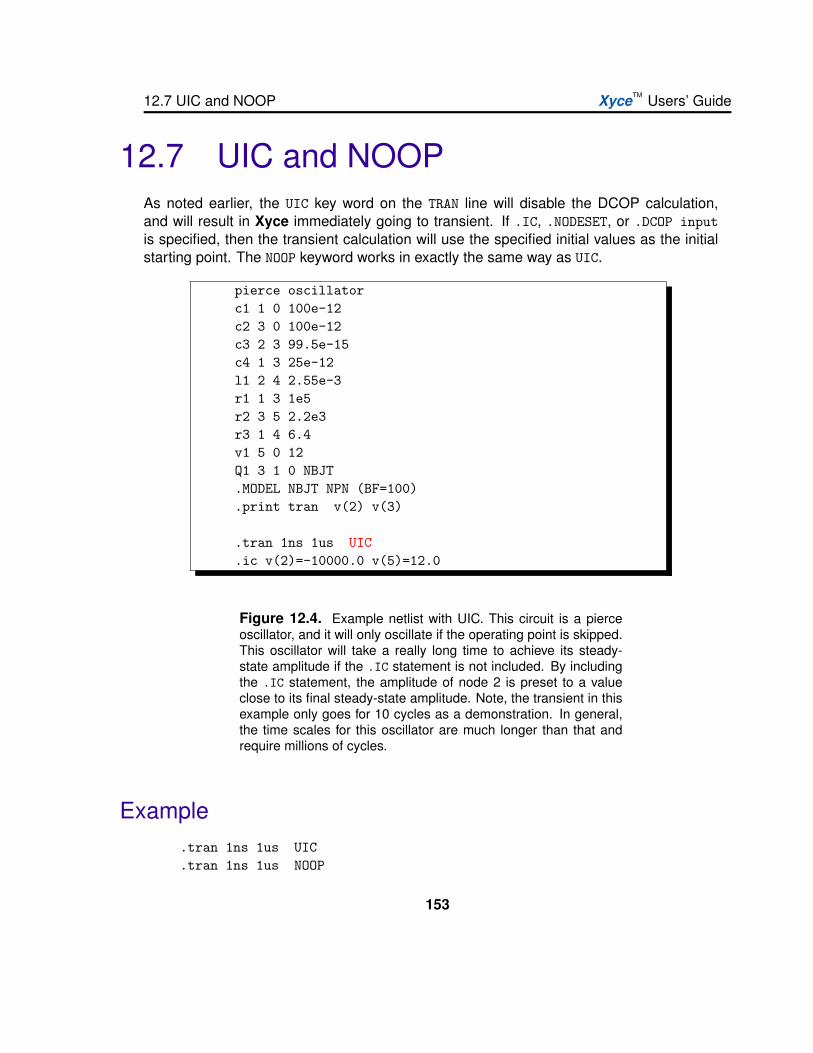
12.7 UIC and NOOP XyceTM Users’ Guide
12.7 UIC and NOOPAs noted earlier, the UIC key word on the TRAN line will disable the DCOP calculation,and will result in Xyce immediately going to transient. If .IC, .NODESET, or .DCOP inputis specified, then the transient calculation will use the specified initial values as the initialstarting point. The NOOP keyword works in exactly the same way as UIC.
pierce oscillatorc1 1 0 100e-12c2 3 0 100e-12c3 2 3 99.5e-15c4 1 3 25e-12l1 2 4 2.55e-3r1 1 3 1e5r2 3 5 2.2e3r3 1 4 6.4v1 5 0 12Q1 3 1 0 NBJT.MODEL NBJT NPN (BF=100).print tran v(2) v(3)
.tran 1ns 1us UIC
.ic v(2)=-10000.0 v(5)=12.0
Figure 12.4. Example netlist with UIC. This circuit is a pierceoscillator, and it will only oscillate if the operating point is skipped.This oscillator will take a really long time to achieve its steady-state amplitude if the .IC statement is not included. By includingthe .IC statement, the amplitude of node 2 is preset to a valueclose to its final steady-state amplitude. Note, the transient in thisexample only goes for 10 cycles as a demonstration. In general,the time scales for this oscillator are much longer than that andrequire millions of cycles.
Example.tran 1ns 1us UIC.tran 1ns 1us NOOP
153

XyceTM Users’ Guide Specifying Initial Conditions
Some circuits, particularly oscillator circuits, will only function properly if the operating pointis skipped, as they need an inconsistent initial state to oscillate. A pierce oscillator exampleis given in Fig. 12.4.
154
13. Working with.PREPROCESSCommands
Chapter OverviewThis chapter includes the following sections:
Section 13.1, Introduction
Section 13.2, Ground Synonym Replacement
Section 13.3, Removal of Unused Components
Section 13.4, Adding Resistors to Dangling Nodes
155
XyceTM Users’ Guide Working with .PREPROCESS Commands
13.1 IntroductionIn an effort to make Xyce more compatible with other commercial circuit simulators (e.g.,HSPICE), some optional tools have been added to increase Xyce’s netlist processing ca-pabilities. These options, which occur toward the beginning of a simulation, have beenincorporated not only to make Xyce more compatible with different (i.e. non-Xyce) netlistsyntax, but also to help detect and remove certain singular netlist configurations that canoften cause a Xyce simulation to fail. Because all of the commands we describe belowoccur as a precursory step to setting up a Xyce simulation, they are all invoked in a netlistfile via the keyword .PREPROCESS. In this chapter, we describe each of the different func-tionalities that can be invoked via a .PREPROCESS statement in detail and provide examplesto illustrate its use.
13.2 Ground Synonym ReplacementIn certain versions of Spice, keywords such as GROUND, GND, and GND! can be used asnode names in a netlist file to represent the ground node of a circuit. Xyce, however, onlyrecognizes node 0 as an official name for ground. Hence, if any of the prior node namesis encountered in a netlist file, Xyce will treat these as different nodes from ground. Toillustrate this point, consider the netlist of Fig. 13.1. When the node Gnd is encountered inthe definition of resistor R3, Xyce instantitates this as a new node. The schematic diagramcorresponding to this netlist (depicted in Fig. 13.2) shows that the resistor R3 is “floating”between node 2 and a node which has only a single device connection, node Gnd. Whenthe netlist of Fig. 13.1 is executed in Xyce, the voltage V(2) will evaluate to 0.5V.
If it is the case that one wishes for Gnd to be treated the same as node 0 in the above exam-ple, one can use the netlist of Fig. 13.3 instead. The statement .PREPROCESS REPLACEGROUNDTRUE has the following effect: if this statement is present in a netlist, Xyce will treat anynodes named GND, GND!, GROUND, or any capital/lowercase variant of these keywords (e.g.,gROunD) as synonyms for node 0. Hence, according to Xyce, the netlist of Fig. 13.3 corre-sponds to the schematic diagram of Fig. 13.4, and the voltage V(2) will evaluate to 0.33V.
A few comments are in order. First, only one .PREPROCESS REPLACEGROUND statement isallowed per netlist file (this is to prevent the user from setting REPLACEGROUND to TRUE onone line and then to FALSE on another). Secondly, there is currently no way to differentiatebetween different keywords, i.e., it is not possible to treat GROUND as a synonym for node0 while allowing GND to represent an independent node. If REPLACEGROUND is set to TRUE,both of these keywords will be treated as node 0 if present in a netlist file.
156
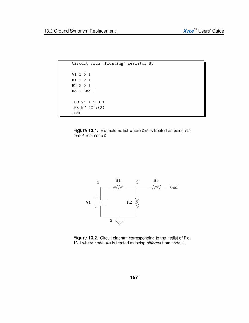
13.2 Ground Synonym Replacement XyceTM Users’ Guide
Circuit with "floating" resistor R3
V1 1 0 1R1 1 2 1R2 2 0 1R3 2 Gnd 1
.DC V1 1 1 0.1
.PRINT DC V(2)
.END
Figure 13.1. Example netlist where Gnd is treated as being dif-ferent from node 0.
.........................................................................................................................................................
....................................
......................................
......................................
......................................
.......................................
......................................
......................................
......................................
...
R1
R2V1
1 2Gnd
0
R3
-
+
............................................
........
Figure 13.2. Circuit diagram corresponding to the netlist of Fig.13.1 where node Gnd is treated as being different from node 0.
157

XyceTM Users’ Guide Working with .PREPROCESS Commands
Circuit where resistor R3 does *not* float
V1 1 0 1R1 1 2 1R2 2 0 1R3 2 Gnd 1
.PREPROCESS REPLACEGROUND TRUE
.DC V1 1 1 0.1
.PRINT DC V(2)
.END
Figure 13.3. Example netlist where Gnd is treated as a synonymfor node 0.
....................................
......................................
......................................
......................................
...
.........................................................................................................................................................
.........................................................................................................................................................
R1
R2 R3V1
1 2
0
-
+
............................................
........
Figure 13.4. Circuit diagram corresponding to Fig. 13.3 wherenode Gnd is treated as a synonym for node 0.
158
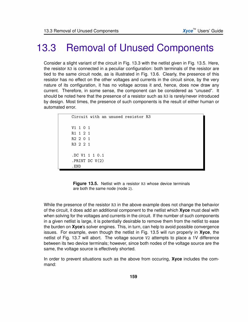
13.3 Removal of Unused Components XyceTM Users’ Guide
13.3 Removal of Unused ComponentsConsider a slight variant of the circuit in Fig. 13.3 with the netlist given in Fig. 13.5. Here,the resistor R3 is connected in a peculiar configuration: both terminals of the resistor aretied to the same circuit node, as is illustrated in Fig. 13.6. Clearly, the presence of thisresistor has no effect on the other voltages and currents in the circuit since, by the verynature of its configuration, it has no voltage across it and, hence, does now draw anycurrent. Therefore, in some sense, the component can be considered as “unused”. Itshould be noted here that the presence of a resistor such as R3 is rarely/never introducedby design. Most times, the presence of such components is the result of either human orautomated error.
Circuit with an unused resistor R3
V1 1 0 1R1 1 2 1R2 2 0 1R3 2 2 1
.DC V1 1 1 0.1
.PRINT DC V(2)
.END
Figure 13.5. Netlist with a resistor R3 whose device terminalsare both the same node (node 2).
While the presence of the resistor R3 in the above example does not change the behaviorof the circuit, it does add an additional component to the netlist which Xyce must deal withwhen solving for the voltages and currents in the circuit. If the number of such componentsin a given netlist is large, it is potentially desirable to remove them from the netlist to easethe burden on Xyce’s solver engines. This, in turn, can help to avoid possible convergenceissues. For example, even though the netlist in Fig. 13.5 will run properly in Xyce, thenetlist of Fig. 13.7 will abort. The voltage source V2 attempts to place a 1V differencebetween its two device terminals; however, since both nodes of the voltage source are thesame, the voltage source is effectively shorted.
In order to prevent situations such as the above from occuring, Xyce includes the com-mand:
159
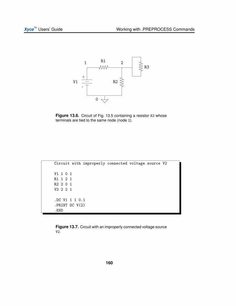
XyceTM Users’ Guide Working with .PREPROCESS Commands
.........................................................................................................................................................
....................................
......................................
......................................
......................................
...
....................
........................................
........................................
........................................
.............R1
R2V1
1 2
0
R3
-
+
............................................
........
Figure 13.6. Circuit of Fig. 13.5 containing a resistor R3 whoseterminals are tied to the same node (node 2).
Circuit with improperly connected voltage source V2
V1 1 0 1R1 1 2 1R2 2 0 1V2 2 2 1
.DC V1 1 1 0.1
.PRINT DC V(2)
.END
Figure 13.7. Circuit with an improperly connected voltage sourceV2.
160
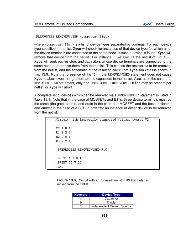
13.3 Removal of Unused Components XyceTM Users’ Guide
.PREPROCESS REMOVEUNUSED <component list>
where <component list> is a list of device types separated by commas. For each devicetype specified in the list, Xyce will check for instances of that device type for which all ofthe device terminals are connected to the same node. If such a device is found, Xyce willremove that device from the netlist. For instance, if we execute the netlist of Fig. 13.8,Xyce will seek out resistors and capacitors whose device terminals are connected to thesame node and remove them from the netlist. This causes the resistor R3 to be removedfrom the netlist, and the schematic of the resulting circuit that Xyce simulates is shown inFig. 13.9. Note that presence of the “C” in the REMOVEUNUSED statement does not causeXyce to abort even though there are no capacitors in the netlist. Also, as in the case of aREPLACEGROUND statement, only one .PREPROCESS REMOVEUNUSED line may be present pernetlist, or Xyce will abort.
A complete list of devices which can be removed via a REMOVEUNUSED statement is listed inTable 13.1. Note that in the case of MOSFETs and BJTs, three device terminals must bethe same (the gate, source, and drain in the case of a MOSFET and the base, collector,and emitter in the case of a BJT) in order for an instance of either device to be removedfrom the netlist.
Circuit with improperly connected voltage source V2
V1 1 0 1R1 1 2 1R2 2 0 1R3 2 2 1
.PREPROCESS REMOVEUNUSED R,C
.DC V1 1 1 0.1
.PRINT DC V(2)
.END
Figure 13.8. Circuit with an “unused” resistor R3 that gets re-moved from the netlist.
Keyword Device TypeC CapacitorD DiodeI Independent Current Source
161

XyceTM Users’ Guide Working with .PREPROCESS Commands
Keyword Device TypeL InductorM MOSFETQ BJTR ResistorV Independent Voltage Source
Table 13.1: List of keywords and device types which can be usedin a .PREPROCESS REMOVEUNUSED statement.
13.4 Adding Resistors to DanglingNodes
Consider the netlist of Fig. 13.10 and the corresponding schematic of Fig. 13.11. Nodes3 and 4 of the netlist are what we will henceforth refer to as dangling nodes. We saythat node 4 dangles because it is only connected to the terminal of a single device, whilewe say that node 3 dangles because it has no DC path to ground. The first of thesesituations—connection to a single device terminal only—can arise, for example, in a netlistwhich contains nodes representing output pins that are not connected to a load device. Forinstance, the resistance R2 in Fig. 13.10 could represent the resistance of an output pin of apackage that is meant to drive resistive loads. Hence, an actual physical implementation ofthe circuit of Fig. 13.11 would normally include a resistor between node 4 and ground, but,in creating the netlist, the presence of such an output load has been (either intentionally orunintentionally) left out.
The second situation—where a node has no DC path to ground—is sometimes an ef-fect that is purposely incorporated into a design (e.g., the design of switched capacitorintegrators—see, e.g., Chapter 10 of [17]), but it is also oftentimes the result of some formof error in the process of creating the netlist. For instance, when graphical user inter-faces (GUIs) are used to create circuit schematics which are then translated into netlistsvia software, one very common unintentional error is to fail to connect two nodes whichare intended to be connected. To illustrate this point, consider the schematic of Fig. 13.12.The schematic seems to indicate that the lower terminal of resistor R2 should be connectedto node 3, but this is in fact not the case since there is a small gap between node 3 andthe line which is intended to connect node 3 to the resistor. Such an error can often gounnoticed when creating a schematic of the netlist in a GUI. Thus, when the schematic istranslated into a netlist file, the resulting netlist would not connect the resistor to node 3and would instead create a new node at the bottom of the resistor, resulting in the circuit
162
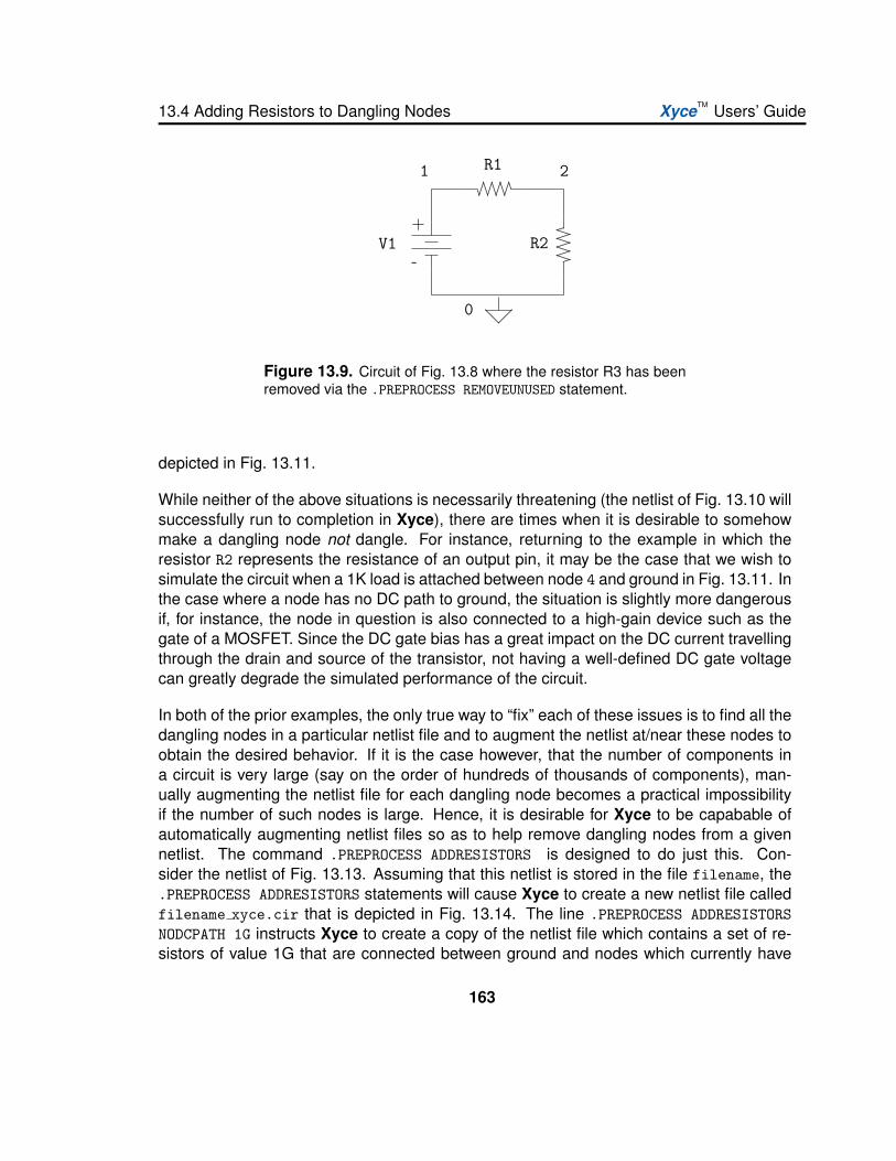
13.4 Adding Resistors to Dangling Nodes XyceTM Users’ Guide
.........................................................................................................................................................
....................................
......................................
......................................
......................................
...
R1
R2V1
1 2
0
-
+
............................................
........
Figure 13.9. Circuit of Fig. 13.8 where the resistor R3 has beenremoved via the .PREPROCESS REMOVEUNUSED statement.
depicted in Fig. 13.11.
While neither of the above situations is necessarily threatening (the netlist of Fig. 13.10 willsuccessfully run to completion in Xyce), there are times when it is desirable to somehowmake a dangling node not dangle. For instance, returning to the example in which theresistor R2 represents the resistance of an output pin, it may be the case that we wish tosimulate the circuit when a 1K load is attached between node 4 and ground in Fig. 13.11. Inthe case where a node has no DC path to ground, the situation is slightly more dangerousif, for instance, the node in question is also connected to a high-gain device such as thegate of a MOSFET. Since the DC gate bias has a great impact on the DC current travellingthrough the drain and source of the transistor, not having a well-defined DC gate voltagecan greatly degrade the simulated performance of the circuit.
In both of the prior examples, the only true way to “fix” each of these issues is to find all thedangling nodes in a particular netlist file and to augment the netlist at/near these nodes toobtain the desired behavior. If it is the case however, that the number of components ina circuit is very large (say on the order of hundreds of thousands of components), man-ually augmenting the netlist file for each dangling node becomes a practical impossibilityif the number of such nodes is large. Hence, it is desirable for Xyce to be capabable ofautomatically augmenting netlist files so as to help remove dangling nodes from a givennetlist. The command .PREPROCESS ADDRESISTORS is designed to do just this. Con-sider the netlist of Fig. 13.13. Assuming that this netlist is stored in the file filename, the.PREPROCESS ADDRESISTORS statements will cause Xyce to create a new netlist file calledfilename xyce.cir that is depicted in Fig. 13.14. The line .PREPROCESS ADDRESISTORSNODCPATH 1G instructs Xyce to create a copy of the netlist file which contains a set of re-sistors of value 1G that are connected between ground and nodes which currently have
163
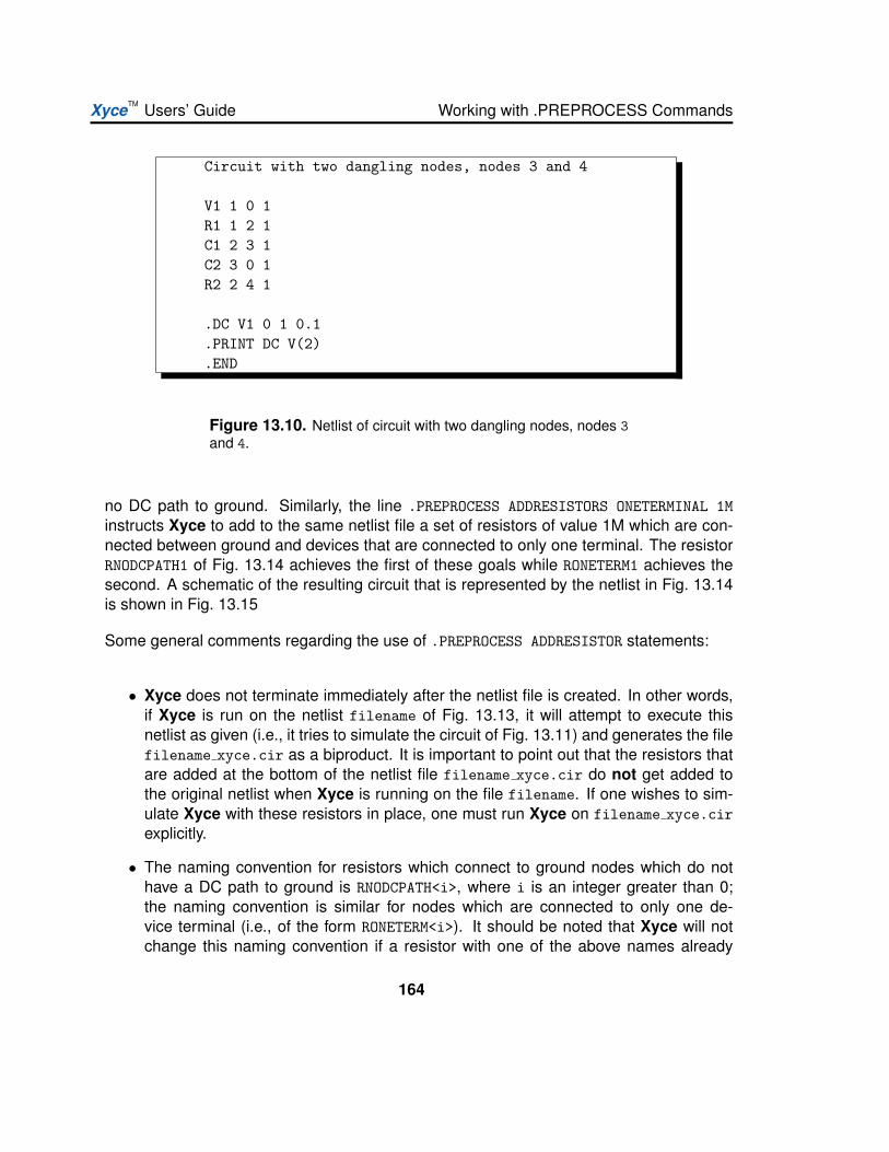
XyceTM Users’ Guide Working with .PREPROCESS Commands
Circuit with two dangling nodes, nodes 3 and 4
V1 1 0 1R1 1 2 1C1 2 3 1C2 3 0 1R2 2 4 1
.DC V1 0 1 0.1
.PRINT DC V(2)
.END
Figure 13.10. Netlist of circuit with two dangling nodes, nodes 3and 4.
no DC path to ground. Similarly, the line .PREPROCESS ADDRESISTORS ONETERMINAL 1Minstructs Xyce to add to the same netlist file a set of resistors of value 1M which are con-nected between ground and devices that are connected to only one terminal. The resistorRNODCPATH1 of Fig. 13.14 achieves the first of these goals while RONETERM1 achieves thesecond. A schematic of the resulting circuit that is represented by the netlist in Fig. 13.14is shown in Fig. 13.15
Some general comments regarding the use of .PREPROCESS ADDRESISTOR statements:
• Xyce does not terminate immediately after the netlist file is created. In other words,if Xyce is run on the netlist filename of Fig. 13.13, it will attempt to execute thisnetlist as given (i.e., it tries to simulate the circuit of Fig. 13.11) and generates the filefilename xyce.cir as a biproduct. It is important to point out that the resistors thatare added at the bottom of the netlist file filename xyce.cir do not get added tothe original netlist when Xyce is running on the file filename. If one wishes to sim-ulate Xyce with these resistors in place, one must run Xyce on filename xyce.cirexplicitly.
• The naming convention for resistors which connect to ground nodes which do nothave a DC path to ground is RNODCPATH<i>, where i is an integer greater than 0;the naming convention is similar for nodes which are connected to only one de-vice terminal (i.e., of the form RONETERM<i>). It should be noted that Xyce will notchange this naming convention if a resistor with one of the above names already
164
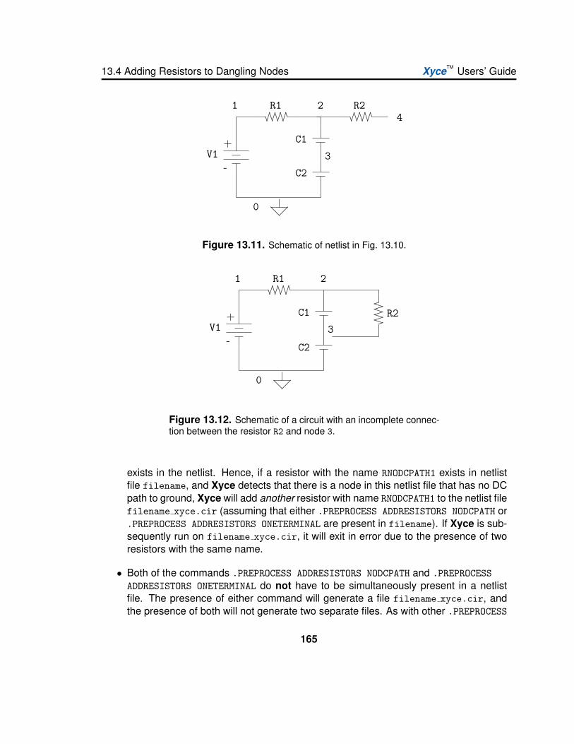
13.4 Adding Resistors to Dangling Nodes XyceTM Users’ Guide
....................................
......................................
......................................
......................................
... .........................................................................................................................................................
R1 R2
C1
C2
V1
1 2
3
4
0
-
+
............................................
........
Figure 13.11. Schematic of netlist in Fig. 13.10.
....................................
......................................
......................................
......................................
...
.........................................................................................................................................................
R1
C1
C2
V1
1 2
3
0
R2
-
+
............................................
........
Figure 13.12. Schematic of a circuit with an incomplete connec-tion between the resistor R2 and node 3.
exists in the netlist. Hence, if a resistor with the name RNODCPATH1 exists in netlistfile filename, and Xyce detects that there is a node in this netlist file that has no DCpath to ground, Xyce will add another resistor with name RNODCPATH1 to the netlist filefilename xyce.cir (assuming that either .PREPROCESS ADDRESISTORS NODCPATH or.PREPROCESS ADDRESISTORS ONETERMINAL are present in filename). If Xyce is sub-sequently run on filename xyce.cir, it will exit in error due to the presence of tworesistors with the same name.
• Both of the commands .PREPROCESS ADDRESISTORS NODCPATH and .PREPROCESSADDRESISTORS ONETERMINAL do not have to be simultaneously present in a netlistfile. The presence of either command will generate a file filename xyce.cir, andthe presence of both will not generate two separate files. As with other .PREPROCESS
165
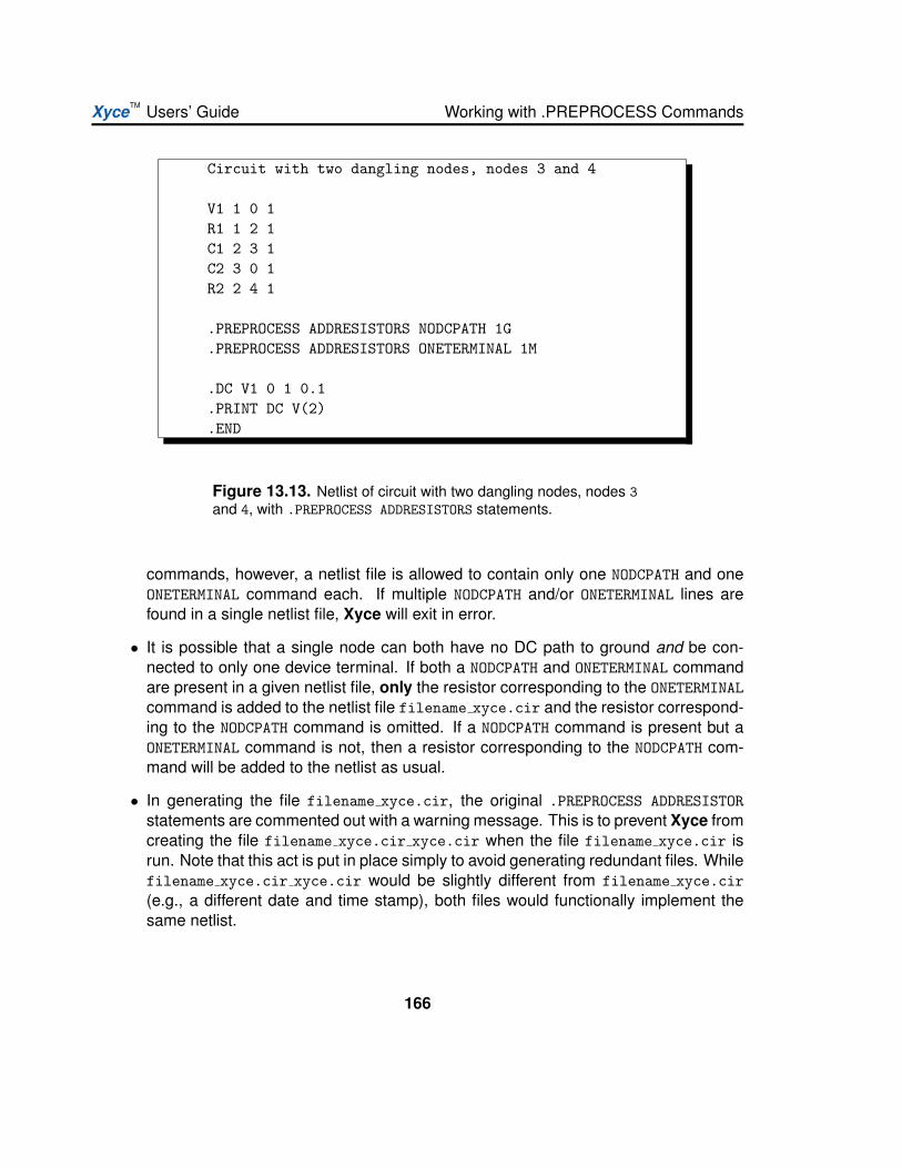
XyceTM Users’ Guide Working with .PREPROCESS Commands
Circuit with two dangling nodes, nodes 3 and 4
V1 1 0 1R1 1 2 1C1 2 3 1C2 3 0 1R2 2 4 1
.PREPROCESS ADDRESISTORS NODCPATH 1G
.PREPROCESS ADDRESISTORS ONETERMINAL 1M
.DC V1 0 1 0.1
.PRINT DC V(2)
.END
Figure 13.13. Netlist of circuit with two dangling nodes, nodes 3and 4, with .PREPROCESS ADDRESISTORS statements.
commands, however, a netlist file is allowed to contain only one NODCPATH and oneONETERMINAL command each. If multiple NODCPATH and/or ONETERMINAL lines arefound in a single netlist file, Xyce will exit in error.
• It is possible that a single node can both have no DC path to ground and be con-nected to only one device terminal. If both a NODCPATH and ONETERMINAL commandare present in a given netlist file, only the resistor corresponding to the ONETERMINALcommand is added to the netlist file filename xyce.cir and the resistor correspond-ing to the NODCPATH command is omitted. If a NODCPATH command is present but aONETERMINAL command is not, then a resistor corresponding to the NODCPATH com-mand will be added to the netlist as usual.
• In generating the file filename xyce.cir, the original .PREPROCESS ADDRESISTORstatements are commented out with a warning message. This is to prevent Xyce fromcreating the file filename xyce.cir xyce.cir when the file filename xyce.cir isrun. Note that this act is put in place simply to avoid generating redundant files. Whilefilename xyce.cir xyce.cir would be slightly different from filename xyce.cir(e.g., a different date and time stamp), both files would functionally implement thesame netlist.
166

13.4 Adding Resistors to Dangling Nodes XyceTM Users’ Guide
XYCE-generated Netlist file copy: TIME=’07:32:31 AM’* DATE=’Dec 19, 2007’*Original Netlist Title:
*Circuit with two dangling nodes, nodes 3 and 4
V1 1 0 1R1 1 2 1C1 2 3 1C2 3 0 1R2 2 4 1
*.PREPROCESS ADDRESISTORS NODCPATH 1G*Xyce: ".PREPROCESS ADDRESISTORS" statement* automatically commented out in netlist copy.*.PREPROCESS ADDRESISTORS ONETERMINAL 1M*Xyce: ".PREPROCESS ADDRESISTORS" statement* automatically commented out in netlist copy.
.DC V1 0 1 0.1
.PRINT DC V(2)
*XYCE-GENERATED OUTPUT: Adding resistors between ground* and nodes connected to only 1 device terminal:
RONETERM1 4 0 1M
*XYCE-GENERATED OUTPUT: Adding resistors between ground* and nodes with no DC path to ground:
RNODCPATH1 3 0 1G
.END
Figure 13.14. Output file filename xyce.cir which results fromthe .PREPROCESS ADDRESISTOR statements for the netlist of Fig.13.12 (with assumed file name filename).
167

XyceTM Users’ Guide Working with .PREPROCESS Commands
....................................
......................................
......................................
......................................
... .........................................................................................................................................................
....................
........................................
........................................
........................................
.........................................................................
........................................
........................................
.............
R1 R2
C1
C2
V1 3
4
0
1G
1M
1 2
-
+
............................................
........
Figure 13.15. Schematic corresponding to the Xyce-generatednetlist of Fig. 13.14.
168

14. TCAD (PDE Device)Simulation with Xyce
Chapter OverviewThis chapter gives guidance on how to use the mesh-based device simulation capability ofXyce. It includes the following sections:
Section 14.1, Introduction
Section 14.2, One Dimensional Example
Section 14.3, Two Dimensional Example
Section 14.4, Doping Profile
Section 14.5, Electrodes
Section 14.6, Meshing
Section 14.7, Mobility Models
Section 14.8, Bulk Materials
Section 14.9, Solver Options
Section 14.10, Output and Visualization
169

XyceTM Users’ Guide TCAD (PDE Device) Simulation with Xyce
14.1 Introduction
This chapter describes how to use the mesh-based device simulation functionality of Xyce.This capability is based on the solution a coupled set of partial differential equations(PDEs), discretized on a mesh such as the one in Figure 14.1. Such devices are oftenreferred to as TCAD devices, where TCAD stands for Technology Computer Aided Design.While the rest of Xyce is intended to be similar to analog circuit simulators such as SPICE,the TCAD device capability is intended to be similar to well-known device simulators suchas PISCES [18] and DaVinci [19].
Two different TCAD devices are available Xyce: a one-dimensional device and a two-dimensional device. These two devices have been implemented in a manner which allowsthem to be invoked in the same way as a conventional lumped parameter circuit device.Generally, this capability is intended for very detailed simulation of semiconductor devices,such as diodes, bipolar transistors, and MOSFETs. One possible application of this ca-pability is the evaluation and/or analysis of conventional SPICE-style lumped parametermodels.
NOTE: As of Xyce Release 2.1, the TCAD devices should still be considered to be a beta-level capability. The primary focus of Xyce has been traditional analog circuit simulation,so the TCAD devices have not been subject to the same level of testing as the traditional,SPICE-style devices. The TCAD (PDE) device simulator in Xyce should be regarded as aprototype for Charon, a high performance 3D device simulator that is under developmentat Sandia.
NOTE: The use of square brackets [] in the doping and electrode specifications is no longercorrect as of Xyce Release 2.1. The correct delimiter to use for these parameters is nowthe curly bracket .
Equations
The equations of device simulation are described by many references including Kramer [20]and Selberherr [21]. The most common formulation, and the one that is used in Xyce, isthe drift-diffusion (DD) formulation. This formulation consists of three coupled PDE’s: asingle Poisson equation for electrostatic potential and two continuity equations; one eachfor electrons and holes.
170
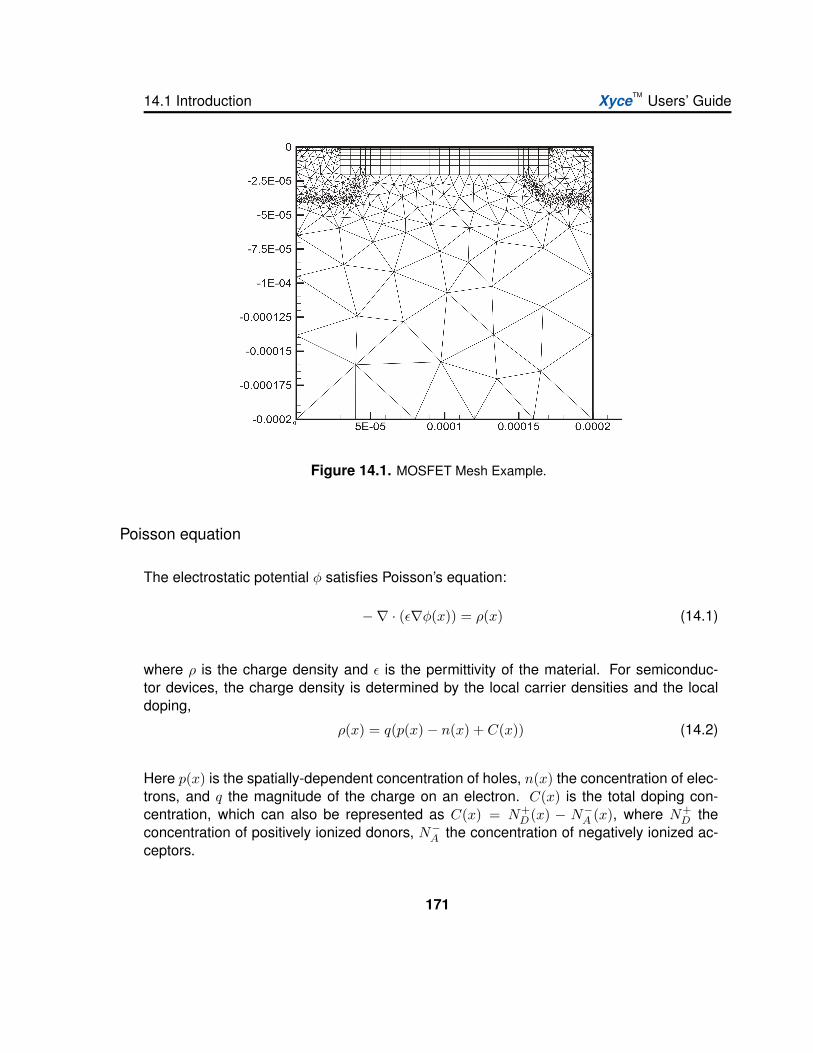
14.1 Introduction XyceTM Users’ Guide
Figure 14.1. MOSFET Mesh Example.
Poisson equation
The electrostatic potential φ satisfies Poisson’s equation:
−∇ · (ε∇φ(x)) = ρ(x) (14.1)
where ρ is the charge density and ε is the permittivity of the material. For semiconduc-tor devices, the charge density is determined by the local carrier densities and the localdoping,
ρ(x) = q(p(x)− n(x) + C(x)) (14.2)
Here p(x) is the spatially-dependent concentration of holes, n(x) the concentration of elec-trons, and q the magnitude of the charge on an electron. C(x) is the total doping con-centration, which can also be represented as C(x) = N+
D (x) − N−A (x), where N+
D theconcentration of positively ionized donors, N−
A the concentration of negatively ionized ac-ceptors.
171
XyceTM Users’ Guide TCAD (PDE Device) Simulation with Xyce
Species continuity equations
The continuity equations relate the convective derivative of the species concentrations tothe creation and destruction of particles (“recombination/generation”).
∂n(x)∂t
+∇ · Γn = −R(x) (14.3)
∂p(x)∂t
+∇ · Γp = −R(x) (14.4)
Here n is the electron concentration and p is the hole concentration. R is the recombinationrate for both species. Γn and Γp are particle fluxes for electrons and holes, respectively.The sign of R is chosen because R is usually expressed as a recombination rate, andis positive if particles are annihilating. The right hand sides are equal since creation anddestruction of carriers occurs in pairs.
One way in which the drift-diffusion model differs from other common formulations is themanner in which the quantities Γn and Γp are determined. The expressions used are:
Γn = n(x)µnE(x) + Dn∇n(x) (14.5)Γp = p(x)µpE(x) + Dp∇p(x) (14.6)
Here µn, µp are mobilities for electrons and holes, and Dn, Dp are diffusion constants.E(x) is the electric field, which is given by the gradient of the potential, or −∂φ/∂x.
Discretization
Xyce uses a box-integration discretization, with the Scharfetter-Gummel method for model-ing the flux of charged species. This method has been described in detail elsewhere [20] [21] [22],so it will not be described here.
172
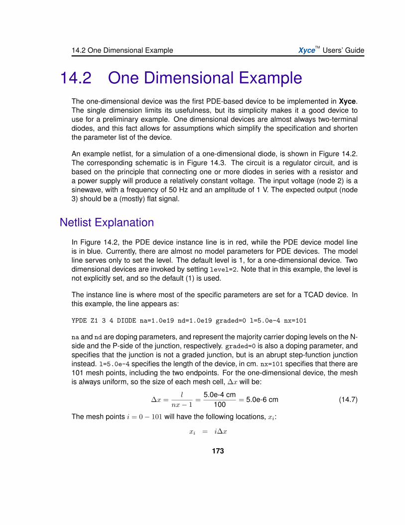
14.2 One Dimensional Example XyceTM Users’ Guide
14.2 One Dimensional ExampleThe one-dimensional device was the first PDE-based device to be implemented in Xyce.The single dimension limits its usefulness, but its simplicity makes it a good device touse for a preliminary example. One dimensional devices are almost always two-terminaldiodes, and this fact allows for assumptions which simplify the specification and shortenthe parameter list of the device.
An example netlist, for a simulation of a one-dimensional diode, is shown in Figure 14.2.The corresponding schematic is in Figure 14.3. The circuit is a regulator circuit, and isbased on the principle that connecting one or more diodes in series with a resistor anda power supply will produce a relatively constant voltage. The input voltage (node 2) is asinewave, with a frequency of 50 Hz and an amplitude of 1 V. The expected output (node3) should be a (mostly) flat signal.
Netlist Explanation
In Figure 14.2, the PDE device instance line is in red, while the PDE device model lineis in blue. Currently, there are almost no model parameters for PDE devices. The modelline serves only to set the level. The default level is 1, for a one-dimensional device. Twodimensional devices are invoked by setting level=2. Note that in this example, the level isnot explicitly set, and so the default (1) is used.
The instance line is where most of the specific parameters are set for a TCAD device. Inthis example, the line appears as:
YPDE Z1 3 4 DIODE na=1.0e19 nd=1.0e19 graded=0 l=5.0e-4 nx=101
na and nd are doping parameters, and represent the majority carrier doping levels on the N-side and the P-side of the junction, respectively. graded=0 is also a doping parameter, andspecifies that the junction is not a graded junction, but is an abrupt step-function junctioninstead. l=5.0e-4 specifies the length of the device, in cm. nx=101 specifies that there are101 mesh points, including the two endpoints. For the one-dimensional device, the meshis always uniform, so the size of each mesh cell, ∆x will be:
∆x =l
nx− 1=
5.0e-4 cm100
= 5.0e-6 cm (14.7)
The mesh points i = 0− 101 will have the following locations, xi:
xi = i∆x
173
XyceTM Users’ Guide TCAD (PDE Device) Simulation with Xyce
PDE Diode Regulator CircuitVP 1 0 PULSE(0 5 0.0 2.0e-2 0.0 1.0e+20 1.2e+20)VF 2 1 SIN(0 1 50 2.0e-2)VT1 4 0 0VR1 2 3 1k
* TCAD/PDE DeviceYPDE Z1 3 4 DIODE na=1.0e19 nd=1.0e19 graded=0+ l=5.0e-4 nx=101
.MODEL DIODE ZOD
.TRAN 1.0e-3 12.0e-2
.print TRAN format=tecplot+ v(1) v(2) v(3) v(4) I(VF) I(VT1)
.options NONLIN maxstep=100 maxsearchstep=3+ searchmethod=2 nox=1
.options TIMEINT reltol=1.0e-3 abstol=1.0e-6
.END
Figure 14.2. One dimensional diode netlist. This circuit is avoltage regulator. The input signal should be a sinewave, whilethe output signal should be nearly flat. For the result of this netlist,see Figure 14.4
174

14.2 One Dimensional Example XyceTM Users’ Guide
Figure 14.3. Voltage regulator schematic. The diode, Z1, is thePDE device in this example.
xo = 0.0 cmx1 = 5.0e-6 cm
.
.
.
x101 = 5.0e-4 cm
Boundary Conditions and Doping Profile
Note that nothing has been specified in the example netlist about electrodes, or boundaryconditions, and that the doping specification is minimal. This is because the example reliesa lot on default parameters. A one dimensional device can only have exactly 2 electrodesconnected to the circuit. These two electrodes are at opposite ends of the domain, one atthe first mesh point (x=0.0 cm, i=0) and the other at the opposite end of the domain, at thelast mesh point (x=5.0e-4 cm, i=101).
The electrode associated with the first mesh point (x=0.0 cm) is connected to the secondcircuit node on the instance line, while the electrode associated with the last mesh point(x=l) is connected to the first circuit node on the instance line. For the doping used inthis example, the junction is in the exact center of the device (x=l/2), and the n-side is
175

XyceTM Users’ Guide TCAD (PDE Device) Simulation with Xyce
the region defined by x<l/2, and the p-side is the region defined by x>l/2. This defaultdoping, along with the electrode-circuit connectivity, result in the one-dimensional deviceto behave like a traditional SPICE-style diode. For a complete discussion of how to specifya doping profile see section 14.4. For a complete discussion of how to specify electrodesin detail (including boundary conditions), see section 14.5.
Results
The transient result of this circuit is shown in Figure 14.4. The input signal (node 2) isrepresented by the blue line, and the output signal (node 3) is represented by the red line.The voltage drop across the diode is nearly the same for a wide range of currents, and isapproximately 0.67 V. The voltage drop across the series resistor, R1, is much more sensi-tive to the current magnitude, and so most of the voltage variation of the input sinewave isaccounted for by R1.
176
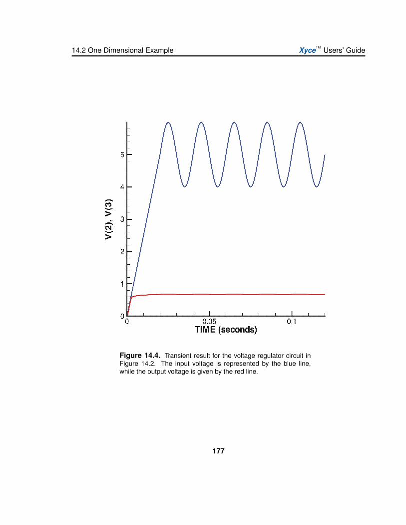
14.2 One Dimensional Example XyceTM Users’ Guide
Figure 14.4. Transient result for the voltage regulator circuit inFigure 14.2. The input voltage is represented by the blue line,while the output voltage is given by the red line.
177

XyceTM Users’ Guide TCAD (PDE Device) Simulation with Xyce
14.3 Two Dimensional ExampleAn example netlist, for a simulation of a two-dimensional bipolar transistor, is shown inFigure 14.5. As before, the PDE device instance line is in red, while the PDE device modelline is in blue. In this case, note that the level has been specified on the model line, and ithas been set to 2. This is required for the two-dimensional device. This particular exampleis a DC sweep of a bipolar transistor device. A schematic, illustrating this circuit is shownin Figure 14.6.
Netlist Explanation
The two-dimensional device can have 2-4 electrodes. (this limitation will be relaxed infuture versions of Xyce) In this example there are three; node 5, node 3 and node 7.These correspond to the three names on the ”node” line, which appears as:
+ node = name = collector, base, emitter
This line specifies that node 5 is connected to an electrode named ”collector”, node 3is connected to an electrode named ”base”, and node 7 is connected to an electrodenamed ”emitter”. Although this example only contains the electrode names, the ”node”specification can contains a lot of information. For a full explanation of all the electrodeparameters, see section 14.5.
The next line contains parameters concerned with plotting the results, and appears asfollows:
+ tecplotlevel=2 txtdatalevel=1
Note that these are not related to the output specified by .PRINT, which outputs circuit data.The tecplotlevel command enables files to be output which are readable by Tecplot.Tecplot can then be used to create contour plots of quantities such as the electron density,electrostatic potential and the doping profile. Figures 14.7 and 14.8 contain examples ofTecplot-generated contour plots, which were generated from the results of this example.
The txtdatalevel command enables a text file with volume averaged information to beoutput to a file. Currently, both of these output files will be updated at each time step or DCsweep step.
The next line, mobmodel=arora, specifies which mobility model to use. For more detail onavailable mobility models, see section 14.7.
178
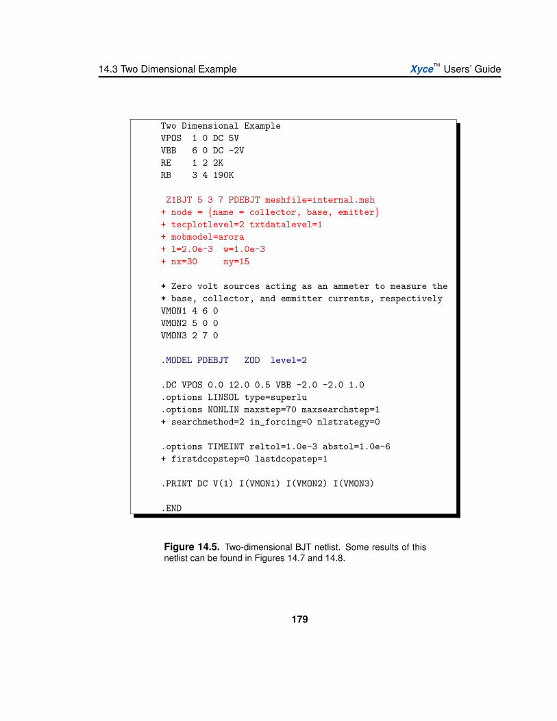
14.3 Two Dimensional Example XyceTM Users’ Guide
Two Dimensional ExampleVPOS 1 0 DC 5VVBB 6 0 DC -2VRE 1 2 2KRB 3 4 190K
Z1BJT 5 3 7 PDEBJT meshfile=internal.msh+ node = name = collector, base, emitter+ tecplotlevel=2 txtdatalevel=1+ mobmodel=arora+ l=2.0e-3 w=1.0e-3+ nx=30 ny=15
* Zero volt sources acting as an ammeter to measure the* base, collector, and emmitter currents, respectivelyVMON1 4 6 0VMON2 5 0 0VMON3 2 7 0
.MODEL PDEBJT ZOD level=2
.DC VPOS 0.0 12.0 0.5 VBB -2.0 -2.0 1.0
.options LINSOL type=superlu
.options NONLIN maxstep=70 maxsearchstep=1+ searchmethod=2 in_forcing=0 nlstrategy=0
.options TIMEINT reltol=1.0e-3 abstol=1.0e-6+ firstdcopstep=0 lastdcopstep=1
.PRINT DC V(1) I(VMON1) I(VMON2) I(VMON3)
.END
Figure 14.5. Two-dimensional BJT netlist. Some results of thisnetlist can be found in Figures 14.7 and 14.8.
179

XyceTM Users’ Guide TCAD (PDE Device) Simulation with Xyce
The last two lines, specify the mesh of the device, and are given by:
+ l=2.0e-3 w=1.0e-3+ nx=30 ny=15
This numbers are used in nearly the same way as the l and nx parameters were used inthe one-dimensional case. The mesh is Cartesian, and the spacing is uniform.
Doping Profile
As in the one-dimensional example, the two-dimensional example in Figure 14.5 does notspecify anything about the doping profile, and thus relies upon defaults. In this case thereare three specified electrodes, which by default results in the doping profile of the bipolarjunction transistor (BJT). For a complete description of how to specify a doping profile indetail, see section 14.4. This section also describes the various default impurity profiles.
Boundary Conditions and Electrode Configuration
As in the one-dimensional example, the two-dimensional example in Figure 14.5 does notspecify anything about the electrode configuration or the boundary conditions, and relieson default settings. To be consistent with the default 3-terminal doping, the device hasterminals that correspond to that of a BJT. All three electrodes (collector, base, emitter) arealong the top of the device.
By default all electrodes are considered to be neutral contacts. The boundary conditionsapplied to the electron density, hole density and electrostatic potential are all Dirichletconditions.
For a complete discussion of how to specify electrodes in detail (including boundary con-ditions), see section 14.5.
Results
Results for the two-dimensional example can be found in Figures 14.7, 14.8 and 14.9. Thefirst two figures are contour plots of the electrostatic potential. The first one correspondsto the first DC sweep step, where VPOS is set to 0.0 Volts. The second one correspondsto the final DC sweep step, in which VPOS has a value of 12.0 volts. The voltage source
180

14.3 Two Dimensional Example XyceTM Users’ Guide
VPOS applies a voltage to the emitter load resistor, RE, so some of the 12.0V is droppedacross RE, an the rest is applied to the BJT.
The third figure is an I-V curve of the dependence of the three terminal currents on appliedemitter voltage. For the entire sweep, a negative voltage of 2.0 V has been applied to thebase load resistor, and as this transistor is a PNP transistor, this results in the transistorbeing in an “on” state. The emitter-collector current varies nearly linearly with the appliedemitter voltage. Also, the three currents sum to nearly zero, which one would expectbecause of current conservation.
Note that the mesh is visible in Figure 14.7, and was generated using the internal “uniformmesh” option. Generally using this sort of mesh will work numerically, in that Xyce willconverge to an answer. However, this mesh will probably not produce a very accurateresult, as it does not resolve the depletion regions very well. In order to obtain betteraccuracy, either a finer uniform mesh would need to be used, or a nonuniform mesh,refined in around the depletion regions should be used. As described in section 14.6,refined, nonuniform meshes must be read in from an external mesh generator, such as theSGFramework [20].
181

XyceTM Users’ Guide TCAD (PDE Device) Simulation with Xyce
Figure 14.6. Two-Dimensional BJT Circuit Schematic. Thisschematic is for the circuit described by the netlist in Figure 14.5.The mesh in the large circle is the mesh used in the example. Theother mesh, which contains some mesh refinement, is included inthe figure as an example of what is possible with an external meshgenerator.
182
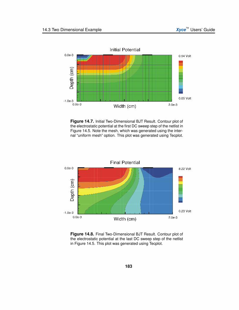
14.3 Two Dimensional Example XyceTM Users’ Guide
Figure 14.7. Initial Two-Dimensional BJT Result. Contour plot ofthe electrostatic potential at the first DC sweep step of the netlist inFigure 14.5. Note the mesh, which was generated using the inter-nal “uniform mesh” option. This plot was generated using Tecplot.
Figure 14.8. Final Two-Dimensional BJT Result. Contour plot ofthe electrostatic potential at the last DC sweep step of the netlistin Figure 14.5. This plot was generated using Tecplot.
183
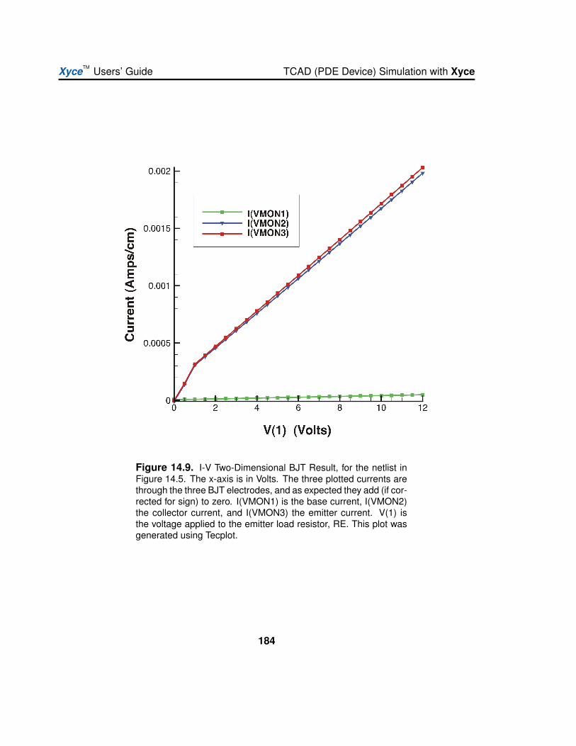
XyceTM Users’ Guide TCAD (PDE Device) Simulation with Xyce
Figure 14.9. I-V Two-Dimensional BJT Result, for the netlist inFigure 14.5. The x-axis is in Volts. The three plotted currents arethrough the three BJT electrodes, and as expected they add (if cor-rected for sign) to zero. I(VMON1) is the base current, I(VMON2)the collector current, and I(VMON3) the emitter current. V(1) isthe voltage applied to the emitter load resistor, RE. This plot wasgenerated using Tecplot.
184
14.4 Doping Profile XyceTM Users’ Guide
14.4 Doping Profile
In the two examples, no doping parameters were specified, and Xyce used the defaults.Default profiles are uniquely specified by the number of electrodes. In practice, especiallyfor two-dimensional simulations, the user will generally need to specify the doping profilemanually.
NOTE: If an external mesh (from the SGFramework) is used, the doping profile will be readin from the mesh file, and it is not necessary (or appropriate) to specify any doping in thenetlist.
Manually Specifying the Doping
A circuit netlist, which includes a one-dimensional device with a detailed, manual specifi-cation of the doping profile, is given in Figure 14.10. A similar, two-dimensional, versionof this problem is given in Figure 14.12. For the purposes of this discussion, the one-dimensional example will be referred to, but information conveyed is equally applicable tothe two-dimensional case.
In both examples, the parameters associated with doping are in red font. The doping isspecified with one or more regions, which are summed together to get the total profile.Doping regions are specified in a tabular format, with each column representing a differentregion.
In the one-dimensional example, there are three regions, which are illustrated in Fig-ure 14.11. Region 1 is a uniform n-type doping, with a constant magnitude of 4.0e+12donors per cubic cm. This magnitude is set by the parameter nmax. As the doping in thisregion is spatially uniform, the only meaningful parameters are function (which in thiscase specifies a spatially uniform distribution), type (ntype or ptype) and nmax. The otherparameters, nmin through flatx (1D) or flaty (2D), are ignored for a spatially uniformregion.
Region 2 is a more complicated region, in that the profile varies with space. This regionis doped with p-type impurities, and has a Gaussian shape. Semiconductor processingoften consists of an implant followed by an anneal, which results in a diffusive profile.The Gaussian function is a solution to the diffusion problem, when it is assumed that theimpurity exists in a fixed quantity. Thus, the Gaussian shape is an appropriate choice forthe doping regions of a lot of devices.
185
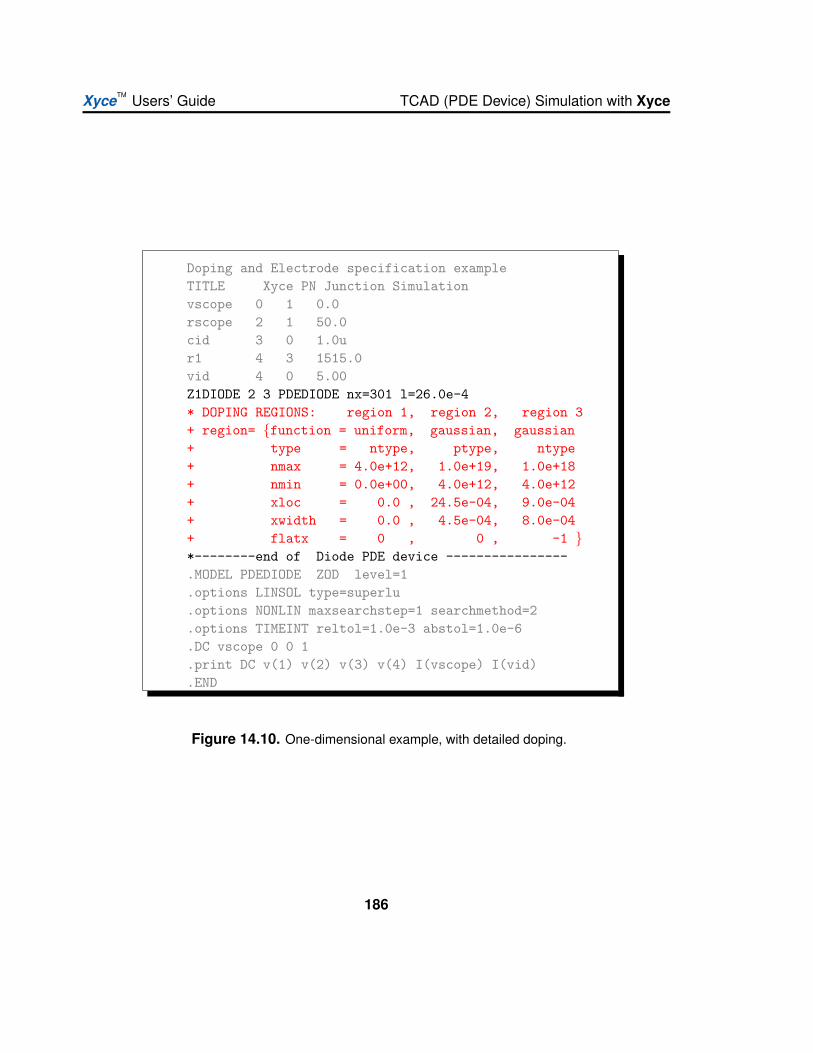
XyceTM Users’ Guide TCAD (PDE Device) Simulation with Xyce
Doping and Electrode specification exampleTITLE Xyce PN Junction Simulationvscope 0 1 0.0rscope 2 1 50.0cid 3 0 1.0ur1 4 3 1515.0vid 4 0 5.00Z1DIODE 2 3 PDEDIODE nx=301 l=26.0e-4* DOPING REGIONS: region 1, region 2, region 3+ region= function = uniform, gaussian, gaussian+ type = ntype, ptype, ntype+ nmax = 4.0e+12, 1.0e+19, 1.0e+18+ nmin = 0.0e+00, 4.0e+12, 4.0e+12+ xloc = 0.0 , 24.5e-04, 9.0e-04+ xwidth = 0.0 , 4.5e-04, 8.0e-04+ flatx = 0 , 0 , -1 *--------end of Diode PDE device ----------------.MODEL PDEDIODE ZOD level=1.options LINSOL type=superlu.options NONLIN maxsearchstep=1 searchmethod=2.options TIMEINT reltol=1.0e-3 abstol=1.0e-6.DC vscope 0 0 1.print DC v(1) v(2) v(3) v(4) I(vscope) I(vid).END
Figure 14.10. One-dimensional example, with detailed doping.
186
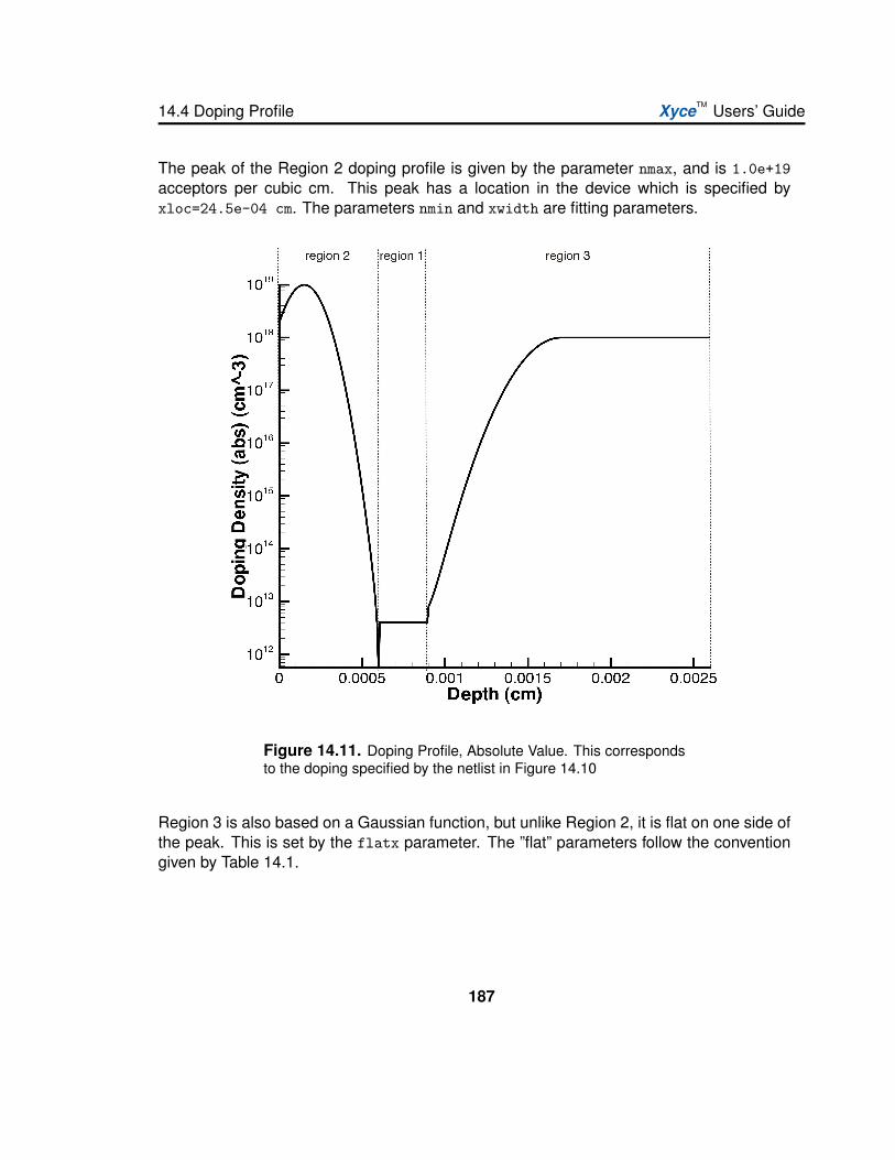
14.4 Doping Profile XyceTM Users’ Guide
The peak of the Region 2 doping profile is given by the parameter nmax, and is 1.0e+19acceptors per cubic cm. This peak has a location in the device which is specified byxloc=24.5e-04 cm. The parameters nmin and xwidth are fitting parameters.
Figure 14.11. Doping Profile, Absolute Value. This correspondsto the doping specified by the netlist in Figure 14.10
Region 3 is also based on a Gaussian function, but unlike Region 2, it is flat on one side ofthe peak. This is set by the flatx parameter. The ”flat” parameters follow the conventiongiven by Table 14.1.
187

XyceTM Users’ Guide TCAD (PDE Device) Simulation with Xyce
flatx or flaty
valueDescription 1D Cross
Section
0 Gaussian on both sides of the peak (xloc) location.
+1 Gaussian if x>xloc, flat (constant at the peak value) if
x<xloc.
-1 Gaussian if x<xloc, flat (constant at the peak value) if
x>xloc.Table 14.1: Description of the flatx, flaty doping parameters
Default Doping Profiles
Xyce has a few default doping profiles which are invoked if the user doesn’t bother tospecify detailed doping information. The default doping profiles are an artifact of earlyTCAD device development in Xyce, but are sometimes still useful. In particular, the simplestep-junction diode is often a useful canonical problem. It is convenient to invoke a stepjunction doping without having to use the more complex region tabular specification.
Most real devices will have doping profiles that do not exactly match the default profiles.When attempting to simulate a realistic device, it will be necessary to skip the defaults anduse the region tables described in the previous section.
One Dimensional Case
For the one-dimensional case, it is assumed that the doping profile is that of a simplejunction diode, with the junction location exactly in the middle. The acceptor and donorconcentrations are given by the parameters Na and Nd, respectively.
Note that the usage of Na and Nd, implicitly specifies a step junction doping profile, and ismutually exclusive with the more complex “doping region” table specification, described insection 14.4. If a netlist is input to Xyce which includes both a region table and Na (or Nd),the code will immediately exit with an error.
188
14.4 Doping Profile XyceTM Users’ Guide
Two Dimensional Case
Doping level defaults in the two dimensional case are somewhat more complicated than inthe one-dimensional case, because having two-dimensions allows for more configurations,and an arbitrary number (2-4) of electrodes. In Xyce, it was decided that the default dopingprofiles would be determined uniquely by the number of electrodes. The three availabledefault dopings are given in Table 14.2. In the case of the BJT and MOSFET dopings,it is possible to specify either n-type or p-type using the type instance parameter. If thedetailed, manual doping is used, then the type parameter is ignored.
For a two-electrode device, the default doping is that of a simple diode. The acceptorand donor doping parameters, Na and Nd are used in the same manner as in the one-dimensional device. As in the one-dimensional device, the junction is assumed to be ex-actly in the middle of the domain.
For a three-electrode device (like the example), the default doping is that of a bipolar junc-tion transistor (BJT). By default the transistor is a PNP, but by setting the instance param-eter type=NPN, an NPN transistor can be specified instead. The two-dimensional examplein section 14.3 relies on this default.
For a four-terminal device, the default doping is that of a metal-oxide-semiconductor (MOS-FET). Currently, the maximum number of electrodes is four, and no default profiles areavailable for more than four electrodes. By default this transistor is assumed to be NMOS,rather than PMOS.
Number of
ElectrodesDoping Profile
2 Step Function Diode
3 Bipolar Junction Transistor (BJT)
4 Metal-Oxide Semiconductor
Field-Effect Transistor(MOSFET)Table 14.2: Default Doping profiles for different numbers of elec-trodes
189

XyceTM Users’ Guide TCAD (PDE Device) Simulation with Xyce
14.5 ElectrodesIn the two examples, minimal electrodes were specified, and Xyce used the defaults. Inpractice, especially for two-dimensional simulations, the user will need to specify the elec-trodes in more detail.
NOTE: If an external mesh (from the SGFramework) is used, some of the electrode infor-mation (the locations, and lengths) will be specified in the mesh file, so they should not bespecified in the netlist.
Manually Specifying the Electrodes
A detailed electrode specification is specified in blue font in Figure 14.12. As with thedoping parameters, the electrode parameters are specified in a tabular format, in whicheach columns of the table specifies the parameters for a different electrode. The mostimportant parameter (for getting the code to run without immediately exiting with an error)is the name parameter. It is the only required parameter.
The number of specified electrodes must match the number of connected circuit nodes,and the order of the electrode columns, from left to right, is in the same order as the circuitnodes, also from left to right. In the example of Figure 14.12, the first electrode column,which specifies an electrode named “anode”, is connected to the circuit through circuitnode 2. Respectively, the second column, for the “cathode” electrode, is connected to thecircuit by circuit node 3.
If using an external mesh (see section 14.6), the external mesh file must have this samenumber of electrodes as well. Also, if using the external mesh, the electrode names speci-fied in the electrode table must match (case insensitive) with the electrode names used bythe external mesh.
Boundary Conditions
In the example, the bc parameter has been set to “Dirichlet” on all the electrodes, whichis the default. The bc parameter sets the type of boundary condition that is applied tothe density variables, the electron density and the hole density. There are two possiblesettings for the bc parameter, Dirichlet and Neumann. If Dirichlet is specified, the electronand hole densities are set to a specific value at the contact, and the applied values enforcecharge neutrality. See the Xyce Reference Guide for the charge-neutral equation [23].
190
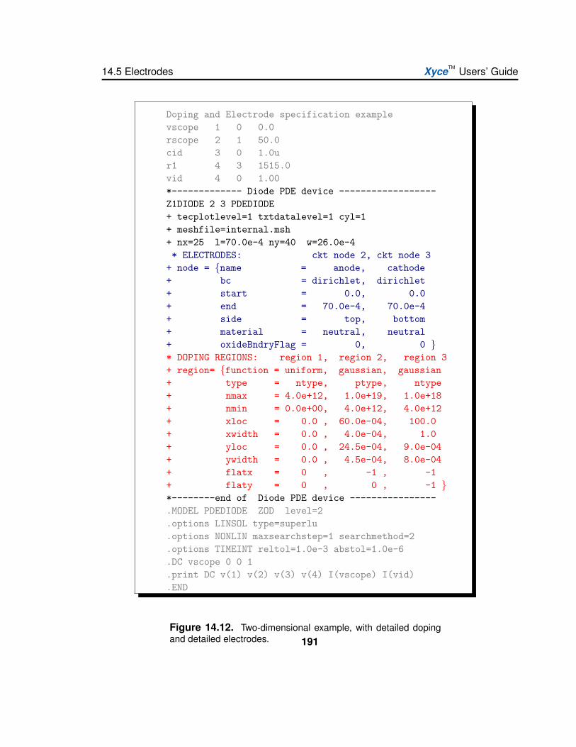
14.5 Electrodes XyceTM Users’ Guide
Doping and Electrode specification examplevscope 1 0 0.0rscope 2 1 50.0cid 3 0 1.0ur1 4 3 1515.0vid 4 0 1.00*------------- Diode PDE device ------------------Z1DIODE 2 3 PDEDIODE+ tecplotlevel=1 txtdatalevel=1 cyl=1+ meshfile=internal.msh+ nx=25 l=70.0e-4 ny=40 w=26.0e-4* ELECTRODES: ckt node 2, ckt node 3+ node = name = anode, cathode+ bc = dirichlet, dirichlet+ start = 0.0, 0.0+ end = 70.0e-4, 70.0e-4+ side = top, bottom+ material = neutral, neutral+ oxideBndryFlag = 0, 0 * DOPING REGIONS: region 1, region 2, region 3+ region= function = uniform, gaussian, gaussian+ type = ntype, ptype, ntype+ nmax = 4.0e+12, 1.0e+19, 1.0e+18+ nmin = 0.0e+00, 4.0e+12, 4.0e+12+ xloc = 0.0 , 60.0e-04, 100.0+ xwidth = 0.0 , 4.0e-04, 1.0+ yloc = 0.0 , 24.5e-04, 9.0e-04+ ywidth = 0.0 , 4.5e-04, 8.0e-04+ flatx = 0 , -1 , -1+ flaty = 0 , 0 , -1 *--------end of Diode PDE device ----------------.MODEL PDEDIODE ZOD level=2.options LINSOL type=superlu.options NONLIN maxsearchstep=1 searchmethod=2.options TIMEINT reltol=1.0e-3 abstol=1.0e-6.DC vscope 0 0 1.print DC v(1) v(2) v(3) v(4) I(vscope) I(vid).END
Figure 14.12. Two-dimensional example, with detailed dopingand detailed electrodes. 191

XyceTM Users’ Guide TCAD (PDE Device) Simulation with Xyce
If Neumann is specified, a zero-flux condition is applied, which enforces that the currentthrough the electrode will be zero.
This parameter does not affect the electrostatic potential boundary condition. The bound-ary condition applied to the potential is always Dirichlet, and is (in part) determined fromthe connected nodal voltage. To apply a specific voltage to an electrode contact, a voltagesource should be attached to it, such as VBB in the schematic Figure 14.6.
Electrode Material
Several different electrode materials can be specified. A list is given in Table 14.3. Themain effect of any metal (non-neutral) material is the impose a Schottky barrier at thecontact. This generally makes numerical solution more difficult, so any materials shouldbe applied with caution.
The Xyce Reference Guide [23] has a detailed description of Schottky barriers and howthey are imposed on contacts in Xyce. Also, values for electron affinities of various bulkmaterials and workfunction values for the various metal contacts are given in the ReferenceGuide.
Material Symbol Comments
neutral neutral Default
aluminum al
p+-polysilicon ppoly
n+-polysilicon npoly
molybdenum mo
tungsten w
molybdenum disilicide modi
tungsten disilicide wdi
copper cu
platinum pt
gold au
Table 14.3: Electrode Material Options. Neutral contacts are thedefault, and pose the least problem to the solvers.
There is also an oxideBndryFlag parameter, which if set to true (1), will model the contact
192
14.5 Electrodes XyceTM Users’ Guide
as having an oxide layer in between the metal contact and the bulk semiconductor. Bydefault, oxideBndryFlag is false (0). Note that this oxide layer model does not currentlyinclude displacement current, so transient capacitive effects will not be seen in the results.
Location Parameters
Each electrode has three location parameters: start, end, and side. These are onlynecessary if using the internal mesh and should not be specified if using an external,SGFramework mesh.
For the internal mesh, the mesh is assumed to be rectangular, and any electrode is as-sumed to be on one of the four sides. The four side possibilities are: top, bottom, rightand left. These four sides are parallel to mesh directions. The start and end parametersare floating point numbers which specify the starting and ending location of an electrode,in units of centimeters.
The lower left hand corner of the mesh rectangle is located at the origin. A side=bottomelectrode with start=0.0 and end=1.0e-4 will originate at the lower left hand corner of themesh (x=0.0, y=0.0) and end at (x=1.0e-4, y=0.0).
NOTE: Xyce will attempt to match the specified electrode to the specified mesh. However,if the user specifies a mesh that is not consistent with the electrode locations, the elec-trodes will not be able to have the exact length specified. For example, if the mesh spacingis ∆x = 1.0e-5, then the electrodes can only have a length that is a multiple of 1.0e-5.
Electrode Defaults
There are defaults for all the electrode parameters except the names. In practice, thelocations of the electrodes will usually be explicitly specified (either using the electrodetable, or as part of an external mesh file). Default electrode locations have been created tocorrespond with the default dopings, and they should only be used in that context.
Location Parameters
In practice, the locations of the electrodes will usually be explicitly specified, but they havedefaults to correspond with the default dopings. The default electrode locations in one-dimensional devices are for a diode. One electrode is located at x=xmin, while the other islocated at x=xmax.
193

XyceTM Users’ Guide TCAD (PDE Device) Simulation with Xyce
The default electrode locations in two-dimensional devices are dependent on the numberof electrodes, similar to the default dopings. Table 14.2 can be used to determine theconfigurations. For the two-terminal diode, the two electrodes are along the y-axis, at thex=xmin and x=xmax extrema. For the three-terminal BJT , all three electrodes are parallelto the x-axis, along the top, at y=ymax. For the four-terminal MOSFET, the drain, gate, andsource electrodes are also along the top, but the bulk electrode spans the entire length ofthe bottom of the mesh, at y=ymin.
194
14.6 Meshes XyceTM Users’ Guide
14.6 Meshes
Meshes from the SG Framework (External, 2D)
It is possible to have Xyce read in a two-dimensional mesh which was generated exter-nally, by the SGFramework [20]. The mesh pictured in Figure 14.1 is such a mesh, andso is the refined mesh (not inside the circle) in Figure 14.6. To use an SGF-generatedmesh, the instance parameter, ”meshfile” must be used, and set to be the name of theSGFramework-generated file. Xyce will assume that the mesh file is located in the lo-cal execution directory. One advantage of using an externally generated mesh (over aninternally generated mesh - see next section) is that external meshing tools are more so-phisticated, and in particular have mesh refinement capabilities.
Instructions for the usage of the SGFramework is outside the scope of this document. If theuser wishes to generate meshes in this manner, it is best to consult Kramer [20]. Futureversions of Xyce may accept mesh files generated by other mesh generators, such asCubit [24].
Cartesian Meshes (Internal, 1D and 2D)
One dimensional and two-dimensional devices can both create Cartesian meshes, withoutrequiring an external mesh generator. For the two-dimensional devices, it is necessaryto specify meshfile=internal.msh to invoke the Cartesian meshing capability. For one-dimensional devices, this isn’t needed, as there is no other option.
Meshes generated in this manner are very simple, in that there are only two parametersper dimension, and the resulting mesh is uniform. An example of such a mesh can be seenin Figure 14.7. The mesh spacing is determined from the following expressions:
∆x =l
nx− 1(14.8)
∆y =w
ny − 1(14.9)
This mesh specification assumes that the domain is a rectangle. Non-rectangular domainscan only be described using an external mesh program.
195
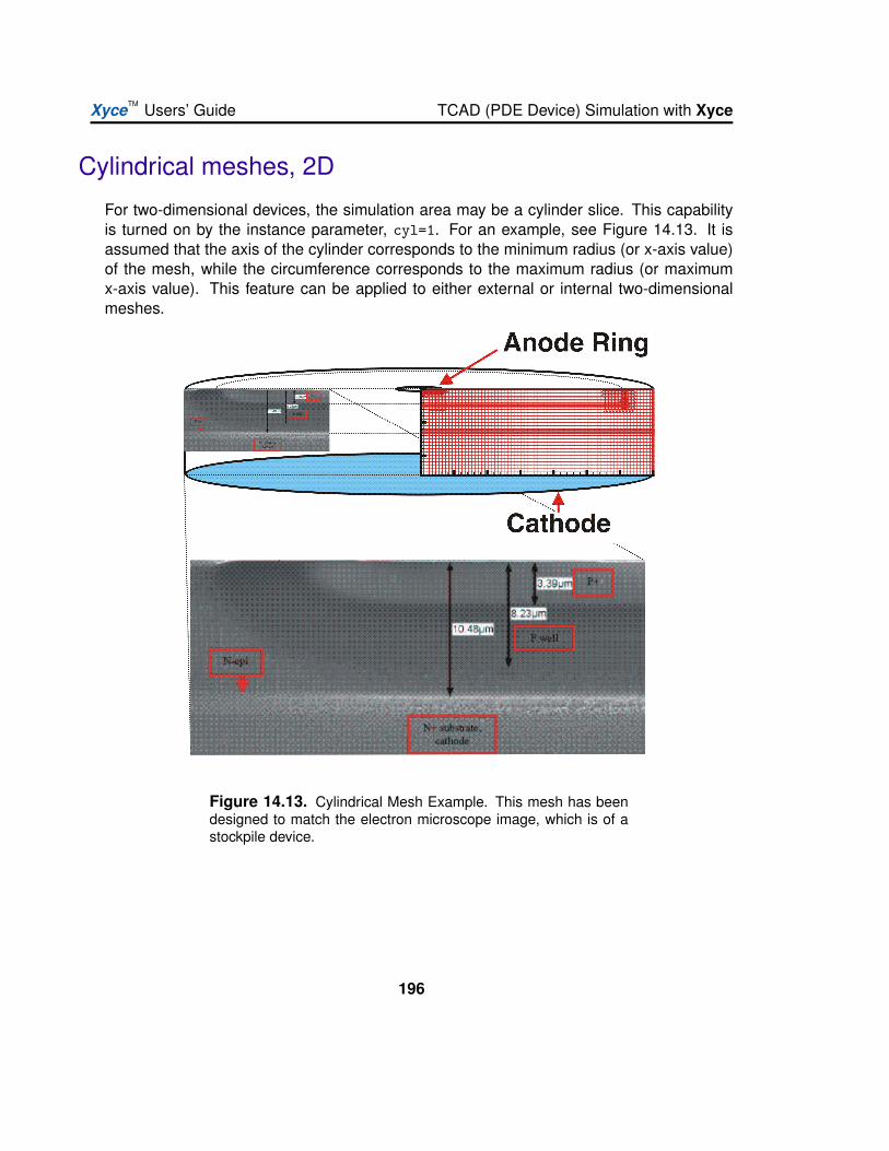
XyceTM Users’ Guide TCAD (PDE Device) Simulation with Xyce
Cylindrical meshes, 2D
For two-dimensional devices, the simulation area may be a cylinder slice. This capabilityis turned on by the instance parameter, cyl=1. For an example, see Figure 14.13. It isassumed that the axis of the cylinder corresponds to the minimum radius (or x-axis value)of the mesh, while the circumference corresponds to the maximum radius (or maximumx-axis value). This feature can be applied to either external or internal two-dimensionalmeshes.
Figure 14.13. Cylindrical Mesh Example. This mesh has beendesigned to match the electron microscope image, which is of astockpile device.
196

14.7 Mobility Models XyceTM Users’ Guide
14.7 Mobility ModelsThere are several mobility models available to both the one and two dimensional devices,and they are listed in Table 14.4. These models are fairly common, and can be found inmost device simulators. [18] [19] These models are described in more detail in the XyceReference Guide [23].
Mobility Name Description Reference
arora Basic mobility model Arora, et al. [25]
analytic Basic mobility model Caughy and Thomas [26]
carr Includes carrier-carrier
interactionsDorkel and Leturq [27]
surface Lombardi Surface Mobility
ModelLombardi, et al. [28]
Table 14.4: Mobility models available for PDE devices
Specifying the mobility model from the netlist is done by setting the mobmodel parameter tothe name of the model. Model names are given in the first column of Table 14.4. The mo-bility model is specified as an instance parameter on the device instance line, as (typically)mobmodel=arora. See the usage in Figure 14.5 for a more detailed example.
The default mobility is the ”carr” mobility, which includes carrier-carrier interactions. Thismodel has a stronger dependence on carrier density than the other two models, and intro-duces some nonlinearity into the problem. If having convergence problems, consider usingeither the ”arora” or ”analytic” model, as both of these models are a little bit simpler.
197

XyceTM Users’ Guide TCAD (PDE Device) Simulation with Xyce
14.8 Bulk MaterialsThe bulk material is specified using the bulkmaterial instance parameter. Xyce currentlysupports Silicon (si) as a bulk material and this is the default. It can also simulate Gal-lium Arsenide (gaas) and Germanium (ge), but these materials have not been extensivelytested.
The mobility models described in the previous section each support all three materials,and the dielectric permittivity is correct for all three, but the carrier lifetime models may notbe. These issues will be resolved in a future Xyce release.
198
14.9 Solver Options XyceTM Users’ Guide
14.9 Solver OptionsProblems that are based on TCAD/PDE devices have different optimal solver settings thando analog circuit problems. Generally, as these devices are mesh-based, and have a morepredictable topology, iterative linear solvers have a better chance of being successful thanthey do for analog circuit simulation. Note that if using a direct solver (klu, superlu, orksparse), the best option is superlu, because ksparse and klu have both been optimizedfor circuits (not mesh-based PDE problems), while superlu is more general.
On the nonlinear solver level, voltage limiting doesn’t have an obvious application to PDEdevices, and quadratic line search appears to be the best algorithm. The solver optionsspecified in the example netlist Figure 14.5 are adequate for simulations that have a simple(linear) circuit attached.
For problems which involve a complicated external circuit, it is best to apply the two-levelNewton algorithm to the nonlinear solve. This algorithm is described in detail in Keiter [15]and Mayaram [16]. An overview of this algorithm, as applied to powenode parasitics, canbe found in section 11.2, and examples on how to use this algorithm are in section 11.3.
199
XyceTM Users’ Guide TCAD (PDE Device) Simulation with Xyce
14.10 Output and Visualization
Using the .PRINT Command
For simple plots (such as I-V curves), output results for Xyce can be generated with the.PRINT statement, which is described in detail in section 9.1. Figures 14.4 and 14.9 areexamples of the kind of data that is produced with .PRINT statement netlist commands.These particular figures were plotted in Tecplot, but many other plotting programs wouldalso have worked, including XDAMP [29].
Multi-dimensional Plots
Device simulation has visualization needs which go beyond that of conventional circuitsimulation. Multi-dimensional perspective and/or contour plots are often desirable. Xyceis capable of outputting multi-dimensional plot data in several formats, including Tecplot,GnuPlot, and Sgplot. Currently, the options for each of these formats can only enable ordisable the output of files, and when enabled, a new file (or a new append to an existingfile) will happen at every time step or DC sweep step. For long simulations, this mayproduce a prohibitive number of files. Currently, there is no equivalent to the .OPTIONSOUTPUT INITIAL INTERVAL command, nor does the output of plot data currently use thiscommand. Plot files are either output at every step or not at all.
For each type of plot file, the file is placed in the execution directory. Each individual deviceinstance is given a unique file, or files, and the file names are derived from the name of thePDE device instance. The instance names provides the prefix, and the file type (tecplot,gnuplot, sgplot) determines the suffix.
Tecplot Data
Tecplot is a commercial plotting program from Amtec Engineering, Inc., and is the bestchoice for creating contour plots of spatially dependent data. All of the graphical examplesin this chapter were created with Tecplot. (see Figures 14.7 and 14.8 for examples) Theoutput of Tecplot files is enabled using the instance parameter, tecplotlevel=1. If set tozero, no Tecplot files are output. If set to one, a separate Tecplot file is output for eachnonlinear solve. If set to two, a single Tecplot file, which contains data for every nonlinearsolve is created and is appended at the end of each solve.
200
14.10 Output and Visualization XyceTM Users’ Guide
By default tecplotlevel is set to one, meaning the code will, by default produce a separateTecplot file for each nonlinear solve. The suffix for Tecplot data files is *.dat. Internally, thefile is an ASCII text file. Tecplot does have a binary format, but Xyce has not yet been setup to use it.
Note that it is also possible to set tecplotlevel=2. Doing this will force Xyce to create onesingle Tecplot file, and the data from each solve will be appended to this file as a separatezone. This makes it possible to use Tecplot to create animations.
Gnuplot Data
Gnuplot is an open source plotting program, which is available on most Linux/Unix plat-forms. The parameter for this type of output is gnuplotlevel=1. This type of output file isoff (zero) by default, meaning no Gnuplot files will be output. The suffix for Gnuplot files is*Gnu.dat. Like Tecplot files, Gnuplot files are also in ASCII text format.
NOTE: Gnuplot will only work with structured Cartesian meshes. Externally created, un-structured meshes (even ones that appear Cartesian) cannot be plotted with Gnuplot.
Sgplot Data
Sgplot is the plotting program for the SGFramework [20]. The parameter for this type ofoutput is sgplotlevel=1. This type of output file is off (zero) by default. The suffix forSgplot data files is *.res. Internally this file is in binary format. Note that it is not a machine-independent file format.
Volume Averaged Data
Xyce can also output volume-averaged information for each PDE device. This is enabledby setting the instance parameter, txtdatalevel=1. It is off (zero) by default, meaning notext files with volume averaged data will be output.
201

XyceTM Users’ Guide
202
Bibliography
[1] Laurence Nagel and Ronald Rohrer. Computer analysis of nonlinear circuits, exclud-ing radiation (cancer). IEEE Journal of Solid-State Circuits, sc-6(4):166–182, 1971.
[2] Tom Quarles. Spice3f5 users’ guide. Technical report, University of California-Berkeley, Berkeley, California, 1994.
[3] Eric R. Keiter, Thomas V. Russo, Eric L. Rankin, Richard L. Schiek, Keith R. Santarelli,Heidi K. Thornquist, Deborah A. Fixel, Todd S. Coffey, and Roger P. Pawlowski.Xyce parallel electronic simulator: Reference guide, version 5.1.2. Technical ReportSAND2010-3331, Sandia National Laboratories, Albuquerque, NM, 2010.
[4] Orcad PSpice User’s Guide. Technical report, Orcad, Inc., 1998.
[5] gEDA Project Home Page.http://www.geda.seul.org/ .
[6] A. S. Grove. Physics and Technology of Semiconductor Devices. John Wiley andSons, Inc., 1967.
[7] H. A. Watts, E. R. Keiter, S. A. Hutchinson, and R. J. Hoekstra. Time integration forthe Xyce parallel electronic simulator. In ISCAS 01, October 2000.
[8] K.E. Brenan, S.L Campbell, and L.R. Petzold. Numerical Solution of Initial-ValueProblems in Differential-Algebraic Equations. Society for Industrial and Applied Math-matics, Philadelphia, 1996.
[9] T. Mei T. Coffey S. Hutchinson and J. Roychowdhury. Robust, stable time-domainmethods for solving mpdes of fast/slow systems. In Proc. IEEE Design AutomationConference, 2004.
[10] Ljiljunu Trujkovit, Robert C. Melville, and Sun-Chin Fang. Passivity and no-gain prop-erties establish global convergence of a homotopy method for dc operating points.Proceedings - IEEE International Symposium on Circuits and Systems, 2:914–917,1990.
203

XyceTM Users’ Guide BIBLIOGRAPHY
[11] Robert C. Melville, Ljiljana Trajkovic, San-Chin Fang, and Layne T. Watson. Artificialparameter homotopy methods for the dc operating point problem. IEEE Transactionson Computer-Aided Design of Integrated Circuits and Systems, 12(6):861–877, 1993.
[12] J. Roychowdhury. Private Communication, 2003.
[13] Heidi K. Thornquist, Eric R. Keiter, Robert J. Hoekstra, David M. Day, and Erik G. Bo-man. A parallel preconditioning strategy for efficient transistor-level circuit simulation.In ICCAD ’09: Proceedings of the 2009 International Conference on Computer-AidedDesign, pages 410–417, New York, NY, USA, 2009. ACM.
[14] Erik Boman, Karen Device, Robert Heaphy, Bruce Hendrickson, William F. Mitchell,Matthew St. John, and Courtenay Vaughan. Zoltan: Data-Management Services forParallel Applications:User’s Guide. http://www.cs.sandia.gov/zoltan, 2004.
[15] Eric R. Keiter, Scott A. Hutchinson, Robert J. Hoekstra, Eric L. Rankin, Thomas V.Russo, and Lon J. Waters. Computational algorithms for device-circuit coupling. Tech-nical Report SAND2003-0080, Sandia National Laboratories, Albuquerque, NM, Jan-uary 2003.
[16] Kartikeya Mayaram and Donald O. Pederson. Coupling algorithms for mixed-level cir-cuit and device simulation. IEEE Transactions on Computer Aided Design, II(8):1003–1012, 1992.
[17] David A. Johns and Ken Martin. Analog Integrated Circuit Design. John Wiley & Sons,Inc., 1997.
[18] Z. Yu, D. CHen, L. So, and R. W. Dutton. Pisces-2et–two dimensional device simula-tion for silicon and heterostructures. Technical report, Stanford University, 1994.
[19] Davinci User’s Manual. Technical report, TCAD Business Unit, Avanti! Corporation,1998.
[20] Kevin M. Kramer and W. Nicholas G. Hitchon. Semiconductor Devices: A SimulationApproach. Prentice-Hall, Upper Saddle River, New Jersey, 1997.
[21] S. Selberherr. Analysis and Simulation of Semiconductor Devices. Springer-Verlag,New York, 1984.
[22] Eric R. Keiter, Scott A. Hutchinson, Robert J. Hoekstra, Eric L. Rankin, Thomas V.Russo, and Lon J. Waters. Computational algorithms for device-circuit coupling. Tech-nical Report SAND2003-0080, Sandia National Laboratories, Albuquerque, NM, Jan-uary 2003.
204

BIBLIOGRAPHY XyceTM Users’ Guide
[23] Eric R. Keiter, Thomas V. Russo, Eric L. Rankin, Richard L. Schiek, Heidi K. Thorn-quist, Deborah A. Fixel, Todd S. Coffey, Roger P. Pawlowski, Keith R. Santarelli, andChristina E. Warrender. Xyce parallel electronic simulator: Reference guide, version5.2. Technical Report SAND2011-xxxx, Sandia National Laboratories, Albuquerque,NM, 2011.
[24] CUBIT Mesh Generation Toolsuite. http://cubit.sandia.gov.
[25] N.D. Arora, J.R. Hauser, and D.J. Roulston. Electron and hole mobilities in silicon asa function of concentration and temperature. IEEE Transactions on Electron Devices,ED-29:292–295, 1982.
[26] D.M. Caughey and R.E. Thomas. Carrier mobilities in silicon empirically related todoping and field. Proc. IEEE, 55:2192–2193, 1967.
[27] J.M. Dorkel and Ph. Leturq. Carrier mobilities in silicon semi-empirically related totemperature, doping, and injection level. Solid-State Electronics, 24(9):821–825,1981.
[28] C. Lombardi, S. Manzini, A. Saporito, and M. Vanzi. A physically based mobility modelfor numerical simulation of nonplanar devices. IEEE Transactions on Computer-AidedDesign, 7(11):1164–1170, November 1988.
[29] XDAMP Graphical User Interface. http://www.cs.sandia.gov/esimtools/xdamp.html.
205

XyceTM Users’ Guide
206
Index
.DCVOLT, 147
.IC, 147
.INCLUDE, 150
.NODESET, 149
.PREPROCESS, 155ADDRESISTORS, 162REMOVEUNUSED, 159REPLACEGROUND, 156
.SAVE, 150Xyce
running, 28running in parallel, 31, 127
.DC, 43
.HB, 101
.INCLUDE, 72
.MODEL, 54
.OP, 87
.OPTIONSLINSOL, 134OUTPUT, 93, 122RESTART, 93, 94
.PRINT, 122, 123DC, 43FORMAT, 124TRAN, 45, 122
.STEP, 95
.SUBCKT, 54
.TRAN, 45, 87runxyce, 27, 28runxyce.bat, 27xmpirun, 27, 28
analog behavioral modeling (ABM), 60, 77analysis
DC, 86DC sweep, 42, 86HB, 101STEP, 95transient, 45, 87
behavioral model, 54, 60analog behavioral modeling (ABM), 60,
77, 78examples, 80lookup table, 80
bias point, 86, 89bifurcation, 109
checkpoint, 93format, 93
ChileSPICE, 21circuit
elements, 50simulation, 50topology, 50, 51
command line, 28, 30options, 29output, 29
comments in a netlist, 52continuation, 109
GMIN Stepping, 116MOSFET, 111natural, 112
207

XyceTM Users’ Guide INDEX
Pseudo Transient, 116
DC analysis, 86DC Sweep, 86DC sweep, 42
OP Analysis, 87running, 87
DCOP Restart, 151device
B (nonlinear dependent) source, 78analog, 53, 54analog device summary, 56B source, 55behavioral, 78behavioral model, 54bipolar junction transistor (BJT, 55capacitor, 55current controlled current source, 55current controlled switch, 56current controlled voltage source, 55device types, 54Digital Devices, 56diode, 55independent current source, 55independent voltage source, 56inductor, 55instance, 54JFET, 55MESFET, 56MOSFET, 55mutual inductor, 55nonlinear dependent source, 55PDE Devices, 56resistor, 55ROM Devices, 56specifying ABM devices, 78subcircuit, 56transmission line, 55voltage controlled current source, 55voltage controlled switch, 55
voltage controlled voltage source, 55devices
PDE devices, 169TCAD devices, 169
Digital Devices, 56
elements, 51Example
checkpointing, 93circuit construction, 40DC sweep, 43declaring parameters, 57restarting, 94subcircuit model definition, 69, 71transient analysis, 45using expressions, 60using parameters, 58
expressions, 59additional constructs for ABM modeling,
79arithmetic functions, 62example, 60lookup table, 80operators, 61SPICE functions, 65time-dependent, 79using, 59valid constructs, 59
global nodes, 50global parameters, 58graph partitioning, 134ground nodes, 51
Harmonic Balance Analysis, 101homotopy, 109, 110
GMIN Stepping, 116MOSFET, 111natural, 112Pseudo Transient, 116
IC=, 145
208

INDEX XyceTM Users’ Guide
Initial Conditions, 143
modeldefinition, 68model interpolation, 74model organization, 72tempmodel, 74
MPI, 28, 29
netlist, 40, 50.END, 50.END statement, 40analog devices, 53, 54command elements, 53comments, 40, 52device description, 54elements, 51end line, 52expression operators, 61expressions, 59first line special, 52functions, 62, 64, 65global parameterss, 58in-line comments, 52model definition, 54node names, 51nodes, 50parameters, 56restart, 93scaling factors, 51sources, 90subcircuit, 54title, 40title line, 50, 52using expressions, 59
node names, 51nodes, 50
global, 50NOOP, 153
OP analysis, 87
output.PRINT, 122.STEP, 99comma separated value, 28log file, 28specifying file name, 28time values, 91
parallelcommunication, 133computing, 19, 20distributed-memory, 20efficiency, 20graph partitioning, 134large scale, 20load balance, 133message passing, 20MPI, 28, 29number of processors, 29shared-memory, 20
parallelGuidance, 31parameter
declaring, 57using in expressions, 58
PDE Device Modeling, 169PDE Devices, 56platforms
Apple/OSX, 29Intel X86/FreeBSD, 29Intel X86/Linux, 29Intel X86/Microsoft Windows, 29
power node parasitics, 137, 138PSpice, 21, 40
Probe, 124
Reference Guide, 21restart, 93, 94
format, 93, 94two-level, 142
resultsgraphing, 124
209

XyceTM Users’ Guide INDEX
output control, 122output frequency, 122output options, 121print commands, 123
ROM Devices, 56running Xyce, 28runxyce, 28
Sandia National Laboratories, 19schematic capture, 40solvers
iterative linear, 134transient, 91
sources, 90defining time-dependent, 90time-dependent, 90waveforms, 90
SPICE, 40, 50STEP parametric analysis, 95subcircuit
hierarchy, 70scope, 70
time stephow to select, 91maximum size, 91size, 91
topology, 51transient analysis, 45, 87two-level Newton, 137
UIC, 153Unix, 21Users of other circuit codes, 21
xmpirun, 28
ZOLTAN, 134
210

INDEX XyceTM Users’ Guide
DISTRIBUTION:
1 Wendland BeezholdIdaho Accelerator Center1500 Alvin Ricken DrivePocatello, Idaho 83201
Unless otherwise noted, all of the fol-lowing copies were distributed elec-tronically
1 MS 0316Keith Santarelli, 1412
1 MS 0316Joseph P. Castro, 1437
1 MS 0316Deborah Fixel, 1437
1 MS 0316Gary Hennigan, 1437
1 MS 0316Robert J. Hoekstra, 1437
1 MS 0316Eric R. Keiter, 1437
1 MS 0316Paul Lin, 1437
1 MS 0316Biliana Paskaleva, 1437
1 MS 0316Eric L. Rankin, 1437
1 MS 0316Thomas V. Russo, 1437
1 MS 0316Richard Schiek, 1437
1 MS 0316John N. Shadid, 1437
1 MS 0316Heidi K. Thornquist, 1437
1 MS 0321Jamesw Peery, 1400
1 MS 0321John Mitchiner, 1430
1 MS 0340Mark J. De Spain, 2123
1 MS 0344Joshua Michael Schare, 2626
1 MS 0348Markus Johannes Hoffmann,5351
1 MS 0348Garth M. Kraus, 5353
1 MS 0348George Laguna, 5351
1 MS 0348John Dye, 5351
1 MS 0351Charles Barbour, 1010
1 MS 0351H. Morgan, 1030
1 MS 0352Charles Hembree, 1344
1 MS 0352Steven D. Wix, 1734
1 MS 0352Teresa Gutierrez, 17311
211
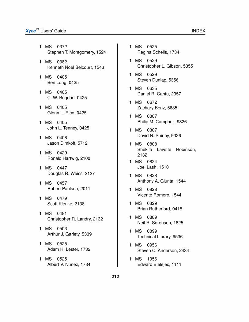
XyceTM Users’ Guide INDEX
1 MS 0372Stephen T. Montgomery, 1524
1 MS 0382Kenneth Noel Belcourt, 1543
1 MS 0405Ben Long, 0425
1 MS 0405C. W. Bogdan, 0425
1 MS 0405Glenn L. Rice, 0425
1 MS 0405John L. Tenney, 0425
1 MS 0406Jason Dimkoff, 5712
1 MS 0429Ronald Hartwig, 2100
1 MS 0447Douglas R. Weiss, 2127
1 MS 0457Robert Paulsen, 2011
1 MS 0479Scott Klenke, 2138
1 MS 0481Christopher R. Landry, 2132
1 MS 0503Arthur J. Gariety, 5339
1 MS 0525Adam H. Lester, 1732
1 MS 0525Albert V. Nunez, 1734
1 MS 0525Regina Schells, 1734
1 MS 0529Christopher L. Gibson, 5355
1 MS 0529Steven Dunlap, 5356
1 MS 0635Daniel R. Cantu, 2957
1 MS 0672Zachary Benz, 5635
1 MS 0807Philip M. Campbell, 9326
1 MS 0807David N. Shirley, 9326
1 MS 0808Shekita Lavette Robinson,2132
1 MS 0824Joel Lash, 1510
1 MS 0828Anthony A. Giunta, 1544
1 MS 0828Vicente Romero, 1544
1 MS 0829Brian Rutherford, 0415
1 MS 0889Neil R. Sorensen, 1825
1 MS 0899Technical Library, 9536
1 MS 0956Steven C. Anderson, 2434
1 MS 1056Edward Bielejec, 1111
212
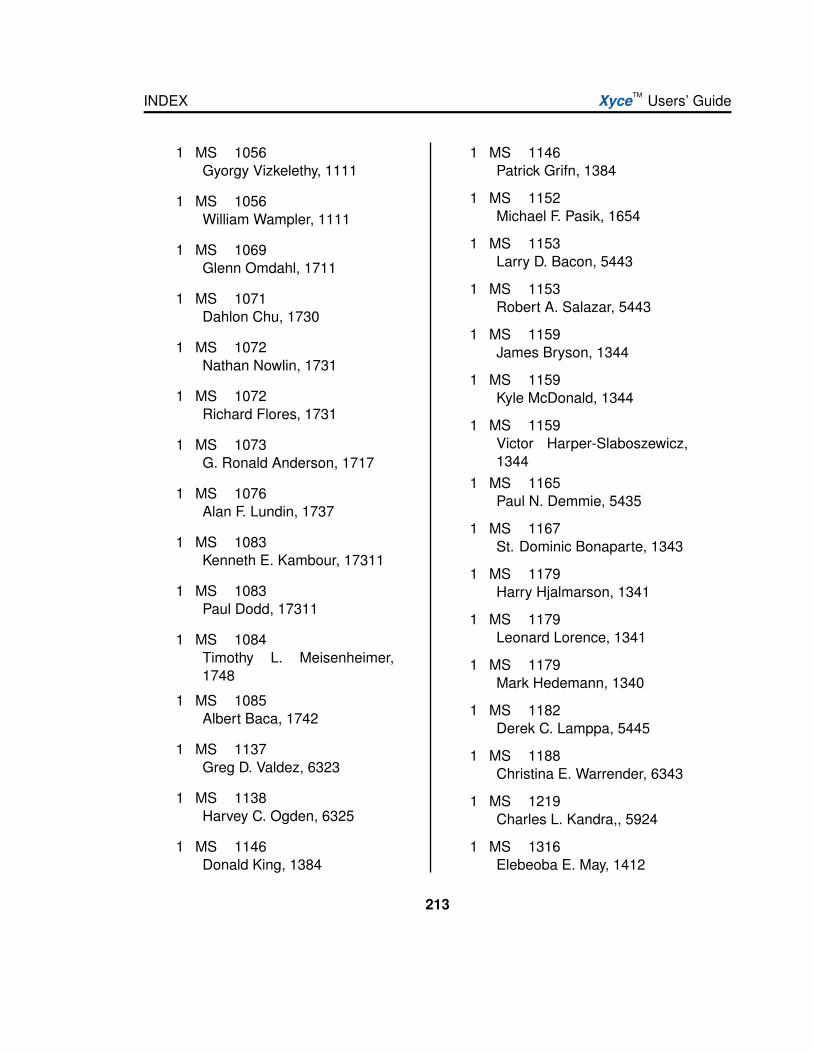
INDEX XyceTM Users’ Guide
1 MS 1056Gyorgy Vizkelethy, 1111
1 MS 1056William Wampler, 1111
1 MS 1069Glenn Omdahl, 1711
1 MS 1071Dahlon Chu, 1730
1 MS 1072Nathan Nowlin, 1731
1 MS 1072Richard Flores, 1731
1 MS 1073G. Ronald Anderson, 1717
1 MS 1076Alan F. Lundin, 1737
1 MS 1083Kenneth E. Kambour, 17311
1 MS 1083Paul Dodd, 17311
1 MS 1084Timothy L. Meisenheimer,1748
1 MS 1085Albert Baca, 1742
1 MS 1137Greg D. Valdez, 6323
1 MS 1138Harvey C. Ogden, 6325
1 MS 1146Donald King, 1384
1 MS 1146Patrick Grifn, 1384
1 MS 1152Michael F. Pasik, 1654
1 MS 1153Larry D. Bacon, 5443
1 MS 1153Robert A. Salazar, 5443
1 MS 1159James Bryson, 1344
1 MS 1159Kyle McDonald, 1344
1 MS 1159Victor Harper-Slaboszewicz,1344
1 MS 1165Paul N. Demmie, 5435
1 MS 1167St. Dominic Bonaparte, 1343
1 MS 1179Harry Hjalmarson, 1341
1 MS 1179Leonard Lorence, 1341
1 MS 1179Mark Hedemann, 1340
1 MS 1182Derek C. Lamppa, 5445
1 MS 1188Christina E. Warrender, 6343
1 MS 1219Charles L. Kandra,, 5924
1 MS 1316Elebeoba E. May, 1412
213
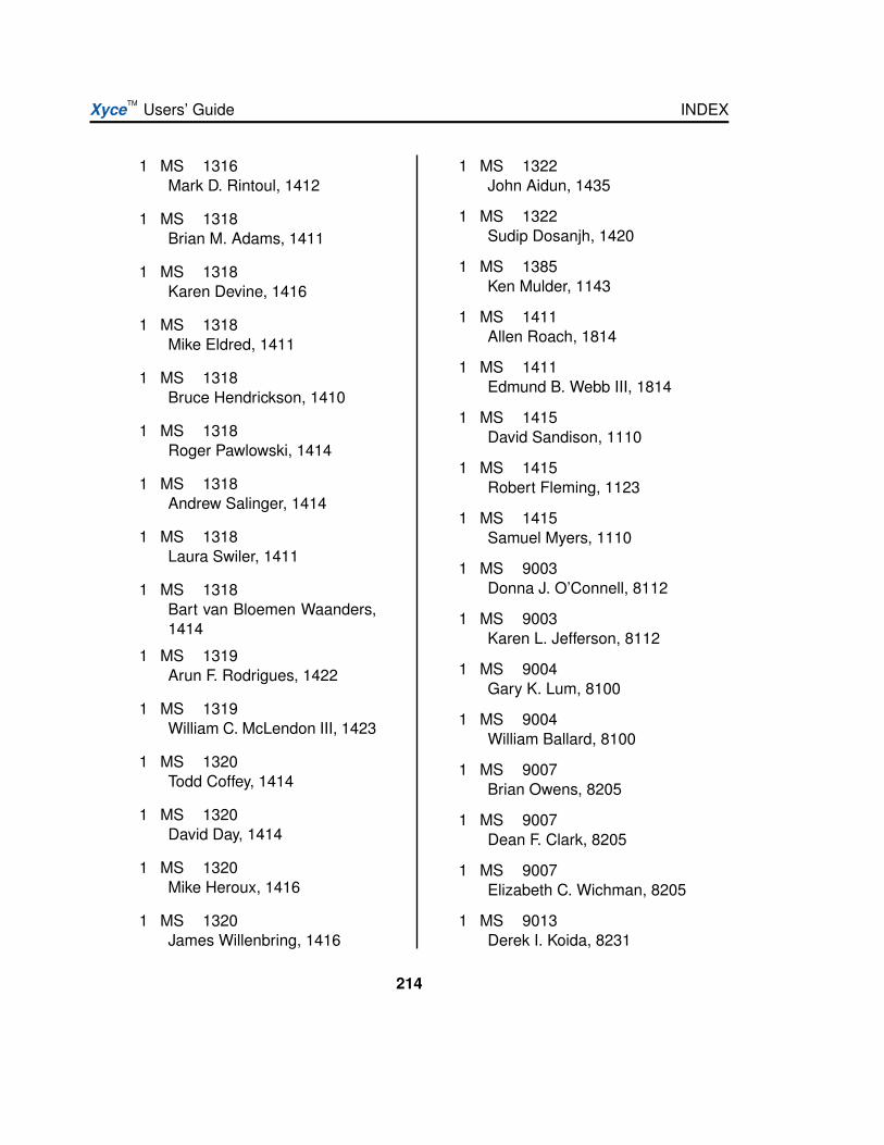
XyceTM Users’ Guide INDEX
1 MS 1316Mark D. Rintoul, 1412
1 MS 1318Brian M. Adams, 1411
1 MS 1318Karen Devine, 1416
1 MS 1318Mike Eldred, 1411
1 MS 1318Bruce Hendrickson, 1410
1 MS 1318Roger Pawlowski, 1414
1 MS 1318Andrew Salinger, 1414
1 MS 1318Laura Swiler, 1411
1 MS 1318Bart van Bloemen Waanders,1414
1 MS 1319Arun F. Rodrigues, 1422
1 MS 1319William C. McLendon III, 1423
1 MS 1320Todd Coffey, 1414
1 MS 1320David Day, 1414
1 MS 1320Mike Heroux, 1416
1 MS 1320James Willenbring, 1416
1 MS 1322John Aidun, 1435
1 MS 1322Sudip Dosanjh, 1420
1 MS 1385Ken Mulder, 1143
1 MS 1411Allen Roach, 1814
1 MS 1411Edmund B. Webb III, 1814
1 MS 1415David Sandison, 1110
1 MS 1415Robert Fleming, 1123
1 MS 1415Samuel Myers, 1110
1 MS 9003Donna J. O’Connell, 8112
1 MS 9003Karen L. Jefferson, 8112
1 MS 9004Gary K. Lum, 8100
1 MS 9004William Ballard, 8100
1 MS 9007Brian Owens, 8205
1 MS 9007Dean F. Clark, 8205
1 MS 9007Elizabeth C. Wichman, 8205
1 MS 9013Derek I. Koida, 8231
214

INDEX XyceTM Users’ Guide
1 MS 9013Lee D. Druxman, 8231
1 MS 9102David Counsil, 8229
1 MS 9102Jim He, 8135
1 MS 9102Kevin Lam, 8135
1 MS 9102Rex I. Eastin, 8135
1 MS 9103Cheryl Lam, 8942
1 MS 9106Daniel Dominguez Jr., 8226
1 MS 9106Steven Paradise, 8226
1 MS 9158Ting Mei, 1437
1 MS 9159Genetha Gray, 8964
1 MS 0899Technical Library, 9536
215