Embed Size (px)
Citation preview

Product Specification
XL160 Series 160-Watt AC to DC
Power Supplies703123 Rev 09-10-17

Notices
N2Power™ and the N2Power logo are registered trademarks of Qualstar Corporation.
Copyright© 2004-2017 by Qualstar Corporation — All Rights Reserved
For warranty information refer to www.n2power.com
N2Power products are covered by U.S. Patent 6,163,139.
Information contained in this document is copyrighted by Qualstar Corporation and is intended for use by customers and prospective customers to evaluate and integrate our power supplies. Customers and prospective customers may reproduce this document as needed for these purposes. Reproduction in whole or in part for any other purpose or by any other party is prohibited without prior written permission from Qualstar Corporation.
Every effort has been made to keep the information contained in this document current and accurate as of the date of publication or revision. However, no guarantee is given or implied that the document is error-free or that it is accurate with regard to any specification.
Qualstar reserves the right to modify the design or specification without notice. This specification may not be construed as a contractual obligation except as specifically agreed to by Qualstar in writing at the time of order.
For information about this product specification, please write or call Qualstar at:
130 West Cochran Street, Suite C Simi Valley, CA 93065
Phone: (805) 583-7744
E-Mail: [email protected] www.n2power.com
703123 Rev 09-10-17 i
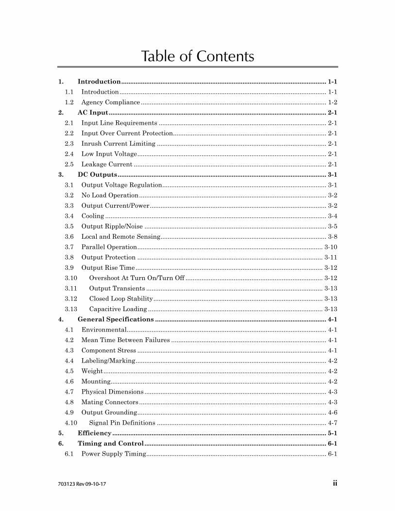
Table of Contents 1. Introduction ................................................................................................................... 1-1
1.1 Introduction .................................................................................................................... 1-1 1.2 Agency Compliance ........................................................................................................ 1-2
2. AC Input .......................................................................................................................... 2-12.1 Input Line Requirements .............................................................................................. 2-1 2.2 Input Over Current Protection ...................................................................................... 2-1 2.3 Inrush Current Limiting ............................................................................................... 2-1 2.4 Low Input Voltage .......................................................................................................... 2-1 2.5 Leakage Current ............................................................................................................ 2-1
3. DC Outputs ..................................................................................................................... 3-13.1 Output Voltage Regulation ............................................................................................ 3-1 3.2 No Load Operation ......................................................................................................... 3-2 3.3 Output Current/Power ................................................................................................... 3-2 3.4 Cooling ............................................................................................................................ 3-4 3.5 Output Ripple/Noise ...................................................................................................... 3-5 3.6 Local and Remote Sensing ............................................................................................. 3-8 3.7 Parallel Operation ........................................................................................................ 3-10 3.8 Output Protection ........................................................................................................ 3-11 3.9 Output Rise Time ......................................................................................................... 3-12 3.10 Overshoot At Turn On/Turn Off ............................................................................. 3-12 3.11 Output Transients ................................................................................................... 3-13 3.12 Closed Loop Stability ............................................................................................... 3-13 3.13 Capacitive Loading .................................................................................................. 3-13
4. General Specifications ................................................................................................ 4-14.1 Environmental................................................................................................................ 4-1 4.2 Mean Time Between Failures ....................................................................................... 4-1 4.3 Component Stress .......................................................................................................... 4-1 4.4 Labeling/Marking ........................................................................................................... 4-2 4.5 Weight ............................................................................................................................. 4-2 4.6 Mounting......................................................................................................................... 4-2 4.7 Physical Dimensions ...................................................................................................... 4-3 4.8 Mating Connectors ......................................................................................................... 4-3 4.9 Output Grounding .......................................................................................................... 4-6 4.10 Signal Pin Definitions ............................................................................................... 4-7
5. Efficiency ........................................................................................................................ 5-16. Timing and Control ...................................................................................................... 6-1
6.1 Power Supply Timing ..................................................................................................... 6-1
703123 Rev 09-10-17 ii

6.2 Power Good Signal/PS_OK Signal/Remote ON Input ................................................. 6-1 6.3 Power Good LED ............................................................................................................ 6-2 6.4 Power Sequencing: XL160-1[ATX] and XL160-7[ATX] ............................................... 6-2 6.5 Voltage Hold-Up Time ................................................................................................... 6-2
7. Ordering Information .................................................................................................. 7-1
703123 Rev 09-10-17 iii

1. Introduction
1.1 Introduction
This specification defines the design and performance characteristics of an open frame single-phase (3 wire) universal input, power factor corrected, single or multiple output, 160-watt open frame switch mode power supply. It includes information regarding the mechanical details, cooling requirements, connector configurations, electrical and signal specifications, and environmental ranges for storage and operation of the power supply. It describes all AC-input XL160 models as listed in * with OR-ing FET ** with OR-ing diode
Table 3-1 and Table 7-1.
The XL160-1, XL160-7 and XL160-8 are multiple-output power supplies. They are also available with a 5-volt standby output and a remote enable input for the main outputs. These models meet the output requirements of Intel ATX/ATX12V Power Supply Design Guide (Version 2.03).
All models of the XL160 Series can be used as standalone power supplies while models XL160-05 CS through XL160-56 CS can also be used in redundant or N+1 configurations with up to 4 units connected in parallel. Lettering shown in square brackets indicate optional features or similar models (ex.: [CS] indicates that an active current-sharing feature is available on this model while [ATX] indicates this model is available with the +5Vstandby power option.) See Table 7-1 for a list of available options.
Figure 1 XL160 (models differ slightly)
703123 Rev 09-10-17 Introduction 1-1
XL160 Series Product Specification
1.2 Agency Compliance
Safety Complies with Standard Remarks United States UL 60950-1 (December 19, 2011)
Second Edition (Information Technology Equipment)
Leakage Current – see table 2-2 Hi-pot – 2121vdc for 1 second
Canada CAN/CSA-C22.2 No. 60950-1 (2007) Second Edition
EU Council 2006/95/EC (August 2007) Low Voltage Directive International IEC 60950-1 (2005) Second Edition China (CCC) GB4943.1-2011 Taiwan (BSMI) CNS14336-1 (2010) Selected models only
EMC Complies with Standard Remarks United States FCC part 15, subpart B Conducted emissions
Limits per CISPR 22 Class B Tested to ANSI C63.4: 2003
EU Council 2004/108/EC EMC Directive International EN 61204-3 (refers to the following) Low Voltage Power Supplies – DC Output
EN 55022 Class B Conducted emissions Limits per CISPR 22 Class B
EN 55024 (refers to the following) Immunity EN 61000-3-2 Class D Harmonic Current Emissions
(Power Factor Correction – PFC) EN 61000-3-3 Voltage Fluctuations & Flicker EN 61000-4-3 Radiated Susceptibility EN 61000-4-4 Fast Transient/Burst Immunity EN 61000-4-5 Power Mains Surge Immunity EN 61000-4-6 RF Immunity EN 61000-4-11 Voltage Dips, Short Interruptions
Reduction of Hazardous Substances (RoHS) Complies with Standard Remarks EU Council 2002/95/EC RoHS Directive
2011/65/EU RoHS 2 Directive
Continued below.
703123 Rev 09-10-17 Introduction 1-2

XL160 Series Product Specification
Marks of Conformance United States & Canada (Underwriters Laboratories File E211115)
China
Taiwan
EU Council
RoHS 10
Table 1-1 Agency Compliance
*selected models only.
*Only associated with the CCC mark.*Only used at altitude not exceeding 2000M.
*Only associated with the CCC mark.*Only used in non-tropical climate regions.
*selected models only.
703123 Rev 09-10-17 Introduction 1-3
2. AC Input
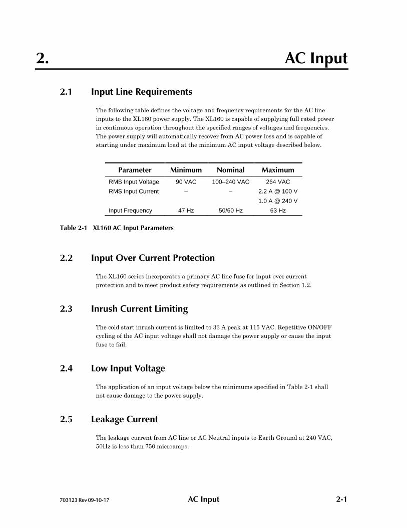
2.1 Input Line Requirements
The following table defines the voltage and frequency requirements for the AC line inputs to the XL160 power supply. The XL160 is capable of supplying full rated power in continuous operation throughout the specified ranges of voltages and frequencies. The power supply will automatically recover from AC power loss and is capable of starting under maximum load at the minimum AC input voltage described below.
Parameter Minimum Nominal Maximum
RMS Input Voltage 90 VAC 100–240 VAC 264 VAC RMS Input Current – – 2.2 A @ 100 V
1.0 A @ 240 V Input Frequency 47 Hz 50/60 Hz 63 Hz
Table 2-1 XL160 AC Input Parameters
2.2 Input Over Current Protection
The XL160 series incorporates a primary AC line fuse for input over current protection and to meet product safety requirements as outlined in Section 1.2.
2.3 Inrush Current Limiting
The cold start inrush current is limited to 33 A peak at 115 VAC. Repetitive ON/OFF cycling of the AC input voltage shall not damage the power supply or cause the input fuse to fail.
2.4 Low Input Voltage
The application of an input voltage below the minimums specified in Table 2-1 shall not cause damage to the power supply.
2.5 Leakage Current
The leakage current from AC line or AC Neutral inputs to Earth Ground at 240 VAC, 50Hz is less than 750 microamps.
703123 Rev 09-10-17 AC Input 2-1
3. DC Outputs
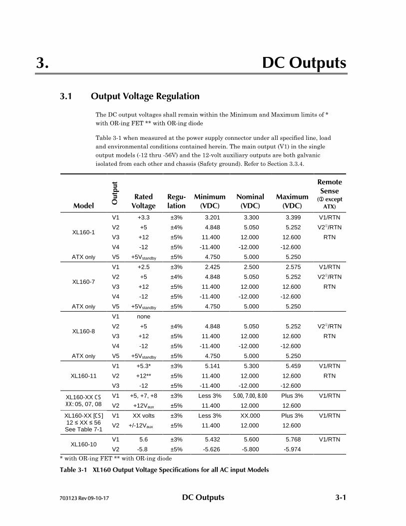
3.1 Output Voltage Regulation
The DC output voltages shall remain within the Minimum and Maximum limits of * with OR-ing FET ** with OR-ing diode
Table 3-1 when measured at the power supply connector under all specified line, load and environmental conditions contained herein. The main output (V1) in the single output models (-12 thru -56V) and the 12-volt auxiliary outputs are both galvanic isolated from each other and chassis (Safety ground). Refer to Section 3.3.4.
Model Out
put
Rated Voltage
Regu-lation
Minimum(VDC)
Nominal (VDC)
Maximum (VDC)
RemoteSense
( except ATX)
XL160-1
V1 +3.3 ±3% 3.201 3.300 3.399 V1/RTN V2 +5 ±4% 4.848 5.050 5.252 V2/RTN V3 +12 ±5% 11.400 12.000 12.600 RTN V4 -12 ±5% -11.400 -12.000 -12.600
ATX only V5 +5Vstandby ±5% 4.750 5.000 5.250
XL160-7
V1 +2.5 ±3% 2.425 2.500 2.575 V1/RTN V2 +5 ±4% 4.848 5.050 5.252 V2/RTN V3 +12 ±5% 11.400 12.000 12.600 RTN V4 -12 ±5% -11.400 -12.000 -12.600
ATX only V5 +5Vstandby ±5% 4.750 5.000 5.250
XL160-8
V1 none V2 +5 ±4% 4.848 5.050 5.252 V2/RTN V3 +12 ±5% 11.400 12.000 12.600 RTN V4 -12 ±5% -11.400 -12.000 -12.600
ATX only V5 +5Vstandby ±5% 4.750 5.000 5.250
XL160-11 V1 +5.3* ±3% 5.141 5.300 5.459 V1/RTN V2 +12** ±5% 11.400 12.000 12.600 RTN V3 -12 ±5% -11.400 -12.000 -12.600
XL160-XX CS XX: 05, 07, 08
V1 +5, +7, +8 ±3% Less 3% 5.00, 7.00, 8.00 Plus 3% V1/RTN V2 +12Vaux ±5% 11.400 12.000 12.600
XL160-XX [CS] 12 ≤ XX ≤ 56 See Table 7-1
V1 XX volts ±3% Less 3% XX.000 Plus 3% V1/RTN V2 +/-12Vaux ±5% 11.400 12.000 12.600
XL160-10 V1 5.6 ±3% 5.432 5.600 5.768 V1/RTN V2 -5.8 ±5% -5.626 -5.800 -5.974
* with OR-ing FET ** with OR-ing diode
Table 3-1 XL160 Output Voltage Specifications for all AC input Models
703123 Rev 09-10-17 DC Outputs 3-1
XL160 Series Product Specification
3.2 No Load Operation
The power supply will operate with reduced output voltage regulation of +/-10% with all outputs unloaded. This no load condition will not damage the XL160 or cause a hazardous condition, however the Power Good signal may not go true with less than a 5-watt load. The power supply will remain stable and operate normally after application of loads.
CAUTION
Remove AC power prior to installing or removing secondary loads.
3.3 Output Current/Power
The maximum available output power is always a function of the cooling airflow and temperature. The total output is reduced with unrestricted natural convection cooling and an ambient temperature of 50°C or less (see Sections 3.3.1 and 3.3.2). No output will exceed 240VA under any of overload or short circuit condition including single component fault conditions as described by IEC 60950.
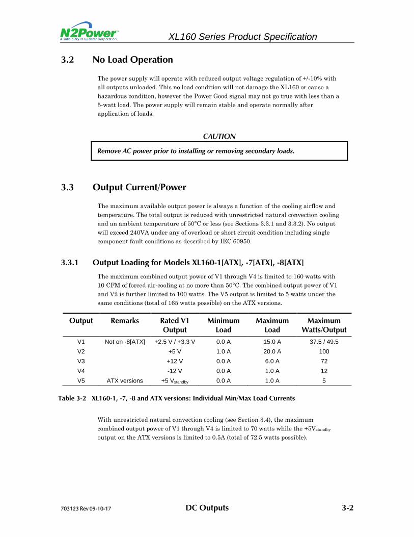
3.3.1 Output Loading for Models XL160-1[ATX], -7[ATX], -8[ATX]
The maximum combined output power of V1 through V4 is limited to 160 watts with 10 CFM of forced air-cooling at no more than 50°C. The combined output power of V1 and V2 is further limited to 100 watts. The V5 output is limited to 5 watts under the same conditions (total of 165 watts possible) on the ATX versions.
Output Remarks Rated V1 Output
Minimum Load
Maximum Load
Maximum Watts/Output
V1 Not on -8[ATX] +2.5 V / +3.3 V 0.0 A 15.0 A 37.5 / 49.5 V2 +5 V 1.0 A 20.0 A 100 V3 +12 V 0.0 A 6.0 A 72 V4 -12 V 0.0 A 1.0 A 12 V5 ATX versions +5 Vstandby 0.0 A 1.0 A 5
Table 3-2 XL160-1, -7, -8 and ATX versions: Individual Min/Max Load Currents
With unrestricted natural convection cooling (see Section 3.4), the maximum combined output power of V1 through V4 is limited to 70 watts while the +5Vstandby output on the ATX versions is limited to 0.5A (total of 72.5 watts possible).
703123 Rev 09-10-17 DC Outputs 3-2

XL160 Series Product Specification
3.3.2 Output Loading for Models XL160-11
The maximum combined output power of V1 through V3 is limited to 160 watts with 10 CFM of forced air-cooling at no more than 50°C.
Output Rated V1 Output
Minimum Load
Maximum Load
Maximum Watts/Output
V1 +5 V 1.0 A 20.0 A 100 V2 +12 V 0.0 A 6.0 A 72 V3 -12 V 0.0 A 1.0 A 12
Table 3-3 XL160-11 Individual Min/Max Load Currents
With unrestricted natural convection cooling (see Section 3.4), the maximum combined output power of V1 through V3 is limited to 70 watts.
3.3.3 Output Loading for Models XL160-10
The maximum combined output power of V1 and V2 is limited to 143 watts with 10 CFM of forced air-cooling at no more than 50°C. This is an exception to the 160-watt output of the other models in this specification.
Output Rated V1 Output
Minimum Load
Maximum Load
Maximum Watts/Output
V1 +5.6 V 0.9 A 24.0 A 134 V2 -5.8 V 0.0 A 1.5 A 8.7
Table 3-4 XL160-10 Individual Min/Max Load Currents
With unrestricted natural convection cooling (see Section 3.4), the maximum combined output power of V1 through V3 is limited to 70 watts.
3.3.4 Output Loading for Models XL160-05 [CS] through XL160-56 [CS]
The output currents listed in this section require 10 CFM of forced air-cooling at no more than 50°C. The total output of 160-watts is reduced to 115-watts with unrestricted natural convection cooling (see Section 3.4) except for the XL160-05 thru XL160-08, which are reduced to 70-watts.
These single-output models (XL160-XX [CS] where [CS] means with or without current sharing) all have an auxiliary 12V output (V2, 12V AUX) that is typically used to drive a cooling fan. The load on this V2 output can vary from 0 to 1.0 amps and does not affect the Power Good or PS_OK signals. Its load power detracts from the 160-watts otherwise available to the V1 load. On the XL160-05 thru XL160-08 models, the negative side of the V2 output is connected to the common ground “DC RETURN”. The main output (V1) in the single output models (-12 thru -56V) and the 12-volt auxiliary outputs are both galvanic isolated from each other and chassis (Safety ground). Thus, they can be used as either a positive or negative supply.
703123 Rev 09-10-17 DC Outputs 3-3

XL160 Series Product Specification
The signals on J3: DC Return, Current Share, PG and PS_OK are all reference to the negative rail of the V1 Main output. Connecting the “+” voltage lead to ground or customer’s return will yield a negative voltage on the “-“ leads.
Model Rated V1 Output
Minimum Power
Good Load (5W)
Maximum Continuous
Load XL160-05 [CS] 5 V 1.00 A 32.0 A XL160-07 [CS] 7 V 0.72 A 22.8 A XL160-08 [CS] 8 V 0.63 A 20.0 A XL160-12 [CS] 12 V 0.40 A 13.3 A XL160-15 [CS] 15 V 0.33 A 10.7 A XL160-19 [CS] 19 V 0.26 A 8.42 A XL160-24 [CS] 24 V 0.20 A 6.67 A XL160-28 [CS] 28 V 0.18 A 5.71 A XL160-30 [CS] 30 V 0.17 A 5.33 A XL160-33 [CS] 33 V 0.15 A 4.84 A XL160-48 [CS] 48 V 0.11 A 3.33 A XL160-51 [CS] 51 V 0.10 A 3.14 A XL160-54 [CS] 54 V 0.09 A 2.96 A XL160-56 [CS] 56 V 0.09 A 2.86 A
Minimum load needed for the Power Good signal to go true (high) and the PS_OK signal to go low
Assuming no load on V2 output & that cooling requirements are met
Table 3-5 Min/Max Load Currents XL160-05 [CS] thru XL160-56 [CS]
3.4 Cooling
The power supply can be used under certain output loading conditions in natural convection cooling or with forced air-cooling. The XL160 may be mounted in any attitude.
3.4.1 Unrestricted Convection Cooling
The maximum continuous output rating of all DC outputs combined is reduced under natural convection cooling with a maximum ambient temperature of 50°C (see Sections 3.3.1 through 3.3.4). On the XL160-1[ATX], -7[ATX] models, the sum of the V1 and V2 outputs must not exceed 40-watts. On the XL160-8[ATX] models, the V2 output must not exceed 40-watts.
703123 Rev 09-10-17 DC Outputs 3-4
XL160 Series Product Specification
3.4.2 Forced Air Cooling
The maximum continuous rating of all DC outputs combined is 160-watts with a minimum of 10 CFM of forced-air cooling at a maximum of 50°C. On the XL160-1[ATX], -7[ATX] models, the sum of the V1 and V2 outputs must not exceed 100-watts. On the XL160-8[ATX] models, the V2 output must not exceed 100-watts. Airflow must be in the same plane as the circuit board (impinging on any side of the XL160).
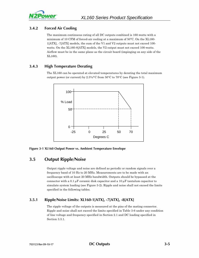
3.4.3 High Temperature Derating
The XL160 can be operated at elevated temperatures by derating the total maximum output power (or current) by 2.5%/°C from 50°C to 70°C (see Figure 3-1).
-25 0 25 50 70 Degrees C
0
50
100
% Load
Figure 3-1 XL160 Output Power vs. Ambient Temperature Envelope
3.5 Output Ripple/Noise
Output ripple voltage and noise are defined as periodic or random signals over a frequency band of 10 Hz to 20 MHz. Measurements are to be made with an oscilloscope with at least 20 MHz bandwidth. Outputs should be bypassed at the connector with a 0.1 µF ceramic disk capacitor and a 10 µF tantalum capacitor to simulate system loading (see Figure 3-2). Ripple and noise shall not exceed the limits specified in the following tables.
3.5.1 Ripple/Noise Limits: XL160-1[ATX], -7[ATX], -8[ATX]
The ripple voltage of the outputs is measured at the pins of the mating connector. Ripple and noise shall not exceed the limits specified in Table 3-6 under any condition of line voltage and frequency specified in Section 2.1 and DC loading specified in Section 3.3.1.
703123 Rev 09-10-17 DC Outputs 3-5
XL160 Series Product Specification
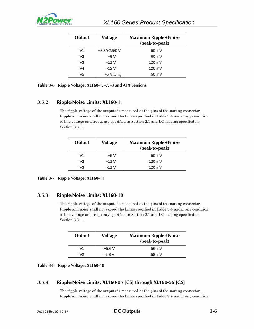
Output Voltage Maximum Ripple+Noise (peak-to-peak)
V1 +3.3/+2.5/0 V 50 mV V2 +5 V 50 mV V3 +12 V 120 mV V4 -12 V 120 mV V5 +5 Vstandby 50 mV
Table 3-6 Ripple Voltage: XL160-1, -7, -8 and ATX versions
3.5.2 Ripple/Noise Limits: XL160-11
The ripple voltage of the outputs is measured at the pins of the mating connector. Ripple and noise shall not exceed the limits specified in Table 3-6 under any condition of line voltage and frequency specified in Section 2.1 and DC loading specified in Section 3.3.1.
Output Voltage Maximum Ripple+Noise (peak-to-peak)
V1 +5 V 50 mV V2 +12 V 120 mV V3 -12 V 120 mV
Table 3-7 Ripple Voltage: XL160-11
3.5.3 Ripple/Noise Limits: XL160-10
The ripple voltage of the outputs is measured at the pins of the mating connector. Ripple and noise shall not exceed the limits specified in Table 3-6 under any condition of line voltage and frequency specified in Section 2.1 and DC loading specified in Section 3.3.1.
Output Voltage Maximum Ripple+Noise (peak-to-peak)
V1 +5.6 V 56 mV V2 -5.8 V 58 mV
Table 3-8 Ripple Voltage: XL160-10
3.5.4 Ripple/Noise Limits: XL160-05 [CS] through XL160-56 [CS]
The ripple voltage of the outputs is measured at the pins of the mating connector. Ripple and noise shall not exceed the limits specified in Table 3-9 under any condition
703123 Rev 09-10-17 DC Outputs 3-6

XL160 Series Product Specification
of line voltage and frequency specified in Section 2.1 and DC loading specified in Section 3.3.2.
Model Rated V1 Output
Maximum Ripple+Noise (peak-to-peak)
XL160-05 [CS] 5 V 50 mV XL160-07 [CS] 7 V 70 mV XL160-08 [CS] 8 V 80 mV XL160-12 [CS] 12 V 120 mV XL160-15 [CS] 15 V 150 mV XL160-19 [CS] 19 V 190 mV XL160-24 [CS] 24 V 240 mV XL160-28 [CS] 28 V 280 mV XL160-30 [CS] 30 V 300 mV XL160-33 [CS] 33 V 330 mV XL160-48 [CS] 48 V 480 mV XL160-51 [CS] 51 V 510 mV XL160-54 [CS] 54 V 540 mV XL160-56 [CS] 56 V 560 mV All of the above V2 (12V) 120 mV
Table 3-9 Ripple Voltage: XL160-05 [CS] thru XL160-56 [CS]
3.5.5 Ripple/Noise Test Setup Power Supply
AC Line
AC Neutral
V Out
DC Return Earth Ground
Load Load must be isolated from the earth ground of the power supply.
Differential Oscilloscope
10uf 0.1uf
Notes:
1. Load the output with its minimalload current.
2. Connect the probes as shown butkeep them as close as possible tothe J2 (output) connector.
3. Repeat the measurement withmaximum load on the output.
Figure 3-2 Ripple Noise Measurement Setup
703123 Rev 09-10-17 DC Outputs 3-7
XL160 Series Product Specification
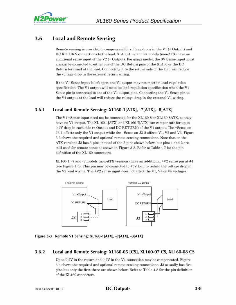
3.6 Local and Remote Sensing
Remote sensing is provided to compensate for voltage drops in the V1 (+ Output) and DC RETURN connections to the load. XL160-1, -7 and -8 models (non-ATX) have an additional sense input of the V2 (+ Output). For every model, the 0V Sense input must always be connected to either one of the DC Return pins of the XL160 or the DC Return terminal at the load. Connecting it to the return side of the load will reduce the voltage drop in the external return wiring.
If the V1 Sense input is left open, the V1 output may not meet its load regulation specification. The V1 output will meet its load regulation specification when the V1 Sense pin is connected to one of the V1 output pins. Connecting the V1 Sense pin to the V1 output at the load will reduce the voltage drop in the external V1 wiring.
3.6.1 Local and Remote Sensing: XL160-1[ATX], -7[ATX], -8[ATX]
The V1 +Sense input need not be connected for the XL160-8 or XL160-8ATX, as they have no V1 output. The XL160-1[ATX] and XL160-7[ATX] can compensate for up to 0.2V drop in each side (+ Output and DC RETURN) of the V1 output. The +Sense on J3-1 affects only the V1 output while the –Sense on J3-2 affects V1, V2 and V3. Figure 3-3 shows the required and optional remote sensing connections. Note that on the ATX versions J3 has 5-pins instead of the 3-pins shown below, but pins 1 and 2 are still used for remote sense as shown in Figure 3-3. Refer to Table 4-7 for the pin definition of the XL160 connectors.
XL160-1, -7 and -8 models (non-ATX versions) have an additional +V2 sense pin at J4 (see Figure 4-3). This pin may be connected to +5V load to reduce the voltage drop in the V2 load wiring. The +V2 sense input does not affect the V1, V4 or V5 voltages.
Local V1 Sense
Load V1 +Output
DC RETURN
123
J3 1 23J3
Remote V1 Sense
V1 +Output
DC RETURN Load
Figure 3-3 Remote V1 Sensing: XL160-1[ATX], -7[ATX], -8[ATX]
3.6.2 Local and Remote Sensing: XL160-05 [CS], XL160-07 CS, XL160-08 CS
Up to 0.2V in the return and 0.2V in the V1 connection may be compensated. Figure 3-4 shows the required and optional remote sensing connections. J3 actually has five pins but only the first three are shown below. Refer to Table 4-8 for the pin definition of the XL160 connectors.
703123 Rev 09-10-17 DC Outputs 3-8

XL160 Series Product Specification
This model contains an internal OR-ing diode so that V1 output of multiple power supplies may be connected in parallel. Follow the same sense wiring for each paralleled supply as if it were a single supply.
Local V1 Sense
Load V1 +Output
DC RETURN
123
J3 123J3
Remote V1 Sense
V1 +Output
DC RETURN Load
Figure 3-4 Remote Sensing Wiring: XL160-05 [CS], -07 CS and -08 CS
3.6.3 Local and Remote Sensing: XL160-10
Up to 0.2V in the return and 0.2V in the V1 connection may be compensated. The + and – sense inputs are found on J3 and affect only the V1 output.
3.6.4 Local and Remote Sensing: XL160-11
Up to 0.2V in the return and 0.2V in the V1 connection may be compensated. The +Sense input is found on the single-pin header J4 (see Figure 4-3). The –Sense input is found on J3-1. Both sense inputs affect the V1 and V2 outputs but not V3.
3.6.5 Local and Remote Sensing: XL160-12 [CS] through XL160-56 [CS]
Up to 0.5V in the return and 0.5V in the V1 connection may be compensated. Figure 3-5 shows the required and optional remote sensing connections. J3 actually has five pins but only the first three are shown below. Refer to Figure 4-3 for the pin definition of the XL160 connectors. These models contain internal OR-ing diodes so that V1 output of multiple power supplies may be connected in parallel. Follow the same sense wiring for each paralleled supply as if it were a single supply.
Local V1 Sense
Load V1 +Output
DC RETURN
123
J3 123J3
Remote V1 Sense
V1 +Output
DC RETURN Load
Figure 3-5 Remote Sensing Wiring: XL160-12 [CS] through XL160-56 [CS]
703123 Rev 09-10-17 DC Outputs 3-9

XL160 Series Product Specification
3.7 Parallel Operation
3.7.1 XL160-05 CS, -07 CS, -08 CS and XL160-12 CS through -56 CS
The V1 output of two, three or four XL160-xx CS power supplies may be connected directly in parallel to provide higher output power. They can also be used in an N+1 configuration to provide higher output power and greater reliability. Each of these models has a built-in V1 output OR-ing diode (or MOSFET) and a Current Share signal for active load-leveling parallel operation.
The V2 outputs must not be connected together and they are unaffected by the active current sharing of the V1 outputs.
3.7.2 Current Sharing Connections
The Current Share signal (see Table 4-7) of each supply operating in parallel must be connected together. Power sharing does not require the 0V Sense signals be connected together, but the sharing accuracy may not meet published specification unless they are also connected together.
Power Good signals may be wire OR-ed together, but this is not recommended, as a failing power supply will pull the signal low. They should be monitored individually by the user’s system.
3.7.3 Current Share Accuracy
When all the current share signals are connected together and all the 0V Sense signals are connected together, the load delivered by any two supplies of the sharing supplies will not vary by more than 10% at full load.
3.7.4 Transients
The output rise time and monotonic requirements of Section 6.1may not be met where the load exceeds 160 watts, because of the difference in start-up times of the paralleled power supplies.
When the AC line to one of the parallel power supplies is disconnected or reconnected, or a power supply fails, the transient on the V1 output is within five (5) percent of nominal output voltage, although the output voltage may ramp to a new nominal voltage within the regulation band.
3.7.5 XL160-11
The XL160-11 has an output OR-ing FET on V1 and an OR-ing diode on the V2 output. For redundancy purposes, these outputs may be connected in parallel with those of identical supplies. However, the total output power available is still the same as a single supply. Multiple V3 outputs may not be connected together.
703123 Rev 09-10-17 DC Outputs 3-10
XL160 Series Product Specification
3.8 Output Protection
There are three different output protection schemes designed to protect the load and the XL160 from component failures and extraordinary circumstances.
3.8.1 Over Temperature Protection
If the XL160 is operated without adequate cooling, it will sense an over-temperature condition and shut itself down. It will not restart until it has cooled down to below its maximum operating temperature and the AC power is turned off and back on.
3.8.2 V2 or V3 Outputs Over-Load Protection
The V2 outputs of the XL160-05, 07, -08, and -12 through -56 are current limited at approximately 1.5A through a thermally protected linear regulator. The same is true for the V3 output on the XL160-11. The V2 output (-5.8V) of the XL160-10 is current limited at approximately 2A through a thermally protected linear regulator.
An overload on the V2 output (V3 on the XL160-11) should not affect the operation of the other outputs unless the V2 output power adds to already excessive output power, thereby causing over-power protection. The V2 output will resume normal operation when the over-load condition is removed.
3.8.3 Over-Power Protection
Total output power in excess of approximately 190-watts will cause the XL160 to shut down all outputs except for the V5 (+5Vstandby) output on ATX models. The power supply will periodically attempt to restart until the over-load condition is removed.
Pulsating loads of 150% of the rated output can be sustained for 10-milliseconds provided the duty cycle does not exceed 10%. The total RMS power must still be limited to 160-watts.
3.8.4 Over Voltage Protection
No single fault is able to cause a sustained over voltage condition on any output. The following outputs have OVP sensing and will shut the supply down if the output reaches the OVP threshold. Following an OVP event, the XL160 will not restart until AC power is turned off and back on.
Model OVP Sensing on Outputs:
XL160-1,-7[ATX] V1, V2, V3 XL160-8[ATX] V2, V3 XL160-11 V1, V2 XL160-10 V1 XL160-XX [CS] V1
Table 3-10 OVP Protected Outputs by Model
703123 Rev 09-10-17 DC Outputs 3-11

XL160 Series Product Specification
The XL160 will shut down under the following over voltage conditions:
Rated Output Voltage
Minimum OVP
Threshold
Nominal OVP
Threshold
Maximum OVP
Threshold
2.5 V 2.87 V 3.15 V 3.44 V 3.3 V 3.76 V 4.2 V 4.9 V 5.0 V 5.74 V 6.3 V 6.88 V 5.6 V 6.30 V 7.0 V 7.70 V 7 V 7.88 V 8.7 V 9.63 V 8 V 9.00 V 10.0 V 11.0 V
12 V 13.5 V 15.0 V 16.5 V 15 V 16.9 V 18.8 V 20.6 V 19 V 21.4 V 23.8 V 26.1 V 24 V 27.0 V 30.0 V 33.0 V 28 V 31.5 V 35.0 V 33.5 V 30 V 33.8 V 37.5 V 41.3 V 33 V 37.1 V 41.3 V 45.4 V 48 V 54.0 V 58.0 V 66.0 V 51 V 57.4 V 63.8 V 70.1 V 54 V 60.8 V 64.8 V 74.3 V 56 V 63.0 V 70.0 V 77.0 V
Table 3-11 Over Voltage Protection Limits by Rated Output Voltage
3.9 Output Rise Time
All output voltages shall rise from 10% to 90% of nominal output voltage (as specified in * with OR-ing FET ** with OR-ing diode
Table 3-1) within 0.2ms to 20ms. The output voltages waveform must be a monotonic ramp from 10% to 90% of final setpoint within the regulation band under any loading conditions specified in the respective load current tables in Section 6.
For the purposes of this specification, a monotonic ramp is defined as always having a positive slope of from zero to 10*Vout volts/millisecond. During any 5-millisecond portion of the ramp, its slope must greater than 5% of its rated voltage per millisecond.
3.10 Overshoot At Turn On/Turn Off
The output voltage overshoot upon the application or removal of the input mains voltage is less than 10% above the nominal voltage. No opposite polarity voltage is present on any output during turn on or turn off.
703123 Rev 09-10-17 DC Outputs 3-12

XL160 Series Product Specification
3.11 Output Transients
The maximum output voltage transient caused by step load changes will not exceed the output voltage regulation limits by more than 5%. With an AC input as specified in Section 2.1, the power supply will remain stable when subjected to the load transients described below:
• Load changes between 75% and 100% on any output
• Load changing repetition of 50 to 333 cycles per second
• Transient load slew rate = 1.0 A/microsecond
• Capacitive loading per Table 3-12
3.12 Closed Loop Stability
The power supply is unconditionally stable under all line/load/transient load conditions including the capacitive loads specified in Table 3-12. The power supply shall exhibit a minimum of 45-degrees phase margin and 6 dB gain margin.
3.13 Capacitive Loading
The power supply will power up and operate normally with the capacitances listed in Table 3-12 simultaneously present on the outputs.
XL160-:
-1[ATX], -7[ATX], -8[ATX]
-05 thru -11 -12
-15 thru -19
-24 thru -33
-48 thru -56
Output: have demonstrated starting and stability with the following capacitive loads +3.3 V / +2.5 V 6,000 μF +5 V 10,000 μF +5 Vstandby (ATX) 100 μF +12 V 1,000 μF V1 (Main Output) 10,000 μF 4,000 μF 3,000 μF 2,000 μF 500 μF 12 Vaux 350 μF 350 μF 350 μF 350 μF 350 μF 350 μF
Table 3-12 XL160 Demonstrated Capacitive Loading
703123 Rev 09-10-17 DC Outputs 3-13

4. General Specifications
4.1 Environmental
The XL160 meets or exceeds the following environmental specifications:
Parameter Conditions Specification Remarks Temperature Operating -25°C to 50°C See cooling requirements
Non-Operating -40°C to 85°C Relative Humidity Operating 95% Maximum Non-Condensing
Non-Operating 95% Maximum Non-Condensing Altitude Operating 6,561 feet MSL Max. 2,000 meters
Non-Operating 50,000 feet MSL Max. 15,240 meters Vibration No damage 2.4G RMS Maximum 5-500Hz, 10-min. each axis per
MIL-PRF-28800F: 3.8.4.1 (Class 3,4) 6.0G RMS Maximum 100-1,000Hz random, 10-min.
vertical axis only Mechanical Shock No damage 30G half-sine, 11mS Six shocks each axis per
MIL-PRF-28800F: 4.5.5.4.1
Table 4-1 Environmental Specifications
4.2 Mean Time Between Failures
The calculated MTBF of XL160-1, 7 and 8 models is equal to or greater than 525,000 hours of continuous operation at maximum output loading and worst case input line voltage with forced-air cooling at 25°C. The ATX versions of XL160-1, 7 and 8 are rated at 430,000 hours. The XL160-12 thru 56 CS models are rated at 675,000 hours. N2Power does not warrant the MTBF to be representative of any particular unit. The MTBF of the power supply is calculated with an 80% confidence level in accordance with Bellcore, SR-332, Issue 2. Actual failure rates vary from unit to unit.
4.3 Component Stress
The XL160 design followed these component-derating guidelines: semiconductor junction temperatures shall not exceed ninety (90) percent of manufacturer’s rating with an ambient of 50°C. Inductor winding temperatures shall not exceed safety agency requirements. Capacitor case temperatures shall not exceed 95% of rated temperature. Resistor power dissipation derating is greater than 30%. Component voltage and current derating is greater than 10% at 50°C.
703123 Rev 09-10-17 General Specifications 4-1

XL160 Series Product Specification
4.4 Labeling/Marking
The power supply is marked and labeled with the N2Power logo and part number, model number, input and output specifications, production code, appropriate safety agency logos, CE mark, patent number, and country of origin. A typical label is pictured below.
Figure 4-1 Sample XL160 Label
4.5 Weight
Model Pounds Ounces Kilograms XL160-1ATX, -7ATX 0.70 11.2 0.32 XL160-8ATX 0.66 10.6 0.30 XL160-1, -7 0.68 10.9 0.31 XL160-8 0.64 10.3 0.29 XL160-10 0.66 10.6 0.30 XL160-11 0.65 10.4 0.30 XL160-05 [CS], -07 CS, -08 CS 0.63 10.1 0.29 XL160-12 [CS] thru -56 [CS] 0.59 9.5 0.27
Table 4-2 XL160 Weights
4.6 Mounting
The XL160 may be mounted in any attitude but must be mounted on all four corners. No. 6 or M3 mounting hardware should not exceed .282-inches (7.16-mm) in diameter for any lock washer, flat washer, standoff, screw head or other mounting hardware to avoid contact and maintain adequate safety agency spacing requirements with components or printed circuit board traces.
703123 Rev 09-10-17 General Specifications 4-2
XL160 Series Product Specification
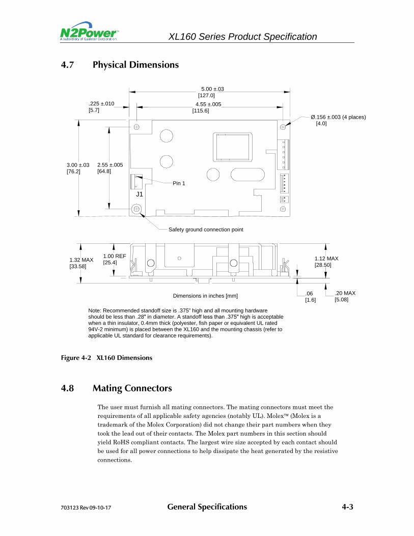
4.7 Physical Dimensions
Figure 4-2 XL160 Dimensions
4.8 Mating Connectors
The user must furnish all mating connectors. The mating connectors must meet the requirements of all applicable safety agencies (notably UL). Molex (Molex is a trademark of the Molex Corporation) did not change their part numbers when they took the lead out of their contacts. The Molex part numbers in this section should yield RoHS compliant contacts. The largest wire size accepted by each contact should be used for all power connections to help dissipate the heat generated by the resistive connections.
Safety ground connection point
Pin 1
4.55 ±.005 [115.6]
5.00 ±.03 [127.0]
Ø.156 ±.003 (4 places) [4.0]
J1
.225 ±.010 [5.7]
2.55 ±.005 [64.8]
3.00 ±.03 [76.2]
1.00 REF [25.4] 1.32 MAX
[33.58] 1.12 MAX [28.50]
.20 MAX [5.08]
.06 [1.6] Dimensions in inches [mm]
Note: Recommended standoff size is .375” high and all mounting hardware should be less than .28" in diameter. A standoff less than .375" high is acceptable when a thin insulator, 0.4mm thick (polyester, fish paper or equivalent UL rated 94V-2 minimum) is placed between the XL160 and the mounting chassis (refer to applicable UL standard for clearance requirements).
703123 Rev 09-10-17 General Specifications 4-3

XL160 Series Product Specification
Note that the female contacts that mate to the power supply are only rated for 25-30 mating cycles. Excessive mating cycles causes dramatically increased terminal resistance and heating resulting in the eventual failure of the mating terminal and possibly the header on the power supply.
CAUTION
The pin-1 location differs amongst connector manufacturers. Sometimes pin-1 differs between the header (on the power supply) and the mating housing from the same manufacturer. Disregard the manufacturer’s pin-1 location and follow only the pin-1 locations in Figure 4-3.
4.8.1 AC Input Mating Connector (J1)
The AC input connector to the XL160 is a 3-pin Molex (Molex is a trademark of the Molex Corporation) KK style header with 0.156” centers. The center pin is omitted to provide adequate insulation spacing. The Molex part numbers for the mating housing and crimp-style snap-in terminals are listed below. There may be equivalent connectors available from other manufacturers. The line side of the input should be connected to the pin closest to the mounting hole (see Figure 4-2).
J1 Molex P/N
Connector Circuits (pins) 2 of 3 Mating Housing 09-50-8031 Rated Contact Current 7.0 A Crimp Terminal (tin) 08-50-0106 Rated Wire Size AWG 18 or 20
Table 4-3 J1 Mating Connector
703123 Rev 09-10-17 General Specifications 4-4
XL160 Series Product Specification
4.8.2 DC Output Connector (J2)
Except for the XL160-2, the DC output connector is a Molex KK style header with 0.156” centers. The Molex part numbers for the mating housing and crimp-style snap-in terminals are listed below. There may be equivalent connectors available from other manufacturers.
J2
XL160-1[ATX], -7[ATX], -8[ATX],
XL160-11 XL160-05 [CS],
-07 CS, -08 CS, -10 XL160-xx [CS] Connector Circuits (pins) 14 6 6 Mating Housing 09-50-8141 Stripped and tinned wire 09-50-8061 Crimp Terminal (tin) 08-52-0071 N/A 08-50-0106 Rated Wire Size AWG 18 or 20 AWG 12 max. AWG 18 or 20
Table 4-4 J2 Mating Connectors
4.8.3 Remote Sense / PG Connector (J3)
The Remote Sense/PG connector on the XL160 is a Molex KK style header with 0.100” centers. The Molex part numbers for the mating housing and crimp-style snap-in terminals are listed below. There may be equivalent connectors available from other manufacturers.
J3 XL160-1, -7, -8
XL160-11*
XL160-1ATX, -7ATX, -8ATX, XL160-05 [CS], -07 CS, -08 CS
XL160-10 XL160-xx [CS] Connector Circuits (pins) 3 5 6 Mating Housing 22-01-3037 22-01-3057 22-01-3067 Crimp Terminal (tin, 2.5A) 08-52-0123 08-52-0123 08-52-0123 Rated Wire Size AWG 22 to 30 AWG 22 to 30 AWG 22 to 30 * For XL160-1, 7, 8 and 11 models only, it is recommended to use the Molex 22-01-
3037 housing and not an equivalent from another manufacturer.
Table 4-5 J3 Mating Connectors
703123 Rev 09-10-17 General Specifications 4-5

XL160 Series Product Specification
4.8.4 J4 Connector: 12V Aux or V2 Sense (see Table 4-7 & Table 4-8)
The 12V AUX or V2 Sense connector (see Table 4-6) is a 2-pin header with 0.100” centers. The part numbers for the mating housing and crimp-style snap-in terminals are listed below. There may be equivalent connectors available from other manufacturers.
J4 on the XL160-1,7,8 models is a single pin header for remote sensing the V2 (+5V) output. Remote sensing will help eliminate the voltage drop in the wires from the XL160-1,7,8 to the load. This pin should be connected to the +5V output at the load, not J2.
J4
XL160-05 [CS], -07 CS, -08 CS XL160-xx [CS]
XL160-10
XL160-11 XL160-1, -7, -8
(not ATX)
Connector Circuits (pins) 2 1 Mating Housing Molex P/N 22-01-3027 Molex P/N 22-01-2011
or TE Connectivity Ltd P/N 7-87499-2 Crimp Terminal (tin, 2.5A) Molex 08-52-0123 Molex 08-52-0123
or TE Connectivity Ltd P/N 6-87756-6 Rated Wire Size AWG 22 to 30 AWG 22 to 30
Table 4-6 J4 Mating Connectors
4.9 Output Grounding
The DC RETURN signal may be connected to the power supply chassis ground (safety ground) at the plated through mounting hole near the input connector.
703123 Rev 09-10-17 General Specifications 4-6
XL160 Series Product Specification
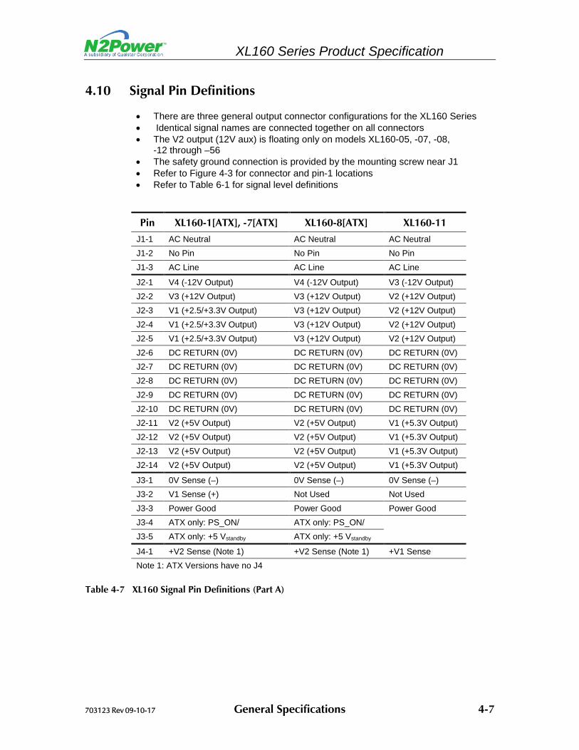
4.10 Signal Pin Definitions
• There are three general output connector configurations for the XL160 Series• Identical signal names are connected together on all connectors• The V2 output (12V aux) is floating only on models XL160-05, -07, -08,
-12 through –56• The safety ground connection is provided by the mounting screw near J1• Refer to Figure 4-3 for connector and pin-1 locations• Refer to Table 6-1 for signal level definitions
Pin XL160-1[ATX], -7[ATX] XL160-8[ATX] XL160-11 J1-1 AC Neutral AC Neutral AC Neutral J1-2 No Pin No Pin No Pin J1-3 AC Line AC Line AC Line
J2-1 V4 (-12V Output) V4 (-12V Output) V3 (-12V Output) J2-2 V3 (+12V Output) V3 (+12V Output) V2 (+12V Output) J2-3 V1 (+2.5/+3.3V Output) V3 (+12V Output) V2 (+12V Output) J2-4 V1 (+2.5/+3.3V Output) V3 (+12V Output) V2 (+12V Output) J2-5 V1 (+2.5/+3.3V Output) V3 (+12V Output) V2 (+12V Output) J2-6 DC RETURN (0V) DC RETURN (0V) DC RETURN (0V) J2-7 DC RETURN (0V) DC RETURN (0V) DC RETURN (0V) J2-8 DC RETURN (0V) DC RETURN (0V) DC RETURN (0V) J2-9 DC RETURN (0V) DC RETURN (0V) DC RETURN (0V) J2-10 DC RETURN (0V) DC RETURN (0V) DC RETURN (0V) J2-11 V2 (+5V Output) V2 (+5V Output) V1 (+5.3V Output) J2-12 V2 (+5V Output) V2 (+5V Output) V1 (+5.3V Output) J2-13 V2 (+5V Output) V2 (+5V Output) V1 (+5.3V Output) J2-14 V2 (+5V Output) V2 (+5V Output) V1 (+5.3V Output)
J3-1 0V Sense (–) 0V Sense (–) 0V Sense (–) J3-2 V1 Sense (+) Not Used Not Used J3-3 Power Good Power Good Power Good J3-4 ATX only: PS_ON/ ATX only: PS_ON/ J3-5 ATX only: +5 Vstandby ATX only: +5 Vstandby
J4-1 +V2 Sense (Note 1) +V2 Sense (Note 1) +V1 Sense Note 1: ATX Versions have no J4
Table 4-7 XL160 Signal Pin Definitions (Part A)
703123 Rev 09-10-17 General Specifications 4-7
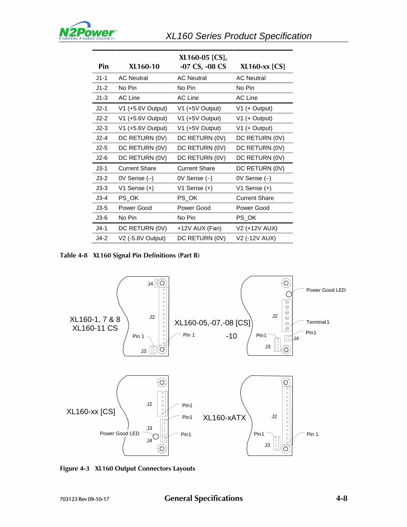
XL160 Series Product Specification
Pin XL160-10 XL160-05 [CS], -07 CS, -08 CS XL160-xx [CS]
J1-1 AC Neutral AC Neutral AC Neutral J1-2 No Pin No Pin No Pin J1-3 AC Line AC Line AC Line
J2-1 V1 (+5.6V Output) V1 (+5V Output) V1 (+ Output) J2-2 V1 (+5.6V Output) V1 (+5V Output) V1 (+ Output) J2-3 V1 (+5.6V Output) V1 (+5V Output) V1 (+ Output) J2-4 DC RETURN (0V) DC RETURN (0V) DC RETURN (0V) J2-5 DC RETURN (0V) DC RETURN (0V) DC RETURN (0V) J2-6 DC RETURN (0V) DC RETURN (0V) DC RETURN (0V)
J3-1 Current Share Current Share DC RETURN (0V) J3-2 0V Sense (–) 0V Sense (–) 0V Sense (–) J3-3 V1 Sense (+) V1 Sense (+) V1 Sense (+) J3-4 PS_OK PS_OK Current Share J3-5 Power Good Power Good Power Good J3-6 No Pin No Pin PS_OK
J4-1 DC RETURN (0V) +12V AUX (Fan) V2 (+12V AUX) J4-2 V2 (-5.8V Output) DC RETURN (0V) V2 (-12V AUX)
Table 4-8 XL160 Signal Pin Definitions (Part B)
Pin 1
Pin 1
J 2
J 3 J 4
Pin 1
Pin 1 Pin 1
J 2
J 3
Pin 1
J 2
J 3 J 4
Terminal 1
Power Good LED
Power Good LED Pin 1
J 2
J 3
Pin 1
Pin 1
J 4
XL160-1, 7 & 8 XL160-11 CS
XL160-05,-07,-08 [CS]
XL160-xATX XL160-xx [CS]
-10
Figure 4-3 XL160 Output Connectors Layouts
703123 Rev 09-10-17 General Specifications 4-8

5. Efficiency The power supply will meet high efficiencies under defined loading conditions specified in Table 5-1 with a line voltage of 230VAC and 10 CFM of cooling air at 25°C. Efficiency curves are shown in the following diagrams. These charts are for Current Sharing (CS) models, removing the Or-ing diodes will increase the efficiency by approximately 2%. This is available as an option.
XL160: -1[ATX] -05 [CS]
-12 [CS]
-15 [CS]
-24 [CS]
-48 [CS]
-7 -8
Efficiency 84% 83% 84% 85% 87% 88% 84% 84%
V1 3.8 A 25.6 A 10.6 A 8.5 A 5.3 A 2.7 A 5.0 A - V2 8.0 A 0.0 A 0.0 A 0.0 A 0.0 A 0.0 A 8.0 A 10.5 A V3 6.0 A - - - - - 6.0 A 6.0 A V4 0.3 A - - - - - 0.3 A 0.3 A V5 0.3 A (-1ATX)
Table 5-1 XL160 Output Currents at Rated Efficiency
XL160-15 [CS] Efficiency
70%
75%
80%
85%
90%
0% 10%
20%
30%
40%
50%
60%
70%
80%
90%
100%
Percentage of Maximum Output Power
Effic
ienc
y (%
)
115VAC230VAC
XL160-12 [CS] Efficiency
70%
75%
80%
85%
90%
0% 10%
20%
30%
40%
50%
60%
70%
80%
90%
100%
Percentage of Maximum Output Power
Effic
ienc
y (%
)
115VAC230VAC
XL160-1 Efficiency
70%
75%
80%
85%
90%
0% 10%
20%
30%
40%
50%
60%
70%
80%
90%
100%
Percentage of Maximum Output Power
Effic
ienc
y (%
)
115VAC230VAC
XL160-05, -07, -08, -10 [CS] Efficiency
70
75
80
85
90
0% 10%
20%
30%
40%
50%
60%
70%
80%
90%
100%
Percentage of Maximum Output Power
Effic
ienc
y (%
)
115VAC
230VAC
703123 Rev 09-10-17 Efficiency 5-1

XL160 Series Product Specification
XL160-7 Efficiency
70%
75%
80%
85%
90%
0% 10%
20%
30%
40%
50%
60%
70%
80%
90%
100%
Percentage of Maximum Output Power
Effic
ienc
y (%
)
115VAC230VAC
XL160-8, -11 Efficiency
70%
75%
80%
85%
90%
0% 10%
20%
30%
40%
50%
60%
70%
80%
90%
100%
Percentage of Maximum Output Power
Effic
ienc
y (%
)
115VAC230VAC
XL160-48, -51, -54, -56 [CS] Efficiency
70
75
80
85
90
95
0% 10%
20%
30%
40%
50%
60%
70%
80%
90%
100%
Percentage of Maximum Output Power
Effic
ienc
y (%
)
115VAC230VAC
XL160-19, -24, -28, -30 [CS] Efficiency
70
75
80
85
90
0% 10%
20%
30%
40%
50%
60%
70%
80%
90%
100%
Percentage of Maximum Output Power
Effic
ienc
y (%
)
115VAC230VAC
703123 Rev 09-10-17 Efficiency 5-2

6. Timing and Control
6.1 Power Supply Timing
VAC
V1
PWR GOOD
Reg.
10%
T1
T2
T4
T3
T5
T6
T1 T2 T3 T4 T5 T6
Min Max
1.5S
<200µS* >20mS
>1.5mS
500mS 20mS
-- -- --
90%
* No Load Capacitance
Reg.
10%
90%
Figure 6-1 XL160 Timing Diagram
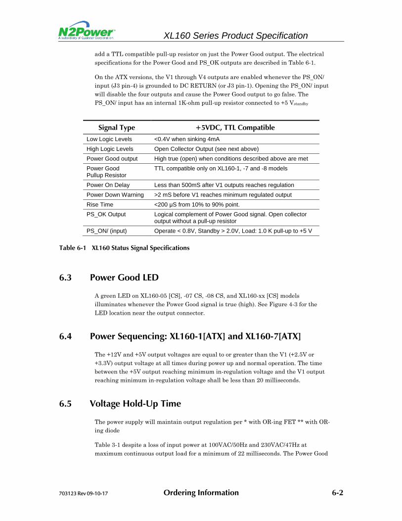
6.2 Power Good Signal/PS_OK Signal/Remote ON Input
The Power Good Signal provides a high logic level to indicate that sufficient time has expired for the DC outputs to be within their regulation limits and that sufficient mains energy is stored by the power supply to ensure continuous power operation within specification for the duration of the hold-up time. When the AC mains power is removed for a period longer than 20ms, the Power Good Signal transitions to a low logic level. The PS_OK signal is the logical complement of the Power Good signal and both signals are driven by open-collector NPN transistors. XL160-1, -7 and -8 models
703123 Rev 09-10-17 Timing and Control 6-1
XL160 Series Product Specification
add a TTL compatible pull-up resistor on just the Power Good output. The electrical specifications for the Power Good and PS_OK outputs are described in Table 6-1.
On the ATX versions, the V1 through V4 outputs are enabled whenever the PS_ON/ input (J3 pin-4) is grounded to DC RETURN (or J3 pin-1). Opening the PS_ON/ input will disable the four outputs and cause the Power Good output to go false. The PS_ON/ input has an internal 1K-ohm pull-up resistor connected to +5 Vstandby
Signal Type +5VDC, TTL Compatible Low Logic Levels <0.4V when sinking 4mA High Logic Levels Open Collector Output (see next above) Power Good output High true (open) when conditions described above are met Power Good Pullup Resistor
TTL compatible only on XL160-1, -7 and -8 models
Power On Delay Less than 500mS after V1 outputs reaches regulation Power Down Warning >2 mS before V1 reaches minimum regulated output Rise Time <200 μS from 10% to 90% point. PS_OK Output Logical complement of Power Good signal. Open collector
output without a pull-up resistor PS_ON/ (input) Operate < 0.8V, Standby > 2.0V, Load: 1.0 K pull-up to +5 V
Table 6-1 XL160 Status Signal Specifications
6.3 Power Good LED
A green LED on XL160-05 [CS], -07 CS, -08 CS, and XL160-xx [CS] models illuminates whenever the Power Good signal is true (high). See Figure 4-3 for the LED location near the output connector.
6.4 Power Sequencing: XL160-1[ATX] and XL160-7[ATX]
The +12V and +5V output voltages are equal to or greater than the V1 (+2.5V or +3.3V) output voltage at all times during power up and normal operation. The time between the +5V output reaching minimum in-regulation voltage and the V1 output reaching minimum in-regulation voltage shall be less than 20 milliseconds.
6.5 Voltage Hold-Up Time
The power supply will maintain output regulation per * with OR-ing FET ** with OR-ing diode
Table 3-1 despite a loss of input power at 100VAC/50Hz and 230VAC/47Hz at maximum continuous output load for a minimum of 22 milliseconds. The Power Good
703123 Rev 09-10-17 Ordering Information 6-2
XL160 Series Product Specification
and PS_OK signals provide a minimum 2mS warning of impending loss of output power.
703123 Rev 09-10-17 Ordering Information 6-3
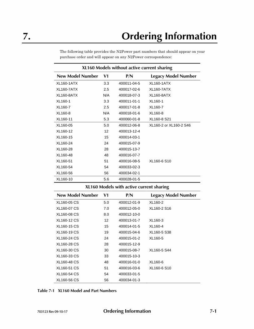
7. Ordering Information The following table provides the N2Power part numbers that should appear on your purchase order and will appear on any N2Power correspondence:
XL160 Models without active current sharing
New Model Number V1 P/N Legacy Model Number XL160-1ATX 3.3 400011-04-5 XL160-1ATX XL160-7ATX 2.5 400017-02-6 XL160-7ATX XL160-8ATX N/A 400018-07-3 XL160-8ATX XL160-1 3.3 400011-01-1 XL160-1 XL160-7 2.5 400017-01-8 XL160-7 XL160-8 N/A 400018-01-6 XL160-8 XL160-11 5.3 400060-01-8 XL160-8 S21 XL160-05 5.0 400012-06-8 XL160-2 or XL160-2 S46 XL160-12 12 400013-12-4 XL160-15 15 400014-03-1 XL160-24 24 400015-07-9 XL160-28 28 400015-13-7 XL160-48 48 400016-07-7 XL160-51 51 400016-08-5 XL160-6 S10 XL160-54 54 400033-02-3 XL160-56 56 400034-02-1 XL160-10 5.6 400028-01-5
XL160 Models with active current sharing
New Model Number V1 P/N Legacy Model Number XL160-05 CS 5.0 400012-01-9 XL160-2 XL160-07 CS 7.0 400012-05-0 XL160-2 S16 XL160-08 CS 8.0 400012-10-0 XL160-12 CS 12 400013-01-7 XL160-3 XL160-15 CS 15 400014-01-5 XL160-4 XL160-19 CS 19 400015-04-6 XL160-5 S38 XL160-24 CS 24 400015-01-2 XL160-5 XL160-28 CS 28 400015-12-9 XL160-30 CS 30 400015-08-7 XL160-5 S44 XL160-33 CS 33 400015-10-3 XL160-48 CS 48 400016-01-0 XL160-6 XL160-51 CS 51 400016-03-6 XL160-6 S10 XL160-54 CS 54 400033-01-5 XL160-56 CS 56 400034-01-3
Table 7-1 XL160 Model and Part Numbers
703123 Rev 09-10-17 Ordering Information 7-1

XL160 Series Product Specification
For warranty information refer to www.n2power.com
All XL160 power supplies are RoHS compliant.
Direct all questions, orders or requests for quotation as follows:
N2Power Order Desk: [email protected] Sales: [email protected]
805-583-7744 x122 Technical Support [email protected]
805-583-7744 x119 Street Address: 130 West Cochran Street, Suite C
Simi Valley, CA 93065
703123 Rev 09-10-17 Ordering Information 7-2