Embed Size (px)
Citation preview

XE166 Family
Hardware Manual XE166 Low End Easy Ki t Board V1.5
Microcontrol lers
Hardware ManualV1.5, 2011-03

Edition 2011-03Published byInfineon Technologies AG81726 Munich, Germany© 2011 Infineon Technologies AGAll Rights Reserved.
LEGAL DISCLAIMERTHE INFORMATION GIVEN IN THIS APPLICATION NOTE IS GIVEN AS A HINT FOR THE IMPLEMENTATION OF THE INFINEON TECHNOLOGIES COMPONENT ONLY AND SHALL NOT BE REGARDED AS ANY DESCRIPTION OR WARRANTY OF A CERTAIN FUNCTIONALITY, CONDITION OR QUALITY OF THE INFINEON TECHNOLOGIES COMPONENT. THE RECIPIENT OF THIS APPLICATION NOTE MUST VERIFY ANY FUNCTION DESCRIBED HEREIN IN THE REAL APPLICATION. INFINEON TECHNOLOGIES HEREBY DISCLAIMS ANY AND ALL WARRANTIES AND LIABILITIES OF ANY KIND (INCLUDING WITHOUT LIMITATION WARRANTIES OF NON-INFRINGEMENT OF INTELLECTUAL PROPERTY RIGHTS OF ANY THIRD PARTY) WITH RESPECT TO ANY AND ALL INFORMATION GIVEN IN THIS APPLICATION NOTE.
InformationFor further information on technology, delivery terms and conditions and prices, please contact the nearest Infineon Technologies Office (www.infineon.com).
WarningsDue to technical requirements, components may contain dangerous substances. For information on the types in question, please contact the nearest Infineon Technologies Office.Infineon Technologies components may be used in life-support devices or systems only with the express written approval of Infineon Technologies, if a failure of such components can reasonably be expected to cause the failure of that life-support device or system or to affect the safety or effectiveness of that device or system. Life support devices or systems are intended to be implanted in the human body or to support and/or maintain and sustain and/or protect human life. If they fail, it is reasonable to assume that the health of the user or other persons may be endangered.

Hardware Manual XE166 Low End Easy Kit Board V1.5
Hardware Manual 3 V1.5, 2011-03
TrademarksTriCore® is a trademark of Infineon Technologies AG.
XE166Revision History: V1.5 2011-03Previous Version(s): 1.4
We Listen to Your CommentsIs there any information in this document that you feel is wrong, unclear or missing? Your feedback will help us tocontinuously improve the quality of this document. Please send your proposal (including a reference to this document) to:[email protected]

Hardware Manual XE166 Low End Easy Kit Board V1.5
Table of Contents
Hardware Manual 4 V1.5, 2011-03
Table of Contents
1 Introduction - XE166 family . . . . . . . . . . . . . . . . . . . . . . . . . . . . . . . . . . . . . . . . . . . . . . . . . . . . . . . . 5
2 General Information about XE166 Easy Kit Board . . . . . . . . . . . . . . . . . . . . . . . . . . . . . . . . . . . . . 62.1 Summary of Features . . . . . . . . . . . . . . . . . . . . . . . . . . . . . . . . . . . . . . . . . . . . . . . . . . . . . . . . . . . . . . 62.2 Block Diagram . . . . . . . . . . . . . . . . . . . . . . . . . . . . . . . . . . . . . . . . . . . . . . . . . . . . . . . . . . . . . . . . . . . 72.3 Board Overview . . . . . . . . . . . . . . . . . . . . . . . . . . . . . . . . . . . . . . . . . . . . . . . . . . . . . . . . . . . . . . . . . . 82.4 DIP Switch S101 . . . . . . . . . . . . . . . . . . . . . . . . . . . . . . . . . . . . . . . . . . . . . . . . . . . . . . . . . . . . . . . . . . 92.4.1 Basic Startup Configuration for XE16x (L/ U -Series) . . . . . . . . . . . . . . . . . . . . . . . . . . . . . . . . . . . 102.5 USB Drive installation . . . . . . . . . . . . . . . . . . . . . . . . . . . . . . . . . . . . . . . . . . . . . . . . . . . . . . . . . . . . . 102.6 Easy Kit Power Supply concept . . . . . . . . . . . . . . . . . . . . . . . . . . . . . . . . . . . . . . . . . . . . . . . . . . . . . 122.6.1 Power Supply via Power Plug . . . . . . . . . . . . . . . . . . . . . . . . . . . . . . . . . . . . . . . . . . . . . . . . . . . . . 13
3 Information in Detail . . . . . . . . . . . . . . . . . . . . . . . . . . . . . . . . . . . . . . . . . . . . . . . . . . . . . . . . . . . . . 143.1 Switch S101 . . . . . . . . . . . . . . . . . . . . . . . . . . . . . . . . . . . . . . . . . . . . . . . . . . . . . . . . . . . . . . . . . . . . 143.1.1 DIP Switch Setting for XE16x (L/ U -Series) . . . . . . . . . . . . . . . . . . . . . . . . . . . . . . . . . . . . . . . . . . 143.2 Headers, Connectors and Components . . . . . . . . . . . . . . . . . . . . . . . . . . . . . . . . . . . . . . . . . . . . . . . 153.2.1 USB Interface . . . . . . . . . . . . . . . . . . . . . . . . . . . . . . . . . . . . . . . . . . . . . . . . . . . . . . . . . . . . . . . . . 153.2.2 CAN0 (X106) . . . . . . . . . . . . . . . . . . . . . . . . . . . . . . . . . . . . . . . . . . . . . . . . . . . . . . . . . . . . . . . . . . 153.2.3 LIN Interface (X105) . . . . . . . . . . . . . . . . . . . . . . . . . . . . . . . . . . . . . . . . . . . . . . . . . . . . . . . . . . . . 163.2.4 OCDS Interface . . . . . . . . . . . . . . . . . . . . . . . . . . . . . . . . . . . . . . . . . . . . . . . . . . . . . . . . . . . . . . . . 163.2.5 DAP Interface . . . . . . . . . . . . . . . . . . . . . . . . . . . . . . . . . . . . . . . . . . . . . . . . . . . . . . . . . . . . . . . . . 163.2.6 ADC . . . . . . . . . . . . . . . . . . . . . . . . . . . . . . . . . . . . . . . . . . . . . . . . . . . . . . . . . . . . . . . . . . . . . . . . . 173.2.7 LEDs . . . . . . . . . . . . . . . . . . . . . . . . . . . . . . . . . . . . . . . . . . . . . . . . . . . . . . . . . . . . . . . . . . . . . . . . 173.2.8 Serial EEPROM . . . . . . . . . . . . . . . . . . . . . . . . . . . . . . . . . . . . . . . . . . . . . . . . . . . . . . . . . . . . . . . . 173.3 Pin Definition and Location . . . . . . . . . . . . . . . . . . . . . . . . . . . . . . . . . . . . . . . . . . . . . . . . . . . . . . . . . 183.3.1 64 - Pinout . . . . . . . . . . . . . . . . . . . . . . . . . . . . . . . . . . . . . . . . . . . . . . . . . . . . . . . . . . . . . . . . . . . . 183.3.2 48 - Pinout . . . . . . . . . . . . . . . . . . . . . . . . . . . . . . . . . . . . . . . . . . . . . . . . . . . . . . . . . . . . . . . . . . . . 203.3.3 38 - Pinout . . . . . . . . . . . . . . . . . . . . . . . . . . . . . . . . . . . . . . . . . . . . . . . . . . . . . . . . . . . . . . . . . . . . 223.4 Zero Ohm Resistors . . . . . . . . . . . . . . . . . . . . . . . . . . . . . . . . . . . . . . . . . . . . . . . . . . . . . . . . . . . . . . 23
4 Getting Started . . . . . . . . . . . . . . . . . . . . . . . . . . . . . . . . . . . . . . . . . . . . . . . . . . . . . . . . . . . . . . . . . 244.1 Power Supply . . . . . . . . . . . . . . . . . . . . . . . . . . . . . . . . . . . . . . . . . . . . . . . . . . . . . . . . . . . . . . . . . . . 244.2 BMI Programming . . . . . . . . . . . . . . . . . . . . . . . . . . . . . . . . . . . . . . . . . . . . . . . . . . . . . . . . . . . . . . . . 244.3 OCDS Debugging Interface . . . . . . . . . . . . . . . . . . . . . . . . . . . . . . . . . . . . . . . . . . . . . . . . . . . . . . . . 244.4 USB Interface for UART support . . . . . . . . . . . . . . . . . . . . . . . . . . . . . . . . . . . . . . . . . . . . . . . . . . . . 24
5 Schematic . . . . . . . . . . . . . . . . . . . . . . . . . . . . . . . . . . . . . . . . . . . . . . . . . . . . . . . . . . . . . . . . . . . . . 25

Hardware Manual XE166 Low End Easy Kit Board V1.5
Introduction - XE166 family
1 Introduction - XE166 family XE166 family - More performance, more Flash, better peripherals
With more than 15 successful years in the microcontroller market place, C166 has set the standard for 16-bitarchitectures with the highest aggregate volume share of all available 16-bit devices. With its fast interrupt response and context switching, the C166 family is ideally suited for automotive, industrial,mass storage and wired as well as wireless communications applications.Compared with the XC166, XE166 delivers more performance, more Flash memory, more RAM, stronglyenhanced peripherals and a complete DSP library.
MCU and DSP in a core
Infineon Technologies´ Real Time Signal Controller combines the traditional strengths of a Microcontroller Unit(MCU) to control peripherals with the computing power of Digital Signal Processors (DSP). All in one enhancedC166S V2 core. Together, the Microcontroller's real-time capability and ease of use and the DSP's mathematicalperformance and data throughput form a powerful singe-chip solution ideal for many embedded applications.
For detailed technical information about the different derivatives please refer to the XE166 family web pages onthe Infineon Internet.
http://www.infineon.com/XE166
This document covers all products of the XE162xL, XE161xL, XE161FU and XE160FU series.
Hardware Manual 5 V1.5, 2011-03

Hardware Manual XE166 Low End Easy Kit Board V1.5
General Information about XE166 Easy Kit Board
2 General Information about XE166 Easy Kit Board
2.1 Summary of Features
� Infineon�s XE166 Controller in LQFP-64, VQFN-48 and TSSOP-38 Package� High Speed CAN Transceiver, LIN Transceiver, USB to UART/JTAG bridge� 8 Low Power Status LEDs� Easy access to all pins � 4-DIP switches for configuration� On board USB to JTAG/UART interface� Powered via USB
ConnectorsThe XE166 Board offers a wide variety of connectors:
� USB connector for ASC/ JTAG/ SPD Interface� 4-pin header for LIN Transceiver � 16-pin header for JTAG interface (OCDS)� 10-pin (2x5) header for CAN High Speed Transceiver (CAN0)� 10-pin header for DAP/ SPD interface
Components� Low-Drop Voltage Regulator TLE 4274� Four status LED´s for Power/RESET/JTAG� CAN-Transceiver TLE 6251DS� LIN Transceiver TLE 7259� FT2232HL Dual USB to UART/JTAG interface � SPI EEPROM 128 Kbit AT25128N1)
� 8 general purpose LEDs� Potentiometer for ADC� Reset switch
Zero Ohm Bridges� Zero Ohm resistors give the flexibility to configure the systems functionality
1) The soldered part may differ from the schematic, for example Atmel 25040AN.
Hardware Manual 6 V1.5, 2011-03

Hardware Manual XE166 Low End Easy Kit Board V1.5
General Information about XE166 Easy Kit Board
2.2 Block Diagram
Figure 1 Block diagram of XE166 Easy Kit layout overview
XE16xCPU
OC
DS
1
XTAL
USB To UART/JTAG Bridge
TxD
RxDM
ultiC
AN
Voltage Regulator
LIN Transceiver
CAN Transceiver
8 LEDs
EEPROMLIN
USB
DA
P
Hardware Manual 7 V1.5, 2011-03

Hardware Manual XE166 Low End Easy Kit Board V1.5
General Information about XE166 Easy Kit Board
2.3 Board Overview
Figure 2 Top View (basic components)
USB
Power1
LIN11
CAN0
Config1 4
InfineonXE166
Reset
Debug Run
Debug Active
Power Supply
1
Power Supply Jumper
DAP
1 1
OCDS110.7
AN0 (ADC)
Reset
Hardware Manual 8 V1.5, 2011-03

Hardware Manual XE166 Low End Easy Kit Board V1.5
General Information about XE166 Easy Kit Board
Figure 3 Top view in detail
2.4 DIP Switch S101Although most of the programmable features of the XE166 are selected by software either during the initializationphase or repeatedly during program execution, some features must be selected earlier because they are used forthe first access of the program execution.These configurations are accomplished by latching the logic levels at a number of pins at the end of the internalreset sequence.DIP switch S101 allows to configure the startup setting of the XE166 during RESET. The default System StartupConfiguration is shown in Table 1. By default all DIP Switches are OFF. The XE166 executes a standard start frominternal Flash. Note: The Kit is programmed with BMI for DAP. To connect a JTAG debugger box from a Tool vendor (KEIL, PLS),
the BMI need to be reprogrammed to JTAG using a flash programming software (e.g. Memtool).
Table 1 Default ConfigurationName in
schematicDefault configuration Description
S101 Startup configuration:Standard start from internal Flash (Default)
P2.9 P10.12 /TRST ADBUS5
32 41
On
Off
Hardware Manual 9 V1.5, 2011-03

Hardware Manual XE166 Low End Easy Kit Board V1.5
General Information about XE166 Easy Kit Board
2.4.1 Basic Startup Configuration for XE16x (L/ U -Series)
Configuration pins are treated by firmware differently depending on additional conditions:1. If TRST=0 - it is purely hardware controlled (so-called �Zero-pin�) configuration - device start from Internal Flashwithout debug support is executed2. If TRST=1 - the Boot Mode Index (BMI) is evaluated by firmware first and depending on the result - start-upmode and debug
For more detailed information about the DIP switch setting, please refer to Chapter 3.1.1, Table 4.
2.5 USB Drive installationAll USB-Transaction are realized by the USB-Software running on a Host-Computer. The USB-Device driver iscommunicating with the Equipment connected to the Computer. The driver for Easy Kit USB interface will be delivered with a Software called DAS (Device Access Server). Thegoal of the DAS architecture is to provide one single interface for all types of tools, which fulfills all performanceand reliability needs. Additionally a driver for a virtual COM port will be installed. Find out more about DAS on the Infineon Web page:
http://www.infineon.com/DAS
This DAS Software can be found in the Easy Kit CD under the Tools section. DAS Software Version 3.0.0 or higheris required to be used with the Easy Kit.
Table 2 Basic Startup Configuration via External CircuitryStartup Mode TRST BMI value1)
1) BMI0[15:12] = 0101B means BMI.BLS=enable.BMI0[15:12] = 1010B means BMI.BLS=disable.
BMI0[15:12] = else means BMI is invalid.
CFG-pins P2.9 P10.12
Internal Start from Flash, no debug 0 not checked x x
Start-up and debug mode from BMI 1 BMI valid BMI.BLS=disable x xStart-up and debug mode from BMI BMI.BLS=enable x 0ASC Bootloader x 1ASC Bootloader BMI invalid/ unconfigured x 1
CAN Bootloader 2)
2) CAN Bootloader is not available to XE16xU series.
0 0
Internal start from Flash,JTAG debug pos.A
1 0
Hardware Manual 10 V1.5, 2011-03
Hardware Manual XE166 Low End Easy Kit Board V1.5
General Information about XE166 Easy Kit Board
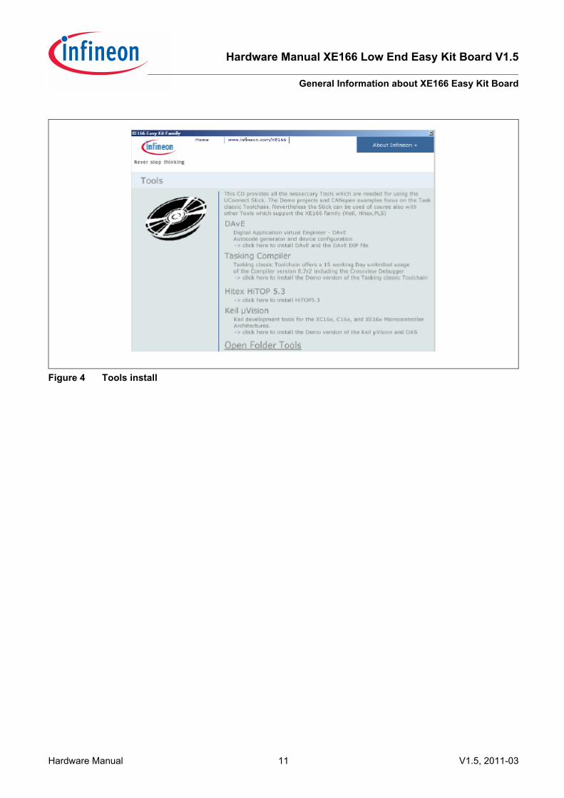
Figure 4 Tools install
Hardware Manual 11 V1.5, 2011-03

Hardware Manual XE166 Low End Easy Kit Board V1.5
General Information about XE166 Easy Kit Board
2.6 Easy Kit Power Supply conceptThe Easy Kit USB Power Supply concept allows the user to work with the Kit without an external Power Supply.If the USB power supply is not sufficient, an additional regulated DC power supply can be used.
Figure 5 Easy Kit Power Supply concept
By means of the Power Supply Jumper JP201, USB, or the external power Supply can be selected to run the EasyKit. The Setup for the Jumper JP201 is shown in Table 3 below.
The USB specification provides a 5 V supply on a single wire from which connected USB devices may draw power.The specification provides for no more than 5.25 V and no less than 4.35 V between the +ve and -ve bus powerlines.Initially, a device is only allowed to draw 100 mA. It may request more current from the upstream device in unitsof 100 mA up to a maximum of 500 mA. In practice, most ports will deliver the full 500 mA or more before shuttingdown power, even if the device hasn't requested it or even identified itself. If a (compliant) device requires morepower than is available, then it cannot operate until the user changes the network (either by rearranging USBconnections or by adding external power) to supply the required power.
Table 3 Power Supply Jumper configurationName in schematic
Configuration Description
JP201Power Supply via USB Interface(Default)
JP201Power Supply via Power Plug
Power SupplyUSB Supply
PowerLEDs
JP201
1
DC
6 � 12V5V
5V
XE166CPU
1 2 3
2 31
Hardware Manual 12 V1.5, 2011-03

Hardware Manual XE166 Low End Easy Kit Board V1.5
General Information about XE166 Easy Kit Board
Note: If the USB power supply is not sufficient, an external power supply is needed and the Jumper JP201 setting need to be changed.
Note: In case the USB Host PC goes into Suspend Mode, an external Power Supply should be used.
2.6.1 Power Supply via Power PlugThe XE166 Board can be supplied either with USB cable or with an external power supply. For external powersupply, a regulated DC power supply with max. 12Volt/ 400mA can be connected to the power connector. Themaximum power dissipation of the used voltage regulator has to be taken into account.
Figure 6 Power Supply
Hardware Manual 13 V1.5, 2011-03

Hardware Manual XE166 Low End Easy Kit Board V1.5
Information in Detail
3 Information in DetailThe XE166 family supports variety of start-up modes, allowing the user to make selections in three aspects:� Main functionality - where from the user code will be started (on-chip Flash, PSRAM, external memory);� Optionally - a way for initial code-downloading into PSRAM before to start it:
� From an external host via a communication interface - UART, CAN.� Debug-related - either debugging will be possible, and if Yes - which debug-interface to use (SPD, JTAG, and
DAP selectable pin-assignments via BMI).The Easy Kit Board Manual covers only a limited number of start-up modes. For all possible start-up modes pleaserefer to the corresponding User�s Manual.
3.1 Switch S101
3.1.1 DIP Switch Setting for XE16x (L/ U -Series)
Table 4 DIP Switch Settings for S101Name in
schematicDefault configuration Description
S101 Startup configuration:Standard start from internal Flashxx-xx-OFF-xx
S101 Startup configuration:BMI valid. BLS disable,Start-up and debug mode from BMIxx-xx-ON-xx
S101 Startup configuration:BMI valid. BLS enable,Start-up and debug mode from BMIxx-ON-ON-xx
S101 Startup configuration:BMI valid. BLS enable,Bootstrap loader ASCxx-OFF-ON-xx
S101 Startup configuration:BMI invalid.Bootstrap loader ASCxx-OFF-ON-xx
S101 Startup configuration:BMI invalid.Bootstrap loader CANON-ON-ON-xx
32 41
On
Off
32 41
On
Off
32 41
On
Off
32 41
On
Off
32 41
On
Off
32 41
On
Off
Hardware Manual 14 V1.5, 2011-03

Hardware Manual XE166 Low End Easy Kit Board V1.5
Information in Detail
Note: Other than hardware configuration, the BMI value has to be configured in order for the device to run in the correct mode. For more information, refer to Table 2.
3.2 Headers, Connectors and Components
3.2.1 USB InterfaceThe USB connector is used for connection to a PC. Via the USB it is possible to power the board, using the USIC0Channel 0 as serial connection via USB and Debugging via DAS. For the pinout of USB socket see Figure 7.
Figure 7 On-board header (P201)
3.2.2 CAN0 (X106)One CAN transceiver is connected to the MultiCAN on XE166 node 0. The transceiver is connected to the IDC10plug. For the pinout of IDC10 plug see Figure 8. You can use a IDC female connector with crimp connector, flatcable and SUB-D 9 plug with crimp connector to have a 1:1 adapter to SUB-D 9. CAN module is not available to XE16xU series.
Figure 8 On-board header (X106)
S101 Startup configuration:BMI invalid.JTAG Debug Mode AOFF-ON-ON-xx
S101 Startup configuration:All other positions are reserved
Table 4 DIP Switch Settings for S101Name in
schematicDefault configuration Description
32 41
On
Off
1 (Vbus)2 (D-)
3 (D+) 4 (GND)
2
4
6
8
1
3
5
7
9 10
GND
GND
CANL CANH
VDDP
Hardware Manual 15 V1.5, 2011-03
Hardware Manual XE166 Low End Easy Kit Board V1.5
Information in Detail
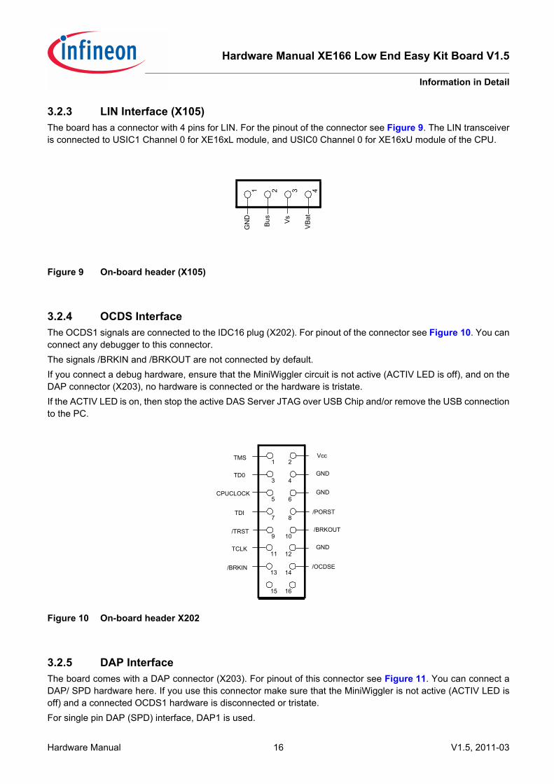
3.2.3 LIN Interface (X105)The board has a connector with 4 pins for LIN. For the pinout of the connector see Figure 9. The LIN transceiveris connected to USIC1 Channel 0 for XE16xL module, and USIC0 Channel 0 for XE16xU module of the CPU.
Figure 9 On-board header (X105)
3.2.4 OCDS InterfaceThe OCDS1 signals are connected to the IDC16 plug (X202). For pinout of the connector see Figure 10. You canconnect any debugger to this connector. The signals /BRKIN and /BRKOUT are not connected by default. If you connect a debug hardware, ensure that the MiniWiggler circuit is not active (ACTIV LED is off), and on theDAP connector (X203), no hardware is connected or the hardware is tristate. If the ACTIV LED is on, then stop the active DAS Server JTAG over USB Chip and/or remove the USB connectionto the PC.
Figure 10 On-board header X202
3.2.5 DAP InterfaceThe board comes with a DAP connector (X203). For pinout of this connector see Figure 11. You can connect aDAP/ SPD hardware here. If you use this connector make sure that the MiniWiggler is not active (ACTIV LED isoff) and a connected OCDS1 hardware is disconnected or tristate.For single pin DAP (SPD) interface, DAP1 is used.
1 2 3 4
GN
D VsBus
VB
at
2
4
6
8
1
3
5
7
9 10
Vcc
CPUCLOCK
TD0 GND
/PORST
12
14
11
13
15 16
/OCDSE
/BRKOUT
GND
GND
/TRST
TMS
TCLK
TDI
/BRKIN
Hardware Manual 16 V1.5, 2011-03

Hardware Manual XE166 Low End Easy Kit Board V1.5
Information in Detail
Figure 11 On-board header X203
3.2.6 ADCOn AN0 (ADC0) is a 10K potentiometer (R113) connected. You can apply a voltage between VAGND0 andVAREF0 to the AN0 channel via this potentiometer.
3.2.7 LEDsPort 10 pin 0 up to pin 7 are connected to single LED�s (D101... D108) and can be controlled by Software. Thesestatus LEDs are low active.
3.2.8 Serial EEPROMBy default the USIC0 Channel 1 of the XE166 is connected to a serial EEPROM with a size of 512K (64 x 8). Thedefault setting for the SSC is described in Table 6.
Table 5 LEDs descriptionLED number DescriptionD201 (red) Debug Run Mode (switched by DAS Server)D202 (green) Debug Active (Mini Wiggler circuit active)D207 (red) Power On Reset Active D208 (green) Board Voltage 5 VoltsD101 - D108 (yellow) Status of P10L
Table 6 Serial EEPROM interfaceDefault Setting:SSC (USIC0 Channel 1)P2.8 (SCK) with R140 P2.4 (SI) with R141 P2.10 (SO) with R142 P2.7 (CS) with R143
1
3
5
7
2
4
6
8
9 10
VREF
GND
DAP1
DAP0
USER1_IN
/RESET
GND
GND
USER0_IO
Hardware Manual 17 V1.5, 2011-03
Hardware Manual XE166 Low End Easy Kit Board V1.5
Information in Detail
3.3 Pin Definition and Location
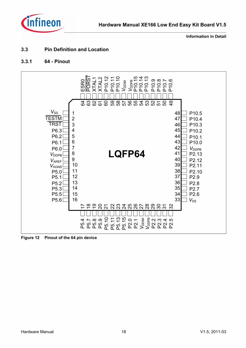
3.3.1 64 - Pinout
Figure 12 Pinout of the 64 pin device
16151413121110987654321 48
474645444342414039383736353433
LQFP645051 4952535455565758596061626364
3130 3229282726252423222120191817
P5.6P5.5P5.3P5.2P5.1P5.0
VAGND
TESTM
P6.3
VAREF
VDDPB
P6.2P6.1P6.0
P2.7P2.8P2.9P2.10P2.11P2.12P2.13
P2.6
P10.4
VDDPB
P10.0
P10.3P10.2P10.1
P10.5
P10.
7P1
0.8
P10.
9
P10.
10P1
0.11
P10.
12
P10.
13
POR
ST
V DD
IM
P10.
14
XTAL
1XT
AL2
P10.
15
ESR
0
V DD
PB
P2.5
P2.4
P2.3
P2.2
P2.1
P2.0
P5.1
5
V DD
PB
P5.7
P5.8
P5.9
V DD
IM
P5.1
3
P5.1
0P5
.11
P5.4
TRST
P10.
6
VSS
VSS
Hardware Manual 18 V1.5, 2011-03
Hardware Manual XE166 Low End Easy Kit Board V1.5
Information in Detail
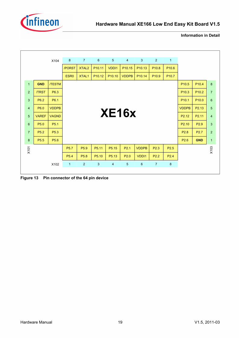
Figure 13 Pin connector of the 64 pin device
GNDP2.6
P2.7P2.8
P2.9P2.10
P2.11P2.12
P2.13VDDPB
P10.0P10.1
P10.2P10.3
P10.4P10.5
1
2
3
4
5
6
7
8
P5.4
P5.7
P5.8
P5.9
P5.10
P5.11
P5.13
P5.15
P2.0
P2.1
VDDI1
VDDPB
P2.2
P2.3
P2.4
P2.5
1 2 3 4 5 6 7 8X102
X10
3
ESR0
/PORST
XTAL1
XTAL2
P10.12
P10.11
P10.10
VDDI1
VDDPB
P10.15
P10.14
P10.13
P10.9
P10.8
P10.7
P10.6
P5.6P5.5
P5.3P5.2
P5.1P5.0
VAGNDVAREF
VDDPBP6.0
P6.1P6.2
P6.3/TRST
/TESTMGND
8
7
6
5
4
3
2
1
X10
1
8 7 6 5 4 3 2 1X10⁴
XE16x
Hardware Manual 19 V1.5, 2011-03

Hardware Manual XE166 Low End Easy Kit Board V1.5
Information in Detail
3.3.2 48 - Pinout
Figure 14 Pinout of the 48 pin device
121110987654321 36
3534333231302928272625
VQFN48
373839404142434445464748
242322212019181716151413
P5.3P5.2
VDDPB
TESTM
P6.3P6.1
VAGND
VAREF
P6.0
P5.0
P2.6P2.7P2.8
P10.4
P10.0
P10.3P10.2P10.1
P10.5
P10.
6P1
0.7
P10.
12
POR
ST
V DD
IM
XTAL
2
P10.
9P1
0.8
V DD
PB
P2.2
P2.1
P2.0
V DD
PB
P2.3
P5.8
P5.9
V DD
IM
P2.5
P2.4
XTA
L1TRST
P5.4
P2.9P2.10P2.13
P10.
10
VSSV S
SV S
S
Hardware Manual 20 V1.5, 2011-03

Hardware Manual XE166 Low End Easy Kit Board V1.5
Information in Detail
Figure 15 Pin connector of the 48 pin device
ncP2.6
P2.7P2.8
P2.9P2.10
ncnc
P2.13nc
P10.0P10.1
P10.2P10.3
P10.4P10.5
1
2
3
4
5
6
7
8
P5.4
nc
P5.8
P5.9
nc
nc
nc
nc
P2.0
P2.1
VDDI1
VDDPB
P2.2
P2.3
P2.4
P2.5
1 2 3 4 5 6 7 8X102
X10
3
nc
/PORST
XTAL1
XTAL2
P10.12
nc
P10.10
VDDI1
VDDPB
nc
nc
nc
P10.9
P10.8
P10.7
P10.6
ncnc
P5.3P5.2
ncP5.0
VAGNDVAREF
VDDPBP6.0
P6.1nc
P6.3/TRST
/TESTMnc
8
7
6
5
4
3
2
1
X10
1
8 7 6 5 4 3 2 1X10⁴
XE16x
Hardware Manual 21 V1.5, 2011-03
Hardware Manual XE166 Low End Easy Kit Board V1.5
Information in Detail
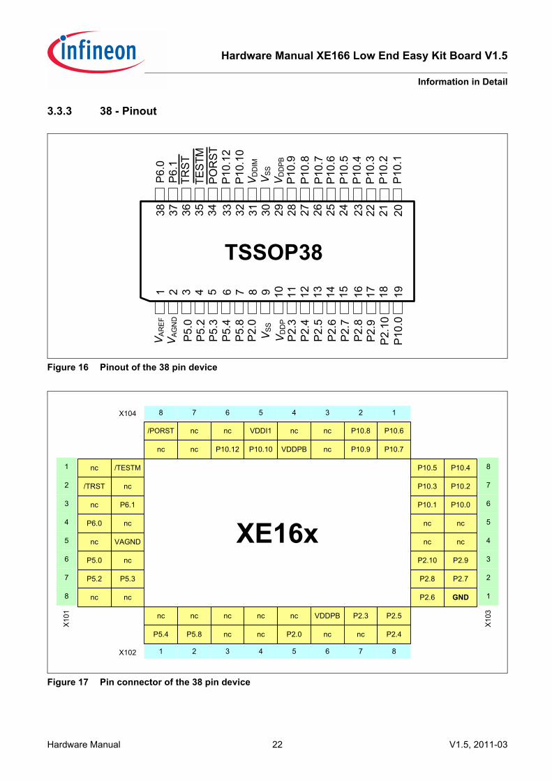
3.3.3 38 - Pinout
Figure 16 Pinout of the 38 pin device
Figure 17 Pin connector of the 38 pin device
2122 20P
10.1
TSSOP38
2425 2326272829303132333435363738
1514 1613121110987654321
P10.
2P1
0.3
P10.
4P1
0.5
P10.
6
P10.
12PO
RST
V DD
IM
P10.
7
P10.
10
P10.
9P1
0.8
TRST
V DD
PB
P2.4
P2.3
P2.0
TEST
M
P5.8
P5.4
P5.3
V DD
P
P6.
0P
6.1
V AR
EF
P5.2
V AG
ND
P5.0
P2.5
1817 19
P2.7
P2.6
P2.8
P2.9
P10.
0P2
.10
V SS
V SS
GNDP2.6
P2.7P2.8
P2.9P2.10
ncnc
ncnc
P10.0P10.1
P10.2P10.3
P10.4P10.5
1
2
3
4
5
6
7
8
P5.4
nc
P5.8
nc
nc
nc
nc
nc
P2.0
nc
nc
VDDPB
nc
P2.3
P2.4
P2.5
1 2 3 4 5 6 7 8X102
X10
3
nc
/PORST
nc
nc
P10.12
nc
P10.10
VDDI1
VDDPB
nc
nc
nc
P10.9
P10.8
P10.7
P10.6
ncnc
P5.3P5.2
ncP5.0
VAGNDnc
ncP6.0
P6.1nc
nc/TRST
/TESTMnc
8
7
6
5
4
3
2
1
X10
1
8 7 6 5 4 3 2 1X10⁴
XE16x
Hardware Manual 22 V1.5, 2011-03

Hardware Manual XE166 Low End Easy Kit Board V1.5
Information in Detail
3.4 Zero Ohm ResistorsFor configuration purposes several zero ohm resistors have been implemented. The functionality of these resistorsare shown in the table below. Table 7 Zero Ohm ResistorsComponent Name in
schematicDescription
TLE7259(LIN Transceiver Board)
For XE16xL seriesFor XE16xU series
R124
R125 / R126R149 / R150
enable / disable
connect / disconnect connect / disconnect
TLE6251DS(CAN Transceiver)1)
1) CAN transceiver is not available to XE16xU series.
R129 / R130R131R135R133 / 134
connect / disconnect (CAN0)enable / disable (CAN0) supply Bus voltage internal / external (CAN0)connect Bus / disconnect Bus (CAN0)
Microcontroller XE16xAnalog reference
Voltage supply
R148R213R147
change of analog reference source
change of voltage supplyAT25128N 2)
(Serial EEPROM)
2) The soldered part may differ from the schematic, for example Atmel 25040AN.
R140 / R141R142 / R143
connect to USIC0 Channel 1connect to USIC0 Channel 1
Status LED´sOscillator circuit
R109R115 / R116
connect / disconnect LED´s to 5 V oscillator gain
FT2232HL
JTAG-Option:
DAP-Option:
ASC Bootloader:64 Pin / 48 Pin/ 38 Pin
Other
U203:
EEPROM 93LC46B:
R233, R238
R233, R238
R236-R237
R236-R237
R210
R207
open
assembled with 0R
assembled with 0R
open
For internal use only
If ORG functionality is needed
Hardware Manual 23 V1.5, 2011-03
Hardware Manual XE166 Low End Easy Kit Board V1.5
Getting Started
4 Getting Started
4.1 Power SupplyIf more current is needed, a regulated DC power supply with max. 12 Volts should be connected to the powerconnector. The maximum power dissipation of the used voltage regulator has to be taken into account. By defaultone green LED should be active. It indicates that the embedded voltage regulator supply the microcontroller.Note: Power supply is not part of the delivery.
Figure 18 Power Supply Connector
4.2 BMI ProgrammingThe XE166 Easy Kit supports Boot Mode Index (BMI) programming. This provides flexibility for the users toconfigure the device start-up mode. BMI value can be configured via software or tool. For details on how to program the BMI value, please refer to the User�s Manual.
4.3 OCDS Debugging InterfaceThe XE166 Easy Kit offers access to device via four interfaces (UART, JTAG, DAP, SPD), through a USBconnection. With the FTDI chip, an on board USB JTAG wiggler has been implemented. Further, the USB interfaceallows to emulate a USB to UART bridge.A simple 16-pin JTAG/ DAP/ SPD header can be used to connect a debugger from one of Infineon�s tool suppliers.Both systems include an On-Chip Debug Support (OCDS) system, which provides convenient debugging,controlled directly by an external device via debug interface pins.
4.4 USB Interface for UART supportThe USB connector is used for connection to a PC. Via the USB it is possible to power the board, using the ASCas serial connection via USB and Debugging via DAS. For the pinout of USB socket see Figure 7.Note: Before connecting the board to the PC, make sure that the actual DAS software is installed on the PC. For
actual DAS software please contact your local FAE.
The latest version of the software can also be found on the DAS website:
www.infineon.com/DAS
Hardware Manual 24 V1.5, 2011-03

Hardware Manual XE166 Low End Easy Kit Board V1.5
Schematic
5 Schematic
11
22
33
44
55
66
77
88
DD
CC
BB
AA
1Infineon Technologies AG
ATV M
C ACE PDA
Am Cam
peon 1-12
D-85579 Neubiberg
Tel.: +49-89-234-0
3
29.09.2010
Number:
Date:
Sheet:
of
Easy K
it XC2XXX 64/48/38 CPU and O
n Board
IO's
1.1
Revision:
G:\Technical_Support\P11\XC2XXX\EDA_DXP\Easy Kit XC2XXX\64_48_38 V1.X\Easy Kit xc2xxx 64_48_38 V1.1\M
ain.Sch
File:
R115
0R
1 2
Y101
8MHz
C103
18pF
C102
18pF
GND
GND
+5V
R131
0R
GND
R132
120R
R133
0R
R134
0R
CB102
100n
GND
R135
0R_opt
+5V
GNDR124
0R
+5V
R128
1K
CB101
100n
GND
C105
22µF/50V
GND
+5V R109
0R
R110
0R
+5V
P2.0
P2.2
P2.3
P2.4
P2.5
P2.6
P2.7
/TESTM
XTAL1
XTAL2
/PORST
C101
1n
GND
P5.0
P5.1
P5.2
P5.3
P5.4
P5.5
P5.6
P5.7
P5.10
P5.11
P5.13
P5.15
P2.13
P2.5
P2.3
P10.15
P10.13
P10.0
P10.1
P10.2
P10.3
P10.4
P10.5
P10.6
P10.7
/TRST
R101
1K5
R102
1K5
R103
1K5
R104
1K5
R105
1K5
R106
1K5
R107
1K5
R108
1K5
P2.8
P2.9
P2.10
P2.11
P2.12
P6.3
P2.1
D101
LY T67K
D102
LY T67K
D103
LY T67K
D104
LY T67K
D105
LY T67K
D106
LY T67K
D107
LY T67K
D108
LY T67K
R111
47K
GND
R114
100R
1 3
2R113
10K
C104
100n
VAGNDP5.0
VAGND
VAREF
1 32 4
X105
LIN
GND
VBAT
R116
opt
R126
0R
R125
0R
R130
0R
R129
0R
/TRST
P5.9
P5.8
P10.7
P10.6
P10.5
P10.4
P10.3
P10.2
P10.1
P10.0
1 3 5 7 9 111315
2 4 6 810121416
X102
CPUCON2_opt
HOLD
7
WP
3
VCC
8
CS
1
GND
4
SO
2
SCK
6
SI
5
U107
AT25128N-10SI2.7
CB104
100n
R144
10K
R145
10K
R146
10K
GND
+5V
P2.8
P2.4
P2.10
P2.7
TRST
3
XTAL162
XTAL261
PORST63
TESTM
2
P5.0
11
P2.025
P2.126
P2.229
P2.330
P2.431
P2.532
P5.417
P2.7
35
P2.9
37
P2.10
38
P2.8
36
P6.0
7P6.1
6
P6.3
4
P10.0
43
P10.1
44
P10.2
45
P10.3
46
P10.4
47
P10.5
48
P10.649
P10.750
P10.851
P10.952
P10.1058
P10.1159
P10.1260
P10.1353
P10.1454
P10.1555
ESR064
VDDI157
VDDPB
8
VDDPB28
VDDPB56
GND
1
VDDPB
42
GND
33
VDDI127
VAGND
10
VAREF
9
P6.2
5
P5.1
12
P5.2
13
P5.3
14
P5.5
15
P5.6
16
P5.718
P5.819
P5.920
P5.1021
P5.1122
P5.1323
P5.1524
P2.11
39
P2.13
41
P2.12
40
P2.6
34U101
XC2XXX LE 64 PIN
P10.15
P10.14
P10.13
P10.12
P10.11
P10.10
P10.9
P10.8
ESR0
GND
2
RXD
4CANH
7
TXD
1
VCC
3
CANL
6
STB
8
SPLIT
5U105
TLE6251DS
1X10⁸
SPLIT_CAN0_opt
1 2 3 4
8 7 6 5
1
S101
CONFIG
P10.12
/TRST
P2.9
R121
2K8
R122
0R
R127
10K
+5V
R119
470R
R120
470R
1 3 5 7 9
2 4 6 810
X106
CAN0
R140
0R
R141
0R
R142
0R
R143
0R
PORT[2..10]
GND
13
2D109
BAT54-04
R112
10K
1 32
X107
I2C_opt
P10.1
P10.2
GND
TRST
36
PORST
34
TESTM
35
P5.0
3
P2.0
8
P2.3
11
P2.4
12
P2.5
13
P2.6
14
P2.7
15
P2.9
17
P2.8
16
P6.0
38
P6.1
37
P10.0
19
P10.1
20
P10.2
21
P10.3
22
P10.4
23
P10.5
24
P10.6
25
P10.7
26
P10.8
27
P10.9
28
P10.10
32
P10.12
33
VDDI1
31
VDDPB
10
VDDPB
29
GND
30
VAGND
2VAREF
1
P5.2
4
P5.3
5
P5.4
6
P5.8
7
GND
9
P2.10
18
U103
XC2XXX ULE 38 PIN
TRST
2
XTAL147
XTAL246
PORST48
TESTM
1
P5.0
10
P2.016
P2.117
P2.221
P2.322
P2.423
P2.524
P2.6
25
P2.8
27
P2.9
28
P2.7
26
P6.0
5P6.1
4P6.3
3
P10.0
31
P10.1
32
P10.2
33
P10.3
34
P10.4
35
P10.5
36
P10.637
P10.738
P10.839
P10.940
P10.1044
P10.1245
VDDI143
VDDPB
7
VDDPB20
VDDPB41
VDDI118
VAGND
9VAREF
8
P5.2
11
P5.3
12
P5.413
P5.814
P5.915
GND
6
GND19
GND42
P2.10
29
P2.13
30U102
XC2XXX LE_ULE 48 PIN
1 3 5 7 9 111315
2 4 6 810121416
X103
CPUCON3_opt
1 3 5 7 9 111315
2 4 6 810121416
X101
CPUCON1_opt
1 3 5 7 9 111315
2 4 6 810121416
X104
CPUCON4_opt
VDDPB
VDDI1
VDDPB
XTAL1
XTAL2
GND
VDDPB
VAREF
VAGND
VDDI1
VDDPB
GND
+5V
P6.0
P6.1
P6.2
/TESTM
ESR0
P2.0
P2.2
P2.3
P2.4
P2.5
P2.6
/TESTM
/PORST
P5.0
P5.2
P5.3
P2.8
P2.9
P2.10
P6.3
P2.1
/TRST
P5.9
P5.8
P10.7
P10.6
P10.5
P10.4
P10.3
P10.2
P10.1
P10.0
P10.12
P10.10
P10.9
P10.8
VDDI1
VDDPB
XTAL1
XTAL2
GND
VDDPB
VAREF
VAGND
VDDI1
VDDPB
P6.0
P6.1
GND
GND
GND
GND
+5V
R136
1K_opt
R137
1K_opt
+5V
+5V
VDD
3
ALERT
5
GND
2SDA
6
SCL
4
AS
1
U106
AD7414ART_opt
R138
opt
R139
opt
GND
+5V
CB103
100n_opt
GND
+5V
VDDPB
VAREF
VAGND
VDDPB
VDDI1
GND
GND
P5.3
P6.1
P2.3
P2.5
P2.8
P2.10
P10.5
P10.3
P10.1
/TRST
P10.7P10.9
P5.0
P5.2
P5.4
P6.0
P2.0
P2.4
P2.6
P5.8
P2.7
P2.9
P10.6
P10.4
P10.2
P10.0
/TESTM
/PORST
P10.12
P10.10
P10.8
CB109
100n
R148
0R
R123
0R
+5V
GND
VAREF
VAGND
CB114
100n
VAGND
VAGND
CB111
470n
CB115
470n
VDDI1 CB110
470n
GND
CB105
100n
CB106
100n
CB107
100n
CB108
100n
GND
CB113
100n
CB112
100n
R147
0R
+5V
PLEASE NOTE:
ONLY O
NE CPU (U101, U102 O
R U103)
IS ASSEMBLED
PORT[2..10]
EN
2
INH
8
BUS
6
TXD
4
WK
3
RXD
1
VS
7GND
5
U104
TLE7259
GND
ADBUS5
R150
0R
R149
0R
P10.6
P10.0
P5.4
P2.7
P2.13
/TESTM
P5.0
P5.1
P5.2
P5.3
P5.5
P5.6
P6.3
/TRST
GND
VDDPB
VAREF
VAGND
P6.0
P6.1
P6.2
P2.0
P2.2
P2.3
P2.4
P2.5
P5.4
P5.7
P5.10
P5.11
P5.13
P5.15
P2.1
P5.9
P5.8
VDDI1
VDDPB
P2.6
P2.7
P2.13
P2.8
P2.9
P2.10
P2.11
P2.12
P10.5
P10.4
P10.3
P10.2
P10.1
P10.0
VDDPB
GND
/PORST
P10.7
P10.6
P10.15
P10.14
P10.13
P10.12
P10.11
P10.10
P10.9
P10.8
ESR0
VDDI1
VDDPB
XTAL1
XTAL2
R149 AND R150 ARE ASSEMBLED O
NLY W
ITH XC2XXX ULE
R125 AND R126 ARE ASSEMBLED O
NLY W
ITH XC2XXX LE
ONLY W
ITH XC2XXX LE
Hardware Manual 25 V1.5, 2011-03

Hardware Manual XE166 Low End Easy Kit Board V1.5
Schematic
11
22
33
44
55
66
77
88
DD
CC
BB
AA
2Infineon Technologies AG
ATV M
C ACE PDA
Am Cam
peon 1-12
D-85579 Neubiberg
Tel.: +49-89-234-0
3
29.09.2010
Number:
Date:
Sheet:
of
Easy K
it XC2XXX 64/48/38 pin O
CDS and Power Supply
1.1
Revision:
G:\Technical_Support\P11\XC2XXX\EDA_DXP\Easy Kit XC2XXX\64_48_38 V1.X\Easy Kit xc2xxx 64_48_38 V1.1\OCDS_Power.sch
File:
EECS
63
EECLK
62
EEDATA
61
TEST
13
SUSPEND
36
OSCI
2
DM
7
GND1
VREGOUT
49
RESET
14
AGND10
OSCO
3
DP
8
REF
6
GND5
VREGIN
50
GND11
VCCIO20
GND15
VCCIO31
ADBUS0
16
ADBUS1
17
ADBUS2
18
ADBUS3
19
ADBUS4
21
ADBUS5
22
ADBUS6
23
ADBUS7
24
ACBUS0
26
ACBUS1
27
ACBUS2
28
BDBUS0
38
BCBUS0
48
BDBUS1
39
BCBUS1
52
BDBUS2
40
BCBUS2
53
BDBUS3
41
BDBUS4
43
BDBUS5
44
BDBUS6
45
BDBUS7
46
ACBUS3
29
ACBUS4
30
ACBUS5
32
ACBUS6
33
ACBUS7
34
BCBUS3
54
BCBUS4
55
BCBUS5
57
BCBUS6
58
BCBUS7
59
GND25
GND35
GND47
GND51
PWREN
60
VCORE64
VCORE12
VCORE37
VCCIO42
VCCIO56
VPLL9
VPHY4
U201
FT2232HL
ORG
6DNC
7
VCC
8CS
1
GND
5
Q4
CLK
2
D3
U202
93LC46B-I/SN
1 32 4
P201
USB Connector GND
R202
27R
R203
27R
GND
GND
VDD_USB
VDD_FT
R205
10K
R207
opt
R206
2K2
CB206
100n
VDD_FT
GND
VDD_FT
VDD_FT
G1
1A1
21Y1
18
1A2
41Y2
16
1A3
61Y3
14
1A4
81Y4
12
VCC
20
GND
10
2Y1
9
2Y2
7
2Y3
5
2Y4
3
G19
2A1
11
2A2
13
2A3
15
2A4
17
U203
SN74AHC244PW
D205
MBRS360T3
C204
47µF/50V
CB209
100n
GND
VBAT
C205
22µF/10V
1
2
X201
POWER
GND
OUT
3
GND2
IN1
U205
TLE4274DV5
GND
GND
GND
P10.1
P10.0
R213
1K
+5V
TMS
1
TDO
3
CPUCLOCK
5
TDI
7
TRST
9
TCLK
11
BRKIN
13
N.C.
15
VCC
2
GND
4
GND
6
PORST
8
BRKOUT
10
GND
12
OCDSE
14
KEY
16
X202
OCDS1
+5V
GND
P2.9
P5.2
P10.12
P5.4
/TRST
GND
/PORST
/PORST
R218
1K5
GND
D207
LS T67K
2 3
1Q201
BC858C
+5V
R217
47K
CB210
100n
GND
S201
RESET
GND
/PORST
R216
1K
+5V
R219
1K5
GND
D206
LP T67K
PORT[2..10]
RO
2GND
4
BUC
3
VCC
5
VS
8
R1
BDS
6
BUO
7
U206
TLE6365G_opt
CB207
220n_opt
GND
R227
47K_opt
R228
100K_opt
C206
470n_opt
GND
GND
GND
C207
10n_opt
L203
DO3316P-224_opt
D203
SS14_opt
GND
CB208
220n_opt
GND
BDBUS0
BDBUS1
C208
100µF/10V_opt
GND+5V
VDD_USB
VDD_REG
1 2 3
JP201
POWER
1
32
Q206
BSS138N
1
32
Q207
BSS138N
1
32
Q204
BSS138N
1
32
Q205
BSS138N
VDD_FT
R214
1K
R220
10K
R208
10K
R221
10K R
212
10K
VDD_FT
+5V
VDD_FT
+5V
3
2
4
1
5 6
Q208
BSL211SP
R223
1K
SWITCHED_VDD_USB
C209
100n
VREF
1
GND
3
GND
5
KEY
7
GND
9
DAP1
2
DAP0
4
USER1_IN
8USER0_IO
6
RESET
10
X203
DAP2WIRE
+5V
GND
/PORST
P10.12
P2.9
/TRST
R236
0R
R237
0R
DIR
5
VCCA
1VCCB
6
A3
GND
2
B4
U207
SN74LVC1T45DBV
R201
1K
GND
1 3
Y201
NX3225SA-12MHz
C210
8pF
C211
8pF
R204
12K/1%
GND
C212
3,3uF
VDD_FT
L201
MMZ1608R300A
CB201
100n
GND
CB217
100n
CB216
100n
CB218
100n
C201
10µ/6V
GND
VDD_FT
CB219
100n
OUT
3
GND2
IN1
U209
TLE4274GSV33
GND
GND
CB203
100n
CB204
100n
CB202
100n
GND
C202
4u7/6V
GND
CB205
100n
VDD_FT
GND
L202
MMZ1608R300A
C203
4u7/6V
GND
CB211
100n
GND
GND
VDD_FT
VDD_FT
+1V8
R224
10K
VDD_FT
R225
10K
R226
10K
CB215
100n
CB214
100n
GND
GND
VDD_FT
+5V
GND
ADBUS0
ADBUS1
ADBUS2
ADBUS3
ADBUS4
ADBUS5
ADBUS6
ADBUS7
ACBUS0
ACBUS1
R209
10K
+5V
P5.4
P5.2
/TRST
P2.9
/RESET
R222
4K7
GND
D201
LBT67K
R211
100R
VDD_FT
P10.12
ADBUS0
ADBUS1
ADBUS2
ADBUS3
ADBUS4
ADBUS6
ACBUS0
ACBUS1
BDBUS0
BDBUS1
P10.12
R230
10K
VDD_FT
ACBUS5
/ENABLE1
1
32
Q202
BSS138N
1
32
Q203
BSS138N
R210
10K
D202
LPT67K
R215
680R
VDD_FT
/OE
1VCC
5
A2
GND
3Y
4
U204
74LVC1G125
CB212
100n
GND
VDD_FT
GND
ACBUS4
ADBUS1
ADBUS2
R229
10K
VDD_FT
ACBUS5
ACBUS4
R231
10K
ACBUS5
R233
0R_opt
R232
10K
R234
5K1
R235
5K1
+5V
/PORST
13
D204
BAT54
/TRST
P2.9
P5.4
P5.2
P10.12
+5V
CB213
100n
GND
+5V
ADBUS5
ADBUS4
1
32
Q209
BSS138N
R241
10K
R240
10K
R239
10K
/ENABLE2
1
32
Q210
BSS138N
+5V
VDD_FT
R238
0R_opt
R242
10K
Hardware Manual 26 V1.5, 2011-03