Embed Size (px)
Citation preview
2-185
XC2000 Logic Cell Array Families
Overview .............................................................. 2-186
XC2000 Logic Cell Array Families ........................ 2-187Architecture ...................................................... 2-187Programmable Interconnect ............................. 2-191Crystal Oscillator .............................................. 2-195Programming ................................................... 2-196Special Configuration Functions ...................... 2-199Master Serial Mode .......................................... 2-200Master Serial Mode Programming
Switching Characteristics ............................. 2-201Master Parallel Mode ....................................... 2-202Master Parallel Mode Programming
Switching Characteristics ............................. 2-203Peripheral Mode ............................................... 2-204Peripheral Mode Programming
Switching Characteristics ............................. 2-205Slave Serial Mode ............................................ 2-206Slave Serial Mode Programming
Switching Characteristics ............................. 2-206Program Readback Switching
Characteristics ............................................. 2-207General LCA Switching Characteristics ........... 2-208Performance .................................................... 2-209Power ............................................................... 2-210Pin Descriptions ............................................... 2-212Configuration Pin Assignments ........................ 2-214Component Availability ..................................... 2-216Ordering Information ........................................ 2-216
XC2000 Logic Cell Array Family ........................... 2-217Absolute Maximum Ratings ............................. 2-218Operating Conditions ....................................... 2-218DC Characteristics ........................................... 2-219CLB Switching Characteristic Guidelines ......... 2-220IOB Switching Characteristic Guidelines .......... 2-222
XC2000L Low-Voltage Logic Cell Array Family .... 2-223Absolute Maximum Ratings ............................. 2-224Operating Conditions ....................................... 2-224DC Characteristics ........................................... 2-225CLB Switching Characteristic Guidelines ......... 2-226IOB Switching Characteristic Guidelines .......... 2-228
Table of Contents
XC2000 Logic Cell Array Families
2-186
Overview
Introduced in 1985, the XC2000 family has seen continu-ously increasing sales for 8 years. In 1993, Xilinx intro-duced the ZERO+ Family of 3.3 V devices, intended for thefast growing market of battery-operated portable comput-ers and instruments.
While the XC3000/XC3100 families offer more speed, awider range of device capacities and more packagingoptions, and the XC4000 family offers more advancedsystems features, the XC2064 and XC2018 are the world’slowest cost FPGAs, and they remain the most economicalsolution for all applications where the XC3020 or XC4002Afeatures are not required.
2-187
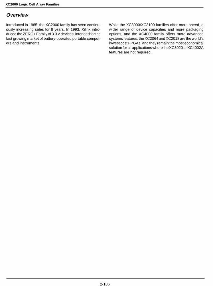
Typ. Logic UserCapacity I/O Config.
Device V CC (gates) CLBs Max bits
XC2064 5.0 V 600 – 1,000 64 58 12,038XC2064L 3.3 V 600 – 1,000 64 58 12,038XC2018 5.0 V 1,000 - 1,500 100 74 17,878XC2018L 3.3 V 1,000 - 1,500 100 74 17,878
The XC2000 family operates with a nominal 5.0 V supply.The XC2000L family operates with nominal 3.3 V supply.
The LCA logic functions and interconnections are deter-mined by data stored in internal static-memory cells. On-chip logic provides for automatic loading of configurationdata at power-up. The program data can reside in anEEPROM, EPROM or ROM on the circuit board or on afloppy disk or hard disk. The program can be loaded in anumber of modes to accommodate various system re-quirements.
Architecture
The general structure of a Logic Cell Array is shown inFigure 1. The elements of the array include three catego-ries of user programmable elements: I/O Blocks (IOBs),Configurable Logic Blocks (CLBs) and ProgrammableInterconnections. The I/OBs provide an interface betweenthe logic array and the device package pins. The CLBsperform user-specified logic functions, and the intercon-nect resources are programmed to form networks thatcarry logic signals among the blocks.
LCA configuration is established through a distributedarray of memory cells.The XACT development systemgenerates the program used to configure the Logic CellArray which includes logic to implement automatic con-figuration.
Configuration MemoryThe configuration of the Logic Cell Array is established byprogramming memory cells which determine the logicfunctions and interconnections. The memory loading pro-cess is independent of the user logic functions.
XC2000Logic Cell Array Families
Product Description
Features
• Fully Field-Programmable:– I/O functions– Digital logic functions– Interconnections
• General-purpose array architecture
• Complete user control of design cycle
• Compatible arrays with logic cell complexity equiva-lent from 600 to 1,500 gates
• Available in 5-V and 3.3-V versions
• 100% factory tested
• Selectable configuration modes
• Low-power, CMOS, static-memory technology
• Performance equivalent to TTL SSI/MSI
• TTL or CMOS input thresholds
• Complete development system support– XACT Design Editor– Schematic Entry– Macro Library– Timing Calculator– Logic and Timing Simulator– Auto Place / Route
Description
The Logic Cell Array (LCA) is a high density CMOSintegrated circuit. Its user-programmable array architec-ture is made up of three types of configurable elements:Input/Output Blocks, logic blocks and Interconnect. Thedesigner can define individual I/O blocks for interface toexternal circuitry, define logic blocks to implement logicfunctions and define interconnection networks to composelarger scale logic functions. The XACT Development Sys-tem provides interactive graphic design capture and auto-matic routing. Both logic simulation and in-circuit emula-tion are available for design verification.
The Logic Cell Array is available in a variety of logiccapacities, package styles, temperature ranges and speedgrades.

XC2000 Logic Cell Array Families
2-188
The static memory cell used for the configuration memoryin the Logic Cell Array has been designed specifically forhigh reliability and noise immunity. Based on this design,which has been patented, integrity of the LCA configura-tion memory is assured even under adverse conditions.Compared with other programming alternatives, staticmemory provides the best combination of high density,high performance, high reliability and comprehensive test-ability. As shown in Figure 2, the basic memory cellconsists of two CMOS inverters plus a pass transistor usedfor writing data to the cell. The cell is only written duringconfiguration and only read during readback. During nor-mal operation the pass transistor is off and does not affectthe stability of the cell. This is quite different from thenormal operation of conventional memory devices, inwhich the cells are continuously read and rewritten.
The outputs Q and Q control pass-transistor gates directly.The absence of sense amplifiers and the output capacitiveload provide additional stability to the cell. Due to thestructure of the configuration memory cells, they are not
affected by extreme power supply excursions or very highlevels of alpha particle radiation. In reliability testing no softerrors have been observed, even in the presence of veryhigh doses of alpha radiation.
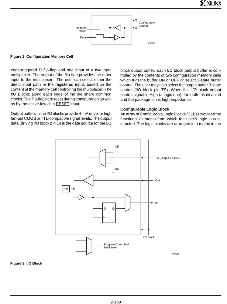
Input/Output BlockEach user-configurable I/O block (IOB) provides an inter-face between the external package pin of the device andthe internal logic. Each I/O block includes a programmableinput path and a programmable output buffer. It alsoprovides input clamping diodes to provide protection fromelectro-static damage, and circuits to protect the LCA fromlatch-up due to input currents. Figure 3 shows the generalstructure of the I/O block.
The input buffer portion of each I/O block provides thresh-old detection to translate external signals applied to thepackage pin to internal logic levels. The input bufferthreshold of the I/O blocks can be programmed to becompatible with either TTL (1.4 V) or CMOS (2.2 V) levels.The buffered input signal drives both the data input of an
Figure 1. Logic Cell Array Structure
Configurable Logic Block
I/O Block
Interconnect Area
X5418
2-189
Figure 2. Configuration Memory Cell
edge-triggered D flip-flop and one input of a two-inputmultiplexer. The output of the flip-flop provides the otherinput to the multiplexer. The user can select either thedirect input path or the registered input, based on thecontent of the memory cell controlling the multiplexer. TheI/O Blocks along each edge of the die share commonclocks. The flip-flops are reset during configuration as wellas by the active-low chip RESET input.
Output buffers in the I/O blocks provide 4-mA drive for highfan-out CMOS or TTL-compatible signal levels. The outputdata (driving I/O block pin O) is the data source for the I/O
block output buffer. Each I/O block output buffer is con-trolled by the contents of two configuration memory cellswhich turn the buffer ON or OFF or select 3-state buffercontrol. The user may also select the output buffer 3-statecontrol (I/O block pin TS). When this I/O block outputcontrol signal is High (a logic one), the buffer is disabledand the package pin is high-impedance.
Configurable Logic BlockAn array of Configurable Logic Blocks (CLBs) provides thefunctional elements from which the user’s logic is con-structed. The logic blocks are arranged in a matrix in the
D Q
Pin
X5398
Off
On
TS (Output Enable)
Out
In
I/O Clock
Program-Controlled Multiplexer
=
Figure 3. I/O Block
Q
Data
Read or Write
Configuration Control
Q
X5382

XC2000 Logic Cell Array Families
2-190
Figure 4. Configurable Logic Block
combinatorial logic (Option 3) is a special case of the 2-function form in which the B input dynamically selectsbetween the two function tables providing a single mergedlogic function output. This dynamic selection allows some5-variable functions to be generated from the four blockinputs and storage element Q. Combinatorial functions arerestricted in that one may not use both its storage elementoutput Q and the input variable of the logic block pin “D” inthe same function.
If used, the storage element in each Configurable LogicBlock (Figure 6) can be programmed to be either an edge-sensitive “D” type flip-flop or a level-sensitive “D” latch. Theclock or enable for each storage element can be selectedfrom:
• The special-purpose clock input K• The general-purpose input C• The combinatorial function G
The user may also select the clock active sense withineach logic block. This programmable inversion eliminatesthe need to route both phases of a clock signal throughoutthe device.
The storage element data input is supplied from thefunction F output of the combinatorial logic. Asynchro-nous SET and RESET controls are provided for eachstorage element. The user may enable these controlsindependently and select their source. They are activeHigh inputs and the asynchronous reset is dominant. The
center of the device. The XC2064 has 64 such blocksarranged in an 8-row by 8-column matrix. The XC2018 has100 logic blocks arranged in a 10 by 10 matrix.
Each logic block has a combinatorial logic section, astorage element, and an internal routing and control sec-tion. Each CLB has four general-purpose inputs: A, B, Cand D; and a special clock input (K), which may be drivenfrom the interconnect adjacent to the block. Each CLB alsohas two outputs, X and Y, which may drive interconnectnetworks. Figure 4 shows the resources of a ConfigurableLogic Block.
The logic block combinatorial logic uses a table look-upmemory to implement Boolean functions. This techniquecan generate any logic function of up to four variables witha high speed sixteen-bit memory. The propagation delaythrough the combinatorial network is independent ofthe function generated. Each block can perform anyfunction of four variables or any two functions of threevariables each. The variables may be selected fromamong the four inputs and the block’s storage elementoutput Q. Figure 5 shows various options which may bespecified for the combinatorial logic.
If the single 4-variable configuration is selected (Option 1),the F and G outputs are identical. If the 2-function alterna-tive is selected (Option 2), logic functions F and G may beindependent functions of three variables each. The threevariables can be selected from among the four logic blockinputs and the storage element output Q. A third form of the
D QS
R
A
B
C
D
Inputs
K Clock
X
Y
Outputs
K
Comb.
Logic
X5399
F
G

2-191
storage elements are reset by the active-Low chip RESETpin as well as by the initialization phase preceding configu-ration. If the storage element is not used, it is disabled.
The two block outputs, X and Y, can be driven by either thecombinatorial functions, F or G, or the storage elementoutput Q (Figure 4). Selection of the outputs is completelyinterchangeable and may be made to optimize routingefficiencies of the networks interconnecting the logic blocksand I/O blocks.
Programmable Interconnect
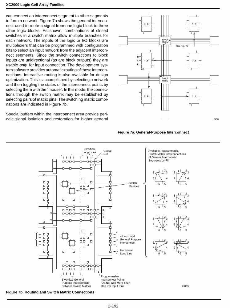
Programmable interconnection resources in the Logic CellArray provide routing paths to connect inputs and outputsof the I/O and logic blocks into desired networks. Allinterconnections are composed of metal segments, withprogrammable switching points provided to implement thenecessary routing. Three types of resources accommo-date different types of networks.
• General purpose interconnect• Longlines• Direct connection
General-Purpose InterconnectGeneral-purpose interconnect, as shown in Figure 7a, iscomposed of four horizontal metal segments between therows and five vertical metal segments between the col-umns of logic and I/O blocks. Each segment is only theheight or width of a logic block. Where these segmentswould cross at the intersections of rows and columns, Figure 6. CLB Storage Elememt
switching matrices are provided to allow interconnectionsof metal segments from the adjoining rows and columns.Switches in the switch matrices and on block outputs arespecially designed transistors, each controlled by a con-figuration bit.
Logic-block output switches provide contacts to adjacentgeneral interconnect segments and therefore to the switch-ing matrix at each end of those segments. A switch matrix
Figure 5. CLB Combinatorial Logic OptionsNote: Variables D and Q can not be used in the same function.
D QSET
RESG
G
F
F
D
C
K
A
X5400
M U X
A
Option 2
2 Functions of 3 Variables
Option 3
Dynamic Selection of 2 Functions of 3
Variables
Q
Q
Q
Q
A
B
C
D
A
B
C
D
G
F
D
A
D
B
F
G
Any Function
of 4 Variables
Option 1
1 Function of 4 Variables
A
B
C
D
Q
F
GC
C
Any Function
of 3 Variables
Any Function
of 3 Variables
Any Function
of 3 Variables
Any Function
of 3 Variables
X5393
XC2000 Logic Cell Array Families
2-192
can connect an interconnect segment to other segmentsto form a network. Figure 7a shows the general intercon-nect used to route a signal from one logic block to threeother logic blocks. As shown, combinations of closedswitches in a switch matrix allow multiple branches foreach network. The inputs of the logic or I/O blocks aremultiplexers that can be programmed with configurationbits to select an input network from the adjacent intercon-nect segments. Since the switch connections to blockinputs are unidirectional (as are block outputs) they areusable only for input connection. The development sys-tem software provides automatic routing of these intercon-nections. Interactive routing is also available for designoptimization. This is accomplished by selecting a networkand then toggling the states of the interconnect points byselecting them with the “mouse”. In this mode, the connec-tions through the switch matrix may be established byselecting pairs of matrix pins. The switching matrix combi-nations are indicated in Figure 7b.
Special buffers within the interconnect area provide peri-odic signal isolation and restoration for higher general
Figure 7b. Routing and Switch Matrix Connections
X
Y
bck
aa
d
4 HorizontalGeneral PurposeInterconnect
HorizontalLong Line
5 Vertical GeneralPurpose InterconnectsBetween Switch Matrics
ProgrammableInterconnect Points(Do Not Use More ThanOne Per Input Pin)
2 VerticalLong Lines Global
Net
SwitchMatrices
1 2
6 5
3
4
8
7
1 2
6 5
3
4
8
7
1 2
6 5
3
4
8
7
1 2
6 5
3
4
8
7
1 2
6 5
3
4
8
7
1 2
6 5
3
4
8
7
1 2
6 5
3
4
8
7
1 2
6 5
3
4
8
7
Available ProgrammableSwitch Matrix Interconnectionsof General InterconnectSegments by Pin
X3175
d
CLB
B
C
K
D
A
X
Y
CLB
CLB
CLB
CLB
CLB
Switch Matrix
Switch Matrix
See Fig. 7b
X5401
Figure 7a. General-Purpose Interconnect

2-193
interconnect fan-out and better performance. The repow-ering buffers are bidirectional, since signals must be ableto propagate in either direction on a general interconnectsegment. Direction controls are automatically establishedby the Logic Cell Array development system software.Repowering buffers are provided only for the general-purpose interconnect since the direct and Longline re-sources do not exhibit the same R-C delay accumulation.The Logic Cell Array is divided into nine sections withbuffers automatically provided for general interconnect atthe boundaries of these sections. These boundaries canbe viewed with the development system. For routingwithin a section, no buffers are used. The delay calculatorof the XACT development system automatically calculatesand displays the block, interconnect and buffer delays forany selected paths.
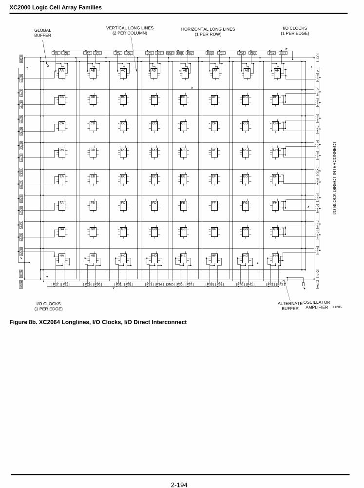
LonglinesLonglines, shown in Figure 8a, run both vertically andhorizontally the height or width of the interconnect area.Each vertical interconnection column has two Longlines;each horizontal row has one, with an additional Longlineadjacent to each set of I/O blocks. The Longlines bypassthe switch matrices and are intended primarily for signals
that must travel a long distance or must have minimumskew among multiple destinations.
A global buffer in the Logic Cell Array is available to drivea single signal to all B and K inputs of logic blocks. Usingthe global buffer for a clock provides a very low skew, highfan-out synchronized clock for use at any or all of the logicblocks. At each block, a configuration bit for the K input tothe block can select this global line as the storage elementclock signal. Alternatively, other clock sources can beused.
A second buffer below the bottom row of the array drivesa horizontal Longline which, in turn, can drive a verticalLongline in each interconnection column. This alternatebuffer also has low skew and high fan-out capability. Thenetwork formed by this alternate buffer’s Longlines can beselected to drive the B, C or K inputs of the logic blocks.
Alternatively, these Longlines can be driven by a logic orI/O block on a column by column basis. This capabilityprovides a common, low-skew clock or control line withineach column of logic blocks. Interconnections of theseLonglines are shown in Figure 8b.
Figure 8a. Longline Interconnect
CLB
B
C
K
D
A
X
Y
CLB
CLB
CLB
CLB
CLB
Switch Matrix
Switch Matrix
X5402
Global Long Lines
Two Vertical Long Lines
Horizontal Long Lines
XC2000 Logic Cell Array Families
2-194
AA AB AC AD AE AF AG AH
BA BB BC BD BE BF BG BH
CA CB CC CD CE CF CG CH
DA DB DC DD DE DF DG DH
EA EB EC ED EE EF EG EH
FA FB FC FD FF FG FH
GA GB GC GD GE GF GG GH
I/O B
LOC
K D
IRE
CT
INT
ER
CO
NN
EC
T
HA HB HC HD HE HF HG HH
P9 P8 P7 P6 P5 P4 P3 P2 P68GND P67 P66 P65 P64 P63 P62 P61
FE
P27 P28 P29 P30 P31 P32 P33 P34 P36 P37 P38 P39 P40 P41 P42 P43GND
P 5 9
C C L
P 5 8
P 5 7
P 5 6
P 5 4
P 5 3
V C C
P 5 1
P 5 0
P 4 9
P 4 7
P 4 8
P 4 6
O P
R S T
M 1 R
M 0 R
P 5 5
HORIZONTAL LONG LINES (1 PER ROW)
I/O CLOCKS (1 PER EDGE)
P 2 4
P 2 3
P 2 2
P 2 1
P 2 0
P 1 9
V C C
P 1 7
P 1 6
P 1 5
P 1 4
P 1 3
P 1 2
P 1 1
P W R
GLOBAL BUFFER
VERTICAL LONG LINES (2 PER COLUMN)
OSCILLATOR AMPLIFIER
ALTERNATE BUFFER
I/O CLOCKS (1 PER EDGE) X1205
Figure 8b. XC2064 Longlines, I/O Clocks, I/O Direct Interconnect

2-195
Direct InterconnectDirect interconnect, shown in Figure 9, provides the mostefficient implementation of networks between adjacentlogic or I/O blocks. Signals routed from block to block bymeans of direct interconnect exhibit minimum intercon-nect propagation and use minimum interconnect re-sources. For each Configurable Logic Block, the X outputmay be connected directly to the C or D inputs of the CLBabove and to the A or B inputs of the CLB below it. The Youtput can use direct interconnect to drive the B input of theblock immediately to its right. Where logic blocks areadjacent to I/O blocks, direct connect is provided to theI/O block input (I) on the left edge of the die, the output (O)on the right edge, or both on I/O blocks at the top andbottom of the die. Direct interconnections of I/O blocks withCLBs are shown in Figure 8b.
Crystal Oscillator
Figure 8b also shows the location of an internal high speedinverting amplifier which may be used to implement an on-chip crystal oscillator. It is associated with the auxiliarybuffer in the lower right corner of the die. When theoscillator is configured by MAKEBITS and connected as asignal source, two special user IOBs are also configured toconnect the oscillator amplifier with external crystal oscil-lator components as shown in Figure10. The oscillatorcircuit becomes active early in the configuration process inorder to allow the oscillator to stabilize. Actual internalconnection is delayed until completion of configuration. InFigure 10, the feedback resistor R1, between the outputand input, biases the amplifier at threshold. The inversionof the amplifier, together with the R-C networks and an AT-cut series resonant crystal, produce the 360-degree phaseshift of the Pierce oscillator. A series resistor R2 may beincluded to add to the amplifier output impedance whenneeded for phase-shift control, crystal resistance match-ing, or to limit the amplifier input swing to control clippingat large amplitudes. Excess feedback voltage may becorrected by the ratio of C2/C1. The amplifier is designedto be used from 1 MHz to about one-half the specified CLBtoggle frequency. Use at frequencies below 1 MHz mayrequire individual characterization with respect to a seriesresistance. Crystal oscillators above 20 MHz generallyrequire a crystal which operates in a third overtone mode,where the fundamental frequency must be suppressed byan inductor across C2, turning this parallel resonant circuitto double the fundamental crystal frequency, i.e., 2/3 of thedesired third harmonic frequency network. When the oscil-lator inverter is not used, these IOBs and their packagepins are available for general user I/O.
CLB
B
C
K
D
A
X
Y
CLB
CLB
CLB
CLB
CLB
Switch Matrix
Switch Matrix
X5403
Direct Interconnect
Figure 10. Crystal Oscillator
Figure 9. Direct Interconnect
ExternalOn-ChipAlternate
Clock Buffer
XTAL2 (IN)
R1
R2
XTAL1
Y1C1 C2
Suggested Component Values R1 R2 C1, C2 Y1
0.5 - 1 MΩ 0 - 1 kΩ (may be required for low frequency, phase shift and/or compensation level for crystal Q) 10 - 40 pF 1 - 20 MHz AT cut series resonant
48 DIP 68 PLCC 68 PGA 84 PLCC 84 PGA
XTAL2 30 43 L10 53 L11
XTAL1 33 46 J10 56
K11
X5404

XC2000 Logic Cell Array Families
2-196
Programming
Table 1. Configuration Mode Selection
M0 M1 M2 CCLK Mode Data
0 0 0 output Master Bit Serial0 0 1 output Master Byte Wide Addr. = 0000 up0 1 0 — reserved —0 1 1 output Master Byte Wide Addr. = FFFF
down1 0 0 — reserved —1 0 1 output Peripheral Bit Serial1 1 0 — reserved —1 1 1 input Slave Bit Serial
Configuration data to define the function and intercon-nection within a Logic Cell Array are loaded automaticallyat power-up or upon command. Several methods of auto-matically loading the required data are designed into theLogic Cell Array and are determined by logic levels appliedto mode selection pins at configuration time. The form ofthe data may be either serial or parallel, depending on theconfiguration mode. The programming data are indepen-dent of the configuration mode selected. The state dia-gram of Figure 11 illustrates the configuration process.Input thresholds for user I/O pins can be selected to beeither TTL-compatible or CMOS-compatible. At power-up,all inputs are TTL-compatible and remain in that state untilthe LCA begins operation. If the user has selected CMOScompatibility, the input thresholds are changed to CMOSlevels during configuration.
Figure 12 shows the specific data arrangement for theXC2064 device. Future products will use the same dataformat to maintain compatibility between different devicesof the Xilinx product line, but they will have different sizesand numbers of data frames. For the XC2064, configura-tion requires 12,038 bits for each device. For the XC2018,the configuration of each device requires 17,878 bits. TheXC2064 uses 160 configuration data frames and theXC2018 uses 197.
The configuration bit stream begins with preamble bits, apreamble code and a length count. The length count isloaded into the control logic of the Logic Cell Array and isused to determine the completion of the configurationprocess. When configuration is initiated, a 24-bit lengthcounter is set to 0 and begins to count the total number ofconfiguration clock cycles applied to the device. When thecurrent length count equals the loaded length count, theconfiguration process is complete. Two clocks beforecompletion, the internal logic becomes active and is reset.On the next clock, the inputs and outputs become active asconfigured and consideration should be given to avoidconfiguration signal contention. (Attention must be paid toavoid contention on pins which are used as inputs duringconfiguration and become outputs in operation.) On thelast configuration clock, the completion of configuration is
signalled by the release of the DONE / PROG pin of thedevice as the device begins operation. This open-drainoutput can be AND-tied with multiple Logic Cell Arrays andused as an active-High READY or active-Low , RESET, toother portions of the system. High during configuration(HDC) and low during configuration (LDC), are releasedone CCLK cycle before DONE is asserted. In master modeconfigurations, it is convenient to use LDC as an active-Low EPROM chip enable.
As each data bit is supplied to the LCA, it is internallyassembled into a data word. As each data word is com-pletely assembled, it is loaded in parallel into one word ofthe internal configuration memory array. The last wordmust be loaded before the current length count compare istrue. If the configuration data are in error, e.g., PROMaddress lines swapped, the LCA will not be ready at thelength count and the counter will cycle through an addi-tional complete count prior to configuration being “done”.
Table 1 shows the selection of the configuration modebased on the state of the mode pins M0 and M1. Thesepackage pins are sampled prior to the start of the configu-ration process to determine the mode to be used. Onceconfiguration is DONE and subsequent operation hasbegun, the mode pins may be used to perform datareadback, as discussed later. An additional mode pin,M2, must be defined at the start of configuration. Thispackage pin is a user-configurable I/O after configurationis complete.
Initialization PhaseWhen power is applied, an internal power-on-reset circuitis triggered. When Vcc reaches the voltage at which theLCA device begins to operate (nominally 2.5 to 3 V), thechip is initialized, outputs are made high-impedance and atime-out is initiated to allow time for power to stabilize. Thistime-out (11 to 33 ms) is determined by a counter driven bya self-generated, internal sampling clock that drives theconfiguration clock (CCLK) in master configuration mode.This internal sampling clock will vary with process, tem-perature and power supply over the range of 0.5 to 1.5MHz. LCA devices with mode lines set for master modewill time-out of their initialization using a longer counter (43to 130 ms) to assure that all devices, which it may bedriving in a daisy chain, will be ready. Configuration usingperipheral or slave modes must be delayed long enoughfor this initialization to be completed.
The initialization phase may be extended by asserting theactive-Low external RESET. If a configuration has begun,an assertion of RESET will initiate an abort, including anorderly clearing of partially loaded configuration memorybits. After about three clock cycles for synchronization,initialization will require about 160 additional cycles of theinternal sampling clock (197 for the XC2018) to clear theinternal memory before another configuration may begin.

2-197
Power-On Delay is 214 Cycles for Non-Master Mode—11 to 33 ms 216 Cycles for Master Mode—43 to 130 ms
InitializationTest M0
Power-On Delay
ClearConfiguration
Memory
RESETActive
TestMode Pins
ConfigurationProgram Mode Start-Up Operational
Mode
PWRDWNInactive
PWRDWNActive
Power DownNo HDC, LDC
or Pull-Up
Active RESET Operates on User Logic
Low on DONE/PROGRAM and RESET
No
X5307
Active RESET
Yes
User I/O Pins 3-Stated with High Impedance Pull-Up, HDC=High, LDC=Low
Clear Is ~ 160 Cycles for the XC2064—100 to 320 µs ~ 200 Cycles for the XC2018—125 to 390 µs
Figure 12. XC2064 Internal Configuration Data Arrangement
Reprogramming is initialized by a High-to-Low transitionon RESET (after RESET has been High for at least 6 µs)followed by a Low level (for at least 6 µs) on both theRESET and the open-drain DONE/PROG pins. This re-turns the LCA device to the CLEAR state, as shown inFigure 11.
Master ModeIn Master mode, the Logic Cell Array automatically loadsthe configuration program from an external memory de-vice. The Master Serial mode uses serial configurationdata, synchronized by the rising edge of CCLK, as shownin Figure 13.
In Master Parallel mode (Figure 14), the Logic Cell Arrayprovides 16 address outputs and the control signals RCLK(Read Clock), HDC (High during configuration) and LDC(Low during configuration) to execute Read cycles fromthe external memory. Parallel 8-bit data words are readand internally serialized. As each data word is read, theleast significant bit of each byte, normally D0, is the next bitin the serial stream.
Addresses supplied by the Logic Cell Array can be se-lected by the mode lines to begin at address 0 andincremented to reach the memory (master Low mode), orthey can begin at address FFFF Hex and be decremented
Figure 11. A State Diagram of the Configuration Process for Power-up and Reprogram
11111111 0010 <24-Bit Length Count> 1111 0 <Data Frame # 001> 111 0 <Data Frame # 002> 111 0 <Data Frame # 003> 111 . . . . . . . . . . . . 0 <Data Frame # 159> 111 0 <Data Frame # 160> 111 1111
Dummy Bits (4 Bits Minimum), XACT 2.10 Generates 8 Bits Preamble Code Configuration Program Length Dummy Bits (4 Bits Minimum)
Configuration Frames Data Bits Per Frame Postamble Code (4 Bits Minimum)
XC2064
160
71
XC2018
196
87
Program Data Repeated for Each Logic Cell Array in a Daisy Chain
Header
Start-Up Requires Three Configuration Clocks Beyond Length Count X5405
XC2000 Logic Cell Array Families
2-198
Daisy ChainThe daisy-chain programming mode is supported by LogicCell Arrays in all programming modes. In master mode andperipheral modes, the LCA device can act as a source ofdata and control for slave devices. For example, Figure 14shows a single device in master mode, with two devices inslave mode. The master-mode device reads the externalmemory and begins the configuration loading process forall of the devices.
The data begins with a preamble and a length count whichare supplied to all devices at the beginning of the configu-ration. The length count represents the total number ofcycles required to load all of the devices in the daisy chain.After loading the length count, the lead device will load itsconfiguration data while providing a High DOUT to down-stream devices. When the lead device has been loadedand the current length count has not reached the full value,memory access continues. Data bytes are read and seri-alized by the lead device. The data is passed through thelead device and appears on the data out (DOUT) pin inserial form. The lead device also generates the configura-tion clock (CCLK) to synchronize the serial output data. Amaster-mode device generates an internal CCLK of eighttimes the EPROM address rate, while a peripheral modedevice produces CCLK from the chip select and writestrobe timing.
OperationWhen all of the devices have been loaded and the lengthcount is complete, a synchronous start-up of operation isperformed. On the clock cycle following the end of loading,the internal logic begins functioning in the reset state. Onthe next CCLK, the configured output buffers becomeactive to allow signals to stabilize. The next CCLK cycleproduces the DONE condition. The length count control ofoperation allows a system of multiple Logic Cell Arrays tobegin operation in a synchronized fashion. If the crystaloscillator is used, it will begin operation before configura-tion is complete to allow time for stabilization before it isconnected to the internal circuitry.
ReprogramThe Logic Cell Array configuration memory may be re-written while the device is operating in the user’s system.The LCA device returns to the Clear state where theconfiguration memory is cleared, I/O pins disabled, andmode lines re-sampled. Reprogram control is often imple-mented using an external open collector driver which pullsDONE/PROG LOW. Once it recognizes a stable request,the Logic Cell Array holds DONE/PROG LOW until thenew configuration has been completed. Even if the DONE/PROG pin is externally held LOW beyond the configura-tion period, the Logic Cell Array begins operation uponcompletion of configuration. To reduce sensitivity to noise,these re-program signals are filtered for 2–3 cycles of the
(master High mode). This capability is provided to allowthe Logic Cell Array to share external memory with anotherdevice, such as a microprocessor. For example, if theprocessor begins its execution from Low memory, theLogic Cell Array can load itself from High memory andenable the processor to begin execution once configura-tion is completed. The Done/PROG output pin can be usedto hold the processor in a Reset state until the Logic CellArray has completed the configuration process
Peripheral Mode (Bit Serial)Peripheral mode provides a simplified interface throughwhich the device may be loaded as a processor peripheral.Figure 15 shows the peripheral mode connections. Pro-cessor Write cycles are decoded from the common asser-tion of the active-Low write strobe (IOWRT), and twoactive-Low and of the active-High chip selects (CS0 CS1CS2). If all these signals are not available, the unusedinputs should be driven to their respective active levels.The Logic Cell Array will accept one bit of the configurationprogram on the data input (DIN) pin for each processorWrite cycle. Data is supplied in the serial sequence de-scribed earlier.
Since only a single bit from the processor data bus isloaded per cycle, the loading process involves the proces-sor reading a byte or word of data, writing a bit of the datato the Logic cell Array, shifting the word and writing a bituntil all bits of the word are written, then continuing in thesame fashion with the next word, etc. After the configura-tion program has been loaded, an additional three clocks(a total of three more than the length count) must besupplied in order to complete the configuration process.When more than one device is being used in the system,each device can be assigned a different bit in the proces-sor data bus, and multiple devices can be loaded on eachprocessor write cycle. This broadside loading methodprovides a very easy and time-efficient method of loadingseveral devices.
Slave ModeSlave mode, Figure 16, provides the simplest interface forloading the Logic Cell Array configuration. Data is suppliedin conjunction with a synchronizing clock. For each Low-to-High input transition of configuration clock (CCLK), thedata present on the data input (DIN) pin is loaded into theinternal shift register. Data may be supplied by a processoror by other special circuits. Slave mode is used for down-stream devices in a daisy-chain configuration. The datafor each slave LCA device are supplied by the precedingLCA device in the chain, and the clock is supplied by thelead device, which is configured in master or peripheralmode. After the configuration program has been loaded,an additional three clocks (a total of three more than thelength count) must be supplied in order to complete theconfiguration process.

2-199
LCA internal timing generator (2 to 6 µs). Note that theClear time-out for a master-mode reprogram or abort doesnot have the 4 times delay of the Initialization state. If adaisy chain is used, an external RESET is required, longenough to guarantee clearing all non-master mode de-vices. For XC2000-series LCA devices, this is accom-plished with an external time delay.
In some applications the system power supply might havemomentary failures which can leave the LCA control logicin an invalid state. There are two methods to recover fromthis state. The first is to cycle the VCC supply to less than0.1 V and re-apply valid VCC. The second is to provide theLCA device with simultaneous Low levels of at least 6 µson RESET and DONE/PROG pins after the RESET pinhas been High following a return to valid VCC. This guaran-tees that the LCA device will return to the Clear state.Either of these methods may be needed in the event of anincomplete voltage interruption. They are not needed for anormal application of power from an off condition.
Battery BackupBecause the control store of the Logic Cell Array is aCMOS static memory, its cells require only a very lowstandby current for data retention. In some systems, thislow data-retention current characteristic facilitates pre-serving configurations in the event of a primary power loss.The Logic Cell Array has built in power-down logic which,when activated, clears all internal flip-flops and latches,but retains the configuration. All outputs are placed in thehigh-impedance state, and all input levels are ignored. Theinternal logic considers all inputs to be ones (High). Con-figuration is not possible during power down.
Power-down data retention is possible with a simple bat-tery-backup circuit because the power requirement isextremely low. For retention at 2.0 V, the required currentis typically on the order of 500 nA. Screening to thisparameter is available. To force the Logic Cell Array intothe power-down state, the user must pull the PWRDWNpin Low and continue to supply a retention voltage to theVCC pins of the package. When normal power is restored,VCC is elevated to its normal operating voltage andPWRDWN is returned to a High. The Logic Cell Arrayresumes operation with the same internal sequence thatoccurs at the conclusion of configuration. Internal I/O andlogic block storage elements will be reset, the outputs willbecome enabled and then the DONE/PROG pin will bereleased. No configuration programming is involved.
Special Configuration Functions
In addition to the normal user logic functions and inter-connect, the configuration data include control for severalspecial functions:
• Input thresholds• Readback disable• DONE pull-up resistor
Each of these functions is controlled by a portion of theconfiguration program generated by the XACT Develop-ment System.
Input ThresholdsDuring configuration, all input thresholds are TTL level.After configuration, input thresholds are establishedas specified, either TTL or CMOS. The PWRDWN inputthreshold is an exception; it is always a CMOS level input.The TTL threshold option requires additional power forthreshold shifting.
ReadbackAfter a Logic Cell Array has been programmed, the con-figuration program may be read back from the device.Readback may be used for verification of configuration,and as a method of determining the state of internal logicnodes during debugging. Three Readback options areprovided: on command, only once, and never.
An initiation of Readback is produced by a Low-to-Hightransition of the M0 / RTRIG (Read Trigger) pin. The CCLKinput must then be driven by external logic to read back theconfiguration data. The first three Low-to-High CCLKtransitions clock out dummy data. The subsequent Low-to-High CCLK transitions shift the data frame informationout on the M1/RDATA (Read Data) pin. Note that the logicpolarity is always inverted, a zero in Configuration be-comes a one in Readback, and vice versa. Note also thateach Readback frame has one Start bit (read back as aone) but, unlike in Configuration, each Readback framehas only one Stop bit (read back as a zero). The thirdleading dummy bit mentioned above can be consideredthe Start bit of the first frame.
All data frames must be read back to complete the processand return the Mode Select and CCLK pins to their normalfunctions. Readback data includes the state of all internalstorage elements. This information is used by the XACTdevelopment system In-Circuit Debugger to provide visi-bility into the internal operation of the logic while thesystem is operating. To read back a uniform time sampleof all storage elements, it may be necessary to inhibit thesystem clock.
DONE Pull-upThe DONE / PROG pin is an open drain I/O that indicatesprogramming status. As an input, it initiates a reprogramoperation. An optional internal pull-up resistor may beenabled.
The following seven pages describe the four configurationmodes in detail.
XC2000 Logic Cell Array Families
2-200
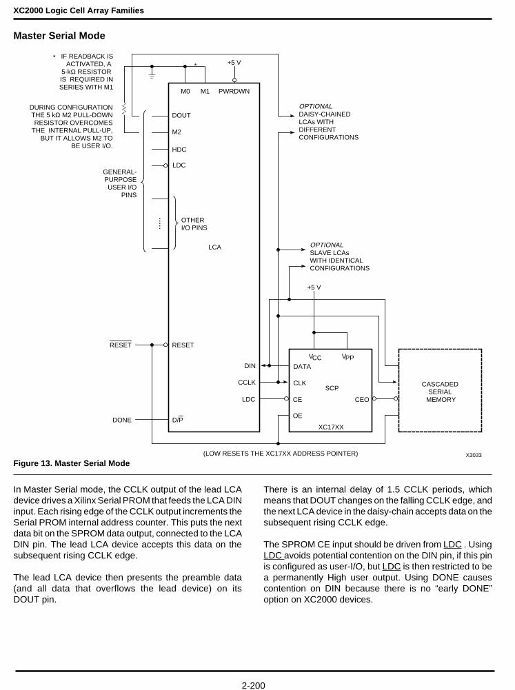
Master Serial Mode
Figure 13. Master Serial Mode
In Master Serial mode, the CCLK output of the lead LCAdevice drives a Xilinx Serial PROM that feeds the LCA DINinput. Each rising edge of the CCLK output increments theSerial PROM internal address counter. This puts the nextdata bit on the SPROM data output, connected to the LCADIN pin. The lead LCA device accepts this data on thesubsequent rising CCLK edge.
The lead LCA device then presents the preamble data(and all data that overflows the lead device) on itsDOUT pin.
There is an internal delay of 1.5 CCLK periods, whichmeans that DOUT changes on the falling CCLK edge, andthe next LCA device in the daisy-chain accepts data on thesubsequent rising CCLK edge.
The SPROM CE input should be driven from LDC . UsingLDC avoids potential contention on the DIN pin, if this pinis configured as user-I/O, but LDC is then restricted to bea permanently High user output. Using DONE causescontention on DIN because there is no “early DONE”option on XC2000 devices.
X3033
CE
GENERAL-PURPOSEUSER I/O
PINS
M0 M1 PWRDWN
DOUT
M2
HDC
OTHERI/O PINS
RESET
DIN
CCLK
DATA
CLK
+5 V
.....
OE
LCA
LDC
SCP
CEO
CASCADEDSERIAL
MEMORY
LDC
XC17XX
RESET
SLAVE LCAs WITH IDENTICALCONFIGURATIONS
DURING CONFIGURATIONTHE 5 kΩ M2 PULL-DOWNRESISTOR OVERCOMES
THE INTERNAL PULL-UP,BUT IT ALLOWS M2 TO
BE USER I/O.
(LOW RESETS THE XC17XX ADDRESS POINTER)
OPTIONAL
VCC VPP
+5 V
DAISY-CHAINEDLCAs WITHDIFFERENT CONFIGURATIONS
OPTIONAL
IF READBACK ISACTIVATED, A
5-kΩ RESISTOR IS REQUIRED INSERIES WITH M1
**
DONE D/P
2-201
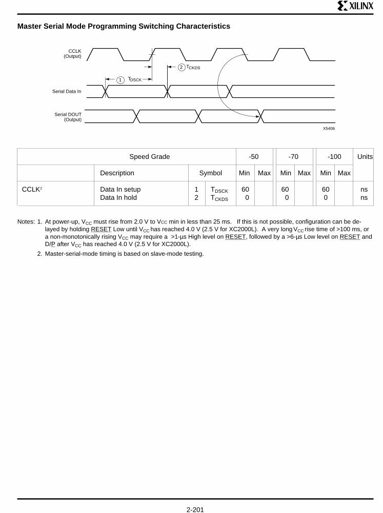
Speed Grade -50 -70 -100 Units
Description Symbol Min Max Min Max Min Max
CCLK2 Data In setup 1 TDSCK 60 60 60 nsData In hold 2 TCKDS 0 0 0 ns
Notes: 1. At power-up, VCC must rise from 2.0 V to VCC min in less than 25 ms. If this is not possible, configuration can be de-layed by holding RESET Low until VCC has reached 4.0 V (2.5 V for XC2000L). A very long VCC rise time of >100 ms, ora non-monotonically rising VCC may require a >1-µs High level on RESET, followed by a >6-µs Low level on RESET andD/P after VCC has reached 4.0 V (2.5 V for XC2000L).
2. Master-serial-mode timing is based on slave-mode testing.
Master Serial Mode Programming Switching Characteristics
Serial Data In
CCLK (Output)
Serial DOUT (Output)
1 TDSCK
2 TCKDS
X5406

XC2000 Logic Cell Array Families
2-202
Master Parallel Mode
Figure 14. Master Parallel Mode Configuration with Daisy Chained Slave Mode Devices. All are configured from the commonEPROM source. A well defined termination of SYSTEM RESET is needed when controlling multiple LCA devices.
In Master Parallel mode, the lead LCA device directlyaddresses an industry-standard byte-wide EPROM andaccepts eight data bits right before incrementing (ordecrementing) the address outputs.
The eight data bits are serialized in the lead LCA device,which then presents the preamble data (and all data thatoverflows the lead device) on the DOUT pin. There is aninternal delay of 1.5 CCLK periods, after the rising CCLKedge that accepts a byte of data, and also changes the
EPROM address, until the falling CCLK edge that makesthe LSB (D0) of this byte appear at DOUT. This means thatDOUT changes on the falling CCLK edge, and the nextLCA device in the daisy-chain accepts data on the subse-quent rising CCLK edge.
Any XC3000 slave driven by an XC2000 master modedevice must use early DONE and early internal reset.(The XC2000 master will not supply the extra clock re-quired by a late programmed XC3000.)
RCLKGeneral- Purpose User I/O
Pins
M0 M1 PWRDWN
M2
HDC
Other I/O Pins
D7
D6
D5
D4
D3
D2
D1
D0
A15
A14
A13
A12
A11
A10
A9
A8
A7
A6
A5
A4
A3
A2
A1
A0
A10
A9
A8
A7
A6
A5
A4
A3
A2
A1
A0
D7
D6
D5
D4
D3
D2
D1
D0
+5 V
• • • • •
CE
OE
LCA
CCLK
DOUT
SYSTEM RESET
A11
A12
A13
A14
A15
EPROM
RESET
• • •
Other I/O Pins
DOUT
M2
HDC
LDC
LCA Slave #1
5 kΩ
M0 M1 PWRDWN
CCLK
DIN
D/P
RESET
DOUT
LCA Slave #n
+5 V
M0 M1 PWRDWN
CCLK
DIN
D/P
General- Purpose User I/O Pins
RESET
Master
• • •
+5 V
8
LDC
• • •
M2
HDC
LDC General- Purpose User I/O Pins
+5 V
D/P
Other I/O Pins
NOTE: Reset of a master device should be asserted by an external timing circuit to allow for LCA CCLK variations in clear state time.
Open CollectorREPROGRAM
5 kΩ
*
If readback is activated, a 5 kΩ resistor is required in series with M1
*
**
5 kΩ5 kΩ
X5407
+5 V
2-203
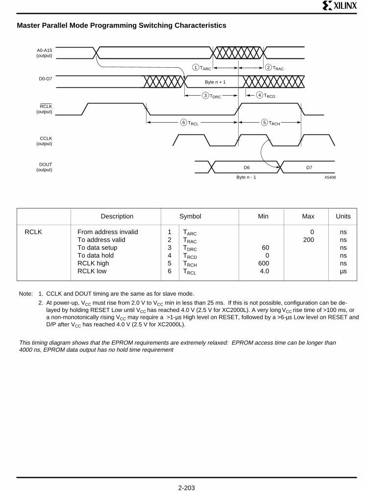
Master Parallel Mode Programming Switching Characteristics
Description Symbol Min Max Units
RCLK From address invalid 1 TARC 0 nsTo address valid 2 TRAC 200 nsTo data setup 3 TDRC 60 nsTo data hold 4 TRCD 0 nsRCLK high 5 TRCH 600 nsRCLK low 6 TRCL 4.0 µs
Note: 1. CCLK and DOUT timing are the same as for slave mode.
2. At power-up, VCC must rise from 2.0 V to VCC min in less than 25 ms. If this is not possible, configuration can be de-layed by holding RESET Low until VCC has reached 4.0 V (2.5 V for XC2000L). A very long VCC rise time of >100 ms, ora non-monotonically rising VCC may require a >1-µs High level on RESET, followed by a >6-µs Low level on RESET andD/P after VCC has reached 4.0 V (2.5 V for XC2000L).
This timing diagram shows that the EPROM requirements are extremely relaxed: EPROM access time can be longer than4000 ns, EPROM data output has no hold time requirement
Byte n + 1
3 TDRC
D7D6
A0-A15 (output)
D0-D7
RCLK (output)
CCLK (output)
DOUT (output)
1 TARC
4 TRCD
Byte n - 1 X5408
2 TRAC
6 TRCL 5 TRCH

XC2000 Logic Cell Array Families
2-204
Peripheral Mode
Figure 15. Peripheral Mode. Configuration data is loaded using serialized data from a microprocessor.
Peripheral mode uses the trailing edge of the logic ANDcondition of the CS0, CS1, CS2, and WRT inputs to acceptbit-serial data from a microprocessor bus. In the lead LCA
device, this data is serially shifted into the internal logic.The lead LCA device presents the preamble data (and alldata that overflows the lead device) on the DOUT pin.
X5397
ADDRESS BUS
DATA BUS
D0
ADDRESS DECODE
LOGIC
CS0...
RESET
...OTHER I/O PINS
DIN CCLK
DOUT
M2
HDC
LDCLCA
GENERAL- PURPOSE USER I/O PINS
D/P
M0 M1 PWR DWN
+5 V
CS2
CS1
5 k½
* IF READBACK IS ACTIVATED, A 5-k½ RESISTOR IS REQUIRED IN SERIES WITH M1
*
OPTIONALDAISY-CHAINED LCAs WITH DIFFERENT CONFIGURATIONS
IOWRT WRT
DONE
RESET

2-205
Peripheral Mode Programming Switching Characteristics
3 TCCC
2 TCI1 TCA
4 TDC
3 TCCC
5 TCD
CSO
CS1
WRT
CS2
CCLK OUTPUT
DIN
DOUT (2) (OUTPUT)
X5384
Description Symbol Min Max Units
Controls1 Active (last active 1 TCA 0.25 5.0 µs(CS0, CS1, input to first inactive)CS2, WRT)
Inactive (first inactive 2 TCI 0.25 µsinput to last active)
CCLK2 3 TCCC 75 nsDIN setup 4 TDC 50 nsDIN hold 5 TCD 0 ns
Notes: 1. Peripheral mode timing determined from last control signal of the logical AND of (CS0, CS1, CS2, WRT) to transition toactive or inactive state.
2. CCLK and DOUT timing are the same as for slave mode.
3. At power-up, VCC must rise from 2.0 V to VCC min in less than 25 ms. If this is not possible, configuration can be de-layed by holding RESET Low until VCC has reached 4.0 V (2.5 V for XC2000L). A very long VCC rise time of >100 ms, or anon-monotonically rising VCC may require a >1-µs High level on RESET, followed by a >6-µs Low level on RESET andD/P after VCC has reached 4.0 V (2.5 V for XC2000L).
XC2000 Logic Cell Array Families
2-206
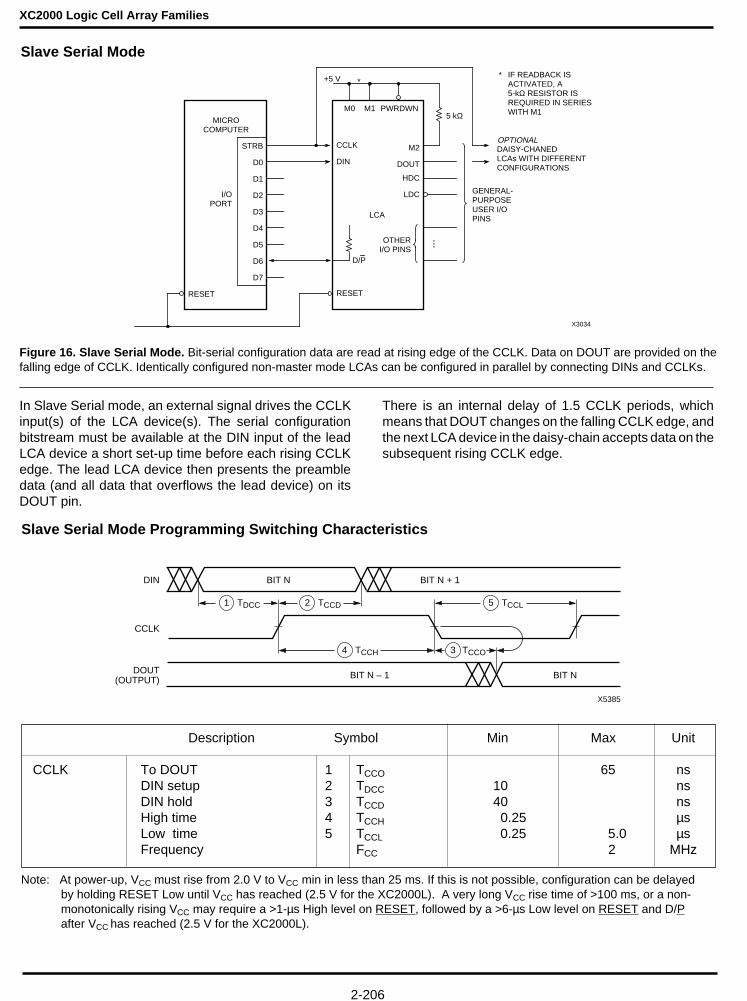
Slave Serial Mode
Figure 16. Slave Serial Mode. Bit-serial configuration data are read at rising edge of the CCLK. Data on DOUT are provided on thefalling edge of CCLK. Identically configured non-master mode LCAs can be configured in parallel by connecting DINs and CCLKs.
In Slave Serial mode, an external signal drives the CCLKinput(s) of the LCA device(s). The serial configurationbitstream must be available at the DIN input of the leadLCA device a short set-up time before each rising CCLKedge. The lead LCA device then presents the preambledata (and all data that overflows the lead device) on itsDOUT pin.
There is an internal delay of 1.5 CCLK periods, whichmeans that DOUT changes on the falling CCLK edge, andthe next LCA device in the daisy-chain accepts data on thesubsequent rising CCLK edge.
Description Symbol Min Max Unit
CCLK To DOUT 1 TCCO 65 nsDIN setup 2 TDCC 10 nsDIN hold 3 TCCD 40 nsHigh time 4 TCCH 0.25 µsLow time 5 TCCL 0.25 5.0 µsFrequency FCC 2 MHz
Note: At power-up, VCC must rise from 2.0 V to VCC min in less than 25 ms. If this is not possible, configuration can be delayedby holding RESET Low until VCC has reached (2.5 V for the XC2000L). A very long VCC rise time of >100 ms, or a non-monotonically rising VCC may require a >1-µs High level on RESET, followed by a >6-µs Low level on RESET and D/Pafter VCC has reached (2.5 V for the XC2000L).
Slave Serial Mode Programming Switching Characteristics
4 TCCH
2 TCCD1 TDCC 5 TCCL
3 TCCO
DIN
CCLK
DOUT (OUTPUT) BIT NBIT N – 1
BIT N BIT N + 1
X5385
D/P
RESET
LCA
GENERAL- PURPOSE USER I/O PINS
+5 V
M0 M1 PWRDWN
CCLK
DIN
STRB
D0
D1
D2
D3
D4
D5
D6
D7
RESET
I/O PORT
MICRO COMPUTER
DOUT
HDC
LDC
M2
*
...OTHER I/O PINS
5 kΩ
OPTIONALDAISY-CHANED LCAs WITH DIFFERENT CONFIGURATIONS
* IF READBACK IS ACTIVATED, A 5-kΩ RESISTOR IS REQUIRED IN SERIES WITH M1
X3034

2-207
Program Readback Switching Characteristics
RTRIG
CCLK(1)
RDATA(Output)
DONE/PROG(Output)
Valid
DRTT RTHT11 12
RTCCT13
CCRDT14
X3168
Description Symbol Min Max Units
RTRIG PROG setup 11 TDRT 300 nsRTRIG high 12 TRTH 250 ns
CCLK RTRIG setup 13 TRTCC 100 nsRDATA delay 14 TCCRD 100 ns
Notes: 1. CCLK and DOUT timing are the same as for slave mode, but TCCL for XC2000L is 0.5 µs min.
2. DONE/PROG output/input must be HIGH (device programmed) prior to a positive transition of RTRIG (M0).
XC2000 Logic Cell Array Families
2-208
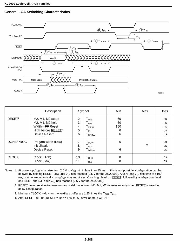
General LCA Switching Characteristics
Notes: 1. At power-up, VCC must rise from 2.0 V to VCC min in less than 25 ms. If this is not possible, configuration can bedelayed by holding RESET Low until VCC has reached (2.5 V for the XC2000L). A very long VCC rise time of >100ms, or a non-monotonically rising VCC may require a >1-µs High level on RESET, followed by a >6-µs Low levelon RESET and D/P after VCC has reached (2.5 V for the XC2000L).
2. RESET timing relative to power-on and valid mode lines (M0, M1, M2) is relevant only when RESET is used todelay configuration.
3. Minimum CLOCK widths for the auxillary buffer are 1.25 times the TCLH, TCLL.
4. After RESET is High, RESET = D/P = Low for 6 µs will abort to CLEAR.
Description Symbol Min Max Units
RESET2 M2, M1, M0 setup 2 TMR 60 nsM2, M1, M0 hold 3 TRM 60 nsWidth—FF Reset 4 TMRW 150 nsHigh before RESET4 5 TRH 6 µsDevice Reset4 6 TDRRW 6 µs
DONE/PROG Progam width (Low) 7 TPGW 6 µsInitialization 8 TPGI 7 µsDevice Reset 4 9 TDRDW 6 µs
CLOCK Clock (High) 10 TCLH 8 nsClock (Low) 11 TCLL 8 ns
12 TPS
4 TMRW6 TDRRW
13 TPH
9 TDRDW
5 TRH
3 TRM2 TMR
7 TPGW
8 TPGI
10 TCLH 11 TCLL
VPD
VALID
User State Initialization State
PWRDWN
VCC (VALID)
RESET
M0/M1/M2
DONE/PROG (I/O)
USER I/O
CLOCKX5386

2-209
FInputs
Destination CLB
FInputs
Source CLB
GeneralInterconnect
D Q
Combinatorial CLB
F
GlobalClock
D Q
GlobalClock
X3167
GeneralInterconnect
Performance
The high performance of the Logic Cell Array results fromits patented architectural features and from the use of anadvanced high-speed CMOS manufacturing process.Performance may be measured in terms of minimumpropagation times for logic elements.
Flip-flop loop delays for the I/O block and logic block flip-flops are about 3 ns. This short delay provides very goodperformance under asynchronous clock and data condi-tions. Short loop delays minimize the probability of ametastable condition which can result from assertion ofthe clock during data transitions. Because of the short loopdelay characteristic in the LCA device, the I/O block flip-flops can be used very effectively to synchronize externalsignals applied to the device. Once synchronized in theI/O block, the signals can be used internally without furtherconsideration of their clock relative timing, except as itapplies to the internal logic and routing path delays.
Device PerformanceThe single parameter which most accurately describes theoverall performance of the Logic Cell Array is the maxi-mum toggle rate for a logic block storage element config-ured as a toggle flip-flop. The configuration for determiningthe toggle performance of the Logic Cell Array is shown inFigure 17. The clock for the storage element is providedby the global clock buffer and the flip-flop output Q is fedback through the combinatorial logic to form the data inputfor the next clock edge. Using this arrangement, flip-flopsin the Logic Cell Array can be toggled at clock rates from33–100 MHz, depending on the speed grade used.
D Q
K
F = Q
X,Y
X3166
Actual Logic Cell Array performance is determined by thecritical path speed, including both the speed of the logicand storage elements in that path, and the speed of theparticular network routing. Figure 18 shows a typicalsystem logic configuration of two flip-flops with an extracombinatorial level between them. To allow the user tomake the best use of the capabilities of the device, thedelay calculator in the XACT Development System deter-mines worst-case path delays using actual impedanceand loading information.
Logic Block PerformanceLogic block propagation times are measured from theinterconnect point at the input of the combinatorial logic tothe output of the block in the interconnect area. Com-binatorial performance is independent of logic function
Figure 17. Logic Block Configuration for Toggle RateMeasurement
Figure 18. Typical Logic Path

XC2000 Logic Cell Array Families
2-210
because of the table look-up based implementation. Tim-ing is different when the combinatorial logic is used inconjunction with the storage element. For the combinato-rial logic function driving the data input of the storageelement, the critical timing is data set-up relative to theclock edge provided to the storage element. The delayfrom the clock source to the output of the logic block iscritical in the timing of signals produced by storage ele-ments. The loading on a logic block output is limited onlyby the additional propagation delay of the interconnectnetwork. Performance of the logic block is a function ofsupply voltage and temperature, as shown in Figure 19 .
Interconnect PerformanceInterconnect performance depends on the routing re-source used to implement the signal path. As discussedearlier, direct interconnect from block to block provides aminimum delay path for a signal.
The single metal segment used for Longlines exhibits lowresistance from end to end, but relatively high capa-citance. Signals driven through a programmable switchwill have the additional impedance of the switch added totheir normal drive impedance.
General-purpose interconnect performance depends onthe number of switches and segments used, the presenceof the bidirectional repowering buffers and the overall
loading on the signal path at all points along the path. Incalculating the worst-case delay for a general interconnectpath, the delay calculator portion of the XACT develop-ment system accounts for all of these elements. As anapproximation, interconnect delay is proportional to thesummation of totals of local metal segments beyond eachprogrammable switch. In effect, the delay is a sum of R-Cdelays each approximated by an R times the total C itdrives. The R of the switch and the C of the interconnectare functions of the particular device performance grade.For a string of three local interconnects, the approximatedelay at the first segment, after the first switch resistance,would be three units; an additional two delay units after thenext switch plus an additional delay after the last switch inthe chain. The interconnect R-C chain terminates at eachrepowering buffer. Nearly all of the capacitance is in theinterconnect metal and switches; the capacitance of theblock inputs is not significant.
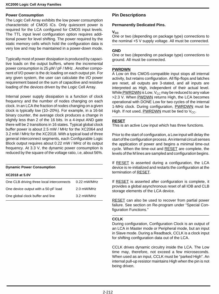
Power
Power DistributionPower for the LCA is distributed through a grid to achievehigh noise immunity and isolation between logic and I/O.For packages having more than 48 pins, two VCC pins andtwo ground pins are provided (see Figure 20). Inside theLCA device, a dedicated VCC and ground ring surroundingthe logic array provides power to the I/O drivers. An
1.00
0.80
0.60
0.40
0.20
SPECIFIED WORST-CASE VALUES
MAX COMMERCIAL (4.75 V)
MAX MILITARY (4.5 V)
– 55
MIN MILITARY (5.5 V)MIN COMMERCIAL (7.5 V)
MIN COMMERCIAL (5.25 V)
TYPICAL COMMERCIAL (+ 5.0 V, 25°C)
TYPICAL MILITARY
TEMPERATURE (°C)
– 40 – 20 0 25 40 70 80 100 125
NO
RM
ALI
ZE
D D
ELA
Y
MIN MILITARY (4.5 V)
Figure 19. Relative Delay as a Function of Temperature, Supply Voltage and Processing Variations
X1045
2-211
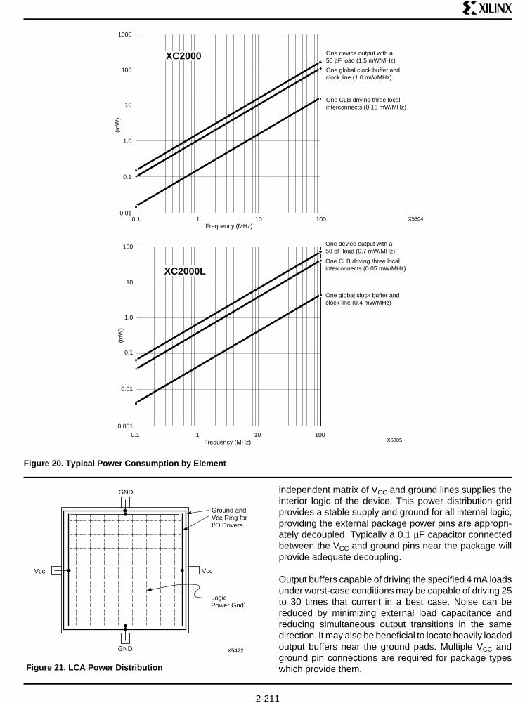
One CLB driving three local interconnects (0.05 mW/MHz)
One global clock buffer and clock line (0.4 mW/MHz)
One device output with a 50 pF load (0.7 mW/MHz)
0.001
0.01
0.1
1.0
10
100
0.1 1 10 100Frequency (MHz)
(m
W)
X5305
XC2000L
independent matrix of VCC and ground lines supplies theinterior logic of the device. This power distribution gridprovides a stable supply and ground for all internal logic,providing the external package power pins are appropri-ately decoupled. Typically a 0.1 µF capacitor connectedbetween the VCC and ground pins near the package willprovide adequate decoupling.
Output buffers capable of driving the specified 4 mA loadsunder worst-case conditions may be capable of driving 25to 30 times that current in a best case. Noise can bereduced by minimizing external load capacitance andreducing simultaneous output transitions in the samedirection. It may also be beneficial to locate heavily loadedoutput buffers near the ground pads. Multiple VCC andground pin connections are required for package typeswhich provide them.Figure 21. LCA Power Distribution
Figure 20. Typical Power Consumption by Element
One CLB driving three local interconnects (0.15 mW/MHz)
One global clock buffer and clock line (1.0 mW/MHz)
One device output with a 50 pF load (1.5 mW/MHz)
0.01
0.1
1.0
10
100
1000
0.1 1 10 100Frequency (MHz)
(m
W)
X5304
XC2000
GND
Ground and Vcc Ring for I/O Drivers
Vcc
GND
Vcc
Logic Power Grid
X5422
XC2000 Logic Cell Array Families
2-212
Pin Descriptions
Permanently Dedicated Pins.
VCCOne or two (depending on package type) connections tothe nominal +5 V supply voltage. All must be connected.
GNDOne or two (depending on package type) connections toground. All must be connected.
PWRDWNA Low on this CMOS-compatible input stops all internalactivity, but retains configuration. All flip-flops and latchesare reset, all outputs are 3-stated, and all inputs areinterpreted as High, independent of their actual level.While PWRDWN is Low, VCC may be reduced to any value>2.3 V. When PWDWN returns High, the LCA becomesoperational with DONE Low for two cycles of the internal1-MHz clock. During configuration, PWRDWN must beHigh. If not used, PWRDWN must be tied to VCC.
RESETThis is an active Low input which has three functions.
Prior to the start of configuration, a Low input will delay thestart of the configuration process. An internal circuit sensesthe application of power and begins a minimal time-outcycle. When the time-out and RESET are complete, thelevels of the M lines are sampled and configuration begins.
If RESET is asserted during a configuration, the LCAdevice is re-initialized and restarts the configuration at thetermination of RESET.
If RESET is asserted after configuration is complete, itprovides a global asynchronous reset of all IOB and CLBstorage elements of the LCA device.
RESET can also be used to recover from partial powerfailure. See section on Re-program under “Special Con-figuration Functions.”
CCLKDuring configuration, Configuration Clock is an output ofan LCA in Master mode or Peripheral mode, but an inputin Slave mode. During a Readback, CCLK is a clock inputfor shifting configuration data out of the LCA.
CCLK drives dynamic circuitry inside the LCA. The Lowtime may, therefore, not exceed a few microseconds.When used as an input, CCLK must be “parked High”. Aninternal pull-up resistor maintains High when the pin is notbeing driven.
Power ConsumptionThe Logic Cell Array exhibits the low power consumptioncharacteristic of CMOS ICs. Only quiescent power isrequired for the LCA configured for CMOS input levels.The TTL input level configuration option requires addi-tional power for level shifting. The power required by thestatic memory cells which hold the configuration data isvery low and may be maintained in a power-down mode.
Typically most of power dissipation is produced by capaci-tive loads on the output buffers, where the incrementalpower consumption is 25 µW / pF / MHz . Another compo-nent of I/O power is the dc loading on each output pin. Forany given system, the user can calculate the I/O powerrequirement based on the sum of capacitive and resistiveloading of the devices driven by the Logic Cell Array.
Internal power supply dissipation is a function of clockfrequency and the number of nodes changing on eachclock. In an LCA the fraction of nodes changing on a givenclock is typically low (10–20%). For example, in a 16-bitbinary counter, the average clock produces a change inslightly less than 2 of the 16 bits. In a 4-input AND gatethere will be 2 transitions in 16 states. Typical global clockbuffer power is about 2.5 mW / MHz for the XC2064 and3.2 mW / MHz for the XC2018. With a typical load of threegeneral interconnect segments, each Configurable LogicBlock output requires about 0.22 mW / MHz of its outputfrequency. At 3.3 V, the dynamic power consumption isreduced by the square of the voltage ratio, i.e, about 56%.
Dynamic Power Consumption
XC2018 at 5.0V
One CLB driving three local interconnects 0.22 mW/MHz
One device output with a 50-pF load 2.0 mW/MHz
One global clock buffer and line 3.2 mW/MHz

2-213
DONE/PROG (D/P)DONE is an open-drain output, configurable with or with-out an internal pull-up resistor. At the completion of con-figuration, the LCA circuitry becomes active in a synchro-nous order; DONE goes active High one cycle after theIOB outputs go active.
Once configuration is done, a High-to-Low transition ofthis pin will cause an initialization of the LCA and start areconfiguration.
M0/RTRIGAs Mode 0, this input and M1, M2 are sampled before thestart of configuration to establish the configuration mode tobe used.
A Low-to-High input transition, after configuration is com-plete, acts as a Read Trigger and initiates a Readback ofconfiguration and storage-element data clocked by CCLK.By selecting the appropriate Readback option when gen-erating the bitstream, this operation may be limited to asingle Readback, or be inhibited altogether.
M1/RDATAAs Mode 1, this input and M0, M2 are sampled before thestart of configuration to establish the configuration mode tobe used. If Readback is never used, M1 can be tied directlyto ground or VCC. If Readback is ever used, M1 must usea 5-kΩ resistor to ground or VCC, to accommodate theRDATA output.
As an active Low Read Data, after configuration is com-plete, this pin is the output of the Readback data.
User I/O Pins that can have special functions.
M2During configuration, this input has a weak pull-up resistor.Together with M0 and M1, it is sampled before the start ofconfiguration to establish the configuration mode to beused. After configuration, this pin is a user-programmableI/O pin.
HDCDuring configuration, this output is held at a High level toindicate that configuration is not yet complete. After con-figuration, this pin is a user-programmable I/O pin.
LDCDuring Configuration, this output is held at a Low level toindicate that the configuration is not yet complete. Afterconfiguration, this pin is a user-programmable I/O pin.LDC is particularly useful in Master mode as a Low enablefor an EPROM, but it must then be programmed as a Highafter configuration.
XTL1This user I/O pin can be used to operate as the output ofan amplifier driving an external crystal and bias circuitry.
XTL2This user I/O pin can be used as the input of an amplifierconnected to an external crystal and bias circuitry. The I/O Block is left unconfigured. The oscillator configuration isactivated by routing a net from the oscillator buffer symboloutput and by the MakeBits program.
CS0, CS1, CS2, WRTThese four inputs represent a set of signals, three activeLow and one active High, that are used to controlconfiguration-data entry in the Peripheral mode.Simultaneous assertion of all four inputs generates aWrite to the internal data buffer. The removal of anyassertion clocks in the D0-D7 data. In Master mode,thesepins become part of the parallel configuration byte, D4, D3,D2, D1. After configuration, these pins are user-programmable I/O pins.
RCLKDuring Master mode configuration RCLK represents a“read” of an external dynamic memory device (normallynot used). After configuration, this is a user-programmableI/O pin.
D0–D7This set of eight pins represents the parallel configurationinput for the parallel Master mode. After configuration iscomplete they are user programmed I/O pins.
A0–A15During Master Parallel mode, these 16 pins present anaddress output for a configuration EPROM. After configu-ration, they are user-programmable I/O pins.
DINDuring Slave or Master Serial configuration, this pin isused as a serial-data input. In the Master or Peripheralconfiguration, this is the Data 0 input. After configuration,this is a user-programmable I/O pin.
DOUTDuring configuration this pin is used to output serial-configuration data to the DIN pin of a daisy-chained slave.After configuration, this is a user-programmable I/O pin.
Unrestricted User I/O Pins.
I/OAn I/O pin may be programmed by the user to be an Inputor an Output pin following configuration. All unrestricted I/O pins, plus the special pins mentioned on the followingpage, have a weak pull-up resistor of 40 to 100 kΩ thatbecomes active as soon as the device powers up, andstays active until the end of configuration.

XC2000 Logic Cell Array Families
2-214
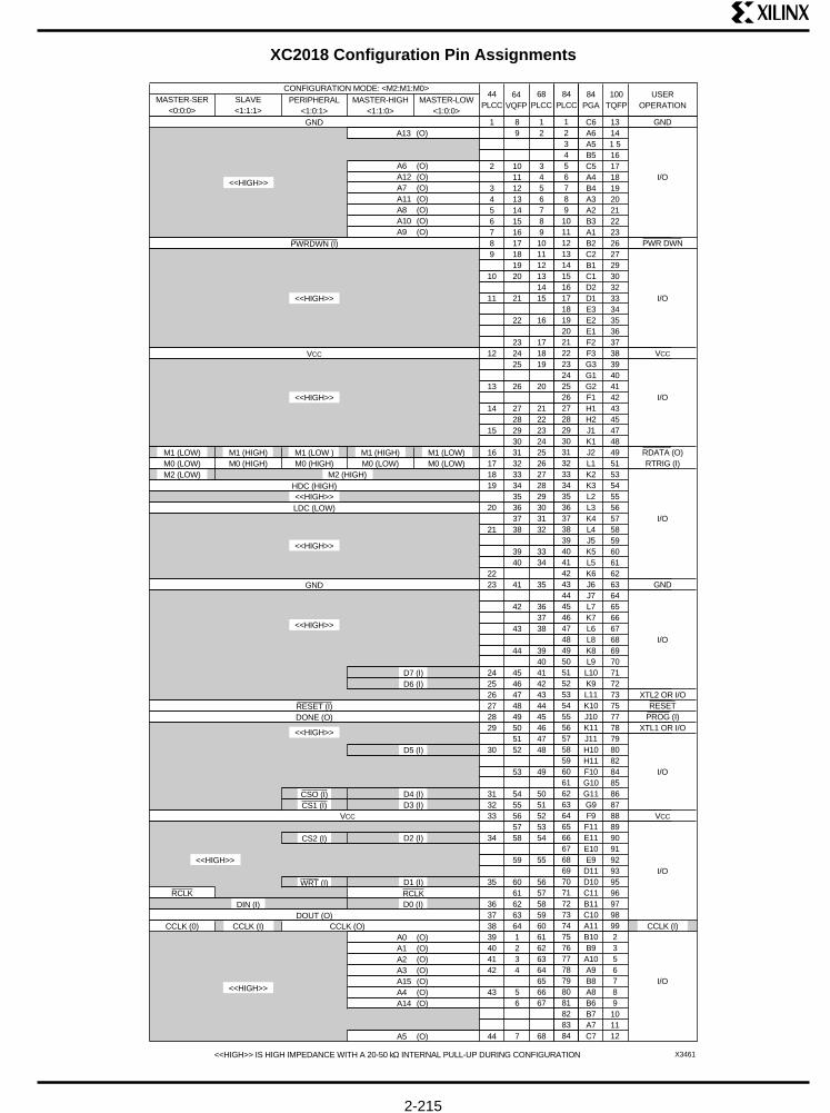
XC2064 Configuration Pin Assignments
Note: A PLCC in a “PGA-Footprint” socket has a different signal pinout than a PGA device.
1 2 3 4 5 6 7 8 9
10 11 12 13 14 15 16 17 18 19 20 21 22 23 24 25 26 27 28 29 30 31 32 33 34 35 36 37 38 39 40 41 42 43 44 45 46 47 48 49 50 51 52 53 54 55 56 57 58 59 60 61 62 63 64 65 66 67 68
1
2 3 4 5 6 7 8
9
10
11 12 13
14
15 16 17 18 19 20
21
22
23 24
25
26 27 28 29 30 31 32 33
34
35 36
37
38 39 40 41 42 43 44 45 46
47
48
1
2
3 4 5 6 7 8 9
10 11
12 13 14 15
16 17 18 19
20
21 22
23
24 25 26 27 28 29
30
31 32 33
34
35
36 37 38 39 40 41 42
43
44
B6 A6 B5 A5 B4 A4 B3 A3 A2 B2 B1 C2 C1 D2 D1 E2 E1 F2 F1 G2 G1 H2 H1 J2 J1 K1 K2 L2 K3 L3 K4 L4 K5 L5 K6 L6 K7 L7 K8 L8 K9 L9
L10 K10 K11 J10 J11 H10 H11 G10 G11 F10 F11 E10 E11 D10 D11 C10 C11 B11 B10 A10 B9 A9 D8 A8 B7 A7
GND
PWR DWN
VCC
RDATA (O)RTRIG (I)
GND
XTL2 OR I/ORESET
PROG (I)XTL1 OR I/O
VCC
CCLK (I)
User Operation
I/O
I/O
I/O
I/O
I/O
I/O
I/O
I/O
D7 (I) D6 (I)
D5 (I)
D4 (I) D3 (I)
D2 (I)
D1 (I) RCLK D0 (I)
A0
A1 A2 A3
A15 A4
A14 A5
(O) (O) (O) (O) (O) (O) (O) (O)
A13 A6
A12 A7
A11 A8
A10 A9
(O) (O) (O) (O) (O) (O) (O) (O)
GND
PWRDWN (I)
<<HIGH>>
VCC
M1 (LOW) M0 (HIGH) M2 (HIGH)
HDC (HIGH) <<HIGH>> LDC (LOW)
GND
<<HIGH>>
RESET (I) DONE (O)
CS0 (I) CS1 (I)
CS2 (I)
WRT (I)
Vcc
DOUT (O) CCLK (O) CCLK (I)
<<HIGH>>
DIN (I)
<<HIGH>>
<<HIGH>>
CCLK (O)
RCLK
M1 (LOW) M0 (LOW) M2 (LOW)
M1 (HIGH) M0 (HIGH)
M1 (HIGH) M0 (LOW)
M1 (LOW) M0 (LOW)
<<HIGH>>
<<HIGH>>
<<HIGH>>
PERIPHERAL <1:0:1>
Configuration Mode: <M2:M1:M0>
SLAVE <1:1:1>
MASTER-SET <0:0:0>
44 PLCC
48 DIP
68 PLCC
68 PGA
MASTER-HIGH <1:1:0>
<<HIGH>> is high impedance with a 20-50 kΩ internal pull-up during configuration X6103
MASTER-LOW <1:0:0>
2-215
1
2
3456789
10
11
12
13
14
15
16171819
20
21
2223
242526272829
30
313233
34
35
36373839404142
43
44
12
3456789101112131415
16
171819
20
212223242526272829303132
3334
35
363738
39404142434445464748
49
5051525354
55
565758596061626364656667
68
123456789101112131415161718192021222324252627282930313233343536373839404142434445464748495051525354555657585960616263646566676869707172737475767778798081828384
CONFIGURATION MODE: <M2:M1:M0>MASTER-SER
<0:0:0>SLAVE<1:1:1>
PERIPHERAL<1:0:1>
MASTER-HIGH<1:1:0>
MASTER-LOW<1:0:0>
44PLCC
68PLCC
84PLCC
A6 (O)A12 (O)A7 (O)A11 (O)A8 (O)A10 (O)A9 (O)
A13 (O)
PWRDWN (I)
VCC
M1 (LOW )M0 (HIGH)
<<HIGH>>LDC (LOW)
M2 (HIGH)
M1 (HIGH)M0 (LOW)
M1 (LOW)M0 (LOW)
M1 (HIGH)M0 (HIGH)M0 (LOW)
<<HIGH>>
GND
<<HIGH>>
D7 (I)D6 (I)
RESET (I)DONE (O)
<<HIGH>>
D5 (I)
CSO (I)CS1 (I)
D4 (I)D3 (I)
D2 (I)CS2 (I)
D1 (I)WRT (I)
D0 (I)RCLK
DIN (I)
<<HIGH>>
A0 (O)A1 (O)A2 (O)A3 (O)A15 (O)A4 (O)A14 (O)
A5 (O)
<<HIGH>>
GND
<<HIGH>>
<<HIGH>>
<<HIGH>>
HDC (HIGH)
VCC
CCLK (O)CCLK (I)DOUT (O)
CCLK (0)
<<HIGH>> IS HIGH IMPEDANCE WITH A 20-50 kΩ INTERNAL PULL-UP DURING CONFIGURATION X3461
RCLK
M1 (LOW)
M2 (LOW)
C6A6A5B5C5A4B4A3A2B3A1B2C2B1C1D2D1E3E2E1F2F3G3G1G2F1H1H2J1K1J2L1K2K3L2L3K4L4J5K5L5K6J6J7L7K7L6L8K8L9L10K9L11K10J10K11J11H10H11F10G10G11G9F9F11E11E10E9
D11D10C11B11C10A11B10B9A10A9B8A8B6B7A7C7
84PGA
USEROPERATION
13141 516171819202122232627293032333435363738394041424345474849515354555657585960616263646566676869707172737577787980828485868788899091929395969798992356789101112
100TQFP
GND
I/O
PWR DWN
I/O
VCC
I/O
RDATA (O)RTRIG (I)
I/O
GND
I/O
XTL2 OR I/ORESET
PROG (I)XTL1 OR I/O
I/O
VCC
I/O
CCLK (I)
I/O
89
1011121314151617181920
21
22
232425
26
272829303132333435363738
3940
41
42
43
44
4546474849505152
53
5455565758
59
60616263641234
56
7
64VQFP
XC2018 Configuration Pin Assignments
XC2000 Logic Cell Array Families
2-216
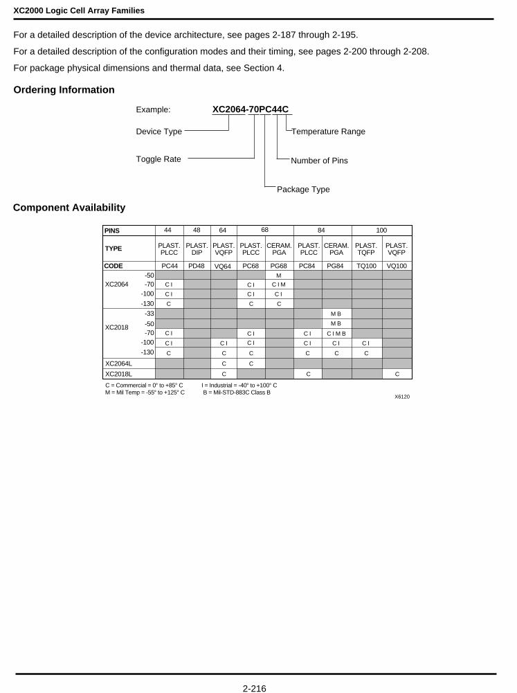
For a detailed description of the device architecture, see pages 2-187 through 2-195.
For a detailed description of the configuration modes and their timing, see pages 2-200 through 2-208.
For package physical dimensions and thermal data, see Section 4.
Ordering Information
Package Type
Device Type
Number of Pins
Temperature Range
Example: XC2064-70PC44C
Toggle Rate
Component Availability
PINS
TYPE
CODE
44 48 64 68 84 100
PLAST. PLCC
PLAST. DIP
PLAST. VQFP
PLAST. PLCC
CERAM. PGA
PLAST. PLCC
CERAM. PGA
PLAST. TQFP
PLAST. VQFP
PD48 VQ64 PC68 PG68PC44 PC84 PG84 TQ100 VQ100-50
-100
-130
-70
-50
-100
-130
-70
XC2064
XC2018
-33
XC2064L
XC2018L
C I
C I
C I
C I
C I
C I
C I
C IC I C I
C I
C I C I
C I
C
C C C CC
C
C C C
C I M
M
M B
M B
C I M B
C = Commercial = 0° to +85° CM = Mil Temp = -55° to +125° C
I = Industrial = -40° to +100° CB = Mil-STD-883C Class B
X6120
C
C C
C


![[Array, Array, Array, Array, Array, Array, Array, Array, Array, Array, Array, Array]](https://img.dokumen.tips/doc/110x75/56816460550346895dd63b8b/array-array-array-array-array-array-array-array-array-array-array.jpg)