Embed Size (px)
DESCRIPTION
driving ADC module of Xilinx
Citation preview

XAPP795 (v1.0) December 12, 2012 www.xilinx.com 1
© Copyright 2012 Xilinx, Inc. Xilinx, the Xilinx logo, Artix, ISE, Kintex, Spartan, Virtex, Vivado, Zynq, and other designated brands included herein are trademarks of Xilinx in the United States and other countries. All other trademarks are the property of their respective owners.
Summary Driving analog-to-digital converters (ADCs) is an extremely well documented subject, and there exists a vast amount of publicly available information on the topic. This application note provides the board designer with simple guidelines for common use cases of the Xilinx 7 series FPGAs analog-to-digital convertor (XADC). Following the guidelines outlined in this application note will ensure optimum performance when driving the XADC. Layout guidelines for the XADC are described in XADC Layout Guidelines [Ref 1]. For information about the Analog Mixed Signal (AMS) capabilities of 7 series devices, go to www.xilinx.com/ams.
XADC From the external printed circuit board (PCB), the XADC inputs can be viewed as a switched capacitor circuit similar to a traditional successive approximation register (SAR) ADC. Figure 1 illustrates an equivalent circuit for both unipolar and bipolar modes of the XADC.
Similar to other ADCs, the XADC relies on the accuracy of the voltage across the capacitor, CSAMPLE, for the accuracy of its conversion. A resistor and capacitor (RC) circuit as shown in Figure 1 takes a finite amount of time to settle to final voltage. The required accuracy of the signal is defined by the desired level of system accuracy. Given that the XADC is 12 bits, the minimum likely settling error would be less than one half of the least significant bit (LSB) of a 12-bit value (13 bits of accuracy).
Analysis of an RC Circuit
Before each use case of the XADC is analyzed, a simple RC circuit as shown in Figure 2 is analyzed. This analysis forms the basis for subsequent detailed analysis of each individual use case.
Application Note: 7 Series FPGAs
XAPP795 (v1.0) December 12, 2012
Driving the Xilinx Analog-to-Digital ConverterAuthor: Cathal Murphy
X-Ref Target - Figure 1
Figure 1: The XADC Input Equivalent Circuit During Acquisition
To ADC
Unipolar Mode
3 pF
RMUXVP
VN
Dedicated Inputs 100ΩAuxiliary Inputs 10 kΩ
Dedicated Inputs 100ΩAuxiliary Inputs 10 kΩ
X795_01_092612
RMUX
CSAMPLE
Bipolar Mode
VP
VN
Dedicated Inputs 100ΩAuxiliary Inputs 10 kΩ
Dedicated Inputs 100ΩAuxiliary Inputs 10 kΩ
To ADC3 pF
CSAMPLE
3 pF
RMUX
RMUX
CSAMPLE

XADC
XAPP795 (v1.0) December 12, 2012 www.xilinx.com 2
The response of the circuit shown in Figure 2 can be simulated when a step input is applied. This simulation allows the calculation of the settling time for an RC circuit. Figure 3 shows the output voltage (VOUT) of the RC circuit to a step voltage at its input (VIN) at t = 1 µs. The response of the circuit is exponential in nature. As time progresses, the desired output voltage is approached.
Assuming an initial voltage of zero across the capacitor, the circuit response is governed by Equation 1.
Equation 1
X-Ref Target - Figure 2
Figure 2: Simple RC Circuit with Ideal Source
X-Ref Target - Figure 3
Figure 3: Simulation Plot of the Step Response of an RC Circuit
X795_02_101112
RC Circuit
R1
C1
1 nF
50ΩV1
–
+
VIN VOUT
1.0
0.9
0.8
0.7
0.6
0.5
0.4
0.3
0.2
0.1
0.0
0.0 0.2 0.4 0.6 0.8 1.0 1.2 1.4 1.6 1.8 2.0
(µs)
(V)V(vout)V(vin)
X795_03_092712
VOUT t( ) vin 1 e
tRC---------–
–
=

XADC
XAPP795 (v1.0) December 12, 2012 www.xilinx.com 3
Equation 1 indicates that as time increases, the error associated with the settling of the circuit decreases proportionally to the RC product known as the time constant, τ. The smaller the time constant, the faster the error term approaches an acceptable level.
Designers typically have an error budget measured in the number of bits or error percentage that must be achieved. Normally, the settling error would not be equal to the full error budget. Instead, one half of the total budget would be allowed for settling error. For an error budget of 12 bits or 0.025%, enough settling time for 13 bits or 0.0125% would be allowed. Table 1 shows the time constant values required for a one half LSB error for each of the ADC resolutions.
Equation 2 shows how to calculate the settling time for an RC circuit for various levels of accuracy.
Equation 2
The first step to using Equation 2 is to find the required number of time constants in Table 1 to achieve the appropriate level of accuracy. For example, 12 bits of accuracy requires 9.01 time constants.
In the RC filter that makes up the equivalent circuit for the XADC input during the tracking phase in unipolar mode, the settling time required is given by Equation 3.
Equation 3
Given that the total acquisition time of the XADC is 750 ns, there is no issue with settling the XADC input circuit in this instance. Settling time issues can arise due to the source impedance of the driving circuit (resistor divider application) or due to other poles in the system (other RC circuits or in the active source itself) at lower frequencies. These issues are discussed individually in subsequent sections of this application note.
Issues Associated with Inadequate Settling Time
Failure to provide sufficient settling time means that the sampling capacitor cannot settle to its final accurate voltage resulting in a number of unwanted effects:
• ADC gain errors
• Temperature sensitivity to ADC gain error
• Crosstalk when using an external multiplexer
These issues occur with a majority of ADCs that use this type of switched capacitor input scheme. However, with some understanding and care, it is easy to avoid these issues when designing the analog input circuit for the XADC. Numerous tutorials and reference materials are available, such as Designing SAR ADC Drive Circuitry, Part II [Ref 2], Designing SAR ADC Drive Circuitry, Part III [Ref 3], Analog-to-Digital Confusion: Pitfalls of Driving an ADC [Ref 4], and Switched-Capacitor ADC Analog Input Calculations [Ref 5]. This application note addresses the specific requirements of the 7 series FPGAs XADC.
Table 1: Time Constant Values Required for Specific Resolutions
Resolution (bits) Error (%) Number of Time Constants
6 0.3906 4.85
8 0.0977 6.24
10 0.0244 7.62
12 0.0061 9.01
14 0.0015 10.4
tsettle Number of Time Constants( ) RC×=
tsettle 9.01 2 10kΩ 3pF××× 540ns= =

XADC
XAPP795 (v1.0) December 12, 2012 www.xilinx.com 4
Unique Benefits of XADC
The sampling period of an ADC is typically made up of two time periods: conversion time and acquisition time. During the acquisition time period, the ADC starts to acquire its next sample which is digitized in the conversion phase. In many ADCs, the acquisition time period can be as little as 10% of the overall conversion time. In some 1 MSPS ADCs, only 100 ns are available for the ADC to acquire its next sample. Consequently, whatever is driving the ADC needs to be capable of driving the capacitive load presented by the ADC and to settle within 100 ns. This requirement can be a significant challenge to meet.
The XADC addresses this issue by allowing the conversion and acquisition phases to occur in parallel resulting in greater than 75% of the overall sample time being available for acquisition, as shown in Figure 4. This arrangement significantly reduces the requirements for the analog front end driving the XADC, the benefit of which is illustrated in each of the use cases analyzed in subsequent sections of this application note.
Anti-Aliasing Filter Requirements
As with all ADCs, it is recommended that an anti-aliasing filter (AAF) be used and that it be placed as close to the inputs to the XADC as possible. This AAF stops unwanted high-frequency components of the signal from aliasing back into the bandwidth of interest due to the nature of the sampling process and impacting the performance of the XADC (see What the Nyquist Criterion Means to Your Sampled Data System Design [Ref 6]).
Ideally, the maximum cut-off frequency of the AAF should be the Nyquist rate of the converter. For an XADC running at 1 MSPS, the Nyquist frequency is 500 KHz when a single channel is being converted. The Nyquist frequency reduces linearly with the number of channels that are multiplexed into the 1 MSPS ADC. In general, it is not possible to have an AAF with a cut-off at the Nyquist frequency due to its impact on the settling time of the circuit. This issue is covered in subsequent sections of this application note.
X-Ref Target - Figure 4
Figure 4: Acquisition and Conversion Timing Diagram
X795_04_092612
ACLK
BUSY
Acquisition and ConversionRunning in Parallel
15 1 5 6 26 1 26 1
EOC/EOS
tadk
tsample
tconversion
tacquisition
XADC Use Case Examples
XAPP795 (v1.0) December 12, 2012 www.xilinx.com 5
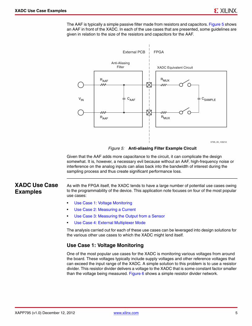
The AAF is typically a simple passive filter made from resistors and capacitors. Figure 5 shows an AAF in front of the XADC. In each of the use cases that are presented, some guidelines are given in relation to the size of the resistors and capacitors for the AAF.
Given that the AAF adds more capacitance to the circuit, it can complicate the design somewhat. It is, however, a necessary evil because without an AAF, high-frequency noise or interference on the analog inputs can alias back into the bandwidth of interest during the sampling process and thus create significant performance loss.
XADC Use Case Examples
As with the FPGA itself, the XADC tends to have a large number of potential use cases owing to the programmability of the device. This application note focuses on four of the most popular use cases:
• Use Case 1: Voltage Monitoring
• Use Case 2: Measuring a Current
• Use Case 3: Measuring the Output from a Sensor
• Use Case 4: External Multiplexer Mode
The analysis carried out for each of these use cases can be leveraged into design solutions for the various other use cases to which the XADC might lend itself.
Use Case 1: Voltage Monitoring
One of the most popular use cases for the XADC is monitoring various voltages from around the board. These voltages typically include supply voltages and other reference voltages that can exceed the input range of the XADC. A simple solution to this problem is to use a resistor divider. This resistor divider delivers a voltage to the XADC that is some constant factor smaller than the voltage being measured. Figure 6 shows a simple resistor divider network.
X-Ref Target - Figure 5
Figure 5: Anti-aliasing Filter Example Circuit
X795_05_100212
External PCB
Anti-AliasingFilter
FPGA
XADC Equivalent Circuit
CSAMPLE
RMUX
VIN
RAAF
RAAF
CAAF
RMUX

XADC Use Case Examples
XAPP795 (v1.0) December 12, 2012 www.xilinx.com 6
Equation 4 defines the VXADC for the circuit shown in Figure 6.
Equation 4
Consider the case where VMON is 5V and the desired VXADC is 0.5V. This places VXADC in the middle of the XADC range and thus allows sampling VMON voltages of up to 10V and down to 0V, as shown in Equation 5.
Equation 5
Or R1 = 9R2. Thus, if R2 = 1 kΩ, R1 = 9 kΩ .
Ideally, the resistor values should be kept as low as possible to ensure that leakage current effects have minimal impact. The power consumption of the resistor divider network ultimately decides how low a resistance is tolerable.
The impact of this resistor divider on the settling time of the overall circuit including the AAF is shown in Figure 7. The settling time of the XADC equivalent circuit can be ignored because it is quick enough by itself (see Equation 3, page 3), and the AAF capacitor is many times larger than the CSAMPLE value.
R1|R2 is the parallel combination of R1 and R2 where R1 is 1 kΩ and R2 is 9 kΩ. This equates to 900Ω, which is typically much larger than RAAF, and thus RAAF can be ignored.
For monitoring various voltages around the board, typically sampling them at a 10 µs (100 Ks/s) sample rate is sufficient. To ensure a settling time of one half of a 12 bit LSB, CAAF must be sized using Equation 6.
Equation 6
X-Ref Target - Figure 6
Figure 6: Resistor Divider Circuit
X-Ref Target - Figure 7
Figure 7: Resistor Divider Circuit
X795_06_100212
VMON
VXADC
R1
R2
VXADC VMONR2
R1 R2+----------------------=
VXADC
VMON------------------
0.55
-------- 0.10 R2R1 R2+----------------------= = =
X795_07_100212
VSRC CAAF
RAAFR1/R2
tsettle 10μs 9.01 R1 R2× CAAF×= =

XADC Use Case Examples
XAPP795 (v1.0) December 12, 2012 www.xilinx.com 7
This implies that CAAF can be sized as shown in Equation 7.
Equation 7
The cutoff frequency for this RC circuit is 160 kHz, which is considerably larger than the Nyquist frequency (50 KHz) for an ADC running at 100 Ks/s. This is because a filter with a cutoff frequency of 50 KHz does not settle to 12 bits of accuracy in 10 µs.
In many cases, the accuracy requirement is less than 10 bits. Thus, the settling time requirements can be reduced by replacing the 9.01 in Equation 7 with the appropriate number from Table 1, page 3.
Figure 8 shows a schematic with a resistor divider network being interfaced to the XADC input equivalent circuit with the passive components sized as calculated with Equation 6 and Equation 7.
Notes related to Figure 8:
1. Switches S1 and S2 should be closed during the period of the conversion labeled tacquistion in Figure 4, page 4.
2. During the ADC conversion process, the CSAMPLE capacitor gets reset. In any settling time simulation, CSAMPLE should be reset before the acquisition time begins.
CAAF10μs
9.01 R1 R2×------------------------------------
10μs9.01 900×---------------------------- 1.1nF∼= =
X-Ref Target - Figure 8
Figure 8: Resistor Divider Interfaced to XADC Simulation Circuit
Anti-Aliasing FilterVIN XADC Equivalent Circuit
CSAMPLE
C3S3
SW1
VXADCP
VXADCN
3 pFreset
acq
RMUX
SW1
SW1S2
S1
10 k
RAAF
VCAFFP
VCAFFN
AC 10
V2
250.01
R4
25
R5
R2
1k CAAF
R1
9k
C1
1.1 nF
acq
X795_08_100212
–+
– +
–+
–+
R3
R8
R9
RMUXRAAF

XADC Use Case Examples
XAPP795 (v1.0) December 12, 2012 www.xilinx.com 8
Figure 9 shows a simulation result showing that the circuit in Figure 8 settles to within 12 bits of accuracy in 9.725 μs. The settling time requirement reduces to 8 μs if only 10 bits of accuracy is needed.
A resistor divider circuit is shown in the Voltage Attenuation figure in 7 Series FPGAs XADC Dual 12-Bit 1MSPS Analog-to-Digital Converter User Guide [Ref 7]. In this circuit, a 4 kΩ resistor is placed in series with the resistor in the AAF on the N input side. The resistor is sized to equal the parallel combination of the two resistors that make up the resistor divider network. This resistor ensures that the impedance is balanced on both the P and N inputs to the XADC, helping to maximize the interference immunity of the circuit. This approach should be adopted when building a resistor divider circuit to drive the XADC. With this approach, the impact to the settling time of the circuit essentially doubles the size of the resistor in the RC circuit. Thus, to obtain the same settling times, the CAAF capacitor value must be reduced by a factor of 2 to 0.55 nF.
Use Case 2: Measuring a Current
Many ADC applications require measuring a current. The objective might be to measure the supply current or even the phase current of a motor. Typically, to measure a current flowing in a net, a resistor is placed directly in the current path, and the voltage drop across the resistor is measured. To ensure that there is not a significant voltage drop across the resistor, a value is selected that is a fraction of the total resistance of the load. A difference amplifier or instrumentation amplifier (in-amp) can be used to increase the gain of the voltage drop across the resistor to a level adequate for conversion by the ADC. These amplifier types can either be built up using discrete components or can come as a fully integrated solution. The most versatile and forgiving option is to use a fully integrated instrumentation amplifier, although this incurs an added cost. Tutorials are available that assist in choosing the best amplifier solution for a given situation (see Difference and Current Sense Amplifiers [Ref 8] and Instrumentation Amplifier (In-Amp) Basics [Ref 9]). Figure 10 shows a block diagram for such a current measurement circuit using an integrated differencing amplifier with built-in gain.
X-Ref Target - Figure 9
Figure 9: Simulation of Use Case 1 Showing Settling Time
1.0
10
9
8
7
6
5
4
3
2
1
0
0 1 2 3 4 5 6 7 8 9 10 11 12 13 14 15
(µs)
(V)
10.7248 µs, -0.5 lsbs
Step InputSettled to 1/2 of a
12-bit LSB
9.725 µs
((V(vxadcp)-V(vxadcn))-1V)/(1V/4096)
X795_09_111912
Err
or in
12-
bit L
SB
s 0.80.6
0.4
0.2
0.0-0.2
-0.4
-0.6-0.8
-1.0

XADC Use Case Examples
XAPP795 (v1.0) December 12, 2012 www.xilinx.com 9
Ideally, the solution shown in Figure 10 can be interfaced directly to an ADC. Certain ADCs might require a buffer or driving amplifier to be placed into the signal chain before the ADC. The XADC in general does not require a buffer amplifier. However, in certain applications the amplifier might be necessary to achieve the highest level of performance.
Driving the XADC with a Standard In-Amp
Typically, standard in-amps are slow with an input bandwidth in the 10 to 100 KHz range. This can affect the ability of the amplifier to capture fast changes in current but, in most cases, this is not an issue. The in-amp must also be fast enough to recharge the input sample capacitance presented during the ADC acquisition phase.
Because of the mismatch between the XADC sample rate of 1 MSPS and the bandwidth of the amplifier, the XADC should be slowed to give the amplifier adequate time to settle the sample capacitor. In most applications, however, slowing the XADC is not necessary given that the in-amp has a very narrow input bandwidth. For higher performance applications, running the XADC at 1 MSPS is required to allow the XADC result to be over sampled and decimated to meet the dynamic range requirements of the design. This topic is covered later in this section of the application note.
Before fully analyzing the circuit, another consideration is the need for some anti-aliasing filtering between the instrumentation or differencing amplifier and the XADC. Figure 11 shows an example circuit that includes the AAF. Typically, it is not necessary for this AAF to operate at the Nyquist frequency of the ADC as the majority of the noise exists at or above 1 MHz. Operating an anti-aliasing filter at the Nyquist frequency of the ADC taxes the system by reducing the response time of the in-amp. For this example, an AAF with a cutoff frequency of 500 KHz is used. This frequency does not adversely affect the settling time of the in-amp but does filter out unwanted signals appearing at the analog inputs such as high-frequency noise from the amplifier power supply.
X-Ref Target - Figure 10
Figure 10: Current Measuring Circuit Using Integrated Difference Amplifier
X795_10_100212
Differencing Amplifier
Gain = R1/R3
R1
R2
R3
VDIFF = RSHUNT x ILOAD
R4
in
in VOUTVOUT = (Gain x RSHUNT x ILOAD) + VCM
ILOAD
VSUPPLY
VREF
VCM
VCM
RSHUNT
Load
–
+

XADC Use Case Examples
XAPP795 (v1.0) December 12, 2012 www.xilinx.com 10
Equation 8 is used to implement an AAF with a cut-off frequency of 500 KHz.
Equation 8
The capacitance should be chosen by referencing the maximum load capacitance on the in-amp datasheet. The Texas Instruments INA210–INA214 Data Sheet [Ref 10] specifies a maximum capacitance of 1 nF. Using this specification, a value for RAAF can be calculated with Equation 9.
Equation 9
RAAF ≅ 150Ω
The next step is to determine the XADC sample rate at which the circuit settles to the required level of accuracy. This is determined by the maximum settling speed for the in-amp in question. Typically, the in-amp vendor quotes an input bandwidth specification that can be used to calculate the settling time of the circuit. However, this settling time often does not include a transient load effect response such as that caused by a switched capacitor circuit. The input response and the load response are of the same order with the load transient settling time being quicker. In this case, it is best to use the input bandwidth specification itself to calculate the settling time.
Another method is to just measure the response time, but this can be time consuming. Yet another approach is to use the SPICE models provided by the vendor, bearing in mind that these models might not deal with a load transient effect correctly resulting in a grossly underestimated settling time.
Equation 10 determines the sample rate of the XADC for a given amplifier bandwidth.
Equation 10
500KHz 12π 2RAAF( )CAAF---------------------------------------------=
6283k 1RAAFCAAF-----------------------------
1RAAF1nF--------------------------= =
X-Ref Target - Figure 11
Figure 11: Direct Digitization of Difference Amplifier Output by the XADC
X795_11_100312
Load
Load
FPGA
XADC Equivalent Circuit
External PCB
Anti-AliasingFilter
CAAF
Differencing Amplifier
Gain = R1/R3
R1
R2
R3
R4
in
in
–
––+
+ +
RAAF RMUX
RMUX
CSAMPLE
VSUPPLY
ILOAD
RSHUNTVDIFF = RSHUNT x
ILOAD
VOUT
VREF
VCM
RAAF
XADCSampleRate2π inampbw( )
τ------------------------------------=

XADC Use Case Examples
XAPP795 (v1.0) December 12, 2012 www.xilinx.com 11
For 12 bits of accuracy using the INA213 differencing amplifier (Texas Instruments INA210–INA214 Data Sheet [Ref 10] Figure 7), the XADC sample rate is given by Equation 11.
Equation 11
For applications requiring only 10 bits of accuracy, the XADC sample rate is given by Equation 12.
Equation 12
For higher performance applications, the XADC should be operated at 1 MSPS to allow the result to be oversampled and decimated to meet the dynamic range requirements of the design. In this instance, a buffer might be required. The cost trade-off must be evaluated between purchasing a high-performance in-amp and purchasing a lower performance in-amp with an additional buffer. The in-amp only drives the buffer amplifier and the buffer takes care of driving the switched capacitor load presented by the XADC, as shown in Figure 12.
Use Case 3: Measuring the Output from a Sensor
Another very common use case for the XADC is measuring the output from a sensor. Typical applications include a strain gauge or temperature sensor such as a resistance temperature detector (RTD). For both a strain gauge and an RTD, the sensor resistance changes with the parameter measured. A typical method of measuring this change in resistance is to build a Wheatstone bridge circuit, as shown in figure Figure 13, where three of the resistors in the bridge have fixed values and the variable-resistance sensor forms the fourth resistor. The voltage between the two mid-points of the bridge varies proportionally to the change in resistance of the sensor, thus becoming a measure of the parameter in question.
XADCSampleRate 2π 100kHz( )9.01
--------------------------------- 70KSPS≅=
XADCSampleRate 2π 100kHz( )7.62
--------------------------------- 80KSPS≅=
X-Ref Target - Figure 12
Figure 12: Current Measurement Using a Buffer to Drive the XADC
X795_12_100312
Load
Load
FPGA
XADC Equivalent Circuit
External PCB
Anti-AliasingFilter
Differencing Amplifier
Gain = R1/R3
R1
R2
R3
R4
in
in
–
––+
+ +
Buffer
VSUPPLY
ILOAD
RSHUNT VDIFF = RSHUNT x ILOAD
VOUT
VREF
VCM
RAAF
RAAF
CAAF
RMUX
RMUX
CSAMPLE

XADC Use Case Examples
XAPP795 (v1.0) December 12, 2012 www.xilinx.com 12
The Wheatstone bridge feeds an ADC to digitize the voltage VOUT. The bridge can interface directly to an instrumentation amplifier. A differencing amplifier is not used due to the loading effect caused by the series resistance it presents to the bridge. With this configuration, the circuit and analysis is the same as that in use case 2.
Sensor measurement requires a high degree of accuracy. Thus, the XADC should run as fast as possible to oversample or decimate its output to maximize the dynamic range. If the in-amp used does not have enough bandwidth to drive the XADC at these speeds, a buffer amplifier is required, similar to that shown in Figure 12.
Use Case 4: External Multiplexer Mode
Given the many uses for the XADC, it is common to have a shortage of spare I/O ports to connect all of the required external analog signals to the XADC. An easy solution to this problem is adding an external multiplexer (MUX) to the design. The external MUX reduces the number of required pins on the FPGA while allowing a large number of analog signals to be connected and digitized by the XADC. A block diagram of this solution is shown in Figure 14. The XADC also has some built-in features that allow this use case without additional FPGA coding. See the External Multiplexer Mode section of 7 Series FPGAs XADC Dual 12-Bit 1MSPS Analog-to-Digital Converter User Guide [Ref 7] for more details on these features.
X-Ref Target - Figure 13
Figure 13: Wheatstone Bridge Circuit for Measuring Change in Sensor Resistance
R1
R2
R3
VREF
VOUT
RVAR
X795_13_092712

XADC Use Case Examples
XAPP795 (v1.0) December 12, 2012 www.xilinx.com 13
Designing circuits that settle in time is a little more challenging and potentially less forgiving when using an external MUX. In prior cases, only the sample capacitor of the XADC needed to be recharged on every XADC sample. In the case of the external multiplexer, any external capacitance on the output side of the multiplexer must be completely charged to the desired voltage. This includes any board capacitance between the output of the MUX and the sample capacitor of the ADC, as well as any capacitance that makes up an AAF between the MUX output and the XADC input. The board capacitance alone is on the order of 10 pF and the AAF capacitor is much larger. In addition to the capacitance issue, settling errors in a multiplexed application can result in crosstalk from the previous channel selected by the multiplexer to the current channel. See Understanding Crosstalk in Analog Multiplexers [Ref 11].
Given the large number of analog input channels that are needed in such applications, slowing the XADC presents a problem as the bandwidth per channel quickly becomes too small. The XADC is run at the full 1 MSPS rate to provide each channel enough bandwidth. This means each channel that is connected to the multiplexer must be capable of driving the capacitance at the output of the multiplexer in less than 1 µs. This capability generally requires an operational amplifier.
Adding an operational amplifier to each pin can be expensive. An alternate solution is to place a single buffer directly at the output of the MUX. The buffer should be positioned as close as possible to the output side of the MUX to minimize the buffer input capacitance. Each channel must only drive the input of the amplifier within 1 µs. An anti-aliasing filter can be placed at the buffer output prior to the XADC to remove extraneous high-frequency signals. This AAF should be designed to settle within the allowed acquisition time of the XADC. Figure 15 shows a block diagram of a buffered external multiplexer.
X-Ref Target - Figure 14
Figure 14: External Multiplexer Mode
TemperatureSensor
°C
SupplySensors
MUX12 Bits
1 MSPSADC A
MUXADDR[4:0]
VP
VN
MUX
FPGAExternal Analog Multiplexer
16:1
ADDR
4
–
–+
+
–
–+
+
X795_14_092612

XADC Use Case Examples
XAPP795 (v1.0) December 12, 2012 www.xilinx.com 14
Given that the maximum linear settling time of the XADC input circuitry is 540 ns, the resistors and capacitors making up the AAF should be sized for a time constant of 9.01, which equates to approximately 500 ns. A settling time requirement of 500 ns ensures that the XADC and AAF settle within 75% (750 ns) of the sampling period (1 µs). This requires the AAF and the XADC sampling network to both settle in 750 ns. Thus, Equation 13 to Equation 15 must be true.
Equation 13
Equation 14
Equation 15
Assuming the AAF circuit shown in Figure 5, page 5, the AAF resistors and capacitors should be sized according to Equation 16.
Equation 16
Assuming CAAF is 1 nF, RAAF is approximately 25Ω.
Each input to the MUX must now be capable of driving the parasitic capacitance and the output of the MUX but not the AAF, the parasitic board capacitance, or the XADC input. If the board is carefully laid out, the capacitance can be limited to less than 5 pF, including the input capacitance of the buffer.
Resistor Divider External MUX Input
For a resistor divider circuit as shown in Figure 6, page 6, the maximum parallel combination of R1 and R2 is given in Equation 17.
Equation 17
X-Ref Target - Figure 15
Figure 15: External Multiplexer Use Case with Buffer at Multiplexer Output
X795_15_100312
Reduce CPAR
Raaf
RAAF
CAAF
TemperatureSensor
°C
SupplySensors
MUX12 Bits
1 MSPSADC A
MUXADDR[4:0]
VP
VN
MUX
FPGA
External Analog Multiplexer16:1
ADDR
4
–
–+
+
–
–+
+
Buffer
tsettleoveralltsettleAAF
( )2tsettleXADCinput
( )2+=
tsettleAAF( )2
750ns( )2540ns( )2
–=
tsettleAAF500ns∼
2RAAFCAAF500ns9.01
----------------- 55ns= =
R1 R2tsettle
τCPAR------------------
500ns9.01 5p( )----------------------- 55kΩ= = =

Conclusion
XAPP795 (v1.0) December 12, 2012 www.xilinx.com 15
The parallel combination of R1|R2 is typically less than 1 kΩ because of leakage concerns. Thus, keeping the resistance below 55 kΩ is not an issue, and there are no settling time concerns for the circuit.
In-amp External MUX Input
Some instrumentation amplifiers are too slow to drive the 5 pF of parasitic capacitance at the output of the external MUX. When using an external MUX, there are likely to be a large number of channels. Slowing the XADC to accommodate one slow channel driven by an in-amp requires all other channels to slow down as well when operating in automatic sequencer mode.
Because of this, it is recommended to follow each in-amp with a buffer prior to it being interfaced to the MUX. This buffer can easily drive the parasitic capacitance at the output of the MUX in much less than 500 ns.
Conclusion This application note illustrates the care that must be taken when driving ADCs with switched capacitor inputs. The XADC has a switched capacitor input but it also has some unique benefits that extend the acquisition time of the XADC when compared to other discrete ADCs.
This application note presents example solutions to driving the XADC in a number of common use cases. By following the simple guidelines presented, most analog interface requirements are easily accommodated.
References 1. XAPP554, XADC Layout Guidelines.
2. Downs, Rick, and Miro Oljaca. Designing SAR ADC Drive Circuitry, Part II. Texas Instruments, Inc.http://www.analogzone.com/acqt1003.pdf
3. Downs, Rick, and Miro Oljaca. Designing SAR ADC Drive Circuitry, Part III. Texas Instruments, Inc.http://www.analogzone.com/acqt0312.pdf
4. Sachs, Jason. 2011. Analog-to-Digital Confusion: Pitfalls of Driving an ADC.http://www.embeddedrelated.com/showarticle/110.php
5. Switched-Capacitor ADC Analog Input Calculations. Texas Instruments, Inc.http://www.ti.com/lit/an/slaa036/slaa036.pdf
6. What the Nyquist Criterion Means to Your Sampled Data System Design. Analog Devices.http://www.analog.com/static/imported-files/tutorials/MT-002.pdf
7. UG480, 7 Series FPGAs XADC Dual 12-Bit 1MSPS Analog-to-Digital Converter User Guide.
8. Difference and Current Sense Amplifiers. Analog Devices.http://www.analog.com/static/imported-files/tutorials/MT-068.pdf
9. Instrumentation Amplifier (In-Amp) Basics. Analog Devices.http://www.analog.com/static/imported-files/tutorials/MT-061.pdf
10. INA210–Data Sheet. Texas Instruments, Inc.http://www.ti.com/lit/ds/symlink/ina213.pdf
11. Understanding Crosstalk in Analog Multiplexers. Analog Devices.http://www.analog.com/static/imported-files/application_notes/177696709AN35.pdf
Revision History
XAPP795 (v1.0) December 12, 2012 www.xilinx.com 16
Revision History
The following table shows the revision history for this document.
Notice of Disclaimer
The information disclosed to you hereunder (the “Materials”) is provided solely for the selection and use ofXilinx products. To the maximum extent permitted by applicable law: (1) Materials are made available "ASIS" and with all faults, Xilinx hereby DISCLAIMS ALL WARRANTIES AND CONDITIONS, EXPRESS,IMPLIED, OR STATUTORY, INCLUDING BUT NOT LIMITED TO WARRANTIES OFMERCHANTABILITY, NON-INFRINGEMENT, OR FITNESS FOR ANY PARTICULAR PURPOSE; and (2)Xilinx shall not be liable (whether in contract or tort, including negligence, or under any other theory ofliability) for any loss or damage of any kind or nature related to, arising under, or in connection with, theMaterials (including your use of the Materials), including for any direct, indirect, special, incidental, orconsequential loss or damage (including loss of data, profits, goodwill, or any type of loss or damagesuffered as a result of any action brought by a third party) even if such damage or loss was reasonablyforeseeable or Xilinx had been advised of the possibility of the same. Xilinx assumes no obligation tocorrect any errors contained in the Materials or to notify you of updates to the Materials or to productspecifications. You may not reproduce, modify, distribute, or publicly display the Materials without priorwritten consent. Certain products are subject to the terms and conditions of the Limited Warranties whichcan be viewed at http://www.xilinx.com/warranty.htm; IP cores may be subject to warranty and supportterms contained in a license issued to you by Xilinx. Xilinx products are not designed or intended to befail-safe or for use in any application requiring fail-safe performance; you assume sole risk and liability foruse of Xilinx products in Critical Applications: http://www.xilinx.com/warranty.htm#critapps.
Date Version Description of Revisions
12/12/12 1.0 Initial Xilinx release.