Embed Size (px)
Citation preview
6th March 2013 1
X-ray photoelectron spectroscopy - An introduction
Spyros Diplas MENA3100
SINTEF Materials & Chemistry, Department of Materials Physics &
Centre of Materials Science and Nanotechnology, Department of Chemistry, UiO
6th March 2013 2
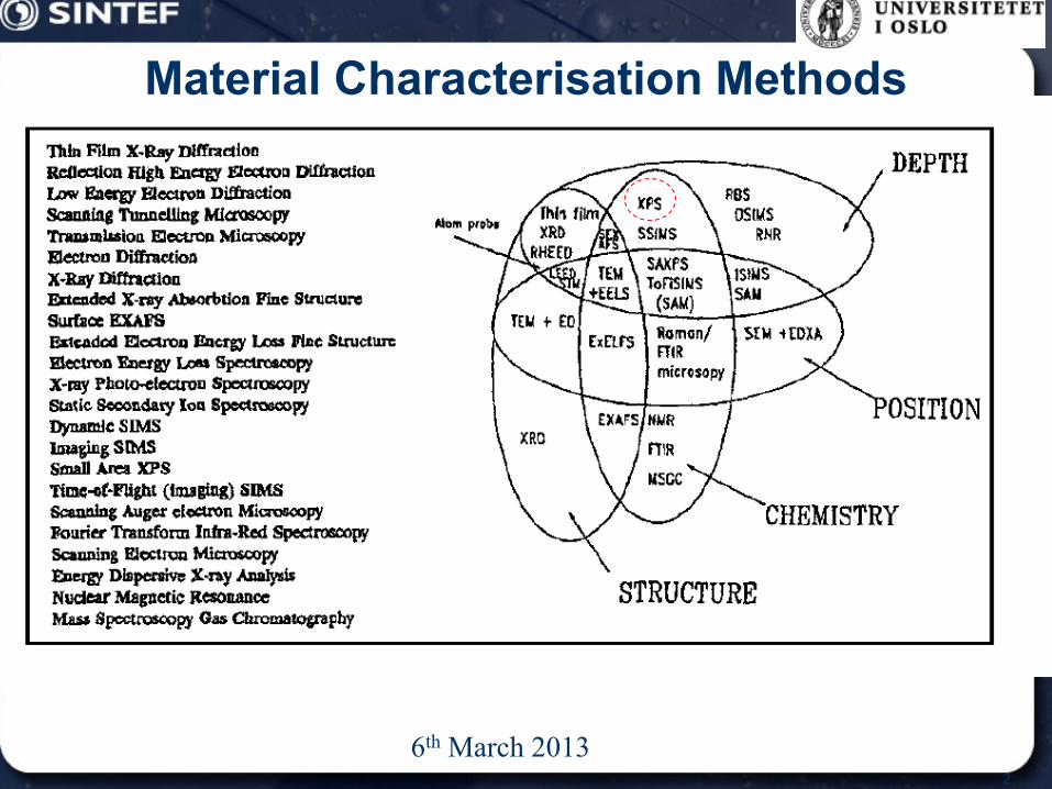
Material Characterisation Methods
6th March 2013 3
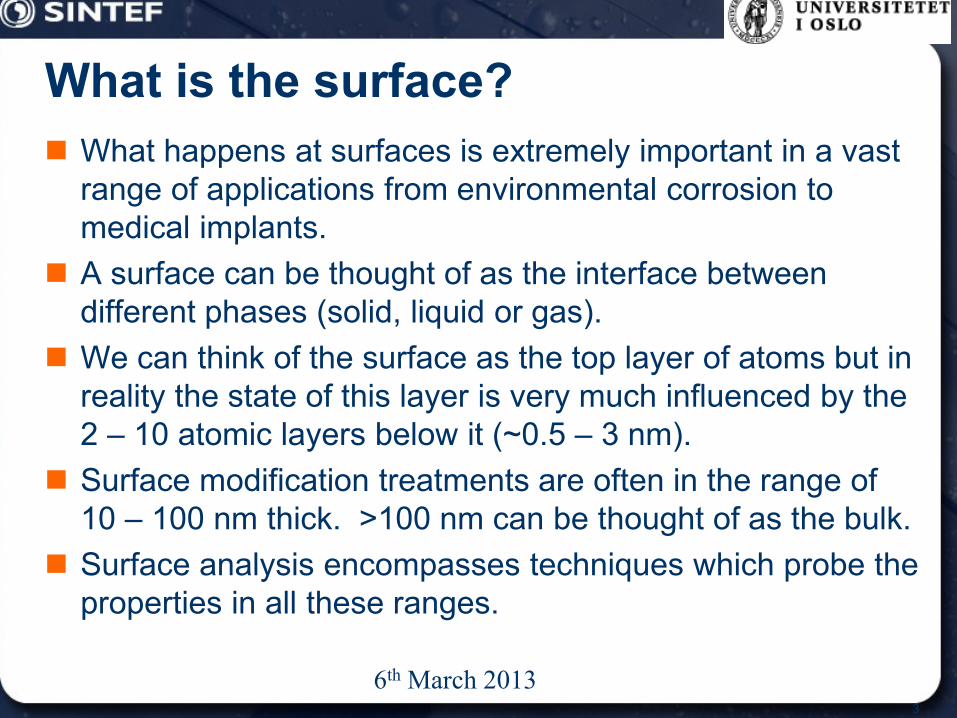
What is the surface? What happens at surfaces is extremely important in a vast
range of applications from environmental corrosion to medical implants.
A surface can be thought of as the interface between different phases (solid, liquid or gas).
We can think of the surface as the top layer of atoms but in reality the state of this layer is very much influenced by the 2 – 10 atomic layers below it (~0.5 – 3 nm).
Surface modification treatments are often in the range of 10 – 100 nm thick. >100 nm can be thought of as the bulk.
Surface analysis encompasses techniques which probe the properties in all these ranges.
6th March 2013 4
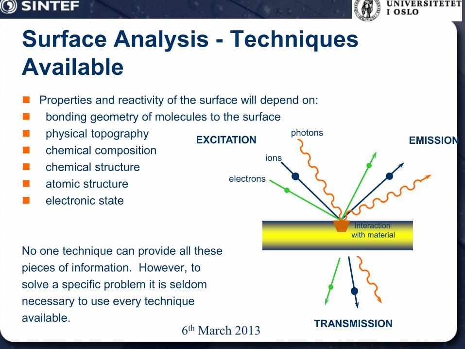
Properties and reactivity of the surface will depend on: bonding geometry of molecules to the surface physical topography chemical composition chemical structure atomic structure electronic state
No one technique can provide all these pieces of information. However, to solve a specific problem it is seldom necessary to use every technique available.
photons
ions
electrons
EMISSION
TRANSMISSION
Interaction with material
EXCITATION
Surface Analysis - Techniques Available
6th March 2013 5
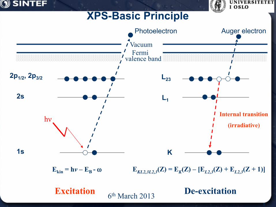
hν
Photoelectron
2p1/2, 2p3/2
2s
1s
Ekin = hν – EB - ω
L23
L1
K
EKL2,3L2,3(Z) = EK(Z) – [EL2,3(Z) + EL2,3(Z + 1)]
Internal transition
(irradiative)
Auger electron
XPS-Basic Principle
valence band Fermi
Vacuum
De-excitation Excitation
6th March 2013 6
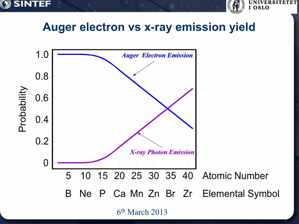
Auger electron vs x-ray emission yield
5
B Ne P Ca Mn Zn Br Zr
10 15 20 25 30 35 40 Atomic Number
Elemental Symbol
0
0.2
0.4
0.6
0.8
1.0
Pro
babi
lity
Auger Electron Emission
X-ray Photon Emission
6th March 2013 7
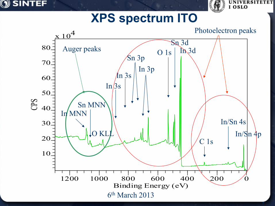
XPS spectrum ITO x 104
10
20
30
40
50
60
70
80
CPS
1200 1000 800 600 400 200 0Binding Energy (eV)
In 3d Sn 3d
O 1s
In 3p Sn 3p
In 3s In 3s
In MNN Sn MNN
O KLL
Auger peaks
Photoelectron peaks
In/Sn 4p In/Sn 4s
C 1s
6th March 2013 8
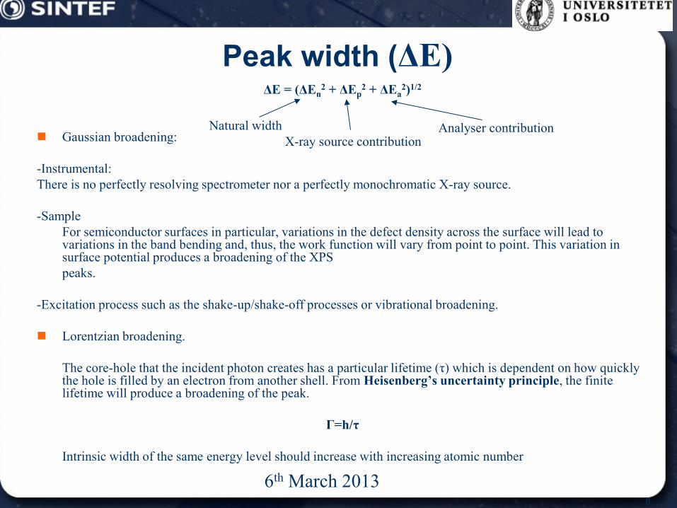
Peak width (ΔE)
ΔE = (ΔEn2 + ΔEp
2 + ΔEa2)1/2
Gaussian broadening: -Instrumental: There is no perfectly resolving spectrometer nor a perfectly monochromatic X-ray source. -Sample For semiconductor surfaces in particular, variations in the defect density across the surface will lead to
variations in the band bending and, thus, the work function will vary from point to point. This variation in surface potential produces a broadening of the XPS
peaks. -Excitation process such as the shake-up/shake-off processes or vibrational broadening.
Lorentzian broadening. The core-hole that the incident photon creates has a particular lifetime (τ) which is dependent on how quickly
the hole is filled by an electron from another shell. From Heisenberg’s uncertainty principle, the finite lifetime will produce a broadening of the peak.
Γ=h/τ
Intrinsic width of the same energy level should increase with increasing atomic number
Natural width X-ray source contribution
Analyser contribution
6th March 2013 9
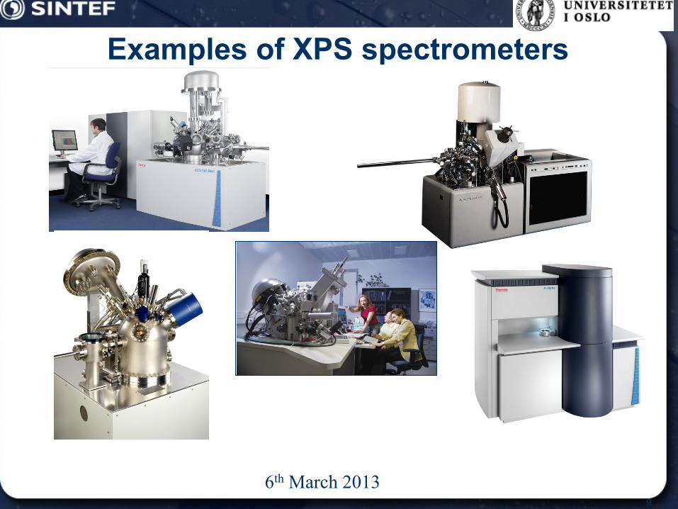
Examples of XPS spectrometers
6th March 2013 10
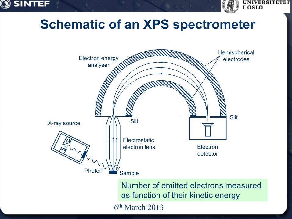
Schematic of an XPS spectrometer
Number of emitted electrons measured as function of their kinetic energy
Al
X-ray source
Electrostatic electron lens Electron
detector
Electron energy analyser
Sample e- Photon
Slit
Hemispherical electrodes
Slit
6th March 2013 11
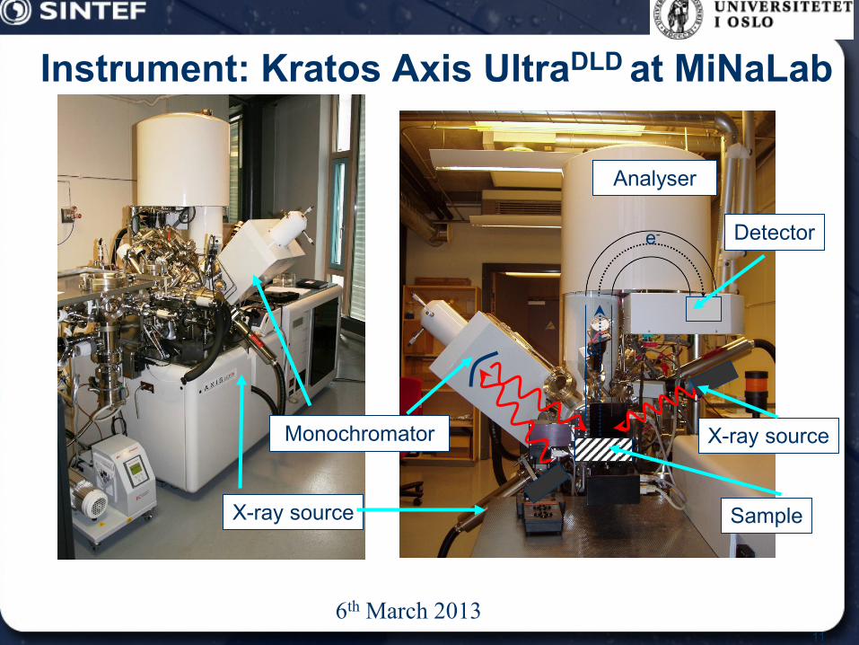
Instrument: Kratos Axis UltraDLD at MiNaLab
Analyser
Monochromator
Sample
Detector
X-ray source
X-ray source
e-
e-
6th March 2013
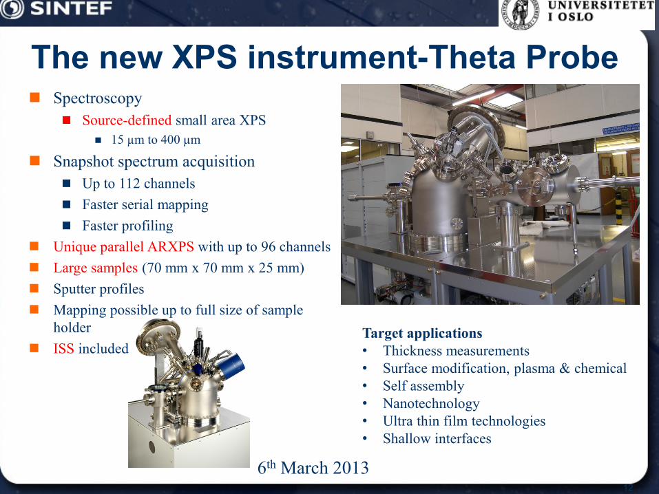
The new XPS instrument-Theta Probe
12
Spectroscopy Source-defined small area XPS
15 µm to 400 µm
Snapshot spectrum acquisition Up to 112 channels Faster serial mapping Faster profiling
Unique parallel ARXPS with up to 96 channels Large samples (70 mm x 70 mm x 25 mm) Sputter profiles Mapping possible up to full size of sample
holder ISS included
Target applications • Thickness measurements • Surface modification, plasma & chemical • Self assembly • Nanotechnology • Ultra thin film technologies • Shallow interfaces
6th March 2013 13
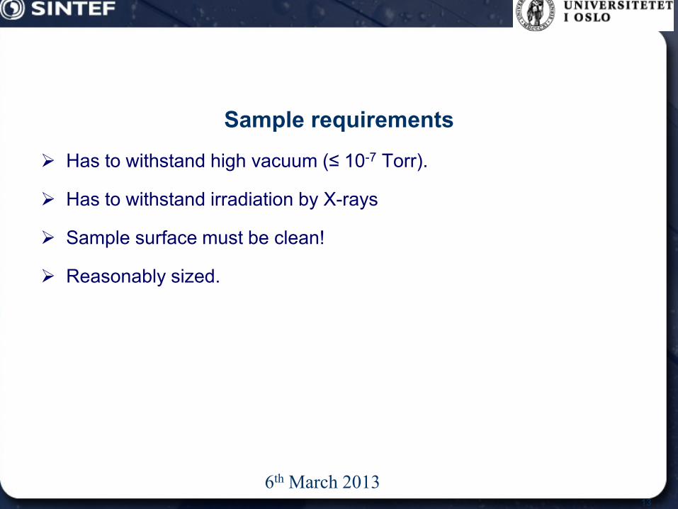
Sample requirements
Has to withstand high vacuum (≤ 10-7 Torr).
Has to withstand irradiation by X-rays
Sample surface must be clean!
Reasonably sized.
6th March 2013 14
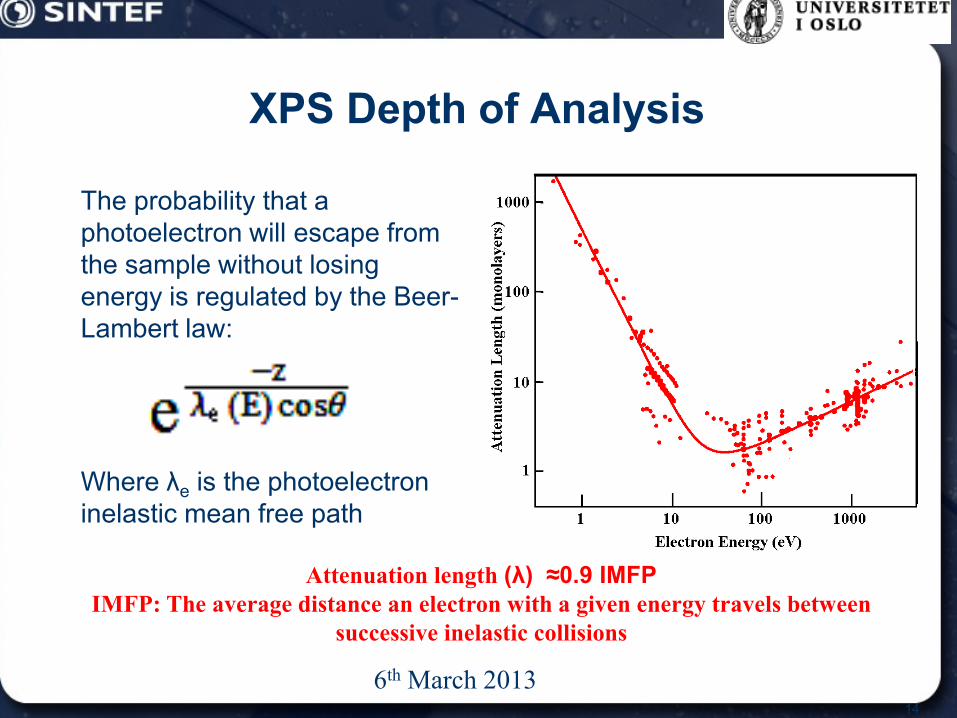
XPS Depth of Analysis
The probability that a photoelectron will escape from the sample without losing energy is regulated by the Beer-Lambert law:
Where λe is the photoelectron inelastic mean free path
Attenuation length (λ) ≈0.9 IMFP IMFP: The average distance an electron with a given energy travels between
successive inelastic collisions

6th March 2013 15
Features of the XPS spectrum Primary structure
- Core level photoelectron peaks (atom excitation) - Valence band spectra - CCC, CCV, CVV Auger peaks (atom de-excitation)
Secondary structure
- X-ray satellites and ghosts - Shake up and shake off satellites - Plasmon loss features - Background (slope)
6th March 2013 16
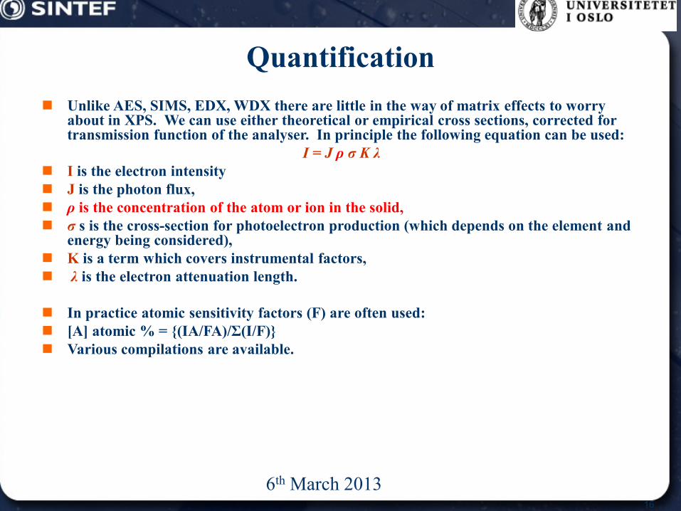
Quantification Unlike AES, SIMS, EDX, WDX there are little in the way of matrix effects to worry
about in XPS. We can use either theoretical or empirical cross sections, corrected for transmission function of the analyser. In principle the following equation can be used:
I = J ρ σ K λ I is the electron intensity J is the photon flux, ρ is the concentration of the atom or ion in the solid, σ s is the cross-section for photoelectron production (which depends on the element and
energy being considered), K is a term which covers instrumental factors, λ is the electron attenuation length.
In practice atomic sensitivity factors (F) are often used: [A] atomic % = {(IA/FA)/Σ(I/F)} Various compilations are available.
6th March 2013 17
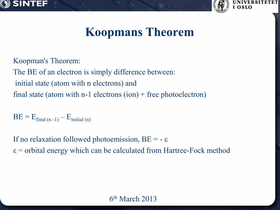
Koopmans Theorem
Koopman's Theorem: The BE of an electron is simply difference between: initial state (atom with n electrons) and final state (atom with n-1 electrons (ion) + free photoelectron) BE = Efinal (n -1) – Einitial (n)
If no relaxation followed photoemission, BE = - ε ε = orbital energy which can be calculated from Hartree-Fock method
6th March 2013 18
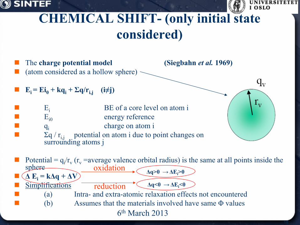
CHEMICAL SHIFT- (only initial state considered)
The charge potential model (Siegbahn et al. 1969) (atom considered as a hollow sphere)
Ei = Ei0 + kqi + Σq/ri,j (i≠j)
Ei BE of a core level on atom i Ei0 energy reference qi charge on atom i Σq / ri,j potential on atom i due to point changes on
surrounding atoms j
Potential = qi/rv (rv =average valence orbital radius) is the same at all points inside the sphere
Δ Ei = kΔq + ΔV Simplifications (a) Intra- and extra-atomic relaxation effects not encountered (b) Assumes that the materials involved have same Φ values
oxidation
reduction
Δq>0 → ΔEi>0
Δq<0 → ΔEi<0
6th March 2013 19
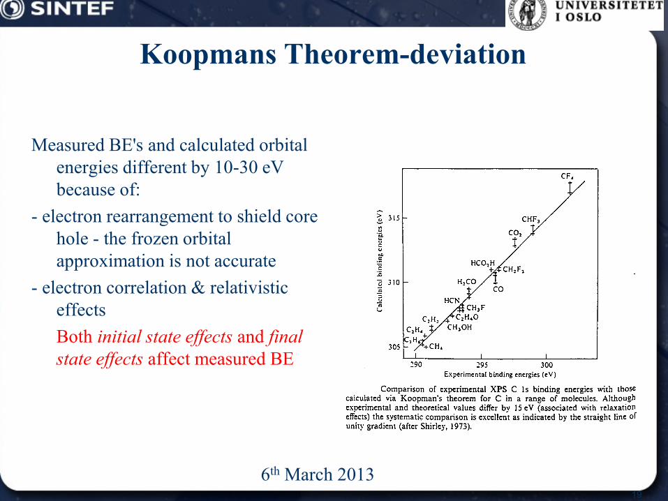
Koopmans Theorem-deviation
Measured BE's and calculated orbital energies different by 10-30 eV because of:
- electron rearrangement to shield core hole - the frozen orbital approximation is not accurate
- electron correlation & relativistic effects
Both initial state effects and final state effects affect measured BE
6th March 2013
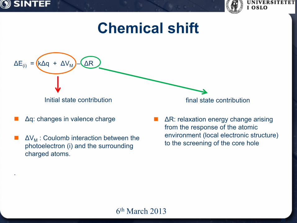
Chemical shift
ΔE(i) = kΔq + ΔVM – ΔR
Initial state contribution
Δq: changes in valence charge
ΔVM : Coulomb interaction between the photoelectron (i) and the surrounding charged atoms.
.
final state contribution
ΔR: relaxation energy change arising from the response of the atomic environment (local electronic structure) to the screening of the core hole
20
6th March 2013
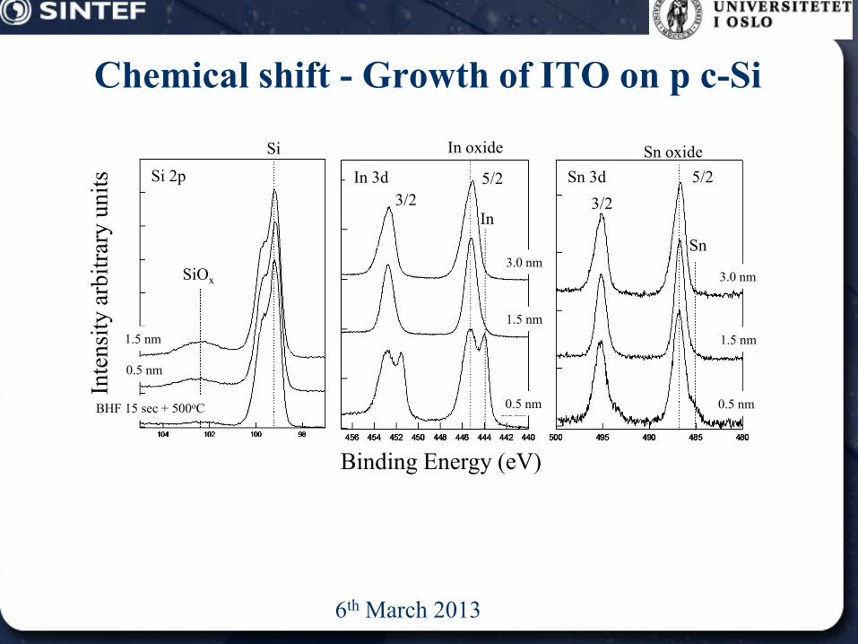
Chemical shift - Growth of ITO on p c-Si
Inte
nsity
arb
itrar
y un
its
Binding Energy (eV)
SiOx
Si In oxide
In
Sn oxide
Sn
3/2 3/2 5/2 5/2
1.5 nm
0.5 nm
BHF 15 sec + 500oC 0.5 nm
1.5 nm
3.0 nm
0.5 nm
1.5 nm
3.0 nm
Si 2p In 3d Sn 3d
6th March 2013 22
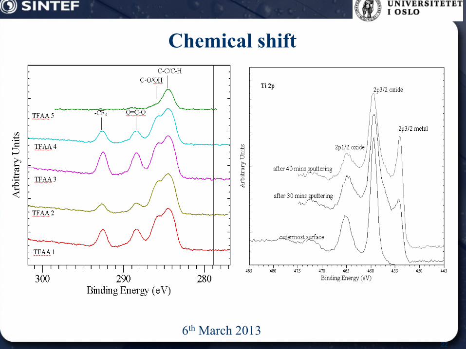
Chemical shift
6th March 2013 23
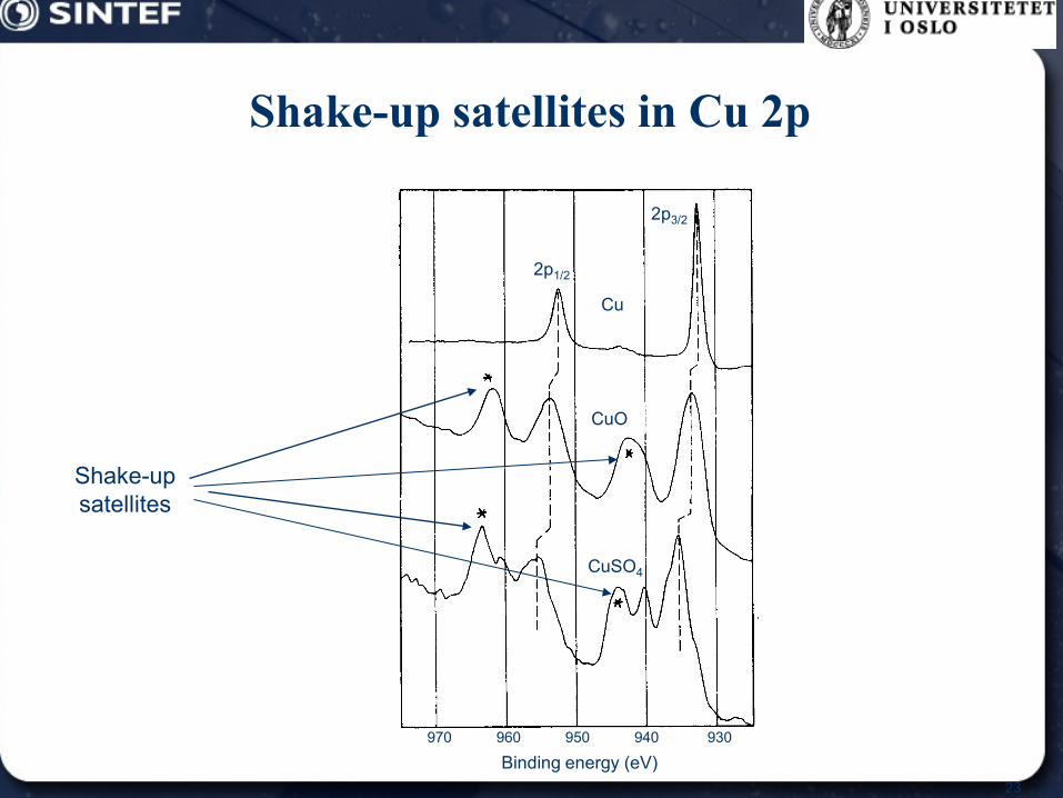
Shake-up satellites in Cu 2p
Shake-up satellites
2p3/2
2p1/2
Cu
CuO
CuSO4
Binding energy (eV) 970 960 950 940 930
6th March 2013 24
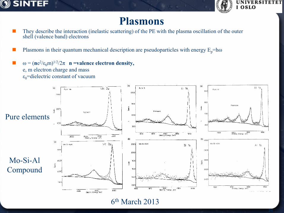
Plasmons
Pure elements
Mo-Si-Al Compound
They describe the interaction (inelastic scattering) of the PE with the plasma oscillation of the outer shell (valence band) electrons
Plasmons in their quantum mechanical description are pseudoparticles with energy Ep=hω
ω = (ne2/ε0m)1/2/2π n =valence electron density, e, m electron charge and mass ε0=dielectric constant of vacuum
6th March 2013 25
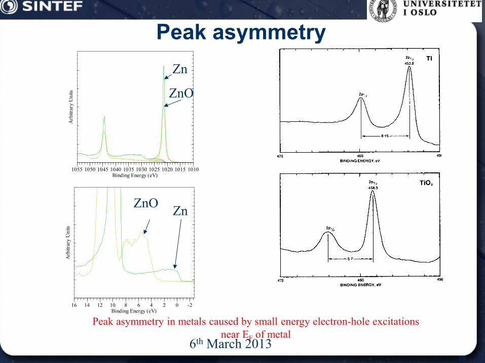
Peak asymmetry
Peak asymmetry in metals caused by small energy electron-hole excitations near EF of metal
Arb
itrar
y U
nits
16 14 12 10 8 6 4 2 0 -2Binding Energy (eV)
Arb
itrar
y U
nits
1055 1050 1045 1040 1035 1030 1025 1020 1015 1010Binding Energy (eV)
Zn
ZnO
Zn ZnO

6th March 2013 26
Depth profile with ion sputtering
Use of an ion gun to erode the sample surface and re-analyse Enables layered structures to be investigated Investigations of interfaces Depth resolution improved by: Low beam energies Small ion beam sizes Sample rotation
SnO2
Sn
Depth 500 496 492 488 484 480
6th March 2013 27
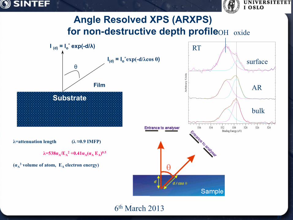
Angle Resolved XPS (ARXPS) for non-destructive depth profile
Substrate
I(d) = Io*exp(-d/λcos θ) θ
Film
I (d) = Io* exp(-d/λ)
λ=attenuation length (λ ≈0.9 IMFP)
λ=538αA/EA2 +0.41αA(αA EA)0.5
(αA
3 volume of atom, EA electron energy)
Arb
itra
ry U
nits
536 534 532 530 528 526 524Binding Energy (eV)
OH oxide
bulk
AR
surface
RT

6th March 2013 28
XPS-Check list Depth of analysis ~ 5nm All elements except H and He Readily quantified (limit ca. 0.1 at%) All materials (vacuum compatible) Chemical/electronic state information -Identification of chemical states -Reflection of electronic changes to the atomic potential Compositional depth profiling by -ARXPS (ultra thin film <10 nm), -change of the excitation energy -choose of different spectral areas -sputtering Ultra thin film thickness measurement Analysis area mm2 to 10 micrometres
6th March 2013 29
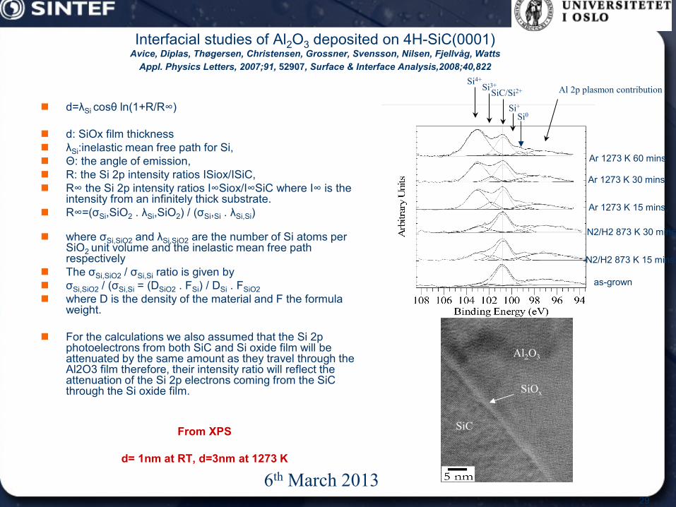
Interfacial studies of Al2O3 deposited on 4H-SiC(0001) Avice, Diplas, Thøgersen, Christensen, Grossner, Svensson, Nilsen, Fjellvåg, Watts
Appl. Physics Letters, 2007;91, 52907, Surface & Interface Analysis,2008;40,822
d=λSi cosθ ln(1+R/R∞)
d: SiOx film thickness λSi:inelastic mean free path for Si, Θ: the angle of emission, R: the Si 2p intensity ratios ISiox/ISiC, R∞ the Si 2p intensity ratios I∞Siox/I∞SiC where I∞ is the
intensity from an infinitely thick substrate. R∞=(σSi,SiO2 . λSi,SiO2) / (σSi,Si . λSi,Si)
where σSi,SiO2 and λSi,SiO2 are the number of Si atoms per
SiO2 unit volume and the inelastic mean free path respectively
The σSi,SiO2 / σSi,Si ratio is given by σSi,SiO2 / (σSi,Si = (DSiO2 . FSi) / DSi . FSiO2 where D is the density of the material and F the formula
weight.
For the calculations we also assumed that the Si 2p photoelectrons from both SiC and Si oxide film will be attenuated by the same amount as they travel through the Al2O3 film therefore, their intensity ratio will reflect the attenuation of the Si 2p electrons coming from the SiC through the Si oxide film.
From XPS
d= 1nm at RT, d=3nm at 1273 K
Si0
Si4+ Si3+ SiC/Si2+ Al 2p plasmon contribution
Si+
SiC
Al2O3
SiOx
as-grown
N2/H2 873 K 15 mins
N2/H2 873 K 30 mins
Ar 1273 K 15 mins, Ar 1273 K 30 mins Ar 1273 K 60 mins
6th March 2013 30
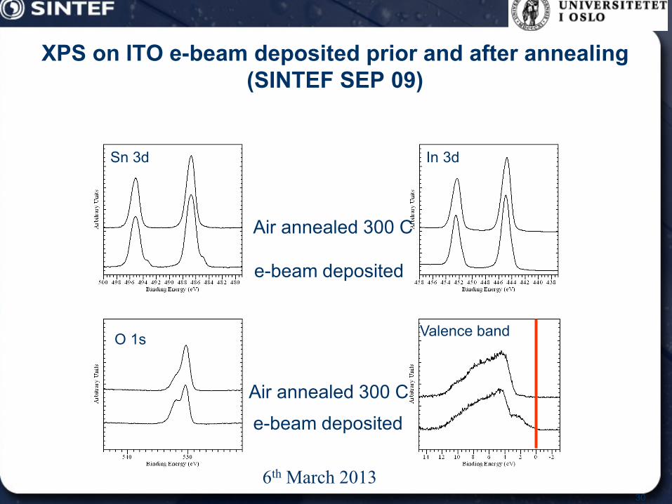
XPS on ITO e-beam deposited prior and after annealing (SINTEF SEP 09)
Sn 3d In 3d
O 1s Valence band
e-beam deposited
e-beam deposited
Air annealed 300 C
Air annealed 300 C
6th March 2013 31
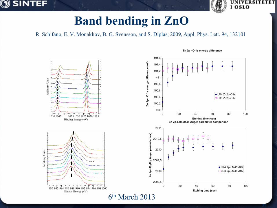
Band bending in ZnO R. Schifano, E. V. Monakhov, B. G. Svensson, and S. Diplas, 2009, Appl. Phys. Lett. 94, 132101
A
rbitr
ary
Uni
ts
1050 1045 1035 1030 1025 1020 1015Binding Energy (eV)
Arb
itrar
y U
nits
980 982 984 986 988 990 992 994 996 998 1000Kinetic Energy (eV)
Zn 2p - O 1s energy difference
490
490,2
490,4
490,6
490,8
491
491,2
491,4
491,6
0 20 40 60 80 100
Etching time (sec)
Zn 2
p - O
1s
ener
gy d
iffer
ence
(eV)
LR4 Zn2p-O1sLR3 Zn2p-O1s
Zn 2p-LM45M45 Auger parameter comparison
2008,5
2009
2009,5
2010
2010,5
2011
0 20 40 60 80 100
Etching time (sec)
Zn 2
p-LM
45M
45 A
uger
par
amet
er (e
V)
LR4 2p-LM45M45LR3 2p-LM45M45
6th March 2013 32
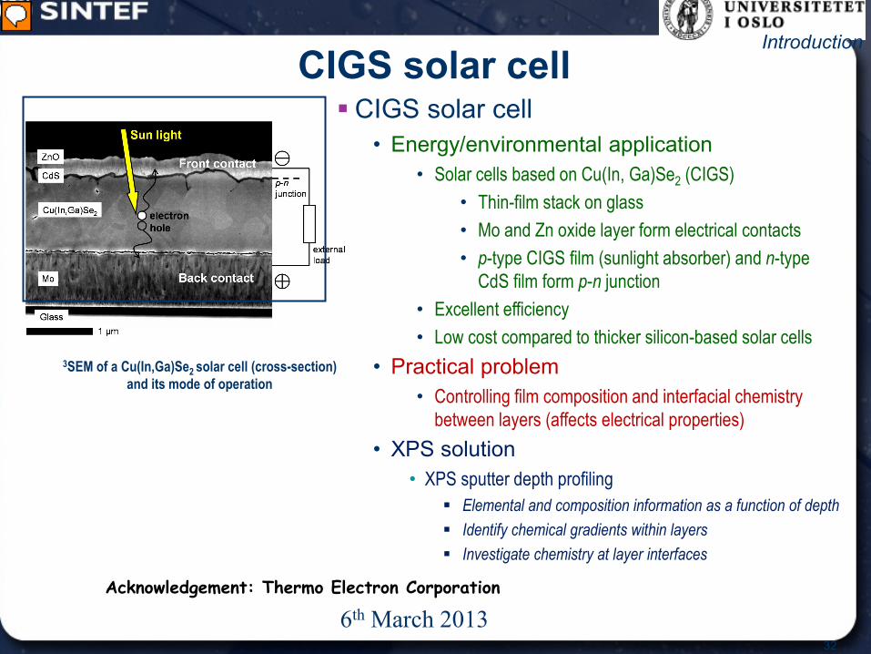
CIGS solar cell Introduction
3SEM of a Cu(In,Ga)Se2 solar cell (cross-section) and its mode of operation
CIGS solar cell • Energy/environmental application
• Solar cells based on Cu(In, Ga)Se2 (CIGS) • Thin-film stack on glass • Mo and Zn oxide layer form electrical contacts • p-type CIGS film (sunlight absorber) and n-type
CdS film form p-n junction • Excellent efficiency • Low cost compared to thicker silicon-based solar cells
• Practical problem • Controlling film composition and interfacial chemistry
between layers (affects electrical properties) • XPS solution
• XPS sputter depth profiling Elemental and composition information as a function of depth Identify chemical gradients within layers Investigate chemistry at layer interfaces
Acknowledgement: Thermo Electron Corporation
6th March 2013 33
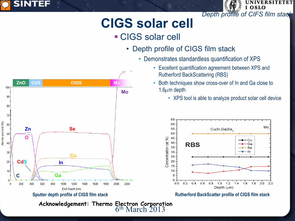
CIGS solar cell Depth profile of CIFS film stack
CIGS solar cell • Depth profile of CIGS film stack
• Demonstrates standardless quantification of XPS • Excellent quantification agreement between XPS and
Rutherford BackScattering (RBS) • Both techniques show cross-over of In and Ga close to
1.6µm depth • XPS tool is able to analyze product solar cell device
Zn
O
Se
Cu
Ga
In
Mo
CdS
C
Sputter depth profile of CIGS film stack Rutherford BackScatter profile of CIGS film stack
Acknowledgement: Thermo Electron Corporation
6th March 2013 34
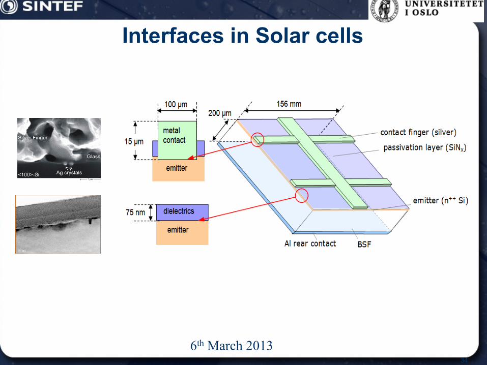
Interfaces in Solar cells
6th March 2013 35
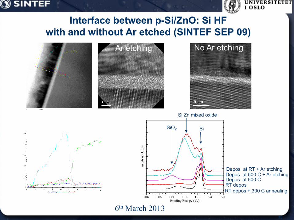
Interface between p-Si/ZnO: Si HF with and without Ar etched (SINTEF SEP 09)
SiO2
Si Zn mixed oxide
Si
RT depos + 300 C annealing RT depos Depos at 500 C Depos at 500 C + Ar etching Depos at RT + Ar etching
No Ar etching Ar etching
6th March 2013
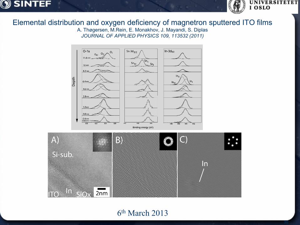
Elemental distribution and oxygen deficiency of magnetron sputtered ITO films A. Thøgersen, M.Rein, E. Monakhov, J. Mayandi, S. Diplas
JOURNAL OF APPLIED PHYSICS 109, 113532 (2011)
36

6th March 2013 37
Thank you for your attention