Embed Size (px)
Citation preview

WPC1604 Qi Developer Forum Circuit Design Considerations
Dave Wilson 24-August-2016

PAGE 2
Overview
Getting Started
Basics The Qi Advantage for Circuit Design
Practical Design Issues
Practical Implementation Issues
Worldwide Agency and Government Requirements

PAGE 3
- Electromagnetic Induction - Magnetic Induction - Direct Induction
Magnetic field mostly contained in between ferrite shielding
- Magnetic Resonance - Resonant Transformer - Resonant Inductive Coupling
Magnetic field radiates outward - not shielded
Start: Consider Wireless Power Delivery Methods
- Capacitive Coupling - Radio Waves - Acoustic Waves

PAGE 4
The Basic Air Core Transformer Idea
Coupling coefficient ‘k’ impacts mutual inductance M ● k influenced by turns ratio, ferrite area/thickness, and the space between the coils
(k = 0.5 – 0.8 ideally)
V1 V2

PAGE 5
Study Likely Coil Size Ratios and Separation Distances
•Coupling between coils •–Distance (z) between coils •–Ratio of diameters (D2 / D) of the two coils •–Physical orientation ••Quality factor •–Ratio of inductance to resistance •–Geometric mean of two Q factors ••Uncoupled field has no losses ••Near field allows TX to “see” RX

PAGE 6
Consider Coil Alignment Possibilities

PAGE 7
Work Through All of the Efficiency Tradeoffs
Mag Eff
Tx Eff Rx Eff
System Efficiency = ηSYSTEM=POL/PIN

PAGE 8
Start Circuit Design After Deciding…
What is a good operating voltage? What is the minimum / maximum power delivery required?
How should the system respond to load changes?
What about thermal design, EMI, and efficiency? How large is the “good” working area for power delivery?
and should the design be single-coil or multi-coil ?? Do a resonant type design or a non-resonant type design?

PAGE 9
The Problem with this Design Approach . . .
There is a truly infinite matrix of design decisions and tradeoffs before even starting a circuit design Following these rules requires a very deep understanding of physics, flux
flow/capture, simulation/modeling of systems, and so-on A good design can take a very long time to make, and a fully working and
tested system using discrete components may also be very expensive A completely new design based on the basic physics is unlikely to be
interoperable with any other independently designed system

PAGE 10
The WPC Qi System Advantage
“Best of both worlds” solution using partially resonant magnetic induction ● Loosely coupled air-core transformer ● Useable air-gap working distance of about 3mm – 8mm (depending on transmitter type)
dB/dt
I
Partially resonant Transmitter LC tank
Partially resonant Receiver LC tank
Air gap

PAGE 11
Simplified Design Using WPC Qi Systems
Qi certified Transmitter designs are fully worked out, including detailed specification of all operational parameters and the physical coil design Receiver designs are similarly worked out, but in a way that enables the
designer to choose/modify/make a Receiver coil that perfectly fits the design Because Qi is a robust interoperability standard, IC makers have invested to
make single-chip solutions that completely eliminate most of the design work

PAGE 12
WPC Qi-Based Circuit Design Flow
Transmitter Design ● Choose the pre-defined Qi Transmitter type that best matches the application ● Choose from an IC vendor a chip solution that best meets the requirements for cost,
efficiency, EMC emissions, component count, etc. ● Follow closely the IC vendor guidelines for system implementation
Receiver Design ● Choose from an IC vendor a chip solution that best meets the requirements for cost,
efficiency, EMC emissions, component count, physical area/height, etc. ● Choose a receiver coil that best matches the application and IC vendor guidance ● Follow closely the IC vendor guidelines for system implementation

PAGE 13
WHAT COULD POSSIBLY GO WRONG ??
Actually there are a few things, and system circuit designers are still very important

PAGE 14
WPC Power Transmitter Basic Topology
Primary coil (Lp) + serial resonance capacitor (Cp) DC-to-AC Inverter: e.g. half bridge (shown below) or full-bridge Power level is controlled by changing transmitter operating frequency, operatin
duty cycle, and/or bridge supply voltage. Power is controlled by the Receiver which is the master of the transmitter Multiple coil solutions function the same as single-coil with the “best” coil
selected by the transmitter before beginning interoperation with the Receiver
Power Conversion
Cp
Lp
+
-
Half Bridge
Power Conversion
Multiplexer
Lp
+
-
Lm
Cm
Freq Freq
Single Coil Multiple Coils

PAGE 15
WPC Power Receiver Basic Topology
Secondary coil (Ls) Serial resonance capacitor (Cs) for efficient power transfer Parallel resonance capacitor (Cd) for required alternative method to detect
presence of a Receiver device by making 1MHz resonance Important Note: The Cd value must be chosen to work with the selected Receiver coil while on a non-operating transmitter to accurately decide the capacitor value. This will help transmitters that use this method to work well. AC-to-DC Rectifier: full bridge (diode, or switched) + capacitor Output switch for disconnecting the load
Power Pickup Unit
Ls
Cs
Cd C
Load

PAGE 16
WPC Communication (Modulation)
Receiver modulates load by method of Amplitude Shift Keying (ASK) ● Switch on/off modulation resistor (Rm), or ● Switch on/off modulation capacitor (Cm)
Transmitter demodulates Receiver information by ● Sensing primary coil current (Ip) and/or ● Sensing primary coil voltage (Vp)
Transmitter modulates the frequency of the coil power signal to send information to Receiver ● Receiver measures Tx coil drive frequency to demodulate Transmitter information
Transmitter
Cp
Lp
+
-
Receiver
Cd
Ls
Cs
C Rm
Modulation Modulation
Cm
Ip Vp
Load
Power
Note: Demodulated amplitude ranges from about 800mVpp to 10mVpp

PAGE 17
WPC Communication (Data-Format) Speed: 2 Kbit/s Bit-encoding: bi-phase Byte encoding: Start-bit, 8bit data, parity-bit, stop-bit
Packet Structure ● Preamble (typically 4 - 11bits) ● Header (1 Byte)
• Indicates packet type and message length ● Message (1 .. 27 Byte)
• One complete message per packet • Payload for control
● Checksum (1 Byte)
1 0 1 0 1 1 0 0
0.5ms
b0 b1 b2 b3 b4 b5 b6 b7
Star
t
Stop
Parit
y
Preamble Header Message Checksum
PAGE 18
Now Finally the Actual Very Important Circuit Design Work

PAGE 19
Example of Circuit Design Special Cases
Single-Chip Transmitter
with Integrated
Power Transistors
Main Coil should be
approved type in certified
product
Caps Must Be COG Type
Precision Current-Sensing Type Resistor
Coil peak detector and demodulation circuit all closely the same as IC vendor recommended
Bulk and bypass capacitors should closely follow IC
vendor recommended
Current-Sense circuit should closely follow IC vendor recommended

PAGE 20
Design Checklist: Component Selection (1)
If the transmitter uses external power transistors for the bridge driver, these must be carefully and fully designed-in ● IC vendor may specify gate drive characteristics, switching time, etc. ● Typically the designer can choose the device on-resistance for the best cost decision ● Passive components tied to the power transistor may need to be adjusted according to the
IC vendor recommendations depending on the properties of the selected transistor
The transmitter coil is best selected by choosing a coil that is used in an actual design that has passed all WPC requirements. Alternative coils could have issues to be checked carefully, such as: ● Improper inductance value for the specified transmitter type ● Higher than expected coil resistance (could cause FOD or Guaranteed Power issue) ● Thinner than specified ferrite material (could cause FOD and/or Guaranteed Power issue) ● Low quality ferrite material that could be lossy, become easily saturated, etc.
COG capacitors in the power circuit are a must and should not be substituted. For example, using instead an X7R type in a Tx-A11 design will add about 400mW heat loss into the capacitors. This can cause FOD and Guaranteed Power problems and could cause failure of the capacitors. This is from the partial resonance in the LC tank making a big circulating current

PAGE 21
Design Checklist: Component Selection (2)
If the transmitter uses an external current sensing resistor, this is very important for the FOD and other measurements. So a true current-sense type resistor should be used with the accuracy as specified by the IC vendor
Bypass and “bulk” capacitors that on both the Transmitter and Receiver should not be made less than or different from the IC vendor recommendation. And if these are low-cost ceramic type, then the “derating” of the actual capacitance value should have careful engineering attention so that the effective capacitance value is the same as what the IC vendor recommends. (Note: The IC vendor may already have taken into account such derating assuming a particular type of capacitor is used.) Additionally, capacitors can make acoustic noise, and this can vary depending on the construction and material type of the capacitor.
If there are any demodulation passive components in the transmitter or modulation components in the Receiver, the type and tolerance recommendation of the IC vendor should be followed. These may be critically balanced for best performance, and changes can cause unreliable communication issues between Rx and Tx.
PAGE 22
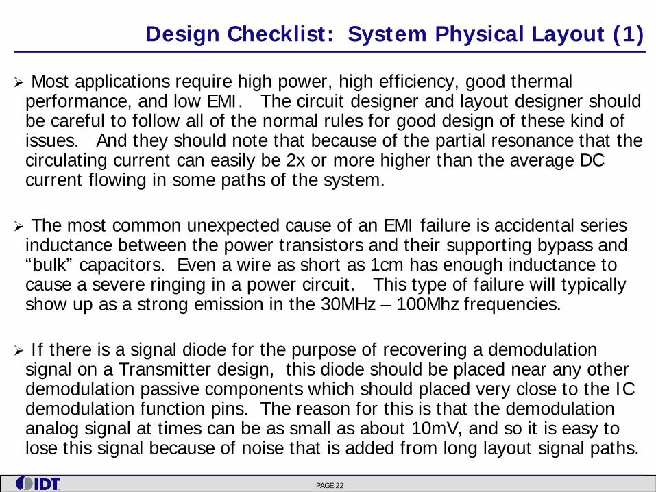
Design Checklist: System Physical Layout (1)
Most applications require high power, high efficiency, good thermal performance, and low EMI. The circuit designer and layout designer should be careful to follow all of the normal rules for good design of these kind of issues. And they should note that because of the partial resonance that the circulating current can easily be 2x or more higher than the average DC current flowing in some paths of the system.
The most common unexpected cause of an EMI failure is accidental series inductance between the power transistors and their supporting bypass and “bulk” capacitors. Even a wire as short as 1cm has enough inductance to cause a severe ringing in a power circuit. This type of failure will typically show up as a strong emission in the 30MHz – 100Mhz frequencies.
If there is a signal diode for the purpose of recovering a demodulation signal on a Transmitter design, this diode should be placed near any other demodulation passive components which should placed very close to the IC demodulation function pins. The reason for this is that the demodulation analog signal at times can be as small as about 10mV, and so it is easy to lose this signal because of noise that is added from long layout signal paths.
PAGE 23
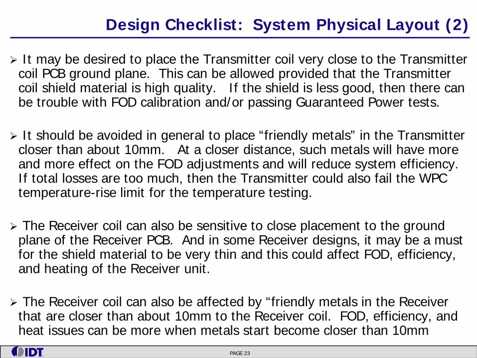
Design Checklist: System Physical Layout (2)
It may be desired to place the Transmitter coil very close to the Transmitter coil PCB ground plane. This can be allowed provided that the Transmitter coil shield material is high quality. If the shield is less good, then there can be trouble with FOD calibration and/or passing Guaranteed Power tests.
It should be avoided in general to place “friendly metals” in the Transmitter closer than about 10mm. At a closer distance, such metals will have more and more effect on the FOD adjustments and will reduce system efficiency. If total losses are too much, then the Transmitter could also fail the WPC temperature-rise limit for the temperature testing.
The Receiver coil can also be sensitive to close placement to the ground plane of the Receiver PCB. And in some Receiver designs, it may be a must for the shield material to be very thin and this could affect FOD, efficiency, and heating of the Receiver unit.
The Receiver coil can also be affected by “friendly metals in the Receiver that are closer than about 10mm to the Receiver coil. FOD, efficiency, and heat issues can be more when metals start become closer than 10mm
PAGE 24
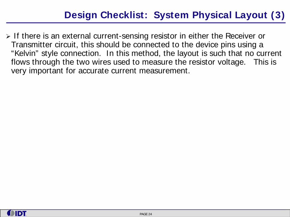
Design Checklist: System Physical Layout (3)
If there is an external current-sensing resistor in either the Receiver or Transmitter circuit, this should be connected to the device pins using a “Kelvin” style connection. In this method, the layout is such that no current flows through the two wires used to measure the resistor voltage. This is very important for accurate current measurement.

PAGE 25
Example of Circuit Layout Special Cases
Single-Chip Transmitter
with Integrated
Power Transistors
Main Coil
DC Power Supply path to Caps <20mm for
Good EMI Performance
Precision Current-Sensing Resistor “Kelvin” type connection
path between sensing resistor and IC pins
Demodulation circuit all placed close to the IC
demodulation pins

PAGE 26
Worldwide Agency and Government Compliance
WPC certification and specifications do not address worldwide requirements for EMI/EMC, efficiency, materials, etc. And these specifications can be strongly different depending on the country, or in cases, even depending on a smaller region inside a country. Designers must have good knowledge of all such requirements where they plan for their product to be sold. Examples:
● CISPR-22 ● FCC Part-15, Part-18 ● EN-300-330-1 (magnetic emissions) ● California “Green” efficiency requirements ● Regional “Green” materials requirements for safety ● Regional “Green” materials requirements for recycling

PAGE 27
Supplemental Information

PAGE 28
Foreign Object Heating WPC Compliance Test
Three Reference Test Foreign Objects are Defined in Detail ● Object #1: 15mm dia steel disk with integrated thermocouple ● Object #2: 20mm dia aluminum alloy disk with integrated thermocouple ● Object #3: 20mm dia aluminum foil disk with integrated thermocouple ● Test frames and spacers are also defined for placing/holding test objects on Tx surface
Synopsis of Test Procedure ● Follow various specified placements and sequencing ● If Tx refuses to go to power transfer with the object present, this is passing ● If Tx terminates power transfer within various times/metrics, this is passing ● If Tx continues power transfer, but object temperature remains below limit, this is passing ● Pass if objects #1, #2 < 60-C heating and #3 < 80-C heating
Example Cross Section View Example Plan View 15mm dia object 17.9mm dia
for comparison

PAGE 29
FOD Power Loss Method – Step 1
• Transmitter determines actual power available to Rx • Measure input power “Pin” • Account for all known Tx losses “Pptloss” • Determine power available at Tx coil surface “Ppt”

PAGE 30
FOD Power Loss Method – Step 2
• Receiver determines actual power available from Tx • Measure “Pout” • Account for all known Rx losses “Pprloss” • Determine power available at Tx coil surface “Ppr”

PAGE 31
FOD Power Loss Method – Step 3
• Transmitter determines if there is an unexplained loss • Receiver reports Ppr as “Received Power” • Transmitter calculates Ppt-Ppr • If more power is lost than allowed, then FOD

PAGE 32
Q-Measurement Method
Normally, for efficiency, the Tx has a very high “Q”, which is the Quality Factor. When the coil is very low resistance and losses in the Tx PCB, COG capacitors, and transistors is very small, then the Q-factor will be very high
When there is any loss of energy from the Tx coil such as by foreign metal, friendly metal, or power taken by the Rx, then this reduces the “Q” of the Tx.
In the Q-Measurement method, the Tx uses information from the Rx to decide if the Q-factor with the Rx present is the amount expected.
If there is some FOD, the Q-factor measurement will be lower than expected and so Tx will decide there is an FOD case

PAGE 33
Circuit Design Requirements for FOD Measurement
Tx and Rx must be able to accurately measure their power (or voltage and current) at the correct time and with sufficient bandwidth. These parameters will vary with different IC designs and measurement methods used by those ICs. Typical implementations have some low pass passive circuit to smooth the measured value to avoid aliasing. Additionally, for Q-measurement, the Transmitter must accurately
determine its peak coil voltage at the correct time and with sufficient bandwidth. Typical implementations have some low pass passive circuit to smooth the measured value to avoid aliasing.

PAGE 34
Calibrating the Tx FOD for Loss Method
Calibration of the Tx for the loss method is done by: 1. Step through the entire power range from zero to maximum 2. Measure the known losses of the Tx by comparing the available output
power to the actual DC input power 3. Make a table of the known losses inside the Tx 4. Use the loss table to determine the available output power for all
possible cases Note: For this to work, the output must be measured very accurately, and the only way to do this at this time is to use a specialized test tool such as made by Nok9.

PAGE 35
Calibrating the Rx FOD for Loss Method
Calibration of the Rx for the loss method is done by: 1. Step through the entire power range from zero to maximum 2. Measure the known losses of the Rx by comparing the available output
power to the actual power available from the Tx coil 3. Make a table of the known losses inside the Rx 4. Use the loss table to determine the actual power available to Rx based
on the measured output power from the Rx 5. Add a “loss allowance” so that there is some margin for error when the
Tx does the loss calculation to determine FOD or not Note: For this to work, the power available from Tx must be measured very accurately, and the only way to do this at this time is to use a specialized test tool such as made by Nok9
LOSS ALLOWANCE TABLE FROM WPC SPECIFICATIONS

PAGE 36
Calibrating the Q Method
The Tx must know from its memory the Q-factor of its overall design. This can be a self-calibration, but it must be done at a time when it is 100% guaranteed there is nothing on the Tx surface. (So this cannot simply be done in the field.)
The Rx must know its effect on the Nok9 MPA1 Tx Q-factor. This must be measured in the lab on the Nok9 tool at a time it is 100% guaranteed there is no foreign object present. The Rx must remember this value in its memory and report this value during the startup sequence with Tx


