Embed Size (px)
Citation preview
© 2006 Texas Instruments Inc, Slide 1
Working with ADCs, OAsand the MSP430
Bonnie BakerHPA Senior Applications Engineer
Texas Instruments
© 2006 Texas Instruments Inc, Slide 2
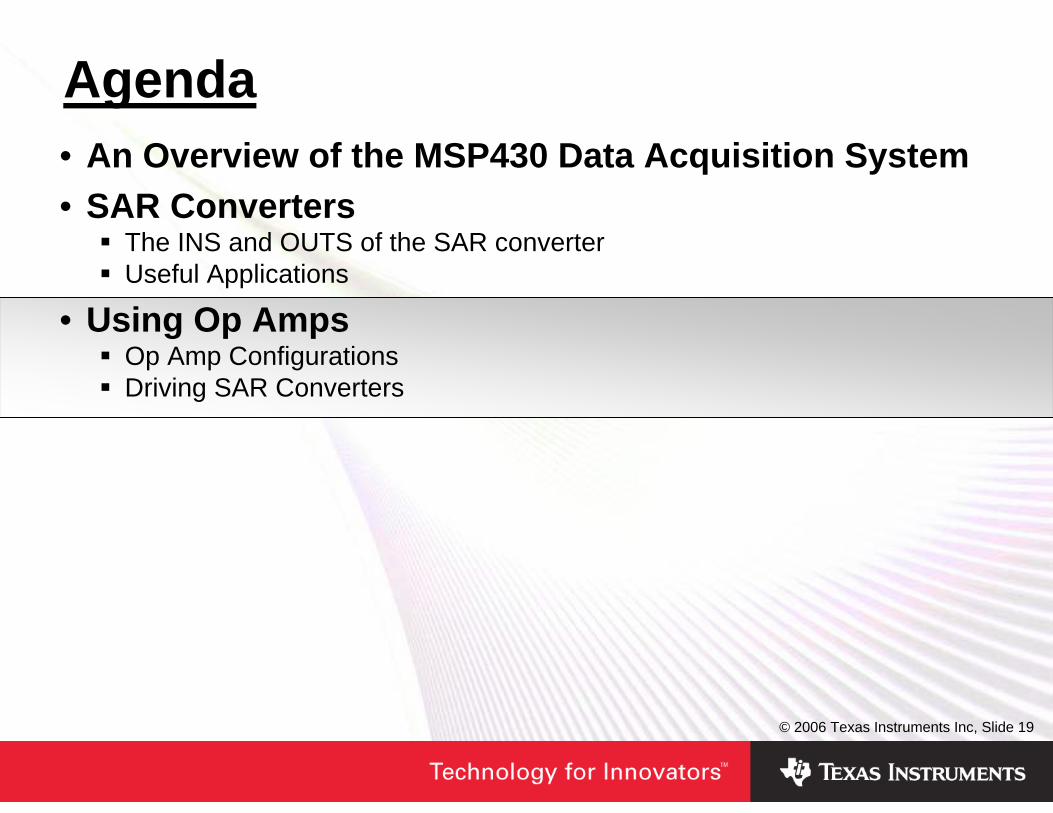
Agenda• An Overview of the MSP430 Data Acquisition System • SAR Converters
The INS and OUTS of the SAR converterUseful Applications
• Using Op Amps Op Amp ConfigurationsDriving SAR Converters
© 2006 Texas Instruments Inc, Slide 3
OPAMPOP
AMPMUXMUX FILTERFILTER A/DA/D
μ Cμ C
D/AD/APOWERAMP
POWERAMP
REFREF
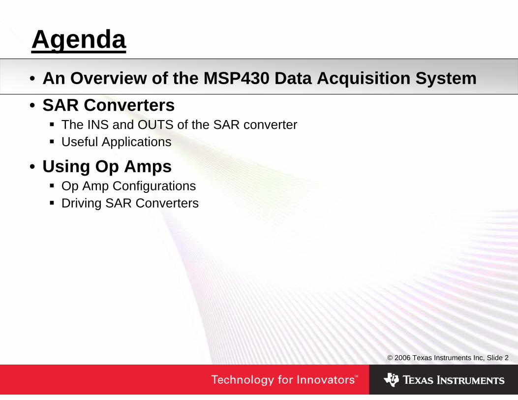
Where to Find ADCs and Op Amps
Anti-Alias FilterBand-pass FilterProgrammable Gain AmpInstrumentation AmpA/D Converter Driver
Sensor InterfaceVoltage Reference SourceBufferGainDifference AmplifierInstrumentation AmplifierFilterLevel Shift
Voltage Reference Source
Actuator DriverLine Driver4-20mA Driver
Voltage Reference SourceDDS Synthesis
Valve
© 2006 Texas Instruments Inc, Slide 4
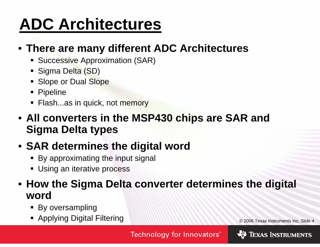
ADC Architectures• There are many different ADC Architectures
Successive Approximation (SAR)Sigma Delta (SD)Slope or Dual SlopePipelineFlash...as in quick, not memory
• All converters in the MSP430 chips are SAR and Sigma Delta types
• SAR determines the digital wordBy approximating the input signal Using an iterative process
• How the Sigma Delta converter determines the digital word
By oversamplingApplying Digital Filtering
© 2006 Texas Instruments Inc, Slide 5
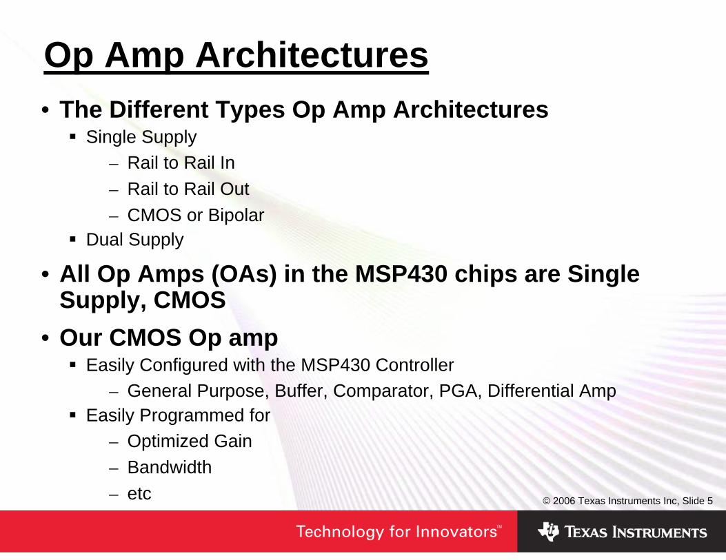
Op Amp Architectures• The Different Types Op Amp Architectures
Single Supply– Rail to Rail In– Rail to Rail Out– CMOS or Bipolar
Dual Supply
• All Op Amps (OAs) in the MSP430 chips are Single Supply, CMOS
• Our CMOS Op amp Easily Configured with the MSP430 Controller
– General Purpose, Buffer, Comparator, PGA, Differential AmpEasily Programmed for
– Optimized Gain– Bandwidth– etc
© 2006 Texas Instruments Inc, Slide 6
Agenda• An Overview of the MSP430 Data Acquisition System • SAR Converters
The INS and OUTS of the SAR converterUseful Applications
• Using Op Amps Op Amp ConfigurationsDriving SAR Converters
© 2006 Texas Instruments Inc, Slide 7
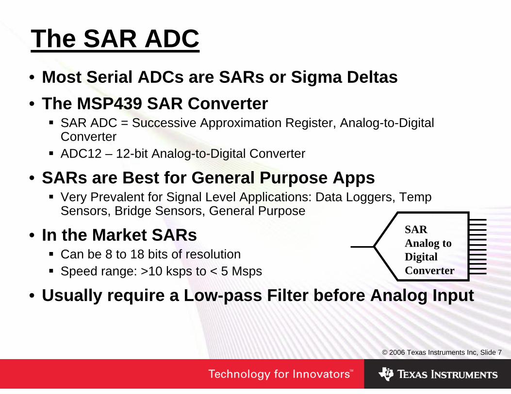
The SAR ADC • Most Serial ADCs are SARs or Sigma Deltas• The MSP439 SAR Converter
SAR ADC = Successive Approximation Register, Analog-to-Digital ConverterADC12 – 12-bit Analog-to-Digital Converter
• SARs are Best for General Purpose AppsVery Prevalent for Signal Level Applications: Data Loggers, TempSensors, Bridge Sensors, General Purpose
• In the Market SARsCan be 8 to 18 bits of resolutionSpeed range: >10 ksps to < 5 Msps
• Usually require a Low-pass Filter before Analog Input
SARAnalog to Digital Converter

© 2006 Texas Instruments Inc, Slide 8
System Integration Using an A/D
InputSignalSource
DAC or PWM
Filter
Analog to Digital Converter
FilterAmpMicro-ControllerEngine
Output
SARAnalog to Digital Converter
FilterAmp
MSP430
© 2006 Texas Instruments Inc, Slide 9
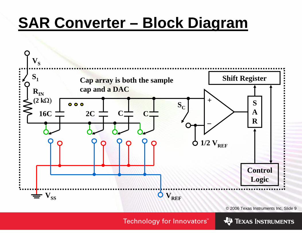
VS
16C 2C C C
VREF
1/2 VREF
SC+
_
SAR
Control Logic
RIN(2 kΩ)
Shift Register
VSS
Cap array is both the sample cap and a DAC
S1
SAR Converter – Block Diagram

© 2006 Texas Instruments Inc, Slide 10
Successive Approximation Concept
Analog inputVIN
FS
0
1/4FS
1/2FS
3/4FS
TEST MSB
TEST MSB -1
TEST LSB
TEST MSB -2
Bit = 1
Bit = 0Bit = 1 Bit = 0
Digital Output Code = 1010DAC OutputTime
© 2006 Texas Instruments Inc, Slide 11
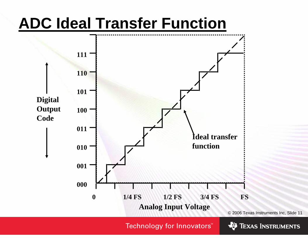
000
001
010
011
100
101
110
111
DigitalOutputCode
Ideal transferfunction
FS1/2 FS 3/4 FS1/4 FS0
ADC Ideal Transfer Function
Analog Input Voltage
© 2006 Texas Instruments Inc, Slide 12
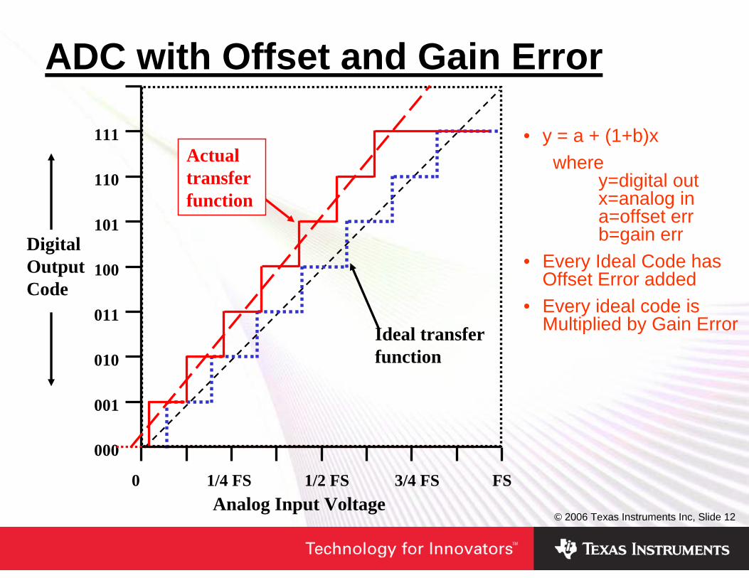
000
001
010
011
100
101
110
111
DigitalOutputCode
Ideal transferfunction
FS1/2 FS 3/4 FS1/4 FS0
ADC with Offset and Gain Error
• y = a + (1+b)x where
y=digital outx=analog ina=offset errb=gain err
• Every Ideal Code has Offset Error added
• Every ideal code is Multiplied by Gain Error
Actualtransferfunction
Analog Input Voltage
© 2006 Texas Instruments Inc, Slide 13
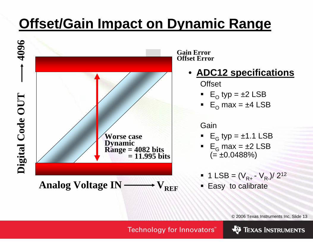
Analog Voltage IN
Dig
ital C
ode
OU
T
VREF
4096 Gain Error
Offset Error
Worse case DynamicRange = 4082 bits
= 11.995 bits
Offset/Gain Impact on Dynamic Range
• ADC12 specificationsOffset
EO typ = ±2 LSBEO max = ±4 LSB
GainEG typ = ±1.1 LSBEG max = ±2 LSB (= ±0.0488%)
1 LSB = (VR+ - VR-)/ 212
Easy to calibrate
© 2006 Texas Instruments Inc, Slide 14
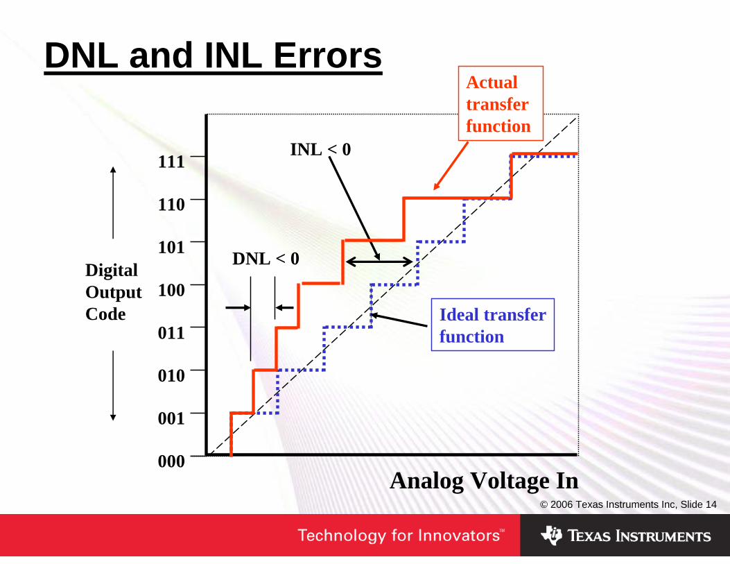
DNL and INL Errors
000
001
010
011
100
101
110
111
Ideal transferfunction
Actualtransferfunction
INL < 0
DigitalOutputCode
DNL < 0
Analog Voltage In

© 2006 Texas Instruments Inc, Slide 15
Analog Voltage IN
Dig
ital C
ode
OU
T
VREF
4096
INL, DNLrms ADC Noise
INL/DNL/Noise Impact on Dynamic Range • ADC12 specifications
DNL error ED max = ±1.7 LSBINL errorEI max = ±1 LSB1 LSB = (VR+ - VR-)/ 212
• INL, DNL and Noise errors move across the entire range
• Impacts the Effective Number of Bits (ENOB)
• Not Easily calibrated• Effects Accuracy
© 2006 Texas Instruments Inc, Slide 16
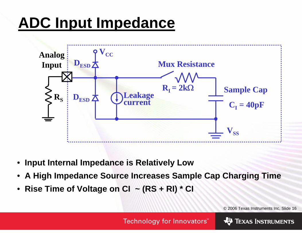
ADC Input Impedance
• Input Internal Impedance is Relatively Low• A High Impedance Source Increases Sample Cap Charging Time• Rise Time of Voltage on CI ~ (RS + RI) * CI
RI = 2kΩ
CI = 40pF
Analog Input
Sample Cap
Mux Resistance
Leakage current
VCC
VSS
RS DESD
DESD
© 2006 Texas Instruments Inc, Slide 17
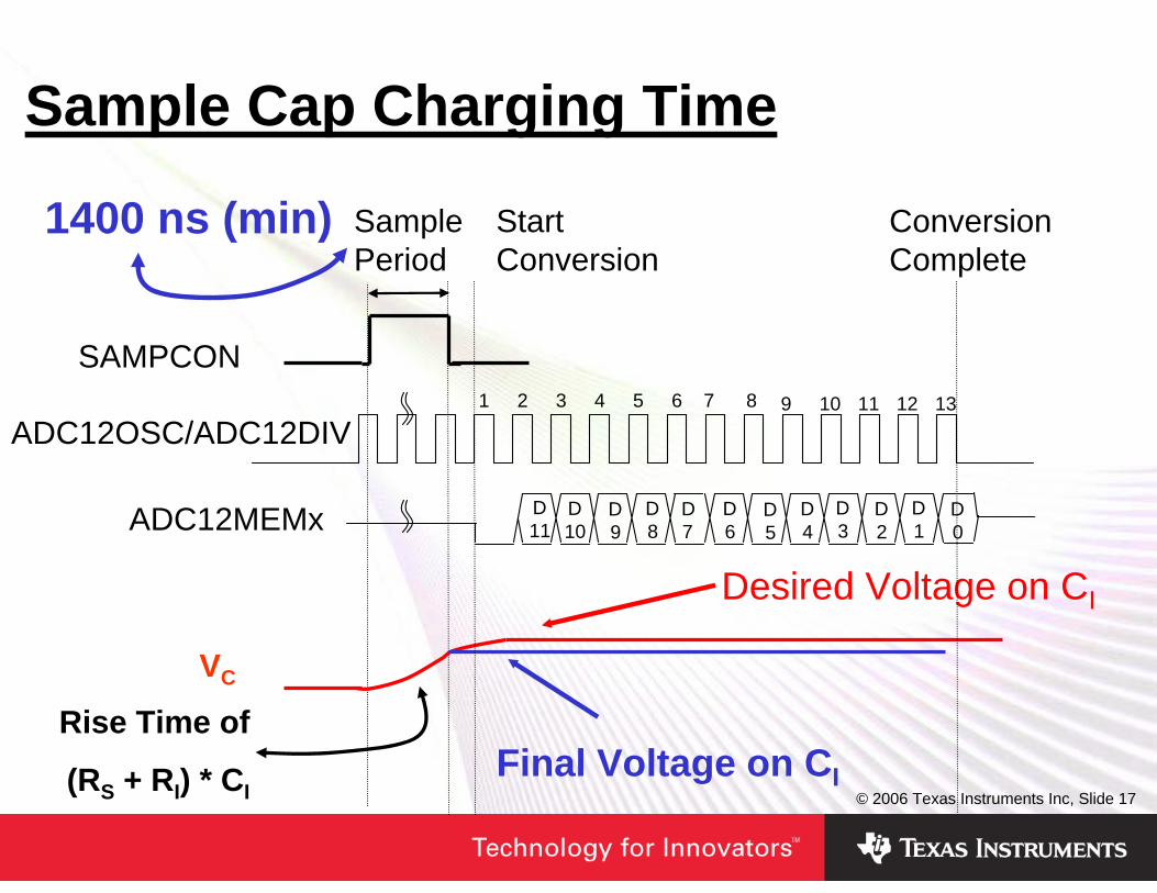
Sample Cap Charging Time
1 2 3 4 5 6 7 8 9 10 11 12
SAMPCON
ADC12OSC/ADC12DIV
VC
SamplePeriod
ADC12MEMx 910 8 7 6 5 4 3 2 1 011DD D D D D D D D D DD
Final Voltage on CI
Desired Voltage on CI
13
StartConversion
ConversionComplete
1400 ns (min)
Rise Time of
(RS + RI) * CI
© 2006 Texas Instruments Inc, Slide 18
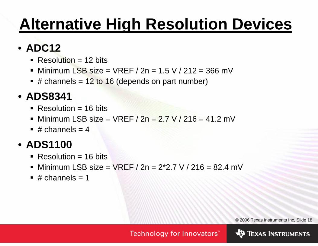
Alternative High Resolution Devices• ADC12
Resolution = 12 bitsMinimum LSB size = VREF / 2n = 1.5 V / 212 = 366 mV# channels = 12 to 16 (depends on part number)
• ADS8341Resolution = 16 bitsMinimum LSB size = VREF / 2n = 2.7 V / 216 = 41.2 mV# channels = 4
• ADS1100Resolution = 16 bitsMinimum LSB size = VREF / 2n = 2*2.7 V / 216 = 82.4 mV# channels = 1
© 2006 Texas Instruments Inc, Slide 19
Agenda• An Overview of the MSP430 Data Acquisition System • SAR Converters
The INS and OUTS of the SAR converterUseful Applications
• Using Op Amps Op Amp ConfigurationsDriving SAR Converters
© 2006 Texas Instruments Inc, Slide 20
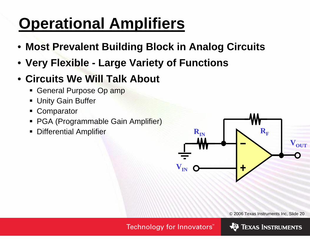
Operational Amplifiers• Most Prevalent Building Block in Analog Circuits• Very Flexible - Large Variety of Functions• Circuits We Will Talk About
General Purpose Op ampUnity Gain BufferComparatorPGA (Programmable Gain Amplifier)Differential Amplifier
VOUT
VIN
RFRIN

© 2006 Texas Instruments Inc, Slide 21
OPAMPOP
AMPMUXMUX FILTERFILTER A/DA/D
μ Cμ C
D/AD/APOWERAMP
POWERAMP
REFREF
Where to Find Op Amps
Anti-Alias FilterBand-pass FilterProgrammable Gain AmpInstrumentation AmpA/D Converter Driver
Sensor InterfaceVoltage Reference SourceBufferGainDifference AmplifierInstrumentation AmplifierFilterLevel Shift
Voltage Reference Source
Actuator DriverLine Driver4-20mA Driver
Voltage Reference SourceDDS Synthesis
Valve
© 2006 Texas Instruments Inc, Slide 22
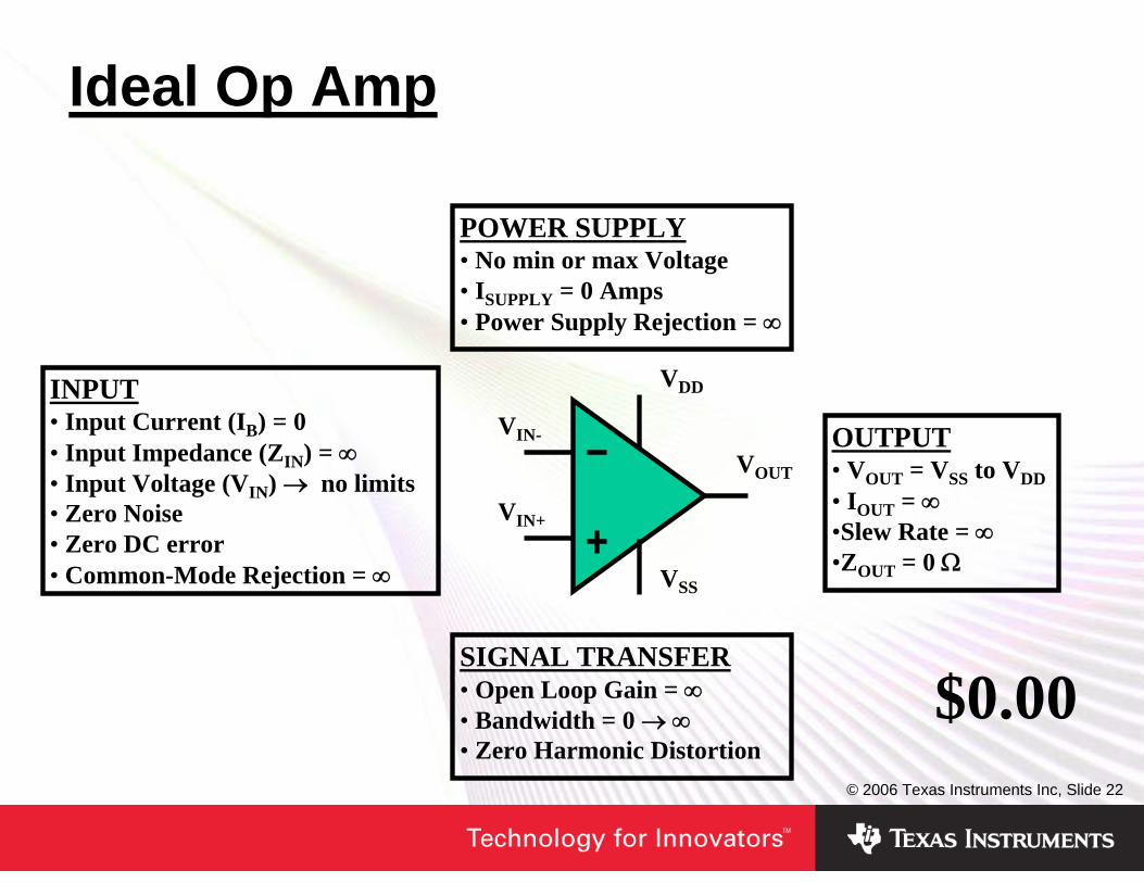
Ideal Op Amp
POWER SUPPLY• No min or max Voltage• ISUPPLY = 0 Amps• Power Supply Rejection = ∞
OUTPUT• VOUT = VSS to VDD• IOUT = ∞•Slew Rate = ∞•ZOUT = 0 Ω
SIGNAL TRANSFER• Open Loop Gain = ∞• Bandwidth = 0 →∞• Zero Harmonic Distortion
INPUT• Input Current (IB) = 0• Input Impedance (ZIN) = ∞• Input Voltage (VIN) → no limits• Zero Noise• Zero DC error• Common-Mode Rejection = ∞
$0.00
VDD
VSS
VIN-
VIN+
VOUT
© 2006 Texas Instruments Inc, Slide 23
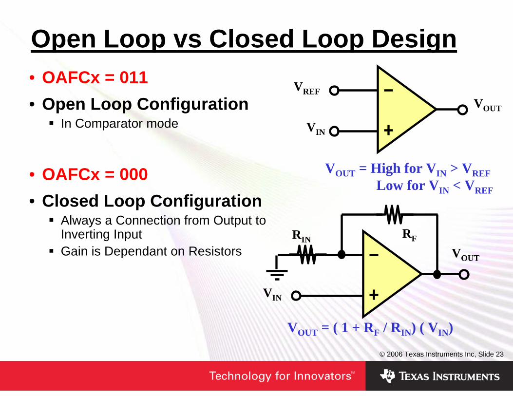
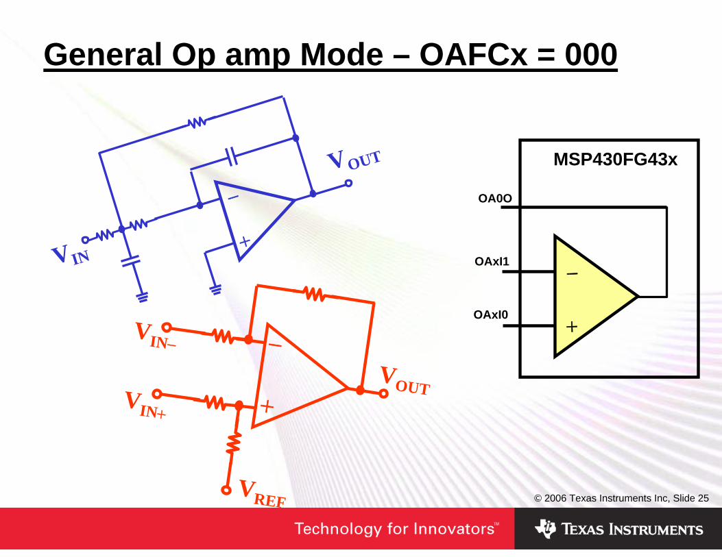
Open Loop vs Closed Loop Design• OAFCx = 011• Open Loop Configuration
In Comparator mode
• OAFCx = 000• Closed Loop Configuration
Always a Connection from Output to Inverting InputGain is Dependant on Resistors
VOUT = ( 1 + RF / RIN) ( VIN)
VOUT = High for VIN > VREFLow for VIN < VREF
VOUT
VIN
VREF
VOUT
VIN
RFRIN
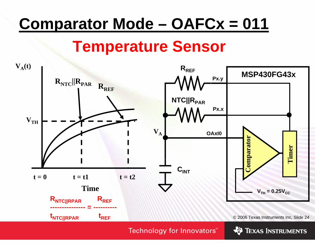
© 2006 Texas Instruments Inc, Slide 24
CINT
RREF
NTC||RPAR
MSP430FG43x
VTH
VA(t)
Timet = 0 t = t1 t = t2
RNTC||RPAR RREF
Comparator Mode – OAFCx = 011
Px.y
Px.x
OAxI0VA
Com
para
tor
Tim
er
RNTC||RPAR RREF--------------- = ----------tNTC||RPAR tREF
VTH = 0.25VCC
Temperature Sensor
© 2006 Texas Instruments Inc, Slide 25
OA0O
OAxI1
OAxI0
MSP430FG43x
General Op amp Mode – OAFCx = 000
+
−
VIN
VOUT
+
−
+
−VIN−
VOUT
VREF
VIN+
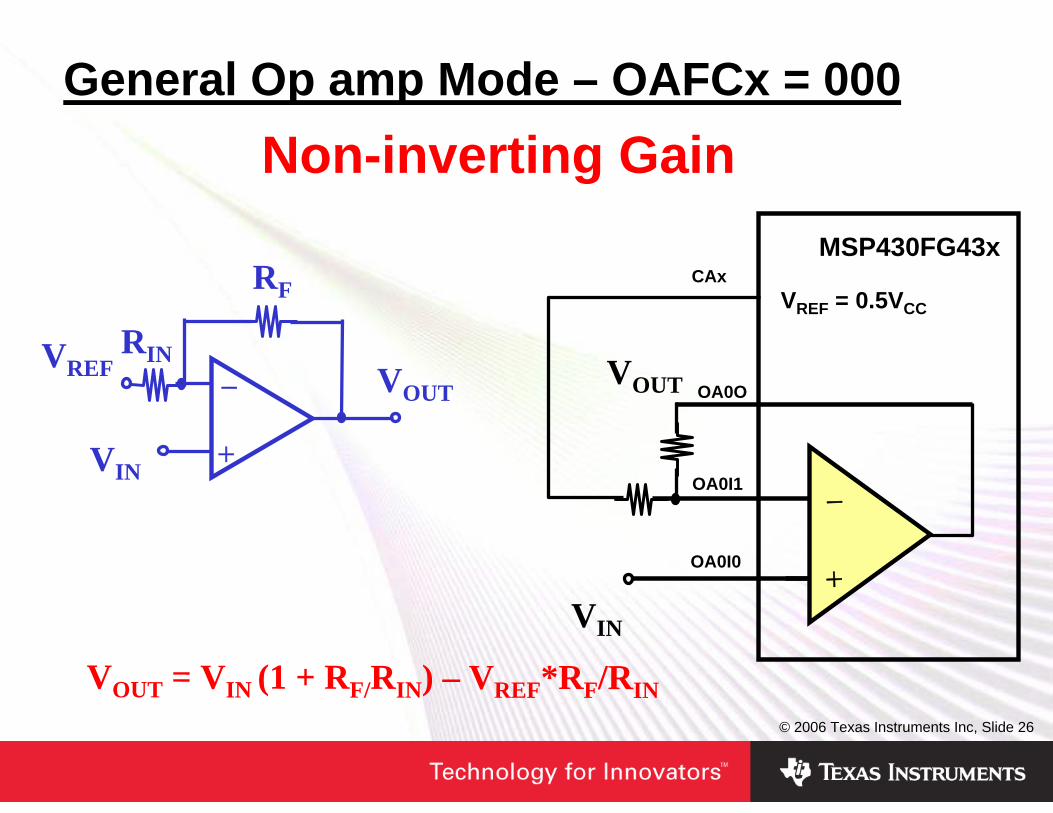
© 2006 Texas Instruments Inc, Slide 26
OA0O
OA0I1
OA0I0
MSP430FG43x
General Op amp Mode – OAFCx = 000
+
− VOUT
+
−
VOUT = VIN (1 + RF/RIN) – VREF*RF/RIN
VIN
VOUT
RF
RINVREF
Non-inverting Gain
VIN
VREF = 0.5VCC
CAx
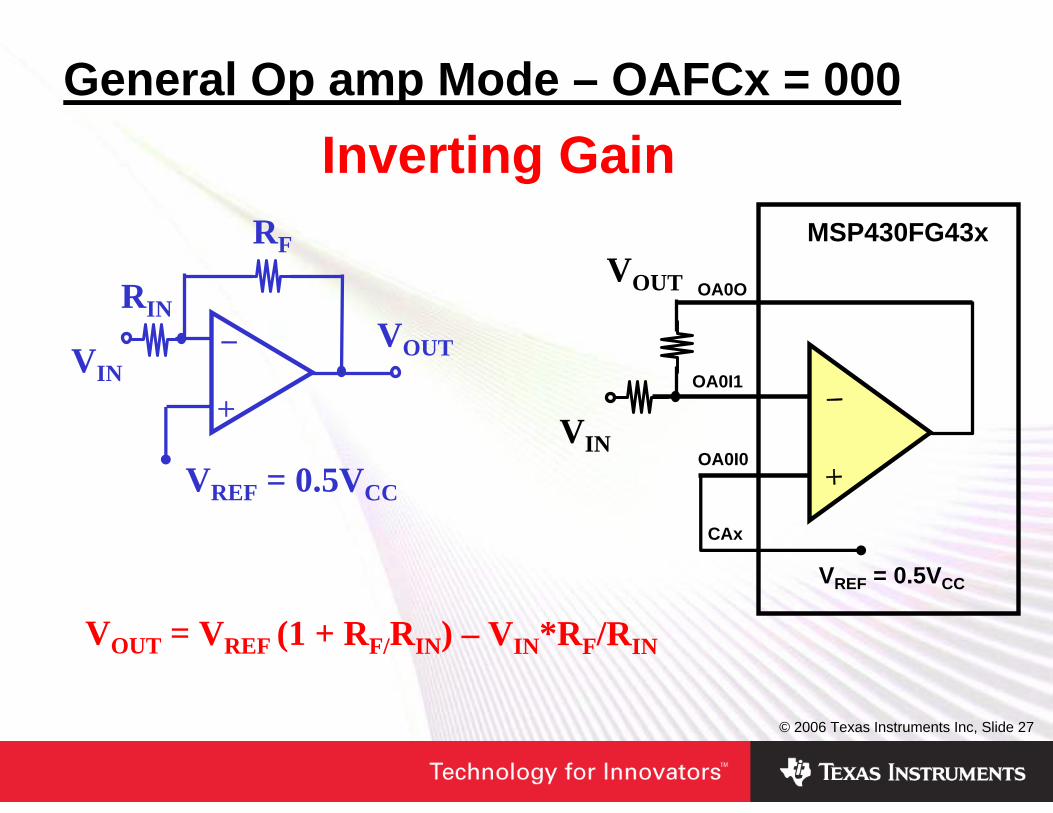
© 2006 Texas Instruments Inc, Slide 27
OA0O
OA0I1
MSP430FG43x
General Op amp Mode – OAFCx = 000
+
−VINVOUT
+
−
VOUT = VREF (1 + RF/RIN) – VIN*RF/RIN
VREF = 0.5VCC
VIN
VOUT
RF
RIN
VREF = 0.5VCC
Inverting Gain
OA0I0
CAx
© 2006 Texas Instruments Inc, Slide 28
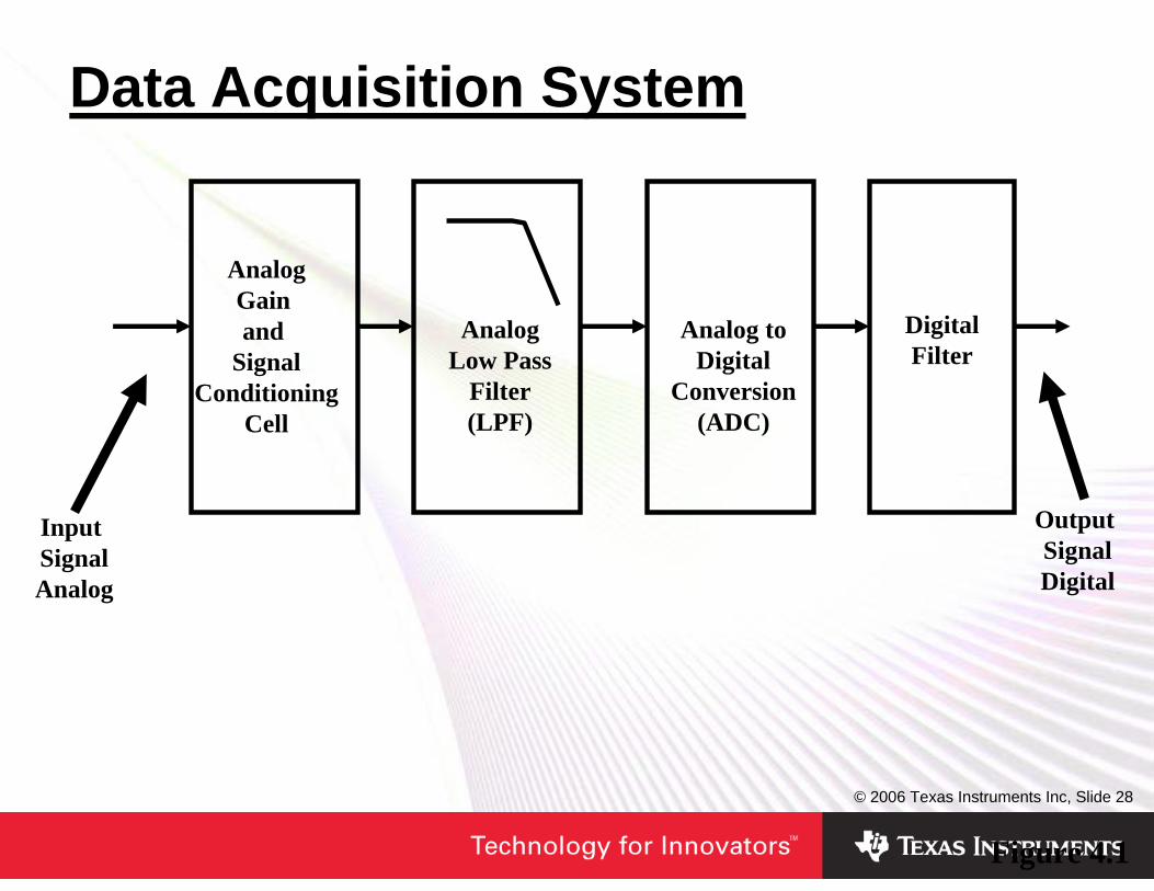
AnalogGain and
SignalConditioning
Cell
AnalogLow Pass
Filter(LPF)
Analog toDigital
Conversion(ADC)
DigitalFilter
Data Acquisition System
Input SignalAnalog
Output SignalDigital
Figure 4.1

© 2006 Texas Instruments Inc, Slide 29
Noise Reduction with a Low Pass Filter
Noise Reduction or Anti-aliasing Filter
ADC12
C22
R23
+
-
OA
R21 R22
C21
VREF
VIN
© 2006 Texas Instruments Inc, Slide 30
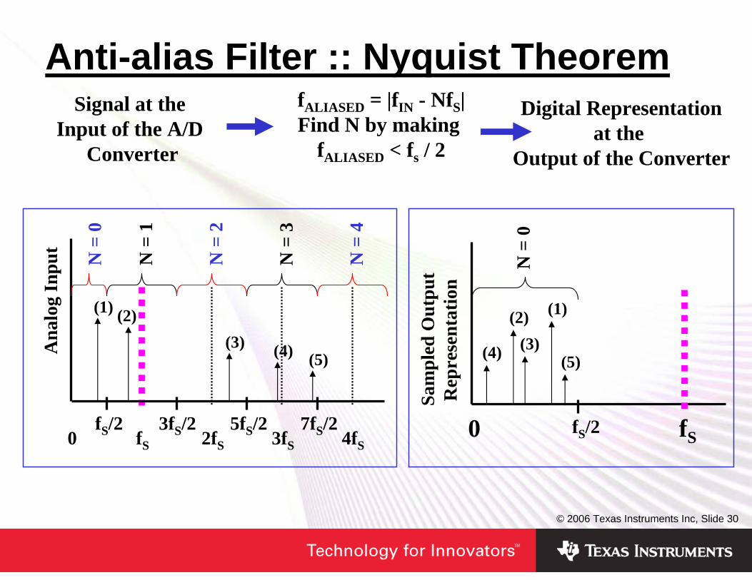
0 fS 2fS 3fS 4fSfS/2 3fS/2 5fS/2 7fS/2
N =
1
N =
0
N =
2
N =
3
N =
4
(1) (2)(3) (4) (5)A
nalo
g In
put
0 fSfS/2
N =
0
(1)(2)(3)(4) (5)
Sam
pled
Out
put
Rep
rese
ntat
ion
Signal at the Input of the A/D
Converter
fALIASED = |fIN - NfS|Find N by making
fALIASED < fs / 2
Digital Representationat the
Output of the Converter
Anti-alias Filter :: Nyquist Theorem
© 2006 Texas Instruments Inc, Slide 31
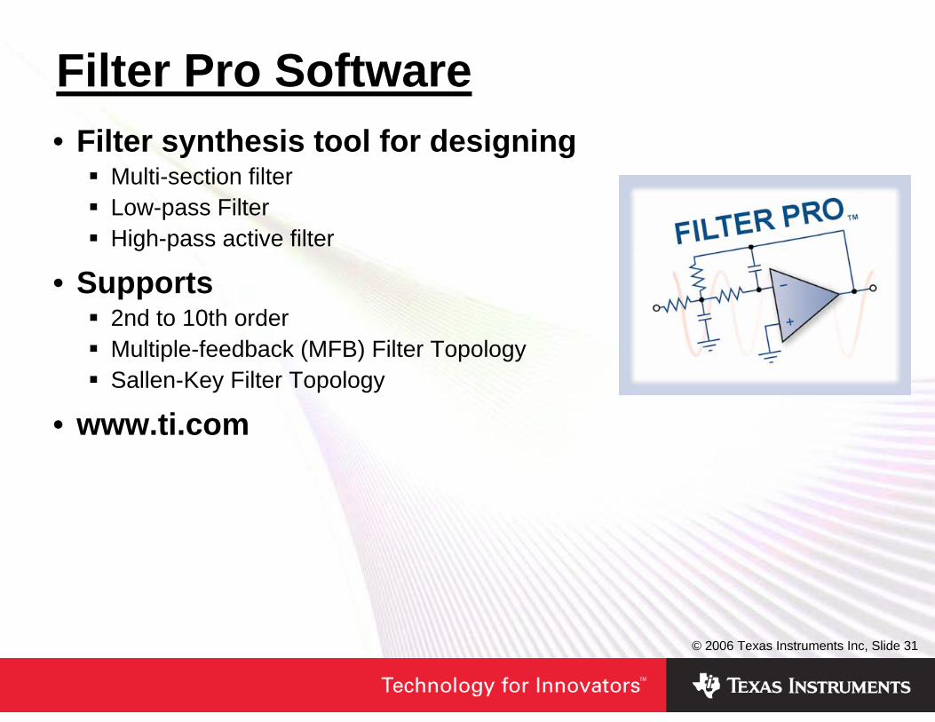
Filter Pro Software• Filter synthesis tool for designing
Multi-section filterLow-pass FilterHigh-pass active filter
• Supports 2nd to 10th orderMultiple-feedback (MFB) Filter TopologySallen-Key Filter Topology
• www.ti.com
© 2006 Texas Instruments Inc, Slide 32
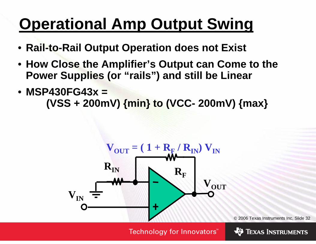
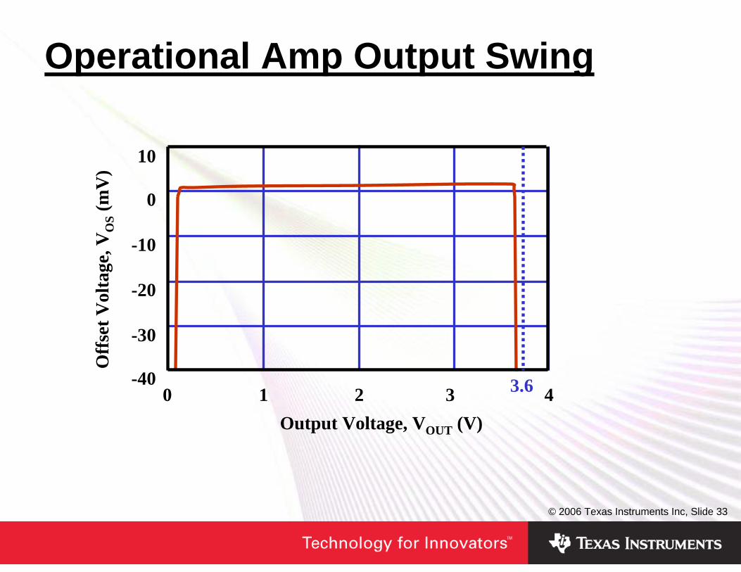
Operational Amp Output Swing• Rail-to-Rail Output Operation does not Exist• How Close the Amplifier’s Output can Come to the
Power Supplies (or “rails”) and still be Linear• MSP430FG43x =
(VSS + 200mV) {min} to (VCC- 200mV) {max}
VOUT = ( 1 + RF / RIN) VIN
VOUTVIN
RFRIN
© 2006 Texas Instruments Inc, Slide 33
Operational Amp Output Swing
30 1 2 4-40
-30
-20
-10
0
10
Output Voltage, VOUT (V)
Off
set V
olta
ge, V
OS
(mV
)
3.6
© 2006 Texas Instruments Inc, Slide 34
MSP430FG43x
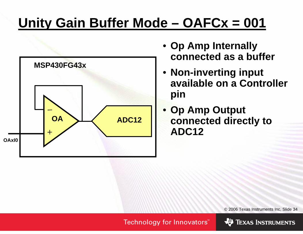
Unity Gain Buffer Mode – OAFCx = 001
+
−OA ADC12
OAxI0
• Op Amp Internally connected as a buffer
• Non-inverting input available on a Controller pin
• Op Amp Output connected directly to ADC12
© 2006 Texas Instruments Inc, Slide 35
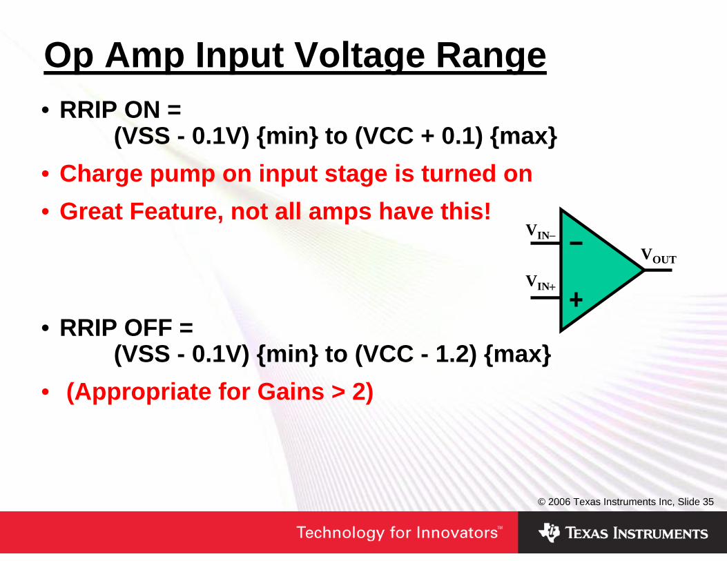
Op Amp Input Voltage Range• RRIP ON =
(VSS - 0.1V) {min} to (VCC + 0.1) {max}• Charge pump on input stage is turned on• Great Feature, not all amps have this!
• RRIP OFF = (VSS - 0.1V) {min} to (VCC - 1.2) {max}
• (Appropriate for Gains > 2)
VIN−
VIN+
VOUT
© 2006 Texas Instruments Inc, Slide 36
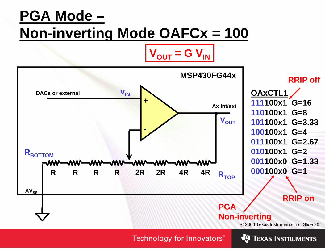
OAxCTL1111100x1 G=16110100x1 G=8101100x1 G=3.33100100x1 G=4011100x1 G=2.67010100x1 G=2001100x0 G=1.33000100x0 G=1
PGA Mode –Non-inverting Mode OAFCx = 100
DACs or external
MSP430FG44x
4R4R2R2RRRRR RTOP
RBOTTOM
+
-
AVSS
Ax int/ext
PGA Non-inverting
RRIP on
RRIP off
VOUT
VIN
VOUT = G VIN

© 2006 Texas Instruments Inc, Slide 37
OAxCTL1111110x1 G=-15110110x1 G=-7101110x1 G=-4.33100110x1 G=-3011110x1 G=2.67010110x1 G=-1.67001110x1 G=-1000110x0 G=-0.33
PGA Mode –Inverting Mode OAFCx = 110
DACsor external
MSP430FG44x
4R4R2R2RRRRR RTOPRBOTTOM
+
-
Ax int/ext
PGA Inverting
VREF
VOUT
VIN
VOUT = G VIN + VREF(1 – G)
RRIP on
RRIP off
© 2006 Texas Instruments Inc, Slide 38
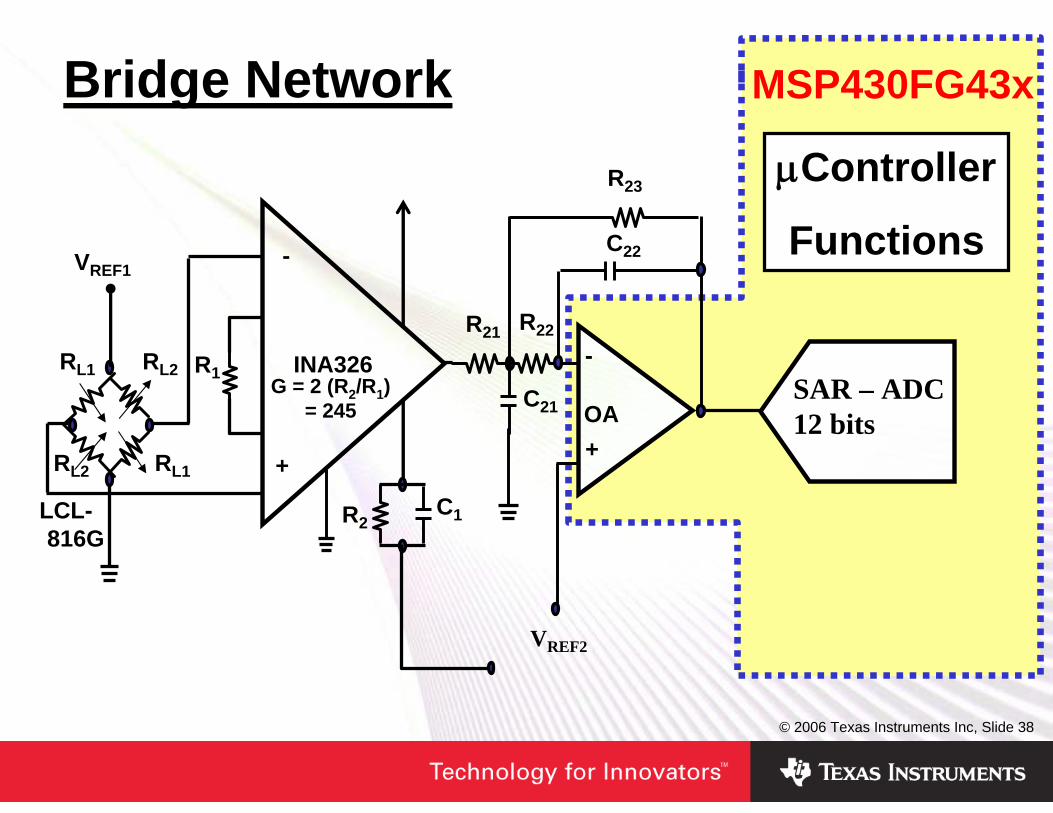
LCL-816G
RL1 RL2
RL1RL2
VREF1
R1
C22
R23
+
-
OA
R21 R22
C21
+
-
INA326
R2C1
G = 2 (R2/R1) = 245
VREF2
Bridge Network
SAR – ADC12 bits
MSP430FG43x
μController
Functions
© 2006 Texas Instruments Inc, Slide 39
Summary• 12-bit SAR Converter – ADC12
12-bit Resolution and AccuracyExcellent Dynamic RangeFor more Resolution – Discrete Options
• Operational Amplifier – OAStandard Single Supply CMOS Op AmpRail-to-rail InputRail-to-rail OutputSix Configurations or ModesFor more Accuracy – Discrete OptionsFor more Complexity – Discrete Options
• MSP430 Analog Options – Very Useful!

IMPORTANT NOTICE
Texas Instruments Incorporated and its subsidiaries (TI) reserve the right to make corrections, modifications, enhancements,improvements, and other changes to its products and services at any time and to discontinue any product or service without notice.Customers should obtain the latest relevant information before placing orders and should verify that such information is current andcomplete. All products are sold subject to TI’s terms and conditions of sale supplied at the time of order acknowledgment.
TI warrants performance of its hardware products to the specifications applicable at the time of sale in accordance with TI’sstandard warranty. Testing and other quality control techniques are used to the extent TI deems necessary to support thiswarranty. Except where mandated by government requirements, testing of all parameters of each product is not necessarilyperformed.
TI assumes no liability for applications assistance or customer product design. Customers are responsible for their products andapplications using TI components. To minimize the risks associated with customer products and applications, customers shouldprovide adequate design and operating safeguards.
TI does not warrant or represent that any license, either express or implied, is granted under any TI patent right, copyright, maskwork right, or other TI intellectual property right relating to any combination, machine, or process in which TI products or servicesare used. Information published by TI regarding third-party products or services does not constitute a license from TI to use suchproducts or services or a warranty or endorsement thereof. Use of such information may require a license from a third party underthe patents or other intellectual property of the third party, or a license from TI under the patents or other intellectual property of TI.
Reproduction of information in TI data books or data sheets is permissible only if reproduction is without alteration and isaccompanied by all associated warranties, conditions, limitations, and notices. Reproduction of this information with alteration is anunfair and deceptive business practice. TI is not responsible or liable for such altered documentation.
Resale of TI products or services with statements different from or beyond the parameters stated by TI for that product or servicevoids all express and any implied warranties for the associated TI product or service and is an unfair and deceptive businesspractice. TI is not responsible or liable for any such statements.
TI products are not authorized for use in safety-critical applications (such as life support) where a failure of the TI product wouldreasonably be expected to cause severe personal injury or death, unless officers of the parties have executed an agreementspecifically governing such use. Buyers represent that they have all necessary expertise in the safety and regulatory ramificationsof their applications, and acknowledge and agree that they are solely responsible for all legal, regulatory and safety-relatedrequirements concerning their products and any use of TI products in such safety-critical applications, notwithstanding anyapplications-related information or support that may be provided by TI. Further, Buyers must fully indemnify TI and itsrepresentatives against any damages arising out of the use of TI products in such safety-critical applications.
TI products are neither designed nor intended for use in military/aerospace applications or environments unless the TI products arespecifically designated by TI as military-grade or "enhanced plastic." Only products designated by TI as military-grade meet militaryspecifications. Buyers acknowledge and agree that any such use of TI products which TI has not designated as military-grade issolely at the Buyer's risk, and that they are solely responsible for compliance with all legal and regulatory requirements inconnection with such use.
TI products are neither designed nor intended for use in automotive applications or environments unless the specific TI productsare designated by TI as compliant with ISO/TS 16949 requirements. Buyers acknowledge and agree that, if they use anynon-designated products in automotive applications, TI will not be responsible for any failure to meet such requirements.
Following are URLs where you can obtain information on other Texas Instruments products and application solutions:
Products Applications
Amplifiers amplifier.ti.com Audio www.ti.com/audio
Data Converters dataconverter.ti.com Automotive www.ti.com/automotive
DSP dsp.ti.com Broadband www.ti.com/broadband
Interface interface.ti.com Digital Control www.ti.com/digitalcontrol
Logic logic.ti.com Military www.ti.com/military
Power Mgmt power.ti.com Optical Networking www.ti.com/opticalnetwork
Microcontrollers microcontroller.ti.com Security www.ti.com/security
RFID www.ti-rfid.com Telephony www.ti.com/telephony
Low Power www.ti.com/lpw Video & Imaging www.ti.com/videoWireless
Wireless www.ti.com/wireless
Mailing Address: Texas Instruments, Post Office Box 655303, Dallas, Texas 75265Copyright © 2007, Texas Instruments Incorporated