Embed Size (px)
Citation preview

Working T13Draft 1153D
Revision 1819 August 1998
Information Technology -AT Attachmentwith Packet Interface Extension(ATA/ATAPI-4)
This is an internal working document of T13, a Technical Committee of Accredited Standards CommitteeNCITS. As such, this is not a completed standard and has not been approved. The contents may bemodified by the T13 Technical Committee. This document is made available for review and comment only.
Permission is granted to members of NCITS, its technical committees, and their associated task groups toreproduce this document for the purposes of NCITS standardization activities without further permission,provided this notice is included. All other rights are reserved. Any commercial or for-profit replication orrepublication is prohibited.
ASC T13 Technical Editor:Peter T. McLeanMaxtor Corporation2190 Miller DriveLongmont, CO 80501-6744USA
Tel: 303-678-2149Fax: 303-682-4811Email: [email protected]
Reference numberANSI X3.*** - 199x
Printed August, 20, 1998 9:50AM

T13/1153D revision 18
Other Points of Contact:
T13 Chair T13 Vice-ChairGene Milligan Pete McLeanSeagate Technology Maxtor CorporationOKM 251 2190 Miller Drive10323 West Reno (West Dock) Longmont, CO 80501P.O. Box 12313 Tel: 303-678-2149Oklahoma City, OK 73157-2313 Fax: 303-682-4811Tel: 405-324-3070Fax: 405-324-3794
NCITS SecretariatAdministrator Standards Processing1250 Eye Street, NW Suite 200Washington, DC 20005Tel: 202-737-8888Fax: 202-638-4922Email: [email protected]
T13 ReflectorInternet address for subscription to the T13 reflector: [email protected] email to above account and include in BODY of text, on a line by itself the following:
"subscribe T13 [your email address]"Internet address for distribution via T13 reflector: [email protected]
T13 Anonymous FTP Sitefission.dt.wdc.comT13 directory is: "/ t13 "
T13 mailingsGlobal Engineering15 Inverness Way EastEnglewood, CO 80112-5704Tel: 303-792-2181 or 800-854-7179Fax: 303-792-2192

T13/1153D revision 18
DOCUMENT STATUS
Revision 0 - 5 February 1996
Document created from ATA3-r6 (X3T10/2008Dr6) with new frontmatter and the content of AT AttachmentPacket Interface (X3T10/1120Dr2) added.
Revision 1 - 18 March 1996
Per 2/21-23/96 working group meeting:• Changed document name• Removed term ATA from text of document• Added output table to each command, moved table 6, and equivalent ATAPI table to Annex E• Filled in na (not applicable) in command input and output tables• Added PACKET bit descriptions in register descriptions clause 6.• Added new clause 7.1 and rearranged clause 7.• Made other text changes requested during page by page review.
Revision 2 - 5 April 1996
Per 3/27-29/96 working group meeting:• Eliminated phrase “not used”/”not to be used”.• Added “signature” the definitions and Protocol clause.• Added SFF8020 reference and in bibliography.• Swapped clauses 6 and 7.• Reworded new clause 7, Register definitions to contains only material common to all
commands.• Added subclauses to clause 8, Commands.• Made text changes requested during page-by-page review.
Revision 3 - 3 May 1996
Per 4/24-25/96 working group meeting:• Modified PACKET protocol flowcharts as requested• Added proposal D96102R2, Pins A-D on 44-pin connector• Made text changes requested during review• Added ATA3 letter ballot comment resolution
Revision 4 - 10 June 1996
Added revisions per page-by-page review at 5/22-24/96 working group meeting
Revision 5 - 28 June 1996
Added proposals:• D96125R5 Vendor specific and optional commands• D96137R0 Protected area proposal• D96131R1 SMART change proposal
Added register transfer timing.Added revisions per page-by-page review at 6/19-21/96 working group meeting.
T13/1153D revision 18
Revision 6 - 6 September 1996
Added editorial changes from the ATA-3 ANSI pre-edit.Added proposal D96106r1, FLUSH CACHE, as modified at the 7/31/96 working group meeting.Added ATA/ATAPI-4 revision 6 to revisions list in IDENTIFY DEVICE response.IORDY description in clause 5.2.11 changed to allow only tristate drivers.Added description of invalid register address in Interface register definitions and descriptions clause.Made “a” power management feature mandatory in the Power Management feature set.Moved timing conventions to Conventions clause.
Revision 7 - 3 October 1996
Per September 25-26 working group meeting:Added Feature Status Reporting, D96103R2 with revisions.Added PACKET feature set queuing from D96104R8.Added Removing Redundant Information proposal, D96114R1, except for timing diagram changes.Added unitized connectors, D96126R1 and D96149R0.Added modified reset protocol, D96142R6.Added changes per page-by-page review.
Revision 8 - 3 December 1996
Per October 23-24 and November 13-15 working group meetings:Added READ/WRITE DMA O/Q commands (D96104R9).Added new timing diagrams (D96114R2).Added reset changes (D96157R0).Added changes per page by page reviews.
Revision 9 - 10 February 1997
Removed Removable Media feature setAdded register access restrictions proposal (D97102R0)Added SET MAX ADDRESS addition (D97106R1)Added enhanced security erase proposal (D96156R2)Added Ultra DMA proposal (D96153R3)Made changes requested by page by page review through clause 8.9.
Revision 10 - 7 March 1997
Made changes requested by page-by-page review at February meeting.Modified protocol flowcharts in clause 9.
Revision 11 - 1 April 1997
Added Ultra DMA changes from D96153R4.Modified protocol flow charts as requested at March meeting.Made changes per change bar review at March meeting.
Revision 12 - 2 May 1997
Added CFA feature set per D97116R2.Modified protocol flowcharts per April meeting review.Made changes per change bar review at April meeting.

T13/1153D revision 18
Revision 13 - 30 May 1997
Added Advanced Power Management per D97126R2.Modified clauses 5.2.9, 6.6, and 6.7 to eliminate overlap/queue race.Modified protocol flowcharts per May meeting.Made changes per change bar review at May meeting.
Revision 14 - 26 June 1997
Made WRITE VERIFY command obsolete.Added Removable Media Status Notification proposal per D97120R2.Added 80-conductor assembly proposal per D97121R1.Added new SET MAX/NATIVE MAX description per D97119R3.Modified signature and persistence clause per D97139R0.Modified protocol flowcharts per June meeting.Made changes per change bar review at June meeting.
Revision 15 - 1 August 1997
Added Cleanup proposal per D97139R1.Modified Annex B per D97138R3.Modified Annex C per D97128R2.Made changes per change bar review at July meeting.
Revision 16 - 25 August 1997
Added C/H/S and LBA calculation rules per D97145R3.Made changes per change bar review at August meeting.
Revision 17 - 30 October 1997
Added changes per resolution of letter ballot comments, D97152R1.
Revision 18 - 19 August 1998
Added editorial changes per D98121r1.

T13/1153D revision 18
Page left intentionally blank

T13/1153D revision 18
ANSI®
X3.****-199x
American National Standardfor Information Systems
AT Attachmentwith Packet Interface Extension (ATA/ATAPI-4)
SecretariatInformation Technology Industry Council
Approved mm dd yy
American National Standards Institute, Inc.
Abstract
This standard specifies the AT Attachment Interface between host systems and storage devices. It providesa common attachment interface for systems manufacturers, system integrators, software suppliers, andsuppliers of intelligent storage devices. It includes the Packet Command feature set implemented bydevices commonly known as ATAPI devices.
This standard maintains a high degree of compatibility with the AT Attachment-3 Interface (ATA-3), X3.298-1997, and while providing additional functions, is not intended to require changes to presently installeddevices or existing software.

T13/1153D revision 18
AmericanNationalStandard
Approval of an American National Standard requires verification by ANSI that therequirements for due process, consensus, and other criteria for approval havebeen met by the standards developer. Consensus is established when, in thejudgment of the ANSI Board of Standards Review, substantial agreement hasbeen reached by directly and materially affected interests. Substantial agreementmeans much more than a simple majority, but not necessarily unanimity.Consensus requires that all views and objections be considered, and that effort bemade towards their resolution.
The use of American National Standards is completely voluntary; their existencedoes not in any respect preclude anyone, whether he has approved the standardsor not, from manufacturing, marketing, purchasing, or using products, processes,or procedures not conforming to the standards.
The American National Standards Institute does not develop standards and will inno circumstances give interpretation on any American National Standard.Moreover, no person shall have the right or authority to issue an interpretation ofan American National Standard in the name of the American National StandardsInstitute. Requests for interpretations should be addressed to the secretariat orsponsor whose name appears on the title page of this standard.
CAUTION NOTICE: This American National Standard may be revised orwithdrawn at any time. The procedures of the American National StandardsInstitute require that action be taken periodically to reaffirm, revise, or withdrawthis standard. Purchasers of American National Standards may receive currentinformation on all standards by calling or writing the American National StandardsInstitute.
CAUTION: The developers of this standard have requested that holders of patents that may berequired for the implementation of the standard, disclose such patents to the publisher. However,neither the developers nor the publisher have undertaken a patent search in order to identifywhich, if any, patents may apply to this standard.
As of the date of publication of this standard and following calls for the identification of patents thatmay be required for the implementation of the standard, notice of one or more such claims hasbeen received.
By publication of this standard, no position is taken with respect to the validity of this claim or ofany rights in connection therewith. The patent holders have, however, filed a statement ofwillingness to grant a license under these rights on reasonable and nondiscriminatory terms andconditions to applicants desiring to obtain such a license. Details may be obtained from thepublisher.
No further patent search is conducted by the developer or the publisher in respect to any standardit processes. No representation is made or implied that licenses are not required to avoidinfringement in the use of this standard.
Published byAmerican National Standards Institute11 West 42nd Street, New York, New York 10036
Copyright 199n by American National Standards InstituteAll rights reserved.

T13/1153D revision 18
Page i
Contents Page
Foreword .............................................................................................................................................vIntroduction .........................................................................................................................................ix1 Scope...............................................................................................................................................12 Normative references .......................................................................................................................2
2.1 Approved references...............................................................................................................22.2 References under development ..............................................................................................22.3 Other references.....................................................................................................................2
3 Definitions, abbreviations, and conventions ......................................................................................33.1 Definitions and abbreviations ..................................................................................................33.2 Conventions............................................................................................................................5
4 Interface physical and electrical requirements ...................................................................................94.1 Cable configuration .................................................................................................................94.2 I/O cable .................................................................................................................................104.3 Electrical characteristics .........................................................................................................10
5 Interface signal assignments and descriptions ..................................................................................135.1 Signal summary ......................................................................................................................135.2 Signal descriptions..................................................................................................................14
6 General operational requirements .....................................................................................................196.1 Command delivery ..................................................................................................................196.2 Register delivered data transfer command sector addressing .................................................196.3 General feature set .................................................................................................................216.4 Ultra DMA feature set .............................................................................................................226.5 PACKET Command feature set ..............................................................................................246.6 Overlapped feature set ...........................................................................................................256.7 Queued feature set .................................................................................................................266.8 Power Management feature set ..............................................................................................276.9 Advanced Power Management feature set ..............................................................................296.10 Security Mode feature set .....................................................................................................306.11 Self-monitoring, analysis, and reporting technology feature set .............................................346.12 Host Protected Area feature set ............................................................................................356.13 CFA feature Set ....................................................................................................................366.14 Removable Media Status Notification and Removable Media feature sets ............................37
7 Interface register definitions and descriptions ...................................................................................397.1 Device addressing considerations ...........................................................................................397.2 I/O register descriptions ..........................................................................................................397.3 Alternate Status register..........................................................................................................417.4 Command register ..................................................................................................................417.5 Cylinder High register .............................................................................................................427.6 Cylinder Low register ..............................................................................................................427.7 Data register ...........................................................................................................................437.8 Data port.................................................................................................................................437.9 Device Control register ...........................................................................................................447.10 Device/Head register ............................................................................................................457.11 Error register.........................................................................................................................467.12 Features register...................................................................................................................467.13 Sector Count register ............................................................................................................477.14 Sector Number register .........................................................................................................477.15 Status register.......................................................................................................................48
8 Command descriptions .....................................................................................................................528.1 CFA ERASE SECTORS .........................................................................................................548.2 CFA REQUEST EXTENDED ERROR CODE .........................................................................56

T13/1153D revision 18
Page ii
8.3 CFA TRANSLATE SECTOR...................................................................................................598.4 CFA WRITE MULTIPLE WITHOUT ERASE ...........................................................................618.5 CFA WRITE SECTORS WITHOUT ERASE ...........................................................................638.6 CHECK POWER MODE .........................................................................................................658.7 DEVICE RESET .....................................................................................................................678.8 DOWNLOAD MICROCODE ...................................................................................................698.9 EXECUTE DEVICE DIAGNOSTIC..........................................................................................718.10 FLUSH CACHE ....................................................................................................................738.11 GET MEDIA STATUS...........................................................................................................758.12 IDENTIFY DEVICE ...............................................................................................................778.13 IDENTIFY PACKET DEVICE ................................................................................................958.14 IDLE .....................................................................................................................................1058.15 IDLE IMMEDIATE.................................................................................................................1088.16 INITIALIZE DEVICE PARAMETERS.....................................................................................1108.17 MEDIA EJECT......................................................................................................................1138.18 MEDIA LOCK .......................................................................................................................1158.19 MEDIA UNLOCK ..................................................................................................................1178.20 NOP .....................................................................................................................................1198.21 PACKET ...............................................................................................................................1218.22 READ BUFFER ....................................................................................................................1278.23 READ DMA...........................................................................................................................1298.24 READ DMA QUEUED...........................................................................................................1328.25 READ MULTIPLE .................................................................................................................1368.26 READ NATIVE MAX ADDRESS ...........................................................................................1398.27 READ SECTOR(S) ...............................................................................................................1418.28 READ VERIFY SECTOR(S) .................................................................................................1448.29 SECURITY DISABLE PASSWORD ......................................................................................1478.30 SECURITY ERASE PREPARE.............................................................................................1498.31 SECURITY ERASE UNIT .....................................................................................................1518.32 SECURITY FREEZE LOCK ..................................................................................................1548.33 SECURITY SET PASSWORD ..............................................................................................1568.34 SECURITY UNLOCK............................................................................................................1598.35 SEEK....................................................................................................................................1618.36 SERVICE..............................................................................................................................1648.37 SET FEATURES...................................................................................................................1658.38 SET MAX ADDRESS............................................................................................................1708.39 SET MULTIPLE MODE.........................................................................................................1738.40 SLEEP..................................................................................................................................1758.41 SMART.................................................................................................................................1778.42 STANDBY.............................................................................................................................1958.43 STANDBY IMMEDIATE ........................................................................................................1978.44 WRITE BUFFER...................................................................................................................1998.45 WRITE DMA.........................................................................................................................2018.46 WRITE DMA QUEUED .........................................................................................................2048.47 WRITE MULTIPLE ...............................................................................................................2088.48 WRITE SECTOR(S) .............................................................................................................211
9 Protocol ............................................................................................................................................2149.1 Signature and persistence.......................................................................................................2149.2 Power on and hardware resets................................................................................................2159.3 Software reset.........................................................................................................................2199.4 DEVICE RESET protocol ........................................................................................................2239.5 EXECUTE DEVICE DIAGNOSTIC protocol ............................................................................2249.6 Device selection protocol ........................................................................................................2279.7 PIO data in command protocol................................................................................................2289.8 PIO data out command protocol .............................................................................................2319.9 Non-data command protocol ...................................................................................................235

T13/1153D revision 18
Page iii
9.10 DMA command protocol .......................................................................................................2379.11 PACKET command protocol .................................................................................................2399.12 READ/WRITE DMA QUEUED command protocol ................................................................2539.13 Ultra DMA data in commands ...............................................................................................2579.14 Ultra DMA data out commands .............................................................................................2599.15 Ultra DMA CRC rules ............................................................................................................2629.16 Single device configurations .................................................................................................265
10 Timing ............................................................................................................................................26610.1 Deskewing ............................................................................................................................26610.2 Transfer timing......................................................................................................................266
Tables Page
1 Byte order........................................................................................................................................82 DC characteristics............................................................................................................................103 AC characteristics............................................................................................................................104 Driver types and required termination ..............................................................................................115 Typical series termination for Ultra DMA ...........................................................................................126 Interface signal name assignments ..................................................................................................137 Security mode command actions .....................................................................................................338 Extended error codes........................................................................................................................579 CFA TRANSLATE SECTOR information ..........................................................................................6010 Diagnostic codes ...........................................................................................................................7211 Identify device information .............................................................................................................7912 Minor revision number ...................................................................................................................9013 Identify packet device information .................................................................................................9714 Automatic standby timer periods ....................................................................................................10515 Security password content .............................................................................................................14816 SECURITY ERASE UNIT password................................................................................................15317 SECURITY SET PASSWORD data content...................................................................................15718 Identifier and security level bit interaction ......................................................................................15819 SET FEATURES register definitions ..............................................................................................16720 Transfer/mode values ....................................................................................................................16821 Advanced power management levels .............................................................................................16822 SMART Feature register values ......................................................................................................17723 Device SMART data structure........................................................................................................18924 Off-line data collection status byte values ......................................................................................18925 BSY and DRDY timing for power on and hardware resets ..............................................................21926 BSY and DRDY timing for software reset .......................................................................................22327 BSY and DRDY timing for diagnostic command .............................................................................22628 Equations for parallel generation of a CRC polynomial ...................................................................26329 Register transfer to/from device .....................................................................................................26830 PIO data transfer to/from device ....................................................................................................27031 Multiword DMA data transfer..........................................................................................................27232 Ultra DMA data burst timing requirements ......................................................................................274

T13/1153D revision 18
Page iv
Figures Page
1 Interface cabling diagram ................................................................................................................92 Ultra DMA termination with pull-up or pull-down ................................................................................123 PDIAG- example using an 80-conductor cable assembly ..................................................................164 Cable select example ......................................................................................................................175 Alternate cable select example .........................................................................................................186 Power management modes .............................................................................................................297 Security mode flow ..........................................................................................................................328 BSY and DRDY timing for power on and hardware resets ................................................................2189 BSY and DRDY timing for software reset .........................................................................................22210 BSY and DRDY timing for diagnostic command .............................................................................22611 Device selection protocol ................................................................................................................22712 PIO data in command protocol .......................................................................................................22813 PIO data out command protocol .....................................................................................................23114 Non-data command protocol ...........................................................................................................23615 DMA command protocol .................................................................................................................23716 PACKET non-data and PIO data command protocol .......................................................................23917 PACKET DMA command protocol ..................................................................................................24618 READ/WRITE DMA QUEUED command protocol .........................................................................25319 Example parallel CRC generator ....................................................................................................26320 Register transfer to/from device .....................................................................................................26721 PIO data transfer to/from device ....................................................................................................26922 Multiword DMA data transfers ........................................................................................................27123 Initiating an Ultra DMA data in burst................................................................................................27324 Sustained Ultra DMA data in burst ..................................................................................................27625 Host pausing an Ultra DMA data in burst.........................................................................................27726 Device terminating an Ultra DMA data in burst ...............................................................................27827 Host terminating an Ultra DMA data in burst ...................................................................................27928 Initiating an Ultra DMA data out burst .............................................................................................28029 Sustained Ultra DMA data out burst ................................................................................................28130 Device pausing an Ultra DMA data out burst ...................................................................................28231 Host terminating an Ultra DMA data out burst .................................................................................28332 Device terminating an Ultra DMA data out burst .............................................................................284
Annexes Page
A Connectors.......................................................................................................................................285B Identify device data for devices with more than 1024 logical cylinders .............................................295C Signal integrity .................................................................................................................................298D Bibliography .....................................................................................................................................323E ATA command set summary ............................................................................................................324F Command packet format example ....................................................................................................329
T13/1153D revision 18
Page v
Foreword(This foreward is not part of American National Standard X3.***-199*.)
This AT Attachment with Packet Interface Extension (ATA/ATAPI-4) standard is designed to maintain ahigh degree of compatibility with the AT Attachment-3 Interface (ATA-3) standard and the packet commandfeature set implemented by devices commonly known as ATAPI devices while providing the advantages ofadditional features and functions.
This standard was developed by the ATA ad hoc working group of Accredited Standards Committee NCITSduring 1995-97. The standards approval process started in 1997. This document includes annexes that areinformative and are not considered part of the standard.
Requests for interpretation, suggestions for improvement and addenda, or defect reports are welcome. Theyshould be sent to the NCITS Secretariat, Information Technology Industry Council, 1250 Eye Street, NW,Suite 200, Washington, DC 20005-3922.
This standard was processed and approved for submittal to ANSI by Accredited Standards Committee onInformation Processing Systems, NCITS. Committee approval of the standard does not necessarily implythat all committee members voted for approval. At the time it approved this standard, the NCITS Committeehad the following members:
James D. Converse, Chair
Donald C. Loughry, Vice-Chair
Joanne M. Flanagan, Secretary
Organization Represented .......................................................................Name of RepresentativeAmerican Nuclear Society .......................................................................Geraldine C. Main
Sally Hartzell (Alt.)AMP, Inc .................................................................................................Edward Kelly
Charles Brill (Alt.)Apple Computer ......................................................................................Karen HigginbottomAssociation of the Institute for Certification of Professionals (AICCP) ......Kennath ZemrowskiAT&T/NCR ..............................................................................................Thomas W. Kern
Thomas F. Frost (Alt.)Boeing Company .....................................................................................Catherine Howells
Andrea Vanosdoll (Alt.)Bull HN Information Systems, Inc. ...........................................................William GeorgeCompaq Computer Corporation ...............................................................James BarnesDigital Equipment Corporation .................................................................Delbert Shoemaker
Kevin Lewis (Alt.)Eastman Kodak .......................................................................................James D. Converse
Michael Nier (Alt.)GUIDE International ................................................................................Frank Kirshenbaum
Harold Kuneke (Alt.)Hewlett-Packard ......................................................................................Donald C. LoughryHitachi America, Ltd. ...............................................................................John Neumann
Kei Yamashita (Alt.)Hughes Aircraft Company........................................................................Harold L. ZebrackIBM Corporation ......................................................................................Joel Urman
Mary Anne Lawler (Alt.)National Communication Systems ...........................................................Dennis BodsonNational Institute of Standards and Technology .......................................Robert E. Roundtree
Michael Hogan (Alt.)Northern Telecom, Inc. ............................................................................Mel Woinsky
Subhash Patel (Alt.)Neville & Associates ................................................................................Carlton Neville

T13/1153D revision 18
Page vi
Recognition Technology Users Association..............................................Herbert P. SchantzG. Edwin Hale (Alt.)
Share, Inc................................................................................................Gary AinsworthDavid Thewlis (Alt.)
Sony Corporation.....................................................................................Michael DeeseStorage Technology Corporation .............................................................Joseph S. Zajaczkowski
Samuel D. Cheatham (Alt.)Sun Microsystems ...................................................................................Scott Jameson
Gary Robinson (Alt.)3M Company ...........................................................................................Eddie T. Morioka
Paul D. Jahnke (Alt.)Unisys Corporation ..................................................................................John L. Hill
Stephen P. Oksala (Alt.)U.S. Department of Defense....................................................................William C. Rinehuls
C. J. Pasquariello (Alt.)U.S. Department of Energy......................................................................Alton Cox
Lawrence A. Wasson (Alt.)U.S. General Services Administration ......................................................Douglas Arai
Larry L. Jackson (Alt.)Wintergreen Information Services ...........................................................Joun WheelerXerox Corporation ...................................................................................Dwight McBain
Roy Peirce (Alt.)
Subcommittee T13 on ATA Interfaces, that reviewed this standard, had the following members:
Gene Milligan, Chairman
Pete McLean, Vice-Chairman
Larry Lamers, Secretary
I. Dal Allan Paul Raikunen Richard Harcourt (Alt.)Charles Brill Yogi Schaffner Pat LaVarre (Alt.)Darrin Bulik J. R. Sims LeRoy Leach (Alt.)Ben Chang Victor Siu Raymond Liang (Alt.)Dan Colegrove Ron Stephens John Masiewicz (Alt.)Greg Elkins Curtis Stevens Christopher Mayne (Alt.)Mark Evans Tokuyuki Totani James McGrath (Alt.)Lance Flake Anthony Yang Patrick Mercer (Alt.)Tony Goodfellow Carl Bonke (Alt.) Marc Noblitt (Alt.)Tom Hanan Joe Chen (Alt.) Ron Roberts (Alt.)Richard Kalish Mike Christensen (Alt.) Yasuyuki Suemori (Alt.)Kenichi Kojima David Evans (Alt.) Don Vohar (Alt.)Hale Landis Stephen Finch (Alt.) Devon Worrell (Alt.)Robert Liu Robert Griffith (Alt.)
ATA/ATAPI ad hoc Working Group, that developed this standard, had the following additional participants:
Evgeny Berzon Shinichi Kobayashi Norihiko OshitaGeorge Blattner Eric Kvamme Steven PengJeff Cousins Tony Kwan Duncan PenmanLang Dennis Bill Mable Jerry SaltzmanFarbod Falakfars John Mallory Andrew ShuRobin Freeze Kent Manabe Trent ThomasGregg Goldman John Mangan Irv TjomslandYoshihito Higashitsutsumi Terry Miller Ron WerbowSon Ho Masa Morizumi Mike WinchellPaul Jackson Kazou Nakashima Jauher ZaidiEarle Jennings Jay Neer
T13/1153D revision 18
Page vii
Introduction
This standard encompasses the following:
Clause 1 describes the scope.
Clause 2 provides normative references.
Clause 3 provides definitions, abbreviations, and conventions used within this document.
Clause 4 contains the electrical and mechanical characteristics; covering the interface cablingrequirements of the interface and DC cables and connectors.
Clause 5 contains the signal descriptions of the AT Attachment Interface.
Clause 6 describes the general operating requirements of the AT Attachment Interface.
Clause 7 contains descriptions of the registers of the AT Attachment Interface.
Clause 8 contains descriptions of the commands of the AT Attachment Interface.
Clause 9 contains the protocol of the AT Attachment Interface.
Clause 10 contains the interface timing diagrams.

T13/1153D revision 18
Page viii
(This page intentionally blank)

T13/1153D revision 18
Page 1
AMERICAN NATIONAL STANDARD X3.****-199n
American National Standardfor Information Systems
Information Technology AT Attachment with Packet Interface Extension (ATA/ATAPI-4)
1 Scope
This standard specifies the AT Attachment Interface between host systems and storage devices. It providesa common attachment interface for systems manufacturers, system integrators, software suppliers, andsuppliers of intelligent storage devices.
The application environment for the AT Attachment Interface is any host system that has storage devicescontained within the processor enclosure.
This standard defines the connectors and cables for physical interconnection between host and storagedevice, as well as, the electrical and logical characteristics of the interconnecting signals. It also defines theoperational registers within the storage device, and the commands and protocols for the operation of thestorage device.
This standard maintains a high degree of compatibility with the AT Attachment-3 Interface standard (ATA-3),X3.298-1997, and while providing additional functions, is not intended to require changes to presentlyinstalled devices or existing software.

T13/1153D revision 18
Page 2
2 Normative references
The following standards contain provisions that, through reference in the text, constitute provisions of thisstandard. At the time of publication, the editions indicated were valid. All standards are subject to revision,and parties to agreements based on this standard are encouraged to investigate the possibility of applyingthe most recent editions of the standards listed below.
Copies of the following documents can be obtained from ANSI: Approved ANSI standards, approved anddraft international and regional standards (ISO, IEC, CEN/CENELEC, ITUT), and approved and draft foreignstandards (including BSI, JIS, and DIN). For further information, contact ANSI Customer ServiceDepartment at 212-642-4900 (phone), 212-302-1286 (fax) or via the World Wide Web athttp://www.ansi.org.
Additional availability contact information is provided below as needed.
2.1 Approved references
The following approved ANSI standards, approved international and regional standards (ISO, IEC,CEN/CENELEC, ITUT), may be obtained from the international and regional organizations who controlthem.
SCSI-3 Primary Commands (SPC) [NCITS 301:1997] (PACKET command feature set device types)SCSI-3 Multimedia Commands (MMC) [NCITS 304:1997] (PACKET command feature set sense codes)
To obtain copies of these documents, contact Global Engineering or NCITS.
2.2 References under development
At the time of publication, the following referenced standards were still under development. For informationon the current status of the document, or regarding availability, contact the relevant standards body or otherorganization as indicated.
Multimedia Commands - 2 (MMC-2) [T10/1228-D] (PACKET command feature set commands)
For more information on the current status of the above documents, contact NCITS. To obtain copies ofthese documents, contact Global Engineering or NCITS.
2.3 Other references
The following standard and specifications were also referenced.
Power Connector Pin Dimensions [SFF8012]2 1/2” Drives with 50-pin Connector [SFF 8212]Unitized ATA 2-plus Connector [SFF8057]Unitized ATA 3-in-1 Connector [SFF8058]ATA 40-pin Connector [SFF8059]80-conductor ATA Cable Assembly [SFF8049]PC Card Standard , February 1995, PCMCIA (68-pin Connector)
For documents published by the SFF committee, contact SFF at 408-867-6630 or FaxAccess at 408-741-1600. For the PC Card Standard published by the Personal Computer Memory Card InternationalAssociation, contact PCMCIA at 408-433-2273.

T13/1153D revision 18
Page 3
3 Definitions, abbreviations, and conventions
3.1 Definitions and abbreviations
For the purposes of this American National Standard, the following definitions apply:
3.1.1 ATA (AT Attachment): ATA defines the physical, electrical, transport, and commandprotocols for the internal attachment of storage devices.
3.1.2 ATA-1 device: A device that complies with ANSI X3.221-1994, the AT Attachment Interface for DiskDrives.
3.1.3 ATA-2 device: A device that complies with ANSI X3.279-1996, the AT Attachment Interface withExtensions.
3.1.4 ATA-3 device: A device that complies with ANSI X3.298-1997, the AT Attachment-3 Interface.
3.1.5 ATAPI (AT Attachment Packet Interface) device: A device implementing the Packet Commandfeature set.
3.1.6 bus release: For devices implementing overlap, the term bus release is the act of clearing both DRQand BSY to zero before the action requested by the command is completed to allow the host toselect the other device.
3.1.7 byte count: The value placed in the Byte Count register by the device to indicate the number of bytesto be transferred under this DRQ assertion when executing a PACKET command.
3.1.8 byte count limit: The value placed in the Byte Count register by the host as input to a PACKETcommand to indicate the maximum byte count that may be transferred under a single DRQassertion.
3.1.9 CFA: The CompactFlash Association that created the specification for compact flash memory thatuses the ATA interface.
3.1.10 check condition: For devices implementing the PACKET Command feature set, this indicates anexception condition has occurred that needs to be reported to the host.
3.1.11 CHS (cylinder-head-sector): This term defines the addressing of the device as being by cylindernumber, head number, and sector number.
3.1.12 command aborted: Command completion with ABRT set to one in the Error register and ERR set toone in the Status register.
3.1.13 command acceptance: A command is considered accepted whenever the currently selected devicehas its BSY bit equal to zero and the host writes to the Command register. An exception exists forthe EXECUTE DEVICE DIAGNOSTIC and DEVICE RESET command (see 8.9).
3.1.14 Command Block registers: Interface registers used for delivering commands to the device orposting status from the device.
3.1.15 command completion: Command completion is the completion by the device of the actionrequested by the command or the termination of the command with an error, the placing of theappropriate error bits in the Error register, the placing of the appropriate status bits in the Statusregister, the clearing of both BSY and DRQ to zero, and the asserting of INTRQ if nIEN is clearedto zero and the command protocol specifies that INTRQ be asserted.

T13/1153D revision 18
Page 4
3.1.16 command packet: A command packet is a data structure transmitted to the device by a PACKETcommand that includes the command and command parameters.
3.1.17 Control Block registers: Interface registers used for device control and to post alternate status.
3.1.18 CRC: Cyclical Redundancy Check used for the Ultra DMA protocol to check the validity of the datathat has been transferred during the last Ultra DMA burst.
3.1.19 data block: This term describes a unit of data words transferred using PIO data transfer. A datablock is transferred between the host and the device as a complete unit. A data block is a sector,except for data blocks of a READ MULTIPLE and WRITE MULTIPLE commands. In the cases ofREAD MULTIPLE and WRITE MULTIPLE commands, the size of the data block may be changedin multiples of sectors by the SET MULTIPLE MODE command.
3.1.20 device: Device is a storage peripheral. Traditionally, a device on the interface has been a hard diskdrive, but any form of storage device may be placed on the interface provided it adheres to thisstandard.
3.1.21 device selection: A device is selected when the DEV bit of the Device/Head register is equal to thedevice number assigned to the device by means of a Device 0/Device 1 jumper or switch, or useof the CSEL signal.
3.1.22 DMA (direct memory access): A means of data transfer between device and host memory withouthost processor intervention.
3.1.23 LBA (logical block address): This term defines the addressing of the device as being by the linearmapping of sectors.
3.1.24 master: In ATA-1, Device 0 has also been referred to as the master. Throughout this document theterm Device 0 is used.
3.1.25 native max address: The highest address a device accepts in the factory default condition, which isthe highest address that is accepted by the SET MAX ADDRESS command. The capacity definedby native max address may be different in CHS and LBA translations.
3.1.26 overlap: Overlap is a protocol that allows devices that require extended command time to perform abus release so that commands may be executed by the other device on the bus.
3.1.27 packet delivered command: A command that is delivered to the device using the PACKETcommand via a command packet that contains the command and the command parameters.
3.1.28 PIO (programmed input/output): A means of accessing device registers. PIO is also used todescribe one form of data transfers. PIO data transfers are performed by the host processorutilizing PIO register accesses to the Data register.
3.1.29 queued: Command queuing allows the host to issue concurrent commands to the same device. Onlycommands included in the Overlapped feature set may be queued.
3.1.30 register delivered command: A command that is delivered to the device by placing the commandand all of the parameters for the command in the device Command Block registers.
3.1.31 released: Indicates that a signal is not being driven. For tri-state drivers, this means that the driver isin the high impedance state. For open-collector drivers, the driver is not asserted.
3.1.32 sector: A uniquely addressable set of 256 words (512 bytes).
T13/1153D revision 18
Page 5
3.1.33 signature: A unique set of values placed in the Command Block registers by the device to allow thehost to distinguish between register delivered command devices and packet delivered commanddevices.
3.1.34 slave: In ATA-1, Device 1 has also been referred to as the slave. Throughout this document theterm Device 1 is used.
3.1.35 SMART: Self-Monitoring, Analysis, and Reporting Technology for prediction of device degradationand/or faults. Throughout this document this is noted as SMART.
3.1.36 Ultra DMA burst: An Ultra DMA burst is defined as the period from an assertion of DMACK- to thesubsequent negation of DMACK- when Ultra DMA has been enabled by the host.
3.1.37 unit attention condition: A state that a device implementing the PACKET Command feature setmaintains while it has asynchronous status information to report to the host.
3.1.38 unrecoverable error: An unrecoverable error is defined as having occurred at any point when thedevice sets either the ERR bit or the DF bit to one in the Status register at command completion.
3.1.39 VS (vendor specific): This term is used to describe bits, bytes, fields, and code values that arereserved for vendor specific purposes. These bits, bytes, fields, and code values are notdescribed in this standard, and may vary among vendors. This term is also applied to levels offunctionality whose definition is left to the vendor.
NOTE − Industry practice could result in conversion of a Vendor Specific bit, byte, field, orcode value into a defined standard value in a future standard.
3.2 Conventions
Lowercase is used for words having the normal English meaning. Certain words and terms used in thisAmerican National Standard have a specific meaning beyond the normal English meaning. These wordsand terms are defined either in clause 3 or in the text where they first appear.
The names of abbreviations, commands, fields, and acronyms used as signal names are in all uppercase(e.g., IDENTIFY DEVICE). Fields containing only one bit are usually referred to as the "name" bit instead ofthe "name" field. (see 3.2.5 for the naming convention used for naming bits.)
Names of device registers begin with a capital letter (e.g., Cylinder Low register).
3.2.1 Precedence
If there is a conflict between text, figures, and tables, the precedence shall be tables, figures, then text.
3.2.2 Keywords
Several keywords are used to differentiate between different levels of requirements and optionality.
3.2.2.1 expected: A keyword used to describe the behavior of the hardware or software in the designmodels assumed by this standard. Other hardware and software design models may also be implemented.
3.2.2.2 mandatory: A keyword indicating items to be implemented as defined by this standard.
3.2.2.3 may: A keyword that indicates flexibility of choice with no implied preference.
3.2.2.4 obsolete: A keyword used to describe bits, bytes, fields, and code values that no longer haveconsistent meaning or functionality from one implementation to another. However, some degree offunctionality may be required for items designated as “obsolete” to provide for backward compatibility. An

T13/1153D revision 18
Page 6
obsolete bit, byte, field, or command shall never be reclaimed for any other use in any future standard. Bits,bytes, fields, and code values that had been designated as “obsolete” in previous standards may have beenreclassified as “retired” in this standard based on the definitions herein for “obsolete” and “retired”.
Obsolete commands should not be used by the host. Commands defined as obsolete in previous standardsmay be command aborted by devices conforming to this standard. However, if a device does not commandabort an obsolete command but performs no operation in response to that command, the minimum that isrequired by the device in response to the command is command completion without performing the actionrequested by the command and without error indication.
3.2.2.5 optional: A keyword that describes features that are not required by this standard. However, if anyoptional feature defined by the standard is implemented, it shall be done in the way defined by the standard.
3.2.2.6 retired: A keyword indicating that the designated bits, bytes, fields, and code values that had beendefined in previous standards are not defined in this standard and may be reclaimed for other uses in futurestandards. If retired bits, bytes, fields, or code values are utilized before they are reclaimed, they shall havethe meaning or functionality as described in previous standards.
3.2.2.7 reserved: A keyword indicating reserved bits, bytes, words, fields, and code values that are setaside for future standardization. Their use and interpretation may be specified by future extensions to thisor other standards. A reserved bit, byte, word, or field shall be set to zero, or in accordance with a futureextension to this standard. The recipient shall not check reserved bits, bytes, words, or fields. Receipt ofreserved code values in defined fields shall be treated as a command parameter error and reported byreturning command aborted.
3.2.2.8 shall: A keyword indicating a mandatory requirement. Designers are required to implement all suchmandatory requirements to ensure interoperability with other standard conformant products.
3.2.2.9 should: A keyword indicating flexibility of choice with a strongly preferred alternative. Equivalent tothe phrase “it is recommended”.
3.2.3 Numbering
Numbers that are not immediately followed by a lowercase "b" or "h" are decimal values. Numbers that areimmediately followed by a lowercase "b" (e.g., 01b) are binary values. Numbers that are immediatelyfollowed by a lowercase "h" (e.g., 3Ah) are hexadecimal values.
3.2.4 Signal conventions
Signal names are shown in all uppercase letters.
All signals are either high active or low active signals. A dash character (-) at the end of a signal nameindicates it is a low active signal. A low active signal is true when it is below ViL, and is false when it isabove ViH. No dash at the end of a signal name indicates it is a high active signal. A high active signal istrue when it is above V iH, and is false when it is below ViL.
Asserted means that the signal is driven by an active circuit to its true state. Negated means that the signalis driven by an active circuit to its false state. Released means that the signal is not actively driven to anystate (see 4.3.1). Some signals have bias circuitry that pull the signal to either a true state or false statewhen no signal driver is actively asserting or negating the signal.
Control signals that may be used for more than one mutually exclusive functions are identified with theirfunction names separated by a colon (e.g., DIOW-:STOP).
3.2.5 Bit conventions
Bit names are shown in all uppercase letters except where a lowercase n precedes a bit name. If there is nopreceding n, then when BIT is set to one the meaning of the bit is true, and when BIT is cleared to zero the

T13/1153D revision 18
Page 7
meaning of the bit is false. If there is a preceding n, then when nBIT is cleared to zero the meaning of thebit is true and when nBIT is set to one the meaning of the bit is false.
True False TEST Bit setting=1 Bit setting=0
True False nTEST Bit setting=0 Bit setting=1
3.2.6 Timing conventions
Certain symbols are used in the timing diagrams. These symbols and their respective definitions are listedbelow.
or - signal transition (asserted or negated)
or - data transition (asserted or negated)
- undefined but not necessarily released
- asserted, negated or released
- the “other” condition if a sig nal is shown with no change
- data valid
- released
All signals are shown with the asserted condition facing to the top of the page. The negated condition isshown towards the bottom of the page relative to the asserted condition.
The interface uses a mixture of negative and positive signals for control and data. The terms asserted andnegated are used for consistency and are independent of electrical characteristics.
In all timing diagrams, the lower line indicates negated, and the upper line indicates asserted. The followingillustrates the representation of a signal named TEST going from negated to asserted and back to negated,based on the polarity of the signal.
Assert Negate TEST > V iH
< V iL
Assert Negate TEST- < V iL
> V iH
3.2.7 Byte ordering for data transfers
Assuming a block of data contains "n" bytes of information, the bytes are labeled Byte(0) through Byte(n-1),where Byte(0) is first byte of the block, and Byte(n-1) is the last byte of the block. Table 1 shows the orderthe bytes shall be presented in when such a block of data is transferred on the interface (see 8.12.8 and8.13.8).

T13/1153D revision 18
Page 8
Table 1 −− Byte orderDD15
DD14
DD13
DD12
DD11
DD10
DD9
DD8
DD7
DD6
DD5
DD4
DD3
DD2
DD1
DD0
First transfer Byte (1) Byte (0)Second transfer Byte (3) Byte (2)........Last transfer Byte (n-1) Byte (n-2)
NOTE − The above description is for data on the interface. Host systems and/or hostadapters may cause the order of data, as seen in the memory of the host, to be different.

T13/1153D revision 18
Page 9
4 Interface physical and electrical requirements
Connectors are documented in annex A.
4.1 Cable configuration
This standard defines an interface containing a single host or host adapter and one or two devices. If twodevices are connected to the interface, they are connected in a daisychained configuration. One device isconfigured as Device 0 and the other device as Device 1.
The designation of a device as Device 0 or Device 1 may be made in a number of ways including but notlimited to:
− a switch or a jumper on the device;− use of the Cable Select (CSEL) pin.
The host shall be placed at one end of the cable.
Host or adapter
Device Device
Host or adapter
Device
Host or adapter
Device
See note
NOTE − If a single device configuration is implemented with the device in the middle, a cable stub results that may cause degradation of signals (also see 5.2.13).
Figure 1 −− Interface cabling diagram

T13/1153D revision 18
Page 10
4.2 I/O cable
The cable specification affects system integrity and the maximum length that shall be supported in anyapplication.
Cable total length shall not exceed 0.46 m (18 in).
Cable capacitance shall not exceed 35 pf.
4.3 Electrical characteristics
Table 2 defines the DC characteristics of the interface signals. Table 3 defines the AC characteristics.
Table 2 −− DC characteristicsDescription Min Max
IoL Driver sink current (see note 1) 4 mAIoH Driver source current (see note 2) 400 µAViH Voltage input high 2.0 VDCViL Voltage input low 0.8 VDCVoH Voltage output high (IoH = -400 µA) 2.4 VDCVoL Voltage output low (IoL = 12 ma) 0.5 VDC
NOTES −1 IoL for DASP shall be 12 mA minimum to meet legacy timing and signal integrity.2 IoH value at 400 µA is insufficient in the case of DMARQ that is typically pulled low by a
5.6 kΩ resistor.
Table 3 −− AC characteristicsDescription Min Max
tRISE Rise time for any signal on AT interface (see note) 5 nstFALL Fall time for any signal on AT interface (see note) 5 nsCin Host input capacitance 25 pfCout Host output capacitance 25 pfCin Device input capacitance 20 pfCout Device output capacitance 20 pf
NOTE − tRISE and tFALL are measured from 10-90% of full signal amplitude with a totalcapacitive load of 40 pf.
T13/1153D revision 18
Page 11
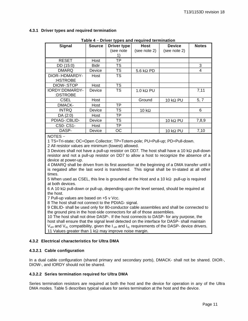
4.3.1 Driver types and required termination
Table 4 −− Driver types and required terminationSignal Source Driver type
(see note1)
Host(see note 2)
Device(see note 2)
Notes
RESET Host TPDD (15:0) Bidir TS 3DMARQ Device TS 5.6 kΩ PD 4
DIOR-:HDMARDY-:HSTROBE
Host TS
DIOW-:STOP Host TSIORDY:DDMARDY-
:DSTROBEDevice TS 1.0 kΩ PU 7,11
CSEL Host Ground 10 kΩ PU 5, 7DMACK- Host TPINTRQ Device TS 10 kΩ 6
DA (2:0) Host TPPDIAG-:CBLID- Device TS 10 kΩ PU 7,8,9
CS0- CS1- Host TPDASP- Device OC 10 kΩ PU 7,10
NOTES −1 TS=Tri-state; OC=Open Collector; TP=Totem-pole; PU=Pull-up; PD=Pull-down.2 All resistor values are minimum (lowest) allowed.3 Devices shall not have a pull-up resistor on DD7. The host shall have a 10 kΩ pull-downresistor and not a pull-up resistor on DD7 to allow a host to recognize the absence of adevice at power-up.4 DMARQ shall be driven from its first assertion at the beginning of a DMA transfer until itis negated after the last word is transferred. This signal shall be tri-stated at all othertimes.5 When used as CSEL, this line is grounded at the Host and a 10 kΩ pull-up is requiredat both devices.6 A 10 kΩ pull-down or pull-up, depending upon the level sensed, should be required atthe host.7 Pull-up values are based on +5 v Vcc.8 The host shall not connect to the PDIAG- signal.9 CBLID- shall be used only for 80-conductor cable assemblies and shall be connected tothe ground pins in the host-side connectors for all of those assemblies.10 The host shall not drive DASP-. If the host connects to DASP- for any purpose, thehost shall ensure that the signal level detected on the interface for DASP- shall maintainVoH and VoL compatibility, given the I oH and IoL requirements of the DASP- device drivers.11 Values greater than 1 kΩ may improve noise margin.
4.3.2 Electrical characteristics for Ultra DMA
4.3.2.1 Cable configuration
In a dual cable configuration (shared primary and secondary ports), DMACK- shall not be shared. DIOR-,DIOW-, and IORDY should not be shared.
4.3.2.2 Series termination required for Ultra DMA
Series termination resistors are required at both the host and the device for operation in any of the UltraDMA modes. Table 5 describes typical values for series termination at the host and the device.

T13/1153D revision 18
Page 12
Table 5 −− Typical series termination for Ultra DMASignal Host Termination Device Termination
DIOR-:HDMARDY-:HSTROBE
22 ohm 82 ohm
DIOW-:STOP 22 ohm 82 ohmCS0-, CS1- 33 ohm 82 ohm
DA0, DA1, DA2 33 ohm 82 ohmDMACK- 22 ohm 82 ohm
DD15 through DD0 33 ohm 33 ohmDMARQ 82 ohm 22 ohmINTRQ 82 ohm 22 ohm
IORDY:DDMARDY-:DSTROBE
82 ohm 22 ohm
RESET- 33 ohm 82 ohmNOTE − Only those signals requiring termination are listed in this table. Ifa signal is not listed, series termination is not required for operation in anUltra DMA mode. Figure 2 shows signals also requiring a pull-up or pull-down resistor at the host. The actual termination values should be selectedto compensate for transceiver and trace impedance to match thecharacteristic cable impedance.
VCC
IORDY DMARQ
DD 7
Figure 2 −− Ultra DMA termination with pull-up or pull-down
T13/1153D revision 18
Page 13
5 Interface signal assignments and descriptions
5.1 Signal summary
The physical interface consists of receivers and drivers communicating through a set of conductors usingan asynchronous interface protocol. Table 6 defines the signal names. For connector descriptions seeannex A. For driver and termination definition see 4.3.1. For signal protocol and timing see clause 9 andclause 10.
Table 6 −− Interface signal name assignmentsDescription Host Dir Dev AcronymCable select (see note) CSELChip select 0 → CS0-Chip select 1 → CS1-Data bus bit 0 ↔ DD0Data bus bit 1 ↔ DD1Data bus bit 2 ↔ DD2Data bus bit 3 ↔ DD3Data bus bit 4 ↔ DD4Data bus bit 5 ↔ DD5Data bus bit 6 ↔ DD6Data bus bit 7 ↔ DD7Data bus bit 8 ↔ DD8Data bus bit 9 ↔ DD9Data bus bit 10 ↔ DD10Data bus bit 11 ↔ DD11Data bus bit 12 ↔ DD12Data bus bit 13 ↔ DD13Data bus bit 14 ↔ DD14Data bus bit 15 ↔ DD15Device active or slave (Device 1) present (see note) DASP-Device address bit 0 → DA0Device address bit 1 → DA1Device address bit 2 → DA2DMA acknowledge → DMACK-DMA request ← DMARQInterrupt request ← INTRQI/O readDMA ready during Ultra DMA data in burstsData strobe during Ultra DMA data out bursts
→→→
DIOR-HDMARDY-HSTROBE
I/O readyDMA ready during Ultra DMA data out burstsData strobe during Ultra DMA data in bursts
←←←
IORDYDDMARDY-DSTROBE
I/O writeStop during Ultra DMA data bursts
→→
DIOW-STOP
Passed diagnosticsCable assembly type identifier
(see note)(see note)
PDIAG-CBLID-
Reset → RESET-NOTE − See signal descriptions and annex A for information on source of these signals
T13/1153D revision 18
Page 14
5.2 Signal descriptions
5.2.1 CS (1:0)- (Chip select)
These are the chip select signals from the host used to select the Command Block registers (see 7.2). WhenDMACK- is asserted, CS0- and CS1- shall be negated and transfers shall be 16-bits wide.
5.2.2 DA (2:0) (Device address)
This is the 3-bit binary coded address asserted by the host to access a register or data port in the device(see 7.2).
5.2.3 DASP- (Device active, device 1 present)
This is a time-multiplexed signal that indicates that a device is active, or that Device 1 is present.
NOTE − The indication that the device is active may be unsynchronized with the executionof the command.
5.2.4 DD (15:0) (Device data)
This is an 8- or 16-bit bi-directional data interface between the host and the device. The lower 8 bits areused for 8-bit register transfers. Data transfers are 16-bits wide.
5.2.5 DIOR-:HDMARDY-:HSTROBE (Device I/O read:Ultra DMA ready:Ultra DMA data strobe)
DIOR- is the strobe signal asserted by the host to read device registers or the data port.
HDMARDY- is a flow control signal for Ultra DMA data in bursts. This signal is asserted by the host toindicate to the device that the host is ready to receive Ultra DMA data in bursts. The host may negateHDMARDY- to pause an Ultra DMA data in burst.
HSTROBE is the data out strobe signal from the host for an Ultra DMA data out burst. Both the rising andfalling edge of HSTROBE latch the data from DD(15:0) into the device. The host may stop generatingHSTROBE edges to pause an Ultra DMA data out burst.
5.2.6 DIOW-:STOP (Device I/O write:Stop Ultra DMA burst)
DIOW- is the strobe signal asserted by the host to write device registers or the data port
DIOW- shall be negated by the host prior to initiation of an Ultra DMA burst. STOP shall be negated by thehost before data is transferred in an Ultra DMA burst. Assertion of STOP by the host during an Ultra DMAburst signals the termination of the Ultra DMA burst.
5.2.7 DMACK- (DMA acknowledge)
This signal shall be used by the host in response to DMARQ to initiate DMA transfers.
5.2.8 DMARQ (DMA request)
This signal, used for DMA data transfers between host and device, shall be asserted by the device when it isready to transfer data to or from the host. For Mulitword DMA transfers, the direction of data transfer iscontrolled by DIOR- and DIOW-. This signal is used in a handshake manner with DMACK-, i.e., the deviceshall wait until the host asserts DMACK- before negating DMARQ, and re-asserting DMARQ if there is moredata to transfer.

T13/1153D revision 18
Page 15
When a DMA operation is enabled, CS0- and CS1- shall not be asserted and transfers shall be 16-bits wide.
5.2.9 INTRQ (Device interrupt)
This signal is used by the selected device to interrupt the host system. When the nIEN bit is cleared to zero,and the device is selected, INTRQ shall be enabled through a tri-state buffer and shall be driven eitherasserted or negated. When the nIEN bit is set to one, or the device is not selected, the INTRQ signal shallbe in a high impedance state.
When asserted, this signal shall be negated by the device within 400 ns of the negation of DIOR- that readsthe Status register. When asserted, this signal shall be negated by the device within 400 ns of the negationof DIOW- that writes the Command register.
When the device is selected by writing to the Device/Head register while an interrupt is pending, INTRQshall be asserted within 400 ns of the negation of DIOW- that writes the Device/Head register. When thedevice is deselected by writing to the Device/Head register while an interrupt is pending, INTRQ shall benegated within 400 ns of the negation of DIOW- that writes the Device/Head register.
For devices implementing the Overlapped feature set, if interrupts are being disabled using nIEN at thesame instant that the device asserts INTRQ, the minimum pulse width of INTRQ should be at least 40 ns.
5.2.10 IORDY:DDMARDY-:DSTROBE (I/O channel ready:Ultra DMA ready:Ultra DMA data strobe)
This signal is negated to extend the host transfer cycle of any host register access (Read or Write) when thedevice is not ready to respond to a data transfer request.
If the device requires to extend the host transfer cycle time at PIO modes 3 and above, the device shallutilize IORDY. Hosts that use PIO modes 3 and above shall support IORDY.
DDMARDY- is a flow control signal for Ultra DMA data out bursts. This signal is asserted by the device toindicate to the host that the device is ready to receive Ultra DMA data out bursts. The device may negateDDMARDY- to pause an Ultra DMA data out burst.
DSTROBE is the data in strobe signal from the device for an Ultra DMA data in burst. Both the rising andfalling edge of DSTROBE latch the data from DD(15:0) into the host. The device may stop generatingDSTROBE edges to pause an Ultra DMA data in burst.
5.2.11 PDIAG-:CBLID- (Passed diagnostics:Cable assembly type identifier)
PDIAG- shall be asserted by Device 1 to indicate to Device 0 that it has completed diagnostics (see clause9).
The host may sample CBLID- after a power-on or hardware reset in order to detect the presence or absenceof an 80-conductor cable assembly by performing the following steps:
a) The host shall wait until the power on or hardware reset sequence is complete for all devices onthe cable;
b) If Device 1 is present, the host should issue IDENTIFY DEVICE or IDENTIFY PACKET DEVICEand use the returned data to determine that Device 1 is compliant with ATA-3 or subsequentstandards. Any device compliant with ATA-3 or subsequent standards releases PDIAG- no laterthan after the first command following a power on or hardware reset sequence.
NOTE − Older devices not in compliance with this standard or ATA-3 may continue toassert this signal providing a false indication of the cable type. Issuing IDENTIFY DEVICEor IDENTIFY PACKET DEVICE not only provides the host with the information required toverify that the devices are compliant with these standards, but also provides a commandresulting in the release of this signal.
T13/1153D revision 18
Page 16
If the host detects that CBLID- is connected to ground, then an 80-conductor cable assembly is installed inthe system. If the host detects that this signal is not connected to ground, then an 80-conductor cableassembly is not installed in the system.
Device 1 Device 0
CBLID-
Host
Open PDIAG- conductor
NOTE − CBLID- is grounded in the 80-conductor cable assembly host connector for thepurpose of indicating to the host that the cable assembly being used is an 80-conductorassembly not a 40-conductor assembly.
Figure 3 −− PDIAG- example using an 80-conductor cable assembly
5.2.12 RESET- (Hardware reset)
This signal, referred to as hardware reset, shall be used by the host to reset the device (see 9.2).
5.2.13 CSEL (Cable select)
The device is configured as either Device 0 or Device 1 depending upon the value of CSEL:
− If CSEL is negated then the device address is 0;− If CSEL is asserted then the device address is 1.
NOTE − Special cabling may be used to selectively ground CSEL e.g., CSEL of Device 0 isconnected to the CSEL conductor in the cable, and is grounded, thus allowing the device torecognize itself as Device 0. CSEL of Device 1 is not connected to CSEL because theconductor is removed, thus the device recognizes itself as Device 1. It should be recognizedthat if a single device is configured at the end of the cable using CSEL, a device 1 onlyconfiguration results.

T13/1153D revision 18
Page 17
Device 0 Device 1
Ground
Host
CSEL conductor
Open
Device 1
Ground
Host
CSEL conductor
Open
Device 0
Ground
Host
CSEL conductor
OpenSee note
NOTE − If a single device configuration is implemented with the device in the middle, a cable stub results that may cause degradation of signals.
Figure 4 −− Cable select example
NOTE − For designated cable assemblies (including all 80-conductor cable assemblies):these assemblies are constructed so that CSEL is connected from the host connector to theconnector at the opposite end of the cable from the host. Therefore, Device 0 shall be at theopposite end of the cable from the host. It should be recognized that if a single device isconfigured at the connector not at the end of the cable, a Device 1 only configurationresults.

T13/1153D revision 18
Page 18
Device 1 Device 0
Ground
Host
CSEL conductor
Open
Device 0
Ground
Host
CSEL conductor
Open
Device 1
Ground
Host
CSEL conductor
OpenSee note
NOTE − If a single device configuration is implemented with the device in the middle, a cable stub results that may cause degradation of signals.
Figure 5 −− Alternate cable select example

T13/1153D revision 18
Page 19
6 General operational requirements
6.1 Command delivery
Commands may be delivered in two forms. For devices that do not implement the PACKET Commandfeature set, all commands and command parameters are delivered by writing the device Command Blockregisters. Such commands are defined as register delivered commands.
Devices that implement the PACKET Command feature set utilize packet delivered commands as well assome register delivered commands.
All register delivered commands and the PACKET command are described in clause 8.
NOTE − The content of command packets delivered by the PACKET command are notdescribed in this specification.
6.2 Register delivered data transfer command sector addressing
For register delivered data transfer commands all addressing of data sectors recorded on the device'smedia is by a logical sector address. There is no implied relationship between logical sector addresses andthe actual physical location of the data sector on the media.
Devices shall support translations as described below:
− All devices shall support LBA translation.− If the device’s capacity is greater than or equal to one sector and less than or equal to
16,514,064 sectors the device shall support CHS translation.− If the device’s capacity is greater than 16,514,064 sectors, then the device may support CHS
translation.− If a device supports CHS translation, then, following a power-on or hardware reset, the CHS
translation enabled by the device shall be known as the default translation.− If a device supports CHS translation, then a device may allow a host to use the INITIALIZE
DEVICE PARAMETERS command to select other CHS translations.− If a device supports CHS translation, then IDENTIFY DEVICE words 1,3, and 6 shall describe
the default translation, and words 53-58 shall describe the current translation.
A CHS address is made up of three fields: the sector number, the head number, and the cylinder number.Sectors are numbered from 1 to the maximum value allowed by the current CHS translation but shall notexceed 255. Heads are numbered from 0 to the maximum value allowed by the current CHS translation butshall not exceed 15. Cylinders are numbered from 0 to the maximum value allowed by the current CHStranslation but cannot exceed 65,535.
When the host selects a CHS translation using the INITIALIZE DEVICE PARAMETERS command, the hostrequests the number of sectors per logical track and the number of heads per logical cylinder. The devicethen computes the number of logical cylinders available in requested translation.
A device shall not change the addressing method specified by the command and shall return statusinformation utilizing the addressing method specified for the command.
1) The host may select either the currently selected CHS translation addressing or LBA addressing ona command-by-command basis by using the LBA bit in the Device/Head register;
2) The device shall support LBA addressing for all media access commands.;

T13/1153D revision 18
Page 20
3) Logical sectors on the device shall be linearly mapped with the first LBA addressed sector (sector 0)being the same sector as the first logical CHS addressed sector (cylinder 0, head 0, sector 1).Irrespective of the logical CHS translation currently in effect, the LBA address of a given logicalsector does not change. The following is always true for LBA numbers less than or equal to16,514,064 for devices supporting the current CHS translation:
( )( )LBA cylinder *heads_ per_ cylinder heads sectors_ per_ track sector= + + −* 1
where heads_per_cylinder and sectors_per_track are the current translation values.
6.2.1 Definitions and value ranges of IDENTIFY DEVICE words (see 8.12)
1) Word 1 shall contain the number of user-addressable logical cylinders in the default CHS translation. Ifthe content of words (61:60) is less than 16,514,064 then the content of word 1 shall be greater than orequal to one and less than or equal to 65,535. If the content of words (61:60) is greater than or equal to16,514,064 then the content of word 1 shall be equal to 16,383.
2) Word 3 shall contain the number of user-addressable logical heads in the default CHS translation. Thecontent of word 3 shall be greater than or equal to one and less than or equal to 16. For compatibilitywith some BIOSs, the content of word 3 may be equal to 15 if the content of word 1 is greater than8192.
3) Word 6 shall contain the number of user-addressable logical sectors in the default CHS translation. Thecontent of word 6 shall be greater than or equal to one and less than or equal to 63.
4) [(The content of word 1) * (the content of word 3) * (the content of word 6)] shall be less than or equal to16,514,064.
5) Word 54 shall contain the number of user-addressable logical cylinders in the current CHS translation.The content of word 54 shall be greater than or equal to one and less than or equal to 65,535. Afterpower-on or after a hardware reset the content of word 54 shall be equal to the content of word 1.
6) Word 55 shall contain the number of user-addressable logical heads in the current CHS translation. Thecontent of word 55 shall be greater than or equal to one and less than or equal to 16. After power-on orafter a hardware reset the content of word 55 shall be equal to the content of word 3.
7) Word 56 shall contain the number of user-addressable logical sectors in the current CHS translation.The content of word 56 should be equal to 63 for compatibility with all BIOSs. However, the content ofword 56 may be greater than or equal to one and less than or equal to 255. At power-on or after ahardware reset the content of word 56 shall equal the content of word 6.
8) Words (58:57) shall contain the user-addressable capacity in sectors for the current CHS translation.The content of words (58:57) shall equal [(the content of word 54) * (the content of word 55) * (thecontent of word 56)]. The content of words (58:57) shall be less than or equal to 16,514,064. Thecontent of words (58:57) shall be less than or equal to the content of words (61:60).
9) The content of words 54, 55, 56, and (58:57) may be affected by the host issuing an INITIALIZEDEVICE PARAMETERS command (see 8.16).
10) If the content of words (61:60) is greater than 16,514,064 and if the device does not support CHSaddressing, then the content of words 1, 3, 6, 54, 55, 56, and (58:57) shall equal zero. If the content ofword 1, word 3, or word 6 equals zero, then the content of words 1, 3, 6, 54, 55, 56, and (58:57) shallequal zero.
11) Words (61:60) shall contain the total number of user-addressable sectors. The content of words (61:60)shall be greater than or equal to one and less than or equal to 268,435,456.
12) The content of words 1, 54, (58:57), and (61:60) may be affected by the host issuing a SET MAXADDRESS command (see 8.38).
6.2.2 Addressing constraints and error reporting
1) Devices may access any address in the current CHS translation if [(the requested cylinder +1) * (therequested head + 1) * (the requested sector)] is less than or equal to the content of words (61:60).
2) Devices may respond with an “ID NOT FOUND” or a command aborted error to any command with aCHS address request where one or more of the following are true:
3) The requested cylinder value is greater than [(the content of word 54) - 1]4) The requested head value is greater than [(the content of word 55) - 1]

T13/1153D revision 18
Page 21
5) The requested sector value is zero or greater than the content of word 566) Devices shall respond with an “ID NOT FOUND” or a command aborted error to any command with an
LBA address request where the requested LBA number is greater than or equal to the content of words(61:60).
6.3 General feature set
The General feature set defines the common commands implemented by devices.
6.3.1 General feature set for devices not implementing the PACKET command feature set
The following General feature set commands are mandatory for all devices not implementing the PACKETcommand feature set:
− EXECUTE DEVICE DIAGNOSTIC− IDENTIFY DEVICE− INITIALIZE DEVICE PARAMETERS− READ DMA− READ MULTIPLE− READ SECTOR(S)− READ VERIFY SECTOR(S)− SEEK− SET FEATURES− SET MULTIPLE MODE− WRITE DMA− WRITE MULTIPLE− WRITE SECTOR(S)
The following General feature set commands are optional for devices not implementing the PACKETcommand feature set:
− DOWNLOAD MICROCODE− FLUSH CACHE− NOP− READ BUFFER− WRITE BUFFER
Read only devices shall return command aborted in response to write commands.
The following General feature set command is prohibited for use by devices not implementing the PACKETcommand feature set:
− DEVICE RESET
The following resets are mandatory for devices not implementing the PACKET command feature set:
− Power On Reset: Executed at power on, the device executes a series of electrical circuitrydiagnostics, spins up the HDA, tests speed and other mechanical parametrics, and sets defaultvalues (see 9.2).
− Hardware Reset: Executed in response to the assertion of the RESET- signal the deviceexecutes a series of electrical circuitry diagnostics, and resets to default values (see 9.2).
− Software Reset: Executed in response to the setting of the SRST bit in the Device Controlregister the device resets the interface circuitry (see 9.3).

T13/1153D revision 18
Page 22
6.3.2 General feature set for devices implementing the PACKET command feature set
The following General feature set commands are mandatory for all devices implementing the PACKETcommand feature set:
− DEVICE RESET− EXECUTE DEVICE DIAGNOSTIC− IDENTIFY DEVICE− IDENTIFY PACKET DEVICE− NOP− READ SECTOR(S)− SET FEATURES
The following General command set commands are optional for devices implementing the PACKETcommand feature set:
− FLUSH CACHE
The following General command set commands are prohibited for use by devices implementing thePACKET command feature set.
− DOWNLOAD MICROCODE− INITIALIZE DEVICE PARAMETERS− READ BUFFER− READ DMA− READ MULTIPLE− READ VERIFY− SEEK− SET MULTIPLE MODE− WRITE BUFFER− WRITE DMA− WRITE MULTIPLE− WRITE SECTOR(S)
The following resets are mandatory for devices implementing the PACKET command feature set:− Power On Reset: Executed at power on, the device executes a series of electrical circuitry
diagnostics, spins up the HDA, tests speed and other mechanical parametrics, and sets defaultvalues (see 9.2).
− Hardware Reset: Executed in response to the assertion of the RESET- signal the deviceexecutes a series of electrical circuitry diagnostics, and resets to default values (see 9.2).
− Software Reset: Executed in response to the setting of the SRST bit in the Device Controlregister the device resets the interface circuitry (see 9.3).
− Device Reset: Executed in response to the DEVICE RESET command the device resets theinterface circuitry (see 8.7).
6.4 Ultra DMA feature set
6.4.1 Overview
Ultra DMA is a data transfer protocol used with the READ DMA, WRITE DMA, READ DMA QUEUED,WRITE DMA QUEUED, and PACKET commands. When this protocol is enabled it shall be used instead ofthe Multiword DMA protocol when these commands are issued by the host. This protocol applies to theUltra DMA data burst only. When this protocol is used there are no changes to other elements of the ATAprotocol (e.g., Command Block Register access).
Several signal lines are redefined to provide new functions during an Ultra DMA burst. These lines assumethese definitions when:1) an Ultra DMA mode is selected, and
T13/1153D revision 18
Page 23
2) a host issues a READ DMA, WRITE DMA, READ DMA QUEUED, WRITE DMA QUEUED, or a PACKETcommand requiring data transfer, and3) the host asserts DMACK-.These signal lines revert back to the definitions used for non-Ultra DMA transfers upon the negation ofDMACK- by the host at the termination of an Ultra DMA burst. All of the control signals are unidirectional.DMARQ and DMACK- retain their standard definitions.
With the Ultra DMA protocol, the control signal (STROBE) that latches data from DD(15:0) is generated bythe same agent (either host or device) that drives the data onto the bus. Ownership of DD(15:0) and thisdata strobe signal are given either to the device during an Ultra DMA data in burst or to the host for an UltraDMA data out burst.
During an Ultra DMA burst a sender shall always drive data onto the bus, and, after a sufficient time to allowfor propagation delay, cable settling, and setup time, the sender shall generate a STROBE edge to latch thedata. Both edges of STROBE are used for data transfers so that the frequency of STROBE is limited to thesame frequency as the data. The highest fundamental frequency on the cable shall be 16.67 milliontransitions per second or 8.33 MHz (the same as the maximum frequency for PIO mode 4 and DMA mode2).
Words in the IDENTIFY DEVICE data indicate support of the Ultra DMA feature and the Ultra DMA modesthe device is capable of supporting. The Set transfer mode subcommand in the SET FEATURES commandshall be used by a host to select the Ultra DMA mode at which the system operates. The Ultra DMA modeselected by a host shall be less than or equal to the fastest mode of which the device is capable. Only oneUltra DMA mode shall be selected at any given time. All timing requirements for a selected Ultra DMAmode shall be satisfied. Devices supporting Ultra DMA mode 2 shall also support Ultra DMA modes 0 and1. Devices supporting Ultra DMA mode 1 shall also support Ultra DMA mode 0.
An Ultra DMA capable device shall retain its previously selected Ultra DMA mode after executing aSoftware reset sequence or the sequence caused by receipt of a DEVICE RESET command. An Ultra DMAcapable device shall clear any previously selected Ultra DMA mode and revert to its default non-Ultra DMAmodes after executing a Power on or hardware reset.
Both the host and device perform a CRC function during an Ultra DMA burst. At the end of an Ultra DMAburst the host sends the its CRC data to the device. The device compares its CRC data to the data sentfrom the host. If the two values do not match the device reports an error in the error register at the end ofthe command. If an error occurs during one or more Ultra DMA bursts for any one command, at the end ofthe command, the device shall report the first error that occurred.
6.4.2 Phases of operation
An Ultra DMA data transfer is accomplished through a series of Ultra DMA data in or data out bursts. EachUltra DMA burst has three mandatory phases of operation: the initiation phase, the data transfer phase, andthe Ultra DMA burst termination phase. In addition, an Ultra DMA burst may be paused during the datatransfer phase (see 9.13 and 9.14 for the detailed protocol descriptions for each of these phases, 10.2.4defines the specific timing requirements). In the following rules DMARDY- is used in cases that could applyto either DDMARDY- or HDMARDY-, and STROBE is used in cases that could apply to either DSTROBE orHSTROBE. The following are general Ultra DMA rules.
1) An Ultra DMA burst is defined as the period from an assertion of DMACK- by the host to the subsequentnegation of DMACK-.
2) A recipient shall be prepared to receive at least two data words whenever it enters or resumes an UltraDMA burst.
6.4.2.1 Ultra DMA burst initiation phase rules
1) An Ultra DMA burst initiation phase begins with the assertion of DMARQ by a device and ends when thesender generates a STROBE edge to transfer the first data word.
2) An Ultra DMA burst shall always be requested by a device asserting DMARQ.

T13/1153D revision 18
Page 24
3) A host indicates it is ready to initiate the requested Ultra DMA burst by asserting DMACK-.4) A host shall never assert DMACK- without first detecting that DMARQ is asserted.5) For Ultra DMA data in bursts: a device may begin driving DD(15:0) after detecting that DMACK- is
asserted, STOP negated, and HDMARDY- is asserted.6) After asserting DMARQ or asserting DDMARDY- for an Ultra DMA data out burst, a device shall not
negate either signal until the first STROBE edge is generated.7) After negating STOP or asserting HDMARDY- for an Ultra DMA data in burst, a host shall not change
the state of either signal until the first STROBE edge is generated.
6.4.2.2 Data transfer phase rules
1) The data transfer phase is in effect from after Ultra DMA burst initiation until Ultra DMA bursttermination.
2) A recipient pauses an Ultra DMA burst by negating DMARDY- and resumes an Ultra DMA burst byreasserting DMARDY-.
3) A sender pauses an Ultra DMA burst by not generating STROBE edges and resumes by generatingSTROBE edges.
4) A recipient shall not signal a termination request immediately when the sender stops generatingSTROBE edges. In the absence of a termination from the sender the recipient shall always negateDMARDY- and wait the required period before signaling a termination request.
5) A sender may generate STROBE edges at greater than the minimum period specified by the enabledUltra DMA mode. The sender shall not generate STROBE edges at less than the minimum periodspecified by the enabled Ultra DMA mode. A recipient shall be able to receive data at the minimumperiod specified by the enabled Ultra DMA mode.
6.4.2.3 Ultra DMA burst termination phase rules
1) Either a sender or a recipient may terminate an Ultra DMA burst.2) Ultra DMA burst termination is not the same as command completion. If an Ultra DMA burst termination
occurs before command completion, the command shall be completed by initiation of a new Ultra DMAburst at some later time or aborted by the host issuing a hardware or software reset to the device.
3) An Ultra DMA burst shall be paused before a recipient requests a termination.4) A host requests a termination by asserting STOP. A device acknowledges a termination request by
negating DMARQ.5) A device requests a termination by negating DMARQ. A host acknowledges a termination request by
asserting STOP.6) Once a sender requests a termination, it shall not change the state of STROBE until the recipient
acknowledges the request. Then, if STROBE is not in the asserted state, the sender shall returnSTROBE to the asserted state. No data shall be transferred on this transition of STROBE.
7) A sender shall return STROBE to the asserted state whenever it detects a termination request from therecipient. No data shall be transferred nor CRC calculated on this edge of DSTROBE.
8) Once a recipient requests a termination, it shall not change DMARDY from the negated state for theremainder of an Ultra DMA burst.
9) A recipient shall ignore a STROBE edge when DMARQ is negated or STOP is asserted.
6.5 PACKET Command feature set
The PACKET Command feature set provides for devices that require command parameters that are tooextensive to be expressed in the Command Block registers. Devices implementing the PACKET Commandfeature set exhibit responses different from that exhibited by devices not implementing this feature set.
The commands unique to the PACKET Command feature set are:
− PACKET− IDENTIFY PACKET DEVICE
T13/1153D revision 18
Page 25
6.5.1 Identification of PACKET Command feature set devices
When executing a power on, hardware, DEVICE RESET, or software reset, a device implementing thePACKET Command feature set performs the same reset protocol as other devices but leaves the registerswith a signature unique to PACKET Command feature set devices (see 9.1).
In addition, the IDENTIFY DEVICE command shall not be executed but shall be command aborted and shallreturn a signature unique to devices implementing the PACKET Command feature set. The IDENTIFYPACKET DEVICE command is used by the host to get identifying parameter information for a deviceimplementing the PACKET Command feature set (see 8.12.5.2 and 8.13).
6.5.2 PACKET Command feature set resets
Devices implementing the PACKET Command feature set respond to power-on, hardware, and softwareresets as any other device except for the resulting contents in the device registers as described above.However, software reset should not be issued while a PACKET command is in progress. PACKETcommands utilized by some devices do not terminate if a software reset is issued.
The DEVICE RESET command is provided to allow the device to be reset without effecting the other deviceon the bus.
6.5.3 The PACKET command
The PACKET command allows a host to send a command to the device via a command packet. Thecommand packet contains the command and command parameters that the device is to execute.
Upon receipt of the PACKET command the device sets BSY to one and prepares to receive the commandpacket. When ready, the device sets DRQ to one and clears BSY to zero. The command packet is thentransferred to the device by PIO transfer. When the last word of the command packet is transferred, thedevice sets BSY to one, and clears DRQ to zero (see 8.21 and 9.11).
6.6 Overlapped feature set
Overlap allows devices that require extended command time to perform a bus release so that the otherdevice on the bus may be used. To perform a bus release the device shall clear both DRQ and BSY to zero.When selecting the other device during overlapped operations, the host shall disable interrupts via the nIENbit on the currently selected device before writing the Device/Head register to select the other device.
The only commands that may be overlapped are:
− NOP (with 01h subcommand code)− PACKET− READ DMA QUEUED− SERVICE− WRITE DMA QUEUED
For the PACKET command, overlap is indicated by the OVL bit in the Features register when the PACKETcommand is issued.
If the device supports PACKET command overlap, the OVL bit is set to one in the Features register and theRelease interrupt has been enabled via the SET FEATURES command, then the device shall perform a busrelease when the command packet has been received. This allows the host to select the other device toexecute commands if desired. When the device is ready to continue the command, the device sets SERV toone, and asserts INTRQ if selected and interrupts are enabled. The host then issues the SERVICEcommand to continue the execution of the command
If the device supports PACKET command overlap, the OVL bit is set to one in the Features register and theRelease interrupt has been disabled via the SET FEATURES command, then the device may or may not
T13/1153D revision 18
Page 26
perform a bus release. If the device is ready to complete execution of the command, it may complete thecommand immediately as described in the non-overlap case. If the device is not ready to completeexecution of the command, the device may perform a bus release and complete the command as describedin the previous paragraph.
For the READ DMA QUEUED and WRITE DMA QUEUED commands, the device may or may not performa bus release. If the device is ready to complete execution of the command, it may complete the commandimmediately. If the device is not ready to complete execution of the command, the device may perform abus release and complete the command via a service request.
If a device has an outstanding command that has been released, it can only indicate that it requires to beserviced when it is selected. This implies that the host has to poll each device to determine if a device isrequesting service. The polling can be performed at the host either by hardware or by a software routine.The latter implies a considerable host processor overhead. Hardware polling is initiated by the NOP AutoPoll command.
The NOP Auto Poll command is a host adapter function and is ignored by the device. The host software cantest for the support of this feature by issuing the NOP Auto Poll command and examining the Statusregister. If the host adapter does not support this feature, the response received by the host will be from thedevice with the ERR bit set to one. If the host adapter does support the command, the response will be fromthe host adapter with the ERR bit cleared to zero. The only action taken by a device supporting theOverlapped feature set will be to return the error indication in the Status register and to not abort anyoutstanding commands.
6.7 Queued feature set
Command queuing allows the host to issue concurrent commands to the same device. Only commandsincluded in the overlapped feature set may be queued. If a queue exists when a non-queued command isreceived, the non-queued command shall be command aborted and the commands in the queue shall bediscarded. The ending status shall be command aborted and the results are indeterminate.
The maximum queue depth supported by a device shall be indicated in word 75 of the IDENTIFY DEVICEor IDENTIFY PACKET DEVICE response.
A queued command shall have a Tag provided by the host in the Sector Count register to uniquely identifythe command. When the device restores register parameters during the execution of the SERVICEcommand, this Tag shall be restored so that the host may identify the command for which status is beingpresented. If a queued command is issued with a Tag value that is identical to the Tag value for a commandalready in the queue, the entire queue shall be aborted including the new command. The ending status shallbe command aborted and the results are indeterminate. If any error occurs, the command queue shall beaborted.
When the device is ready to continue the processing of a bus released command and BSY and DRQ areboth cleared to zero, the device requests service by setting SERV to one, setting a pending interrupt, andasserting INTRQ if selected and if nIEN is cleared to zero. SERV shall remain set until all commands readyfor service have been serviced. The pending interrupt shall be cleared and INTRQ negated by a Statusregister read or a write to the Command register.
When the device is ready to continue the processing of a bus released command and BSY or DRQ is set toone (i.e., the device is processing another command on the bus), the device requests service by settingSERV to one. SERV shall remain set until all commands ready for service have been serviced. At commandcompletion of the current command processing (i.e., when both BSY and DRQ are cleared to zero), thedevice shall process interrupt pending and INTRQ per the protocol for the command being completed. Noadditional interrupt shall occur due to other commands ready for service until after the device’s SERV bithas been cleared to zero.
When the device receives a new command while queued commands are ready for service, the device shallexecute the new command and process interrupt pending and INTRQ per the protocol for the new

T13/1153D revision 18
Page 27
command. If the queued commands ready for service still exist at command completion of this command,SERV remains set to one but no additional interrupt shall occur due to commands ready for service.
When queuing commands, the host shall disable interrupts via the nIEN bit before writing a new commandto the Command register and may re-enable interrupts after writing the command. When reading status atcommand completion of a command, the host shall check the SERV bit since the SERV bit may be setbecause the device is ready for service associated with another command. The host receives no additionalinterrupt to indicate that a queued command is ready for service.
6.8 Power Management feature set
A device shall implement power management. A device implementing the PACKET Command feature setmay implement the power management as defined by the packet command set implemented by the device.Otherwise, the device shall implement the Power Management feature set as described in this standard.
The Power Management feature set permits a host to modify the behavior of a device in a manner thatreduces the power required to operate. The Power Management feature set provides a set of commandsand a timer that enable a device to implement low power consumption modes. A register deliveredcommand device that implements the Power Management feature set shall implement the followingminimum set of functions:
− A Standby timer− CHECK POWER MODE command− IDLE command− IDLE IMMEDIATE command− SLEEP command− STANDBY command− STANDBY IMMEDIATE command
A device that implements the PACKET Command feature set and implements the Power Managementfeature set shall implement the following minimum set of functions:
− A Standby timer− CHECK POWER MODE command− IDLE IMMEDIATE command− SLEEP command− STANDBY IMMEDIATE command
6.8.1 Power modes
In Active mode the device is capable of responding to commands. During the execution of a media accesscommand a device shall be in Active mode. Power consumption is greatest in this mode.
In Idle mode the device is capable of responding to commands but the device may take longer to completecommands than when in the Active mode. Power consumption may be reduced from that of Active mode.
In Standby mode the device is capable of responding to commands but the device may take longer tocomplete commands than in the Idle mode. The time to respond could be as long as 30 s. Powerconsumption may be reduced from that of Idle mode.
In Sleep mode the device requires a hardware or software reset to be activated. The time to respond couldbe as long as 30 s. Sleep mode provides the lowest power consumption of any mode.
6.8.2 Power management commands

T13/1153D revision 18
Page 28
The CHECK POWER MODE command allows a host to determine if a device is currently in, going to orleaving Standby or Idle mode. The CHECK POWER MODE command shall not change the power mode oraffect the operation of the Standby timer.
The IDLE and IDLE IMMEDIATE commands move a device to Idle mode immediately from the Active orStandby modes. The IDLE command also sets the Standby timer count and enables or disables theStandby timer.
The SLEEP command moves a device to Sleep mode. The device's interface becomes inactive atcommand completion of the SLEEP command. A hardware or software reset or DEVICE RESET commandis required to move a device out of Sleep mode.
After receiving a reset, the device should return to the power mode it was in before receiving the reset,unless the device was in the Sleep mode. If the device was in the Sleep mode when receiving a reset, thedevice should return to the Standby mode (This may be made a mandatory requirement in a futurestandard).
The STANDBY and STANDBY IMMEDIATE commands move a device to Standby mode immediately fromthe Active or Idle modes. The STANDBY command also sets the Standby timer count and enables ordisables the Standby timer.
6.8.3 Standby timer
The Standby timer provides a method for the device to automatically enter Standby mode from either Activeor Idle mode following a host programmed period of inactivity. If the Standby timer is enabled and if thedevice is in the Active or Idle mode, the device waits for the specified time period and if no command isreceived, the device automatically enters the Standby mode.
If the Standby timer is disabled, the device may not automatically enter Standby mode.
6.8.4 Idle mode transition
If a device accepts the IDLE IMMEDIATE command, the device shall transition to the Idle mode afterreceipt of the command. If the device accepts the IDLE command it shall transition to the Idle mode asdescribed in 8.14.8. Some devices may perform internal power management and transition to the Idlemode without host intervention.
6.8.5 Status
In Sleep mode, the device's interface is not active. The content of the Status register is invalid in this mode.
6.8.6 Power mode transitions
Figure 6 shows the minimum set of mode transitions that shall be implemented.

T13/1153D revision 18
Page 29
1 Active 34 4
5
Idle2
3 Standby
5 5 Sleep
Resets 6 6
(see path 6)
Path 1: An IDLE command, IDLE IMMEDIATE command, or vendor specific implementation moves the device to Idle mode.Path 2: An IDLE command or IDLE IMMEDIATE command moves the device to Idle mode.Path 3: A STANDBY command, STANDBY IMMEDIATE command, vendor specific implementation, or Standby timer expiration moves the device to Standby mode.Path 4: A Media access command moves the device to Active mode.Path 5: A SLEEP command moves the device to Sleep mode.Path 6: A reset, either hardware, software, or DEVICE RESET command moves the device to Active, Idle or Standby as specified by the device vendor.
Figure 6 −− Power management modes
6.9 Advanced Power Management feature set
The Advanced Power Management feature set is an optional feature set that allows the host to select apower management level. The power management level is a scale from the lowest power consumptionsetting of 01h to the maximum performance level of FEh. Device performance may increase with increasingpower management levels. Device power consumption may increase with increasing power managementlevels. The power management levels may contain discrete bands. For example, a device may implementone power management method from level 80h to A0h and a higher performance, higher powerconsumption method from level A1h to FEh. Advanced power management levels 80h and higher do notpermit the device to spin down to save power.
The Advanced Power Management feature set uses the following functions:− A SET FEATURES subcommand to enable Advanced Power Management− A SET FEATURES subcommand to disable Advanced Power Management
Advanced Power Management is independent of the Standby timer setting. If both Advanced PowerManagement and the Standby timer are set, the device will go to the Standby state when the timer times outor the device’s Advanced Power Management algorithm indicates that it is time to enter the Standby state.
The IDENTIFY DEVICE word 83, bit 3 indicates that Advanced Power Management is supported if set. word86, bit 3 indicates that Advanced Power Management is enabled if set. Word 91, bits (7:0) contain thecurrent advanced power management level if Advanced Power Management is enabled.

T13/1153D revision 18
Page 30
6.10 Security Mode feature set
The Security Mode feature set allows a host to implement a security password system to preventunauthorized access to the internal disk drive.
A device that implements the Security Mode feature set shall implement the following minimum set ofcommands:
− SECURITY SET PASSWORD− SECURITY UNLOCK− SECURITY ERASE PREPARE− SECURITY ERASE UNIT− SECURITY FREEZE LOCK− SECURITY DISABLE PASSWORD
Support of the Security Mode feature set is indicated in IDENTIFY DEVICE word 128.
6.10.1 Security mode default setting
The Master password shall be set to a vendor specific value during manufacturing and the Lock modedisabled.
The system manufacturer/dealer may set a new Master password using the SECURITY SET PASSWORDcommand, without enabling or disabling the Lock mode.
6.10.2 Initial setting of the User password
When a User password is set, the device shall automatically enter Lock mode the next time the device ispowered-on or after a hardware reset.
6.10.3 Security mode operation from power-on or hardware reset
When Lock is enabled, the device rejects media access commands until a SECURITY UNLOCK commandis successfully completed.
6.10.4 Frozen mode
The SECURITY FREEZE LOCK command places the device in Frozen mode. This prevents accidental ormalicious password activation or setting. Table 7 lists the commands that the device shall execute when inFrozen mode. The device shall exit Frozen mode on power off. All devices that support the Security Modefeature set should be issued a SECURITY FREEZE LOCK command during system initialization.
6.10.5 User password lost
If the User password does not match and High level security is set, the device shall not allow the user toaccess data. The device shall be unlocked using the Master password.
If the User password is lost and Maximum security level is set, data access shall not be allowed. However,the SECURITY ERASE UNIT command shall unlock the device and shall erase all user data if the Masterpassword matches.
6.10.6 Attempt limit for SECURITY UNLOCK command
The device shall have an attempt limit counter. The purpose of this counter is to defeat repeated trialattacks. After each failed User or Master password SECURITY UNLOCK command, the counter isdecremented. When the counter value reaches zero the EXPIRE bit (bit 4) of word 128 in the IDENTIFYDEVICE information is set, and the SECURITY UNLOCK and SECURITY UNIT ERASE commands are

T13/1153D revision 18
Page 31
command aborted until the device is powered off or hardware reset. The EXPIRE bit shall be cleared to zeroafter power on or hardware reset. The counter shall be set to five after a power on or hardware reset.
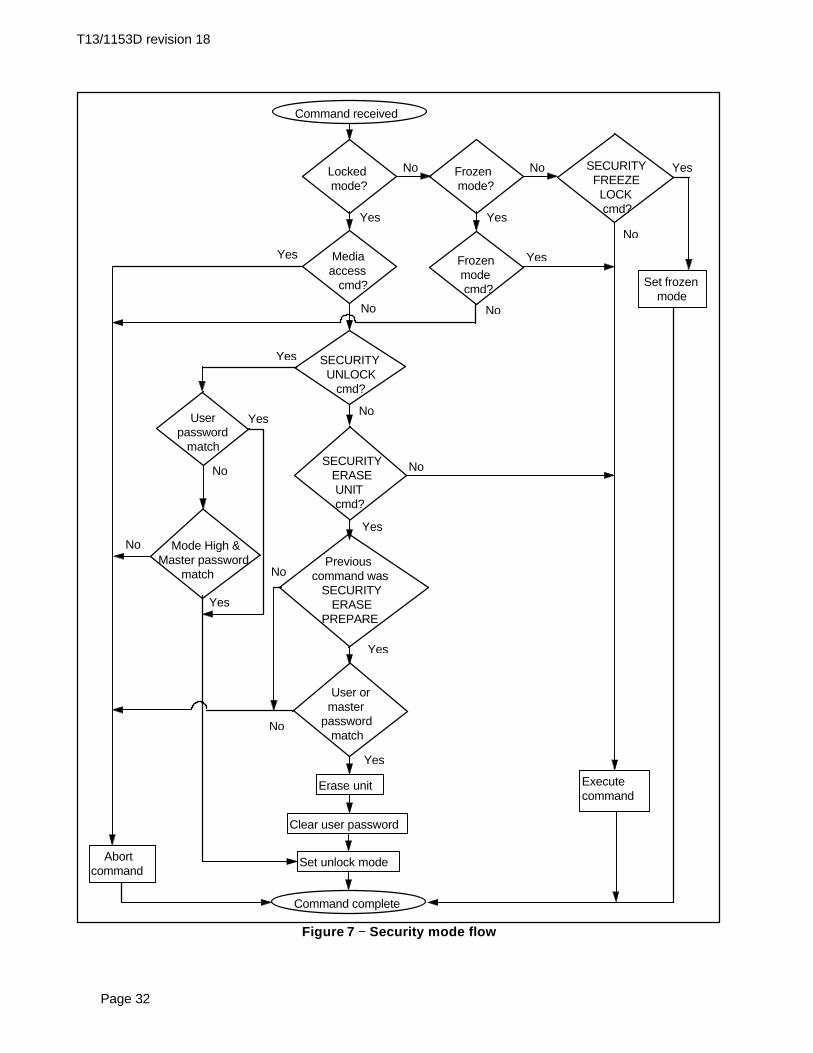
T13/1153D revision 18
Page 32
No
Command received
Frozen mode?
Yes
NoLocked mode?
Yes
No
Yes Mediaaccess cmd?
No
SECURITY ERASE UNIT cmd?
Yes
No
Previouscommand was SECURITY ERASE PREPARE
Yes
No
Set frozen mode
SECURITY FREEZE LOCK cmd?
Yes
No
Frozen mode cmd?
Yes
No
Mode High &Master password match
Yes
Userpassword match
No
SECURITY UNLOCK cmd?
Yes
NoYes
User or master password match
Yes
No
Erase unit
Clear user password
Set unlock mode
Command complete
Abortcommand
Executecommand
Figure 7 −− Security mode flow

T13/1153D revision 18
Page 33
Table 7 −− Security mode command actionsCommand Locked mode Unlocked
modeFrozen mode
CHECK POWER MODE Executable Executable ExecutableCFA REQUEST EXTENDED ERROR CODE Executable Executable Executable
CFA ERASE SECTORS Command aborted Executable ExecutableCFA TRANSLATE SECTOR Executable Executable Executable
CFA WRITE MULTIPLE WITHOUT ERASE Command aborted Executable ExecutableCFA WRITE SECTORS WITHOUT ERASE Command aborted Executable Executable
DEVICE RESET Executable Executable ExecutableDOWNLOAD MICROCODE Executable Executable Executable
EXECUTE DEVICE DIAGNOSTIC Executable Executable ExecutableFLUSH CACHE Command aborted Executable Executable
GET MEDIA STATUS Command aborted Executable ExecutableIDENTIFY DEVICE Executable Executable Executable
IDENTIFY PACKET DEVICE Executable Executable ExecutableIDLE Executable Executable Executable
IDLE IMMEDIATE Executable Executable ExecutableINITIALIZE DEVICE PARAMETERS Executable Executable Executable
MEDIA EJECT Command aborted Executable ExecutableMEDIA LOCK Command aborted Executable Executable
MEDIA UNLOCK Command aborted Executable ExecutableNOP Executable Executable Executable
PACKET Command aborted Executable ExecutableREAD BUFFER Executable Executable Executable
READ DMA Command aborted Executable ExecutableREAD DMA QUEUED Command aborted Executable Executable
READ MULTIPLE Command aborted Executable ExecutableREAD NATIVE MAX ADDRESS Executable Executable Executable
READ SECTORS Command aborted Executable ExecutableREAD VERIFY SECTORS Command aborted Executable Executable
SECURITY DISABLE PASSWORD Command aborted Executable Command abortedSECURITY ERASE PREPARE Executable Executable Executable
SECURITY ERASE UNIT Executable Executable Command abortedSECURITY FREEZE LOCK Command aborted Executable Executable
SECURITY SET PASSWORD Command aborted Executable Command abortedSECURITY UNLOCK Executable Executable Command aborted
SEEK Executable Executable ExecutableSERVICE Command aborted Executable Executable
SET FEATURES Executable Executable ExecutableSET MAX ADDRESS Command aborted Executable Executable
SET MULTIPLE MODE Executable Executable ExecutableSLEEP Executable Executable Executable
SMART DISABLE OPERATIONS Executable Executable ExecutableSMART ENABLE/DISABLE AUTOSAVE Executable Executable Executable
SMART ENABLE OPERATIONS Executable Executable ExecutableSMART EXECUTE OFF-LINE IMMEDIATE Executable Executable Executable
SMART READ DATA Executable Executable ExecutableSMART RETURN STATUS Executable Executable Executable
SMART SAVE ATTRIBUTE VALUES Executable Executable ExecutableSTANDBY Executable Executable Executable
STANDBY IMMEDIATE Executable Executable ExecutableWRITE BUFFER Executable Executable Executable
WRITE DMA Command aborted Executable ExecutableWRITE DMA QUEUED Command aborted Executable Executable
WRITE MULTIPLE Command aborted Executable ExecutableWRITE SECTORS Command aborted Executable Executable

T13/1153D revision 18
Page 34
6.11 Self-monitoring, analysis, and reporting technology feature set
The intent of self-monitoring, analysis, and reporting technology (the SMART feature set) is to protect userdata and minimize the likelihood of unscheduled system downtime that may be caused by predictabledegradation and/or fault of the device. By monitoring and storing critical performance and calibrationparameters, SMART feature set devices attempt to predict the likelihood of near-term degradation or faultcondition. Providing the host system the knowledge of a negative reliability condition allows the host systemto warn the user of the impending risk of a data loss and advise the user of appropriate action. Support ofthis feature set is indicated in bit 0 of IDENTIFY DEVICE word 82.
Devices that implement the PACKET Command feature set shall not implement the SMART feature set asdescribed in this subclause. Devices that implement the PACKET Command feature set and SMART shallimplement SMART as defined by the command packet set implemented by the device.
6.11.1 Device SMART data structure
SMART feature set capability and status information for the device are stored in the device SMART datastructure. The off-line data collection capability and status data stored herein may be useful to the host if theSMART EXECUTE OFF-LINE IMMEDIATE command is implemented (see 8.41.4).
6.11.2 On-line data collection
Collection of SMART data in an “on-line” mode shall have no impact on device performance. The SMARTdata that is collected or the methods by which data is collected in this mode may be different than those inthe off-line data collection mode for any particular device and may vary from one device to another.
6.11.3 Off-line data collection
The device shall use its off-line mode for data collection routines that have an impact on performance if thedevice is required to respond to commands from the host while performing that data collection. This impacton performance may vary from device to device. The data that is collected or the methods by which thedata is collected in this mode may be different than those in the on-line data collection mode for anyparticular device and may vary from one device to another.
6.11.4 Threshold exceeded condition
This condition occurs when the device’s SMART reliability status indicates an impending degrading or faultcondition.
6.11.5 SMART feature set commands
These commands use a single command code and are differentiated from one another by the value placedin the Features register (see 8.41).
If the SMART feature set is implemented, the following commands shall be implemented.
− SMART DISABLE OPERATIONS− SMART ENABLE/DISABLE AUTOSAVE− SMART ENABLE OPERATIONS− SMART RETURN STATUS
If the SMART feature set is implemented, the following commands may be implemented.
− SMART EXECUTE OFF-LINE IMMEDIATE− SMART READ DATA

T13/1153D revision 18
Page 35
6.11.6 SMART operation with power management modes
When used with a host that has implemented the Power Management feature set, a SMART enabled deviceshould automatically save its accumulated SMART data upon receipt of an IDLE IMMEDIATE, STANDBYIMMEDIATE, or SLEEP command or upon return to an Active or Idle mode from a Standby mode (see8.41.5).
If a SMART feature set enabled device has been set to utilize its Standby timer, the device shouldautomatically save its accumulated SMART data prior to going from an Idle mode to the Standby mode orupon return to an Active or Idle mode from a Standby mode.
A device shall not execute any routine to automatically save its accumulated SMART data while the deviceis in a Standby or Sleep mode.
6.12 Host Protected Area feature set
A reserved area for data storage outside the normal operating system file system is required for severalspecialized applications. Systems may wish to store configuration data or save memory to the device in alocation that the operating systems cannot change. The Host Protected Area feature set allows a portion ofthe device to be reserved for such an area when the device is initially configured. A device that implementsthe Host Protected Area feature set shall implement the following minimum set of commands:
− READ NATIVE MAX ADDRESS− SET MAX ADDRESS
If the Host Protected Area feature set is supported, the device shall indicate so by setting bit 10 ofIDENTIFY DEVICE word 82.
The READ NATIVE MAX ADDRESS command allows the host to determine the maximum native addressspace of the device even when a protected area has been allocated.
The SET MAX ADDRESS command allows the host to redefine the maximum address of the useraccessible address space. That is, when the SET MAX ADDRESS command is issued with a maximumaddress less than the native maximum address, the device reduces the user accessible address space tothe maximum set, providing a protected area above that maximum address. The SET MAX ADDRESScommand shall be immediately preceded by a READ NATIVE MAX ADDRESS command. After the SETMAX ADDRESS command has been issued, the device shall report only the reduced user address space inresponse to an IDENTIFY DEVICE command in words 1, 54, 57, 58, 60, and 61. Any read or writecommand to an address above the maximum address specified by the SET MAX ADDRESS command shallcause command completion with the IDNF bit set to one and ERR set to one, or command aborted. Avolatility bit in the Sector Count register allows the host to specify if the maximum address set is preservedacross power-up or hardware reset cycles. On power up or hardware reset the device maximum addressreturns to the last non-volatile address setting regardless of subsequent volatile SET MAX ADDRESScommands. If the SET MAX ADDRESS command is issued with a value that exceeds the native maximumaddress command aborted shall be returned.
T13/1153D revision 18
Page 36
Typical use of these commands would be:
On Reseta) BIOS receives control after a system reset;b) BIOS issues a READ NATIVE MAX ADDRESS command to find the max capacity of the
device;c) BIOS issues a SET MAX ADDRESS command to the values returned by READ NATIVE MAX
ADDRESS;d) BIOS reads configuration data from the highest area on the disk;e) BIOS issues a READ NATIVE MAX ADDRESS command followed by a SET MAX ADDRESS
command to reset the device to the size of the file system.
On Save to Diska) BIOS receives control prior to shut down;b) BIOS issues a READ NATIVE MAX ADDRESS command to find the max capacity of the
device;c) BIOS issues a volatile SET MAX ADDRESS command to the values returned by READ NATIVE
MAX ADDRESS;d) Memory is copied to the reserved area;e) Shut down completes;f) On power on or hardware reset the device max address returns to the last non-volatile setting.
These commands are intended for use only by system BIOS or other low level boot time process. Theprocess should select a single addressing translation, CHS or LBA, for all SET MAX ADDRESS and READNATIVE MAX ADDRESS commands. Using these commands outside BIOS controlled boot or shutdownmay result in damage to file systems on the device. Devices should command aborted a second non-volatile SET MAX ADDRESS command after a power on or hardware reset
6.12.1 Host protected area orphan sectors
Issuing a SET MAX ADDRESS command with an LBA value may create orphan sectors just as anINITIALIZE DEVICE PARAMETERS command may create such sectors (see B.3). If the SET MAXADDRESS LBA value does not correspond to a cylinder boundary, orphan sectors are created. The deviceshall report the CHS boundary just below the requested LBA value in word 1. Sectors above this cylinderboundary are orphan sectors and the device may or may not allow access to them in CHS translation.
6.13 CFA feature set
The CompactFlash Association (CFA) feature set provides support for solid state memory devices. Thecommands provided for the CFA feature set are:
− CFA REQUEST EXTENDED ERROR CODE− CFA WRITE SECTORS WITHOUT ERASE− CFA ERASE SECTORS− CFA WRITE MULTIPLE WITHOUT ERASE− CFA TRANSLATE SECTOR
Devices reporting the value 848Ah in IDENTIFY DEVICE data word 0 or devices having bit 2 of IDENTIFYDEVICE data word 83 set to one shall support the CFA feature Set. If the CFA feature set is implemented,all five commands shall be implemented.
Support of DMA commands is optional for devices that support the CFA feature set.
The CFA ERASE SECTORS command preconditions the sector for a subsequent CFA WRITE SECTORSWITHOUT ERASE or CFA WRITE MULTIPLE WITHOUT ERASE command to achieve higher performanceduring the write operation. The CFA TRANSLATE SECTOR command provides information about a sectorsuch as the number of write cycles performed on that sector and an indication of the sector’s erasedprecondition. The CFA REQUEST EXTENDED ERROR CODE command provides more detailed errorinformation.
T13/1153D revision 18
Page 37
6.14 Removable Media Status Notification and Removable Media feature sets
This section describes two feature sets that secure the media in removable media storage devices using theATA/ATAPI interface protocols. First, the Removable Media Status Notification feature set is intended foruse in both devices implementing the PACKET command feature set and those not implementing thePACKET command feature set. Second, the Removable Media feature set is intended for use only indevices not implementing the PACKET command feature set. Only one of these feature sets is enabled atany time. If the Removable Media Status Notification feature set is in use then the Removable Mediafeature set is disabled and vice versa.
The reasons for implementing the Removable Media Status Notification feature Set or the RemovableMedia feature set are:
− to prevent data loss caused by writing to new media while still referencing the previous media’sinformation.
− to prevent data loss by locking the media until completion of a cached write.− to prevent removal of the media by unauthorized persons.
6.14.1 Removable Media Status Notification feature set
The Removable Media Status Notification feature set is the preferred feature set for securing the media inremovable media storage devices. This feature set uses the SET FEATURES command to enableRemovable Media Status Notification. Removable Media Status Notification gives the host systemmaximum control of the media. The host system determines media status by issuing the GET MEDIASTATUS command and controls the device eject mechanism via the MEDIA EJECT command (for devicesnot implementing the PACKET command feature set) or the START/STOP UNIT command (for devicesimplementing the PACKET command feature set). While Removable Media Status Notification is enableddevices not implementing the PACKET command feature set execute MEDIA LOCK and MEDIA UNLOCKcommands without changing the media lock state (no-operation). While Removable Media StatusNotification is enabled the eject button does not eject the media.
Removable Media Status Notification is persistent through medium removal and insertion and is onlydisabled via the SET FEATURES command, hardware reset, software reset, the DEVICE RESETcommand, the EXECUTE DEVICE DIAGNOSTIC command, or power on reset. Removable Media StatusNotification shall be re-enabled after any of the previous reset conditions occur. All media status is resetwhen Removable Media Status Notification is disabled because a reset condition occurred. Any pendingmedia change or media change request is cleared when the Removable Media Status Notification resetcondition occurs.
The following task file commands are defined to implement the Removable Media Status Notificationfeature set.
− GET MEDIA STATUS− MEDIA EJECT− SET FEATURES (Enable media status notification)− SET FEATURES (Disable media status notification)
NOTE − Devices implementing the PACKET command feature set control the media ejectmechanism via the START/STOP UNIT packet command.
The preferred sequence of events to use the Removable Media Status Notification feature set is as follows:
a) Host system checks whether or not the device implements the PACKET command feature set viathe device signature in the task file registers.
b) Host system issues the IDENTIFY DEVICE command or the IDENTIFY PACKET DEVICEcommand and checks word 0, bit 7 (removable media device) and word 83, bit 4 (Removable MediaStatus Notification feature set supported).

T13/1153D revision 18
Page 38
c) Host system uses the SET FEATURES command to enable Media Status Notification that givescontrol of the media to the host. At this time the host system checks the Cylinder High register todetermine if :
− the device is capable of locking the media.− the device is capable of power ejecting the media.− Media Status Notification was enabled prior to this command.
d) Host system periodically checks media status using the GET MEDIA STATUS command todetermine if any of the following events occurred:
− no media is present in the device (NM).− media was changed since the last command (MC).− a media change request has occurred (MCR).− media is write protected (WP).
6.14.2 Removable Media feature set
The Removable Media feature set is intended only for devices not implementing the PACKET commandfeature set. This feature set operates with Media Status Notification disabled. The MEDIA LOCK andMEDIA UNLOCK commands are used to secure the media and the MEDIA EJECT command is used toremove the media. While the media is locked the eject button does not eject the disk. Media status isdetermined by checking the media status bits returned by the MEDIA LOCK and MEDIA UNLOCKcommands.
Power up reset, hardware reset, and the EXECUTE DEVICE DIAGNOSTIC command clear the Media Lock(LOCK) state and the Media Change Request (MCR) state. Software reset clears the Media Lock (LOCK)state, clears the Media Change Request (MCR) state, and preserves the Media Change (MC) state.
The following commands are defined to implement the Removable Media feature set.− MEDIA EJECT− MEDIA LOCK− MEDIA UNLOCK
The preferred sequence of events to use the Removable Media feature set is as follows:
a) Host system checks whether or not the device implements the PACKET command feature set viathe device signature in the task file registers.
b) Host system issues the IDENTIFY DEVICE command and checks word 0, bit 7 (removable mediadevice) and word 82, bit 2 (Removable Media feature set supported).
c) Host system periodically issues MEDIA LOCK commands to determine if:− no media is present in the device (NM) - media is locked if present.− a media change request has occurred (MCR).

T13/1153D revision 18
Page 39
7 Interface register definitions and descriptions
7.1 Device addressing considerations
In traditional controller operation, only the selected device receives commands from the host followingselection. In this standard, the register contents go to both devices (and their embedded controllers). Thehost discriminates between the two by using the DEV bit in the Device/Head register.
Data is transferred in parallel either to or from host memory to the device's buffer under the direction ofcommands previously transferred from the host. The device performs all of the operations necessary toproperly write data to, or read data from, the media. Data read from the media is stored in the device'sbuffer pending transfer to the host memory and data is transferred from the host memory to the device'sbuffer to be written to the media.
The devices using this interface shall be programmed by the host computer to perform commands andreturn status to the host at command completion. When two devices are daisychained on the interface,commands are written in parallel to both devices, and for all except the EXECUTE DEVICE DIAGNOSTICcommand, only the selected device executes the command. Both devices shall execute an EXECUTEDEVICE DIAGNOSTIC command regardless of which device is selected, and Device 1 shall post its statusto Device 0 via PDIAG-. When the SRST bit in the Device Control register is set to one, both devices shallperform the software reset protocol.
Devices are selected by the DEV bit in the Device/Head register (see 7.10). When the DEV bit is equal tozero, Device 0 is selected. When the DEV bit is equal to one, Device 1 is selected. When devices aredaisy chained, one shall be set as Device 0 and the other as Device 1.
For register access protocols and timing see clauses 9 and 10.
7.2 I/O register descriptions
Communication to or from the device is through an I/O register that routes the input or output data to orfrom registers addressed by the signals from the host (CS0-, CS1-, DA (2:0), DIOR-, and DIOW-). CS0-and CS1- both asserted or negated is an invalid (not used) address except when both are negated during aDMA data transfer. When CS0- and CS1- are both asserted or both negated and a DMA transfer is not inprogress, the device shall hold DD (15:00) in the released state and ignore transitions on DIOR- and DIOW-.When CS0- is negated and CS1- is asserted only DA (2:0) with a value of 6h is valid. During invalidcombinations of assertion and negation of CS0-, CS1-, DA0, DA1, and DA2, a device shall keep DD(15:0) inthe high impedance state and ignore transitions on DIOR- and DIOW-. Valid register addresses aredescribed in the clauses defining the registers.
The Command Block registers are used for sending commands to the device or posting status from thedevice. These registers include the Cylinder High, Cylinder Low, Device/Head, Sector Count, SectorNumber, Command, Status, Features, Error, and Data registers. The Control Block registers are used fordevice control and to post alternate status. These registers include the Device Control and Alternate Statusregisters.
Each register description in the following clauses contain the following format:
Address - the CS and DA address of the register.
Direction - indicates if the register is read/write, read only, or write only from the host.
Access restrictions - indicates when the register may be accessed.
Effect - indicates the effect of accessing the register.
Functional description - describes the function of the register.

T13/1153D revision 18
Page 40
Field/bit description - describes the content of the register.

T13/1153D revision 18
Page 41
7.3 Alternate Status register
7.3.1 Address
CS1 CS0 DA2 DA1 DA0A N A A N
A = asserted, N = negated
7.3.2 Direction
This register is read only. If this address is written to by the host, the Device Control register is written.
7.3.3 Access restrictions
When the BSY bit is set to one, the other bits in this register shall not be used. The entire contents of thisregister are not valid while the device is in Sleep mode.
7.3.4 Effect
Reading this register shall not clear a pending interrupt.
7.3.5 Functional description
This register contains the same information as the Status register in the command block.
See 7.15 for definitions of the bits in this register.
7.4 Command register
7.4.1 Address
CS1 CS0 DA2 DA1 DA0N A A A A
A = asserted, N = negated
7.4.2 Direction
This register is write only. If this address is read by the host, the Status register is read.
7.4.3 Access restrictions
For all commands except DEVICE RESET, this register shall only be written when BSY and DRQ are bothequal to zero and DMACK- is not asserted. The contents of this register is not valid while a device is in theSleep mode. If written when BSY or DRQ is set to one, the results of writing the Command register areindeterminate except for the DEVICE RESET command.
7.4.4 Effect
Command processing begins when this register is written. The content of the Command Block registersbecome parameters of the command when this register is written. Writing this register clears any pendinginterrupt condition.
T13/1153D revision 18
Page 42
7.4.5 Functional description
This register contains the command code being sent to the device. Command execution beginsimmediately after this register is written. The executable commands, the command codes, and thenecessary parameters for each command are summarized in the tables in informative annex E.
7.4.6 Field/bit description
7 6 5 4 3 2 1 0Command Code
7.5 Cylinder High register
7.5.1 Address
CS1 CS0 DA2 DA1 DA0N A A N A
A = asserted, N = negated
7.5.2 Direction
This register is read/write.
7.5.3 Access restrictions
This register shall be written only when both BSY and DRQ are cleared to zero and DMACK- is not asserted.The contents of this register are valid only when BSY is cleared to zero. If this register is written when BSYor DRQ is set to one, the result is indeterminate. The contents of the this register are not valid while adevice is in the Sleep mode.
7.5.4 Effect
The content of this register becomes a command parameter when the Command register is written.
7.5.5 Functional description
The content of this register is command dependent (see clause 8).
7.6 Cylinder Low register
7.6.1 Address
CS1 CS0 DA2 DA1 DA0N A A N N
A = asserted, N = negated
7.6.2 Direction
This register is read/write.
7.6.3 Access restrictions
This register shall be written only when both BSY and DRQ are cleared to zero and DMACK- is not asserted.The contents of this register are valid only when BSY is cleared to zero. If this register is written when BSYor DRQ is set to one, the result is indeterminate. The contents of the this register are not valid while adevice is in the Sleep mode.

T13/1153D revision 18
Page 43
7.6.4 Effect
The content of this register becomes a command parameter when the Command register is written.
7.6.5 Functional description
The content of this register is command dependent (see clause 8).
7.7 Data register
7.7.1 Address
CS1 CS0 DA2 DA1 DA0N A N N N
A = asserted, N = negated
7.7.2 Direction
This register is read/write.
7.7.3 Access restrictions
This register shall be accessed for host PIO data only when DRQ is set to one and DMACK- is not asserted.The contents of the this register are not valid while a device is in the Sleep mode.
7.7.4 Effect
PIO out data transfers are processed by a series of reads to this register, each read transferring the datathat follows the previous read. PIO in data transfers are processed by a series of writes to this register, eachwrite transferring the data that follows the previous write. The results of a read during a PIO in or a writeduring a PIO out are indeterminate.
7.7.5 Functional description
The data register is 16-bits wide.
7.7.6 Field/bit description
15 14 13 12 11 10 9 8Data(15:8)
7 6 5 4 3 2 1 0Data(7:0)
7.8 Data port
7.8.1 Address
When DMACK- is asserted, CS0- and CS1- shall be negated and transfers shall be 16-bits wide.

T13/1153D revision 18
Page 44
CS1 CS0 DA2 DA1 DA0N N X X X
A = asserted, N = negated, X = don’t care
7.8.2 Direction
This port is read/write.
7.8.3 Access restrictions
This port shall be accessed for host DMA data transfers only when DMACK- and DMARQ are asserted.
7.8.4 Effect
DMA out data transfers are processed by a series of reads to this port, each read transferring the data thatfollows the previous read. DMA in data transfers are processed by a series of writes to this port, each writetransferring the data that follows the previous write. The results of a read during a DMA in or a write during aDMA out are indeterminate.
7.8.5 Functional description
The data port is 16-bits in width.
7.8.6 Field/bit description
15 14 13 12 11 10 9 8Data(15:8)
7 6 5 4 3 2 1 0Data(7:0)
7.9 Device Control register
7.9.1 Address
CS1 CS0 DA2 DA1 DA0A N A A N
A = asserted, N = negated
7.9.2 Direction
This register is write only. If this address is read by the host, the Alternate Status register is read.
7.9.3 Access restrictions
This register shall only be written when DMACK- is not asserted.
7.9.4 Effectiveness
The content of this register shall take effect when written.

T13/1153D revision 18
Page 45
7.9.5 Functional description
This register allows a host to software reset attached devices and to enable or disable the assertion of theINTRQ signal by a selected device.
7.9.6 Field/bit description
7 6 5 4 3 2 1 0r r r r r SRST nIEN 0
− Bits 7 through 3 are reserved.− SRST is the host software reset bit (see 9.3).− nIEN is the enable bit for the device interrupt to the host. When the nIEN bit is cleared to zero, and
the device is selected, INTRQ shall be enabled through a tri-state buffer and shall be asserted rnegated by the device as appropriate. When the nIEN bit is set to one, or the device is notselected, the INTRQ signal shall be in a high impedance state.
− Bit 0 shall be cleared to zero.
7.10 Device/Head register
7.10.1 Address
CS1 CS0 DA2 DA1 DA0N A A A N
A = asserted, N = negated
7.10.2 Direction
This register is read/write.
7.10.3 Access restrictions
This register shall be written only when both BSY and DRQ are cleared to zero and DMACK- is not asserted.The contents of this register are valid only when BSY is cleared to zero. If this register is written when BSYor DRQ is set to one, the result is indeterminate. For devices not implementing the DEVICE RESETcommand, the contents of this register are not valid while a device is in the Sleep mode. For devicesimplementing the DEVICE RESET command, the contents of this register are valid while the device is inSleep mode.
7.10.4 Effect
The DEV bit becomes effective when this register is written by the host or the signature is set by the device.All other bits in this register become a command parameter when the Command register is written.
7.10.5 Functional description
Bit 4, DEV, in this register selects the device. Other bits in this register are command dependent (see clause8).
7.10.6 Field/bit description
7 6 5 4 3 2 1 0obsolete # obsolete DEV # # # #
− obsolete - These bits are obsolete.

T13/1153D revision 18
Page 46
NOTE − Some hosts set these bits to one. Devices shall ignore these bits.
− # - The content of these bits is command dependent (see clause 8).− DEV - Device select. Cleared to zero selects Device 0. Set to one selects Device 1.
7.11 Error register
7.11.1 Address
CS1 CS0 DA2 DA1 DA0N A N N A
A = asserted, N = negated
7.11.2 Direction
This register is read only. If this address is written to, the Features register is written.
7.11.3 Access restrictions
The contents of this register shall be valid when BSY and DRQ equal zero and ERR equals one. Thecontents of this register shall be valid upon completion of power on, or after a hardware or software reset, orafter command completion of an EXECUTE DEVICE DIAGNOSTICS or DEVICE RESET command. Thecontents of this register are not valid while a device is in the Sleep mode.
7.11.4 Effect
None.
7.11.5 Functional description
This register contains status for the current command.
Following a power on, a hardware or software reset (see 9.2), or command completion of an EXECUTEDEVICE DIAGNOSTIC (see 8.9) or DEVICE RESET command (see 8.7), this register contains a diagnosticcode .
At command completion of any command except EXECUTE DEVICE DIAGNOSTIC, the contents of thisregister are valid when the ERR bit is equal to one in the Status register.
7.11.6 Field/bit description
7 6 5 4 3 2 1 0# # # # # ABRT # #
− Bit 2 - ABRT (command aborted) is set to one to indicate the requested command has beencommand aborted because the command code or a command parameter is invalid or some othererror has occurred.
− # -The content of this bit is command dependent (see clause 8).
7.12 Features register

T13/1153D revision 18
Page 47
7.12.1 Address
CS1 CS0 DA2 DA1 DA0N A N N A
A = asserted, N = negated
7.12.2 Direction
This register is write only. If this address is read by the host, the Error register is read.
7.12.3 Access restrictions
This register shall be written only when BSY and DRQ equal zero and DMACK- is not asserted. If thisregister is written when BSY or DRQ is set to one, the result is indeterminate.
7.12.4 Effect
The content of this register becomes a command parameter when the Command register is written.
7.12.5 Functional description
The content of this register is command dependent (see clause 8).
7.13 Sector Count register
7.13.1 Address
CS1 CS0 DA2 DA1 DA0N A N A N
A = asserted, N = negated
7.13.2 Direction
This register is read/write.
7.13.3 Access restrictions
This register shall be written only when both BSY and DRQ are zero and DMACK- is not asserted. Thecontents of this register are valid only when both BSY and DRQ are zero. If this register is written when BSYor DRQ is set to one, the result is indeterminate. The contents of the this register are not valid while adevice is in the Sleep mode.
7.13.4 Effect
The content of this register becomes a command parameter when the Command register is written.
7.13.5 Functional description
The content of this register is command dependent (see clause 8).
7.14 Sector Number register
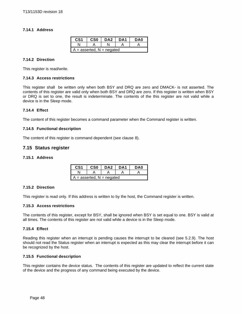
T13/1153D revision 18
Page 48
7.14.1 Address
CS1 CS0 DA2 DA1 DA0N A N A A
A = asserted, N = negated
7.14.2 Direction
This register is read/write.
7.14.3 Access restrictions
This register shall be written only when both BSY and DRQ are zero and DMACK- is not asserted. Thecontents of this register are valid only when both BSY and DRQ are zero. If this register is written when BSYor DRQ is set to one, the result is indeterminate. The contents of the this register are not valid while adevice is in the Sleep mode.
7.14.4 Effect
The content of this register becomes a command parameter when the Command register is written.
7.14.5 Functional description
The content of this register is command dependent (see clause 8).
7.15 Status register
7.15.1 Address
CS1 CS0 DA2 DA1 DA0N A A A A
A = asserted, N = negated
7.15.2 Direction
This register is read only. If this address is written to by the host, the Command register is written.
7.15.3 Access restrictions
The contents of this register, except for BSY, shall be ignored when BSY is set equal to one. BSY is valid atall times. The contents of this register are not valid while a device is in the Sleep mode.
7.15.4 Effect
Reading this register when an interrupt is pending causes the interrupt to be cleared (see 5.2.9). The hostshould not read the Status register when an interrupt is expected as this may clear the interrupt before it canbe recognized by the host.
7.15.5 Functional description
This register contains the device status. The contents of this register are updated to reflect the current stateof the device and the progress of any command being executed by the device.

T13/1153D revision 18
Page 49
7.15.6 Field/bit description
7 6 5 4 3 2 1 0BSY DRDY # # DRQ obsolete obsolete ERR
7.15.6.1 BSY (Busy)
BSY is set to one to indicate that the device is busy. After the host has written the Command register thedevice shall have either the BSY bit set to one, or the DRQ bit set to one, until command completion or thedevice has performed a bus release for an overlapped command.
The BSY bit shall be set to one by the device:1) after either the negation of RESET- or the setting of the SRST bit to one in the Device
Control register;2) after writing the Command register if the DRQ bit is not set to one;3) between blocks of a data transfer during PIO data in commands before the DRQ bit is
cleared to zero;4) after the transfer of a data block during PIO data out commands before the DRQ bit is
cleared to zero;5) during the data transfer of DMA commands either the BSY bit , the DRQ bit, or both
shall be set to one;6) after the command packet is received during the execution of a PACKET command.
NOTE − The BSY bit may be set to one and then cleared to zero so quickly, thathost detection of the BSY bit being set to one is not certain.
When BSY is set to one, the device has control of the Command Block Registers and:1) a write to a Command Block register by the host shall be ignored by the device except
for writing DEVICE RESET command;2) a read from a Command Block register by the host will most likely yield invalid contents
except for the BSY bit itself.
The BSY bit shall be cleared to zero by the device:1) after setting DRQ to one to indicate the device is ready to transfer data;2) at command completion;3) upon releasing the bus for an overlapped command;4) when the device is ready to accept commands that do not require DRDY during a
power-on, hardware or software reset.
When BSY is cleared to zero, the host has control of the Command Block registers, the deviceshall:
1) not set DRQ to one;2) not change ERR bit;3) not change the content of any other Command Block register;4) set the SERV bit to one when ready to continue an overlapped command that has been
bus released.
7.15.6.2 DRDY (Device ready)
The DRDY bit shall be cleared to zero by the device:1) when power-on, hardware, or software reset or DEVICE RESET or EXECUTE DEVICE
DIAGNOSTIC commands for devices implementing the PACKET command feature set.
When the DRDY bit is cleared to zero, the device shall accept and attempt to execute as describedin clause 8
The DRDY bit shall be set to one by the device:

T13/1153D revision 18
Page 50
1) when the device is capable of accepting all commands for devices not implementing thePACKET command feature set;
2) prior to command completion except the DEVICE RESET or EXECUTE DEVICEDIAGNOSTIC command for devices implementing the PACKET feature set.
When the DRDY bit is set to one:1) the device shall accept and attempt to execute all implemented commands;2) devices that implement the Power Management feature set shall maintain the DRDY bit
equal to one when they are in the Idle or Standby modes.
7.15.6.3 Command dependent
The use of bits marked with # are command dependent (see clause 8). Bit 4 was formerly the DSC (DeviceSeek Complete) bit.
7.15.6.4 DRQ (Data request)
DRQ indicates that the device is ready to transfer a word of data between the host and the device. After thehost has written the Command register the device shall either set the BSY bit to one or the DRQ bit to one,until command completion or the device has performed a bus release for an overlapped command.
The DRQ bit shall be set to one by the device:1) when BSY is set to one and data is ready for PIO transfer;2) during the data transfer of DMA commands either the BSY bit , the DRQ bit, or both
shall be set to one.
When the DRQ bit is set to one, the host may:1) transfer data via PIO mode;2) transfer data via DMA mode if DMARQ and DMACK- are asserted.
The DRQ bit shall be cleared to zero by the device:1) when the last word of the data transfer occurs;2) when the last word of the command packet transfer occurs for a PACKET command.
When the DRQ bit is cleared to zero, the host may:1) transfer data via DMA mode if DMARQ and DMACK- are asserted and BSY is set to
one.
7.15.6.5 Obsolete bits
Some bits in this register were defined in previous ATA standards but have been declared obsolete in thisstandard. These bits are labeled “obsolete”.
7.15.6.6 ERR (Error)
ERR indicates that an error occurred during execution of the previous command. For the PACKET andSERVICE commands, this bit is defined as CHK and indicates that an exception conditions exists.
The ERR bit shall be set to one by the device:1) when BSY or DRQ is set to one and an error occurs in the executing command.
When the ERR bit is set to one:1) the bits in the Error register shall be valid;2) the device shall not change the contents of the following registers until a new command
has been accepted, the SRST bit is set to one or RESET- is asserted:− Error register;− Cylinder High/Low registers;− Sector Count register;

T13/1153D revision 18
Page 51
− Sector Number register;− Device/Head register.
The ERR bit shall be cleared to zero by the device:1) when a new command is written to the Command register;2) when the SRST bit is set to one;3) when the RESET- signal is asserted.
When the ERR bit is cleared to zero at the end of a command:1) the content of the Error register shall be ignored by the host.
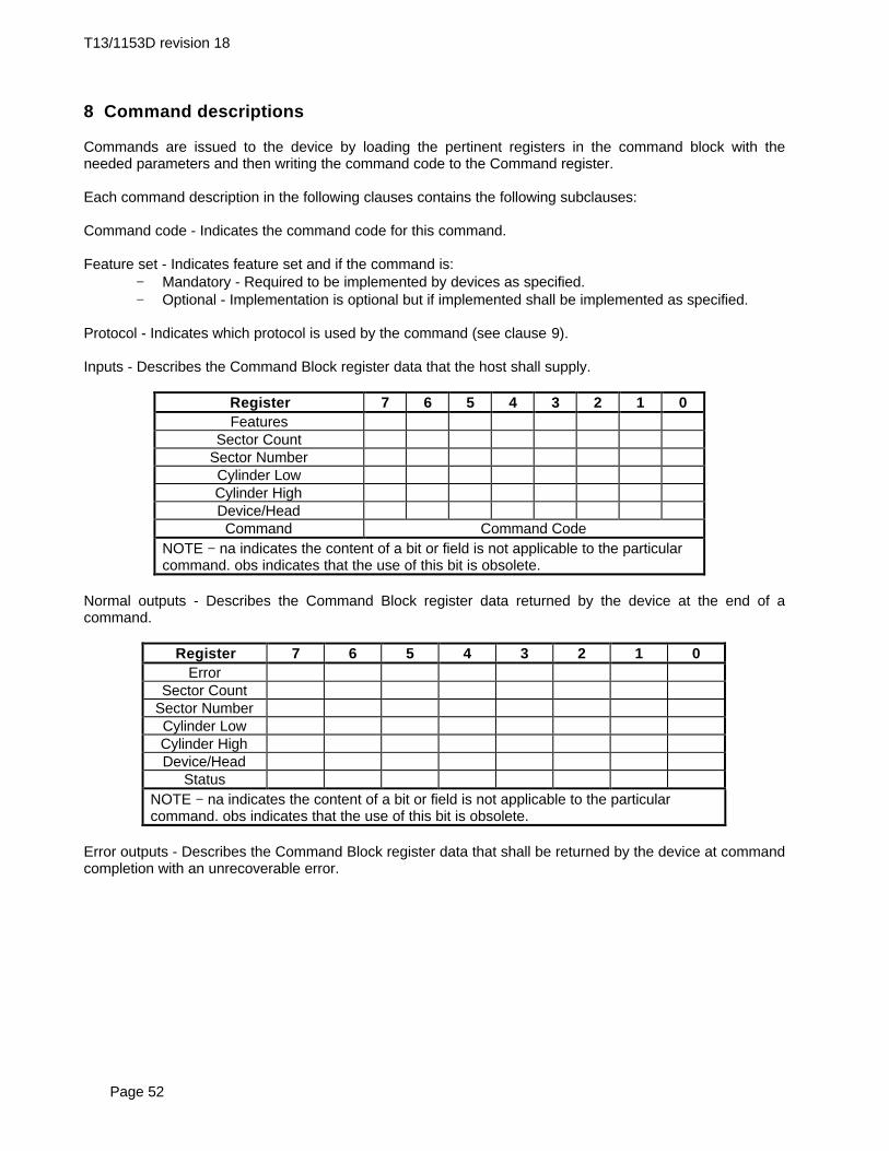
T13/1153D revision 18
Page 52
8 Command descriptions
Commands are issued to the device by loading the pertinent registers in the command block with theneeded parameters and then writing the command code to the Command register.
Each command description in the following clauses contains the following subclauses:
Command code - Indicates the command code for this command.
Feature set - Indicates feature set and if the command is:− Mandatory - Required to be implemented by devices as specified.− Optional - Implementation is optional but if implemented shall be implemented as specified.
Protocol - Indicates which protocol is used by the command (see clause 9).
Inputs - Describes the Command Block register data that the host shall supply.
Register 7 6 5 4 3 2 1 0Features
Sector CountSector NumberCylinder LowCylinder HighDevice/HeadCommand Command Code
NOTE − na indicates the content of a bit or field is not applicable to the particularcommand. obs indicates that the use of this bit is obsolete.
Normal outputs - Describes the Command Block register data returned by the device at the end of acommand.
Register 7 6 5 4 3 2 1 0Error
Sector CountSector NumberCylinder LowCylinder HighDevice/Head
StatusNOTE − na indicates the content of a bit or field is not applicable to the particularcommand. obs indicates that the use of this bit is obsolete.
Error outputs - Describes the Command Block register data that shall be returned by the device at commandcompletion with an unrecoverable error.

T13/1153D revision 18
Page 53
Register 7 6 5 4 3 2 1 0Error
Sector CountSector NumberCylinder LowCylinder HighDevice/Head
StatusNOTE − na indicates the content of a bit or field is not applicable to the particularcommand. obs indicates that the use of this bit is obsolete.
Prerequisites - Any prerequisite commands or conditions that shall be met before the command is issued.
Description - The description of the command function(s).

T13/1153D revision 18
Page 54
8.1 CFA ERASE SECTORS
8.1.1 Command code
C0h
8.1.2 Feature set
CFA feature set.− If the CFA feature set is implemented this command shall be implemented.
This command code is Vendor Specific for devices not implementing the CFA feature Set.
8.1.3 Protocol
Non-data command (see 9.9).
8.1.4 Inputs
The Cylinder Low, Cylinder High, Device/Head, and Sector Number specify the starting sector address to beerased. The Sector Count register specifies the number of sectors to be erased.
Register 7 6 5 4 3 2 1 0Features na
Sector Count Sector countSector Number Sector number or LBACylinder Low Cylinder low or LBACylinder High Cylinder high or LBADevice/Head obs LBA obs DEV Head number or LBA
Command C0h
Sector Count -number of sectors to be erased. A value of 00h indicates that 256 sectors are to be erased.
Sector Number -starting sector number or LBA address bits (7:0).
Cylinder Low -starting cylinder number bits (7:0) or LBA address bits (15:8).
Cylinder High -starting cylinder number bits (15:8) or LBA address bits (23:16).
Device/Head -bit 6 set to one if LBA address, cleared to zero if CHS address starting head number or LBA addressbits (27:24).
8.1.5 Normal outputs
Register 7 6 5 4 3 2 1 0Error na
Sector Count naSector
Numberna
Cylinder Low naCylinder High naDevice/Head obs na obs DEV na na na na
Status BSY DRDY na na na na na ERR

T13/1153D revision 18
Page 55
Status registerBSY shall be cleared to zero indicating command completion.DRDY shall be set to one.ERR shall be cleared to zero.
8.1.6 Error outputs
The device shall return command aborted if the command is not supported. An unrecoverable errorencountered during execution of this command results in the termination of the command. The commandblock registers contain the address of the sector where the first unrecovered error occurred.
Register 7 6 5 4 3 2 1 0Error na na na IDNF na ABRT na MED
Sector Count naSector
NumberSector number or LBA
Cylinder Low Cylinder low or LBACylinder High Cylinder high or LBADevice/Head obs na obs DEV Head number or LBA
Status BSY DRDY DF na na na na ERR
Error Register -IDNF shall be set to one if a user-accessible address could not be found and after an unsuccessful
INITIALIZE DEVICE PARAMETERS command until a valid CHS translation is established(see 8.16.8). IDNF shall be set to one if an address outside of the range of user-accessibleaddresses is requested if command aborted is not returned.
ABRT shall be set to one if the command is not supported. ABRT may be set to one if the device isnot able to complete the action requested by the command. ABRT shall be set to one if anaddress outside of the range of user-accessible addresses is requested if IDNF is not set toone.
MED shall be set to one if a media error is detected.Sector Number, Cylinder Low, Cylinder High, Device/Head -
shall be written with the address of first unrecoverable error.Status register -
BSY shall be cleared to zero indicating command completion.DRDY shall be set to one.DF (Device Fault) shall be set to one if a device fault has occurred.ERR shall be set to one if an Error register bit is set to one.
8.1.7 Prerequisites
DRDY set equal to one.
8.1.8 Description
This command pre-erases and conditions from 1 to 256 sectors as specified in the Sector Count register.This command should be issued in advance of a CFA WRITE SECTORS WITHOUT ERASE or a CFAWRITE MULTIPLE WITHOUT ERASE command to increase the execution speed of the write operation.
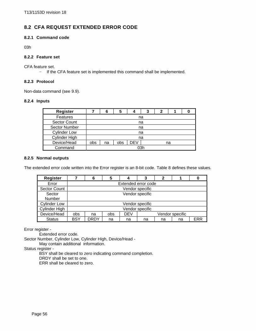
T13/1153D revision 18
Page 56
8.2 CFA REQUEST EXTENDED ERROR CODE
8.2.1 Command code
03h
8.2.2 Feature set
CFA feature set.− If the CFA feature set is implemented this command shall be implemented.
8.2.3 Protocol
Non-data command (see 9.9).
8.2.4 Inputs
Register 7 6 5 4 3 2 1 0Features na
Sector Count naSector Number naCylinder Low naCylinder High naDevice/Head obs na obs DEV na
Command 03h
8.2.5 Normal outputs
The extended error code written into the Error register is an 8-bit code. Table 8 defines these values.
Register 7 6 5 4 3 2 1 0Error Extended error code
Sector Count Vendor specificSector
NumberVendor specific
Cylinder Low Vendor specificCylinder High Vendor specificDevice/Head obs na obs DEV Vendor specific
Status BSY DRDY na na na na na ERR
Error register -Extended error code.
Sector Number, Cylinder Low, Cylinder High, Device/Head -May contain additional information.
Status register -BSY shall be cleared to zero indicating command completion.DRDY shall be set to one.ERR shall be cleared to zero.

T13/1153D revision 18
Page 57
Table 8 −− Extended error codesExtended error code Description
00h No error detected / no additional information01h Self test passed03h Write / Erase failed05h Self test or diagnostic failed09h Miscellaneous error0Bh Vendor specific0Ch Corrupted media format
0D-0Fh Vendor specific10h ID Not Found / ID Error11h Uncorrectable ECC error14h ID Not Found18h Corrected ECC error
1Dh, 1Eh Vendor specific1Fh Data transfer error / command aborted20h Invalid command21h Invalid address
22-23h Vendor specific27h Write protect violation2Fh Address overflow (address too large)
30-34h Self test or diagnostic failed35h, 36h Supply or generated voltage out of tolerance37h, 3Eh Self test or diagnostic failed
38h Corrupted media format39h Vendor specific3Ah Spare sectors exhausted
3Bh 3Ch, 3Fh Corrupted media format3Dh Vendor specific
All other values Reserved
8.2.6 Error outputs
Register 7 6 5 4 3 2 1 0Error na na na na na ABRT na na
Sector Count naSector
Numberna
Cylinder Low naCylinder High naDevice/Head obs na obs DEV na
Status BSY DRDY DF na na na na ERR
Error Register -ABRT shall be set to one if the command is not supported. ABRT may be set to one if the device isnot able to complete the action requested by the command.
Status register -BSY shall be cleared to zero indicating command completion.DRDY shall be set to one.DF (Device Fault) shall be set to one if a device fault has occurred.ERR shall be set to one if an Error register bit is set to one.

T13/1153D revision 18
Page 58
8.2.7 Prerequisites
DRDY set equal to one.
8.2.8 Description
This command provides an extended error code which identifies the cause of an error condition in moredetail than is available with Status and Error register values. The CFA REQUEST EXTENDED ERRORCODE command must be issued to the device immediately following the command which ended with anerror condition to obtain valid extended error code information.

T13/1153D revision 18
Page 59
8.3 CFA TRANSLATE SECTOR
8.3.1 Command code
87h
8.3.2 Feature set
CFA feature set.− If the CFA feature set is implemented this command shall be implemented.
This command code is Vendor Specific for devices not implementing the CFA feature Set.
8.3.3 Protocol
PIO data in command (see 9.7).
8.3.4 Inputs
Register 7 6 5 4 3 2 1 0Features na
Sector Count naSector Number Sector number or LBACylinder Low Cylinder low or LBACylinder High Cylinder high or LBADevice/Head obs LBA obs DEV Head number or LBA
Command 87h
Sector Number -sector number or LBA address bits (7:0).
Cylinder Low -cylinder number bits (7:0) or LBA address bits (15:8).
Cylinder High -cylinder number bits (15:8) or LBA address bits (23:16).
Device/Head -bit 6 set to one if LBA address, cleared to zero if CHS address head number or LBA address bits(27:24).
8.3.5 Normal outputs
A 512 byte information table is transferred to the host. Table 9 defines these values.
Register 7 6 5 4 3 2 1 0Error na
Sector Count naSector
Numberna
Cylinder Low naCylinder High naDevice/Head obs na obs DEV na
Status BSY DRDY na na na na na ERR

T13/1153D revision 18
Page 60
Status register -BSY shall be cleared to zero indicating command completion.DRDY shall be set to one.ERR shall be cleared to zero.
Table 9 −− CFA TRANSLATE SECTOR InformationByte Description00h Cylinder number MSB01h Cylinder number LSB02h Head number03h Sector number04h LBA bits (23:16)05h LBA bits (15:8)06h LBA bits (7:0)
07-12h Reserved13h Sector erased flag (FFh = erased; 00h = not erased)
14-17h Reserved18h Sector write cycles count bits (23:16)19h Sector write cycles count bits (15:8)1Ah Sector write cycles count bits (7:0)
1B-FFh Reserved
8.3.6 Error outputs
Register 7 6 5 4 3 2 1 0Error na na na na na ABRT na na
Sector Count naSector
Numberna
Cylinder Low naCylinder High naDevice/Head obs na obs DEV na
Status BSY DRDY DF na na na na ERR
Error Register -ABRT shall be set to one if the command is not supported. ABRT may be set to one if the device isnot able to complete the action requested by the command.
Status register -BSY shall be cleared to zero indicating command completion.DRDY shall be set to one.DF (Device Fault) shall be set to one if a device fault has occurred.ERR shall be set to one if an Error register bit is set to one.
8.3.7 Prerequisites
DRDY set equal to one.
8.3.8 Description
This command provides information related to a specific sector. The data indicates the erased or not erasedstatus of the sector, and the number of erase and write cycles performed on that sector. Devices may returnzero in fields that do not apply or that are not supported by the device.

T13/1153D revision 18
Page 61
8.4 CFA WRITE MULTIPLE WITHOUT ERASE
8.4.1 Command code
CDh
8.4.2 Feature set
CFA feature set.− If the CFA feature set is implemented this command shall be implemented.
8.4.3 Protocol
PIO data out command (see 9.8).
8.4.4 Inputs
The Cylinder Low, Cylinder High, Device/Head, and Sector Number specify the starting sector address to bewritten. The Sector Count register specifies the number of sectors to be transferred.
Register 7 6 5 4 3 2 1 0Features na
Sector Count Sector countSector Number Sector number or LBACylinder Low Cylinder low or LBACylinder High Cylinder high or LBADevice/Head obs LBA obs DEV Head number or LBA
Command CDh
Sector Count -number of sectors to be transferred. A value of 00h indicates that 256 sectors are to be transferred.
Sector Number -starting sector number or LBA address bits (7:0).
Cylinder Low -starting cylinder number bits (7:0) or LBA address bits (15:8).
Cylinder High -starting cylinder number bits (15:8) or LBA address bits (23:16).
Device/Head -bit 6 set to one if LBA address, cleared to zero if CHS address starting head number or LBA addressbits (27:24).
8.4.5 Normal outputs
Register 7 6 5 4 3 2 1 0Error na
Sector Count naSector
Numberna
Cylinder Low naCylinder High naDevice/Head obs na obs DEV na na na na
Status BSY DRDY na na na na na ERR
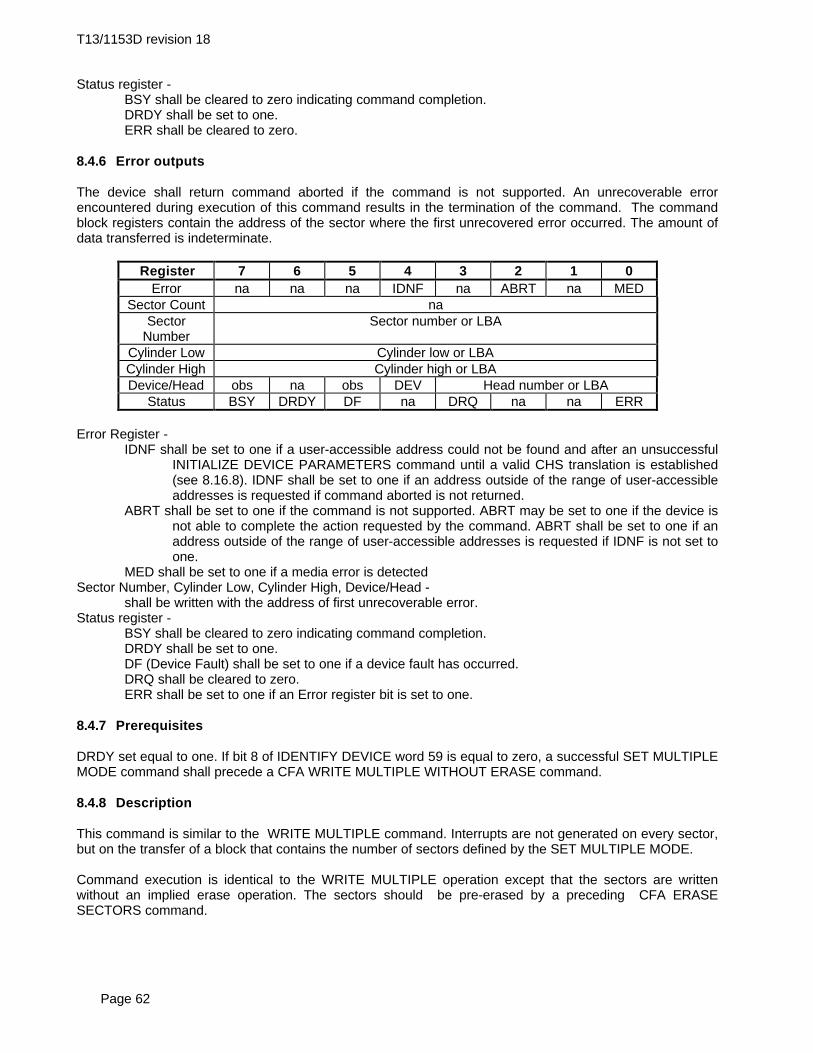
T13/1153D revision 18
Page 62
Status register -BSY shall be cleared to zero indicating command completion.DRDY shall be set to one.ERR shall be cleared to zero.
8.4.6 Error outputs
The device shall return command aborted if the command is not supported. An unrecoverable errorencountered during execution of this command results in the termination of the command. The commandblock registers contain the address of the sector where the first unrecovered error occurred. The amount ofdata transferred is indeterminate.
Register 7 6 5 4 3 2 1 0Error na na na IDNF na ABRT na MED
Sector Count naSector
NumberSector number or LBA
Cylinder Low Cylinder low or LBACylinder High Cylinder high or LBADevice/Head obs na obs DEV Head number or LBA
Status BSY DRDY DF na DRQ na na ERR
Error Register -IDNF shall be set to one if a user-accessible address could not be found and after an unsuccessful
INITIALIZE DEVICE PARAMETERS command until a valid CHS translation is established(see 8.16.8). IDNF shall be set to one if an address outside of the range of user-accessibleaddresses is requested if command aborted is not returned.
ABRT shall be set to one if the command is not supported. ABRT may be set to one if the device isnot able to complete the action requested by the command. ABRT shall be set to one if anaddress outside of the range of user-accessible addresses is requested if IDNF is not set toone.
MED shall be set to one if a media error is detectedSector Number, Cylinder Low, Cylinder High, Device/Head -
shall be written with the address of first unrecoverable error.Status register -
BSY shall be cleared to zero indicating command completion.DRDY shall be set to one.DF (Device Fault) shall be set to one if a device fault has occurred.DRQ shall be cleared to zero.ERR shall be set to one if an Error register bit is set to one.
8.4.7 Prerequisites
DRDY set equal to one. If bit 8 of IDENTIFY DEVICE word 59 is equal to zero, a successful SET MULTIPLEMODE command shall precede a CFA WRITE MULTIPLE WITHOUT ERASE command.
8.4.8 Description
This command is similar to the WRITE MULTIPLE command. Interrupts are not generated on every sector,but on the transfer of a block that contains the number of sectors defined by the SET MULTIPLE MODE.
Command execution is identical to the WRITE MULTIPLE operation except that the sectors are writtenwithout an implied erase operation. The sectors should be pre-erased by a preceding CFA ERASESECTORS command.

T13/1153D revision 18
Page 63
8.5 CFA WRITE SECTORS WITHOUT ERASE
8.5.1 Command code
38h
8.5.2 Feature set
CFA feature set.− If the CFA feature set is implemented this command shall be implemented.
8.5.3 Protocol
PIO data out command (see 9.8).
8.5.4 Inputs
The Cylinder Low, Cylinder High, Device/Head, and Sector Number specify the starting sector address to bewritten. The Sector Count register specifies the number of sectors to be transferred.
Register 7 6 5 4 3 2 1 0Features na
Sector Count Sector countSector Number Sector number or LBACylinder Low Cylinder low or LBACylinder High Cylinder high or LBADevice/Head obs LBA obs DEV Head number or LBA
Command 38h
Sector Count -number of sectors to be transferred. A value of 00h indicates that 256 sectors are to be transferred.
Sector Number -starting sector number or LBA address bits (7:0).
Cylinder Low -starting cylinder number bits (7:0) or LBA address bits (15:8).
Cylinder High -starting cylinder number bits (15:8) or LBA address bits (23:16).
Device/Head -bit 6 set to one if LBA address, cleared to zero if CHS address starting head number or LBA addressbits (27:24).
8.5.5 Normal outputs
Register 7 6 5 4 3 2 1 0Error na
Sector Count naSector
Numberna
Cylinder Low naCylinder High naDevice/Head obs na obs DEV na na na na
Status BSY DRDY na na na na na ERR

T13/1153D revision 18
Page 64
Status register -BSY shall be cleared to zero indicating command completion.DRDY shall be set to one.ERR shall be cleared to zero.
8.5.6 Error outputs
The device shall return command aborted if the command is not supported. An unrecoverable errorencountered during execution of this command results in the termination of the command. The commandblock registers contain the address of the sector where the first unrecovered error occurred. The amount ofdata transferred is indeterminate.
Register 7 6 5 4 3 2 1 0Error na na na IDNF na ABRT na MED
Sector Count naSector
NumberSector number or LBA
Cylinder Low Cylinder low or LBACylinder High Cylinder high or LBADevice/Head obs na obs DEV Head number or LBA
Status BSY DRDY DF na DRQ na na ERR
Error Register -IDNF shall be set to one if a user-accessible address could not be found and after an unsuccessful
INITIALIZE DEVICE PARAMETERS command until a valid CHS translation is established(see 8.16.8). IDNF shall be set to one if an address outside of the range of user-accessibleaddresses is requested if command aborted is not returned.
ABRT shall be set to one if the command is not supported. ABRT may be set to one if the device isnot able to complete the action requested by the command. ABRT shall be set to one if anaddress outside of the range of user-accessible addresses is requested if IDNF is not set toone.
MED shall be set to one if a media error is detectedSector Number, Cylinder Low, Cylinder High, Device/Head -
shall be written with the address of first unrecoverable error.Status register -
BSY shall be cleared to zero indicating command completion.DRDY shall be set to one.DF (Device Fault) shall be set to one if a device fault h as occurred.DRQ shall be cleared to zero.ERR shall be set to one if an Error register bit is set to one.
8.5.7 Prerequisites
DRDY set equal to one.
8.5.8 Description
This command is similar to the WRITE SECTORS command. Command execution is identical to theWRITE SECTORS operation except that the sectors are written without an implied erase operation. Thesectors should be pre-erased by a preceding CFA ERASE SECTORS command.

T13/1153D revision 18
Page 65
8.6 CHECK POWER MODE
8.6.1 Command code
E5h
8.6.2 Feature set
Power Management feature set.− Power Management feature set is mandatory when power management is not implemented by a
PACKET power management feature set.− This command is mandatory when the Power Management feature set is implemented.
8.6.3 Protocol
Non-data command (see 9.9).
8.6.4 Inputs
Register 7 6 5 4 3 2 1 0Features na
Sector Count naSector Number naCylinder Low naCylinder High naDevice/Head obs na obs DEV na na na naCommand E5h
Device/Head register -DEV shall indicate the selected device.
8.6.5 Normal outputs
Register 7 6 5 4 3 2 1 0Error na
Sector Count Result valueSector Number naCylinder Low naCylinder High naDevice/Head obs na obs DEV na na na na
Status BSY DRDY DF na DRQ na na ERR
Status register -BSY shall be cleared to zero indicating command completion.DRDY shall be set to one.DF (Device Fault) shall be cleared to zero.DRQ shall be cleared to zero.ERR shall be cleared to zero.
Device/Head register -DEV shall indicate the selected device.
T13/1153D revision 18
Page 66
Sector Count result value -00h - device is in Standby mode.80h - device is in Idle mode.FFh - device is in Active mode or Idle mode.
8.6.6 Error outputs
The device shall return command aborted if the device does not support the Power Management featureset.
Register 7 6 5 4 3 2 1 0Error na na na na na ABRT na na
Sector Count naSector Number naCylinder Low naCylinder High naDevice/Head obs na obs DEV na na na na
Status BSY DRDY DF na DRQ na na ERR
Error register -ABRT shall be set to one if Power Management feature set is not supported. ABRT may be set to one if the device is not able to complete the action requested by the command.
Device/Head register -DEV shall indicate the selected device.
Status register -BSY shall be cleared to zero indicating command completion.DRDY shall be set to one.DF (Device Fault) shall be set to one if a device fault has occurred.DRQ shall be cleared to zero.ERR shall be set to one if an Error register bit is set to one.
8.6.7 Prerequisites
DRDY set equal to one.
8.6.8 Description
The CHECK POWER MODE command allows the host to determine the current power mode of the device.The CHECK POWER MODE command shall not cause the device to change power or affect the operationof the Standby timer.

T13/1153D revision 18
Page 67
8.7 DEVICE RESET
8.7.1 Command code
08h
8.7.2 Feature set
General feature set− Use prohibited when the PACKET Command feature set is not implemented.− Mandatory when the PACKET Command feature set is implemented.
8.7.3 Protocol
Device reset (see 9.4 ).
8.7.4 Inputs
Register 7 6 5 4 3 2 1 0Features na
Sector Count naSector Number naCylinder Low naCylinder High naDevice/Head obs na obs DEV na na na naCommand 08h
Device/Head register -DEV shall indicate the selected device.
8.7.5 Normal outputs
Register 7 6 5 4 3 2 1 0Error Diagnostic results
Sector Count signatureSector Number signatureCylinder Low signatureCylinder High signatureDevice/Head 0 0 0 DEV 0 0 0 0
Status see 9.4
Error register -The diagnostic code as described in 8.9 is placed in this register.
Sector Count, Sector Number, Cylinder low, Cylinder High -Signature (see 9.1).
Device/Head register -DEV shall indicate the selected device.
Status register -see 9.4.
8.7.6 Error outputs
If supported, this command cannot end in an error condition. If this command is not supported and thedevice has the BSY bit or the DRQ bit set to one when the command is written, the results of this command

T13/1153D revision 18
Page 68
are indeterminate. If this command is not supported and the device has the BSY bit and the DRQ bit clearedto zero when the command is written, the device shall respond command aborted.
8.7.7 Prerequisites
This command shall be accepted when BSY or DRQ is set to one, DRDY is cleared to zero, or DMARQ isasserted. This command shall be accepted when in Sleep mode.
8.7.8 Description
The DEVICE RESET command enables the host to reset an individual device without affecting the otherdevice.
T13/1153D revision 18
Page 69
8.8 DOWNLOAD MICROCODE
8.8.1 Command code
92h
8.8.2 Feature set
General feature set− Optional for devices not implementing the PACKET Command feature set.− Use prohibited for devices implementing the PACKET Command feature set.
8.8.3 Protocol
PIO data out (see 9.8).
8.8.4 Inputs
The head bits of the Device/Head register shall always be cleared to zero. The Cylinder High and Lowregisters shall be cleared to zero. The Sector Number and Sector Count registers are used together as a 16-bit sector count value. The Feature register specifies the subcommand code.
Register 7 6 5 4 3 2 1 0Features Subcommand code
Sector Count Sector count (low order)Sector Number Sector count (high order)Cylinder Low 00hCylinder High 00hDevice/Head obs na obs DEV 0 0 0 0Command 92h
Device/Head register -DEV shall indicate the selected device.
8.8.5 Normal outputs
Register 7 6 5 4 3 2 1 0Error na
Sector Count naSector Number naCylinder Low naCylinder High naDevice/Head obs na obs DEV na na na na
Status BSY DRDY DF na DRQ na na ERR
Device/Head register -DEV shall indicate the selected device.
Status register -BSY shall be cleared to zero indicating command completion.DRDY shall be set to one.DF (Device Fault) shall be cleared to zero.DRQ shall be cleared to zero.ERR shall be cleared to zero.
T13/1153D revision 18
Page 70
8.8.6 Error outputs
The device shall return command aborted if the device does not support this command or did not accept themicrocode data. The device shall return command aborted if subcommand code is not a supported value.
Register 7 6 5 4 3 2 1 0Error na na na na na ABRT na na
Sector Count naSector Number naCylinder Low naCylinder High naDevice/Head obs na obs DEV na na na na
Status BSY DRDY DF na DRQ na na ERR
Error register -ABRT shall be set to one if the device does not support this command or did not accept the
microcode data. ABRT may be set to one if the device is not able to complete the actionrequested by the command.
Device/Head register -DEV shall indicate the selected device.
Status register -BSY shall be cleared to zero indicating command completion.DRDY shall be set to one.DF (Device Fault) shall be set to one if a device fault has occurred.DRQ shall be cleared to zero.ERR shall be set to one if an Error register bit is set to one.
8.8.7 Prerequisites
DRDY set equal to one.
8.8.8 Description
This command enables the host to alter the device’s microcode. The data transferred using theDOWNLOAD MICROCODE command is vendor specific.
All transfers shall be an integer multiple of the sector size. The size of the data transfer is determined bythe contents of the Sector Number Register and the Sector Count register. The Sector Number Registershall be used to extend the Sector Count register to create a sixteen bit sector count value. The SectorNumber Register shall be the most significant eight bits and the Sector Count register shall be the leastsignificant eight bits. A value of zero in both the Sector Number Register and the Sector Count registershall indicate no data is to be transferred. This allows transfer sizes from 0 bytes to 33,553,920 bytes, in512 byte increments.
The Features register shall be used to determine the effect of the DOWNLOAD MICROCODE command.The values for the Feature Register are:
− 01h - download is for immediate, temporary use.− 07h - save downloaded code for immediate and future use.
Either or both values may be supported. All other values are reserved.

T13/1153D revision 18
Page 71
8.9 EXECUTE DEVICE DIAGNOSTIC
8.9.1 Command code
90h
8.9.2 Feature set
General feature set− Mandatory for all devices.
8.9.3 Protocol
Device diagnostics (see 9.5 ).
8.9.4 Inputs
None. The device selection bit in the Device/Head register is ignored.
Register 7 6 5 4 3 2 1 0Features na
Sector Count naSector Number naCylinder Low naCylinder High naDevice/Head obs na obs na na na na naCommand 90h
Device/Head register -DEV shall indicate the selected device.
8.9.5 Normal outputs
The diagnostic code written into the Error register is an 8-bit code. Table 10 defines these values. Thevalues of the bits in the Error register are not as defined in 7.11.6.
Register 7 6 5 4 3 2 1 0Error Diagnostic code
Sector Count SignatureSector Number SignatureCylinder Low SignatureCylinder High SignatureDevice/Head Signature
Status see 9.5
Error register -Diagnostic code.
Sector Count, Sector number, Cylinder Low, Cylinder High, Device/Head registers -device signature (see 9.1).
Device/Head register -DEV shall indicate the selected device.
Status register -see 9.5.

T13/1153D revision 18
Page 72
Table 10 −− Diagnostic codesCode (see note
1)Description
When this code is in the Device 0 Error register01h Device 0 passed, Device 1 passed or not present
00h, 02h-7Fh Device 0 failed, Device 1 passed or not present81h Device 0 passed, Device 1 failed
80h, 82h-FFh Device 0 failed, Device 1 failedWhen this code is in the Device 1 Error register
01h Device 1 passed (see note 2)00h,02h-7Fh Device 1 failed (see note 2)
NOTE −1 Codes other than 01h and 81h may indicate additional informationabout the failure(s).2 If Device 1 is not present, the host may see the information fromDevice 0 even though Device 1 is selected.
8.9.6 Error outputs
Table 10 shows the error information that is returned as a diagnostic code in the Error register.
8.9.7 Prerequisites
This command shall be accepted regardless of the state of DRDY.
8.9.8 DescriptionThis command shall perform the internal diagnostic tests implemented by the device. The DEV bit in theDevice/Head register is ignored. Both devices, if present, shall execute this command regardless of whichdevice is selected.
If the host issues an EXECUTE DEVICE DIAGNOSTIC command while a device is in or going to a powermanagement mode except Sleep, then the device shall execute its EXECUTE DEVICE DIAGNOSTICsequence.

T13/1153D revision 18
Page 73
8.10 FLUSH CACHE
8.10.1 Command code
E7h
8.10.2 Feature set
General feature set− Optional for all devices.
8.10.3 Protocol
Non-data command (see 9.9).
8.10.4 Inputs
Register 7 6 5 4 3 2 1 0Features na
Sector Count naSector Number naCylinder Low naCylinder High naDevice/Head obs na obs DEV na na na naCommand E7h
Device/Head register -DEV shall indicate the selected device.
8.10.5 Normal outputs
Register 7 6 5 4 3 2 1 0Error na
Sector Count naSector Number naCylinder Low naCylinder High naDevice/Head obs na obs DEV na na na na
Status BSY DRDY DF na DRQ na na ERR
Device/Head register -DEV shall indicate the selected device.
Status register -BSY shall be cleared to zero indicating command completion.DRDY shall be set to one.DF (Device Fault) shall be cleared to zero.DRQ shall be cleared to zero.ERR shall be cleared to zero.
8.10.6 Error outputs
If the command is not supported, the device shall return command aborted. An unrecoverable errorencountered during execution of writing data results in the termination of the command and the CommandBlock registers contain the sector address of the sector where the first unrecoverable error occurred. The
T13/1153D revision 18
Page 74
sector is removed from the cache. Subsequent FLUSH CACHE commands continue the process of flushingthe cache.
Register 7 6 5 4 3 2 1 0Error na na na na na ABRT na na
Sector Count naSector Number Sector number or LBACylinder Low Cylinder low or LBACylinder High Cylinder high or LBADevice/Head obs na obs DEV Head number or LBA
Status BSY DRDY DF na DRQ na na ERR
Error register -ABRT shall be set to one if device does not support this command. ABRT may be set to one if the device is not able to complete the action requested by the command.
Sector Number, Cylinder Low, Cylinder High, Device/Head -shall be written with the address of the first unrecoverable error.
Device/Head register -DEV shall indicate the selected device.
Status register -BSY shall be cleared to zero indicating command completion.DRDY shall be set to one.DF (Device Fault) shall be set to one if a device fault has occurred.DRQ shall be cleared to zero.ERR shall be set to one if an Error register bit is set to one.
8.10.7 Prerequisites
DRDY set equal to one.
8.10.8 Description
This command is used by the host to request the device to flush the write cache. If the write cache is to beflushed, all data cached shall be written to the media. The BSY bit shall remain set to one until all data hasbeen successfully written or an error occurs. The device should use all error recovery methods available toensure the data is written successfully. The flushing of write cache may take several seconds to completedepending upon the amount of data to be flushed and the success of the operation.
NOTE − This command may take longer than 30 s to complete.

T13/1153D revision 18
Page 75
8.11 GET MEDIA STATUS
8.11.1 Command code
DAh
8.11.2 Feature set
Removable Media Status Notification feature set− Mandatory for devices implementing the Removable Media Status Notification feature set.
Removable Media feature set− Optional for devices implementing the Removable Media feature set.
8.11.3 Protocol
Non-data command (see 9.9).
8.11.4 Inputs
Register 7 6 5 4 3 2 1 0Features na
Sector Count naSector Number naCylinder Low naCylinder High naDevice/Head obs na obs DEV na na na naCommand DAh
Device/Head register -DEV shall indicate the selected device.
8.11.5 Normal outputs
Normal outputs are returned if Media Status Notification is disabled or if no bits are set to one in the Errorregister.
Register 7 6 5 4 3 2 1 0Error na
Sector Count naSector Number naCylinder Low naCylinder High naDevice/Head obs na obs DEV na na na na
Status BSY DRDY DF na DRQ na na ERR
Device/Head register -DEV shall indicate the selected device.
Status register -BSY shall be cleared to zero indicating command completion.DRDY shall be set to one.DF (Device Fault) shall be cleared to zero.DRQ shall be cleared to zero.ERR shall be cleared to zero.

T13/1153D revision 18
Page 76
8.11.6 Error outputs
If the device does not support this command, the device shall return command aborted.
Register 7 6 5 4 3 2 1 0Error na WP MC na MCR ABRT NM obs
Sector Count naSector Number naCylinder Low naCylinder High naDevice/Head obs na obs DEV na na na na
Status BSY DRDY DF na DRQ na na ERR
Error register -ABRT shall be set to one if device does not support this command. ABRT may be set to one if the
device is not able to complete the action requested by the command.NM (No Media) shall be set to one if no media is present in the device. This bit shall be set to one
for each execution of GET MEDIA STATUS until media is inserted into the device.MCR (Media Change Request) shall be set to one if the eject button is pressed by the user and
detected by the device. The device shall reset this bit after each execution of the GETMEDIA STATUS command and only set the bit again for subsequent eject button presses.
MC (Media Change) shall be set to one when the device detects media has been inserted. Thedevice shall reset this bit after each execution of the GET MEDIA STATUS command andonly set the bit again for subsequent media insertions.
WP (Write Protect) shall be set to one for each execution of GET MEDIA STATUS while the mediais write protected.
Device/Head register -DEV shall indicate the selected device.
Status register -BSY shall be cleared to zero indicating command completion.DRDY shall be set to one.DF (Device Fault) shall be set to one if a device fault has occurred.DRQ shall be cleared to zero.ERR shall be set to one if an Error register bit is set to one.
8.11.7 Prerequisites
DRDY set equal to one.
8.11.8 Description
This command returns media status bits WP, MC, MCR, and NM, as defined above. When Media StatusNotification is disabled this command returns zeros in the WP, MC, MCR, and NM bits.

T13/1153D revision 18
Page 77
8.12 IDENTIFY DEVICE
8.12.1 Command code
ECh
8.12.2 Feature set
General feature set− Mandatory for all devices.− Devices implementing the PACKET Command feature set (see 8.12.5.2).
8.12.3 Protocol
PIO data in (see 9.7).
8.12.4 Inputs
Register 7 6 5 4 3 2 1 0Features na
Sector Count naSector Number naCylinder Low naCylinder High naDevice/Head obs na obs DEV na na na naCommand ECh
Device/Head register -DEV shall indicate the selected device.
8.12.5 Outputs
8.12.5.1 Normal outputs
Register 7 6 5 4 3 2 1 0Error na
Sector Count naSector Number naCylinder Low naCylinder High naDevice/Head obs na obs DEV na na na na
Status BSY DRDY DF na DRQ na na ERR
Device/Head register -DEV shall indicate the selected device.
Status register -BSY shall be cleared to zero indicating command completion.DRDY shall be set to one.DF (Device Fault) shall be cleared to zero.DRQ shall be cleared to zero.ERR shall be cleared to zero.

T13/1153D revision 18
Page 78
8.12.5.2 Outputs for PACKET Command feature set devices
In response to this command, devices that implement the PACKET Command feature set shall postcommand aborted and place the PACKET Command feature set signature in the Command Block registers(see 9.1).
8.12.6 Error outputs
Devices not implementing the PACKET Command feature set shall not report an error.
8.12.7 Prerequisites
DRDY set equal to one.
8.12.8 Description
The IDENTIFY DEVICE command enables the host to receive parameter information from the device.
Some devices may have to read the media in order to complete this command.
When the command is issued, the device sets the BSY bit to one, prepares to transfer the 256 words ofdevice identification data to the host, sets the DRQ bit to one, clears the BSY bit to zero, and asserts INTRQif nIEN is cleared to zero. The host may then transfer the data by reading the Data register. Table 11defines the arrangement and meaning of the parameter words in the buffer. All reserved bits or words shallbe zero.
Some parameters are defined as a 16-bit value. A word that is defined as a 16-bit value places the mostsignificant bit of the value on bit DD15 and the least significant bit on bit DD0.
Some parameters are defined as 32-bit values (e.g., words 57 and 58). Such fields are transferred usingtwo successive word transfers. The device shall first transfer the least significant bits, bits 15 through 0 ofthe value, on bits DD (15:0) respectively. After the least significant bits have been transferred, the mostsignificant bits, bits 31 through 16 of the value, shall be transferred on DD (15:0) respectively.
Some parameters are defined as a string of ASCII characters. ASCII data fields shall contain only graphiccodes (i.e., code values 20h through 7Eh). For the string “Copyright”, the character “C” is the first byte, thecharacter “o” is the 2nd byte, etc. When such fields are transferred, the order of transmission is:
the 1st character (“C”) is on bits DD (15:8) of the first word, the 2nd character (“o”) is on bits DD (7:0) of the first word, the 3rd character (“p”) is on bits DD (15:8) of the second word, the 4th character (“y”) is on bits DD (7:0) of the second word, etc.
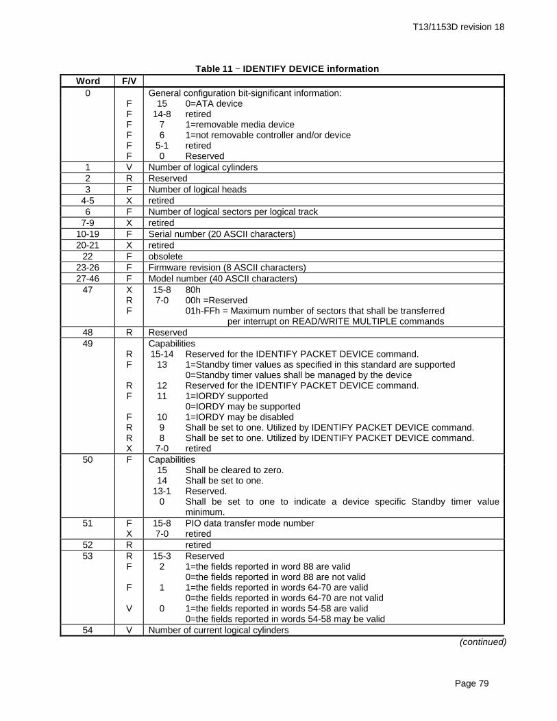
T13/1153D revision 18
Page 79
Table 11 −− IDENTIFY DEVICE informationWord F/V
0 General configuration bit-significant information:FFFFFF
1514-8
76
5-10
0=ATA deviceretired1=removable media device1=not removable controller and/or deviceretiredReserved
1 V Number of logical cylinders2 R Reserved3 F Number of logical heads
4-5 X retired6 F Number of logical sectors per logical track
7-9 X retired10-19 F Serial number (20 ASCII characters)20-21 X retired
22 F obsolete23-26 F Firmware revision (8 ASCII characters)27-46 F Model number (40 ASCII characters)
47 XRF
15-87-0
80h00h =Reserved01h-FFh = Maximum number of sectors that shall be transferred per interrupt on READ/WRITE MULTIPLE commands
48 R Reserved49 Capabilities
RF
RF
FRRX
15-1413
1211
1098
7-0
Reserved for the IDENTIFY PACKET DEVICE command.1=Standby timer values as specified in this standard are supported0=Standby timer values shall be managed by the deviceReserved for the IDENTIFY PACKET DEVICE command.1=IORDY supported0=IORDY may be supported1=IORDY may be disabledShall be set to one. Utilized by IDENTIFY PACKET DEVICE command.Shall be set to one. Utilized by IDENTIFY PACKET DEVICE command.retired
50 F Capabilities1514
13-10
Shall be cleared to zero.Shall be set to one.Reserved.Shall be set to one to indicate a device specific Standby timer valueminimum.
51 FX
15-87-0
PIO data transfer mode numberretired
52 R retired53 R
F
F
V
15-32
1
0
Reserved1=the fields reported in word 88 are valid0=the fields reported in word 88 are not valid1=the fields reported in words 64-70 are valid0=the fields reported in words 64-70 are not valid1=the fields reported in words 54-58 are valid0=the fields reported in words 54-58 may be valid
54 V Number of current logical cylinders(continued)

T13/1153D revision 18
Page 80
Table 11 −− IDENTIFY DEVICE information (continued)Word F/V
55 V Number of current logical heads56 V Number of current logical sectors per track
57-58 V Current capacity in sectors59 R
VV
15-98
7-0
Reserved1=Multiple sector setting is validxxh=Current setting for number of sectors that shall be transferred per interrupt on R/W Multiple command
60-61 F Total number of user addressable sectors (LBA mode only)62 R retired63 R
V
V
V
RFFF
15-1110
9
8
7-3210
Reserved1= Multiword DMA mode 2 is selected0= Multiword DMA mode 2 is not selected1= Multiword DMA mode 1 is selected0= Multiword DMA mode 1 is not selected1= Multiword DMA mode 0 is selected0= Multiword DMA mode 0 is not selectedReserved1= Multiword DMA mode 2 and below are supported1= Multiword DMA mode 1 and below are supported1= Multiword DMA mode 0 is supported
64 RF
15-87-0
ReservedAdvanced PIO modes supported
65 Minimum Multiword DMA transfer cycle time per wordF 15-0 Cycle time in nanoseconds
66 Manufacturer’s recommended Multiword DMA transfer cycle timeF 15-0 Cycle time in nanoseconds
67 Minimum PIO transfer cycle time without flow controlF 15-0 Cycle time in nanoseconds
68 Minimum PIO transfer cycle time with IORDY flow controlF 15-0 Cycle time in nanoseconds
69-70 R Reserved (for future command overlap and queuing)71-74 R Reserved for IDENTIFY PACKET DEVICE command.
75 F Queue depth15-54-0
ReservedMaximum queue depth
76-79 R Reserved80 F Major version number
0000h or FFFFh = device does not report version1514131211109876543210
ReservedReserved for ATA/ATAPI-14Reserved for ATA/ATAPI-13Reserved for ATA/ATAPI-12Reserved for ATA/ATAPI-11Reserved for ATA/ATAPI-10Reserved for ATA/ATAPI-9Reserved for ATA/ATAPI-8Reserved for ATA/ATAPI-7Reserved for ATA/ATAPI-6Reserved for ATA/ATAPI-51=supports ATA/ATAPI-41=supports ATA-31=supports ATA-21=supports ATA-1Reserved
(continued)

T13/1153D revision 18
Page 81
Table 11 −− IDENTIFY DEVICE information (continued)Word F/V
81 F Minor version number0000h or FFFFh=device does not report version0001h-FFFEh=see 8.12.44
82 F Command set supported. If words 82 and 83 =0000h or FFFFh command setnotification not supported.
1514131211109876543210
Obsolete1=NOP command supported1=READ BUFFER command supported1=WRITE BUFFER command supportedObsolete1=Host Protected Area feature set supported1=DEVICE RESET command supported1=SERVICE interrupt supported1=release interrupt supported1=look-ahead supported1=write cache supported1=supports PACKET Command feature set1=supports Power Management feature set1=supports Removable Media feature set1=supports Security Mode feature set1=supports SMART feature set
83 F Command sets supported. If words 82 and 83 =0000h or FFFFh command setnotification not supported.
1514
13-543210
Shall be cleared to zeroShall be set to oneReserved1=Removable Media Status Notification feature set supported1=Advanced Power Management feature set supported1=CFA feature set supported1=READ/WRITE DMA QUEUED supported1=DOWNLOAD MICROCODE command supported
84 F Command set/feature supported extension. If words 82, 83, and 84 = 0000h or FFFFhcommand set notification extension is not supported.
1514
13-0
Shall be cleared to zeroShall be set to oneReserved
85 V Command set/feature enabled. If words 85, 86, and 87 = 0000h or FFFFh commandset enabled notification is not supported.
1514131211109876543210
Obsolete1=NOP command supported1=READ BUFFER command supported1=WRITE BUFFER command supportedObsolete1=Host Protected Area feature set supported1=DEVICE RESET command supported1=SERVICE interrupt enabled1=release interrupt enabled1=look-ahead enabled1=write cache enabled1=supports PACKET Command feature set1=supports Power Management feature set1=supports Removable Media feature set1= Security Mode feature set enabled1= SMART feature set enabled
(continued)
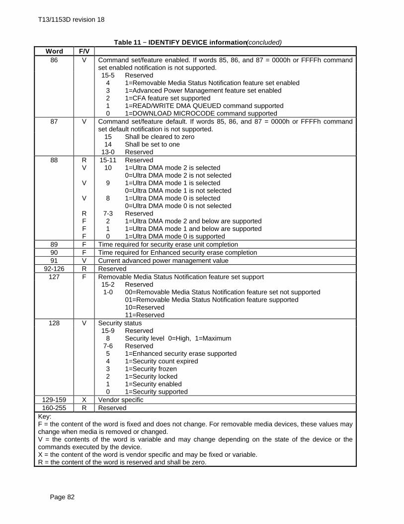
T13/1153D revision 18
Page 82
Table 11 −− IDENTIFY DEVICE information (concluded)Word F/V
86 V Command set/feature enabled. If words 85, 86, and 87 = 0000h or FFFFh commandset enabled notification is not supported.15-5
43210
Reserved1=Removable Media Status Notification feature set enabled1=Advanced Power Management feature set enabled1=CFA feature set supported1=READ/WRITE DMA QUEUED command supported1=DOWNLOAD MICROCODE command supported
87 V Command set/feature default. If words 85, 86, and 87 = 0000h or FFFFh commandset default notification is not supported.
1514
13-0
Shall be cleared to zeroShall be set to oneReserved
88 RV
V
V
RFFF
15-1110
9
8
7-3210
Reserved1=Ultra DMA mode 2 is selected0=Ultra DMA mode 2 is not selected1=Ultra DMA mode 1 is selected0=Ultra DMA mode 1 is not selected1=Ultra DMA mode 0 is selected0=Ultra DMA mode 0 is not selectedReserved1=Ultra DMA mode 2 and below are supported1=Ultra DMA mode 1 and below are supported1=Ultra DMA mode 0 is supported
89 F Time required for security erase unit completion90 F Time required for Enhanced security erase completion91 V Current advanced power management value
92-126 R Reserved127 F Removable Media Status Notification feature set support
15-21-0
Reserved00=Removable Media Status Notification feature set not supported01=Removable Media Status Notification feature supported10=Reserved11=Reserved
128 V Security status15-9
87-6543210
ReservedSecurity level 0=High, 1=MaximumReserved1=Enhanced security erase supported1=Security count expired1=Security frozen1=Security locked1=Security enabled1=Security supported
129-159 X Vendor specific160-255 R Reserved
Key:F = the content of the word is fixed and does not change. For removable media devices, these values maychange when media is removed or changed.V = the contents of the word is variable and may change depending on the state of the device or thecommands executed by the device.X = the content of the word is vendor specific and may be fixed or variable.R = the content of the word is reserved and shall be zero.
T13/1153D revision 18
Page 83
8.12.9 Word 0: General configuration
Devices that conform to this standard shall clear bit 15 to zero.
Devices reporting a value of 848Ah in this word shall support the CFA feature set.
8.12.10 Word 1: Number of cylinders
This word contains the number of user-addressable logical cylinders in the default CHS translation (see 6.2).
8.12.11 Word 2: Reserved.
8.12.12 Word 3: Number of logical heads
This word contains the number of user-addressable logical heads per logical cylinder in the default CHStranslation (see 6.2).
8.12.13 Word 4-5: Retired.
8.12.14 Word 6: Number of logical sectors per logical track
This word contains the number of user-addressable logical sectors per logical track in the default CHStranslation (see 6.2).
8.12.15 Words 7-9: Retired.
8.12.16 Words 10-19: Serial number
This field contains the serial number of the device. The contents of this field is an ASCII character string oftwenty bytes. The device shall pad the character string with spaces (20h), if necessary, to ensure that thestring is the proper length. The combination of Serial number (words 10-19) and Model number (words 27-46) shall be unique for a given manufacturer.
8.12.17 Word 20-21: Retired.
8.12.18 Word 22: Obsolete.
8.12.19 Word 23-26: Firmware revision
This field contains the firmware revision number of the device. The contents of this field is an ASCIIcharacter string of eight bytes. The device shall pad the character string with spaces (20h), if necessary, toensure that the string is the proper length.
8.12.20 Words 27-46: Model number
This field contains the model number of the device. The contents of this field is an ASCII character string offorty bytes. The device shall pad the character string with spaces (20h), if necessary, to ensure that thestring is the proper length. The combination of Serial number (words 10-19) and Model number (words 27-46) shall be unique for a given manufacturer.
8.12.21 Word 47: READ/WRITE MULTIPLE support.
Bits 7-0 of this word define the maximum number of sectors per block that the device supports forREAD/WRITE MULTIPLE commands.
8.12.22 Word 48: Reserved.
T13/1153D revision 18
Page 84
8.12.23 Word 49-50: Capabilities
Bits 15 and 14 of word 49 are reserved for use in the IDENTIFY PACKET DEVICE command response.
Bit 13 of word 49 is used to determine whether a device utilizes the Standby timer values as defined in thisstandard. Table 14 specifies the Standby timer values utilized by the device if bit 13 is set to one. If bit 13 iscleared to zero, the timer values shall be vendor specific.
Bit 12 of word 49 is reserved for use in the IDENTIFY PACKET DEVICE command response.
Bit 11 of word 49 is used to determine whether a device supports IORDY. If this bit is set to one, then thedevice supports IORDY operation. If this bit is zero, the device may support IORDY. This ensuresbackward compatibility. If a device supports PIO mode 3 or higher, then this bit shall be set to one.
Bit 10 of word 49 is used to indicate a device’s ability to enable or disable the use of IORDY. If this bit is setto one, then the device supports the disabling of IORDY. Disabling and enabling of IORDY is accomplishedusing the SET FEATURES command.
Bits 9 and 8 of word 49 shall be set to one for backward compatibility. These bits are defined for use in theIDENTIFY PACKET DEVICE command response.
Bits 7 through 0 of word 49 are retired.
Bit 15 of word 50 shall be cleared to zero to indicate that the contents of word 50 are valid.
Bit 14 of word 50 shall be set to one to indicate that the contents of word 50 are valid.
Bits 13 through 1 of word 50 are reserved.
Bit 0 of word 50 set to one indicates that the device has a minimum Standby timer value that is devicespecific.
8.12.24 Word 51: PIO data transfer mode number
The PIO transfer timing for each device falls into modes that have unique parametric timing specificationsthat are specified in 10.2.2. The value returned in Bits 15-8 shall be 00h for mode 0, 01h for mode 1, or 02hfor mode 2. Values 03h through FFh are reserved.
8.12.25 Word 52: Retired
8.12.26 Word 53: Field validity
If bit 0 of word 53 is set to one, the values reported in words 54 through 58 are valid. If this bit is cleared tozero, the values reported in words 54 through 58 may be valid. If bit 1 of word 53 is set to one, the valuesreported in words 64 through 70 are valid. If this bit is cleared to zero, the values reported in words 64-70are not valid. Any device that supports PIO mode 3 or above, or supports Multiword DMA mode 1 or above,shall set bit 1 of word 53 to one and support the fields contained in words 64 through 70. If the devicesupports Ultra DMA and the values reported in word 88 are valid, then bit 2 of word 53 shall be set to one. Ifthe device does not support Ultra DMA and the values reported in word 88 are not valid, then this bit iscleared to zero.
8.12.27 Word 54: Number of current logical cylinders
This field contains the number of user-addressable logical cylinders in the current CHS translation (see 6.2).

T13/1153D revision 18
Page 85
8.12.28 Word 55: Number of current logical heads
This field contains the number of user-addressable logical heads per logical cylinder in the current CHStranslation (see 6.2).
8.12.29 Word 56: Number of current logical sectors per logical track
This field contains the number of user-addressable logical sectors per logical track in the current CHStranslation (see 6.2).
8.12.30 Word (58:57): Current capacity in sectors
This field contains the current capacity in sectors in the current CHS translation (see 6.2).
8.12.31 Word 59: Multiple sector setting
If bit 8 is set to one, bits 7-0 reflect the number of sectors currently set to transfer on a READ/WRITEMULTIPLE command. If word 47 bits 7-0 are zero then word 59 bits 8-0 shall also be zero. This field maydefault to the preferred value for the device.
8.12.32 Word (61:60): Total number of user addressable sectors
This field contains the total number of user addressable sectors (see 6.2).
8.12.33 Word 62: Retired
8.12.34 Word 63: Multiword DMA transfer
Word 63 indentifies the Multiword DMA transfer modes supported by the device and indicates the mode thatis currently selected.
8.12.34.1 Reserved
Bits 15 though 11 of word 63 are reserved.
8.12.34.2 Multiword DMA mode 2 selected
If bit 10 of word 63 is set to one, then Multiword DMA mode 2 is selected. If this bit is cleared to zero, thenMultiword DMA mode 2 is not selected. If bit 9 is set to one or if bit 8 is set to one, then this bit shall becleared to zero.
8.12.34.3 Multiword DMA mode 1 selected
If bit 9 of word 63 is set to one, then Multiword DMA mode 1 is selected. If this bit is cleared to zero thenMultiword DMA mode 1 is not selected. If bit 10 is set to one or if bit 8 is set to one, then this bit shall becleared to zero.
8.12.34.4 Multiword DMA mode 0 selected
If bit 8 of word 63 is set to one, then Multiword DMA mode 0 is selected. If this bit is cleared to zero thenMultiword DMA mode 0 is not selected. If bit 10 is set to one or if bit 9 is set to one, then this bit shall becleared to zero.
8.12.34.5 Reserved
Bits 7 through 3 of word 63 are reserved.

T13/1153D revision 18
Page 86
8.12.34.6 Multiword DMA mode 2 supported
If bit 2 of word 63 is set to one, then Multiword DMA modes 2 and below are supported. If this bit is clearedto zero, then Multiword DMA mode 2 is not supported. If Multiword DMA mode 2 is supported, thenMultiword DMA modes 1 and 0 shall also be supported. If this bit is set to one, bits 1 and 0 shall be set toone.
8.12.34.7 Multiword DMA mode 1 supported
If bit 1 of word 63 is set to one, then Multiword DMA modes 1 and below are supported. If this bit is clearedto zero, then Multiword DMA mode 1 is not supported. If Multiword DMA mode 1 is supported, thenMultiword DMA mode 0 shall also be supported. If this bit is set to one, bit 0 shall be set to one.
8.12.34.8 Multiword DMA mode 0 supported
If bit 0 of word 63 is set to one, then Multiword DMA mode 0 is supported.
8.12.35 Word 64: PIO transfer modes supported
Bits 7 through 0 of word 64 of the Identify Device parameter information is defined as the advanced PIOdata transfer supported field. If this field is supported, bit 1 of word 53 shall be set to one. This field is bitsignificant. Any number of bits may be set to one in this field by the device to indicate the advanced PIOmodes it is capable of supporting.
Of these bits, bits 7 through 2 are Reserved for future advanced PIO modes. Bit 0, if set to one, indicatesthat the device supports PIO mode 3. Bit 1, if set to one, indicates that the device supports PIO mode 4.
8.12.36 Word 65: Minimum Multiword DMA transfer cycle time per word
Word 65 of the parameter information of the IDENTIFY DEVICE command is defined as the minimumMultiword DMA transfer cycle time per word. This field defines, in nanoseconds, the minimum cycle timethat the device supports when performing Multiword DMA transfers on a per word basis.
If this field is supported, bit 1 of word 53 shall be set to one. Any device that supports Multiword DMA mode1 or above shall support this field, and the value in word 65 shall not be less than the minimum cycle timefor the fastest DMA mode supported by the device.
If bit 1 of word 53 is set to one because a device supports a field in words 64-70 other than this field and thedevice does not support this field, the device shall return a value of zero in this field.
8.12.37 Word 66: Device recommended Multiword DMA cycle time
Word 66 of the parameter information of the IDENTIFY DEVICE command is defined as the devicerecommended Multiword DMA transfer cycle time. This field defines, in nanoseconds, the minimum cycletime per word during a single sector host transfer while performing a multiple sector READ DMA or WRITEDMA command for any location on the media under nominal conditions. If a host runs at a faster cycle rateby operating at a cycle time of less than this value, the device may negate DMARQ for flow control. Therate at which DMARQ is negated could result in reduced throughput despite the faster cycle rate. Transferat this rate does not ensure that flow control will not be used, but implies that higher performance mayresult.
If this field is supported, bit 1 of word 53 shall be set to one. Any device that supports Multiword DMA mode1 or above shall support this field, and the value in word 66 shall not be less than the value in word 65.
If bit 1 of word 53 is set to one because a device supports a field in words 64-70 other than this field and thedevice does not support this field, the device shall return a value of zero in this field.

T13/1153D revision 18
Page 87
8.12.38 Word 67: Minimum PIO transfer cycle time without flow control
Word 67 of the parameter information of the IDENTIFY DEVICE command is defined as the minimum PIOtransfer without flow control cycle time. This field defines, in nanoseconds, the minimum cycle time that, ifused by the host, the device guarantees data integrity during the transfer without utilization of flow control.
If this field is supported, Bit 1 of word 53 shall be set to one.
Any device that supports PIO mode 3 or above shall support this field, and the value in word 67 shall not beless than the value reported in word 68.
If bit 1 of word 53 is set to one because a device supports a field in words 64-70 other than this field and thedevice does not support this field, the device shall return a value of zero in this field.
8.12.39 Word 68: Minimum PIO transfer cycle time with IORDY
Word 68 of the parameter information of the IDENTIFY DEVICE command is defined as the minimum PIOtransfer with IORDY flow control cycle time. This field defines, in nanoseconds, the minimum cycle timethat the device supports while performing data transfers while utilizing IORDY flow control.
If this field is supported, Bit 1 of word 53 shall be set to one.
Any device that supports PIO mode 3 or above shall support this field, and the value in word 68 shall be thefastest defined PIO mode supported by the device.
If bit 1 of word 53 is set to one because a device supports a field in words 64-70 other than this field and thedevice does not support this field, the device shall return a value of zero in this field.
8.12.40 Words 69-74: Reserved
8.12.41 Word 75: Queue depth
Bits 4 through 0 of word 75 indicate the maximum queue depth supported by the device. If bit 1 of word 83is cleared to zero indicating that the device does not support READ/WRITE DMA QUEUED commands, thevalue in this field shall be 00h. If bit 1 of word 83 is set to one, bits 4 through 0 indicate the maximum queuedepth supported. A device may support READ/WRITE DMA QUEUED commands to provide overlap only(i.e., queuing not supported), in this case, bit 1 of word 83 shall be set to one and the queue depth shall beset to 00h.
8.12.42 Words 76-79: Reserved
8.12.43 Word 80: Major version number
If not 0000h or FFFFh, the device claims compliance with the major version(s) as indicated by bits 1 through4 being equal to one. Values other than 0000h and FFFFh are bit significant. Since ATA standards maintaindownward compatibility, it is allowed for a device to set more than one bit.
8.12.44 Word 81: Minor version number
If an implementor claims that the revision of the standard they used to guide their implementation does notneed to be reported or if the implementation was based upon a standard prior to the ATA-3 standard, word81 shall be 0000h or FFFFh.
Table 12 defines the value that may optionally be reported in word 81 to indicate the revision of the standardthat guided the implementation.

T13/1153D revision 18
Page 88
Table 12 −− Minor version numberValue Minor revision0001h ATA (ATA-1) X3T9.2 781D prior to revision 40002h ATA-1 published, ANSI X3.221-19940003h ATA (ATA-1) X3T10 781D revision 40004h ATA-2 published, ANSI X3.279-19960005h ATA-2 X3T10 948D prior to revision 2k0006h ATA-3 X3T10 2008D revision 10007h ATA-2 X3T10 948D revision 2k0008h ATA-3 X3T10 2008D revision 00009h ATA-2 X3T10 948D revision 3000Ah ATA-3 published, ANSI X3.298-199x000Bh ATA-3 X3T10 2008D revision 6000Ch ATA-3 X3T13 2008D revision 7 and 7a000Dh ATA/ATAPI-4 X3T13 1153D revision 6000Eh ATA/ATAPI-4 T13 1153D revision 13000Fh ATA/ATAPI-4 X3T13 1153D revision 70010h Reserved0011h ATA/ATAPI-4 T13 1153D revision 15
0012h-0013h Reserved0014h ATA/ATAPI-4 T13 1153D revision 14
0015h-0016h Reserved0017h ATA/ATAPI-4 T13 1153D revision 17
0018h-FFFFh Reserved
8.12.45 Words 82-84: Features/command sets supported
Words 82, 83, and 84 shall indicate features/command sets supported. The value 0000h or FFFFh wasplaced in each of these words by devices prior to ATA-3 and shall be interpreted by the host as meaningthat features/command sets supported are not indicated. Bits 1 through 13 of word 83 and bits 0 through 13of word 84 are reserved. Bit 14 of word 83 and word 84 shall be set to one and bit 15 of word 83 and word84 shall be cleared to zero to provide indication that the features/command sets supported words are valid.
If bit 0 of word 82 is set to one, the SMART feature set is supported.
If bit 1 of word 82 is set to one, the Security Mode feature set is supported.
If bit 2 of word 82 is set to one, the Removable Media feature set is supported.
If bit 3 of word 82 is set to one, the Power Management feature set is supported.
If bit 4 of word 82 is set to one, the PACKET Command feature set is supported.
If bit 5 of word 82 is set to one, write cache is supported.
If bit 6 of word 82 is set to one, look-ahead is supported.
If bit 7 of word 82 is set to one, release interrupt is supported.
If bit 8 of word 82 is set to one, SERVICE interrupt is supported.
If bit 9 of word 82 is set to one, the DEVICE RESET command is supported.
If bit 10 of word 82 is set to one, the Host Protected Area feature set is supported.
Bit 11 of word 82 is obsolete.

T13/1153D revision 18
Page 89
If bit 12 of word 82 is set to one, the device supports the WRITE BUFFER command.
If bit 13 of word 82 is set to one, the device supports the READ BUFFER command.
If bit 14 of word 82 is set to one, the device supports the NOP command.
Bit 15 of word 82 is obsolete.
If bit 0 of word 83 is set to one, the device supports the DOWNLOAD MICROCODE command.
If bit 1 of word 83 is set to one, the device supports the READ DMA QUEUED and WRITE DMA QUEUEDcommands.
If bit 2 of word 83 is set to one, the device supports the CFA feature set.
If bit 3 of word 83 is set to one, the device supports the Advanced Power Management feature set.
If bit 4 of word 83 is set to one, the device supports the Removable Media Status feature set.
8.12.46 Words 85-87: Features/command sets enabled
Words 85, 86, and 87 shall indicate features/command sets enabled. The value 0000h or FFFFh was placedin each of these words by devices prior to ATA-4 and shall be interpreted by the host as meaning thatfeatures/command sets enabled are not indicated. Bits 1 through 15 of word 86 are reserved. Bits 0-13 ofword 87 are reserved. Bit 14 of word 87 shall be set to one and bit 15 of word 87 shall be cleared to zero toprovide indication that the features/command sets enabled words are valid.
If bit 0 of word 85 is set to one, the SMART feature set has been enabled via the SMART ENABLEOPERATIONS command.
If bit 1 of word 85 is set to one, the Security Mode feature set has been enabled via the SECURITY SETPASSWORD command.
If bit 2 of word 85 is set to one, the Removable Media feature set is supported.
If bit 3 of word 85 is set to one, the Power Management feature set is supported.
If bit 4 of word 85 is set to one, the PACKET Command feature set is supported.
If bit 5 of word 85 is set to one, write cache has been enabled via the SET FEATURES command (see8.37.9).
If bit 6 of word 85 is set to one, look-ahead has been enabled via the SET FEATURES command (see8.37.13).
If bit 7 of word 85 is set to one, release interrupt has been enabled via the SET FEATURES command (see8.37.14).
If bit 8 of word 85 is set to one, SERVICE interrupt has been enabled via the SET FEATURES command(see 8.37.15).
If bit 9 of word 85 is set to one, the DEVICE RESET command is supported.
If bit 10 of word 85 is set to one, the Host Protected Area feature set is supported.
Bit 11 of word 85 is obsolete.

T13/1153D revision 18
Page 90
If bit 12 of word 85 is set to one, the device supports the WRITE BUFFER command.
If bit 13 of word 85 is set to one, the device supports the READ BUFFER command.
If bit 14 of word 85 is set to one, the device supports the NOP command.
Bit 15 of word 85 is obsolete.
If bit 0 of word 86 is set to one, the device supports the DOWNLOAD MICROCODE command.
If bit 1 of word 86 is set to one, the device supports the READ DMA QUEUED and WRITE DMA QUEUEDcommands.
If bit 2 of word 86 is set to one, the device supports the CFA feature set.
If bit 3 of word 86 is set to one, the Advanced Power Management feature set has been enabled via theSET FEATURES command.
If bit 4 of word 86 is set to one, the Removable Media Status feature set has been enabled via the SETFEATURES command.
8.12.47 Word 88: Ultra DMA modes
Only one Ultra DMA mode shall be selected at any time. If an Ultra DMA mode is enabled, no MultiwordDMA mode shall be enabled. If a Multiword DMA mode is enabled, no Ultra DMA mode shall be enabled.
8.12.47.1 Reserved
Bits 15 though 11 of word 88 are reserved.
8.12.47.2 Ultra DMA mode 2 selected
If bit 10 of word 88 is set to one, then Ultra DMA mode 2 is selected. If this bit is cleared to zero, then UltraDMA mode 2 is not selected. If bit 9 is set to one or if bit 8 is set to one, then this bit shall be cleared tozero.
8.12.47.3 Ultra DMA mode 1 selected
If bit 9 of word 88 is set to one, then Ultra DMA mode 1 is selected. If this bit is cleared to zero then UltraDMA mode 1 is not selected. If bit 10 is set to one or if bit 8 is set to one, then this bit shall be cleared tozero.
8.12.47.4 Ultra DMA mode 0 selected
If bit 8 of word 88 is set to one, then Ultra DMA mode 0 is selected. If this bit is cleared to zero then UltraDMA mode 0 is not selected. If bit 10 is set to one or if bit 9 is set to one, then this bit shall be cleared tozero.
8.12.47.5 Reserved
Bits 7 through 3 of word 88 are reserved.
8.12.47.6 Ultra DMA mode 2 supported
If bit 2 of word 88 is set to one, then Ultra DMA modes 2 and below are supported. If this bit is cleared tozero, then Ultra DMA mode 2 is not supported. If Ultra DMA mode 2 is supported, then Ultra DMA modes 1and 0 shall also be supported. If this bit is set to one, bits 1 and 0 shall be set to one.
T13/1153D revision 18
Page 91
8.12.47.7 Ultra DMA mode 1 supported
If bit 1 of word 88 is set to one, then Ultra DMA modes 1 and below are supported. If this bit is cleared tozero, then Ultra DMA mode 1 is not supported. If Ultra DMA mode 1 is supported, then Ultra DMA mode 0shall also be supported. If this bit is set to one, bit 0 shall be set to one.
8.12.47.8 Ultra DMA mode 0 supported
If bit 0 of word 88 is set to one, then Ultra DMA mode 0 is supported. If this bit is cleared to zero, then UltraDMA is not supported.
8.12.48 Word 89: Time required for Security erase unit completion
Word 89 specifies the time required for the SECURITY ERASE UNIT command to complete.
Value Time0 Value not specified
1-254 (Value*2) minutes255 >508 minutes
8.12.49 Word 90: Time required for Enhanced security erase unit completion
Word 90 specifies the time required for the ENHANCED SECURITY ERASE UNIT command to complete.
Value Time0 Value not specified
1-254 (Value*2) minutes255 >508 minutes
8.12.50 Word 91: Advanced power management level value
Bits 7-0 of word 91 contain the current Advanced Power Management level setting.
8.12.51 Words 92-126: Reserved
8.12.52 Word 127: Removable Media Status Notification feature set support
If bit 0 of word 127 is set to one and bit 1 of word 127 is cleared to zero, the device supports the RemovableMedia Status Notification feature set. Bits 15 through 2 shall be cleared to zero.
8.12.53 Word 128: Security status
Bit 8 of word 128 indicates the security level. If security mode is enabled and the security level is high, bit 8shall be cleared to zero. If security mode is enabled and the security level is maximum, bit 8 shall be set toone. When security mode is disabled, bit 8 shall be cleared to zero.
Bit 5 of word 128 indicates the Enhanced security erase unit feature is supported. If bit 5 is set to one, theEnhanced security erase unit feature set is supported.
Bit 4 of word 128 indicates that the security count has expired. If bit 4 is set to one, the security count isexpired and SECURITY UNLOCK and SECURITY ERASE UNIT are command aborted until a power-onreset or hard reset.
Bit 3 of word 128 indicates security Frozen. If bit 3 is set to one, the security is Frozen.
Bit 2 of word 128 indicates security locked. If bit 2 is set to one, the security is locked.

T13/1153D revision 18
Page 92
Bit 1 of word 128 indicates security enabled. If bit 1 is set to one, the security is enabled.
Bit 0 of word 128 indicates the Security Mode feature set supported. If bit 0 is set to one, security issupported.
8.12.54 Words 129-159: Vendor specific.
8.12.55 Words 160-255: Reserved.
T13/1153D revision 18
Page 93
8.13 IDENTIFY PACKET DEVICE
8.13.1 Command code
A1h
8.13.2 Feature set
PACKET Command feature set− Use prohibited for devices not implementing the PACKET Command feature set.− Mandatory for devices implementing the PACKET Command feature set.
8.13.3 Protocol
PIO data in (see 9.7).
8.13.4 Inputs
Register 7 6 5 4 3 2 1 0Features na
Sector Count naSector Number naCylinder Low naCylinder High naDevice/Head obs na obs DEV na na na naCommand A1h
Device/Head register -DEV shall indicate the selected device.
8.13.5 Normal outputs
Register 7 6 5 4 3 2 1 0Error na
Sector Count naSector Number naCylinder Low naCylinder High naDevice/Head obs na obs DEV na na na na
Status BSY DRDY DF na DRQ na na ERR
Device/Head register -DEV shall indicate the selected device.
Status register -BSY shall be cleared to zero indicating command completion.DRDY shall be set to one.DF (Device Fault) shall be cleared to zero.DRQ shall be cleared to zero.ERR shall be cleared to zero.
8.13.6 Error outputs
The device shall return command aborted if the device does not implement this command, otherwise, thedevice shall not report an error.

T13/1153D revision 18
Page 94
8.13.7 Prerequisites
This command shall be accepted regardless of the state of DRDY.
8.13.8 Description
The IDENTIFY PACKET DEVICE command enables the host to receive parameter information from adevice that implements the PACKET Command feature set.
Some devices may have to read the media in order to complete this command.
When the command is issued, the device sets the BSY bit to one, prepares to transfer the 256 words ofdevice identification data to the host, sets the DRQ bit to one, clears the BSY bit to zero, and asserts INTRQif nIEN is cleared to zero. The host may then transfer the data by reading the Data register. Table 13defines the arrangement and meanings of the parameter words in the buffer. All reserved bits or words shallbe zero.
Some parameters are defined as a group of bits. A word that is defined as a set of bits is transmitted withindicated bits on the respective data bus bit (e.g., bit 15 appears on DD15).
Some parameters are defined as a 16-bit value. A word that is defined as a 16-bit value places the mostsignificant bit of the value on bit DD15 and the least significant bit on bit DD0.
Some parameters are defined as 32-bit values (e.g., words 57 and 58). Such fields are transferred usingtwo word transfers. The device shall first transfer the least significant bits, bits 15 through 0 of the value, onbits DD (15:0) respectively. After the least significant bits have been transferred, the most significant bits,bits 31 through 16 of the value, shall be transferred on DD (15:0) respectively.
Some parameters are defined as a string of ASCII characters. For the string “Copyright”, the character “C” isthe first byte, the character “o” is the 2nd byte, etc. When such fields are transferred, the order oftransmission is:
the 1st character (“C”) is on bits DD (15:8) of the first word, the 2nd character (“o”) is on bits DD (7:0) of the first word, the 3rd character (“p”) is on bits DD (15:8) of the second word, the 4th character (“y”) is on bits DD (7:0) of the second word, etc.

T13/1153D revision 18
Page 95
Table 13 −− IDENTIFY PACKET DEVICE information (continued)Word F/V
0 General configuration bit-significant information:F
RFFF
RF
15-14
1312-8
76-5
4-21-0
10=ATAPI device11=reservedreservedField indicates command packet set used by device1=removable media device00=Device shall set DRQ to one within 3 ms of receiving PACKETcommand.01=Device shall assert INTRQ when DRQ is set to one after receivingPACKET.10=Device shall set DRQ to one within 50 µs of receiving PACKETcommand.11=reservedreserved00=12 byte command packet01=16 byte command packet1x=reserved
1-9 R Reserved10-19 F Serial number (20 ASCII characters)20-22 R Reserved23-26 F Firmware revision (8 ASCII characters)27-46 F Model number (40 ASCII characters)47-48 R Reserved
49 CapabilitiesFFFFFFFFX
15141312111098
7-0
1=interleaved DMA supported1=command queuing supported1=overlap operation supported1=ATA software reset required (obsolete)1=IORDY supported1=IORDY may be disabled1=LBA supported1=DMA supportedVendor specific
50 R Reserved51 F
X15-87-0
PIO data transfer mode numberVendor specific
52 R Reserved53 R
F
F
V
15-32
1
0
Reserved1=the fields reported in word 88 are valid0=the fields reported in word 88 are not valid1=the fields reported in words 64-70 are valid0=the fields reported in words 64-70 are not valid1=the fields reported in words 54-58 are valid0=the fields reported in words 54-58 may be valid
54-62 R Reserved(continued)

T13/1153D revision 18
Page 96
Table 13 −− IDENTIFY PACKET DEVICE information(continued)Word F/V
63 RV
V
V
RFFF
15-1110
9
8
7-3210
Reserved1= Multiword DMA mode 2 is selected0= Multiword DMA mode 2 is not selected1= Multiword DMA mode 1 is selected0= Multiword DMA mode 1 is not selected1= Multiword DMA mode 0 is selected0= Multiword DMA mode 0 is not selectedReserved1= Multiword DMA mode 2 and below are supported1= Multiword DMA mode 1 and below are supported1= Multiword DMA mode 0 is supported Multiword DMA mode selected
64 RF
15-87-0
ReservedAdvanced PIO transfer modes supported
65 Minimum Multiword DMA transfer cycle time per wordF 15-0 Cycle time in nanoseconds
66 Manufacturer’s recommended Multiword DMA transfer cycle timeF 15-0 Cycle time in nanoseconds
67 Minimum PIO transfer cycle time without flow controlF 15-0 Cycle time in nanoseconds
68 Minimum PIO transfer cycle time with IORDY flow controlF 15-0 Cycle time in nanoseconds
69-70 R Reserved (for future command overlap and queuing)71 F Typical time in ns from receipt of PACKET command to bus release.72 F Typical time in ns from receipt of SERVICE command to BSY cleared to zero
73-74 R Reserved75 F Queue depth
15-54-0
ReservedMaximum queue depth supported
76-79 R Reserved80 F Major version number
0000h or FFFFh = device does not report version1514131211109876543210
ReservedReserved for ATA/ATAPI-14Reserved for ATA/ATAPI-13Reserved for ATA/ATAPI-12Reserved for ATA/ATAPI-11Reserved for ATA/ATAPI-10Reserved for ATA/ATAPI-9Reserved for ATA/ATAPI-8Reserved for ATA/ATAPI-7Reserved for ATA/ATAPI-6Reserved for ATA/ATAPI-51=supports ATA/ATAPI-41=supports ATA-31=supports ATA-21=supports ATA-1Reserved
81 F Minor version number0000h or FFFFh=device does not report version0001h-FFFEh=see 8.12.44
(continued)

T13/1153D revision 18
Page 97
Table 13 −− IDENTIFY PACKET DEVICE information (continued)Word F/V
82 F Command set supported. If words 82 and 83 =0000h or FFFFh command setnotification not supported.
1514131211109876543210
Obsolete1=NOP command supported1=READ BUFFER command supported1=WRITE BUFFER command supportedObsolete1=Host Protected Area feature set supported1=DEVICE RESET command supported1=SERVICE interrupt supported1=release interrupt supported1=look-ahead supported1=write cache supported1=supports PACKET Command feature set1=supports Power Management feature set1=supports Removable Media feature set1=supports Security Mode feature set1=supports SMART feature set
83 F Command sets supported. If words 82 and 83 =0000h or FFFFh command setnotification not supported.
1514
13-54
3-10
Shall be cleared to zeroShall be set to oneReserved1=Removable Media Status Notification feature set supportedReserved1=DOWNLOAD MICROCODE command supported
84 F Command set/feature supported extension. If words 82, 83, and 84 = 0000h or FFFFhcommand set notification extension is not supported.
1514
13-0
Shall be cleared to zeroShall be set to oneReserved
85 V Command set/feature enabled. If words 85, 86, and 87 = 0000h or FFFFh commandset enabled notification is not supported.
1514131211109876543210
Obsolete1=NOP command supported1=READ BUFFER command supported1=WRITE BUFFER command supportedObsolete1=Host Protected Area feature set supported1=DEVICE RESET command supported1=SERVICE interrupt enabled1=release interrupt enabled1=look-ahead enabled1=write cache enabled1=supports PACKET Command feature set1=supports Power Management feature set1=supports Removable Media feature set1= Security Mode feature set enabled1= SMART feature set enabled
(continued)

T13/1153D revision 18
Page 98
Table 13 −− IDENTIFY PACKET DEVICE information (concluded)Word F/V
86 V Command set/feature enabled. If words 85, 86, and 87 = 0000h or FFFFh commandset enabled notification is not supported.15-5
4
3-10
Reserved1=Removable Media Status Notification feature set enabled via the SETFEATURES command.Reserved1=DOWNLOAD MICROCODE command supported
87 V Command set/feature default. If words 85, 86, and 87 = 0000h or FFFFh commandset default notification is not supported.
1514
13-0
Shall be cleared to zeroShall be set to oneReserved
88 RV
V
V
RFFF
15-1110
9
8
7-3210
Reserved1=Ultra DMA mode 2 is selected0=Ultra DMA mode 2 is not selected1=Ultra DMA mode 1 is selected0=Ultra DMA mode 1 is not selected1=Ultra DMA mode 0 is selected0=Ultra DMA mode 0 is not selectedReserved1=Ultra DMA mode 2 and below are supported1=Ultra DMA mode 1 and below are supported1=Ultra DMA mode 0 is supported
89-126 R Reserved127 F Removable Media Status Notification feature set support
15-21-0
Reserved00=Removable Media Status Notification feature set not supported01=Removable Media Status Notification feature set supported10=Reserved11=Reserved
128 V Security status15-9
87-6543210
ReservedSecurity level 0=High, 1=MaximumReserved1=Enhanced security erase supported1=Security count expired1=Security frozen1=Security locked1=Security enabled1=Security supported
129-159 X Vendor specific160-255 R Reserved
Key:F = the content of the word is fixed and does not change. For removable media devices, these values maychange when media is removed or changed.V = the contents of the word is variable and may change depending on the state of the device or thecommands executed by the device.X = the content of the word is vendor specific and may be fixed or variable.R = the content of the word is reserved and shall be zero.
T13/1153D revision 18
Page 99
8.13.9 Word 0: General configuration
Bits 15 and 14 of word 0 indicate the type of device. If bit 15 is cleared to zero the device does notimplement the PACKET Command feature set. If bit 15 is set to one and bit 14 is cleared to zero, the deviceimplements the PACKET Command feature set. The value bit 15 and bit 14 both set to one is reserved.
Bits 12 through 8 of word 0 indicate the command packet set implemented by the device. This value followsthe peripheral device type value as defined in X3T10/995D, SCSI-3 Primary Commands.
Value Description00h Direct-access device01h Sequential-access device02h Printer device03h Processor device04h Write-once device05h CD-ROM device06h Scanner device07h Optical memory device08h Medium changer device09h Communications device
0A-0Bh Reserved for ACS IT80Ch Array controller device
0D-1Eh Reserved1Fh Unknown or no device type
Bit 7 if set to one indicates that the device has removable media.
Bits 6 and 5 of word 0 indicates the DRQ response time when a PACKET command is received. A value of00b indicates a maximum time of 3 ms from receipt of PACKET to the setting of DRQ to one. A value of01b indicates that INTRQ shall be asserted when DRQ is set to one and that this action will occur within 10ms of the receipt of PACKET. A value of 10b indicates a maximum time of 50 µs from the receipt ofPACKET to the setting of DRQ to one. The value 11b is reserved.
Bits 1 and 0 of word 0 indicate the packet size the device supports. A value of 00b indicates that a 12 bytepacket is supported; a value of 01b indicates a 16 byte packet. The values 10b and 11b are reserved.
8.13.10 Words 1-9: Reserved
8.13.11 Words 10-19: Serial numberThe use of these words is optional. If not implemented, the content shall be zeros. If implemented, thecontent shall be as described in words 10-19 of the IDENTIFY DEVICE command (see 8.12.16).
8.13.12 Words 20-22: Reserved
8.13.13 Words 23-26: Firmware revision
Words 23 through 26 shall have the content described for words 23 through 26 of the IDENTIFY DEVICEcommand.
8.13.14 Words 27-46: Model number
Words 27 through 46 shall have the content described for words 27 through 46 of the IDENTIFY DEVICEcommand.
8.13.15 Words 47-48: Reserved

T13/1153D revision 18
Page 100
8.13.16 Word 49: Capabilities
Bit 15 of word 49 is used to indicated that the device supports interleaved DMA data transfer for overlappedDMA commands.
Bit 14 of word 49 is used to indicated that the device supports command queuing for overlapped commands.If bit 14 is set to one, bit 13 shall be set to one.
Bit 13 of word 49 is used to indicated that the device supports command overlap operation.
Bit 12 of word 49 indicates that the device requires a software reset to reset the device when BSY is set toone. Some devices produced before this standard are unable to process a DEVICE RESET when the BSYbit is set to one. The use of this bit is obsolete.
Bit 11 of word 49 is used to determine whether a device supports IORDY. If this bit is set to one, then thedevice supports IORDY operation. If this bit is zero, the device may support IORDY. This ensuresbackward compatibility. If a device supports PIO mode 3 or higher, then this bit shall be set to one.
Bit 10 of word 49 is used to indicate a device’s ability to enable or disable the use of IORDY. If this bit is setto one, then the device supports the disabling of IORDY. Disabling and enabling of IORDY is accomplishedusing the SET FEATURES command.
Bit 9 of word 49 indicates that an LBA translation is supported
Bits 8 of word 49 indicates that DMA is supported.
8.13.17 Word 50: Reserved
8.13.18 Word 51: PIO data transfer mode number
Word 51 shall have the content described for word 51 of the IDENTIFY DEVICE command.
8.13.19 Word 52: Reserved
8.13.20 Word 53: Field validity
Word 53 shall have the content described for word 53 of the IDENTIFY DEVICE command.
8.13.21 Words 54-62: Reserved
8.13.22 Word 63: Multiword DMA transfer
Word 63 shall have the content described for word 63 of the IDENTIFY DEVICE command.
8.13.23 Word 64: PIO transfer mode supported
Word 64 shall have the content described for word 64 of the IDENTIFY DEVICE command.
8.13.24 Word 65: Minimum multiword DMA transfer cycle time per word
Word 65 shall have the content described for word 65 of the IDENTIFY DEVICE command.
8.13.25 Word 66: Device recommended multiword DMA cycle time
Word 66 shall have the content described for word 66 of the IDENTIFY DEVICE command.
8.13.26 Word 67: Minimum PIO transfer cycle time without flow control

T13/1153D revision 18
Page 101
Word 67 shall have the content described for word 67 of the IDENTIFY DEVICE command.
8.13.27 Word 68: Minimum PIO transfer cycle time with IORDY
Word 68 shall have the content described for word 68 of the IDENTIFY DEVICE command.
8.13.28 Word 69-70: Reserved
8.13.29 Word 71: PACKET to bus release time
Word 71 shall contain the typical time (99.7 % of the time) in microseconds from the receipt of a PACKETcommand until the device performs a bus release.
8.13.30 Word 72: SERVICE to bus release time
Word 72 shall contain the typical time (the mean plus three standard deviations) in microseconds from thereceipt of a SERVICE command until the device performs a bus release.
8.13.31 Word 73-74: Reserved
8.13.32 Word 75: Queue depth
Bits 4 through 0 of word 75 shall have the content described for word 75 of the IDENTIFY DEVICEcommand.
8.13.33 Words 76-79: Reserved
8.13.34 Word 80: Major revision number
Word 80 shall have the content described for word 80 of the IDENTIFY DEVICE command.
8.13.35 Word 81: Minor revision number
Word 81 shall have the content described for word 81 of the IDENTIFY DEVICE command.
8.13.36 Words 82-84: Features/command sets supported
Words 82, 83, and 84 shall have the content described for words 82, 83, and 84 of the IDENTIFY DEVICEcommand.
8.13.37 Words 85-87: Features/command sets enabled
Words 85, 86, and 87 shall have the content described for words 85, 86, and 87 of the IDENTIFY DEVICEcommand.
8.13.38 Word 88:Ultra DMA modes
Word 88 shall have the content described for word 88 of the IDENTIFY DEVICE command.
8.13.39 Word 89: Time required for Security erase unit completion
Word 89 shall have the content described for word 89 of the IDENTIFY DEVICE command.
8.13.40 Word 90: Time required for Enhanced security erase unit completion
Word 90 shall have the content described for word 90 of the IDENTIFY DEVICE command.

T13/1153D revision 18
Page 102
8.13.41 Word 127: Removable Media Status Notification feature set support
Word 127 shall have the content described for word 127 of the IDENTIFY DEVICE command.
8.13.42 Word 128: Security status
Word 128 shall have the content described for word 128 of the IDENTIFY DEVICE command.
8.13.43 Words 129-255: Reserved

T13/1153D revision 18
Page 103
8.14 IDLE
8.14.1 Command code
E3h
8.14.2 Feature set
Power Management feature set.− Power Management feature set is mandatory when power management is not implemented by a
PACKET power management feature set.− This command is mandatory when the Power Management feature set is implemented.
8.14.3 Protocol
Non-data command (see 9.9).
8.14.4 Inputs
Values other than zero in the Sector Count register when the IDLE command is issued shall determine thetime period programmed into the Standby timer. Table 14 defines these values.
Register 7 6 5 4 3 2 1 0Features na
Sector Count Timer period valueSector Number naCylinder Low naCylinder High naDevice/Head obs na obs DEV na na na naCommand E3h
Device/Head register -DEV shall indicate the selected device.
Table 14 −− Automatic Standby timer periodsSector Count register
contentsCorresponding timeout period
0 (00h) Timeout disabled1-240 (01h-F0h) (value * 5) s
241-251 (F1h-FBh) ((value - 240) * 30) min252 (FCh) 21 min253 (FDh) Period between 8 and 12 hrs254 (FEh) Reserved255 (FFh) 21 min 15 s
NOTE − Times are approximate.

T13/1153D revision 18
Page 104
8.14.5 Normal outputs
Register 7 6 5 4 3 2 1 0Error na
Sector Count naSector Number naCylinder Low naCylinder High naDevice/Head obs na obs DEV na na na na
Status BSY DRDY DF na DRQ na na ERR
Device/Head register -DEV shall indicate the selected device.
Status register -BSY shall be cleared to zero indicating command completion.DRDY shall be set to one.DF (Device Fault) shall be cleared to zero.DRQ shall be cleared to zero.ERR shall be cleared to zero.
8.14.6 Error outputs
The device shall return command aborted if the device does not support the Power Management featureset.
Register 7 6 5 4 3 2 1 0Error na na na na na ABRT na na
Sector Count naSector Number naCylinder Low naCylinder High naDevice/Head obs na obs DEV na na na na
Status BSY DRDY DF na DRQ na na ERR
Error register -ABRT shall be set to one if Power Management feature set is not supported. ABRT may be set to one if the device is not able to complete the action requested by the command.
Device/Head register -DEV shall indicate the selected device.
Status register -BSY shall be cleared to zero indicating command completion.DRDY shall be set to one.DF (Device Fault) shall be set to one if a device fault has occurred.DRQ shall be cleared to zero.ERR shall be set to one if an Error register bit is set to one.
8.14.7 Prerequisites
DRDY set equal to one.
8.14.8 Description
The IDLE command allows the host to place the device in the Idle mode using the Standby timer. INTRQmay be asserted even though the device may not have fully transitioned to Idle mode.

T13/1153D revision 18
Page 105
If the Sector Count register is non-zero then the Standby timer shall be enabled. The value in the SectorCount register shall be used to determine the time programmed into the Standby timer (see 6.8). If theSector Count register is zero then the Standby timer is disabled.

T13/1153D revision 18
Page 106
8.15 IDLE IMMEDIATE
8.15.1 Command code
E1h
8.15.2 Feature set
Power Management feature set.− Power Management feature set is mandatory when power management is not implemented by a
PACKET power management feature set.− This command is mandatory when the Power Management feature set is implemented.
8.15.3 Protocol
Non-data command (see 9.9).
8.15.4 Inputs
Register 7 6 5 4 3 2 1 0Features na
Sector Count naSector Number naCylinder Low naCylinder High naDevice/Head obs na obs DEV na na na naCommand E1h
Device/Head register -DEV shall indicate the selected device.
8.15.5 Normal outputs
Register 7 6 5 4 3 2 1 0Error na
Sector Count naSector Number naCylinder Low naCylinder High naDevice/Head obs na obs DEV na na na na
Status BSY DRDY DF na DRQ na na ERR
Device/Head register -DEV shall indicate the selected device.
Status register -BSY shall be cleared to zero indicating command completion.DRDY shall be set to one.DF (Device Fault) shall be cleared to zero.DRQ shall be cleared to zero.ERR shall be cleared to zero.

T13/1153D revision 18
Page 107
8.15.6 Error outputs
The device shall return command aborted if the device does not support the Power Management featureset.
Register 7 6 5 4 3 2 1 0Error na na na na na ABRT na na
Sector Count naSector Number naCylinder Low naCylinder High naDevice/Head obs na obs DEV na na na na
Status BSY DRDY DF na DRQ na na ERR
Error register -ABRT shall be set to one if Power Management feature set is not supported. ABRT may be set to one if the device is not able to complete the action requested by the command.
Device/Head register -DEV shall indicate the selected device.
Status register -BSY shall be cleared to zero indicating command completion.DRDY shall be set to one.DF (Device Fault) shall be set to one if a device fault has occurred.DRQ shall be cleared to zero.ERR shall be set to one if an Error register bit is set to one.
8.15.7 Prerequisites
DRDY set equal to one.
8.15.8 Description
The IDLE IMMEDIATE command allows the host to immediately place the device in the Idle mode. INTRQmay be asserted even though the device may not have fully transitioned to Idle mode (see 6.8).
T13/1153D revision 18
Page 108
8.16 INITIALIZE DEVICE PARAMETERS
8.16.1 Command code
91h
8.16.2 Feature set
General feature set− Mandatory for devices not implementing the PACKET Command feature set if a CHS
translation is supported.− Not mandatory for devices not implementing the PACKET command feature set if the device
capacity is greater then 8 Gbytes and only LBA translation is supported.− Use prohibited for devices implementing the PACKET Command feature set.
8.16.3 Protocol
Non-data (see 9.9).
8.16.4 Inputs
The Sector Count register specifies the number of logical sectors per logical track, and the Device/Headregister specifies the maximum head number.
Register 7 6 5 4 3 2 1 0Features na
Sector Count Logical sectors per logical trackSector Number naCylinder Low naCylinder High naDevice/Head obs na obs DEV Max headCommand 91h
Device/Head register -DEV shall indicate the selected device.
8.16.5 Normal outputs
Register 7 6 5 4 3 2 1 0Error na
Sector Count naSector Number naCylinder Low naCylinder High naDevice/Head obs na obs DEV na na na na
Status BSY na DF na DRQ na na ERR
Device/Head register -DEV shall indicate the selected device.
Status register -BSY shall be cleared to zero indicating command completion.DF (Device Fault) shall be cleared to zero.DRQ shall be cleared to zero.ERR shall be cleared to zero.

T13/1153D revision 18
Page 109
8.16.6 Error outputs
Register 7 6 5 4 3 2 1 0Error na na na na na ABRT na na
Sector Count naSector Number naCylinder Low naCylinder High naDevice/Head obs na obs DEV na na na na
Status BSY na DF na DRQ na na ERR
Error register -ABRT shall be set to one if the device does not support the requested CHS translation. ABRT maybe set to one if the device is not able to complete the action requested by the command.
Device/Head register -DEV shall indicate the selected device.
Status register -BSY shall be cleared to zero indicating command completion.DF (Device Fault) shall be set to one if a device fault has occurred.DRQ shall be cleared to zero.ERR shall be set to one if an Error register bit is set to one.
8.16.7 Prerequisites
This command shall be accepted regardless of the state of DRDY.
8.16.8 Description
This command enables the host to set the number of logical sectors per track and the number of logicalheads minus 1, per logical cylinder for the current CHS translation mode.
If the capacity of the device is less than 16,514,064 sectors, a device shall support the CHS translationdescribed in words 1, 3, and 6 of the IDENTIFY DEVICE information. Support of other CHS translations isoptional.
If the host requests a CHS translation that is not supported by the device, the device shall return commandaborted. The device shall also clear bit 0 of word 53 in the IDENTIFY DEVICE data to zero, and the contentof words 54, 55, 56, and (58:57) may be zero until a supported translation is requested by the host.
If the requested CHS translation is not supported, the device shall fail all media access commands with anID Not Found error until a valid CHS translation is established.
After a successful INITIALIZE DEVICE PARAMETERS command the content of all IDENTIFY DEVICEwords shall comply with 6.2.1 in addition to the following:1) The content of words 1, 3, 6, and (61:60) shall be unchanged.2) The content of word 55 shall equal the (Max head value requested by the host + 1).3) The content of word 56 shall equal the (Logical sectors per logical track value requested by the host).4) If the content of word (61:60) is less than or equal to 16,514,064, then word 54 shall equal the whole
number result of [[(the content of words (61:60)) ÷ [(the new content of word 55 as determined by thesuccessful INITIALIZE DEVICE PARAMETERS command) * (the new content of word 56 as determinedby the successful INITIALIZE DEVICE PARAMETERS command)]], or 65,535 whichever is less.
5) If the content of word (61:60) is greater than 16,514,064, then word 54 shall equal the whole numberresult of [[(16,514,064) ÷ [(the new content of word 55 as determined by the successful INITIALIZEDEVICE PARAMETERS command) * (the new content of word 56 as determined by the successfulINITIALIZE DEVICE PARAMETERS command)]] or 65,535 whichever is less.

T13/1153D revision 18
Page 110
6) Words (58:57) shall equal [(the new content of word 54) * (the new content of word 55) * (the newcontent of word 56)].

T13/1153D revision 18
Page 111
8.17 MEDIA EJECT
8.17.1 Command code
EDh
8.17.2 Feature set
Removable Media Status Notification feature set− Mandatory for devices not implementing the PACKET command feature set and implementing
the Removable Media Status Notification feature set.− Prohibited for devices implementing the PACKET command feature set.
Removable Media feature set− Mandatory for devices not implementing the PACKET command feature set and implementing
the Removable Media feature set.− Prohibited for devices implementing the PACKET command feature set.
8.17.3 Protocol
Non-data command (see 9.9).
8.17.4 Inputs
Register 7 6 5 4 3 2 1 0Features na
Sector Count naSector Number naCylinder Low naCylinder High naDevice/Head obs na obs DEV na na na naCommand EDh
Device/Head register -DEV shall indicate the selected device.
8.17.5 Normal outputs
Register 7 6 5 4 3 2 1 0Error na
Sector Count naSector Number naCylinder Low naCylinder High naDevice/Head obs na obs DEV na na na na
Status BSY DRDY DF na DRQ na na ERR
Device/Head register -DEV shall indicate the selected device.
Status register -BSY shall be cleared to zero indicating command completion.DRDY shall be set to one.DF (Device Fault) shall be cleared to zero.DRQ shall be cleared to zero.ERR shall be cleared to zero.

T13/1153D revision 18
Page 112
8.17.6 Error outputs
If the device does not support this command, the device shall return command aborted.
Register 7 6 5 4 3 2 1 0Error na na na na na ABRT NM obs
Sector Count naSector Number naCylinder Low naCylinder High naDevice/Head obs na obs DEV na na na na
Status BSY DRDY DF na DRQ na na ERR
Error register -ABRT shall be set to one if device does not support this command. ABRT may be set to one if the
device is not able to complete the action requested by the command.NM (No Media) shall be set to one if no media is present in the device.
Device/Head register -DEV shall indicate the selected device.
Status register -BSY shall be cleared to zero indicating command completion.DRDY shall be set to one.DF (Device Fault) shall be set to one if a device fault has occurred.DRQ shall be cleared to zero.ERR shall be set to one if an Error register bit is set to one.
8.17.7 Prerequisites
DRDY set equal to one.
8.17.8 Description
This command causes any pending operations to complete, spins down the device if needed, unlocks themedia if locked, and ejects the media. The device keeps track of only one level of media lock.

T13/1153D revision 18
Page 113
8.18 MEDIA LOCK
8.18.1 Command code
DEh
8.18.2 Feature set
Removable Media Status Notification feature set− Optional for devices not implementing the PACKET command feature set and implementing the
Removable Media Status Notification feature set.− Prohibited for device implementing the PACKET command feature set.
Removable Media feature set− Mandatory for devices not implementing the PACKET command feature set and implementing
the Removable Media feature set.− Prohibited for devices implementing the PACKET command feature set.
8.18.3 Protocol
Non-data command (see 9.9).
8.18.4 Inputs
Register 7 6 5 4 3 2 1 0Features na
Sector Count naSector Number naCylinder Low naCylinder High naDevice/Head obs na obs DEV na na na naCommand DEh
Device/Head register -DEV shall indicate the selected device.
8.18.5 Normal outputs
Register 7 6 5 4 3 2 1 0Error na
Sector Count naSector Number naCylinder Low naCylinder High naDevice/Head obs na obs DEV na na na na
Status BSY DRDY DF na DRQ na na ERR
Device/Head register -DEV shall indicate the selected device.
Status register -BSY shall be cleared to zero indicating command completion.DRDY shall be set to one.DF (Device Fault) shall be cleared to zero.DRQ shall be cleared to zero.ERR shall be cleared to zero.

T13/1153D revision 18
Page 114
8.18.6 Error outputs
If the device does not support this command, the device shall return command aborted.
Register 7 6 5 4 3 2 1 0Error na na na na MCR ABRT NM obs
Sector Count naSector Number naCylinder Low naCylinder High naDevice/Head obs na obs DEV na na na na
Status BSY DRDY DF na DRQ na na ERR
Error register -ABRT shall be set to one if device does not support this command. ABRT may be set to one if the
device is not able to complete the action requested by the command.NM (No Media) shall be set to one if no media is present in the device.MCR (Media Change Request) shall be set to one if the device is locked and a media change
request has been detected by the device.Device/Head register -
DEV shall indicate the selected device.Status register -
BSY shall be cleared to zero indicating command completion.DRDY shall be set to one.DF (Device Fault) shall be set to one if a device fault has occurred.DRQ shall be cleared to zero.ERR shall be set to one if an Error register bit is set to one.
8.18.7 Prerequisites
DRDY set equal to one.
8.18.8 Description
This command can be used to lock the media, if Media Status Notification is disabled. If Media StatusNotification is enabled, this command will return good status (no ERR bit in the Status register) and performno action.
If the media is unlocked and media is present, the media shall be set to the LOCKED state and no Errorregister bit shall be set to one. The device keeps track of only one level of media lock. Subsequent MEDIALOCK commands, while the media is in the LOCKED state, do not set additional levels of media locks.
If the media is locked, the status returned shall indicate whether a media change request has been detectedby the device. If a media change request has been detected, the MCR bit in the Error register and the ERRbit in the Status register shall be set to one.
When media is in the LOCKED state, the device shall respond to the media change request button, bysetting the MCR bit in the Error register and the ERR bit in the Status register to one, until the mediaLOCKED condition is cleared.
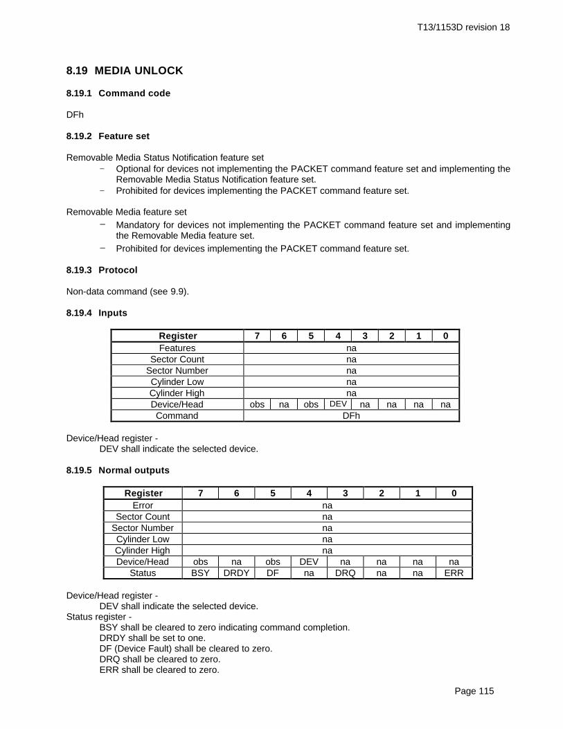
T13/1153D revision 18
Page 115
8.19 MEDIA UNLOCK
8.19.1 Command code
DFh
8.19.2 Feature set
Removable Media Status Notification feature set− Optional for devices not implementing the PACKET command feature set and implementing the
Removable Media Status Notification feature set.− Prohibited for devices implementing the PACKET command feature set.
Removable Media feature set− Mandatory for devices not implementing the PACKET command feature set and implementing
the Removable Media feature set.− Prohibited for devices implementing the PACKET command feature set.
8.19.3 Protocol
Non-data command (see 9.9).
8.19.4 Inputs
Register 7 6 5 4 3 2 1 0Features na
Sector Count naSector Number naCylinder Low naCylinder High naDevice/Head obs na obs DEV na na na naCommand DFh
Device/Head register -DEV shall indicate the selected device.
8.19.5 Normal outputs
Register 7 6 5 4 3 2 1 0Error na
Sector Count naSector Number naCylinder Low naCylinder High naDevice/Head obs na obs DEV na na na na
Status BSY DRDY DF na DRQ na na ERR
Device/Head register -DEV shall indicate the selected device.
Status register -BSY shall be cleared to zero indicating command completion.DRDY shall be set to one.DF (Device Fault) shall be cleared to zero.DRQ shall be cleared to zero.ERR shall be cleared to zero.
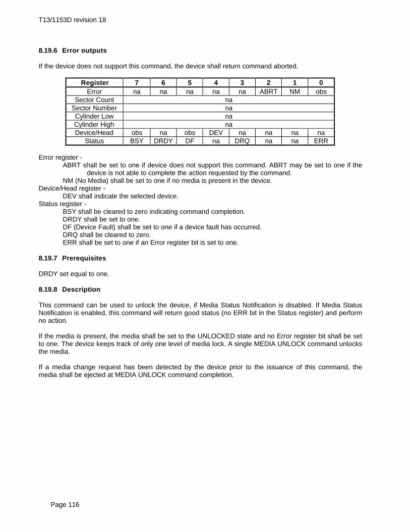
T13/1153D revision 18
Page 116
8.19.6 Error outputs
If the device does not support this command, the device shall return command aborted.
Register 7 6 5 4 3 2 1 0Error na na na na na ABRT NM obs
Sector Count naSector Number naCylinder Low naCylinder High naDevice/Head obs na obs DEV na na na na
Status BSY DRDY DF na DRQ na na ERR
Error register -ABRT shall be set to one if device does not support this command. ABRT may be set to one if the
device is not able to complete the action requested by the command.NM (No Media) shall be set to one if no media is present in the device.
Device/Head register -DEV shall indicate the selected device.
Status register -BSY shall be cleared to zero indicating command completion.DRDY shall be set to one.DF (Device Fault) shall be set to one if a device fault has occurred.DRQ shall be cleared to zero.ERR shall be set to one if an Error register bit is set to one.
8.19.7 Prerequisites
DRDY set equal to one.
8.19.8 Description
This command can be used to unlock the device, if Media Status Notification is disabled. If Media StatusNotification is enabled, this command will return good status (no ERR bit in the Status register) and performno action.
If the media is present, the media shall be set to the UNLOCKED state and no Error register bit shall be setto one. The device keeps track of only one level of media lock. A single MEDIA UNLOCK command unlocksthe media.
If a media change request has been detected by the device prior to the issuance of this command, themedia shall be ejected at MEDIA UNLOCK command completion.

T13/1153D revision 18
Page 117
8.20 NOP
8.20.1 Command code
00h
8.20.2 Feature set
General feature set− Optional for devices not implementing the PACKET Command feature set.− Mandatory for devices implementing the PACKET Command feature set.− Mandatory for devices implementing the Overlapped feature set.
8.20.3 Protocol
Non-data (see 9.9).
8.20.4 Inputs
Register 7 6 5 4 3 2 1 0Features Subcommand code
Sector Count naSector Number naCylinder Low naCylinder High naDevice/Head obs na obs DEV na na na naCommand 00h
Features register -
Subcommand code Description Action00h NOP Return command aborted and abort any
outstanding queue.01h NOP Auto Poll Return command aborted and do not abort any
outstanding queue.02h-FFh Reserved Return command aborted and do not abort any
outstanding queue.
Device/Head register -DEV shall indicate the selected device.
8.20.5 Normal outputs
This command always fails with an error.
8.20.6 Error outputs
The Command Block registers, other than the Error and Status registers, are not changed by this command.This command always fails with the device returning command aborted.
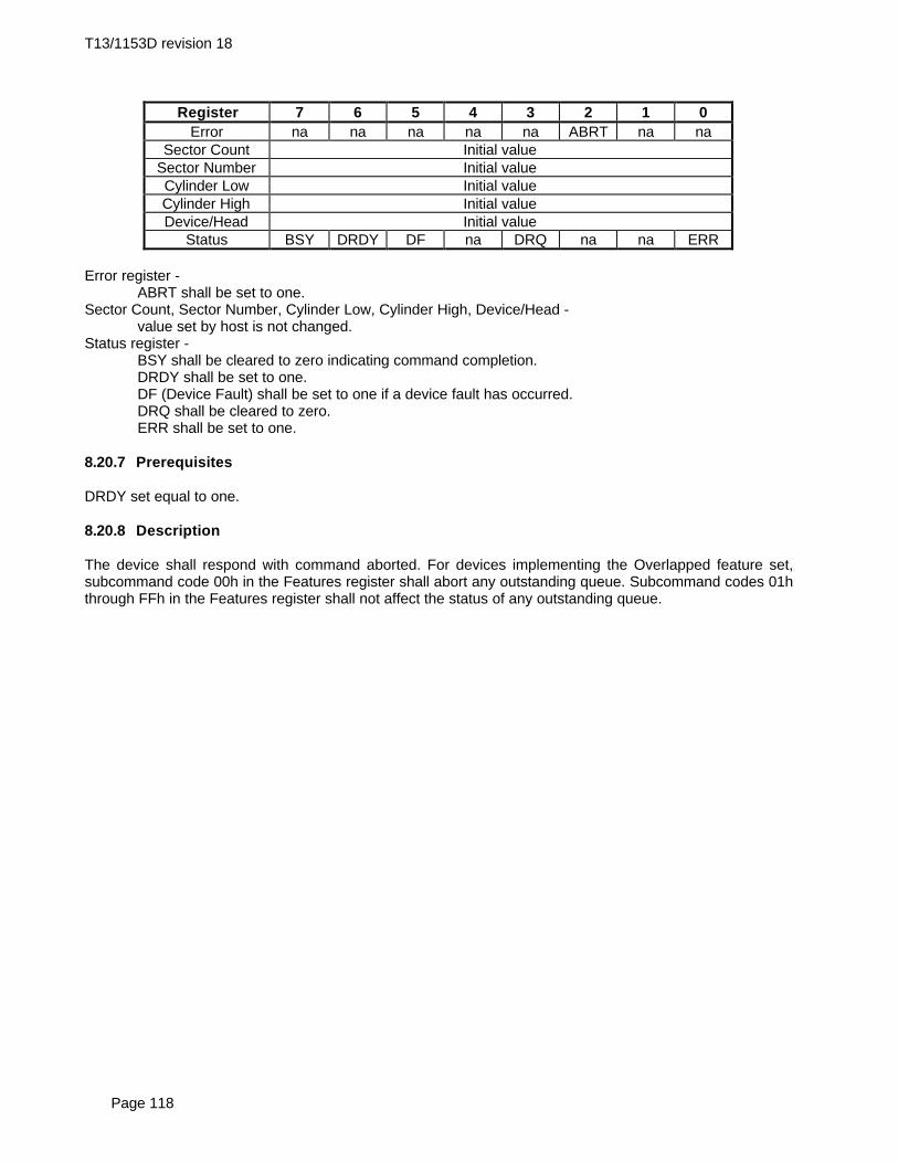
T13/1153D revision 18
Page 118
Register 7 6 5 4 3 2 1 0Error na na na na na ABRT na na
Sector Count Initial valueSector Number Initial valueCylinder Low Initial valueCylinder High Initial valueDevice/Head Initial value
Status BSY DRDY DF na DRQ na na ERR
Error register -ABRT shall be set to one.
Sector Count, Sector Number, Cylinder Low, Cylinder High, Device/Head -value set by host is not changed.
Status register -BSY shall be cleared to zero indicating command completion.DRDY shall be set to one.DF (Device Fault) shall be set to one if a device fault has occurred.DRQ shall be cleared to zero.ERR shall be set to one.
8.20.7 Prerequisites
DRDY set equal to one.
8.20.8 Description
The device shall respond with command aborted. For devices implementing the Overlapped feature set,subcommand code 00h in the Features register shall abort any outstanding queue. Subcommand codes 01hthrough FFh in the Features register shall not affect the status of any outstanding queue.

T13/1153D revision 18
Page 119
8.21 PACKET
8.21.1 Command code
A0h
8.21.2 Feature set
PACKET Command feature set− Use prohibited for devices not implementing the PACKET Command feature set.− Mandatory for devices implementing the PACKET Command feature set.
8.21.3 Protocol
Packet (see 9.11).
8.21.4 Inputs
Register 7 6 5 4 3 2 1 0Features na na na na na na OVL DMA
Sector Count Tag naSector Number naByte count low(Cylinder Low)
Byte count limit (7-0)
Byte count high(Cylinder High)
Byte count limit (15-8)
Device/Head obs na obs DEV na na na naCommand A0h
Features register -OVL - This bit is set to one to inform the device that the PACKET command is to be overlapped.DMA - This bit is set to one to inform the device that the data transfer (not the command packet
transfer) associated with this command is via DMA or Ultra DMA mode.Sector Count register -
Tag - If the device supports command queuing, this field contains the command Tag for thecommand being delivered. If queuing is not supported, this field is not applicable.
Byte count low and Byte count high registers -These registers are written by the host with the maximum byte count that is to be transferred in anysingle DRQ assertion for PIO transfers. The byte count does not apply to the command PACKETtransfer. If the PACKET command does not transfer data, the byte count is ignored.
If the PACKET command results in a data transfer:1) the host shall not set the byte count limit to zero. If the host sets the byte count limit to zero
the device shall return command aborted;2) the value set into the byte count limit shall be even if the total requested data transfer length
is greater than the byte count limit;3) the value set into the byte count limit may be odd if the total requested data transfer length
is equal to or less than the byte count limit;4) the value FFFFh is interpreted by the device as though it were FFFEh.
Device/Head register -DEV shall indicate the selected device.
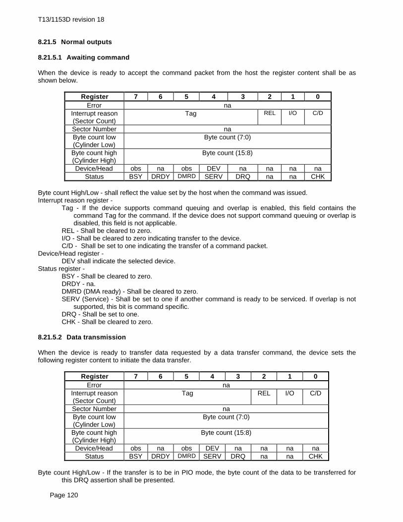
T13/1153D revision 18
Page 120
8.21.5 Normal outputs
8.21.5.1 Awaiting command
When the device is ready to accept the command packet from the host the register content shall be asshown below.
Register 7 6 5 4 3 2 1 0Error na
Interrupt reason(Sector Count)
Tag REL I/O C/D
Sector Number naByte count low(Cylinder Low)
Byte count (7:0)
Byte count high(Cylinder High)
Byte count (15:8)
Device/Head obs na obs DEV na na na naStatus BSY DRDY DMRD SERV DRQ na na CHK
Byte count High/Low - shall reflect the value set by the host when the command was issued.Interrupt reason register -
Tag - If the device supports command queuing and overlap is enabled, this field contains thecommand Tag for the command. If the device does not support command queuing or overlap isdisabled, this field is not applicable.
REL - Shall be cleared to zero.I/O - Shall be cleared to zero indicating transfer to the device.C/D - Shall be set to one indicating the transfer of a command packet.
Device/Head register -DEV shall indicate the selected device.
Status register -BSY - Shall be cleared to zero.DRDY - na.DMRD (DMA ready) - Shall be cleared to zero.SERV (Service) - Shall be set to one if another command is ready to be serviced. If overlap is not
supported, this bit is command specific.DRQ - Shall be set to one.CHK - Shall be cleared to zero.
8.21.5.2 Data transmission
When the device is ready to transfer data requested by a data transfer command, the device sets thefollowing register content to initiate the data transfer.
Register 7 6 5 4 3 2 1 0Error na
Interrupt reason(Sector Count)
Tag REL I/O C/D
Sector Number naByte count low(Cylinder Low)
Byte count (7:0)
Byte count high(Cylinder High)
Byte count (15:8)
Device/Head obs na obs DEV na na na naStatus BSY DRDY DMRD SERV DRQ na na CHK
Byte count High/Low - If the transfer is to be in PIO mode, the byte count of the data to be transferred forthis DRQ assertion shall be presented.

T13/1153D revision 18
Page 121
Valid byte count values are as follows:1) the byte count shall be less than or equal to the byte count limit value from the host;2) the byte count shall not be zero;3) the byte count shall be less than or equal to FFFEh;4) the byte count shall be even except for the last transfer of a command;5) if the byte count is odd, the last valid byte transferred is on DD[7:0] and the data on
DD[15:8] is a pad byte of undefined value;6) if the last transfer of a command has a pad byte, the byte count shall be odd.
Interrupt reason register -Tag - If the device supports command queuing and overlap is enabled, this field contains the
command Tag for the command. If the device does not support command queuing or overlap isdisabled, this field is not applicable.
REL - Shall be cleared to zero.I/O - Shall be cleared to zero if the transfer is to the device. Shall be set to one if the transfer is to
the host.C/D - Shall be cleared to zero indicating the transfer of data.
Device/Head register -DEV shall indicate the selected device.
Status register -BSY - Shall be cleared to zero.DRDY - na.DMRD (DMA ready) - Shall be set to one if the transfer is to be a DMA or Ultra DMA transfer and
the device supports overlap DMA.SERV (Service) - Shall be set to one if another command is ready to be serviced. If overlap is not
supported, this bit is command specific.DRQ - Shall be set to one.CHK - Shall be cleared to zero.
8.21.5.3 Bus release (overlap feature set only)
After receiving the command packet, the device sets BSY to one and clears DRQ to zero. If the commandpacket requires a data transfer, the OVL bit is set to one, and the device is not prepared to immediatelytransfer data, the device may perform a bus release by placing the following register content. If thecommand packet requires a data transfer, the OVL bit is set to one, and the Release interrupt is enabled,the device shall perform a bus release by setting the register content as follows.
Register 7 6 5 4 3 2 1 0Error na
Interrupt reason(Sector Count)
Tag REL I/O C/D
Sector Number naByte count low(Cylinder Low)
na
Byte count high(Cylinder High)
na
Device/Head obs na obs DEV na na na naStatus BSY DRDY DMRD SERV DRQ na na CHK
Byte count High/Low - na.Interrupt reason register -
Tag - If the device supports command queuing and overlap is enabled, this field contains thecommand Tag for the command. If the device does not support command queuing or overlap isdisabled, this field is not applicable.
REL - Shall be set to one.I/O - Shall be cleared to zero.C/D - Shall be cleared to zero.

T13/1153D revision 18
Page 122
Device/Head register -DEV shall indicate the selected device.
Status register -BSY - Shall be cleared to zero indicating bus release.DRDY - na.DMRD (DMA ready) - Shall be cleared to zero.SERV (Service) - Shall be set to one if another command is ready to be serviced. If overlap is not
supported, this bit is command specific.DRQ - Shall cleared to zero.CHK - Shall be cleared to zero.
8.21.5.4 Service request (overlap feature set only)
When the device is ready to transfer data or complete a command after the command has performed a busrelease, the device shall set the SERV bit and not change the state of any other register bit (see 6.6).
8.21.5.5 Successful command completion
When the device has command completion without error, the device sets the following register content.
Register 7 6 5 4 3 2 1 0Error na
Interrupt reason(Sector Count)
Tag REL I/O C/D
Sector Number naByte count low(Cylinder Low)
na
Byte count high(Cylinder High)
na
Device/Head obs na obs DEV na na na naStatus BSY DRDY DMRD SERV DRQ na na CHK
Byte count High/Low -na.Interrupt reason register -
Tag - If the device supports command queuing and overlap is enabled, this field contains thecommand Tag for the command. If the device does not support command queuing oroverlap is disabled, this field is not applicable.
REL - Shall be cleared to zero.I/O - Shall be set to one.C/D - Shall be set to one.
Device/Head register -DEV shall indicate the selected device.
Status register -BSY - Shall be cleared to zero indicating command completion.DRDY - Shall be set to one.DMRD (DMA ready) - na.SERV (Service) - Shall be set to one if another command is ready to be serviced. If overlap is not
supported, this bit is command specific.DRQ - Shall be cleared to zero.CHK - Shall be cleared to zero.
8.21.6 Error outputs
The device shall not terminate the PACKET command with an error before the last byte of the commandpacket has been written (see 9.11).

T13/1153D revision 18
Page 123
Register 7 6 5 4 3 2 1 0Error Sense key na ABRT EOM ILI
Interrupt reason(Sector Count)
Tag REL I/O C/D
Sector Number naCylinder Low naCylinder High naDevice/Head obs na obs DEV na na na na
Status BSY DRDY DF SERV DRQ na na CHK
Error register -Sense Key is a command packet set specific error indication.ABRT shall be set to one if the requested command has been command aborted because the
command code or a command parameter is invalid. ABRT may be set to one if the device isnot able to complete the action requested by the command.
EOM - the meaning of this bit is command set specific. See the appropriate command set standardfor its definition.
ILI - the meaning of this bit is command set specific. See the appropriate command set standard forits definition.
Interrupt reason register -Tag - If the device supports command queuing and overlap is enabled, this field contains the
command Tag for the command. If the device does not support command queuing oroverlap is disabled, this field is not applicable.
REL - Shall be cleared to zero.I/O - Shall be set to one.C/D - Shall be set to one.
Device/Head register -DEV shall indicate the selected device.
Status register -BSY shall be cleared to zero indicating command completion.DRDY shall be set to one.SERV (Service) - Shall be set to one if another command is ready to be serviced. If overlap is not
supported, this bit is command specific.DF (Device Fault) shall be set to one if a device fault has occurred.DRQ shall be cleared to zero.CHK shall be set to one if an Error register sense key or code bit is set.
8.21.7 Prerequisites
This command shall be accepted regardless of the state of DRDY.
8.21.8 Description
The PACKET command is used to transfer a device command via a command packet. If the native form ofthe encapsulated command is shorter than the packet size reported in bits 1 and 0 of word 0 of theIDENTIFY PACKET DEVICE response, the encapsulated command shall begin at byte 0 of the packet.Packet bytes beyond the end of the encapsulated command are reserved.
If the device supports overlap, the OVL bit is set to one in the Features register and the Release interrupthas been disabled via the SET FEATURES command, the device may or may not perform a bus release. Ifthe device is ready for the data transfer, it may begin the transfer immediately as described in the non-overlapped protocol (see 9.11). If the data is not ready, the device may perform a bus release and completethe transfer after the execution of a SERVICE command.

T13/1153D revision 18
Page 124
8.22 READ BUFFER
8.22.1 Command code
E4h
8.22.2 Feature set
General feature set− Optional for devices not implementing the PACKET Command feature set.− Use prohibited for devices implementing the PACKET Command feature set.
8.22.3 Protocol
PIO data in (see 9.7).
8.22.4 Inputs
Register 7 6 5 4 3 2 1 0Features na
Sector Count naSector Number naCylinder Low naCylinder High naDevice/Head obs na obs DEV na na na naCommand E4h
Device/Head register -DEV shall indicate the selected device.
8.22.5 Normal outputs
Register 7 6 5 4 3 2 1 0Error na
Sector Count naSector Number naCylinder Low naCylinder High naDevice/Head obs na obs DEV na na na na
Status BSY DRDY DF na DRQ na na ERR
Device/Head register -DEV shall indicate the selected device.
Status register -BSY shall be cleared to zero indicating command completion.DRDY shall be set to one.DF (Device Fault) shall be cleared to zero.DRQ shall be cleared to zero.ERR shall be cleared to zero.
8.22.6 Error outputs
The device shall return command aborted if the command is not supported.

T13/1153D revision 18
Page 125
Register 7 6 5 4 3 2 1 0Error na na na na na ABRT na na
Sector Count naSector Number naCylinder Low naCylinder High naDevice/Head obs na obs DEV na na na na
Status BSY DRDY DF na DRQ na na ERR
Error register -ABRT shall be set to one if this command is not supported. ABRT may be set to one if the device is not able to complete the action requested by the command.
Device/Head register -DEV shall indicate the selected device.
Status register -BSY shall be cleared to zero indicating command completion.DRDY shall be set to one.DF (Device Fault) shall be set to one if a device fault has occurred.DRQ shall be cleared to zero.ERR shall be set to one if an Error register bit is set to one.
8.22.7 Prerequisites
DRDY set equal to one. A WRITE BUFFER command shall immediately proceed a READ BUFFERcommand.
8.22.8 Description
The READ BUFFER command enables the host to read the current contents of the device’s sector buffer.
The READ BUFFER and WRITE BUFFER commands shall be synchronized such that sequential WRITEBUFFER and READ BUFFER commands access the same 512 bytes within the buffer.

T13/1153D revision 18
Page 126
8.23 READ DMA
8.23.1 Command code
C8h or C9h
NOTE − The host should not use the C9h value.
8.23.2 Feature set
General feature set− Mandatory for devices not implementing the PACKET Command feature set.− Use prohibited for devices implementing the PACKET Command feature set.
8.23.3 Protocol
DMA (see 9.10).
8.23.4 Inputs
Register 7 6 5 4 3 2 1 0Features na
Sector Count Sector countSector Number Sector number or LBACylinder Low Cylinder low or LBACylinder High Cylinder high or LBADevice/Head obs LBA obs DEV Head number or LBA
Command C8h or C9h
Sector Count -number of sectors to be transferred. A value of 00h indicates that 256 sectors are to be transferred.
Sector Number -starting sector number or LBA address bits (7:0).
Cylinder Low -starting cylinder number bits (7:0) or LBA address bits (15:8).
Cylinder High -starting cylinder number bits (15:8) or LBA address bits (23:16).
Device/Head -bit 6 set to one if LBA address, cleared to zero if CHS address.DEV shall indicate the selected device.bits (3:0) starting head number or LBA address bits (27:24).
8.23.5 Normal outputs
Register 7 6 5 4 3 2 1 0Error na
Sector Count naSector Number naCylinder Low naCylinder High naDevice/Head obs na obs DEV na na na na
Status BSY DRDY DF na DRQ na na ERR

T13/1153D revision 18
Page 127
Device/Head register -DEV shall indicate the selected device.
Status register -BSY shall be cleared to zero indicating command completion.DRDY shall be set to one.DF (Device Fault) shall be cleared to zero.DRQ shall be cleared to zero.ERR shall be cleared to zero.
8.23.6 Error outputs
An unrecoverable error encountered during the execution of this command results in the termination of thecommand. The Command Block registers contain the address of the sector where the first unrecoverableerror occurred. The amount of data transferred is indeterminate.
Register 7 6 5 4 3 2 1 0Error ICRC UNC MC IDNF MCR ABRT NM obs
Sector Count naSector Number Sector number or LBACylinder Low Cylinder low or LBACylinder High Cylinder high or LBADevice/Head obs na obs DEV Head number or LBA
Status BSY DRDY DF na DRQ na na ERR
Error register -ICRC shall be set to one if an interface CRC error has occurred during an Ultra DMA data transfer.
The content of this bit is not applicable for Multiword DMA transfers.UNC shall be set to one if data is uncorrectableMC shall be set to one if the media in a removable media device changed since the issuance of the
last command. The device shall clear its internal media change detected state.IDNF shall be set to one if a user-accessible address could not be found and after an unsuccessful
INITIALIZE DEVICE PARAMETERS command until a valid CHS translation is established(see 8.16.8). IDNF shall be set to one if an address outside of the range of user-accessibleaddresses is requested if command aborted is not returned.
MCR shall be set to one if a media change request has been detected by a removable mediadevice. This bit is only cleared by a GET MEDIA STATUS or a media access command.
ABRT shall be set to one if this command is not supported or if an error, including an ICRC error,has occurred during an Ultra DMA data transfer. ABRT may be set to one if the device isnot able to complete the action requested by the command. ABRT shall be set to one if anaddress outside of the range of user-accessible addresses is requested if IDNF is not set toone.
NM shall be set to one if no media is present in a removable media device.Sector Number, Cylinder Low, Cylinder High, Device/Head -
shall be written with the address of first unrecoverable error.Device/Head register -
DEV shall indicate the selected device.Status register -
BSY shall be cleared to zero indicating command completion.DRDY shall be set to one.DF (Device Fault) shall be set to one if a device fault has occurred.DRQ shall be cleared to zero.ERR shall be set to one if an Error register bit is set to one.
8.23.7 Prerequisites
DRDY set equal to one. The host shall initialize the DMA channel.

T13/1153D revision 18
Page 128
8.23.8 Description
The READ DMA command allows the host to read data using the DMA data transfer protocol.
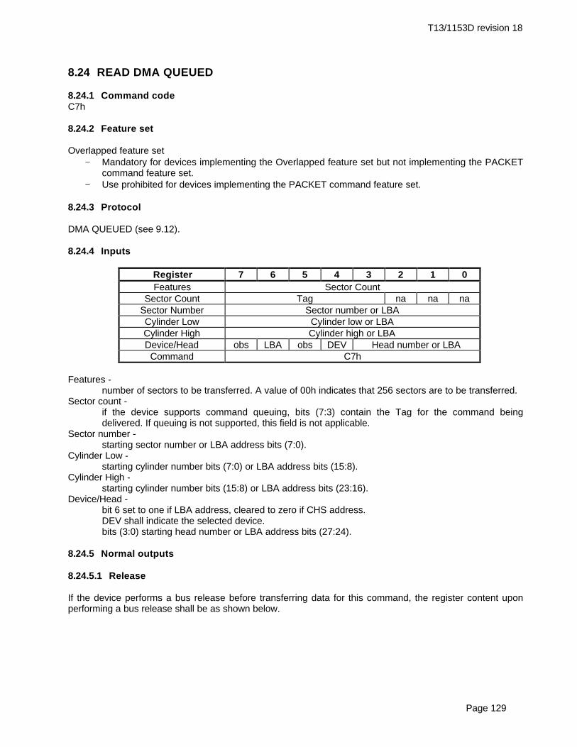
T13/1153D revision 18
Page 129
8.24 READ DMA QUEUED
8.24.1 Command codeC7h
8.24.2 Feature set
Overlapped feature set− Mandatory for devices implementing the Overlapped feature set but not implementing the PACKET
command feature set.− Use prohibited for devices implementing the PACKET command feature set.
8.24.3 Protocol
DMA QUEUED (see 9.12).
8.24.4 Inputs
Register 7 6 5 4 3 2 1 0Features Sector Count
Sector Count Tag na na naSector Number Sector number or LBACylinder Low Cylinder low or LBACylinder High Cylinder high or LBADevice/Head obs LBA obs DEV Head number or LBA
Command C7h
Features -number of sectors to be transferred. A value of 00h indicates that 256 sectors are to be transferred.
Sector count -if the device supports command queuing, bits (7:3) contain the Tag for the command beingdelivered. If queuing is not supported, this field is not applicable.
Sector number -starting sector number or LBA address bits (7:0).
Cylinder Low -starting cylinder number bits (7:0) or LBA address bits (15:8).
Cylinder High -starting cylinder number bits (15:8) or LBA address bits (23:16).
Device/Head -bit 6 set to one if LBA address, cleared to zero if CHS address.DEV shall indicate the selected device.bits (3:0) starting head number or LBA address bits (27:24).
8.24.5 Normal outputs
8.24.5.1 Release
If the device performs a bus release before transferring data for this command, the register content uponperforming a bus release shall be as shown below.

T13/1153D revision 18
Page 130
Register 7 6 5 4 3 2 1 0Error na
Sector Count Tag REL I/O C/DSector Number naCylinder Low naCylinder High naDevice/Head obs na obs DEV na
Status BSY DRDY DF SERV DRQ na na ERR
Sector Count register -Tag - If the device supports command queuing, this field shall contain the Tag of the command
being bus released. If the device does not support command queuing, this field shall bezeros.
REL bit shall be set to one indicating that the device has bus released an overlap command.I/O shall be zero.C/D shall be zero.
Device/Head register -DEV shall indicate the selected device.
Status register -BSY shall be cleared to zero indicating bus release.DRDY shall be set to one.SERV (Service) shall be cleared to zero when no other queued command is ready for service. It
shall be set to one when another queued command is ready for service. It shall be set toone when the device has prepared this command for service.
DF (Device Fault) shall be cleared to zeroDRQ bit shall be cleared to zero.ERR bit shall be cleared to zero.
8.24.5.2 Command completion
When the transfer of all requested data has occurred without error, the register content shall be as shownbelow.
Register 7 6 5 4 3 2 1 0Error 00h
Sector Count Tag REL I/O C/DSector Number naCylinder Low naCylinder High naDevice/Head obs na obs DEV na
Status BSY DRDY DF SERV DRQ na na ERR
Sector Count register -Tag - If the device supports command queuing, this field shall contain the Tag of the completed
command. If the device does not support command queuing, this field shall be zeros.REL shall be cleared to zero.I/O shall be set to one.C/D shall be set to one.
Device/Head register -DEV shall indicate the selected device.
Status register -BSY shall be cleared to zero indicating command completion.DRDY shall be set to one.SERV (Service) shall be cleared to zero when no other queued command is ready for service. It
shall be set to one when another queued command is ready for service.DF (Device Fault) shall be cleared to zero.

T13/1153D revision 18
Page 131
DRQ bit shall be cleared to zero.ERR bit shall be cleared to zero.
8.24.6 Error outputsThe Sector Count register contains the Tag for this command if the device supports command queuing. Thedevice shall return command aborted if the command is not supported or if the device has not hadoverlapped interrupt enabled. The device shall return command aborted if the device supports commandqueuing and the Tag is invalid. An unrecoverable error encountered during the execution of this commandresults in the termination of the command and the Command Block registers contain the sector where thefirst unrecoverable error occurred. If a queue existed, the unrecoverable error shall cause the queue toabort.
Register 7 6 5 4 3 2 1 0Error ICRC UNC MC IDNF MCR ABRT NM obs
Sector Count Tag REL I/O C/DSector Number Sector number or LBACylinder Low Cylinder low or LBACylinder High Cylinder high or LBADevice/Head obs na obs D Head number or LBA
Status BSY DRDY DF SERV DRQ na na ERR
Error register -ICRC shall be set to one if an interface CRC error has occurred during an Ultra DMA data transfer.
The content of this bit is not applicable for Multiword DMA transfers.UNC shall be set to one if data is uncorrectable.MC shall be set to one if the media in a removable media device changed since the issuance of the
last command. The device shall clear its internal media change detected state.IDNF shall be set to one if a user-accessible address could not be found and after an unsuccessful
INITIALIZE DEVICE PARAMETERS command until a valid CHS translation is established(see 8.16.8). IDNF shall be set to one if an address outside of the range of user-accessibleaddresses is requested if ABRT is not set to one.
MCR shall be set to one if a media change request has been detected by a removable mediadevice. This bit is only cleared by a GET MEDIA STATUS or a media access command.
ABRT shall be set to one if this command is not supported or if an error, including an ICRC error,has occurred during an Ultra DMA data transfer. ABRT may be set to one if the device isnot able to complete the action requested by the command. ABRT shall be set to one if anaddress outside of the range of user-accessible addresses is requested if IDNF is not set toone.
NM shall be set to one if no media is present in a removable media device.Sector Count register -
Tag - If the device supports command queuing, this field shall contain the Tag of the completedcommand. If the device does not support command queuing, this field shall be zeros.
REL shall be cleared to zero.I/O shall be set to one.Bit 0 - C/D shall be set to one.
Sector Number, Cylinder Low, Cylinder High, Device/Head -shall be written with the address of first unrecoverable error.DEV shall indicate the selected device.
Status register -BSY shall be cleared to zero indicating command completion.DRDY shall be set to one.DF (Device Fault) shall be set to one if a device fault has occurred.SERV (Service) shall be cleared to zero when no other queued command is ready for service. It
shall be set to one when another queued command is ready for service.DRQ shall be cleared to zero.ERR shall be set to one if an Error register bit is set to one.

T13/1153D revision 18
Page 132
8.24.7 PrerequisitesDRDY set to one. The host shall initialize the DMA channel.
8.24.8 DescriptionThis command executes in a similar manner to a READ DMA command. The device may perform a busrelease or it may execute the data transfer without performing a bus release if the data is ready to transfer.

T13/1153D revision 18
Page 133
8.25 READ MULTIPLE
8.25.1 Command code
C4h
8.25.2 Feature set
General feature set− Mandatory for devices not implementing the PACKET Command feature set.− Use prohibited for devices implementing the PACKET Command feature set.
8.25.3 Protocol
PIO data in (see 9.7).
8.25.4 Inputs
Register 7 6 5 4 3 2 1 0Features na
Sector Count Sector countSector Number Sector number or LBACylinder Low Cylinder low or LBACylinder High Cylinder high or LBADevice/Head obs LBA obs DEV Head number or LBACommand C4h
Sector Count -number of sectors to be transferred. A value of 00h indicates that 256 sectors are to be transferred.
Sector Number -starting sector number or LBA address bits (7:0).
Cylinder Low -starting cylinder number bits (7:0) or LBA address bits (15:8).
Cylinder High -starting cylinder number bits (15:8) or LBA address bits (23:16).
Device/Head -bit 6 set to one if LBA address, cleared to zero if CHS address.DEV shall indicate the selected device.bits (3:0) starting head number or LBA address bits (27:24).
8.25.5 Normal outputs
Register 7 6 5 4 3 2 1 0Error na
Sector Count naSector Number naCylinder Low naCylinder High naDevice/Head obs na obs DEV na na na na
Status BSY DRDY DF na DRQ na na ERR
Device/Head register -DEV shall indicate the selected device.
Status register -BSY shall be cleared to zero indicating command completion.

T13/1153D revision 18
Page 134
DRDY shall be set to one.DF (Device Fault) shall be cleared to zero.DRQ shall be cleared to zero.ERR shall be cleared to zero.
8.25.6 Error outputs
An unrecoverable error encountered during the execution of this command results in the termination of thecommand. The Command Block registers contain the address of the sector where the first unrecoverableerror occurred. The amount of data transferred is indeterminate.
Register 7 6 5 4 3 2 1 0Error na UNC MC IDNF MCR ABRT NM obs
Sector Count naSector Number Sector number or LBACylinder Low Cylinder low or LBACylinder High Cylinder high or LBADevice/Head obs na obs DEV Head number or LBA
Status BSY DRDY DF na DRQ na na ERR
Error register -UNC shall be set to one if data is uncorrectable.MC shall be set to one if the media in a removable media device changed since the issuance of the
last command. The device shall clear its internal media change detected state.IDNF shall be set to one if a user-accessible address could not be found and after an unsuccessful
INITIALIZE DEVICE PARAMETERS command until a valid CHS translation is established(see 8.16.8). IDNF shall be set to one if an address outside of the range of user-accessibleaddresses is requested if command aborted is not returned.
MCR shall be set to one if a media change request has been detected by a removable mediadevice. This bit is only cleared by a GET MEDIA STATUS or a media access command.
ABRT shall be set to one if this command is not supported or if an error, including an ICRC error,has occurred during an Ultra DMA data transfer. ABRT may be set to one if the device isnot able to complete the action requested by the command. ABRT shall be set to one if anaddress outside of the range of user-accessible addresses is requested if IDNF is not set toone.
NM shall be set to one if no media is present in a removable media device.Sector Number, Cylinder Low, Cylinder High, Device/Head -
shall be written with the address of first unrecoverable error.DEV shall indicate the selected device.
Status register -BSY shall be cleared to zero indicating command completion.DRDY shall be set to one.DF (Device Fault) shall be set to one if a device fault has occurred.DRQ shall be cleared to zero.ERR shall be set to one if an Error register bit is set to one.
8.25.7 Prerequisites
DRDY set equal to one. If bit 8 of IDENTIFY DEVICE word 59 is cleared to zero, a successful SETMULTIPLE MODE command shall precede a READ MULTIPLE command.
8.25.8 Description
The READ MULTIPLE command performs similarly to the READ SECTOR(S) command. Interrupts are notgenerated on every sector, but on the transfer of a block that contains the number of sectors defined by aSET MULTIPLE MODE command or the default if no intervening SET MULTIPLE command has beenissued. Command execution is identical to the READ SECTOR(S) operation except that the number of
T13/1153D revision 18
Page 135
sectors defined by a SET MULTIPLE MODE command are transferred without intervening interrupts. TheDRQ bit qualification of the transfer is required only at the start of the data block, not on each sector.
The block count of sectors to be transferred without intervening interrupts is programmed by the SETMULTIPLE MODE command, that shall be executed prior to the READ MULTIPLE command. When theREAD MULTIPLE command is issued, the Sector Count register contains the number of sectors (not thenumber of blocks or the block count) requested.
If the number of requested sectors is not evenly divisible by the block count, as many full blocks as possibleare transferred, followed by a final, partial block transfer. The partial block transfer shall be for n sectors,where n = remainder (sector count/ block count).
If the READ MULTIPLE command is received when READ MULTIPLE commands are disabled, the READMULTIPLE operation shall be rejected with command aborted.
Device errors encountered during READ MULTIPLE commands are posted at the beginning of the block orpartial block transfer, but the DRQ bit is still set to one and the data transfer shall take place, includingtransfer of corrupted data, if any. The contents of the Command Block Registers following the transfer of adata block that had a sector in error are undefined. The host should retry the transfer as individual requeststo obtain valid error information.
Subsequent blocks or partial blocks are transferred only if the error was a correctable data error. All othererrors cause the command to stop after transfer of the block that contained the error.
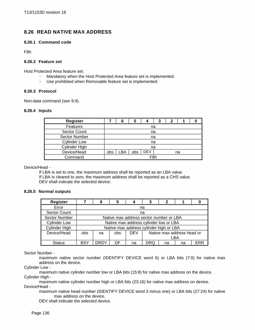
T13/1153D revision 18
Page 136
8.26 READ NATIVE MAX ADDRESS
8.26.1 Command code
F8h
8.26.2 Feature set
Host Protected Area feature set.− Mandatory when the Host Protected Area feature set is implemented.− Use prohibited when Removable feature set is implemented.
8.26.3 Protocol
Non-data command (see 9.9).
8.26.4 Inputs
Register 7 6 5 4 3 2 1 0Features na
Sector Count naSector Number naCylinder Low naCylinder High naDevice/Head obs LBA obs DEV naCommand F8h
Device/Head -If LBA is set to one, the maximum address shall be reported as an LBA value.If LBA is cleared to zero, the maximum address shall be reported as a CHS value.DEV shall indicate the selected device.
8.26.5 Normal outputs
Register 7 6 5 4 3 2 1 0Error na
Sector Count naSector Number Native max address sector number or LBACylinder Low Native max address cylinder low or LBACylinder High Native max address cylinder high or LBADevice/Head obs na obs DEV Native max address head or
LBAStatus BSY DRDY DF na DRQ na na ERR
Sector Number -maximum native sector number (IDENTIFY DEVICE word 6) or LBA bits (7:0) for native maxaddress on the device.
Cylinder Low -maximum native cylinder number low or LBA bits (15:8) for native max address on the device.
Cylinder High -maximum native cylinder number high or LBA bits (23:16) for native max address on device.
Device/Head -maximum native head number (IDENTIFY DEVICE word 3 minus one) or LBA bits (27:24) for native
max address on the device.DEV shall indicate the selected device.

T13/1153D revision 18
Page 137
Status register -BSY shall be cleared to zero indicating command completion.DRDY shall be set to one.DF (Device Fault) shall be cleared to zero.DRQ shall be cleared to zero.ERR shall be cleared to zero.
8.26.6 Error outputs
If this command is not supported the device shall return command aborted. The device shall returncommand aborted if a CHS address is requested and the device does not support a CHS translation.
Register 7 6 5 4 3 2 1 0Error na na na na na ABRT na na
Sector Count naSector Number naCylinder Low naCylinder High naDevice/Head obs na obs DEV na
Status BSY DRDY na na na na na ERR
Error register -ABRT shall be set to one if this command is not supported. ABRT may be set to one if the device is not able to complete the action requested by the command.
Device/Head register -DEV shall indicate the selected device.
Status register -BSY shall be cleared to zero indicating command completion.DRDY shall be set to one.ERR shall be set to one if an Error register bit is set to one.
8.26.7 Prerequisites
DRDY set equal to one.
8.26.8 Description
This command returns the native maximum address. The native maximum address is the highest addressaccepted by the device in the factory default condition. The native maximum address is the maximumaddress that is valid when using the SET MAX ADDRESS command.
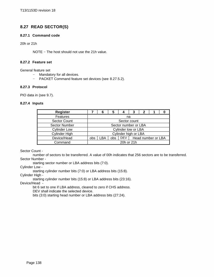
T13/1153D revision 18
Page 138
8.27 READ SECTOR(S)
8.27.1 Command code
20h or 21h
NOTE − The host should not use the 21h value.
8.27.2 Feature set
General feature set− Mandatory for all devices.− PACKET Command feature set devices (see 8.27.5.2).
8.27.3 Protocol
PIO data in (see 9.7).
8.27.4 Inputs
Register 7 6 5 4 3 2 1 0Features na
Sector Count Sector countSector Number Sector number or LBACylinder Low Cylinder low or LBACylinder High Cylinder high or LBADevice/Head obs LBA obs DEV Head number or LBACommand 20h or 21h
Sector Count -number of sectors to be transferred. A value of 00h indicates that 256 sectors are to be transferred.
Sector Number -starting sector number or LBA address bits (7:0).
Cylinder Low -starting cylinder number bits (7:0) or LBA address bits (15:8).
Cylinder High -starting cylinder number bits (15:8) or LBA address bits (23:16).
Device/Head -bit 6 set to one if LBA address, cleared to zero if CHS address.DEV shall indicate the selected device.bits (3:0) starting head number or LBA address bits (27:24).

T13/1153D revision 18
Page 139
8.27.5 Outputs
8.27.5.1 Normal outputs
Register 7 6 5 4 3 2 1 0Error na
Sector Count naSector Number naCylinder Low naCylinder High naDevice/Head obs na obs DEV na na na na
Status BSY DRDY DF na DRQ na na ERR
Device/Head register -DEV shall indicate the selected device.
Status register -BSY shall be cleared to zero indicating command completion.DRDY shall be set to one.DF (Device Fault) shall be cleared to zero.DRQ shall be cleared to zero.ERR shall be cleared to zero.
8.27.5.2 Outputs for PACKET Command feature set devices
In response to this command, devices that implement the PACKET Command feature set shall postcommand aborted and place the PACKET Command feature set signature in the Cylinder High and theCylinder Low register (see 9.1).
8.27.6 Error outputs
An unrecoverable error encountered during the execution of this command results in the termination of thecommand. The Command Block registers contain the address of the sector where the first unrecoverableerror occurred. The amount of data transferred is indeterminate.
Register 7 6 5 4 3 2 1 0Error na UNC MC IDNF MCR ABRT NM obs
Sector Count naSector Number Sector number or LBACylinder Low Cylinder low or LBACylinder High Cylinder high or LBADevice/Head obs na obs DEV Head number or LBA
Status BSY DRDY DF na DRQ na na ERR
Error register -UNC shall be set to one if data is uncorrectable.MC shall be set to one if the media in a removable media device changed since the issuance of the
last command. The device shall clear its internal media change detected state.IDNF shall be set to one if a user-accessible address could not be found and after an unsuccessful
INITIALIZE DEVICE PARAMETERS command until a valid CHS translation is established(see 8.16.8). IDNF shall be set to one if an address outside of the range of user-accessibleaddresses is requested if command aborted is not returned.
MCR shall be set to one if a media change request has been detected by a removable mediadevice. This bit is only cleared by a GET MEDIA STATUS or a media access command.
ABRT shall be set to one if this command is not supported or if an error, including an ICRC error,has occurred during an Ultra DMA data transfer. ABRT may be set to one if the device isnot able to complete the action requested by the command. ABRT shall be set to one if an

T13/1153D revision 18
Page 140
address outside of the range of user-accessible addresses is requested if IDNF is not set toone.
NM shall be set to one if no media is present in a removable media device.Sector Number, Cylinder Low, Cylinder High, Device/Head -
shall be written with the address of first unrecoverable error.DEV shall indicate the selected device.
Status register -BSY shall be cleared to zero indicating command completion.DRDY shall be set to one.DF (Device Fault) shall be set to one if a device fault has occurred.DRQ shall be cleared to zero.ERR shall be set to one if an Error register bit is set to one.
8.27.7 Prerequisites
DRDY set equal to one.
8.27.8 Description
This command reads from 1 to 256 sectors as specified in the Sector Count register. A sector count of 0requests 256 sectors. The transfer shall begin at the sector specified in the Sector Number register.
The DRQ bit is always set to one prior to data transfer regardless of the presence or absence of an errorcondition.
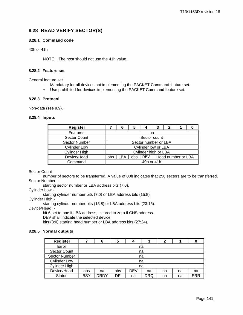
T13/1153D revision 18
Page 141
8.28 READ VERIFY SECTOR(S)
8.28.1 Command code
40h or 41h
NOTE − The host should not use the 41h value.
8.28.2 Feature set
General feature set− Mandatory for all devices not implementing the PACKET Command feature set.− Use prohibited for devices implementing the PACKET Command feature set.
8.28.3 Protocol
Non-data (see 9.9).
8.28.4 Inputs
Register 7 6 5 4 3 2 1 0Features na
Sector Count Sector countSector Number Sector number or LBACylinder Low Cylinder low or LBACylinder High Cylinder high or LBADevice/Head obs LBA obs DEV Head number or LBACommand 40h or 41h
Sector Count -number of sectors to be transferred. A value of 00h indicates that 256 sectors are to be transferred.
Sector Number -starting sector number or LBA address bits (7:0).
Cylinder Low -starting cylinder number bits (7:0) or LBA address bits (15:8).
Cylinder High -starting cylinder number bits (15:8) or LBA address bits (23:16).
Device/Head -bit 6 set to one if LBA address, cleared to zero if CHS address.DEV shall indicate the selected device.bits (3:0) starting head number or LBA address bits (27:24).
8.28.5 Normal outputs
Register 7 6 5 4 3 2 1 0Error na
Sector Count naSector Number naCylinder Low naCylinder High naDevice/Head obs na obs DEV na na na na
Status BSY DRDY DF na DRQ na na ERR

T13/1153D revision 18
Page 142
Device/Head register -DEV shall indicate the selected device.
Status register -BSY shall be cleared to zero indicating command completion.DRDY shall be set to one.DF (Device Fault) shall be cleared to zero.DRQ shall be cleared to zero.ERR shall be cleared to zero.
8.28.6 Error outputs
An unrecoverable error encountered during the execution of this command results in the termination of thecommand. The Command Block registers contain the address of the sector where the first unrecoverableerror occurred.
Register 7 6 5 4 3 2 1 0Error na UNC MC IDNF MCR ABRT NM obs
Sector Count naSector Number Sector number or LBACylinder Low Cylinder low or LBACylinder High Cylinder high or LBADevice/Head obs na obs DEV Head number or LBA
Status BSY DRDY DF na DRQ na na ERR
Error register -UNC shall be set to one if data is uncorrectable.MC shall be set to one if the media in a removable media device changed since the issuance of the
last command. The device shall clear its internal media change detected state.IDNF shall be set to one if a user-accessible address could not be found and after an unsuccessful
INITIALIZE DEVICE PARAMETERS command until a valid CHS translation is established(see 8.16.8). IDNF shall be set to one if an address outside of the range of user-accessibleaddresses is requested if command aborted is not returned.
MCR shall be set to one if a media change request has been detected by a removable mediadevice. This bit is only cleared by a GET MEDIA STATUS or a media access command.
ABRT shall be set to one if this command is not supported or if an error, including an ICRC error,has occurred during an Ultra DMA data transfer. ABRT may be set to one if the device isnot able to complete the action requested by the command. ABRT shall be set to one if anaddress outside of the range of user-accessible addresses is requested if IDNF is not set toone.
NM shall be set to one if no media is present in a removable media device.Sector Number, Cylinder Low, Cylinder High, Device/Head -
shall be written with the address of first unrecoverable error.DEV shall indicate the selected device.
Status register -BSY shall be cleared to zero indicating command completion.DRDY shall be set to one.DF (Device Fault) shall be set to one if a device fault has occurred.DRQ shall be cleared to zero.ERR shall be set to one if an Error register bit is set to one.
8.28.7 Prerequisites
DRDY set equal to one.
8.28.8 Description

T13/1153D revision 18
Page 143
This command is identical to the READ SECTOR(S) command, except that the DRQ bit is never set to one,and no data is transferred to the host.

T13/1153D revision 18
Page 144
8.29 SECURITY DISABLE PASSWORD
8.29.1 Command code
F6h
8.29.2 Feature set
Security Mode feature set.− Mandatory when the Security Mode feature set is implemented.
8.29.3 Protocol
PIO data out (see 9.8).
8.29.4 Inputs
Register 7 6 5 4 3 2 1 0Features na
Sector Count naSector Number naCylinder Low naCylinder High naDevice/Head obs na obs DEV na na na naCommand F6h
Device/Head register -DEV shall indicate the selected device.
8.29.5 Normal outputs
Register 7 6 5 4 3 2 1 0Error na
Sector Count naSector Number naCylinder Low naCylinder High naDevice/Head obs na obs DEV na na na na
Status BSY DRDY DF na DRQ na na ERR
Device/Head register -DEV shall indicate the selected device.
Status register -BSY shall be cleared to zero indicating command completion.DRDY shall be set to one.DF (Device Fault) shall be cleared to zero.DRQ shall be cleared to zero.ERR shall be cleared to zero.
8.29.6 Error outputs
The device shall return command aborted if the command is not supported, the device is in Locked mode,or the device is in Frozen mode.

T13/1153D revision 18
Page 145
Register 7 6 5 4 3 2 1 0Error na na na na na ABRT na na
Sector Count naSector Number naCylinder Low naCylinder High naDevice/Head obs na obs DEV na
Status BSY DRDY DF na DRQ na na ERR
Error register -ABRT shall be set to one if this command is not supported. ABRT may be set to one if the device is not able to complete the action requested by the command.
Device/Head register -DEV shall indicate the selected device.
Status register -BSY shall be cleared to zero indicating command completion.DRDY shall be set to one.DF (Device Fault) shall be set to one if a device fault has occurred.DRQ shall be cleared to zero.ERR shall be set to one if an Error register bit is set to one.
8.29.7 Prerequisites
DRDY set equal to one. Device shall be in Unlocked mode.
8.29.8 Description
The SECURITY DISABLE PASSWORD command requests a transfer of a single sector of data from thehost. Table 15 defines the content of this sector of information. If the password selected by word 0 matchesthe password previously saved by the device, the device disables the Lock mode. This command does notchange the Master password that may be reactivated later by setting a User password (see 6.10).
Table 15 −− Security password contentWord Content
0 Control wordBit 0 Identifier 0=compare User password
1=compare Master passwordBit 1-15 Reserved
1-16 Password (32 bytes)17-255 Reserved
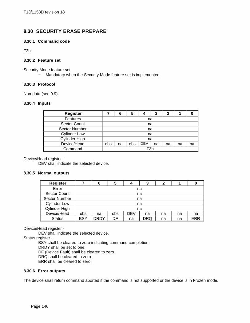
T13/1153D revision 18
Page 146
8.30 SECURITY ERASE PREPARE
8.30.1 Command code
F3h
8.30.2 Feature set
Security Mode feature set.− Mandatory when the Security Mode feature set is implemented.
8.30.3 Protocol
Non-data (see 9.9).
8.30.4 Inputs
Register 7 6 5 4 3 2 1 0Features na
Sector Count naSector Number naCylinder Low naCylinder High naDevice/Head obs na obs DEV na na na naCommand F3h
Device/Head register -DEV shall indicate the selected device.
8.30.5 Normal outputs
Register 7 6 5 4 3 2 1 0Error na
Sector Count naSector Number naCylinder Low naCylinder High naDevice/Head obs na obs DEV na na na na
Status BSY DRDY DF na DRQ na na ERR
Device/Head register -DEV shall indicate the selected device.
Status register -BSY shall be cleared to zero indicating command completion.DRDY shall be set to one.DF (Device Fault) shall be cleared to zero.DRQ shall be cleared to zero.ERR shall be cleared to zero.
8.30.6 Error outputs
The device shall return command aborted if the command is not supported or the device is in Frozen mode.

T13/1153D revision 18
Page 147
Register 7 6 5 4 3 2 1 0Error na na na na na ABRT na na
Sector Count naSector Number naCylinder Low naCylinder High naDevice/Head obs na obs DEV na
Status BSY DRDY DF na DRQ na na ERR
Error register -ABRT shall be set to one if this command is not supported or device is in Frozen mode. ABRT may be set to one if the device is not able to complete the action requested by the command.
Device/Head register -DEV shall indicate the selected device.
Status register -BSY shall be cleared to zero indicating command completion.DRDY shall be set to one.DF (Device Fault) shall be set to one if a device fault has occurred.DRQ shall be cleared to zero.ERR shall be set to one if an Error register bit is set to one.
8.30.7 Prerequisites
DRDY set equal to one.
8.30.8 Description
The SECURITY ERASE PREPARE command shall be issued immediately before the SECURITY ERASEUNIT command to enable device erasing and unlocking. This command prevents accidental erase of thedevice.

T13/1153D revision 18
Page 148
8.31 SECURITY ERASE UNIT
8.31.1 Command code
F4h
8.31.2 Feature set
Security Mode feature set.− Mandatory when the Security Mode feature set is implemented.
8.31.3 Protocol
PIO data out (see 9.8).
8.31.4 Inputs
Register 7 6 5 4 3 2 1 0Features na
Sector Count naSector Number naCylinder Low naCylinder High naDevice/Head obs na obs DEV na na na naCommand F4h
Device/Head register -DEV shall indicate the selected device.
8.31.5 Normal outputs
Register 7 6 5 4 3 2 1 0Error na
Sector Count naSector Number naCylinder Low naCylinder High naDevice/Head obs na obs DEV na na na na
Status BSY DRDY DF na DRQ na na ERR
Device/Head register -DEV shall indicate the selected device.
Status register -BSY shall be cleared to zero indicating command completion.DRDY shall be set to one.DF (Device Fault) shall be cleared to zero.DRQ shall be cleared to zero.ERR shall be cleared to zero.

T13/1153D revision 18
Page 149
8.31.6 Error outputs
The device shall return command aborted if the command is not supported, the device is in Frozen mode,not preceded by a SECURITY ERASE PREPARE command, or if the data area is not successfullyoverwritten.
Register 7 6 5 4 3 2 1 0Error na na na na na ABRT na na
Sector Count naSector Number naCylinder Low naCylinder High naDevice/Head obs na obs DEV na
Status BSY DRDY DF na DRQ na na ERR
Error register -ABRT shall be set to one if this command is not supported, device is in Frozen mode, not preceded
by a SECURITY ERASE PREPARE command, or if the data area is not successfullyoverwritten. ABRT may be set to one if the device is not able to complete the actionrequested by the command.
Device/Head register -DEV shall indicate the selected device.
Status register -BSY shall be cleared to zero indicating command completion.DRDY shall be set to one.DF (Device Fault) shall be set to one if a device fault has occurred.DRQ shall be cleared to zero.ERR shall be set to one if an Error register bit is set to one.
8.31.7 Prerequisites
DRDY set equal to one. This command shall be immediately preceded by a SECURITY ERASE PREPAREcommand.
8.31.8 Description
This command requests transfer of a single sector of data from the host. Table 16 defines the content of thissector of information. If the password does not match the password previously saved by the device, thedevice rejects the command with command aborted.
The SECURITY ERASE PREPARE command shall be completed immediately prior to the SECURITYERASE UNIT command. If the device receives a SECURITY ERASE UNIT command without animmediately prior SECURITY ERASE PREPARE command, the device command aborts the SECURITYERASE UNIT command.
When normal erase mode is selected, the SECURITY ERASE UNIT command writes binary zeroes to alluser data areas. The enhanced erase mode is optional. When enhanced erase mode is selected, the devicewrites predetermined data patterns to all user data areas. In enhanced mode, all previously written user datais overwritten, including sectors that are no longer in use due to reallocation.
This command disables the device Lock mode, however, the Master password is still stored internally withinthe device and may be reactivated later when a new User password is set.

T13/1153D revision 18
Page 150
Table 16 −− SECURITY ERASE UNIT passwordWord Content
0 Control wordBit 0 Identifier 0=compare User password
1=compare Master passwordBit 1 Erase mode 0=Normal erase
1=Enhanced eraseBit 2-15 Reserved
1-16 Password (32 bytes)17-255 Reserved

T13/1153D revision 18
Page 151
8.32 SECURITY FREEZE LOCK
8.32.1 Command code
F5h
8.32.2 Feature set
Security Mode feature set.− Mandatory when the Security Mode feature set is implemented.
8.32.3 Protocol
Non-data (see 9.9).
8.32.4 Inputs
Register 7 6 5 4 3 2 1 0Features na
Sector Count naSector Number naCylinder Low naCylinder High naDevice/Head obs na obs DEV na na na naCommand F5h
Device/Head register -DEV shall indicate the selected device.
8.32.5 Normal outputs
Register 7 6 5 4 3 2 1 0Error na
Sector Count naSector Number naCylinder Low naCylinder High naDevice/Head obs na obs DEV na na na na
Status BSY DRDY DF na DRQ na na ERR
Device/Head register -DEV shall indicate the selected device.
Status register -BSY shall be cleared to zero indicating command completion.DRDY shall be set to one.DF (Device Fault) shall be cleared to zero.DRQ shall be cleared to zero.ERR shall be cleared to zero.
8.32.6 Error outputs
The device shall return command aborted if the command is not supported, or the device is in Lockedmode.

T13/1153D revision 18
Page 152
Register 7 6 5 4 3 2 1 0Error na na na na na ABRT na na
Sector Count naSector Number naCylinder Low naCylinder High naDevice/Head obs na obs DEV na
Status BSY DRDY DF na DRQ na na ERR
Error register -ABRT shall be set to one if this command is not supported or device is in locked mode. ABRT may be set to one if the device is not able to complete the action requested by the command.
Device/Head register -DEV shall indicate the selected device.
Status register -BSY shall be cleared to zero indicating command completion.DRDY shall be set to one.DF (Device Fault) shall be set to one if a device fault has occurred.DRQ shall be cleared to zero.ERR shall be set to one if an Error register bit is set to one.
8.32.7 Prerequisites
DRDY set equal to one.
8.32.8 Description
The SECURITY FREEZE LOCK command sets the device to Frozen mode. After command completion anyother commands that update the device Lock mode are rejected. Frozen mode is disabled by power off orhardware reset. If SECURITY FREEZE LOCK is issued when the device is in Frozen mode, the commandexecutes and the device remains in Frozen mode.
Commands disabled by SECURITY FREEZE LOCK are:− SECURITY SET PASSWORD− SECURITY UNLOCK− SECURITY DISABLE PASSWORD− SECURITY ERASE UNIT

T13/1153D revision 18
Page 153
8.33 SECURITY SET PASSWORD
8.33.1 Command code
F1h
8.33.2 Feature set
Security Mode feature set.− Mandatory when the Security Mode feature set is implemented.
8.33.3 Protocol
PIO data out (see 9.8).
8.33.4 Inputs
Register 7 6 5 4 3 2 1 0Features na
Sector Count naSector Number naCylinder Low naCylinder High naDevice/Head obs na obs DEV na na na naCommand F1h
Device/Head register -DEV shall indicate the selected device.
8.33.5 Normal outputs
Register 7 6 5 4 3 2 1 0Error na
Sector Count naSector Number naCylinder Low naCylinder High naDevice/Head obs na obs DEV na na na na
Status BSY DRDY DF na DRQ na na ERR
Device/Head register -DEV shall indicate the selected device.
Status register -BSY shall be cleared to zero indicating command completion.DRDY shall be set to one.DF (Device Fault) shall be cleared to zero.DRQ shall be cleared to zero.ERR shall be cleared to zero.
8.33.6 Error outputs
The device shall return command aborted if the command is not supported, the device is in Locked mode,or the device is in Frozen mode.

T13/1153D revision 18
Page 154
Register 7 6 5 4 3 2 1 0Error na na na na na ABRT na na
Sector Count naSector Number naCylinder Low naCylinder High naDevice/Head obs na obs DEV na
Status BSY DRDY DF na DRQ na na ERR
Error register -ABRT shall be set to one if this command is not supported, if device is in Frozen mode, or if device
is in locked mode. ABRT may be set to one if the device is not able to complete the actionrequested by the command.
Device/Head register -DEV shall indicate the selected device.
Status register -BSY shall be cleared to zero indicating command completion.DRDY shall be set to one.DF (Device Fault) shall be set to one if a device fault has occurred.DRQ shall be cleared to zero.ERR shall be set to one if an Error register bit is set to one.
8.33.7 Prerequisites
DRDY set equal to one.
8.33.8 Description
This command requests a transfer of a single sector of data from the host. Table 17 defines the content ofthis sector of information. The data transferred controls the function of this command. Table 18 defines theinteraction of the identifier and security level bits.
Table 17 −− SECURITY SET PASSWORD data contentWord Content
0 Control wordBit 0
Bits 1-7Bit 8
Bits 9-15
Identifier
ReservedSecurity level
Reserved
0=set User password1=set Master password
0=High1=Maximum
1-16 Password (32 bytes)17-255 Reserved
Table 18 −− Identifier and security level bit interactionIdentifier Level Command result
User High The password supplied with the command shall be saved as the new User password.The Lock mode shall be enabled from the next power-on or hardware reset. Thedevice shall then be unlocked by either the User password or the previously setMaster password.
User Maximum The password supplied with the command shall be saved as the new User password.The Lock mode shall be enabled from the next power-on or hardware reset. Thedevice shall then be unlocked by only the User password. The Master passwordpreviously set is still stored in the device but shall not be used to unlock the device.
Master High orMaximum
This combination shall set a Master password but shall not enable or disable theLock mode. The security level is not changed.

T13/1153D revision 18
Page 155
8.34 SECURITY UNLOCK
8.34.1 Command code
F2h
8.34.2 Feature set
Security Mode feature set.− Mandatory when the Security Mode feature set is implemented.
8.34.3 Protocol
PIO data out (see 9.8).
8.34.4 Inputs
Register 7 6 5 4 3 2 1 0Features na
Sector Count naSector Number naCylinder Low naCylinder High naDevice/Head obs na obs DEV na na na naCommand F2h
Device/Head register -DEV shall indicate the selected device.
8.34.5 Normal outputs
Register 7 6 5 4 3 2 1 0Error na
Sector Count naSector Number naCylinder Low naCylinder High naDevice/Head obs na obs DEV na na na na
Status BSY DRDY DF na DRQ na na ERR
Device/Head register -DEV shall indicate the selected device.
Status register -BSY shall be cleared to zero indicating command completion.DRDY shall be set to one.DF (Device Fault) shall be cleared to zero.DRQ shall be cleared to zero.ERR shall be cleared to zero.
8.34.6 Error outputs
The device shall return command aborted if the command is not supported, or the device is in Frozen mode.

T13/1153D revision 18
Page 156
Register 7 6 5 4 3 2 1 0Error na na na na na ABRT na na
Sector Count naSector Number naCylinder Low naCylinder High naDevice/Head obs na obs DEV na
Status BSY DRDY DF na DRQ na na ERR
Error register -ABRT shall be set to one if this command is not supported or if device is in Frozen mode. ABRTmay be set to one if the device is not able to complete the action requested by the command.
Device/Head register -DEV shall indicate the selected device.
Status register -BSY shall be cleared to zero indicating command completion.DRDY shall be set to one.DF (Device Fault) shall be set to one if a device fault has occurred.DRQ shall be cleared to zero.ERR shall be set to one if an Error register bit is set to one.
8.34.7 Prerequisites
DRDY set equal to one.
8.34.8 Description
This command requests transfer of a single sector of data from the host. Table 15 defines the content of thissector of information.
If the Identifier bit is set to Master and the device is in high security level, then the password supplied shallbe compared with the stored Master password. If the device is in maximum security level then the unlockshall be rejected.
If the Identifier bit is set to user then the device compares the supplied password with the stored Userpassword.
If the password compare fails then the device returns command aborted to the host and decrements theunlock counter. This counter is initially set to five and is decremented for each password mismatch whenSECURITY UNLOCK is issued and the device is locked. When this counter reaches zero then SECURITYUNLOCK and SECURITY ERASE UNIT commands are command aborted until a power-on reset or ahardware reset. SECURITY UNLOCK commands issued when the device is unlocked have no effect on theunlock counter.

T13/1153D revision 18
Page 157
8.35 SEEK
8.35.1 Command code
70h
8.35.2 Feature set
General feature set− Mandatory for devices not implementing the PACKET Command feature set.− Use prohibited for devices implementing the PACKET Command feature set.
8.35.3 Protocol
Non-data (see 9.9).
8.35.4 Inputs
The Cylinder High register, the Cylinder Low register, the head portion of Device/Head register, and theSector Number register contain the address of a sector that the host may request in a subsequentcommand.
Register 7 6 5 4 3 2 1 0Features na
Sector Count naSector Number Sector number or LBACylinder Low Cylinder low or LBACylinder High Cylinder high or LBADevice/Head obs LBA obs DEV Head number or LBACommand 70h
Sector Number -sector number or LBA address bits (7:0).
Cylinder Low -cylinder number bits (7:0) or LBA address bits (15:8).
Cylinder High -cylinder number bits (15:8) or LBA address bits (23:16).
Device/Head -bit 6 set to one if LBA address, cleared to zero if CHS address.DEV shall indicate the selected device.bits (3:0) head number or LBA address bits (27:24).
8.35.5 Normal outputs
Register 7 6 5 4 3 2 1 0Error na
Sector Count naSector Number naCylinder Low naCylinder High naDevice/Head obs na obs DEV na na na na
Status BSY DRDY DF DSC DRQ na na ERR
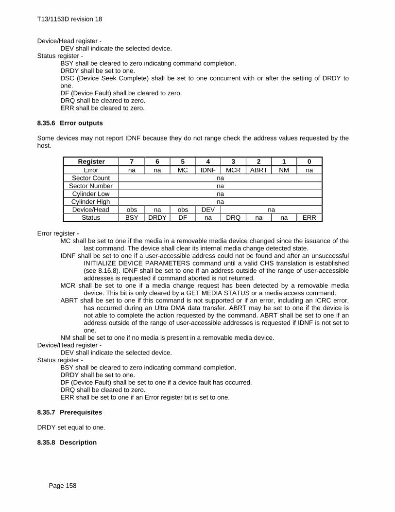
T13/1153D revision 18
Page 158
Device/Head register -DEV shall indicate the selected device.
Status register -BSY shall be cleared to zero indicating command completion.DRDY shall be set to one.DSC (Device Seek Complete) shall be set to one concurrent with or after the setting of DRDY toone.DF (Device Fault) shall be cleared to zero.DRQ shall be cleared to zero.ERR shall be cleared to zero.
8.35.6 Error outputs
Some devices may not report IDNF because they do not range check the address values requested by thehost.
Register 7 6 5 4 3 2 1 0Error na na MC IDNF MCR ABRT NM na
Sector Count naSector Number naCylinder Low naCylinder High naDevice/Head obs na obs DEV na
Status BSY DRDY DF na DRQ na na ERR
Error register -MC shall be set to one if the media in a removable media device changed since the issuance of the
last command. The device shall clear its internal media change detected state.IDNF shall be set to one if a user-accessible address could not be found and after an unsuccessful
INITIALIZE DEVICE PARAMETERS command until a valid CHS translation is established(see 8.16.8). IDNF shall be set to one if an address outside of the range of user-accessibleaddresses is requested if command aborted is not returned.
MCR shall be set to one if a media change request has been detected by a removable mediadevice. This bit is only cleared by a GET MEDIA STATUS or a media access command.
ABRT shall be set to one if this command is not supported or if an error, including an ICRC error,has occurred during an Ultra DMA data transfer. ABRT may be set to one if the device isnot able to complete the action requested by the command. ABRT shall be set to one if anaddress outside of the range of user-accessible addresses is requested if IDNF is not set toone.
NM shall be set to one if no media is present in a removable media device.Device/Head register -
DEV shall indicate the selected device.Status register -
BSY shall be cleared to zero indicating command completion.DRDY shall be set to one.DF (Device Fault) shall be set to one if a device fault has occurred.DRQ shall be cleared to zero.ERR shall be set to one if an Error register bit is set to one.
8.35.7 Prerequisites
DRDY set equal to one.
8.35.8 Description

T13/1153D revision 18
Page 159
This command allows the host to provide advanced notification that particular data may be requested by thehost in a subsequent command. DSC shall be set to one concurrent with or after the setting of DRDY to onewhen updating the Status register for this command.

T13/1153D revision 18
Page 160
8.36 SERVICE
8.36.1 Command code
A2h
8.36.2 Feature set
Overlap and Queued feature sets− Mandatory when the PACKET, Overlapped feature set is implemented.
8.36.3 Protocol
PACKET or READ/WRITE DMA QUEUED (see 9.11 and 9.12).
8.36.4 Inputs
Register 7 6 5 4 3 2 1 0Features na
Sector Count naSector Number naCylinder Low naCylinder High naDevice/Head obs na obs DEV na na na naCommand A2h
Device/Head register -DEV shall indicate the selected device.
8.36.5 Outputs
Outputs as a result of a SERVICE command are described in the command description for the command forwhich SERVICE is being requested.
8.36.6 Prerequisites
The device shall have performed a bus release for a previous overlap PACKET, READ DMA QUEUED, orWRITE DMA QUEUED command and shall have set the SERV bit to one to request the SERVICEcommand be issued to continue data transfer and/or provide command status (see 8.37.15).
8.36.7 Description
The SERVICE command is used to provide data transfer and/or status of a command that was previouslybus released.

T13/1153D revision 18
Page 161
8.37 SET FEATURES
8.37.1 Command code
EFh
8.37.2 Feature set
General feature set− Mandatory for all devices.− Set transfer mode subcommand is mandatory.− Enable/disable write cache subcommands are mandatory when a write cache is implemented.− Enable/Disable Media Status Notification sub commands are mandatory if the Removable
Media feature set is implemented.− All other subcommands are optional.
8.37.3 Protocol
Non-data (see 9.9).
8.37.4 Inputs
Table 19 defines the value of the subcommand in the Feature register. Some subcommands use otherregisters, such as the Sector Count register to pass additional information to the device.
Register 7 6 5 4 3 2 1 0Features Subcommand code
Sector Count Subcommand specificSector Number Subcommand specificCylinder Low Subcommand specificCylinder High Subcommand specificDevice/Head obs na obs DEV na na na naCommand EFh
Device/Head register -DEV shall indicate the selected device.
8.37.5 Normal outputs
See the subcommand descriptions.
8.37.6 Error outputs
If any subcommand input value is not supported or is invalid, the device shall return command aborted.
Register 7 6 5 4 3 2 1 0Error na na na na na ABRT na na
Sector Count naSector Number naCylinder Low naCylinder High naDevice/Head obs na obs DEV na
Status BSY DRDY DF na DRQ na na ERR
T13/1153D revision 18
Page 162
Error register -ABRT shall be set to one if this subcommand is not supported or if value is invalid. ABRT may beset to one if the device is not able to complete the action requested by the command.
Device/Head register -DEV shall indicate the selected device.
Status register -BSY shall be cleared to zero indicating command completion.DRDY shall be set to one.DF (Device Fault) shall be set to one if a device fault has occurred.DRQ shall be cleared to zero.ERR shall be set to one if an Error register bit is set to one.
8.37.7 Prerequisites
DRDY shall be set to one.
8.37.8 Description
This command is used by the host to establish parameters that affect the execution of certain devicefeatures. Table 19 defines these features.
At power on, or after a hardware reset, the default setting of the functions specified by the subcommandsare vendor specific.

T13/1153D revision 18
Page 163
Table 19 −− SET FEATURES register definitionsValue
(see note)01h Retired02h Enable write cache03h Set transfer mode based on value in Sector Count register. Table 20 defines
values.04h Obsolete05h Enable advanced power management31h Disable Media Status Notification33h Obsolete44h Obsolete54h Obsolete55h Disable read look-ahead feature5Dh Enable release interrupt5Eh Enable SERVICE interrupt66h Disable reverting to power on defaults77h Obsolete81h Retired82h Disable write cache84h Obsolete85h Disable advanced power management88h Obsolete95h Enable Media Status Notification99h Obsolete9Ah ObsoleteAAh Enable read look-ahead featureABh ObsoleteBBh ObsoleteCCh Enable reverting to power on defaultsDDh Disable release interruptDEh Disable SERVICE interrupt
NOTE − All values not shown are reserved for future definition.
8.37.9 Enable/disable write cache
Subcommand codes 02h and 82h allow the host to enable or disable write cache in devices that implementwrite cache. When the subcommand disable write cache is issued, the device shall initiate the sequence toflush cache to non-volatile memory before command completion (see 8.10).
8.37.10 Set transfer mode
A host selects the transfer mechanism by Set Transfer Mode, subcommand code 03h, and specifying avalue in the Sector Count register. The upper 5 bits define the type of transfer and the low order 3 bitsencode the mode value. One PIO mode and one DMA mode shall be selected at all times. The host maychange the selected modes by the SET FEATURES command.

T13/1153D revision 18
Page 164
Table 20 −− Transfer mode values Mode Bits (7:3) Bits (2:0)
PIO default mode 00000b 000bPIO default mode, disable IORDY 00000b 001bPIO flow control transfer mode 00001b modeRetired 00010b naMultiword DMA mode 00100b modeUltra DMA mode 01000b modeReserved 10000b namode = transfer mode number
If a device supports this standard, and receives a SET FEATURES command with a Set Transfer Modeparameter and a Sector Count register value of “00000000b”, it shall set its default PIO mode. If the valueis “00000001b” and the device supports disabling of IORDY, then the device shall set its default PIO modeand disable IORDY. A device shall support all PIO modes below the highest mode supported, e.g., if PIOmode 1 is supported PIO mode 0 shall be supported.
Support of IORDY is mandatory when PIO mode 3 or above is the current mode of operation.
Devices reporting support for Multi Word DMA mode 1 shall also support Multi Word DMA mode 0. A deviceshall support all Multi Word DMA modes below the highest mode supported, e.g., if Multi Word DMA mode1 is supported Multi Word DMA mode 0 shall be supported.
A device shall support all Ultra DMA modes below the highest mode supported, e.g., if Ultra DMA mode 1 issupported Ultra DMA mode 0 shall be supported.
If an Ultra DMA mode is enabled any previously enabled Multi Word DMA mode shall be disabled by thedevice. If a Multiword DMA mode is enabled any previously enabled Ultra DMA mode shall be disabled bythe device.
8.37.11 Enable/disable advanced power management
Subcommand code 05h allows the host to enable Advanced Power Management. To enable AdvancedPower Management, the host writes the Sector Count register with the desired advanced powermanagement level and then executes a SET FEATURES command with subcommand code 05h. Thepower management level is a scale from the lowest power consumption setting of 01h to the maximumperformance level of FEh. Table 21 shows these values.
Table 21 −− Advanced power management levelsLevel Sector Count value
Maximum performance FEhIntermediate power management levels without Standby 81h-FDhMinimum power consumption without Standby 80hIntermediate power management levels with Standby 02h-7FhMinimum power consumption with Standby 01hReserved FFhReserved 00h
Device performance may increase with increasing power management levels. Device power consumptionmay increase with increasing power management levels. The power management levels may containdiscrete bands. For example, a device may implement one power management method from 80h to A0hand a higher performance, higher power consumption method from level A1h to FEh. Advanced powermanagement levels 80h and higher do not permit the device to spin down to save power.
Subcommand code 85h disables Advanced Power Management. Subcommand 85h may not beimplemented on all devices that implement SET FEATURES subcommand 05h.
T13/1153D revision 18
Page 165
8.37.12 Enable/disable Media Status Notification
Subcommand code 31h disables Media Status Notification and leaves the media in an unlocked state. IfMedia Status Notification is disabled when this subcommand is received, the subcommand has no effect.
Subcommand code 95h enables Media Status Notification and clears any previous media lock state. Thissubcommand returns the device capabilities for media eject, media lock, previous state of Media StatusNotification and the current version of Media Status Notification supported in the Cylinder Low and CylinderHigh registers as described below.
Register 7 6 5 4 3 2 1 0Cylinder Low VERCylinder High r r r r r PEJ LOCK PENA
Cylinder Low register -VER shall contain the Media Status Notification version supported by the device (currently 0x00h)
Cylinder High register -PENA shall be set to one if Media Status Notification was enabled prior to the receipt of this
command,LOCK shall be set to one if the device is capable of locking the media preventing manual ejection.PEJ shall be set to one if the device has a power eject mechanism that is capable of physically
ejecting the media when a MEDIA EJECT command is sent to the device. This bit must be setto zero if the device only unlocks the media when it receives a MEDIA EJECT command.
r (reserved) shall be cleared to zero.
8.37.13 Enable/disable read look-ahead
Subcommand codes AAh and 55h allow the host to request the device to enable or disable read look-ahead.Error recovery performed by the device is vendor specific.
8.37.14 Enable/disable release interrupt
Subcommand codes 5Dh and DDh allow a host to enable or disable the asserting INTRQ if nIEN is clearedto zero when a device releases the bus for an overlapped PACKET command.
8.37.15 Enable/disable SERVICE interrupt
Subcommand codes 5Eh and DEh allow a host to enable or disable the asserting of an interrupt when DRQis set to one in response to a SERVICE command.
8.37.16 Enable/disable reverting to defaults
Subcommand codes CCh and 66h allow the host to enable or disable the device from reverting to power ondefault values. A setting of 66h allows settings that may have been modified since power on to remain at thesame setting after a software reset.

T13/1153D revision 18
Page 166
8.38 SET MAX ADDRESS
8.38.1 Command code
F9h
8.38.2 Feature set
Host Protected Area feature set.− Mandatory when the Host Protected Area feature set is implemented.− Use prohibited when the Removable feature set is implemented.
8.38.3 Protocol
Non-data command (see 9.9).
8.38.4 Inputs
Register 7 6 5 4 3 2 1 0Features na
Sector Count na V VSector Number Native max address sector number or set max
LBACylinder Low Set max cylinder low or LBACylinder High Set max cylinder high or LBADevice/Head obs LBA obs DEV Native max address
head number or setmax LBA
Command F9h
Sector Count -V V (Value volatile). If bit 0 is set to one, the device shall preserve the maximum values over power-up or hardware reset. If bit 0 is cleared to zero, the device shall revert to the most recent non-volatile maximum address value setting over power-up or hardware reset.
Sector Number -contains the native max address sector number (IDENTIFY DEVICE word 6) or LBA bits (7:0) value
to be set.Cylinder Low -
contains the maximum cylinder low or LBA bits (15:8) value to be set.Cylinder High -
contains the maximum cylinder high or LBA bits (23:16) value to be set.Device/Head -
if LBA is set to one, the maximum address value is an LBA value.If LBA is cleared to zero, the maximum address value is a CHS value.DEV shall indicate the selected device.Bits (3:0) contain the native max address head number (IDENTIFY DEVICE word 3 minus one) orLBA bits (27:24) value to be set.

T13/1153D revision 18
Page 167
8.38.5 Normal outputs
Register 7 6 5 4 3 2 1 0Error na
Sector Count naSector Number Native max sector number or max LBACylinder Low Max cylinder low or LBACylinder High Max cylinder high or LBADevice/Head obs na obs DEV Native max head or max LBA
Status BSY DRDY DF na DRQ na na ERR
Sector Number -maximum native sector number or LBA bits (7:0) set on the device.
Cylinder Low -maximum cylinder number low or LBA bits (15:8) set on the device.
Cylinder High -maximum cylinder number high or LBA bits (23:16) set on device.
Device/Head -DEV shall indicate the selected device.maximum native head number or LBA bits (27:24) set on the device.
Status register -BSY shall be cleared to zero indicating command completion.DRDY shall be set to one.DF (Device Fault) shall be cleared to zero.DRQ shall be cleared to zero.ERR shall be cleared to zero.
8.38.6 Error outputs
If this command is not supported or the maximum value to be set exceeds the capacity of the device, thedevice shall return command aborted.
Register 7 6 5 4 3 2 1 0Error na na na IDNF na ABRT na na
Sector Count naSector Number naCylinder Low naCylinder High naDevice/Head obs na obs DEV na
Status BSY DRDY na na na na na ERR
Error register -ABRT shall be set to one if this command is not supported, maximum value requested exceeds the
device capacity, the set max cylinder number is greater than 16,383, or the command is notimmediately preceded by a READ NATIVE MAX ADDRESS command. ABRT may be set toone if the device is not able to complete the action requested by the command.
IDNF shall be set to one if the command was the second non-volatile SET MAX ADDRESScommand after power on or hardware reset.
Device/Head register -DEV shall indicate the selected device.
Status register -BSY shall be cleared to zero indicating command completion.DRDY shall be set to one.ERR shall be set to one if an Error register bit is set to one.

T13/1153D revision 18
Page 168
8.38.7 Prerequisites
DRDY set equal to one. A successful READ NATIVE MAX ADDRESS command shall immediately precedea SET MAX ADDRESS command.
8.38.8 Description
This command allows the host to redefine the maximum address of the user-accessible address space ineither LBA translation or the current CHS translation. The host may either set a new maximum cylindernumber for CHS translation or a new maximum LBA address for LBA translation. After a successful SETMAX ADDRESS command using a new maximum cylinder number value the content of all IDENTIFYDEVICE words shall comply with 6.2.1 in addition to the following:1) The content of words 3, 6, 55, and 56 are unchanged2) The content of word 1 shall equal (the new Set max cylinder number + 1) or 16,383, whichever is less3) The content of words (61:60) shall equal [(the new content of word 1 as determined by the successful
SET MAX ADDRESS command) * (the content of word 3) * (the content of word 6)]4) If the content of words (61:60) as determined by a successful SET MAX ADDRESS command is less
than 16,514,064, then the content of word 54 shall be equal to [(the content of words (61:60)) ÷ ((thecontent of IDENTIFY DEVICE word 55) * (the content of word 56)] or 65,535, whichever is less
5) If the content of word (61:60) as determined by a successful SET MAX ADDRESS command is greaterthan 16,514,064, then word 54 shall equal the whole number result of [[(16,514,064) ÷ [(the content ofword 55) * (the content of word 56)]] or 65,535 whichever is less) The content of words (58:57) shallbe equal to [(the new content of word 54 as determined by the successful SET MAX ADDRESScommand) * (the content of word 55) * (the content of word 56)]
After a successful SET MAX ADDRESS command using a new maximum LBA address the content of allIDENTIFY DEVICE words shall comply with 6.2.1 in addition to the following:− The content of words (61:60) shall be equal to the new Maximum LBA address + 1.− If the content of words (61:60) is greater than 16,514,064 and if the device does not support CHS
addressing, then the content of words 1, 3, 6, 54, 55, 56, and (58:57) shall equal zero.
If the device supports CHS addressing:− The content of words 3, 6, 55, and 56 are unchanged.− If the new content of words (61:60) is less than 16,514,064, then the content of word 1 shall be equal to
[(the new content of words (61:60)) ÷ [(the content of word 3) * (the content of word 6)]] or 65,535,whichever is less.
− If the new content of words (61:60) is greater than or equal to 16,514,064, then the content of word 1shall be equal to 16,383.
− If the new content of words (61:60) is less than 16,514,064, then the content of word 54 shall be equal to[(the new content of words (61:60)) ÷ [(the content of word 55) * (the content of word 56)]].
− If the new content of words (61:60) is greater than or equal to 16,514,064, then the content of word 54shall be equal to 16,383.
− Words (58:57) shall be equal to [(the content of word 54) * (the content of word 55) * (the content ofword 56).
After successful command completion, all read and write access attempts to addresses greater thanspecified by the successful SET MAX ADDRESS command shall be rejected with an “ID Not Found” error.
Hosts should not issue more than one non-volatile SET MAX ADDRESS command after a power on orhardware reset. Devices shall report an “ID Not Found” error upon receiving a second non-volatile SETMAX ADDRESS command after a power on or hardware reset.
The contents of IDENTIFY DEVICE words shall not be changed if a SET MAX ADDRESS command fails forany reason.

T13/1153D revision 18
Page 169
8.39 SET MULTIPLE MODE
8.39.1 Command code
C6h
8.39.2 Feature set
General feature setMandatory for devices not implementing the PACKET Command feature set.Use prohibited for devices implementing the PACKET Command feature set.
8.39.3 Protocol
Non-data (see 9.9).
8.39.4 Inputs
The Sector Count register contains number of sectors per block to use on all following READ/WRITEMULTIPLE commands. The host shall set Sector Count values equal to 2, 4, 8, 16, 32, 64, or 128.
Register 7 6 5 4 3 2 1 0Features na
Sector Count Sectors per blockSector Number naCylinder Low naCylinder High naDevice/Head obs na obs DEV na na na naCommand C6h
Device/Head register -DEV shall indicate the selected device.
8.39.5 Normal outputs
Register 7 6 5 4 3 2 1 0Error na
Sector Count naSector Number naCylinder Low naCylinder High naDevice/Head obs na obs DEV na na na na
Status BSY DRDY DF na DRQ na na ERR
Device/Head register -DEV shall indicate the selected device.
Status register -BSY shall be cleared to zero indicating command completion.DRDY shall be set to one.DF (Device Fault) shall be cleared to zero.DRQ shall be cleared to zero.ERR shall be cleared to zero.

T13/1153D revision 18
Page 170
8.39.6 Error outputs
If a block count is not supported, the device shall return command aborted.
Register 7 6 5 4 3 2 1 0Error na na na na na ABRT na na
Sector Count naSector Number naCylinder Low naCylinder High naDevice/Head obs na obs DEV na
Status BSY DRDY DF na DRQ na na ERR
Error register -ABRT shall be set to one if the block count is not supported. ABRT may be set to one if the deviceis not able to complete the action requested by the command.
Device/Head register -DEV shall indicate the selected device.
Status register -BSY shall be cleared to zero indicating command completion.DRDY shall be set to one.DF (Device Fault) shall be set to one if a device fault has occurred.DRQ shall be cleared to zero.ERR shall be set to one if an Error register bit is set to one.
8.39.7 Prerequisites
DRDY set equal to one.
8.39.8 Description
This command establishes the block count for READ MULTIPLE and WRITE MULTIPLE commands.
Devices shall support the block size specified in the IDENTIFY DEVICE parameter word 47, bits 7 through0, and may also support smaller values.
Upon receipt of the command, the device checks the Sector Count register. If the Sector Count registercontains a valid value and the block count is supported, the value is used for all subsequent READMULTIPLE and WRITE MULTIPLE commands and their execution is enabled.
T13/1153D revision 18
Page 171
8.40 SLEEP
8.40.1 Command code
E6h
8.40.2 Feature set
Power Management feature set.− Power Management feature set is mandatory when power management is not implemented by a
PACKET power management feature set.− This command is mandatory when the Power Management feature set is implemented.
8.40.3 Protocol
Non-data command (see 9.9).
8.40.4 Inputs
Register 7 6 5 4 3 2 1 0Features na
Sector Count naSector Number naCylinder Low naCylinder High naDevice/Head obs na obs DEV na na na naCommand E6h
Device/Head register -DEV shall indicate the selected device.
8.40.5 Normal outputs
Register 7 6 5 4 3 2 1 0Error na
Sector Count naSector Number naCylinder Low naCylinder High naDevice/Head obs na obs DEV na na na na
Status BSY DRDY DF na DRQ na na ERR
Device/Head register -DEV shall indicate the selected device.
Status register -BSY shall be cleared to zero indicating command completion.DRDY shall be set to one.DF (Device Fault) shall be cleared to zero.DRQ shall be cleared to zero.ERR shall be cleared to zero.

T13/1153D revision 18
Page 172
8.40.6 Error outputs
The device shall return command aborted if the device does not support the Power Management featureset.
Register 7 6 5 4 3 2 1 0Error na na na na na ABRT na na
Sector Count naSector Number naCylinder Low naCylinder High naDevice/Head obs na obs DEV na
Status BSY DRDY DF na DRQ na na ERR
Error register -ABRT shall be set to one if the device does not support the Power Management feature set. ABRT
may be set to one if the device is not able to complete the action requested by thecommand.
Device/Head register -DEV shall indicate the selected device.
Status register -BSY shall be cleared to zero indicating command completion.DRDY shall be set to one.DF (Device Fault) shall be set to one if a device fault has occurred.DRQ shall be cleared to zero.ERR shall be set to one if an Error register bit is set to one.
8.40.7 Prerequisites
DRDY set equal to one.
8.40.8 Description
This command is the only way to cause the device to enter Sleep mode.
This command causes the device to set the BSY bit to one, prepare to enter Sleep mode, clear the BSY bitto zero and assert INTRQ. The host shall read the Status register in order to clear the interrupt and allowthe device to enter Sleep mode. In Sleep mode, the device only responds to the assertion of the RESETsignal and the writing of the SRST bit in the Device Control register and releases its driven signal lines. Thehost shall not attempt to access the Command Block registers while the device is in Sleep mode.
Because some host systems may not read the Status register and clear the interrupt, a device mayautomatically release INTRQ and enter Sleep mode after a vendor specific time period of not less than 2 s.
The only way to recover from Sleep mode is with a software reset, a hardware reset, or a DEVICE RESETcommand.
A device shall not power on in Sleep mode nor remain in Sleep mode following a reset sequence.

T13/1153D revision 18
Page 173
8.41 SMART
Individual SMART commands are identified by the value placed in the Feature register. Table 22 showsthese Feature register values.
Table 22 −− SMART Feature register valuesValue Command
00h-CFh reservedD0h SMART READ DATAD1h obsoleteD2h SMART ENABLE/DISABLE ATTRIBUTE AUTOSAVED3h SMART SAVE ATTRIBUTE VALUESD4h SMART EXECUTE OFF-LINE IMMEDIATE
D5h-D6h reservedD7h obsoleteD8h SMART ENABLE OPERATIONSD9h SMART DISABLE OPERATIONSDAh SMART RETURN STATUSDBh obsolete
DCh-DFh reservedE0h-FFh vendor specific

T13/1153D revision 18
Page 174
8.41.1 SMART DISABLE OPERATIONS
8.41.1.1 Command code
B0h with a Feature register value of D9h.
8.41.1.2 Feature set
SMART feature set.− Mandatory when the SMART feature set is implemented.− Use prohibited when the PACKET Command feature set is implemented.
8.41.1.3 Protocol
Non-data command (see 9.9).
8.41.1.4 Inputs
The Features register shall be set to D9h. The Cylinder Low register shall be set to 4Fh. The Cylinder Highregister shall be set to C2h.
Register 7 6 5 4 3 2 1 0Features D9h
Sector Count naSector Number naCylinder Low 4FhCylinder High C2hDevice/Head obs na obs DEV na na na naCommand B0h
Device/Head register -DEV shall indicate the selected device.
8.41.1.5 Normal outputs
Register 7 6 5 4 3 2 1 0Error na
Sector Count naSector Number naCylinder Low naCylinder High naDevice/Head obs na obs DEV na na na na
Status BSY DRDY DF na DRQ na na ERR
Device/Head register -DEV shall indicate the selected device.
Status register -BSY shall be cleared to zero indicating command completion.DRDY shall be set to one.DF (Device Fault) shall be cleared to zero.DRQ shall be cleared to zero.ERR shall be cleared to zero.

T13/1153D revision 18
Page 175
8.41.1.6 Error outputs
If the device does not support this command, if SMART is not enabled, or if the values in the Features,Cylinder Low, or Cylinder High registers are invalid, the device shall return command aborted.
Register 7 6 5 4 3 2 1 0Error na na na na na ABRT na na
Sector Count naSector Number naCylinder Low naCylinder High naDevice/Head obs na obs DEV na
Status BSY DRDY DF na DRQ na na ERR
Error register -ABRT shall be set to one if this command is not supported, if SMART is not enabled, or if input
register values are invalid. ABRT may be set to one if the device is not able to complete theaction requested by the command.
Device/Head register -DEV shall indicate the selected device.
Status register -BSY shall be cleared to zero indicating command completion.DRDY shall be set to one.DF (Device Fault) shall be set to one if a device fault has occurred.DRQ shall be cleared to zero.ERR shall be set to one if an Error register bit is set to one.
8.41.1.7 Prerequisites
DRDY set equal to one. SMART enabled.
8.41.1.8 Description
This command disables all SMART capabilities within the device including any and all timer and event countfunctions related exclusively to this feature. After receipt of this command the device shall disable allSMART operations. SMART data shall no longer be monitored or saved by the device. The state of SMART(either enabled or disabled) shall be preserved by the device across power cycles.
After receipt of this command by the device, all other SMART commands (including SMART DISABLEOPERATIONS commands), with the exception of SMART ENABLE OPERATIONS, are disabled and invalidand shall be command aborted by the device.
T13/1153D revision 18
Page 176
8.41.2 SMART ENABLE/DISABLE ATTRIBUTE AUTOSAVE
8.41.2.1 Command code
B0h with a Feature register value of D2h.
8.41.2.2 Feature set
SMART feature set.− Mandatory when the SMART feature set is implemented.− Use prohibited when the PACKET Command feature set is implemented.
8.41.2.3 Protocol
Non-data command (see 9.9).
8.41.2.4 Inputs
The Features register shall be set to D2h. The Cylinder Low register shall be set to 4Fh. The Cylinder Highregister shall be set to C2h. The Sector Count register is set to 00h to disable attribute autosave and a valueof F1h is set to enable attribute autosave.
Register 7 6 5 4 3 2 1 0Features D2h
Sector Count 00h or F1hSector Number naCylinder Low 4FhCylinder High C2hDevice/Head obs na obs DEV na na na naCommand B0h
Device/Head register -DEV shall indicate the selected device.
8.41.2.5 Normal outputsRegister 7 6 5 4 3 2 1 0
Error naSector Count na
Sector Number naCylinder Low naCylinder High naDevice/Head obs na obs DEV na na na na
Status BSY DRDY DF na DRQ na na ERR
Device/Head register -DEV shall indicate the selected device.
Status register -BSY shall be cleared to zero indicating command completion.DRDY shall be set to one.DF (Device Fault) shall be cleared to zero.DRQ shall be cleared to zero.ERR shall be cleared to zero.
T13/1153D revision 18
Page 177
8.41.2.6 Error outputs
If the device does not support this command, if SMART is disabled, or if the values in the Features, CylinderLow, or Cylinder High registers are invalid, the device shall return command aborted.
Register 7 6 5 4 3 2 1 0Error na na na na na ABRT na na
Sector Count naSector Number naCylinder Low naCylinder High naDevice/Head obs na obs DEV na
Status BSY DRDY DF na DRQ na na ERR
Error register -ABRT shall be set to one if this command is not supported, if SMART is disabled, or if the input
register values are invalid. ABRT may be set to one if the device is not able to complete theaction requested by the command.
Device/Head register -DEV shall indicate the selected device.
Status register -BSY shall be cleared to zero indicating command completion.DRDY shall be set to one.DF (Device Fault) shall be set to one if a device fault has occurred.DRQ shall be cleared to zero.ERR shall be set to one if an Error register bit is set to one.
8.41.2.7 Prerequisites
DRDY set equal to one. SMART enabled.
8.41.2.8 Description
This command enables and disables the optional attribute autosave feature of the device. Depending uponthe implementation, this command may either allow the device, after some vendor specified event, toautomatically save its updated attribute values to non-volatile memory; or this command may cause theautosave feature to be disabled. The state of the attribute autosave feature (either enabled or disabled) shallbe preserved by the device across power cycles.
A value of zero written by the host into the device’s Sector Count register before issuing this command shallcause this feature to be disabled. Disabling this feature does not preclude the device from saving SMARTdata to non-volatile memory during some other normal operation such as during a power-on or power-offsequence or during an error recovery sequence.
A value of F1h written by the host into the device’s Sector Count register before issuing this command shallcause this feature to be enabled. Any other meaning of this value or any other non-zero value written by thehost into this register before issuing this command may differ from device to device. The meaning of anynon-zero value written to this register at this time shall be preserved by the device across power cycles.
If this command is not supported by the device, the device shall return command aborted upon receipt fromthe host.
During execution of the autosave routine the device shall not set BSY to one nor clear DRDY to zero. If thedevice receives a command from the host while executing its autosave routine it shall respond to the hostwithin two seconds.

T13/1153D revision 18
Page 178
8.41.3 SMART ENABLE OPERATIONS
8.41.3.1 Command code
B0h with a Feature register value of D8h.
8.41.3.2 Feature set
SMART feature set.− Mandatory when the SMART feature set is implemented.− Use prohibited when the PACKET Command feature set is implemented.
8.41.3.3 Protocol
Non-data command (see 9.9).
8.41.3.4 Inputs
The Features register shall be set to D8h. The Cylinder Low register shall be set to 4Fh. The Cylinder Highregister shall be set to C2h.
Register 7 6 5 4 3 2 1 0Features D8h
Sector Count naSector Number naCylinder Low 4FhCylinder High C2hDevice/Head obs na obs DEV na na na naCommand B0h
Device/Head register -DEV shall indicate the selected device.
8.41.3.5 Normal outputs
Register 7 6 5 4 3 2 1 0Error na
Sector Count naSector Number naCylinder Low naCylinder High naDevice/Head obs na obs DEV na na na na
Status BSY DRDY DF na DRQ na na ERR
Device/Head register -DEV shall indicate the selected device.
Status register -BSY shall be cleared to zero indicating command completion.DRDY shall be set to one.DF (Device Fault) shall be cleared to zero.DRQ shall be cleared to zero.ERR shall be cleared to zero.

T13/1153D revision 18
Page 179
8.41.3.6 Error outputs
If the device does not support this command or if the values in the Features, Cylinder Low, or Cylinder Highregisters are invalid, the device shall return command aborted.
Register 7 6 5 4 3 2 1 0Error na na na na na ABRT na na
Sector Count naSector Number naCylinder Low naCylinder High naDevice/Head obs na obs DEV na
Status BSY DRDY DF na DRQ na na ERR
Error register -ABRT shall be set to one if this command is not supported or if the input register values are invalid.
ABRT may be set to one if the device is not able to complete the action requested by thecommand.
Device/Head register -DEV shall indicate the selected device.
Status register -BSY shall be cleared to zero indicating command completion.DRDY shall be set to one.DF (Device Fault) shall be set to one if a device fault has occurred.DRQ shall be cleared to zero.ERR shall be set to one if an Error register bit is set to one.
8.41.3.7 Prerequisites
DRDY set equal to one.
8.41.3.8 Description
This command enables access to all SMART capabilities within the device. Prior to receipt of this commandSMART data are neither monitored nor saved by the device. The state of SMART (either enabled ordisabled) shall be preserved by the device across power cycles. Once enabled, the receipt of subsequentSMART ENABLE OPERATIONS commands shall not affect any SMART data or functions.

T13/1153D revision 18
Page 180
8.41.4 SMART EXECUTE OFF-LINE IMMEDIATE
8.41.4.1 Command code
B0h with the content of the Features register equal to D4h
8.41.4.2 Feature set
SMART feature set.− Optional when the SMART feature set is implemented.− Use prohibited when the PACKET Command feature set is implemented.
8.41.4.3 Protocol
Non-data command (see 9.9).
8.41.4.4 Inputs
The Features register shall be set to D4h. The Cylinder Low register shall be set to 4Fh. The Cylinder Highregister shall be set to C2h.
Register 7 6 5 4 3 2 1 0Features D4h
Sector Count naSector Number naCylinder Low 4FhCylinder High C2hDevice/Head obs na obs DEV na
Command B0h
Device/Head register -DEV shall indicate the selected device.
8.41.4.5 Normal Outputs
Register 7 6 5 4 3 2 1 0Features na
Sector Count naSector Number naCylinder Low naCylinder High naDevice/Head obs na obs DEV na
Status BSY DRDY DF na DRQ na na ERR
Device/Head register -DEV shall indicate the selected device.
Status register -BSY shall be cleared to zero indicating command completion.DRDY shall be set to one indicating that the device is capable of receiving any command.DF (Device Fault) shall be cleared to zero.DRQ shall be cleared to zero.ERR shall be cleared to zero.

T13/1153D revision 18
Page 181
8.41.4.6 Error Outputs
If the device does not support this command, if SMART is disabled, or if the values in the Features, CylinderLow, or Cylinder High registers are invalid, the device shall return command aborted.
Register 7 6 5 4 3 2 1 0Error na na na IDNF na ABRT na obs
Sector Count naSector Number naCylinder Low naCylinder High naDevice/Head obs na obs DEV na
Status BSY DRDY DF na DRQ na na ERR
Error register -IDNF shall be set to one if SMART data sector’s ID field could not be found.ABRT shall be set to one if this command is not supported, if SMART is not enabled, or if register
values are invalid. ABRT may be set to one if the device is not able to complete the actionrequested by the command.
Device/Head register -DEV shall indicate the selected device.
Status register -BSY shall be cleared to zero indicating command completion.DRDY shall be set to one indicating that the device is capable of receiving any command.DF (Device Fault) shall be set to one indicating that a device fault has occurred.DRQ shall be cleared to zero indicating that there is no data to be transferred.ERR shall be set to one if any Error register bit is set to one.
8.41.4.7 Prerequisites
DRDY set to one. SMART enabled.
8.41.4.8 Description
This command causes the device to immediately initiate the optional set of activities that collect SMARTdata in an off-line mode and then save this data to the device's non-volatile memory.
During execution of its off-line activities the device shall not set BSY nor clear DRDY.
If the device is in the process of performing its set of off-line data collection activities as a result of receivinga SMART EXECUTE OFF-LINE IMMEDIATE command from the host and is interrupted by any newcommand from the host except a SMART DISABLE OPERATIONS, SMART EXECUTE OFF-LINEIMMEDIATE, or STANDBY IMMEDIATE command, the device shall suspend or abort its off-line datacollection activities and service the host within two seconds after receipt of the new command. Afterservicing the interrupting command from the host the device may immediately re-initiate or resume its off-line data collection activities without any additional commands from the host (see the definition for Bit 2 inthe Off-line data collection capability byte in 8.41.5).
If the device is in the process of performing its off-line data collection activities and is interrupted by aSTANDBY IMMEDIATE command from the host, the device shall suspend or abort its off-line datacollection activities, and service the host within two seconds after receipt of the command. After receiving anew command that causes the device to exit a power saving mode, the device shall initiate or resume off-line data collection activities without any additional commands from the host unless these activities wereaborted by the device (see 8.41.5.8).
If the device is in the process of performing its off-line data collection activities and is interrupted by aSMART DISABLE OPERATIONS command from the host, the device shall suspend or abort its off-line data

T13/1153D revision 18
Page 182
collection activities and service the host within two seconds after receipt of the command. Upon receipt ofthe next SMART ENABLE OPERATIONS command the device may, after the next vendor specified event,either re-initiate its off-line data collection activities or resume those activities from where they had beenpreviously suspended.
If the device is in the process of performing its off-line data collection activities and is interrupted by aSMART EXECUTE OFF-LINE IMMEDIATE command from the host, the device shall abort its off-line datacollection activities and service the host within two seconds after receipt of the command. The device shallthen re-initiate its off-line data collection activities in response to the new EXECUTE OFF-LINE IMMEDIATEcommand.

T13/1153D revision 18
Page 183
8.41.5 SMART READ DATA
8.41.5.1 Command code
B0h with the content of the Features register equal to D0h.
8.41.5.2 Feature set
SMART feature set.− Optional when the SMART feature set is implemented.− Use prohibited when the PACKET Command feature set is implemented.
8.41.5.3 Protocol
PIO data in (see 9.7).
8.41.5.4 Inputs
The Features register shall be set to D0h. The Cylinder Low register shall be set to 4Fh. The Cylinder Highregister shall be set to C2h.
Register 7 6 5 4 3 2 1 0Features D0h
Sector Count naSector Number naCylinder Low 4FhCylinder High C2hDevice/Head obs na obs DEV na
Command B0h
Device/Head register -DEV shall indicate the selected device.
8.41.5.5 Normal outputs
Register 7 6 5 4 3 2 1 0Features na
Sector Count naSector Number naCylinder Low naCylinder High naDevice/Head obs na obs DEV na
Status BSY DRDY DF na DRQ na na ERR
Device/Head register -DEV shall indicate the selected device.
Status register -BSY shall be cleared to zero indicating command completion.DRDY shall be set to one indicating that the device is capable of receiving any command.DF (Device Fault) shall be cleared to zero.DRQ shall be cleared to zero.ERR shall be cleared to zero.

T13/1153D revision 18
Page 184
8.41.5.6 Error outputs
If the device does not support this command, if SMART is disabled, or if the values in the Features, CylinderLow, or Cylinder High registers are invalid, the device shall return command aborted.
Register 7 6 5 4 3 2 1 0Error na UNC na IDNF na ABRT na obs
Sector Count naSector Number naCylinder Low naCylinder High naDevice/Head obs na obs DEV na
Status BSY DRDY DF na DRQ na na ERR
Error register -UNC shall be set to one if SMART data is uncorrectable.IDNF shall be set to one if SMART data sector’s ID field could not be found or data structure
checksum occurred.ABRT shall be set to one if this command is not supported, if SMART is not enabled, or if register
values are invalid. ABRT may be set to one if the device is not able to complete the actionrequested by the command.
Device/Head register -DEV shall indicate the selected device.
Status register -BSY shall be cleared to zero indicating command completion.DRDY shall be set to one indicating that the device is capable of receiving any command.DF (Device Fault) shall be set to one indicating that a device fault has occurred.DRQ shall be cleared to zero indicating that there is no data to be transferred.ERR shall be set to one if any Error register bit is set to one.
8.41.5.7 Prerequisites
DRDY set to one. SMART enabled.
8.41.5.8 Description
This command returns the Device SMART data structure to the host.
Table 23 defines the 512 bytes that make up the Device SMART data structure. All multi-byte fields shownin this structure follow the byte ordering described in 3.2.7.

T13/1153D revision 18
Page 185
Table 23 −− Device SMART data structureByte F/V Descriptions0-361 X Vendor specific
362 V Off-line data collection status363 X Vendor specific
364-365 V Total time in seconds to complete off-line data collection activity366 X Vendor specific367 F Off-line data collection capability
368-369 F SMART capability370-385 R Reserved386-510 X Vendor specific
511 V Data structure checksumKey:F=the content of the byte is fixed and does not change.V=the content of the byte is variable and may change depending on the state of thedevice or the commands executed by the device.X=the content of the byte is vendor specific and may be fixed or variable.R=the content of the byte is reserved and shall be zero.
The value of the off-line data collection status byte defines the current status of the off-line activities of thedevice. Table 24 lists the values and their respective definitions.
Table 24 −− Off-line data collection status byte valuesValue Definition
00h or 80h Off-line data collection activity was never started.01h Reserved
02h or 82h Off-line data collection activity was completed without error.03h Reserved
04h or 84h Off-line data collection activity was suspended by an interrupting command fromhost.
05h or 85h Off-line data collection activity was aborted by an interrupting command from host.06h or 86h Off-line data collection activity was aborted by the device with a fatal error.07h-3Fh Reserved40h-7Fh Vendor specific
81h Reserved83h Reserved
87h-BFh ReservedC0h-FFh Vendor specific
The total time in seconds to complete off-line data collection activity word specifies how many seconds thedevice requires to complete its sequence of off-line data collection activity. Valid values for this word arefrom 0001h to FFFFh.
Off-line data collection capability.
The following describes the definition for the off-line data collection capability bits. If the value of all ofthese bits is equal to zero, then no off-line data collection is implemented by this device.
− − Bit 0 (EXECUTE OFF-LINE IMMEDIATE implemented bit) - If the value of this bit equals one, then theSMART EXECUTE OFF-LINE IMMEDIATE command is implemented by this device. If the value ofthis bit equals zero, then the SMART EXECUTE OFF-LINE IMMEDIATE command is not implementedby this device.
− Bit 1 (vendor specific).

T13/1153D revision 18
Page 186
− − Bit 2 (abort/restart off-line by host bit) - If the value of this bit equals one, then the device shall abort alloff-line data collection activity initiated by an SMART EXECUTE OFF-LINE IMMEDIATE commandupon receipt of a new command. Off-line data collection activity must be restarted by a new SMARTEXECUTE OFF-LINE IMMEDIATE command from the host. If the value of this bit equals zero, thedevice shall suspend off-line data collection activity after an interrupting command and resume off-linedata collection activity after some vendor-specified event.
− − Bits 3-7 (reserved).
SMART capability
The following describes the definition for the SMART capabilities bits. If the value of all of these bits isequal to zero, then automatic saving of SMART data is not implemented by this device.
− − Bit 0 (power mode SMART data saving capability bit) - If the value of this bit equals one, the deviceshall save its SMART data prior to going into a power saving mode (Idle, Standby, or Sleep) orimmediately upon return to Active or Idle mode from a Standby mode. If the value of this bit equalszero, the device shall not save its SMART data prior to going into a power saving mode (Idle, Standby,or Sleep) or immediately upon return to Active or Idle mode from a Standby mode.
− − Bit 1 (SMART data autosave after event capability bit) - The value of this bit shall be equal to one for
devices complying with this standard. − − Bits 2-15 (reserved).
The data structure checksum is the two's compliment of the result of a simple eight-bit addition of the first511 bytes in the data structure.

T13/1153D revision 18
Page 187
8.41.6 SMART RETURN STATUS
8.41.6.1 Command code
B0h with a Feature register value of DAh.
8.41.6.2 Feature set
SMART feature set.− Mandatory when the SMART feature set is implemented.− Use prohibited when the PACKET Command feature set is implemented.
8.41.6.3 Protocol
Non-data command (see 9.9).
8.41.6.4 Inputs
The Features register shall be set to DAh. The Cylinder Low register shall be set to 4Fh. The Cylinder Highregister shall be set to C2h.
Register 7 6 5 4 3 2 1 0Features DAh
Sector Count naSector Number naCylinder Low 4FhCylinder High C2hDevice/Head obs na obs DEV na na na naCommand B0h
Device/Head register -DEV shall indicate the selected device.
8.41.6.5 Normal outputs
If the device has not detected a threshold exceeded condition, the device sets the Cylinder Low register to4Fh and the Cylinder High register to C2h. If the device has detected a threshold exceeded condition, thedevice sets the Cylinder Low register to F4h and the Cylinder High register to 2Ch.
Register 7 6 5 4 3 2 1 0Error na
Sector Count naSector Number naCylinder Low 4Fh or F4hCylinder High C2h or 2ChDevice/Head obs na obs DEV na na na na
Status BSY DRDY DF na DRQ na na ERR
Cylinder Low -4Fh if threshold not exceeded, F4h if threshold exceeded.
Cylinder High -C2h if threshold not exceeded, 2Ch if threshold exceeded.
Device/Head register -DEV shall indicate the selected device.

T13/1153D revision 18
Page 188
Status register -BSY shall be cleared to zero indicating command completion.DRDY shall be set to one.DF (Device Fault) shall be cleared to zero.DRQ shall be cleared to zero.ERR shall be cleared to zero.
8.41.6.6 Error outputs
If the device does not support this command, if SMART is disabled, or if the values in the Features, CylinderLow, or Cylinder High registers are invalid, the device shall return command aborted.
Register 7 6 5 4 3 2 1 0Error na na na na na ABRT na na
Sector Count naSector Number naCylinder Low naCylinder High naDevice/Head obs na obs DEV na
Status BSY DRDY DF na DRQ na na ERR
Error register -ABRT shall be set to one if this command is not supported, if SMART is disabled, or if the input
register values are invalid. ABRT may be set to one if the device is not able to complete theaction requested by the command.
Device/Head register -DEV shall indicate the selected device.
Status register -BSY shall be cleared to zero indicating command completion.DRDY shall be set to one.DF (Device Fault) shall be set to one if a device fault has occurred.DRQ shall be cleared to zero.ERR shall be set to one if an Error register bit is set to one.
8.41.6.7 Prerequisites
DRDY set equal to one. SMART enabled.
8.41.6.8 Description
This command is used to communicate the reliability status of the device to the host at the host’s request. Ifa threshold exceeded condition is not detected by the device, the device shall set the Cylinder Low registerto 4Fh and the Cylinder High register to C2h. If a threshold exceeded condition is detected by the device,the device shall set the Cylinder Low register to F4h and the Cylinder High register to 2Ch.
T13/1153D revision 18
Page 189
8.41.7 SMART SAVE ATTRIBUTE VALUES
8.41.7.1 Command code
B0h with a Feature register value of D3h.
8.41.7.2 Feature set
SMART feature set.− Optional and not recommended when the SMART feature set is implemented.− Use prohibited when the PACKET Command feature set is implemented.
8.41.7.3 Protocol
Non-data command (see 9.9).
8.41.7.4 Inputs
The Features register shall be set to D3h. The Cylinder Low register shall be set to 4Fh. The Cylinder Highregister shall be set to C2h.
Register 7 6 5 4 3 2 1 0Features D3h
Sector Count naSector Number naCylinder Low 4FhCylinder High C2hDevice/Head obs na obs DEV na na na naCommand B0h
Device/Head register -DEV shall indicate the selected device.
8.41.7.5 Normal outputs
Register 7 6 5 4 3 2 1 0Error na
Sector Count naSector Number naCylinder Low naCylinder High naDevice/Head obs na obs DEV na na na na
Status BSY DRDY DF na DRQ na na ERR
Device/Head register -DEV shall indicate the selected device.
Status register -BSY shall be cleared to zero indicating command completion.DRDY shall be set to one.DF (Device Fault) shall be cleared to zero.DRQ shall be cleared to zero.ERR shall be cleared to zero.

T13/1153D revision 18
Page 190
8.41.7.6 Error outputs
If the device does not support this command, if SMART is disabled, or if the values in the Features, CylinderLow, or Cylinder High registers are invalid, the device shall return command aborted.
Register 7 6 5 4 3 2 1 0Error na na na na na ABRT na na
Sector Count naSector Number naCylinder Low naCylinder High naDevice/Head obs na obs DEV na
Status BSY DRDY DF na DRQ na na ERR
Error register -ABRT shall be set to one if this command is not supported, if SMART is disabled, or if the input
register values are invalid. ABRT may be set to one if the device is not able to complete theaction requested by the command.
Device/Head register -DEV shall indicate the selected device.
Status register -BSY shall be cleared to zero indicating command completion.DRDY shall be set to one.DF (Device Fault) shall be set to one if a device fault has occurred.DRQ shall be cleared to zero..ERR shall be set to one if an Error register bit is set to one.
8.41.7.7 Prerequisites
DRDY set equal to one. SMART enabled.
8.41.7.8 Description
This command causes the device to immediately save any updated attribute values to the device’s non-volatile memory regardless of the state of the attribute autosave timer.

T13/1153D revision 18
Page 191
8.42 STANDBY
8.42.1 Command code
E2h
8.42.2 Feature set
Power Management feature set.− Power Management feature set is mandatory when power management is not implemented by a
PACKET power management feature set.− This command is mandatory when the Power Management feature set is implemented.
8.42.3 Protocol
Non-data command (see 9.9).
8.42.4 Inputs
The value in the Sector Count register when the STANDBY command is issued shall determine the timeperiod programmed into the Standby timer. Table 14 defines these values.
Register 7 6 5 4 3 2 1 0Features na
Sector Count Time period valueSector Number naCylinder Low naCylinder High naDevice/Head obs na obs DEV na na na naCommand E2h
Device/Head register -DEV shall indicate the selected device.
8.42.5 Normal outputs
Register 7 6 5 4 3 2 1 0Error na
Sector Count naSector Number naCylinder Low naCylinder High naDevice/Head obs na obs DEV na na na na
Status BSY DRDY DF na DRQ na na ERR
Device/Head register -DEV shall indicate the selected device.
Status register -BSY shall be cleared to zero indicating command completion.DRDY shall be set to one.DF (Device Fault) shall be cleared to zero.DRQ shall be cleared to zero.ERR shall be cleared to zero.
T13/1153D revision 18
Page 192
8.42.6 Error outputs
The device shall return command aborted if the device does not support the Power Management featureset.
Register 7 6 5 4 3 2 1 0Error na na na na na ABRT na na
Sector Count naSector Number naCylinder Low naCylinder High naDevice/Head obs na obs DEV na
Status BSY DRDY DF na DRQ na na ERR
Error register -ABRT shall be set to one if the Power Management feature set is not supported. ABRT may be setto one if the device is not able to complete the action requested by the command.
Device/Head register -DEV shall indicate the selected device.
Status register -BSY shall be cleared to zero indicating command completion.DRDY shall be set to one.DF (Device Fault) shall be set to one if a device fault has occurred.DRQ shall be cleared to zero.ERR shall be set to one if an Error register bit is set to one.
8.42.7 Prerequisites
DRDY set equal to one.
8.42.8 Description
This command causes the device to enter the Standby mode.
If the Sector Count register is non-zero then the Standby timer shall be enabled. The value in the SectorCount register shall be used to determine the time programmed into the Standby timer (see Table 14).
If the Sector Count register is zero then the Standby timer is disabled.

T13/1153D revision 18
Page 193
8.43 STANDBY IMMEDIATE
8.43.1 Command code
E0h
8.43.2 Feature set
Power Management feature set.− Power Management feature set is mandatory when power management is not implemented by a
PACKET power management feature set.− This command is mandatory when the Power Management feature set is implemented.
8.43.3 Protocol
Non-data command (see 9.9).
8.43.4 Inputs
Register 7 6 5 4 3 2 1 0Features na
Sector Count naSector Number naCylinder Low naCylinder High naDevice/Head obs na obs DEV na na na naCommand E0h
Device/Head register -DEV shall indicate the selected device.
8.43.5 Normal outputs
Register 7 6 5 4 3 2 1 0Error na
Sector Count naSector Number naCylinder Low naCylinder High naDevice/Head obs na obs DEV na na na na
Status BSY DRDY DF na DRQ na na ERR
Device/Head register -DEV shall indicate the selected device.
Status register -BSY shall be cleared to zero indicating command completion.DRDY shall be set to one.DF (Device Fault) shall be cleared to zero.DRQ shall be cleared to zero.ERR shall be cleared to zero.

T13/1153D revision 18
Page 194
8.43.6 Error outputs
The device shall return command aborted if the device does not support the Power Management featureset.
Register 7 6 5 4 3 2 1 0Error na na na na na ABRT na na
Sector Count naSector Number naCylinder Low naCylinder High naDevice/Head obs na obs DEV na
Status BSY DRDY DF na DRQ na na ERR
Error register -ABRT shall be set to one if the Power Management feature set is not supported. ABRT may be setto one if the device is not able to complete the action requested by the command.
Device/Head register -DEV shall indicate the selected device.
Status register -BSY shall be cleared to zero indicating command completion.DRDY shall be set to one.DF (Device Fault) shall be set to one if a device fault has occurred.DRQ shall be cleared to zero.ERR shall be set to one if an Error register bit is set to one.
8.43.7 Prerequisites
DRDY set equal to one.
8.43.8 Description
This command causes the device to immediately enter the Standby mode.
T13/1153D revision 18
Page 195
8.44 WRITE BUFFER
8.44.1 Command code
E8h
8.44.2 Feature set
General feature set− Optional for devices not implementing the PACKET Command feature set.− Use prohibited for devices implementing the PACKET Command feature set.
8.44.3 Protocol
PIO data out (see 9.8).
8.44.4 Inputs
Register 7 6 5 4 3 2 1 0Features na
Sector Count naSector Number naCylinder Low naCylinder High naDevice/Head obs na obs DEV na na na naCommand E8h
Device/Head register -DEV shall indicate the selected device.
8.44.5 Normal outputs
Register 7 6 5 4 3 2 1 0Error na
Sector Count naSector Number naCylinder Low naCylinder High naDevice/Head obs na obs DEV na na na na
Status BSY DRDY DF na DRQ na na ERR
Device/Head register -DEV shall indicate the selected device.
Status register -BSY shall be cleared to zero indicating command completion.DRDY shall be set to one.DF (Device Fault) shall be cleared to zero.DRQ shall be cleared to zero.ERR shall be cleared to zero.
8.44.6 Error outputs
The device shall return command aborted if the command is not supported.

T13/1153D revision 18
Page 196
Register 7 6 5 4 3 2 1 0Error na na na na na ABRT na na
Sector Count naSector Number naCylinder Low naCylinder High naDevice/Head obs na obs DEV na
Status BSY DRDY DF na DRQ na na ERR
Error register -ABRT shall be set to one if this command is not supported. ABRT may be set to one if the device is not able to complete the action requested by the command.
Device/Head register -DEV shall indicate the selected device.
Status register -BSY shall be cleared to zero indicating command completion.DRDY shall be set to one.DF (Device Fault) shall be set to one if a device fault has occurred.DRQ shall be cleared to zero.ERR shall be set to one if an Error register bit is set to one.
8.44.7 Prerequisites
DRDY set equal to one.
8.44.8 Description
This command enables the host to write the contents of one sector in the device’s buffer.
The READ BUFFER and WRITE BUFFER commands shall be synchronized within the device such thatsequential WRITE BUFFER and READ BUFFER commands access the same 512 bytes within the buffer.

T13/1153D revision 18
Page 197
8.45 WRITE DMA
8.45.1 Command code
CAh or CBh
NOTE − The host should not use the CBh value.
8.45.2 Feature set
General feature setMandatory for devices not implementing the PACKET Command feature set.Use prohibited for devices implementing the PACKET Command feature set.
8.45.3 Protocol
DMA (see 9.10).
8.45.4 Inputs
The Cylinder Low, Cylinder High, Device/Head, and Sector Number specify the starting sector address to bewritten. The Sector Count register specifies the number of sectors to be transferred.
Register 7 6 5 4 3 2 1 0Features na
Sector Count Sector countSector Number Sector number or LBACylinder Low Cylinder low or LBACylinder High Cylinder high or LBADevice/Head obs LBA obs DEV Head number or LBACommand CAh or CBh
Sector Count -number of sectors to be transferred. A value of 00h indicates that 256 sectors are to be transferred.
Sector Number -starting sector number or LBA address bits (7:0).
Cylinder Low -starting cylinder number bits (7:0) or LBA address bits (15:8).
Cylinder High -starting cylinder number bits (15:8) or LBA address bits (23:16).
Device/Head -bit 6 set to one if LBA address, cleared to zero if CHS address.DEV shall indicate the selected device.bits (3:0) starting head number or LBA address bits (27:24).
T13/1153D revision 18
Page 198
8.45.5 Normal outputs
Register 7 6 5 4 3 2 1 0Error na
Sector Count naSector Number naCylinder Low naCylinder High naDevice/Head obs na obs DEV na na na na
Status BSY DRDY DF na DRQ na na ERR
Device/Head register -DEV shall indicate the selected device.
Status register -BSY shall be cleared to zero indicating command completion.DRDY shall be set to one.DF (Device Fault) shall be cleared to zero.DRQ shall be cleared to zero.ERR shall be cleared to zero.
8.45.6 Error outputs
An unrecoverable error encountered during the execution of this command results in the termination of thecommand. The Command Block registers contain the address of the sector where the first unrecoverableerror occurred. The amount of data transferred is indeterminate.
Register 7 6 5 4 3 2 1 0Error ICRC WP MC IDNF MCR ABRT NM obs
Sector Count naSector Number Sector number or LBACylinder Low Cylinder low or LBACylinder High Cylinder high or LBADevice/Head obs na obs DEV Head number or LBA
Status BSY DRDY DF na DRQ na na ERR
Error register -ICRC shall be set to one if an interface CRC error has occurred during an Ultra DMA data transfer.
The content of this bit is not applicable for Multiword DMA transfers.WP shall be set to one if the media in a removable media device is write protected.MC shall be set to one if the media in a removable media device changed since the issuance of the
last command. The device shall clear its internal media change detected state.IDNF shall be set to one if a user-accessible address could not be found and after an unsuccessful
INITIALIZE DEVICE PARAMETERS command until a valid CHS translation is established(see 8.16.8). IDNF shall be set to one if an address outside of the range of user-accessibleaddresses is requested if command aborted is not returned.
MCR shall be set to one if a media change request has been detected by a removable mediadevice. This bit is only cleared by a GET MEDIA STATUS or a media access command.
ABRT shall be set to one if this command is not supported or if an error, including an ICRC error,has occurred during an Ultra DMA data transfer. ABRT may be set to one if the device isnot able to complete the action requested by the command. ABRT shall be set to one if anaddress outside of the range of user-accessible addresses is requested if IDNF is not set toone.
NM shall be set to one if no media is present in a removable media device.Sector Number, Cylinder Low, Cylinder High, Device/Head -
shall be written with address of first unrecoverable error.DEV shall indicate the selected device.
Status register -

T13/1153D revision 18
Page 199
BSY shall be cleared to zero indicating command completion.DRDY shall be set to one.DF (Device Fault) shall be set to one if a device fault has occurred.DRQ shall be cleared to zero.ERR shall be set to one if an Error register bit is set to one.
8.45.7 Prerequisites
DRDY set equal to one. The host shall initialize the DMA channel.
8.45.8 Description
The WRITE DMA command allows the host to write data using the DMA data transfer protocol.
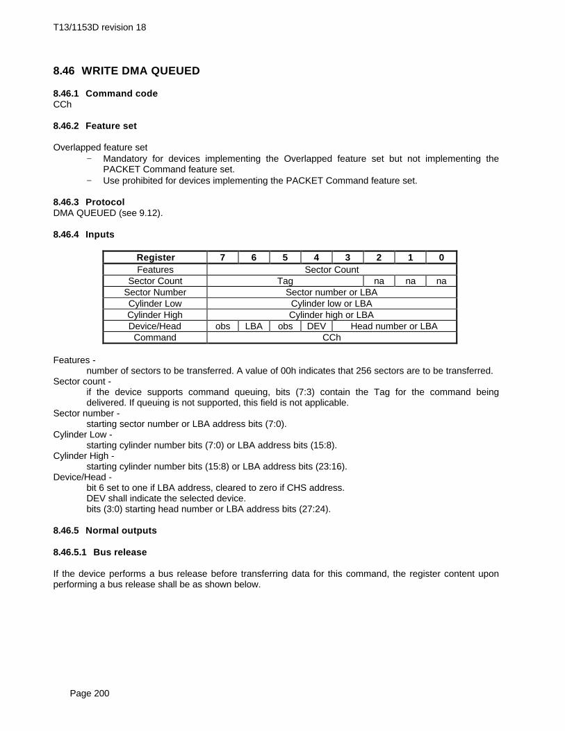
T13/1153D revision 18
Page 200
8.46 WRITE DMA QUEUED
8.46.1 Command codeCCh
8.46.2 Feature set
Overlapped feature set− Mandatory for devices implementing the Overlapped feature set but not implementing the
PACKET Command feature set.− Use prohibited for devices implementing the PACKET Command feature set.
8.46.3 ProtocolDMA QUEUED (see 9.12).
8.46.4 Inputs
Register 7 6 5 4 3 2 1 0Features Sector Count
Sector Count Tag na na naSector Number Sector number or LBACylinder Low Cylinder low or LBACylinder High Cylinder high or LBADevice/Head obs LBA obs DEV Head number or LBA
Command CCh
Features -number of sectors to be transferred. A value of 00h indicates that 256 sectors are to be transferred.
Sector count -if the device supports command queuing, bits (7:3) contain the Tag for the command beingdelivered. If queuing is not supported, this field is not applicable.
Sector number -starting sector number or LBA address bits (7:0).
Cylinder Low -starting cylinder number bits (7:0) or LBA address bits (15:8).
Cylinder High -starting cylinder number bits (15:8) or LBA address bits (23:16).
Device/Head -bit 6 set to one if LBA address, cleared to zero if CHS address.DEV shall indicate the selected device.bits (3:0) starting head number or LBA address bits (27:24).
8.46.5 Normal outputs
8.46.5.1 Bus release
If the device performs a bus release before transferring data for this command, the register content uponperforming a bus release shall be as shown below.
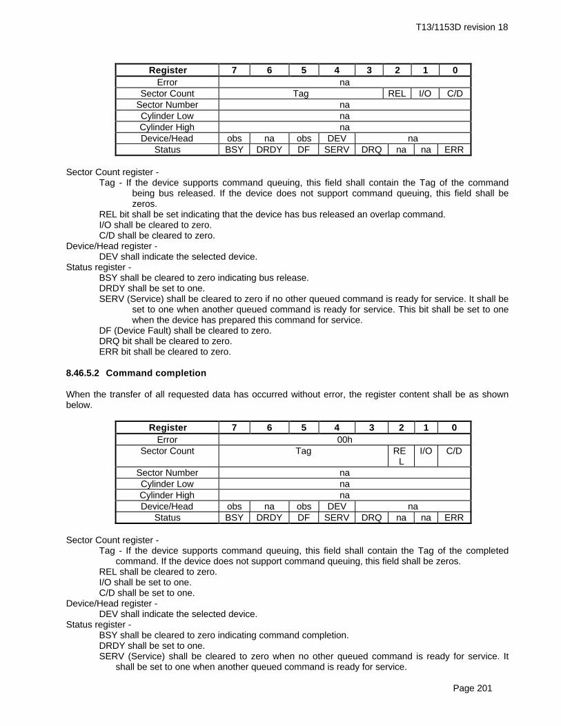
T13/1153D revision 18
Page 201
Register 7 6 5 4 3 2 1 0Error na
Sector Count Tag REL I/O C/DSector Number naCylinder Low naCylinder High naDevice/Head obs na obs DEV na
Status BSY DRDY DF SERV DRQ na na ERR
Sector Count register -Tag - If the device supports command queuing, this field shall contain the Tag of the command
being bus released. If the device does not support command queuing, this field shall bezeros.
REL bit shall be set indicating that the device has bus released an overlap command.I/O shall be cleared to zero.C/D shall be cleared to zero.
Device/Head register -DEV shall indicate the selected device.
Status register -BSY shall be cleared to zero indicating bus release.DRDY shall be set to one.SERV (Service) shall be cleared to zero if no other queued command is ready for service. It shall be
set to one when another queued command is ready for service. This bit shall be set to onewhen the device has prepared this command for service.
DF (Device Fault) shall be cleared to zero.DRQ bit shall be cleared to zero.ERR bit shall be cleared to zero.
8.46.5.2 Command completion
When the transfer of all requested data has occurred without error, the register content shall be as shownbelow.
Register 7 6 5 4 3 2 1 0Error 00h
Sector Count Tag REL
I/O C/D
Sector Number naCylinder Low naCylinder High naDevice/Head obs na obs DEV na
Status BSY DRDY DF SERV DRQ na na ERR
Sector Count register -Tag - If the device supports command queuing, this field shall contain the Tag of the completed
command. If the device does not support command queuing, this field shall be zeros.REL shall be cleared to zero.I/O shall be set to one.C/D shall be set to one.
Device/Head register -DEV shall indicate the selected device.
Status register -BSY shall be cleared to zero indicating command completion.DRDY shall be set to one.SERV (Service) shall be cleared to zero when no other queued command is ready for service. It
shall be set to one when another queued command is ready for service.
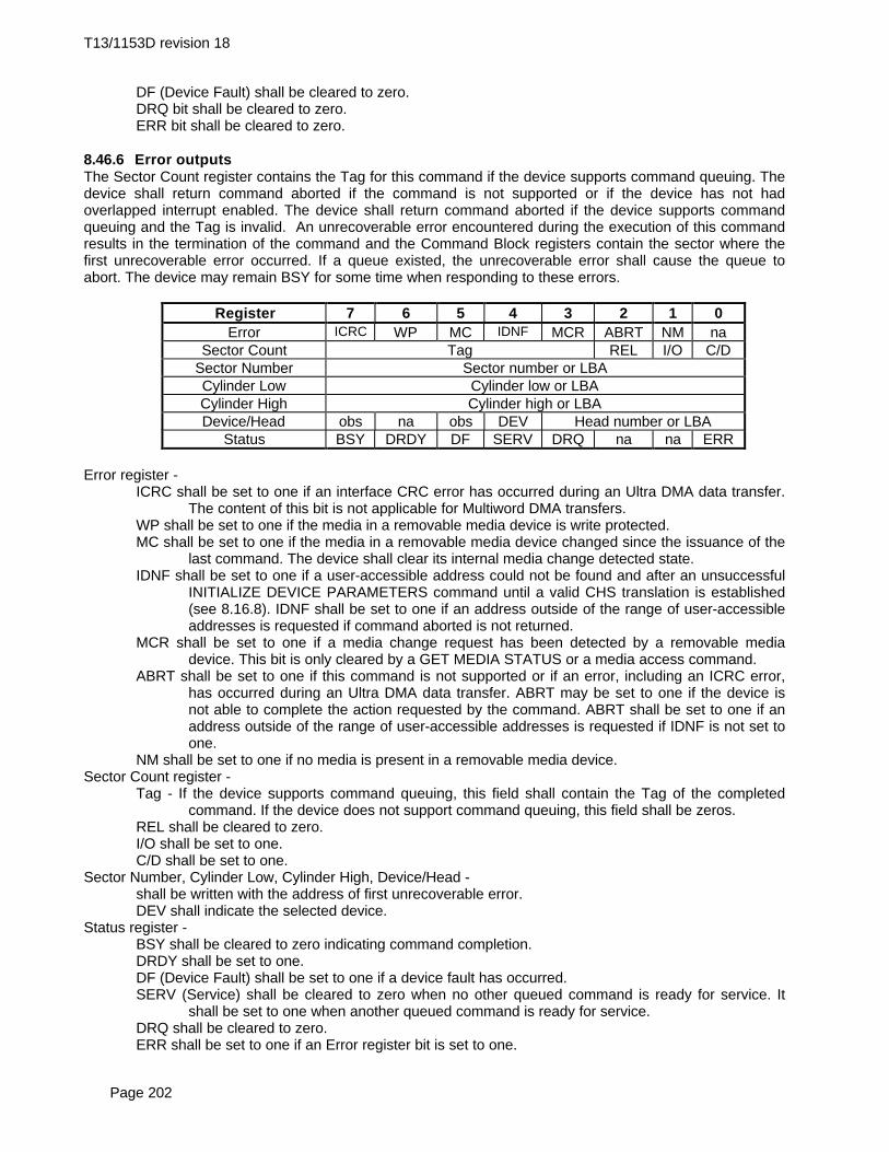
T13/1153D revision 18
Page 202
DF (Device Fault) shall be cleared to zero.DRQ bit shall be cleared to zero.ERR bit shall be cleared to zero.
8.46.6 Error outputsThe Sector Count register contains the Tag for this command if the device supports command queuing. Thedevice shall return command aborted if the command is not supported or if the device has not hadoverlapped interrupt enabled. The device shall return command aborted if the device supports commandqueuing and the Tag is invalid. An unrecoverable error encountered during the execution of this commandresults in the termination of the command and the Command Block registers contain the sector where thefirst unrecoverable error occurred. If a queue existed, the unrecoverable error shall cause the queue toabort. The device may remain BSY for some time when responding to these errors.
Register 7 6 5 4 3 2 1 0Error ICRC WP MC IDNF MCR ABRT NM na
Sector Count Tag REL I/O C/DSector Number Sector number or LBACylinder Low Cylinder low or LBACylinder High Cylinder high or LBADevice/Head obs na obs DEV Head number or LBA
Status BSY DRDY DF SERV DRQ na na ERR
Error register -ICRC shall be set to one if an interface CRC error has occurred during an Ultra DMA data transfer.
The content of this bit is not applicable for Multiword DMA transfers.WP shall be set to one if the media in a removable media device is write protected.MC shall be set to one if the media in a removable media device changed since the issuance of the
last command. The device shall clear its internal media change detected state.IDNF shall be set to one if a user-accessible address could not be found and after an unsuccessful
INITIALIZE DEVICE PARAMETERS command until a valid CHS translation is established(see 8.16.8). IDNF shall be set to one if an address outside of the range of user-accessibleaddresses is requested if command aborted is not returned.
MCR shall be set to one if a media change request has been detected by a removable mediadevice. This bit is only cleared by a GET MEDIA STATUS or a media access command.
ABRT shall be set to one if this command is not supported or if an error, including an ICRC error,has occurred during an Ultra DMA data transfer. ABRT may be set to one if the device isnot able to complete the action requested by the command. ABRT shall be set to one if anaddress outside of the range of user-accessible addresses is requested if IDNF is not set toone.
NM shall be set to one if no media is present in a removable media device.Sector Count register -
Tag - If the device supports command queuing, this field shall contain the Tag of the completedcommand. If the device does not support command queuing, this field shall be zeros.
REL shall be cleared to zero.I/O shall be set to one.C/D shall be set to one.
Sector Number, Cylinder Low, Cylinder High, Device/Head -shall be written with the address of first unrecoverable error.DEV shall indicate the selected device.
Status register -BSY shall be cleared to zero indicating command completion.DRDY shall be set to one.DF (Device Fault) shall be set to one if a device fault has occurred.SERV (Service) shall be cleared to zero when no other queued command is ready for service. It
shall be set to one when another queued command is ready for service.DRQ shall be cleared to zero.ERR shall be set to one if an Error register bit is set to one.
T13/1153D revision 18
Page 203
8.46.7 PrerequisitesDRDY set to one. The host shall initialize the DMA channel.
8.46.8 DescriptionThis command executes in a similar manner to a WRITE DMA command. The device may perform a busrelease the bus or it may execute the data transfer without performing a bus release if the data is ready totransfer.
If the device performs a bus release, the host shall reselect the device using the SERVICE command.
Once the data transfer is begun, the device shall not perform a bus release until the entire data transfer hasbeen completed.
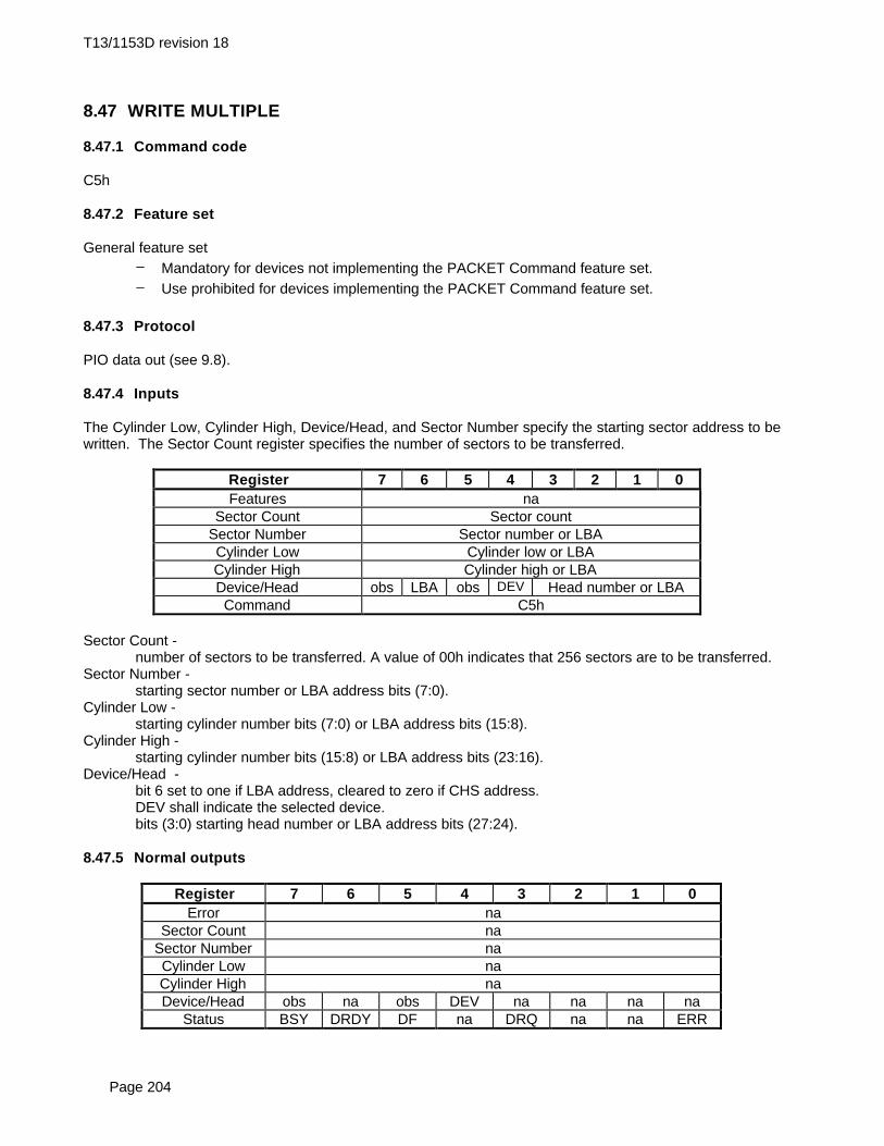
T13/1153D revision 18
Page 204
8.47 WRITE MULTIPLE
8.47.1 Command code
C5h
8.47.2 Feature set
General feature set− Mandatory for devices not implementing the PACKET Command feature set.− Use prohibited for devices implementing the PACKET Command feature set.
8.47.3 Protocol
PIO data out (see 9.8).
8.47.4 Inputs
The Cylinder Low, Cylinder High, Device/Head, and Sector Number specify the starting sector address to bewritten. The Sector Count register specifies the number of sectors to be transferred.
Register 7 6 5 4 3 2 1 0Features na
Sector Count Sector countSector Number Sector number or LBACylinder Low Cylinder low or LBACylinder High Cylinder high or LBADevice/Head obs LBA obs DEV Head number or LBACommand C5h
Sector Count -number of sectors to be transferred. A value of 00h indicates that 256 sectors are to be transferred.
Sector Number -starting sector number or LBA address bits (7:0).
Cylinder Low -starting cylinder number bits (7:0) or LBA address bits (15:8).
Cylinder High -starting cylinder number bits (15:8) or LBA address bits (23:16).
Device/Head -bit 6 set to one if LBA address, cleared to zero if CHS address.DEV shall indicate the selected device.bits (3:0) starting head number or LBA address bits (27:24).
8.47.5 Normal outputs
Register 7 6 5 4 3 2 1 0Error na
Sector Count naSector Number naCylinder Low naCylinder High naDevice/Head obs na obs DEV na na na na
Status BSY DRDY DF na DRQ na na ERR

T13/1153D revision 18
Page 205
Device/Head register -DEV shall indicate the selected device.
Status register -BSY shall be cleared to zero indicating command completion.DRDY shall be set to one.DF (Device Fault) shall be cleared to zero.DRQ shall be cleared to zero.ERR shall be cleared to zero.
8.47.6 Error outputs
An unrecoverable error encountered during the execution of this command results in the termination of thecommand. The Command Block registers contain the address of the sector where the first unrecoverableerror occurred. The amount of data transferred is indeterminate.
Register 7 6 5 4 3 2 1 0Error na WP MC IDNF MCR ABRT NM na
Sector Count naSector Number Sector number or LBACylinder Low Cylinder low or LBACylinder High Cylinder high or LBADevice/Head obs na obs DEV Head number or LBA
Status BSY DRDY DF na DRQ na na ERR
Error register -WP shall be set to one if the media in a removable media device is write protected.MC shall be set to one if the media in a removable media device changed since the issuance of the
last command. The device shall clear its internal media change detected state.IDNF shall be set to one if a user-accessible address could not be found and after an unsuccessful
INITIALIZE DEVICE PARAMETERS command until a valid CHS translation is established(see 8.16.8). IDNF shall be set to one if an address outside of the range of user-accessibleaddresses is requested if command aborted is not returned.
MCR shall be set to one if a media change request has been detected by a removable mediadevice. This bit is only cleared by a GET MEDIA STATUS or a media access command.
ABRT shall be set to one if this command is not supported or if an error, including an ICRC error,has occurred during an Ultra DMA data transfer. ABRT may be set to one if the device isnot able to complete action requested by the command. ABRT shall be set to one if anaddress outside of the range of user-accessible addresses is requested if IDNF is not set toone.
NM shall be set to one if no media is present in a removable media device.Sector Number, Cylinder Low, Cylinder High, Device/Head -
shall be written with the address of first unrecoverable error.DEV shall indicate the selected device.
Status register -BSY shall be cleared to zero indicating command completion.DRDY shall be set to one.DF (Device Fault) shall be set to one if a device fault has occurred.DRQ shall be cleared to zero.ERR shall be set to one if an Error register bit is set to one.
8.47.7 Prerequisites
DRDY set equal to one. If bit 8 of IDENTIFY DEVICE word 59 is equal to zero, a successful SET MULTIPLEMODE command shall proceed a WRITE MULTIPLE command.

T13/1153D revision 18
Page 206
8.47.8 Description
This command is similar to the WRITE SECTOR(S) command. Interrupts are not generated on everysector, but on the transfer of a block that contains the number of sectors defined by SET MULTIPLE MODEor the default if no intervening SET MULTIPLE command has been issued.
Command execution is identical to the WRITE SECTOR(S) operation except that the number of sectorsdefined by the SET MULTIPLE MODE command are transferred without intervening interrupts. The DRQbit qualification of the transfer is required only at the start of the data block, not on each sector.
The block count of sectors to be transferred without intervening interrupts is the default or programmed bythe SET MULTIPLE MODE command, that shall be executed prior to the WRITE MULTIPLE command.
When the WRITE MULTIPLE command is issued, the Sector Count register contains the number of sectors(not the number of blocks or the block count) requested.
If the number of requested sectors is not evenly divisible by the block count, as many full blocks as possibleare transferred, followed by a final, partial block transfer. The partial block transfer is for n sectors, where:
n = Remainder (sector count/ block count).
If the WRITE MULTIPLE command is received when WRITE MULTIPLE commands are disabled, the WriteMultiple operation shall be rejected with command aborted.
Device errors encountered during WRITE MULTIPLE commands are posted after the attempted devicewrite of the block or partial block transferred. The Write command ends with the sector in error, even if itwas in the middle of a block. Subsequent blocks are not transferred in the event of an error.
The contents of the Command Block Registers following the transfer of a data block that had a sector inerror are undefined. The host should retry the transfer as individual requests to obtain valid errorinformation. Interrupts are generated when the DRQ bit is set to one at the beginning of each block orpartial block.
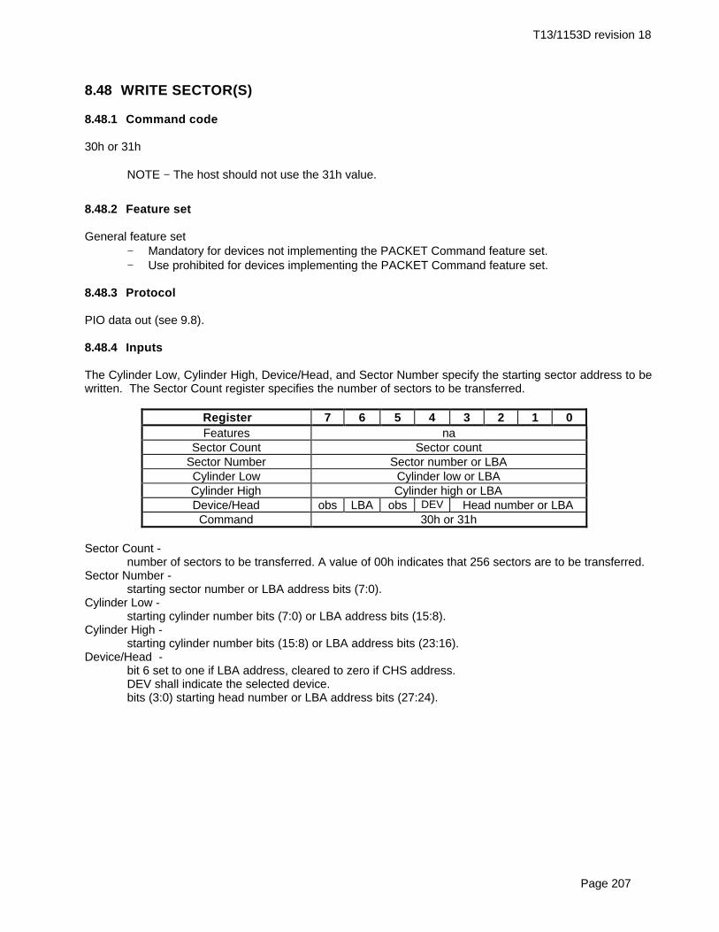
T13/1153D revision 18
Page 207
8.48 WRITE SECTOR(S)
8.48.1 Command code
30h or 31h
NOTE − The host should not use the 31h value.
8.48.2 Feature set
General feature set− Mandatory for devices not implementing the PACKET Command feature set.− Use prohibited for devices implementing the PACKET Command feature set.
8.48.3 Protocol
PIO data out (see 9.8).
8.48.4 Inputs
The Cylinder Low, Cylinder High, Device/Head, and Sector Number specify the starting sector address to bewritten. The Sector Count register specifies the number of sectors to be transferred.
Register 7 6 5 4 3 2 1 0Features na
Sector Count Sector countSector Number Sector number or LBACylinder Low Cylinder low or LBACylinder High Cylinder high or LBADevice/Head obs LBA obs DEV Head number or LBACommand 30h or 31h
Sector Count -number of sectors to be transferred. A value of 00h indicates that 256 sectors are to be transferred.
Sector Number -starting sector number or LBA address bits (7:0).
Cylinder Low -starting cylinder number bits (7:0) or LBA address bits (15:8).
Cylinder High -starting cylinder number bits (15:8) or LBA address bits (23:16).
Device/Head -bit 6 set to one if LBA address, cleared to zero if CHS address.DEV shall indicate the selected device.bits (3:0) starting head number or LBA address bits (27:24).

T13/1153D revision 18
Page 208
8.48.5 Normal outputs
Register 7 6 5 4 3 2 1 0Error na
Sector Count naSector Number naCylinder Low naCylinder High naDevice/Head obs na obs DEV na na na na
Status BSY DRDY DF na DRQ na na ERR
Device/Head register -DEV shall indicate the selected device.
Status register -BSY shall be cleared to zero indicating command completion.DRDY shall be set to one.DF (Device Fault) shall be cleared to zero.DRQ shall be cleared to zero.ERR shall be cleared to zero.
8.48.6 Error outputs
An unrecoverable error encountered during the execution of this command results in the termination of thecommand. The Command Block registers contain the address of the sector where the first unrecoverableerror occurred. The amount of data transferred is indeterminate.
Register 7 6 5 4 3 2 1 0Error na WP MC IDNF MCR ABRT NM na
Sector Count naSector Number Sector number or LBACylinder Low Cylinder low or LBACylinder High Cylinder high or LBADevice/Head obs na obs DEV Head number or LBA
Status BSY DRDY DF na DRQ na na ERR
Error register -WP shall be set to one if the media in a removable media device is write protected.MC shall be set to one if the media in a removable media device changed since the issuance of the
last command. The device shall clear its internal media change detected state.IDNF shall be set to one if a user-accessible address could not be found and after an unsuccessful
INITIALIZE DEVICE PARAMETERS command until a valid CHS translation is established(see 8.16.8). IDNF shall be set to one if an address outside of the range of user-accessibleaddresses is requested if command aborted is not returned.
MCR shall be set to one if a media change request has been detected by a removable mediadevice. This bit is only cleared by a GET MEDIA STATUS or a media access command.
ABRT shall be set to one if this command is not supported or if an error, including an ICRC error,has occurred during an Ultra DMA data transfer. ABRT may be set to one if the device isnot able to complete the action requested by the command. ABRT shall be set to one if anaddress outside of the range of user-accessible addresses is requested if IDNF is not set toone.
NM shall be set to one if no media is present in a removable media device.Sector Number, Cylinder Low, Cylinder High, Device/Head -
shall be written with the address of first unrecoverable error.DEV shall indicate the selected device.
Status register -BSY shall be cleared to zero indicating command completion.DRDY shall be set to one.

T13/1153D revision 18
Page 209
DF (Device Fault) shall be set to one if a device fault has occurred.DRQ shall be cleared to zero.ERR shall be set to one if an Error register bit is set to one.
8.48.7 Prerequisites
DRDY set equal to one.
8.48.8 Description
This command writes from 1 to 256 sectors as specified in the Sector Count register. A sector count of 0requests 256 sectors.

T13/1153D revision 18
Page 210
9 Protocol
Commands are grouped into different classes according to the protocols followed for command execution.The command classes with their associated protocols are defined below.
For all commands except DEVICE RESET, the host first checks if the BSY bit is equal to one, and shouldproceed no further unless and until the BSY bit is equal to zero. For most commands, the host shall alsowait for the DRDY bit to be equal to one before proceeding.
Data transfers may be accomplished in more ways than are described below, but these sequences shouldwork with all known implementations of devices.
A device shall maintain either the BSY bit equal to one or the DRQ bit equal to one at all times untilcommand completion. The INTRQ signal is used by the device to signal most, but not all, times when theBSY bit is changed from one to zero during command execution and command completion.
The result of writing to the Command register or a hardware or software reset while the BSY bit is equal toone or the DRQ bit is equal to one may result in data corruption for commands that were queued or inprogress at the time.
9.1 Signature and persistence
A device not implementing the PACKET command feature set shall place the signature in the CommandBlock registers listed below for power on reset, hardware reset, software reset, and the EXECUTE DEVICEDIAGNOSTIC command.
If the device does not implement the PACKET command feature set, the signature shall be:Sector Count 01h
Sector Number 01hCylinder Low 00hCylinder High 00hDevice/Head 00h
A device implementing the PACKET command feature set shall place the signature in the Command Blockregisters listed below for power on reset, hardware reset, software reset, the EXECUTE DEVICEDIAGNOSTIC command, and the DEVICE RESET command. The DEVICE RESET command shall notchange the value of the DEV bit when writing the signature into the Device/Head register for a deviceimplementing the PACKET command feature set. If the device implements the PACKET command featureset, the signature is also written in the registers for the IDENTIFY DEVICE and READ SECTOR(S)commands.
If the device implements the PACKET command feature set, the signature shall be:Sector Count 01h
Sector Number 01hCylinder Low 14hCylinder High EBhDevice/Head 00h or 10h
If the PACKET command feature set is implemented by a device, then the signature values written by thedevice in the Command Block registers following power on reset, hardware reset, software reset, or theDEVICE RESET command shall not be changed by the device until the device receives a command thatsets DRDY to one. These commands are a PACKET command or an IDENTIFY PACKET DEVICEcommand. Writes by the host to the Command Block registers that contain the signature values shalloverwrite the signature values and invalidate the signature.

T13/1153D revision 18
Page 211
9.2 Power on and hardware resets
This clause describes the algorithm and timing relationships for Device 0 and Device 1 during theprocessing of power on and hardware resets.
If the host asserts RESET- while a device is in or going to a power management mode, then the device shallexecute its hardware reset sequence.
If the host reasserts RESET- before devices have completed executing their power on or hardware resetsequences, then the devices shall restart executing their hardware reset sequence at step (b).
The host should not set the SRST bit to one in the Device Control register or issue a DEVICE RESETcommand while the BSY bit is set to one in either devices’ Status register as a result of executing a poweron or hardware reset sequence. If the host sets the SRST bit in the Device Control register to one or issuesa DEVICE RESET command before the devices have completed execution of their power on or hardwarereset sequences, then the devices shall ignore the software reset or DEVICE RESET command.
A host should issue an IDENTIFY DEVICE and/or IDENTIFY PACKET DEVICE command after a issuing asoftware reset in order to correctly determine the current status of features implemented by the device(s).
If the device has not determined its device number, the device shall follow the protocol described in steps(a) through (c) of 9.2.1 until the device number is determined.
The host shall not begin polling the Status register until at least 2 ms after RESET- is negated. The hostshould only interpret bits 6 and 7 of the Status register to determine completion of the reset.
9.2.1 Power on and hardware resets - device 0
The following steps should occur sequentially as listed. Several of the steps may occur concurrently oroutside of the listed sequence when explicitly allowed so long as all timing relationships are satisfied, e.g.:Device 0 may continue to sample DASP- after Device 0 has completed its hardware initialization and self-diagnostic testing.
Steps (b) through (o) shall be completed within 31s from negation of RESET- by the host.
a) The host shall assert RESET- for a minimum of 25 µs after power to the device has stabilized within thesystem’s specified tolerance. The device shall not recognize a signal assertion shorter than 20 ns as avalid RESET signal. Devices may respond to any signal assertion greater than 20 ns and shallrecognize a signal equal to or greater than 25 us;
b) The device shall release PDIAG-, INTRQ, IORDY, DMARQ, and DD(15:0) no later than 400 ns afterRESET- is negated;
c) The device shall set the BSY bit to one no later than 400 ns after RESET- is negated;d) The device shall determine that it is Device 0;e) The device shall release DASP- no later than 1 ms after RESET- is negated;f) Steps (b), (c), (d), and (e) shall be completed before continuing;g) Device 0 shall sample DASP- for assertion by Device 1. Device 0 may sample DASP- at any
frequency. This sampling shall not begin until at least 1 ms after RESET- is negated. Device 0 maystop sampling DASP- upon detection of its assertion. The last sample of DASP- by Device 0 shall occurno sooner than 450 ms after RESET- is negated if assertion has not been detected before this time.Device 0 shall not sample DASP- later than 5 s after RESET- is negated;
h) Step (g) shall be completed before executing the following: Device 0 shall store whether or not Device1 was detected in step (g). This information is needed to process any future software reset orEXECUTE DEVICE DIAGNOSTIC command. This information shall be saved by Device 0 until thenext power on or hardware reset;
i) Device 0 should begin performing its hardware initialization and self-diagnostic testing;j) Device 0 may revert to its default condition (the device’s settings may now be in different conditions
than they were before RESET- was asserted by the host). All Ultra DMA modes shall be disabled;
T13/1153D revision 18
Page 212
k) Step (g) shall be completed before executing the following: if Device 0 did not detect that DASP- wasasserted by Device 1 during step (g) (i.e.: Device 1 is not present), then Device 0 shall clear bit 7 tozero in the Error register and go to step (m);
l) Device 0 shall sample PDIAG- for assertion by Device 1. Device 0 may sample PDIAG- at anyfrequency. This sampling shall not begin until at least 1 ms after RESET- is negated. Device 0 maystop sampling PDIAG- upon detection of its assertion. The last sample of PDIAG- by Device 0 shalloccur no sooner than 450 ms after RESET- is negated if assertion has not been detected before thistime. Device 0 shall not sample PDIAG- later than 31 s after RESET- is negated;1) If Device 0 detects that PDIAG- is asserted within 31 s after RESET- is negated, then Device 0 shall
clear bit 7 to zero in the Error register;2) If Device 0 does not detect that PDIAG- is asserted within 31 s after RESET- is negated, then
Device 0 shall set bit 7 to one in the Error register;m) If performed, the hardware initialization and self-diagnostic testing initiated in step (i) shall be completed
before executing the following: Device 0 shall write its self-diagnostic testing results to bits 6-0 in theError register. Table 10 defines results values;
n) Device 0 shall set its signature values (see 9.1) and clear SRST in the Device Control register to zero.The effect on the Features register is undefined;
o) Clearing Status register bits:1) If the PACKET command feature set is not implemented by Device 0, Device 0 shall clear to zero
bits 3, 2, and 0 of the Status register;2) If the PACKET command feature set is implemented by Device 0, Device 0 shall clear to zero bits
5, 4, 3, 2, and 0 of the Status register;p) Clearing BSY:
1) If the PACKET command feature set is not implemented by Device 0, then steps (h), (j), (k), (l) (asrequired), (m), and (n) shall be completed before executing the following: Device 0 shall clear theBSY bit to zero when ready to accept commands that do not require the DRDY bit to be equal to one;
2) If the PACKET command feature set is implemented by Device 0, then Device 0 shall return itsoperating modes to their specified initial conditions: MODE SELECT conditions shall be restored totheir last saved values if saved values have been established; MODE SELECT conditions for whichno values have been saved shall be returned to their default values; then Device 0 shall clear theBSY bit to zero when ready to accept commands;
q) Setting DRDY:1) If the PACKET command feature set is not implemented by Device 0, then the DRDY bit shall be
set to one within 30 s after the BSY bit has been cleared to zero. Steps (p) (1) and (q) (1) mayoccur at the same time;
2) If the PACKET command feature set is implemented by Device 0, then Device 0 shall not set DRDYto one;
9.2.2 Power on and hardware resets - device 1
The following steps should occur sequentially as listed. Several of the steps may occur concurrently oroutside of the listed sequence when explicitly allowed so long as all timing relationships are satisfied.
Steps (b) through (m) shall be completed by Device 1 within 30 s from negation of RESET- by the host.
a) The host shall assert RESET- for a minimum of 25 µs after power to the device has stabilized within thesystem’s specified tolerance. The device shall not recognize a signal assertion shorter than 20 ns as avalid RESET signal. Devices may respond to any signal assertion greater than 20 ns and shallrecognize a signal equal to or greater than 25 us;
b) The device shall release INTRQ, IORDY, DMARQ, and DD(15:0) no later than 400 ns after RESET- isnegated;
c) The device shall set the BSY bit to one no later than 400 ns after RESET- is negated;d) The device shall determine that it is Device 1;e) Device 1 shall negate PDIAG- no later than 1 ms after RESET- is negated;f) Steps (b), (c), (d), and (e) shall be completed before continuing;g) Device 1 shall assert DASP- no later than 400 ms after RESET- is negated:h) Device 1 should begin performing its hardware initialization and self-diagnostic testing;

T13/1153D revision 18
Page 213
i) Device 1 may revert to its default condition (the device’s settings may now be in different conditionsthan they were before the RESET- was asserted by the host). All Ultra DMA modes shall be disabled;
j) If performed, the hardware initialization and self-diagnostic testing initiated in step (h) shall becompleted before executing the following: Device 1 shall write its self-diagnostic testing results to theError register. Table 10 defines the results values;
k) Device 1 shall set its signature values (see 9.1) and clear SRST in the Device Control register to zero.The effect on the Features register is undefined;
l) Clearing Status register bits:1) If the PACKET command feature set is not implemented by Device 1, Device 1 shall clear to zero
bits 3, 2, and 0 of the Status register;2) If the PACKET command feature set is implemented by Device 1, Device 1 shall clear to zero bits
5, 4, 3, 2, and 0 of the Status register;m) Clearing BSY:
1) If the PACKET command feature set is not implemented by Device 1, then steps (g), (i), (j), and (k)shall be completed before executing the following: Device 1 shall clear the BSY bit to zero whenready to accept commands that do not require the DRDY bit to be equal to one;
2) If the PACKET command feature set is implemented by Device 1, then Device 1 shall return itsoperating modes to their specified initial conditions: MODE SELECT conditions shall be restored totheir last saved values if saved values have been established; MODE SELECT conditions for whichno values have been saved shall be returned to their default values; then Device 1 shall clear theBSY bit to zero when ready to accept commands;
n) Step (l) shall be completed before executing the following: If Device 1 passed its self-diagnostic testing,then Device 1 shall assert PDIAG-;
o) Setting DRDY:1) If the PACKET command feature set is not implemented by Device 1, then the DRDY bit shall be
set to one within 30 s after the BSY bit has been cleared to zero. Steps (m) (1), (n), and (o) (1) mayoccur at the same time;
2) If the PACKET command feature set is implemented by Device 1, then Device 1 shall not set DRDYto one;
p) Device 1 shall continue to assert DASP- and PDIAG- until after the first command is received from thehost or until at least 31 s after RESET- is negated or until detecting that the host has set the SRST bit toone in the Device Control register, whichever comes first. Device 1 shall release PDIAG- no later thancommand completion of the next command from the host except for the EXECUTE DEVICEDIAGNOSTIC command.

T13/1153D revision 18
Page 214
t10RESET-
t11Device 0 BSY
Device 0 DRDY
Device 0 PDIAG- out
Device 0 DASP- outt12
t13
Device 0 DASP- in
Device 0 PDIAG- in
t14t15
Device 1 BSY
Device 1 DRDY
t16
Device 1 DASP- outt17
t18Device 1 PDIAG- out
Figure 8 −− BSY and DRDY timing for power on and hardware resets

T13/1153D revision 18
Page 215
Table 25 −− BSY and DRDY timing for power on and hardware resetsRESET- timing parameters Min Max Note
t10 RESET- pulsewidth 25 µs 1t11 Device 0 RESET- negation to BSY bit set to
one, release PDIAG-400 ns
t12 Device 0 release DASP- 1 mst13 Device 0 sample of DASP- 1 ms 450 ms 2t14 Device 0 sample of PDIAG- 1 ms 31 s 3t15 Device 1 RESET- negation to BSY bit set to
onet16 Device 1 assert DASP- 400 mst17 Device 1 negate PDIAG- if asserted 1 mst18 Device 1 assert PDIAG- 30 s 4
NOTES −1 The device shall not recognize a RESET- assertion pulse width shorter than 20 ns as avalid signal assertion.2 Device 0 shall sample beginning 1 ms after RESET- is negated. Sampling shallcontinue until DASP- assertion by Device 1 is sensed or 450 ms has elapsed indicatingno Device 1 present.3 Device 0 shall sample beginning 1 ms after RESET- is negated. Sampling shallcontinue until:
a) no DASP- assertion is sensed in 450 ms;b) DASP- assertion is sensed in 450 ms and PDIAG- assertion is sensed;c) or DASP- assertion is sensed in 450 ms and no PDIAG- assertion is sensed
in 31s.When sampling is stopped, Device 0 shall clear the BSY bit to zero. DRDY shall be set toone when Device 0 is ready to accept any command. No maximum time is specified buta host should allow up to 30 s from the time RESET- is negated.4 Upon completion of internal diagnostics, Device 1 shall clear BSY to zero, and ifdiagnostics passed, assert PDIAG-. Internal diagnostics shall complete within 30 s of thenegation of RESET-.
9.3 Software reset
This clause describes the algorithm and timing relationships for Device 0 and Device 1 during theprocessing of software resets.
If the host sets the SRST bit in the Device Control register to one while a device is in or going to a powermanagement mode, then the device shall execute its software reset sequence.
If the host asserts RESET- before devices have completed executing their software reset sequences, thenthe devices shall start executing their hardware reset sequence at step (b).
The host should not set the SRST bit to one in the Device Control register while the BSY bit is set to one ineither devices’ Status register as a result of executing a software reset sequence. If the host sets the SRSTbit in the Device Control register to one before the devices have completed execution of their software resetsequences, then the devices shall restart executing their software reset sequences at step (b).
A host should issue an IDENTIFY DEVICE and/or IDENTIFY PACKET DEVICE command after a issuing asoftware reset in order to correctly determine the current status of features implemented by the device(s).
Some devices may take up to 2 ms to set BSY when coming out of Sleep mode. The host shall not beginpolling the Status register until at least 2 ms after the SRST bit has been set to one. The host should onlyinterpret bits 6 and 7 of the Status register to determine completion of the reset.

T13/1153D revision 18
Page 216
9.3.1 Software reset - device 0
The following steps should occur sequentially as listed. Several of the steps may occur concurrently oroutside of the listed sequence when explicitly allowed so long as all timing relationships are satisfied, e.g.,Device 0 may continue to sample PDIAG- after Device 0 has completed writing the specified values to theSector Count, Sector Number, Cylinder Low, Cylinder High, and Device/Head registers.
Steps (g) through (k) shall be completed within 31 s from Device 0 detecting that the SRST bit is cleared tozero.
a) The host shall set the SRST bit to one in the Device Control register. The host shall not clear the SRSTbit to zero until at least 5 µs after setting the bit to one. The host shall not set the SRST bit to one untilthe bit has been cleared to zero for at least 5 µs;
b) The device shall release PDIAG-, INTRQ, IORDY, DMARQ, and DD(15:0) no later than 400 ns afterdetecting that the SRST bit is equal to one;
c) Device 0 shall set the BSY bit to one no later than 400 ns after detecting that the SRST bit is equal toone;
d) Hardware initialization and self-diagnostic testing:1) If the PACKET command feature set is not implemented by the device, the device shall begin
performing its hardware and self-diagnostic testing;2) If the PACKET command feature set is implemented by the device, the device may begin
performing its hardware and self-diagnostic testing and the device is not expected to stop anybackground device activity (e.g., immediate command (see MMC and MMC2)) that was startedprior to the time that the SRST was set to one in step (a);
e) Reverting to default:1) If the PACKET command feature set is not implemented by Device 0, then Device 0 may revert to
its default condition (the device’s settings may now be in different conditions than they were beforethe SRST bit was set to one by the host). However, the condition of any Ultra DMA mode (eitherenabled or disabled) shall not be affected by the host setting the SRST bit to one ;
2) If the PACKET command feature set is implemented by Device 0, then Device 0 shall not revert toits default condition. However, the condition of any Ultra DMA mode (either enabled or disabled)shall not be affected by the host setting the SRST bit to one;
f) Device 0 shall wait for the host to clear the SRST bit to zero before continuing;g) If Device 0 did not detect that DASP- was asserted by Device 1 during the most recent power cycle or
hardware reset, then Device 0 shall clear bit 7 in the Error register to zero and go to step (i);h) If Device 0 detected that DASP- was asserted by Device 1 during the most recent power cycle or
hardware reset, then Device 0 shall sample PDIAG- for assertion by Device 1. Device 0 may samplePDIAG- at any frequency. This sampling shall not begin until at least 1 ms after SRST is cleared tozero. Device 0 may stop sampling PDIAG- upon detection of assertion. Device 0 shall not samplePDIAG- after the first command is received or later than 31 s after SRST is cleared to zero;1) If Device 0 detects that PDIAG- is asserted within 31 s after SRST is cleared to zero, then Device 0
shall clear bit 7 to zero in the Error register;2) If Device 0 does not detect that PDIAG- is asserted within 31 s after SRST is cleared to zero, then
Device 0 shall set bit 7 to one in the Error register;i) If performed, the hardware initialization and self-diagnostic testing initiated in step (d) shall be
completed before executing the following: Device 0 shall write its self-diagnostic testing results to bits6-0 in the Error register. Table 10 defines the results values;
j) Device 0 shall set its signature values (see 9.1). The effect on the Features register is undefined;k) Clearing Status register bits:
1) If the PACKET command feature set is not implemented by Device 0, Device 0 shall clear to zerobits 3, 2, and 0 of the Status register;
2) If the PACKET command feature set is implemented by Device 0, Device 0 shall clear to zero bits5, 3, 2, and 0 of the Status register;

T13/1153D revision 18
Page 217
l) Clearing BSY:1) If the PACKET command feature set is not implemented by Device 0, then Steps (g), (h) (as
required), (i) and (j) shall be completed before executing the following: Device 0 shall clear theBSY bit to zero when ready to accept commands that do not require the DRDY bit to be equal toone.
2) If the PACKET command feature set is implemented by Device 0, then Device 0 shall return itsoperating modes to their specified initial conditions: MODE SELECT conditions shall be restored totheir last saved values if saved values have been established; MODE SELECT conditions for whichno values have been saved shall be returned to their default values; then Device 0 shall clear theBSY bit to zero when ready to accept commands;
m) Setting DRDY:1) If the PACKET command feature set is not implemented by Device 0, then the DRDY bit shall be
set to one within 30 s after the BSY bit has been cleared to zero. Steps (l) (1) and (m) (1) mayoccur at the same time;
2) If the PACKET command feature set is implemented by Device 0, then Device 0 shall not setDRDY to one;
9.3.2 Software reset - device 1
The following steps should occur sequentially as listed. Several of the steps may occur concurrently oroutside of the listed sequence when explicitly allowed so long as all timing relationships are satisfied.
Steps (h) through (k) shall be completed within 30 s from Device 1 detecting that the SRST bit is cleared tozero.
a) The host shall set the SRST bit to one in the Device Control register. The host shall not clear the SRSTbit to zero until at least 5 µs after setting the bit to one. The host shall not set the SRST bit to one untilthe bit has been cleared to zero for at least 5 µs;
b) The device shall release INTRQ, IORDY, DMARQ, and DD(15:0) no later than 400 ns after detectingthat the SRST bit is equal to one;
c) Device 1 shall set the BSY bit to one no later than 400 ns after detecting that the SRST bit is equal toone;
d) Device 1 shall negate PDIAG- no later than 1 ms after detecting that the SRST bit is equal to one;e) Hardware initialization and self-diagnostic testing:
1) If the PACKET command feature set is not implemented by the device, the device shall beginperforming its hardware and self-diagnostic testing;
2) If the PACKET command feature set is implemented by the device, the device may beginperforming its hardware and self-diagnostic testing and the device is not expected to stop anybackground device activity (e.g., immediate command (see MMC and MMC2)) that was started priorto the time that the SRST was set to one in step (a);
f) Reverting to default:1) If the PACKET command feature set is not implemented by Device 1, then Device 1 may revert to
its default condition (the device’s settings may now be in different conditions than they were beforethe SRST bit was set to one by the host). However, the condition of any Ultra DMA mode (eitherenabled or disabled) shall not be affected by the host setting the SRST bit to one;
2) If the PACKET command feature set is implemented by Device 1, then Device 1 shall not revert toits default condition. However, the condition of any Ultra DMA mode (either enabled or disabled)shall not be affected by the host setting the SRST bit to one;
g) Device 1 shall wait for the host to clear the SRST bit to zero before continuing;h) If performed, the hardware initialization and self-diagnostic testing initiated in step (e) shall be
completed before executing the following: Device 1 shall write its self-diagnostic testing results to theError register. Table 10 defines the results values;
i) Device 1 shall set its signature values (see 9.1). The effect on the Features register is undefined;j) Clearing Status register bits:
1) If the PACKET command feature set is not implemented by Device 1, Device 1 shall clear to zerobits 3, 2, and 0 of the Status register;
2) If the PACKET command feature set is implemented by Device 1, Device 1 shall clear to zero bits5, 3, 2, and 0 of the Status register;

T13/1153D revision 18
Page 218
k) Clearing BSY:1) If the PACKET command feature set is not implemented by Device 1, then steps (h) and (i) shall be
completed before executing the following: Device 1 shall clear the BSY bit to zero when ready toaccept commands that do not require the DRDY bit to be equal to one;
2) If the PACKET command feature set is implemented by Device 1, then Device 1 shall return itsoperating modes to their specified initial conditions: MODE SELECT conditions shall be restored totheir last saved values if saved values have been established; MODE SELECT conditions for whichno values have been saved shall be returned to their default values; then Device 1 shall clear theBSY bit to zero when ready to accept commands;
l) Step (j) shall be completed before executing the following: If Device 1 passed its self-diagnostic testing,then Device 1 shall assert PDIAG-;
m) Setting DRDY:1) If the PACKET command feature set is not implemented by Device 1, then the DRDY bit shall be
set to one within 30 s after the BSY bit has been cleared to zero. Steps (k) (1), (l), and (m) (1) mayoccur at the same time;
2) If the PACKET command feature set is implemented by Device 1, then Device 1 shall not set DRDYto one;
n) Device 1 shall continue to assert PDIAG- until after the first command is received from the host or untilat least 31 s after detecting that SRST is cleared to zero or until detecting that the host has set theSRST bit to one in the Device Control register, whichever comes first. Device 1 shall release PDIAG- nolater than command completion of the next command from the host except for the EXECUTE DEVICEDIAGNOSTIC command.
t20
SRST
t21
Device 0 BSY
Device 0 DRDY
Device 0 PDIAG- out
Device 0 PDIAG- in
t22t23
Device 1 BSY
Device 1 DRDYt24
t25
Device 1 PDIAG- out
Figure 9 −− BSY and DRDY timing for software reset

T13/1153D revision 18
Page 219
Table 26 −− BSY and DRDY timing for software resetSRST timing parameters Min Max Note
t20 SRST bit set to one 5 µst21 Device 0 SRST set to one to BSY bit set to one,
release PDIAG-400 ns
t22 Device 0 SRST cleared to zero to sample of PDIAG- 1 ms 31 s 1t23 Device 1 SRST set to one to BSY set to one 400 nst24 Device 1 SRST cleared to zero to BSY bit cleared to
zero, PDIAG- asserted30 s 2
t25 Device 1 negate PDIAG- if asserted 1 msNOTES −1 Device 0 shall sample beginning 1 ms after SRST is cleared to zero. Sampling shall continueuntil PDIAG- assertion by Device 1 is sensed or 31 s has elapsed indicating Device 1 faileddiagnostic.2 Upon completion of internal diagnostics, Device 1 shall clear BSY to zero, and if diagnosticspassed, assert PDIAG-. Internal diagnostics shall complete within 30 s of the SRST beingcleared to zero.
9.4 DEVICE RESET protocol
If the host asserts RESET- before the device has completed executing a DEVICE RESET command, thenthe device shall start executing its hardware reset sequence at step (b).
If the host sets the SRST bit to one before the device has completed executing a DEVICE RESETcommand, the device shall start executing its software reset sequence at step (b).
The host should not issue a DEVICE RESET command while a DEVICE RESET command is in progress. Ifthe host issues a DEVICE RESET command while a DEVICE RESET command is in progress, the resultsare indeterminate.
The following steps shall occur sequentially as listed.
Steps (b) through (i) shall be completed within 6 s from the device detecting that the command has beenwritten.
a) The host shall write the DEVICE RESET command in the Command register;b) The selected device shall release INTRQ, IORDY, DMARQ, and DD(15:0) no later than 400 ns after
detecting that the command has been written;c) The device shall set the BSY bit to one no later than 400 ns after detecting that the command has been
written;d) The device should stop execution of any uncompleted command. The device is expected to end
background device activity (e.g., immediate commands (see MMC and MMC2));e) The device should not revert to its default condition. If the device reverts to its default condition, the
device shall report a Unit Attention condition to a subsequent PACKET command;f) The device shall clear bit 7 in the Error register to zero;g) The device shall set its signature values (see 9.1). The effect on the Features register is undefined;h) The device shall clear to zero bits 5, 3, 2, and 0 of the Status register;i) MODE SELECT conditions shall not be altered;j) The device shall clear the BSY bit to zero when ready to accept commands that do not require the
DRDY bit to be equal to one;k) The device shall not set DRDY to one.
9.5 EXECUTE DEVICE DIAGNOSTIC protocol
The following steps should occur sequentially as listed. Several of the steps may occur concurrently oroutside of the listed sequence so long as all timing relationships are satisfied, e.g.: Device 0 may continue

T13/1153D revision 18
Page 220
to sample PDIAG- after Device 0 has completed writing the specified values to the Sector Count, SectorNumber, Cylinder Low, Cylinder High, and Device/Head registers.
If the host asserts RESET- before devices have completed executing their EXECUTE DEVICEDIAGNOSTIC sequences, then the devices shall start executing their hardware reset sequence at step (b).
If the host sets the SRST bit in the Device Control register to one before the devices have completedexecution of their EXECUTE DEVICE DIAGNOSTIC sequences, then the devices shall start executing theirsoftware reset sequences at step (b).
The host shall not begin polling the Status register until at least 2 ms after the EXECUTE DEVICEDIAGNOSTIC command has been issued. The host should only interpret bits 6 and 7 of the Status registerto determine command completion.
9.5.1 EXECUTE DEVICE DIAGNOSTIC - Device 0
Device 0 performs the following operations for this command.
Steps (a) through (i) shall be completed within 6 s after the EXECUTE DEVICE DIAGNOSTIC command isreceived:
a) The device shall release PDIAG-, INTRQ, IORDY, DMARQ, and DD(15:0) no later than 400 ns after theEXECUTE DEVICE DIAGNOSTIC command is received;
b) Device 0 shall set the BSY bit to one no later than 400 ns after the EXECUTE DEVICE DIAGNOSTICcommand is received;
c) Device 0 should begin performing its self-diagnostic testing;d) Steps (a), (b), and (c) shall be completed before continuing;e) If Device 0 did not detect that DASP- was asserted by Device 1 during the most recent power cycle or
hardware reset, then Device 0 shall clear bit 7 to zero in the Error register and go to step (g);f) If Device 0 detected that DASP- was asserted by Device 1 during the most recent power cycle or
hardware reset, then Device 0 shall sample PDIAG- for assertion by Device 1. Device 0 may samplePDIAG- at any frequency. This sampling shall not begin until at least 1 ms after the EXECUTE DEVICEDIAGNOSTIC command is received. Device 0 may stop sampling PDIAG- upon detection of assertion.Device 0 shall not sample PDIAG- later than 6 s after the EXECUTE DEVICE DIAGNOSTIC commandis received after the next command is received;1) If Device 0 detects that PDIAG- is asserted within 6 s after the EXECUTE DEVICE DIAGNOSTIC
command is received, then Device 0 shall clear bit 7 to zero in the Error register;2) If Device 0 does not detect that PDIAG- is asserted within 6 s after the EXECUTE DEVICE
DIAGNOSTIC command is received, then Device 0 shall set bit 7 to one in the Error register;g) If performed, the self-diagnostic testing initiated in step (c) shall be completed before executing the
following: Device 0 shall write its self-diagnostic testing results to bits 6-0 of the Error Register. Table10 defines the results values;
h) Device 0 shall set its signature values (see 9.1). The effect on the Features register is undefined;i) Clearing Status register bits:
1) If the PACKET command feature set is not implemented by Device 0, Device 0 shall clear to zerobits 3, 2, and 0 of the Status register;
2) If the PACKET command feature set is implemented by Device 0, Device 0 shall clear to zero bits5, 4, 3, 2, and 0 of the Status register;
j) Clearing BSY:1) If the PACKET Command feature set is not implemented by Device 0, then Steps (e), (f) (as
required), (g) and (h) shall be completed before executing the following: Device 0 shall clear theBSY bit to zero when ready to accept commands that do not require the DRDY bit to be equal toone.
2) If the PACKET Command feature set is implemented by Device 0, then Device 0 shall return itsoperating modes to their specified initial conditions: MODE SELECT conditions shall be restored totheir last saved values if saved values have been established; MODE SELECT conditions for whichno values have been saved shall be returned to their default values; then Device 0 shall clear theBSY bit to zero when ready to accept commands;

T13/1153D revision 18
Page 221
k) Setting DRDY:1) If the PACKET Command feature set is not implemented by Device 0, then the DRDY bit shall be
set to one within 30 s after the BSY bit has been cleared to zero. Steps (i) (1) and (j) (1) may occurat the same time;
2) If the PACKET Command feature set is implemented by Device 0, then Device 0 shall not setDRDY to one;
l) After completing the above steps, Device 0 shall assert INTRQ if nIEN is cleared to zero.
9.5.2 EXECUTE DEVICE DIAGNOSTIC - Device 1
Device 1 performs the following operations for this command.
The following steps should occur sequentially as listed. Several of the steps may occur concurrently oroutside of the listed sequence so long as all timing relationships are satisfied.
Steps (a) through (i) shall be completed within 5 s after the EXECUTE DEVICE DIAGNOSTIC command isreceived:
a) The device shall release INTRQ, IORDY, DMARQ, and DD(15:0) no later than 400 ns after theEXECUTE DEVICE DIAGNOSTIC command is received;
b) Device 1 shall set the BSY bit to one no later than 400 ns after the EXECUTE DEVICE DIAGNOSTICcommand is received;
c) Device 1 shall negate PDIAG- no later than 1 ms after the EXECUTE DEVICE DIAGNOSTIC commandis received;
d) Device 1 should initiate performance of its self-diagnostic testing;e) Steps (a), (b), (c), and (d) shall be completed before continuing.f) If performed, the self-diagnostic testing initiated in step (d) shall be completed before executing the
following: Device 1 shall write its self-diagnostic testing results to the Error register. Table 10 definesthe results values;
g) Device 1 shall set its signature values (see 9.1). The effect on the Features register is undefined;h) Clearing Status register bits:
1) If the PACKET command feature set is not implemented by Device 1, Device 1 shall clear to zerobits 3, 2, and 0 of the Status register;
2) If the PACKET command feature set is implemented by Device 1, Device 1 shall clear to zero bits5, 4, 3, 2, and 0 of the Status register;
i) Clearing BSY:1) If the PACKET Command feature set is not implemented by Device 1, then steps (f) and (g) shall
be completed, , before executing the following: Device 1 shall clear the BSY bit to zero when readyto accept commands that do not require the DRDY bit to be equal to one;
2) If the PACKET Command feature set is implemented by Device 1, then Device 1 shall return itsoperating modes to their specified initial conditions: MODE SELECT conditions shall be restored totheir last saved values if saved values have been established; MODE SELECT conditions for whichno values have been saved shall be returned to their default values; then Device 1 shall clear theBSY bit to zero when ready to accept commands;
j) Step (h) shall be completed before executing the following: If Device 1 passed its self-diagnostic testingduring step (d), then Device 1 shall assert PDIAG-;
k) Setting DRDY:1) If the PACKET Command feature set is not implemented by Device 1, then the DRDY bit shall be
set to one within 30 s after the BSY bit has been cleared to zero. Steps (h) (1), (i), and (j) (1) mayoccur at the same time;
2) If the PACKET Command feature set is implemented by Device 1, then Device 1 shall not setDRDY to one;
l) Device 1 shall continue to assert PDIAG- until after the first command is received from the host or until31 s after the EXECUTE DEVICE DIAGNOSTIC command is received or until detecting that the hosthas set the SRST bit to one in the Device Control register, whichever comes first. Device 1 shall releasePDIAG- no later than command completion of the next command from the host except for theEXECUTE DEVICE DIAGNOSTIC command.
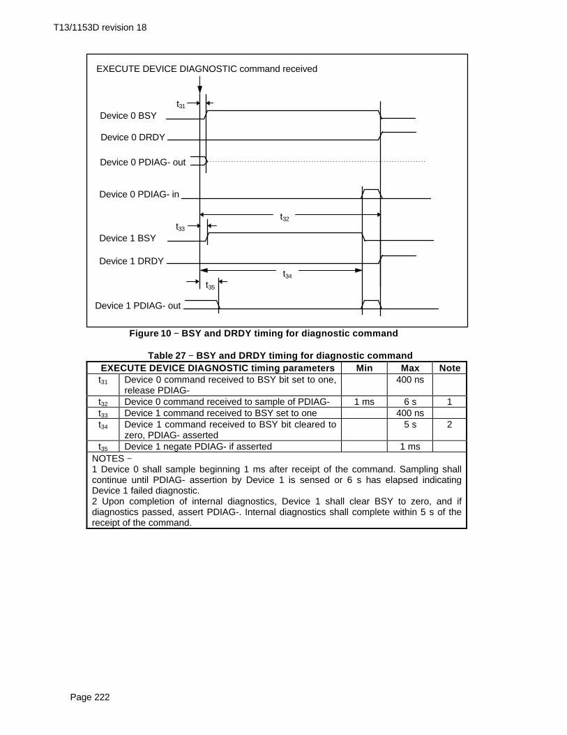
T13/1153D revision 18
Page 222
EXECUTE DEVICE DIAGNOSTIC command received
t31
Device 0 BSY
Device 0 DRDY
Device 0 PDIAG- out
Device 0 PDIAG- in
t32t33
Device 1 BSY
Device 1 DRDYt34
t35
Device 1 PDIAG- out
Figure 10 −− BSY and DRDY timing for diagnostic command
Table 27 −− BSY and DRDY timing for diagnostic commandEXECUTE DEVICE DIAGNOSTIC timing parameters Min Max Notet31 Device 0 command received to BSY bit set to one,
release PDIAG-400 ns
t32 Device 0 command received to sample of PDIAG- 1 ms 6 s 1t33 Device 1 command received to BSY set to one 400 nst34 Device 1 command received to BSY bit cleared to
zero, PDIAG- asserted5 s 2
t35 Device 1 negate PDIAG- if asserted 1 msNOTES −1 Device 0 shall sample beginning 1 ms after receipt of the command. Sampling shallcontinue until PDIAG- assertion by Device 1 is sensed or 6 s has elapsed indicatingDevice 1 failed diagnostic.2 Upon completion of internal diagnostics, Device 1 shall clear BSY to zero, and ifdiagnostics passed, assert PDIAG-. Internal diagnostics shall complete within 5 s of thereceipt of the command.

T13/1153D revision 18
Page 223
9.6 Device selection protocol
Before issuing any command to a device except the DEVICE RESET command, the host shall insure thatthe selected device is no longer busy, select the desired device, and insure that it is ready to accept acommand. Figure 11 describes the protocol for device selection.
Start
Host: Read Status or Alternate Status register
Host: Write the Device/Head register with appropriateDEV bit value (The host shall wait at least 400 ns beforereading the Status register to ensure the content is valid.)
Host: Read Status or Alternate Status register
Host:BSY=0 &DRQ=0?
No
Yes
Host:BSY=0 &DRQ=0 ?
No
Yes
End
Figure 11 −− Device selection protocol

T13/1153D revision 18
Page 224
9.7 PIO data in command protocol
This class includes:
− CFA TRANSLATE SECTOR− IDENTIFY DEVICE− IDENTIFY PACKET DEVICE− READ BUFFER− READ MULTIPLE− READ SECTOR(S)− SMART READ DATA
Execution of this class of command includes the transfer of one or more blocks of data from the device tothe host. Figure 12 describes the protocol of a PIO data in command. This description does not include allpossible error conditions.
Start
Host: Write any required command parameters to theFeatures, Sector Count, Sector Number, CylinderHigh, Cylinder Low, and Device/Head registers
Host: Write command code to the Command register(The host shall wait at least 400 ns before readingthe Status register to ensure the content is valid.)
Device: Set BSY=1 and begin command execution
A
Host: Execute device selectionprotocol described in 9.6
Figure 12 −− PIO data in command protocol (continued)

T13/1153D revision 18
Page 225
B
Device: When ready to transfer data block, set DRQ=1
Device: Clear BSY=0
No
Yes Device:nIEN=0 ?
Device: Assert INTRQ
Host: Read Statusregister
Device: Negate INTRQ
No
Yes Device: Error to report?
A
Device: Set error status
Device:Clear BSY=0
NOTE − Some devicesmay assert DRQ at thistime.
Device: DRQ block transfer complete ?
No
Yes
Host:BSY=0 &DRQ=1?
No
Yes
Host: Read Status register
Host: Read Data register
C
NOTE − Statusregister is read toclear pendinginterupt.
Host: Read Alternate Statusregister and ignore results
NOTE − Thispreventspolling hostfrom readingstatus before itis valid.
Figure 12 −− PIO data in command protocol (continued)
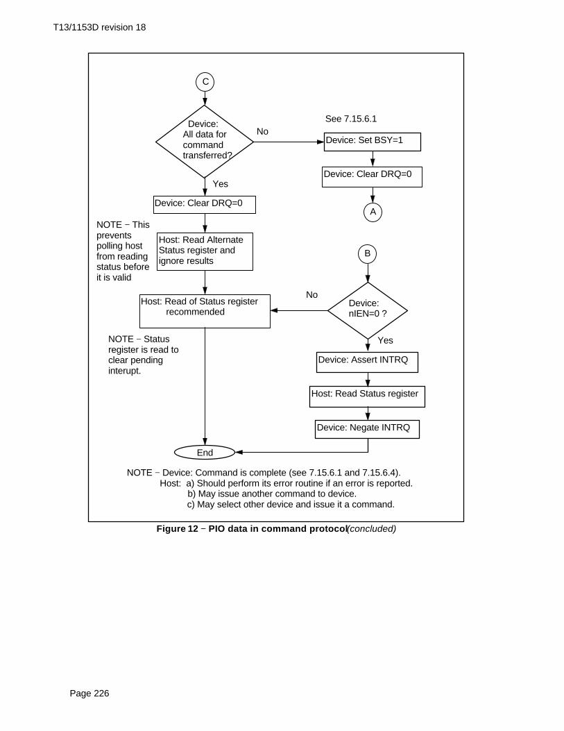
T13/1153D revision 18
Page 226
Host: Read of Status register recommended
NOTE − Device: Command is complete (see 7.15.6.1 and 7.15.6.4). Host: a) Should perform its error routine if an error is reported. b) May issue another command to device. c) May select other device and issue it a command.
C
Device: Set BSY=1
Device: Clear DRQ=0
A
Device:All data forcommandtransferred?
Yes
No
Device: Clear DRQ=0
End
Device: Assert INTRQ
Device:nIEN=0 ?
No
Yes
Host: Read Status register
Device: Negate INTRQ
B
See 7.15.6.1
NOTE − Statusregister is read toclear pendinginterupt.
Host: Read AlternateStatus register andignore results
NOTE − Thispreventspolling hostfrom readingstatus beforeit is valid
Figure 12 −− PIO data in command protocol (concluded)
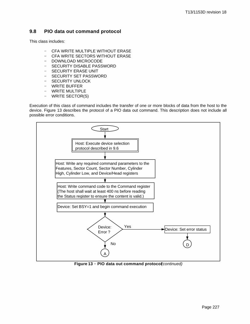
T13/1153D revision 18
Page 227
9.8 PIO data out command protocol
This class includes:
− CFA WRITE MULTIPLE WITHOUT ERASE− CFA WRITE SECTORS WITHOUT ERASE− DOWNLOAD MICROCODE− SECURITY DISABLE PASSWORD− SECURITY ERASE UNIT− SECURITY SET PASSWORD− SECURITY UNLOCK− WRITE BUFFER− WRITE MULTIPLE− WRITE SECTOR(S)
Execution of this class of command includes the transfer of one or more blocks of data from the host to thedevice. Figure 13 describes the protocol of a PIO data out command. This description does not include allpossible error conditions.
Start
Host: Write any required command parameters to theFeatures, Sector Count, Sector Number, CylinderHigh, Cylinder Low, and Device/Head registers
Host: Write command code to the Command register(The host shall wait at least 400 ns before readingthe Status register to ensure the content is valid.)
Device: Set BSY=1 and begin command execution
A
Device:Error ?
YesDevice: Set error status
DNo
Host: Execute device selection protocol described in 9.6
Figure 13 −− PIO data out command protocol (continued)

T13/1153D revision 18
Page 228
A
Device: When ready to transfer data block, set DRQ=1
Device: Clear BSY=0
Host:BSY=0 & DRQ=1?
No
Host: Read Status or Alternate Status register
Yes
Yes
No Device:All data forcommandtransferred?
Yes
No
Yes Device: Error?
Device:Set error status
Yes
Device; DRQ block transfer complete?
No
Yes
Host: Write Data register
Device: Set BSY=1 and DRQ=0
C
B
D
See 7.15.6.1
Figure 13 −− PIO data out command protocol (continued)

T13/1153D revision 18
Page 229
Device: When ready to transferdata block, set DRQ=1
B
Device: Assert INTRQ
Host: Read Status register
Device; Negate INTRQ
C
Device: Clear BSY=0
Device:nIEN=0 ?
No
Yes Host: ReadStatus register
Host:BSY=0 &DRQ=1 ?
No
Yes
NOTE −Statusregister isread to clearpendinginterupt.
Host: Read AlternateStatus register andignore results
NOTE − Thisprevents apolling host fromreading statusbefore it is valid.
Figure 13 −− PIO data out command protocol (continued)

T13/1153D revision 18
Page 230
End
Device: Assert INTRQ
Device:nIEN=0 ?
No
Yes
Host: Read Status register
Device : Negate INTRQ
Device: Clear BSY=0
D
Host: Read of Statusregister recommended
NOTE − Device: Command is complete (see 7.15.6.1 and 7.15.6.4). Host: a) Should perform its error routine if an error is reported. b) May issue another command to device. c) May select other device and issue it a command.
NOTE − Statusregister is read toclear pendinginterupt.
Host: ReadAlternate Statusregister andignore results
NOTE − Thispreventspolling hostfrom readingstatus before itis valid.
Figure 13 −− PIO data out command protocol (concluded)

T13/1153D revision 18
Page 231
9.9 Non-data command protocol
This class includes:
− CFA ERASE SECTORS− CFA REQUEST EXTENDED ERROR CODE− CHECK POWER MODE− FLUSH CACHE− GET MEDIA STATUS− IDLE− IDLE IMMEDIATE− INITIALIZE DEVICE PARAMETERS− MEDIA EJECT− MEDIA LOCK− MEDIA UNLOCK− NOP− READ NATIVE MAX ADDRESS− READ VERIFY SECTOR(S)− SECURITY ERASE PREPARE− SECURITY FREEZE LOCK− SEEK− SET FEATURES− SET MAX ADDRESS− SET MULTIPLE MODE− SLEEP− SMART DISABLE OPERATION− SMART ENABLE/DISABLE AUTOSAVE− SMART ENABLE OPERATION− SMART EXECUTE OFFLINE IMMEDIATE− SMART RETURN STATUS− STANDBY− STANDBY IMMEDIATE
Execution of these commands involves no data transfer. Figure 14 describes the protocol of a no datatransfer command. This description does not include all possible error conditions.
See the NOP command description in 0 and the SLEEP command description in 8.40 for additional protocolrequirements.
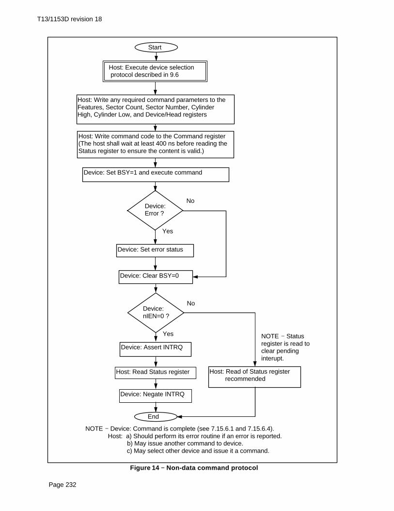
T13/1153D revision 18
Page 232
Start
Host: Write any required command parameters to theFeatures, Sector Count, Sector Number, CylinderHigh, Cylinder Low, and Device/Head registers
Host: Write command code to the Command register(The host shall wait at least 400 ns before reading theStatus register to ensure the content is valid.)
Device: Set BSY=1 and execute command
Device:Error ?
No
Yes
Device: Set error status
Host: Execute device selection protocol described in 9.6
Device:nIEN=0 ?
No
Yes
Device: Clear BSY=0
End
Device: Assert INTRQ
Host: Read Status register
Device: Negate INTRQ
Host: Read of Status register recommended
NOTE − Device: Command is complete (see 7.15.6.1 and 7.15.6.4). Host: a) Should perform its error routine if an error is reported. b) May issue another command to device. c) May select other device and issue it a command.
NOTE − Statusregister is read toclear pendinginterupt.
Figure 14 −− Non-data command protocol
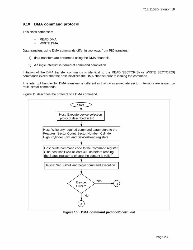
T13/1153D revision 18
Page 233
9.10 DMA command protocol
This class comprises:
− READ DMA− WRITE DMA
Data transfers using DMA commands differ in two ways from PIO transfers:
1) data transfers are performed using the DMA channel; 2) A Single interrupt is issued at command completion.
Initiation of the DMA transfer commands is identical to the READ SECTOR(S) or WRITE SECTOR(S)commands except that the host initializes the DMA channel prior to issuing the command.
The interrupt handler for DMA transfers is different in that no intermediate sector interrupts are issued onmulti-sector commands.
Figure 15 describes the protocol of a DMA command..
Start
Host: Write any required command parameters to theFeatures, Sector Count, Sector Number, CylinderHigh, Cylinder Low, and Device/Head registers
Host: Write command code to the Command register(The host shall wait at least 400 ns before readingthe Status register to ensure the content is valid.)
Device: Set BSY=1 and begin command execution
A
Device:Error ?
No
YesB
Host: Execute device selection protocol described in 9.6
Figure 15 −− DMA command protocol (continued)

T13/1153D revision 18
Page 234
A
Device: When ready to transfer data, assert DMARQ
Host: When ready to transfer data, assert DMACK-
NOTE − Transfer data asdescribed in Multiword DMAtiming or Ultra DMA protocol
Device:Transferdone?
No
Yes
Device:Error ?
No
Yes
Device: Set error status
Device: Clear BSY=0 and DRQ=0
B
Device:nIEN=0 ?
No
Yes
End
Device: Assert INTRQ
Host: Read Status register
Device: Negate INTRQ
Host: Read of Status register recommended
Device: Set BSY=1, or BSY=0 and DRQ=1
NOTE − Device: Command is complete (see 7.15.6.1 and 7.15.6.4). Host: a) Should perform its error routine if an error is reported. b) May issue another command to device. c) May select other device and issue it a command.
NOTE − Statusregister is read toclear pendinginterupt.
Figure 15 −− DMA command protocol (concluded)
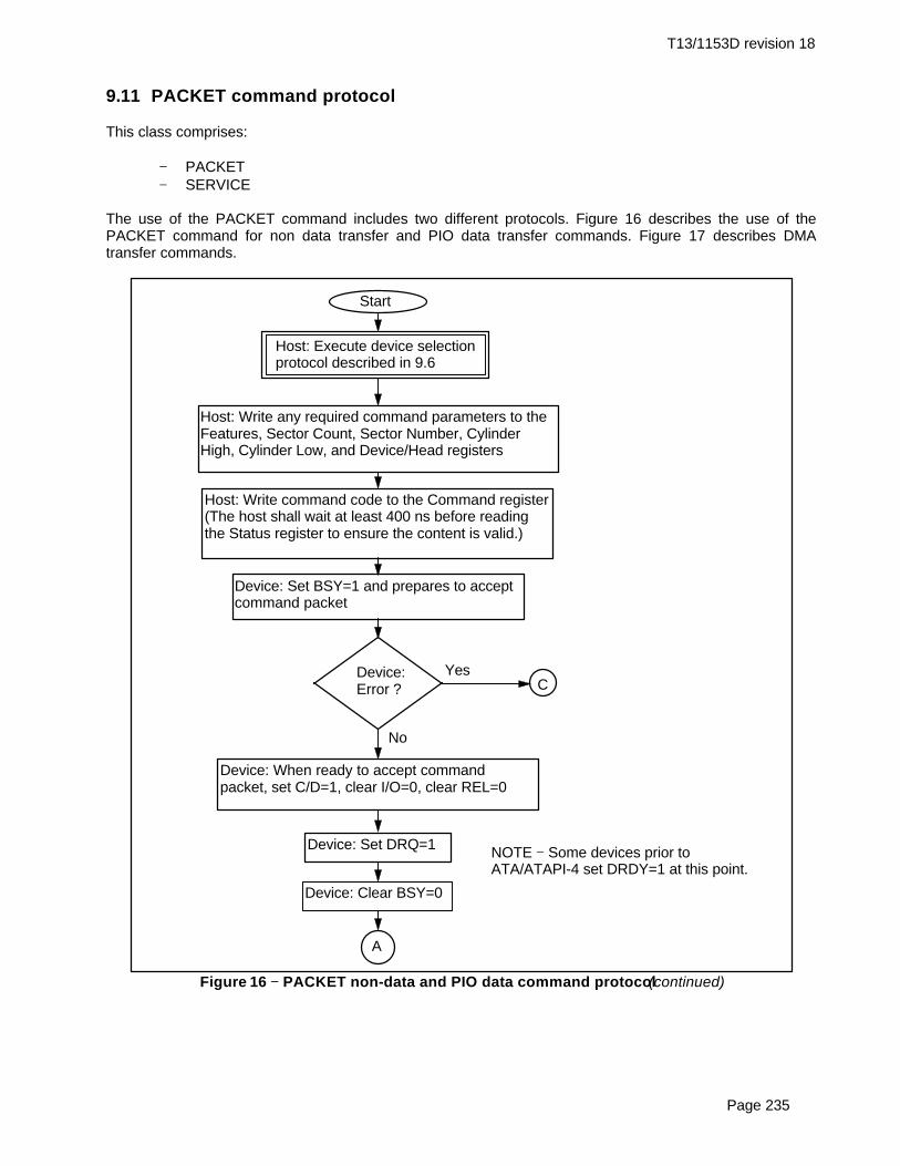
T13/1153D revision 18
Page 235
9.11 PACKET command protocol
This class comprises:
− PACKET− SERVICE
The use of the PACKET command includes two different protocols. Figure 16 describes the use of thePACKET command for non data transfer and PIO data transfer commands. Figure 17 describes DMAtransfer commands.
Start
Host: Write any required command parameters to theFeatures, Sector Count, Sector Number, CylinderHigh, Cylinder Low, and Device/Head registers
Host: Write command code to the Command register(The host shall wait at least 400 ns before readingthe Status register to ensure the content is valid.)
Device: Set BSY=1 and prepares to acceptcommand packet
Device: When ready to accept commandpacket, set C/D=1, clear I/O=0, clear REL=0
A
Host: Execute device selection protocol described in 9.6
Device:Error ?
No
YesC
Device: Set DRQ=1
Device: Clear BSY=0
NOTE − Some devices prior toATA/ATAPI-4 set DRDY=1 at this point.
Figure 16 −− PACKET non-data and PIO data command protocol (continued)
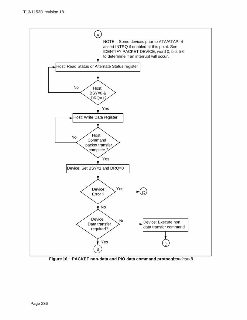
T13/1153D revision 18
Page 236
A
Host: Commandpacket transfer complete ?
No
Yes
Host: Write Data register
B
Device: Set BSY=1 and DRQ=0
Device:Error ?
No
YesC
Host:BSY=0 & DRQ=1?
No
Yes
Host: Read Status or Alternate Status register
NOTE − Some devices prior to ATA/ATAPI-4assert INTRQ if enabled at this point. SeeIDENTIFY PACKET DEVICE, word 0, bits 5-6to determine if an interrupt will occur.
Device:Data transfer required?
Yes
No
D
Device: Execute nondata transfer command
Figure 16 −− PACKET non-data and PIO data command protocol (continued)

T13/1153D revision 18
Page 237
Device: When ready to transfer data block; set Tag; bytecount; I/O=1 for data in, I/O=0 for data out; C/D=0, DRQ=1
Device: Clear BSY=0
No
Yes Device:nIEN=0 ?
Device: Assert INTRQ
Host: Read Statusregister (clear interrupt)
Device: Negate INTRQ
B
No
Yes Device:Overlap supported, enabled and OVL set ?
F
G
K
Host:BSY=0 &DRQ=1?
No
Yes
Host: Read Status register
Host: Read or write Data register
E
Device: DRQ block transfer complete ?
No
Yes
J
NOTE − Statusregister is read toclear pendinginterupt.
Host: Read AlternateStatus register and ignoreresults
NOTE − Thisprevents polling hostfrom reading statusbefore it is valid.
Figure 16 −− PACKET non-data and PIO data command protocol (continued)

T13/1153D revision 18
Page 238
E
Device: Set BSY=1
Device: Clear DRQ=0
Device:All data for commandtransferred?
Yes
No
Device: Set I/O=1, C/D=1, DRDY=1, REL=0
End
Device: Assert INTRQ
Device:nIEN=0 ?
No
Yes
Host: Read Status register
Device: Negate INTRQ
Device: Clear BSY=0
Host: Read of Status register recommended
Device:Error?
No
Yes
No
Yes
Device: Error?
Device: Set errorstatus
NOTE − Device: Command is complete (see 7.15.6.1 and 7.15.6.4). Host: a) Should perform its error routine if an error is reported. b) May issue another command to the device. c) May select other device and issue it a command.
B
CD
NOTE − Statusregister is read toclear pendinginterupt.
Host: Read AlternateStatus register andignore results
NOTE − Thisprevents pollinghost fromreading statusbefore it is valid.
Figure 16 −− PACKET non-data and PIO data command protocol (continued)

T13/1153D revision 18
Page 239
F
Device:Bus release interrupt enabled ?
No
Yes
Device: Bus release ?
No
Yes
G
Yes
No
Device:nIEN=0 ?
Device: Assert INTRQ
Host: Read Statusregister
Device: Negate INTRQ
Device: Set REL, clear I/O=0,C/D=0
Device: Clear BSY
Yes
No Device:Bus release interrupt enabled ?
H
Host:BSY=0 &DRQ=0?
No
Yes
Host: Read Status register
NOTE − Statusregister is read toclear pendinginterupt.
Host: Read Alternate Statusregister and ignore results
NOTE − Thispreventspolling hostfrom readingstatus beforeit is valid.
Figure 16 −− PACKET non-data and PIO data command protocol(continued)

T13/1153D revision 18
Page 240
HNOTE − The device has performed a bus release at this point. The host may: a) issue another command if the device supports queuing. b) select the other device and issue it commands. c) if overlapped commands are outstanding to both devices, the host may poll INTRQ by first selecting one device, then selecting the other device. See 6.6 and 6.7.
Host: Device selected?
No
Yes
Device: When ready to transferdata, set SERV=1
Host: Write Device/Head register toselect device (The host shall wait atleast 400ns before reading the Statusregister to ensure the content is valid.)
Device:nIEN=0?
No
YesDevice: Assert INTRQ
Host: Read Status register
Host: Read Status register
Host:SERV=1 & BSY=0?
No
Yes
I
Device: Negate INTRQ
NOTE − Statusregister is read toclear pendinginterupt.
Host: Read Alternate Statusregister and ignore results
NOTE − Thispreventspolling hostfrom readingstatus before itis valid.
Figure 16 −− PACKET non-data and PIO data command protocol(continued)

T13/1153D revision 18
Page 241
I
Host: Write SERVICE command (A2h) to Commandregister (The host shall wait at least 400 ns beforereading the Status register to ensure the content is valid.)
Device: Set BSY=1 and begin SERVICE execution
K
C
Device:Error ?
No
YesDevice: Set error status
Device: When ready to transfer data block; set Tag;byte count; SERV=0; C/D=0; REL=0, I/O=1 for datain, I/O=0 for data out; DRQ=1
Device: Clear BSY=0
Device: Serviceinterruptenabled?
No
Yes
J
NOTE − If another queuedcommand is ready for service,SERV shall remain equal to one.
Figure 16 −− PACKET non-data and PIO data command protocol(concluded)
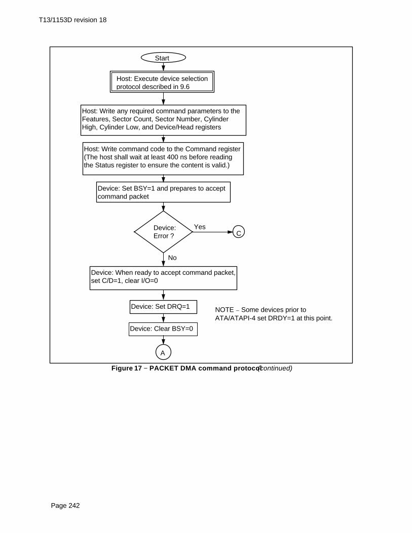
T13/1153D revision 18
Page 242
Start
Host: Write any required command parameters to theFeatures, Sector Count, Sector Number, CylinderHigh, Cylinder Low, and Device/Head registers
Host: Write command code to the Command register(The host shall wait at least 400 ns before readingthe Status register to ensure the content is valid.)
Device: Set BSY=1 and prepares to acceptcommand packet
Device: When ready to accept command packet,set C/D=1, clear I/O=0
A
Host: Execute device selection protocol described in 9.6
Device:Error ?
No
YesC
Device: Set DRQ=1
Device: Clear BSY=0
NOTE − Some devices prior toATA/ATAPI-4 set DRDY=1 at this point.
Figure 17 −− PACKET DMA command protocol(continued)

T13/1153D revision 18
Page 243
A
Host: Commandpacket transfer complete ?
No
Yes
Host: Write Data register
B
Device: Set BSY=1 and DRQ=0
Device:Error ?
No
YesC
Host:BSY=0 & DRQ=1?
No
Yes
Host: Read Status or Alternate Status register
NOTE − Some devices prior to ATA/ATAPI-4assert INTRQ if enabled at this point. SeeIDENTIFY PACKET DEVICE, word 0, bits 5-6to determine if an interrupt will occur.
Device:Data transfer required?
Yes
No
D
Device: Execute nondata transfer command
Figure 17 −− PACKET DMA command protocol (continued)

T13/1153D revision 18
Page 244
B
No
Yes Device:Overlap supported,enabled & OVL set ?
F
Device: When ready to transfer data block; I/O=1 for datain, I/O=0 for data out, C/D=0, REL=0, SERV=0, DMRD=1,DRQ=1
G
E
Device: When ready to transfer data, assert DMARQ
Host: When ready to transfer data, assert DMACK-
NOTE − Transfer data asdescribed in Multi Word DMAtiming or Ultra DMA protocol
J
Device: Clear BSY=0
NOTE − If another queuedcommand is ready for service,SERV shall remain equal toone.
Figure 17 −− PACKET DMA command protocol (continued)
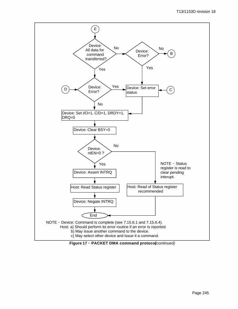
T13/1153D revision 18
Page 245
E
NOTE − Device: Command is complete (see 7.15.6.1 and 7.15.6.4). Host: a) Should perform its error routine if an error is reported. b) May issue another command to the device. c) May select other device and issue it a command.
Device:All data for commandtransferred?
Yes
No
Device: Set I/O=1, C/D=1, DRDY=1,DRQ=0
End
Device: Assert INTRQ
Device:nIEN=0 ?
No
Yes
Host: Read Status register
Device: Negate INTRQ
Device: Clear BSY=0
Host: Read of Status register recommended
Device:Error?
No
Yes
No
Yes
Device: Error?
Device: Set errorstatus
B
CD
NOTE − Statusregister is read toclear pendinginterupt.
Figure 17 −− PACKET DMA command protocol (continued)

T13/1153D revision 18
Page 246
F
Device:Bus release interrupt enabled ?
No
Yes
Device: Bus release ?
No
Yes
G
Device: Set REL=1, clear I/O=0,C/D=0
Device: Clear BSY=0
H
Host:BSY=0 &DRQ=0?
No
Yes
Yes
No
Device:nIEN=0 ?
Host: Read Status register
Device: Assert INTRQ
Host: Read Statusregister
Device: Negate INTRQ
Yes
No Device:Bus release interrupt enabled ?
NOTE − Statusregister is read toclear pendinginterrupt.
Figure 17 −− PACKET DMA command protocol (continued)

T13/1153D revision 18
Page 247
HNOTE − The device has performed a bus release at this point. The host may: a) issue another command if the device supports queuing. b) select the other device and issue it commands. c) if overlapped commands are outstanding to both devices, the host may poll INTRQ by first selecting one device, then selecting the other device. See 6.6 and 6.7.
Host: Device selected?
No
Yes
Device:nIEN=0?
No
Yes
Device: When ready to transferdata, set SERV=1
Host: Write Device/Head register toselect device (The host shall wait atleast 400ns before reading the Statusregister to ensure the content is valid.)
Device: Assert INTRQ
Host: Read Status register
Host:SERV=1 & BSY=0?
No
Yes
Host: Read Status register
I
Device: Negate INTRQ
NOTE − Statusregister is read toclear pendinginterupt.
Figure 17 −− PACKET DMA command protocol (continued)
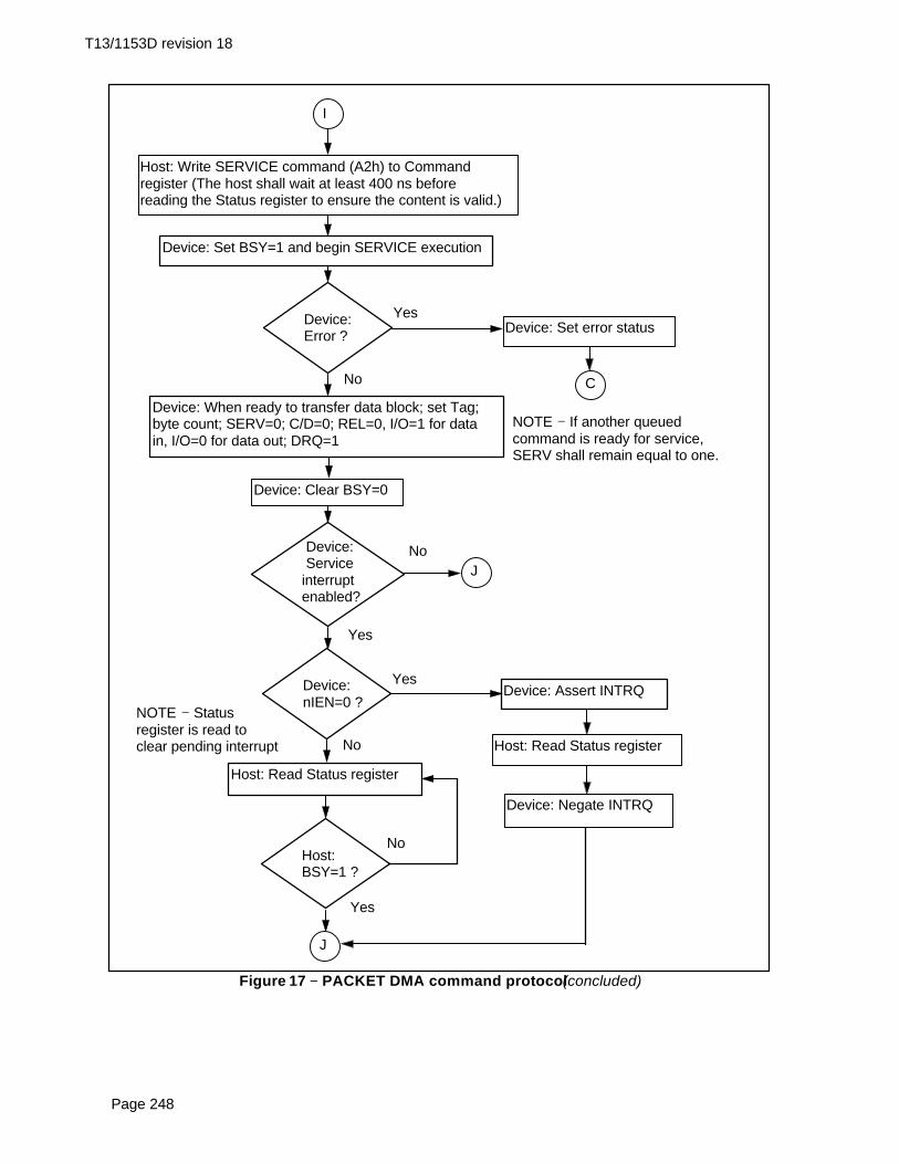
T13/1153D revision 18
Page 248
I
Host: Write SERVICE command (A2h) to Commandregister (The host shall wait at least 400 ns beforereading the Status register to ensure the content is valid.)
Device: Set BSY=1 and begin SERVICE execution
J
C
Device:Error ?
No
YesDevice: Set error status
Device: When ready to transfer data block; set Tag;byte count; SERV=0; C/D=0; REL=0, I/O=1 for datain, I/O=0 for data out; DRQ=1
Device: Clear BSY=0
Device: Serviceinterruptenabled?
No
Yes
J
Device:nIEN=0 ?
No
Yes
Host: Read Status register
Device: Assert INTRQ
Host: Read Status register
Device: Negate INTRQ
Host:BSY=1 ?
No
Yes
NOTE − Statusregister is read toclear pending interrupt
NOTE − If another queuedcommand is ready for service,SERV shall remain equal to one.
Figure 17 −− PACKET DMA command protocol (concluded)

T13/1153D revision 18
Page 249
9.12 READ/WRITE DMA QUEUED command protocol
This class includes:
− READ DMA QUEUED− SERVICE− WRITE DMA QUEUED
Figure 18 describes the execution of a READ DMA QUEUED or WRITE DMA QUEUED command.
Start
Host: Write any required command parameters to theFeatures, Sector Count, Sector Number, CylinderHigh, Cylinder Low, and Device/Head registers
Host: Write command code to the Command register(The host shall wait at least 400 ns before readingthe Status register to ensure the content is valid.)
Device: Set BSY=1 and begin command execution
A
BDevice:Error ?
Yes
No
Device:Data ready ?
Yes
NoC
Host: Execute device selection protocol described in 9.6
Device: Set Tag, SERV=0, C/D=0, I/Oappropriately, REL=0, DRQ=1
D
Device: Clear BSY=0
NOTE − If another queuedcommand is ready forservice, SERV shall remainequal to one.
Figure 18 −− READ/WRITE DMA QUEUED command protocol (continued)

T13/1153D revision 18
Page 250
A
Device: When ready to transfer data, assert DMARQ
Host: When ready to transfer data, assert DMACK-
NOTE − Transfer data asdescribed in Multi Word DMAtiming or Ultra DMA protocol
Device:Transferdone?
No
Yes
Device:Error ?
No
Yes
Device: Set error status
Device: Set Tag, SERV=0, I/O=1, C/D=1, REL=0, DRQ=0
Device Clear BSY=0
End
Device: Assert INTRQ
Device:nIEN=0 ?
No
Yes
Host: Read Status register
Device: Negate INTRQ
Host: Read of Status register recommended
B
NOTE − Status registeris read to clear pendinginterrupt
NOTE − Device: Command is complete (see 7.15.6.1 and 7.15.6.4). Host: a) Should perform its error routine if an error is reported. b) May issue another command to device. c) May select other device and issue it a comand.
NOTE − When DMARQ has been asserted at leastone data word shall be transferred.
NOTE − If another queuedcommand is ready forservice, SERV shall remainequal to one.
Figure 18 −− READ/WRITE DMA QUEUED command protocol (continued)

T13/1153D revision 18
Page 251
Device: Set REL=1, I/O=0, C/D=0
C
Device: Clear BSY=0
NOTE − The device has performed a bus release. The host may: a) issue another command if the device supports queuing. b) select the other device and issue it commands. c) if overlapped commands are outstanding to both devices, the host may poll INTRQ by first selecting one device, then selecting the other device. See 6.6 and 6.7.
E
Host:BSY=0 &DRQ=0?
No
Yes
Yes
No
Device:nIEN=0 ?
Host: Read Status register
Device: Assert INTRQ
Host: Read Statusregister
Device: Negate INTRQ
Yes
No Device:Bus release interrupt enabled ?
NOTE − Statusregister is read toclear pendinginterrupt.
Figure 18 −− READ/WRITE DMA QUEUED command protocol (continued)

T13/1153D revision 18
Page 252
Host: Write SERVICE command (A2h) to Commandregister (The host shall wait at least 400 ns beforereading the Status register to ensure the content is valid.)
Device: Set BSY=1 and begin SERVICE execution
D
Host:Deviceselected?
No
Yes
E
Device:nIEN=0?
No
Yes
Device: When ready to transferdata, set SERV=1
Host: Write Device/Head register toselect device (The host shall wait atleast 400 ns before reading the Statusregister to ensure the content is valid.)
Device: Assert INTRQ
Host: Read Status register
Host:BSY=0?
No
Yes
Host: Read Status register
Device: Negate INTRQ
NOTE − Statusregister is read toclear pendinginterrupt
Figure 18 −− READ/WRITE DMA QUEUED command protocol (concluded)

T13/1153D revision 18
Page 253
9.13 Ultra DMA data in commands
9.13.1 Initiating an Ultra DMA data in burst
The following steps shall occur in the order they are listed unless otherwise specifically allowed (see10.2.4.1 and 10.2.4.2 for specific timing requirements):
a) The host shall keep DMACK- in the negated state before an Ultra DMA burst is initiated.b) The device shall assert DMARQ to initiate an Ultra DMA burst. After assertion of DMARQ the device
shall not negate DMARQ until after the first negation of DSTROBE.c) Steps (c), (d), and (e) may occur in any order or at the same time. The host shall assert STOP.d) The host shall negate HDMARDY-.e) The host shall negate CS0-, CS1-, DA2, DA1, and DA0. The host shall keep CS0-, CS1-, DA2, DA1,
and DA0 negated until after negating DMACK- at the end of the burst.f) Steps (c), (d), and (e) shall have occurred at least tACK before the host asserts DMACK-. The host shall
keep DMACK- asserted until the end of an Ultra DMA burst.g) The host shall release DD(15:0) within tAZ after asserting DMACK-.h) The device may assert DSTROBE tZIORDY after the host has asserted DMACK-. Once the device has
driven DSTROBE the device shall not release DSTROBE until after the host has negated DMACK- atthe end of an Ultra DMA burst.
i) The host shall negate STOP and assert HDMARDY- within tENV after asserting DMACK-. After negatingSTOP and asserting HDMARDY-, the host shall not change the state of either signal until after receivingthe first transition of DSTROBE from the device (i.e., after the first data word has been received).
j) The device shall drive DD(15:0) no sooner than tZAD after the host has asserted DMACK-, negatedSTOP, and asserted HDMARDY-.
k) The device shall drive the first word of the data transfer onto DD(15:0). This step may occur when thedevice first drives DD(15:0) in step (j).
l) To transfer the first word of data the device shall negate DSTROBE within tFS after the host has negatedSTOP and asserted HDMARDY-. The device shall negate DSTROBE no sooner than tDVS after drivingthe first word of data onto DD(15:0).
9.13.2 The data in transfer
The following steps shall occur in the order they are listed unless otherwise specifically allowed (see10.2.4.3 and 10.2.4.2):
a) The device shall drive a data word onto DD(15:0).b) The device shall generate a DSTROBE edge to latch the new word no sooner than tDVS after changing
the state of DD(15:0). The device shall generate a DSTROBE edge no more frequently than tCYC for theselected Ultra DMA mode. The device shall not generate two rising or two falling DSTROBE edgesmore frequently than 2tcyc for the selected Ultra DMA mode.
c) The device shall not change the state of DD(15:0) until at least tDVH after generating a DSTROBE edgeto latch the data.
d) The device shall repeat steps (a), (b), and (c) until the data transfer is complete or an Ultra DMA burst ispaused, whichever occurs first.
9.13.3 Pausing an Ultra DMA data in burst
The following steps shall occur in the order they are listed unless otherwise specifically allowed (see10.2.4.4 and 10.2.4.2 for specific timing requirements).
9.13.3.1 Device pausing an Ultra DMA data in burst
a) The device shall not pause an Ultra DMA burst until at least one data word of an Ultra DMA burst hasbeen transferred.
b) The device shall pause an Ultra DMA burst by not generating DSTROBE edges.

T13/1153D revision 18
Page 254
c) NOTE − The host shall not immediately assert STOP to initiate Ultra DMA burst termination when thedevice stops generating STROBE edges. If the device does not negate DMARQ, in order to initiateULTRA DMA burst termination, the host shall negate HDMARDY- and wait tRP before asserting STOP.
d) The device shall resume an Ultra DMA burst by generating a DSTROBE edge.
9.13.3.2 Host pausing an Ultra DMA data in burst
a) The host shall not pause an Ultra DMA burst until at least one data word of an Ultra DMA burst has beentransferred.
b) The host shall pause an Ultra DMA burst by negating HDMARDY-.c) The device shall stop generating DSTROBE edges within tRFS of the host negating HDMARDY-.d) If the host negates HDMARDY- within tSR after the device has generated a DSTROBE edge, then the
host shall be prepared to receive zero or one additional data words. If the host negates HDMARDY-greater than tSR after the device has generated a DSTROBE edge, then the host shall be prepared toreceive zero, one or two additional data words. The additional data words are a result of cable roundtrip delay and tRFS timing for the device.
e) The host shall resume an Ultra DMA burst by asserting HDMARDY-.
9.13.4 Terminating an Ultra DMA data in burst
9.13.4.1 Device terminating an Ultra DMA data in burst
The following steps shall occur in the order they are listed unless otherwise specifically allowed (see10.2.4.5 and 10.2.4.2 for specific timing requirements):
a) The device shall initiate termination of an Ultra DMA burst by not generating DSTROBE edges.b) The device shall negate DMARQ no sooner than tSS after generating the last DSTROBE edge. The
device shall not assert DMARQ again until after the Ultra DMA burst is terminated.c) The device shall release DD(15:0) no later than t AZ after negating DMARQ.d) The host shall assert STOP within tLI after the device has negated DMARQ. The host shall not negate
STOP again until after the Ultra DMA burst is terminated.e) The host shall negate HDMARDY- within tLI after the device has negated DMARQ. The host shall
continue to negate HDMARDY- until the Ultra DMA burst is terminated. Steps (d) and (e) may occur atthe same time.
f) The host shall drive DD(15:0) no sooner than tZAH after the device has negated DMARQ. For this step,the host may first drive DD(15:0) with the result of its CRC calculation (see 9.15);
g) If DSTROBE is negated, the device shall assert DSTROBE within tLI after the host has asserted STOP.No data shall be transferred during this assertion. The host shall ignore this transition on DSTROBE.DSTROBE shall remain asserted until the Ultra DMA burst is terminated.
h) If the host has not placed the result of its CRC calculation on DD(15:0) since first driving DD(15:0)during (f), the host shall place the result of its CRC calculation on DD(15:0) (see 9.15).
i) The host shall negate DMACK- no sooner than tMLI after the device has asserted DSTROBE andnegated DMARQ and the host has asserted STOP and negated HDMARDY-, and no sooner than tDVSafter the host places the result of its CRC calculation on DD(15:0).
j) The device shall latch the host’s CRC data from DD(15:0) on the negating edge of DMACK-.k) The device shall compare the CRC data received from the host with the results of its own CRC
calculation. If a miscompare error occurs during one or more Ultra DMA bursts for any one command,at the end of the command the device shall report the first error that occurred (see 9.15).
l) The device shall release DSTROBE within t IORDYZ after the host negates DMACK-.m) The host shall not negate STOP nor assert HDMARDY- until at least tACK after negating DMACK-.n) The host shall not assert DIOR-, CS0-, CS1-, DA2, DA1, or DA0 until at least tACK after negating
DMACK.
9.13.4.2 Host terminating an Ultra DMA data in burst
The following steps shall occur in the order they are listed unless otherwise specifically allowed (see10.2.4.6 and 10.2.4.2 for specific timing requirements):

T13/1153D revision 18
Page 255
a) The host shall not initiate Ultra DMA burst termination until at least one data word of an Ultra DMA bursthas been transferred.
b) The host shall initiate Ultra DMA burst termination by negating HDMARDY-. The host shall continue tonegate HDMARDY- until the Ultra DMA burst is terminated.
c) The device shall stop generating DSTROBE edges within tRFS of the host negating HDMARDY-.d) If the host negates HDMARDY- within tSR after the device has generated a DSTROBE edge, then the
host shall be prepared to receive zero or one additional data words. If the host negates HDMARDY-greater than tSR after the device has generated a DSTROBE edge, then the host shall be prepared toreceive zero, one or two additional data words. The additional data words are a result of cable roundtrip delay and tRFS timing for the device.
e) The host shall assert STOP no sooner than tRP after negating HDMARDY-. The host shall not negateSTOP again until after the Ultra DMA burst is terminated.
f) The device shall negate DMARQ within tLI after the host has asserted STOP. The device shall not assertDMARQ again until after the Ultra DMA burst is terminated.
g) If DSTROBE is negated, the device shall assert DSTROBE within tLI after the host has asserted STOP.No data shall be transferred during this assertion. The host shall ignore this transition on DSTROBE.DSTROBE shall remain asserted until the Ultra DMA burst is terminated.
h) The device shall release DD(15:0) no later than t AZ after negating DMARQ.i) The host shall drive DD(15:0) no sooner than tZAH after the device has negated DMARQ. For this step,
the host may first drive DD(15:0) with the result of its CRC calculation (see 9.15).j) If the host has not placed the result of its CRC calculation on DD(15:0) since first driving DD(15:0)
during (9), the host shall place the result of its CRC calculation on DD(15:0) (see 9.15).k) The host shall negate DMACK- no sooner than tMLI after the device has asserted DSTROBE and
negated DMARQ and the host has asserted STOP and negated HDMARDY-, and no sooner than tDVSafter the host places the result of its CRC calculation on DD(15:0).
l) The device shall latch the host’s CRC data from DD(15:0) on the negating edge of DMACK-.m) The device shall compare the CRC data received from the host with the results of its own CRC
calculation. If a miscompare error occurs during one or more Ultra DMA burst for any one command, atthe end of the command, the device shall report the first error that occurred (see 9.15) .
n) The device shall release DSTROBE within t IORDYZ after the host negates DMACK-.o) The host shall neither negate STOP nor assert HDMARDY- until at least tACK after the host has negated
DMACK-.p) The host shall not assert DIOR-, CS0-, CS1-, DA2, DA1, or DA0 until at least tACK after negating
DMACK.
9.14 Ultra DMA data out commands
9.14.1 Initiating an Ultra DMA data out burst
The following steps shall occur in the order they are listed unless otherwise specifically allowed (see10.2.4.7 and 10.2.4.2 for specific timing requirements):
a) The host shall keep DMACK- in the negated state before an Ultra DMA burst is initiated.b) The device shall assert DMARQ to initiate an Ultra DMA burst.c) Steps (c), (d), and (e) may occur in any order or at the same time. The host shall assert STOP.d) The host shall assert HSTROBE.e) The host shall negate CS0-, CS1-, DA2, DA1, and DA0. The host shall keep CS0-, CS1-, DA2, DA1,
and DA0 negated until after negating DMACK- at the end of the burst.f) Steps (c), (d), and (e) shall have occurred at least tACK before the host asserts DMACK-. The host shall
keep DMACK- asserted until the end of an Ultra DMA burst.g) The device may negate DDMARDY- tZIORDY after the host has asserted DMACK-. Once the device has
negated DDMARDY-, the device shall not release DDMARDY- until after the host has negated DMACK-at the end of an Ultra DMA burst.
h) The host shall negate STOP within tENV after asserting DMACK-. The host shall not assert STOP untilafter the first negation of HSTROBE.
i) The device shall assert DDMARDY- within tLI after the host has negated STOP. After assertingDMARQ and DDMARDY- the device shall not negate either signal until after the first negation ofHSTROBE by the host.

T13/1153D revision 18
Page 256
j) The host shall drive the first word of the data transfer onto DD(15:0). This step may occur any timeduring Ultra DMA burst initiation.
k) To transfer the first word of data: the host shall negate HSTROBE no sooner than tUI after the devicehas asserted DDMARDY-. The host shall negate HSTROBE no sooner than tDVS after the driving thefirst word of data onto DD(15:0).
9.14.2 The data out transfer
The following steps shall occur in the order they are listed unless otherwise specifically allowed (see10.2.4.8 and 10.2.4.2 for specific timing requirements):
a) The host shall drive a data word onto DD(15:0).b) The host shall generate an HSTROBE edge to latch the new word no sooner than tDVS after changing the
state of DD(15:0). The host shall generate an HSTROBE edge no more frequently than tCYC for theselected Ultra DMA mode. The host shall not generate two rising or falling HSTROBE edges morefrequently than 2tcyc for the selected Ultra DMA mode.
c) The host shall not change the state of DD(15:0) until at least tDVH after generating an HSTROBE edge tolatch the data.
d) The host shall repeat steps (a), (b), and (c) until the data transfer is complete or an Ultra DMA burst ispaused, whichever occurs first.
9.14.3 Pausing an Ultra DMA data out burst
The following steps shall occur in the order they are listed unless otherwise specifically allowed (see10.2.4.9 and 10.2.4.2 for specific timing requirements).
9.14.3.1 Host pausing an Ultra DMA data out burst
a) The host shall not pause an Ultra DMA burst until at least one data word of an Ultra DMA burst has beentransferred.
b) The host shall pause an Ultra DMA burst by not generating an HSTROBE edge. NOTE − The device shall not immediately negate DMARQ to initiate Ultra DMA burst
termination when the host stops generating HSTROBE edges. If the host does not assertSTOP, in order to initiate Ultra DMA burst termination, the device shall negate DDMARDY- andwait tRP before negating DMARQ.
c) The host shall resume an Ultra DMA burst by generating an HSTROBE edge.
9.14.3.2 Device pausing an Ultra DMA data out burst
a) The device shall not pause an Ultra DMA burst until at least one data word of an Ultra DMA burst hasbeen transferred.
b) The device shall pause an Ultra DMA burst by negating DDMARDY-.c) The host shall stop generating HSTROBE edges within tRFS of the device negating DDMARDY-.d) If the device negates DDMARDY- within tSR after the host has generated an HSTROBE edge, then the
device shall be prepared to receive zero or one additional data words. If the device negatesDDMARDY- greater than tSR after the host has generated an HSTROBE edge, then the device shall beprepared to receive zero, one or two additional data words. The additional data words are a result ofcable round trip delay and tRFS timing for the host.
e) The device shall resume an Ultra DMA burst by asserting DDMARDY-.
9.14.4 Terminating an Ultra DMA data out burst
9.14.4.1 Host terminating an Ultra DMA data out burst
The following steps shall occur in the order they are listed unless otherwise specifically allowed (see10.2.4.10 and 10.2.4.2 for specific timing requirements):

T13/1153D revision 18
Page 257
a) The host shall initiate termination of an Ultra DMA burst by not generating HSTROBE edges.b) The host shall assert STOP no sooner than tSS after it last generated an HSTROBE edge. The host
shall not negate STOP again until after the Ultra DMA burst is terminated.c) The device shall negate DMARQ within tLI after the host asserts STOP. The device shall not assert
DMARQ again until after the Ultra DMA burst is terminated.d) The device shall negate DDMARDY- within tLI after the host has negated STOP. The device shall not
assert DDMARDY- again until after the Ultra DMA burst termination is complete.e) If HSTROBE is negated, the host shall assert HSTROBE within tLI after the device has negated
DMARQ. No data shall be transferred during this assertion. The device shall ignore this transition onHSTROBE. HSTROBE shall remain asserted until the Ultra DMA burst is terminated.
f) The host shall place the result of its CRC calculation on DD(15:0) (see 9.15).g) The host shall negate DMACK- no sooner than tMLI after the host has asserted HSTROBE and STOP
and the device has negated DMARQ and DDMARDY-, and no sooner than tDVS after placing the result ofits CRC calculation on DD(15:0).
h) The device shall latch the host’s CRC data from DD(15:0) on the negating edge of DMACK-.i) The device shall compare the CRC data received from the host with the results of its own CRC
calculation. If a miscompare error occurs during one or more Ultra DMA bursts for any one command,at the end of the command, the device shall report the first error that occurred (see 9.15).
j) The device shall release DDMARDY- within t IORDYZ after the host has negated DMACK-.k) The host shall neither negate STOP nor negate HSTROBE until at least tACK after negating DMACK-.l) The host shall not assert DIOW-, CS0-, CS1-, DA2, DA1, or DA0 until at least tACK after negating
DMACK.
9.14.4.2 Device terminating an Ultra DMA data out burst
The following steps shall occur in the order they are listed unless otherwise specifically allowed (see10.2.4.11 and 10.2.4.2 for specific timing requirements):
a) The device shall not initiate Ultra DMA burst termination until at least one data word of an Ultra DMAburst has been transferred.
b) The device shall initiate Ultra DMA burst termination by negating DDMARDY-.c) The host shall stop generating an HSTROBE edges within tRFS of the device negating DDMARDY-.d) If the device negates DDMARDY- within tSR after the host has generated an HSTROBE edge, then the
device shall be prepared to receive zero or one additional data words. If the device negatesDDMARDY- greater than tSR after the host has generated an HSTROBE edge, then the device shall beprepared to receive zero, one or two additional data words. The additional data words are a result ofcable round trip delay and tRFS timing for the host.
e) The device shall negate DMARQ no sooner than tRP after negating DDMARDY-. The device shall notassert DMARQ again until after the Ultra DMA burst is terminated.
f) The host shall assert STOP within tLI after the device has negated DMARQ. The host shall not negateSTOP again until after the Ultra DMA burst is terminated.
g) If HSTROBE is negated, the host shall assert HSTROBE within tLI after the device has negatedDMARQ. No data shall be transferred during this assertion. The device shall ignore this transition ofHSTROBE. HSTROBE shall remain asserted until the Ultra DMA burst is terminated.
h) The host shall place the result of its CRC calculation on DD(15:0) (see 9.15).i) The host shall negate DMACK- no sooner than tMLI after the host has asserted HSTROBE and STOP
and the device has negated DMARQ and DDMARDY-, and no sooner than tDVS after placing the result ofits CRC calculation on DD(15:0).
j) The device shall latch the host’s CRC data from DD(15:0) on the negating edge of DMACK-.k) The device shall compare the CRC data received from the host with the results of its own CRC
calculation. If a miscompare error occurs during one or more Ultra DMA bursts for any one command,at the end of the command, the device shall report the first error that occurred (see 9.15).
l) The device shall release DDMARDY- within t IORDYZ after the host has negated DMACK-.m) The host shall neither negate STOP nor HSTROBE until at least tACK after negating DMACK-.n) The host shall not assert DIOW-, CS0-, CS1-, DA2, DA1, or DA0 until at least tACK after negating
DMACK.

T13/1153D revision 18
Page 258
9.15 Ultra DMA CRC rules
The following is a list of rules for calculating CRC, determining if a CRC error has occurred during an UltraDMA burst, and reporting any error that occurs at the end of a command.
1) Both the host and the device shall have a 16-bit CRC calculation function.2) Both the host and the device shall calculate a CRC value for each Ultra DMA burst.3) The CRC function in the host and the device shall be initialized with a seed of 4ABAh at the beginning
of an Ultra DMA burst before any data is transferred.4) For each STROBE transition used for data transfer, both the host and the device shall calculate a new
CRC value by applying the CRC polynomial to the current value of their individual CRC functions andthe word being transferred. CRC is not calculated for the return of STROBE to the asserted state afterthe Ultra DMA burst termination request has been acknowledged.
5) At the end of any Ultra DMA burst the host shall send the results of its CRC calculation function to thedevice on DD(15:0) with the negation of DMACK-.
6) The device shall then compare the CRC data from the host with the calculated value in its own CRCcalculation function. If the two values do not match, the device shall save the error and report it at theend of the command. A subsequent Ultra DMA burst for the same command that does not have a CRCerror shall not clear an error saved from a previous Ultra DMA burst in the same command. If amiscompare error occurs during one or more Ultra DMA bursts for any one command, at the end of thecommand, the device shall report the first error that occurred.
7) For READ DMA, WRITE DMA, READ DMA QUEUED, or WRITE DMA QUEUED commands: When aCRC error is detected, it shall be reported by setting both ICRC and ABRT (bit 7 and bit 2 in the Errorregister) to one. ICRC is defined as the “Interface CRC Error” bit. The host shall respond to this error byre-issuing the command.
8) For a REQUEST SENSE packet command (see SPC T10/955D for definition of the REQUEST SENSEcommand): When a CRC error is detected during transmission of sense data the device shall completethe command and set CHK to one. The device shall report a Sense key of 0Bh (ABORTEDCOMMAND). The device shall preserve the original sense data that was being returned when the CRCerror occurred. The device shall not report any additional sense data specific to the CRC error. Thehost device driver may retry the REQUEST SENSE command or may consider this an unrecoverableerror and retry the command that caused the Check Condition.
9) For any packet command except a REQUEST SENSE command: If a CRC error is detected, thedevice shall complete the command with CHK set to one. The device shall report a Sense key of 04h(HARDWARE ERROR). The sense data supplied via a subsequent REQUEST SENSE command shallreport an ASC/ASCQ value of 08h/03h (LOGICAL UNIT COMMUNICATION CRC ERROR). Hostdrivers should retry the command that resulted in a HARDWARE ERROR.
NOTE − If excessive CRC errors are encountered while operating in Ultra mode 2 or 1, thehost should select a slower Ultra mode. Caution: CRC errors are detected and reported onlywhile operating in an Ultra mode.
10) A host may send extra data words on the last Ultra DMA burst of a data out command. If a device
determines that all data has been transferred for a command, the device shall terminate the burst. Adevice may have already received more data words than were required for the command. These extrawords are used by both the host and the device to calculate the CRC, but, on an Ultra DMA data outburst, the extra words shall be discarded by the device.
11) The CRC generator polynomial is: G(X) = X16 + X12 + X5 + 1. Table 28 describes the equations for 16-bit parallel generation of the resulting polynomial (based on a word boundary).
NOTE − Since no bit clock is available, the recommended approach for calculating CRC isto use a word clock derived from the bus strobe. The combinational logic is then equivalentto shifting sixteen bits serially through the generator polynomial where DD0 is shifted in firstand DD15 is shifted in last.
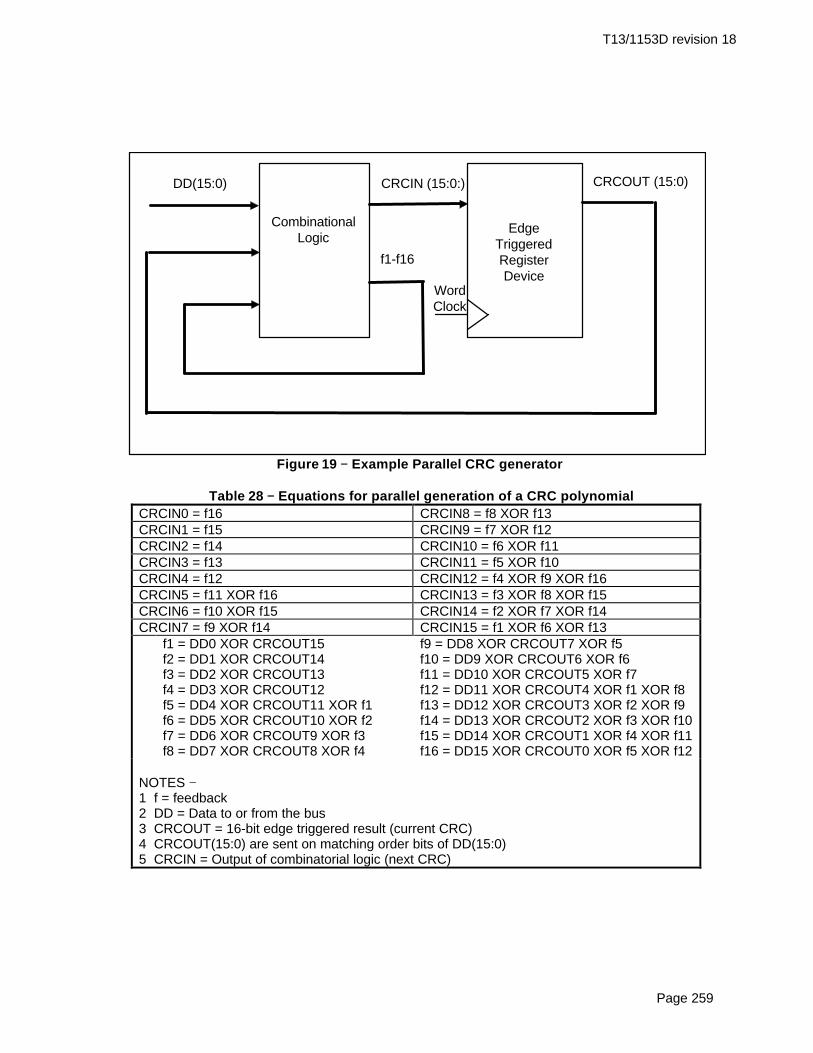
T13/1153D revision 18
Page 259
CombinationalLogic
EdgeTriggeredRegisterDevice
CRCOUT (15:0)CRCIN (15:0:)DD(15:0)
f1-f16
WordClock
Figure 19 −− Example Parallel CRC generator
Table 28 −− Equations for parallel generation of a CRC polynomialCRCIN0 = f16 CRCIN8 = f8 XOR f13CRCIN1 = f15 CRCIN9 = f7 XOR f12CRCIN2 = f14 CRCIN10 = f6 XOR f11CRCIN3 = f13 CRCIN11 = f5 XOR f10CRCIN4 = f12 CRCIN12 = f4 XOR f9 XOR f16CRCIN5 = f11 XOR f16 CRCIN13 = f3 XOR f8 XOR f15CRCIN6 = f10 XOR f15 CRCIN14 = f2 XOR f7 XOR f14CRCIN7 = f9 XOR f14 CRCIN15 = f1 XOR f6 XOR f13
f1 = DD0 XOR CRCOUT15f2 = DD1 XOR CRCOUT14f3 = DD2 XOR CRCOUT13f4 = DD3 XOR CRCOUT12f5 = DD4 XOR CRCOUT11 XOR f1f6 = DD5 XOR CRCOUT10 XOR f2f7 = DD6 XOR CRCOUT9 XOR f3f8 = DD7 XOR CRCOUT8 XOR f4
f9 = DD8 XOR CRCOUT7 XOR f5f10 = DD9 XOR CRCOUT6 XOR f6f11 = DD10 XOR CRCOUT5 XOR f7f12 = DD11 XOR CRCOUT4 XOR f1 XOR f8f13 = DD12 XOR CRCOUT3 XOR f2 XOR f9f14 = DD13 XOR CRCOUT2 XOR f3 XOR f10f15 = DD14 XOR CRCOUT1 XOR f4 XOR f11f16 = DD15 XOR CRCOUT0 XOR f5 XOR f12
NOTES −1 f = feedback2 DD = Data to or from the bus3 CRCOUT = 16-bit edge triggered result (current CRC)4 CRCOUT(15:0) are sent on matching order bits of DD(15:0)5 CRCIN = Output of combinatorial logic (next CRC)

T13/1153D revision 18
Page 260
9.16 Single device configurations
9.16.1 Device 0 only configurations
In a single device configuration where Device 0 is the only device and the host selects Device 1, Device 0shall respond as follows:
1) A write to the Device Control register shall complete as if Device 0 was the selected device;2) A write to a Command Block register, other than the Command register, shall complete as if
Device 0 was selected;3) A write to the Command register shall be ignored, except for EXECUTE DEVICE DIAGNOSTIC;4) A read of the Control Block or Command Block registers, other than the Status or Alternate
Status registers, shall complete as if Device 0 was selected;5) A read of the Status or Alternate status register shall return the value 00h.
NOTE − Even though Device 1 is not present, the register content may appear valid forDevice 1. Further means may be necessary to determine the existence of Device 1, e.g.,issuing a command.
9.16.2 Device 1 only configurations
Host support of Device 1 only configurations is host specific.
In a single device configuration where Device 1 is the only device and the host selects Device 0, Device 1shall respond to accesses of the Command Block and Control Block registers in the same way it would ifDevice 0 was present. This is because Device 1 cannot determine if Device 0 is, or is not, present.
Host implementation of read and write operations to the Command and Control Block registers of non-existent Device 0 are host specific.
NOTE − The remainder of this section is a host implementation note. The host implementorshould be aware of the following when supporting Device 1 only configurations:
1) Following a hardware reset or software reset, Device 1 will not be selected. The followingsteps may be used to reselect Device 1:
a) Write to the Device/Head register with DEV bit set to one;b) Using one or more of the Command Block registers that may be both written and
read, such as the Sector Count or Sector Number, write a data pattern other than00h or FFh to the register(s);
c) Read the register(s) written in step (b). If the data read is the same as the datawritten, proceed to step (e);
d) Repeat steps (a) to (c) until the data matches in step (c) or until 31 s has past.After 31 s it may probably be assumed that Device 1 is not functioning properly;
e) Read the Status register and Error registers. Check the Status and Error registercontents for any error conditions that Device 1 may have posted.
2) Following the execution of an EXECUTE DEVICE DIAGNOSTIC command, Device 1 willnot be selected. Also, no interrupt will be generated to signal command completion. Afterwriting the EXECUTE DEVICE DIAGNOSTIC command to the Command register,execute steps (a) to (e) as described in (1) above;
3) At all other times, do not write zero into the DEV bit of the Device/Head register. All othercommands execute normally.

T13/1153D revision 18
Page 261
10 Timing
10.1 Deskewing
The host shall provide cable deskewing for all signals originating from the device. The device shall providecable deskewing for all signals originating at the host.
All timing values and diagrams are shown and measured at the connector of the selected device.
10.2 Transfer timing
The minimum cycle time supported by the device in PIO mode 3, 4 and Multiword DMA mode 1, 2respectively shall always be greater than or equal to the minimum cycle time defined by the associatedmode e.g., a device supporting PIO mode 4 timing shall not report a value less than 120 ns, the minimumcycle time defined for PIO mode 4 timings.
See 3.2.6 for timing diagram conventions.
10.2.1 Register transfers
Figure 20 defines the relationships between the interface signals for register transfers. Peripherals reportingsupport for PIO mode 3 or 4 shall power up in a PIO mode 0, 1, or 2.
For PIO modes 3 and above, the minimum value of t0 is specified by word 68 in the IDENTIFY DEVICEparameter list. Table 29 defines the minimum value that shall be placed in word 68.
IORDY shall be supported when PIO mode 3 or 4 are the current mode of operation.
NOTE − Some devices implementing the PACKET Command feature set prior to thisstandard power up in PIO mode 3 and enable IORDY as the default.

T13/1153D revision 18
Page 262
t 0
ADDR valid (See note 1) t 1 t 2 t 9
t 2i
DIOR-/DIOW-
WRITE DD(7:0) (See note 2) t 3 t4
READ DD(7:0) (See note 2) t 5 t6
t 6z
IORDY (See note 3,3-1) t A
IORDY (See note 3,3-2) t C
t RD
IORDY (See note 3,3-3) t B tC
NOTES − 1 Device address consists of signals CS0-, CS1- and DA(2:0) 2 Data consists of DD(7:0). 3 The negation of IORDY by the device is used to extend the PIO cycle. The determination of whether the
cycle is to be extended is made by the host after t A from the assertion of DIOR- or DIOW-. Theassertion and negation of IORDY are described in the following three cases:3-1 Device never negates IORDY, devices keeps IORDY released: no wait is generated.3-2 Device negates IORDY before t A, but causes IORDY to be asserted before t A. IORDY is releasedprior to negation and may be asserted for no more than 5 ns before release: no wait generated.3-3 Device negates IORDY before t A. IORDY is released prior to negation and may be asserted for nomore than 5 ns before release: wait generated. The cycle completes after IORDY is reasserted. Forcycles where a wait is generated and DIOR- is asserted, the device shall place read data on DD(7:0)for tRD before asserting IORDY.
Figure 20 −− Register transfer to/from device
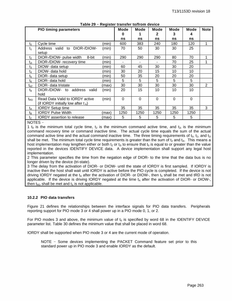
T13/1153D revision 18
Page 263
Table 29 −− Register transfer to/from devicePIO timing parameters Mode
0ns
Mode1
ns
Mode2
ns
Mode3
ns
Mode4
ns
Note
t0 Cycle time (min) 600 383 240 180 120 1t1 Address valid to DIOR-/DIOW-
setup(min) 70 50 30 30 25
t2 DIOR-/DIOW- pulse width 8-bit (min) 290 290 290 80 70 1t2i DIOR-/DIOW- recovery time (min) - - - 70 25 1t3 DIOW- data setup (min) 60 45 30 30 20t4 DIOW- data hold (min) 30 20 15 10 10t5 DIOR- data setup (min) 50 35 20 20 20t6 DIOR- data hold (min) 5 5 5 5 5t6Z DIOR- data tristate (max) 30 30 30 30 30 2t9 DIOR-/DIOW- to address valid
hold(min) 20 15 10 10 10
tRD Read Data Valid to IORDY active(if IORDY initially low after t A)
(min) 0 0 0 0 0
tA IORDY Setup time 35 35 35 35 35 3tB IORDY Pulse Width (max) 1250 1250 1250 1250 1250tC IORDY assertion to release (max) 5 5 5 5 5
NOTES −1 t0 is the minimum total cycle time, t2 is the minimum command active time, and t2i is the minimumcommand recovery time or command inactive time. The actual cycle time equals the sum of the actualcommand active time and the actual command inactive time. The three timing requirements of t0, t2, and t2ishall be met. The minimum total cycle time requirements is greater than the sum of t2 and t2i. This means ahost implementation may lengthen either or both t2 or t2i to ensure that t0 is equal to or greater than the valuereported in the devices IDENTIFY DEVICE data. A device implementation shall support any legal hostimplementation.2 This parameter specifies the time from the negation edge of DIOR- to the time that the data bus is nolonger driven by the device (tri-state).3 The delay from the activation of DIOR- or DIOW- until the state of IORDY is first sampled. If IORDY isinactive then the host shall wait until IORDY is active before the PIO cycle is completed. If the device is notdriving IORDY negated at the tA after the activation of DIOR- or DIOW-, then t5 shall be met and tRD is notapplicable. If the device is driving IORDY negated at the time tA after the activation of DIOR- or DIOW-,then tRD shall be met and t5 is not applicable.
10.2.2 PIO data transfers
Figure 21 defines the relationships between the interface signals for PIO data transfers. Peripheralsreporting support for PIO mode 3 or 4 shall power up in a PIO mode 0, 1, or 2.
For PIO modes 3 and above, the minimum value of t0 is specified by word 68 in the IDENTIFY DEVICEparameter list. Table 30 defines the minimum value that shall be placed in word 68.
IORDY shall be supported when PIO mode 3 or 4 are the current mode of operation.
NOTE − Some devices implementing the PACKET Command feature set prior to thisstandard power up in PIO mode 3 and enable IORDY as the default.

T13/1153D revision 18
Page 264
t 0
ADDR valid (See note 1) t 1 t 2 t 9
t 2i
DIOR-/DIOW-
WRITE DD(15:0) (See note 2) t 3 t4
READ DD(15:0) (See note 2) t 5 t6
t 6z
IORDY (See note 3,3-1) t A
IORDY (See note 3,3-2) t C
t RD
IORDY (See note 3,3-3) t B tC
NOTES − 1 Device address consists of signals CS0-, CS1- and DA(2:0) 2 Data consists of DD(15:0). 3 The negation of IORDY by the device is used to extend the PIO cycle. The determination of whether the
cycle is to be extended is made by the host after t A from the assertion of DIOR- or DIOW-. Theassertion and negation of IORDY are described in the following three cases:3-1 Device never negates IORDY, devices keeps IORDY released: no wait is generated.3-2 Device negates IORDY before t A, but causes IORDY to be asserted before t A. IORDY is releasedprior to negation and may be asserted for no more than 5 ns before release: no wait generated.3-3 Device negates IORDY before t A. IORDY is released prior to negation and may be asserted for nomore than 5 ns before release: wait generated. The cycle completes after IORDY is reasserted. Forcycles where a wait is generated and DIOR- is asserted, the device shall place read data on DD(15:0)for tRD before asserting IORDY.
Figure 21 −− PIO data transfer to/from device
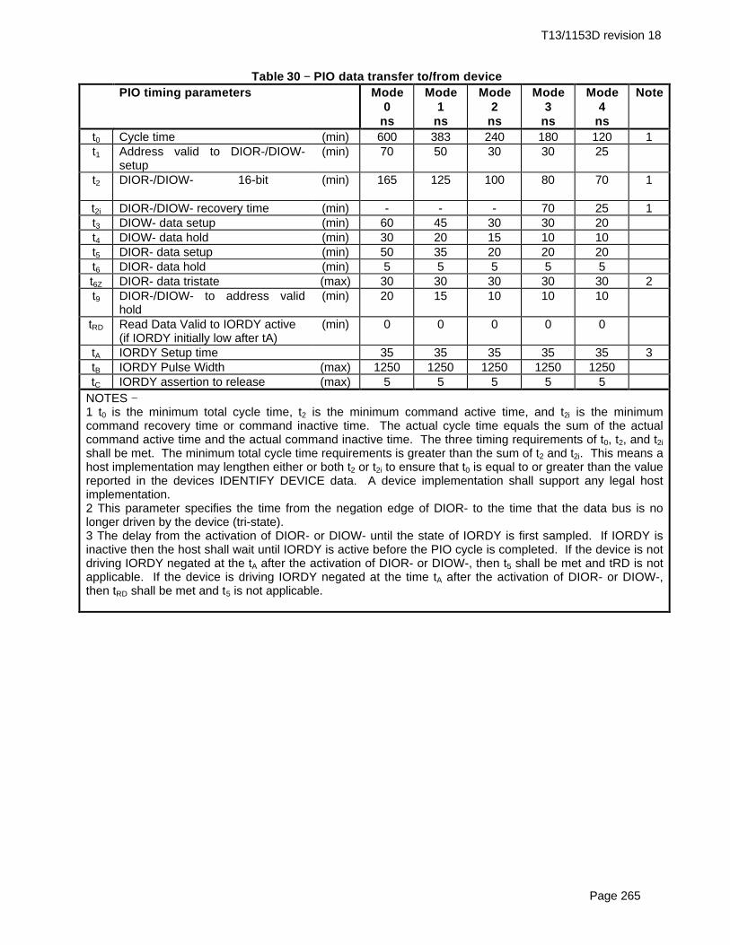
T13/1153D revision 18
Page 265
Table 30 −− PIO data transfer to/from devicePIO timing parameters Mode
0ns
Mode1
ns
Mode2
ns
Mode3
ns
Mode4
ns
Note
t0 Cycle time (min) 600 383 240 180 120 1t1 Address valid to DIOR-/DIOW-
setup(min) 70 50 30 30 25
t2 DIOR-/DIOW- 16-bit (min) 165 125 100 80 70 1
t2i DIOR-/DIOW- recovery time (min) - - - 70 25 1t3 DIOW- data setup (min) 60 45 30 30 20t4 DIOW- data hold (min) 30 20 15 10 10t5 DIOR- data setup (min) 50 35 20 20 20t6 DIOR- data hold (min) 5 5 5 5 5t6Z DIOR- data tristate (max) 30 30 30 30 30 2t9 DIOR-/DIOW- to address valid
hold(min) 20 15 10 10 10
tRD Read Data Valid to IORDY active(if IORDY initially low after tA)
(min) 0 0 0 0 0
tA IORDY Setup time 35 35 35 35 35 3tB IORDY Pulse Width (max) 1250 1250 1250 1250 1250tC IORDY assertion to release (max) 5 5 5 5 5
NOTES −1 t0 is the minimum total cycle time, t2 is the minimum command active time, and t2i is the minimumcommand recovery time or command inactive time. The actual cycle time equals the sum of the actualcommand active time and the actual command inactive time. The three timing requirements of t0, t2, and t2ishall be met. The minimum total cycle time requirements is greater than the sum of t2 and t2i. This means ahost implementation may lengthen either or both t2 or t2i to ensure that t0 is equal to or greater than the valuereported in the devices IDENTIFY DEVICE data. A device implementation shall support any legal hostimplementation.2 This parameter specifies the time from the negation edge of DIOR- to the time that the data bus is nolonger driven by the device (tri-state).3 The delay from the activation of DIOR- or DIOW- until the state of IORDY is first sampled. If IORDY isinactive then the host shall wait until IORDY is active before the PIO cycle is completed. If the device is notdriving IORDY negated at the tA after the activation of DIOR- or DIOW-, then t5 shall be met and tRD is notapplicable. If the device is driving IORDY negated at the time tA after the activation of DIOR- or DIOW-,then tRD shall be met and t5 is not applicable.

T13/1153D revision 18
Page 266
10.2.3 Multiword DMA data transfer
Figure 22 defines the timings associated with Multiword DMA transfers.
For Multiword DMA modes 1 and above, the minimum value of t0 is specified by word 65 in the IDENTIFYDEVICE parameter list. Table 31 defines the minimum value that shall be placed in word 65.
Devices shall power up with mode 0 as the default Multiword DMA mode.
CS0-/CS1- tM tN
t0
DMARQ (See note 1) tL
DMACK- (See note 2) tI tD tK tJ
DIOR-/DIOW-
tE tZ Read DD(15:0)
tG tF Write DD(15:0)
tG tH
NOTE − 1 For Multi-Word DMA transfers, the Device may negate DMARQ within the tL specified time once DMACK- is asserted and reassert it again at a later time to resume the DMA operation. Alternatively, if the device is able to continue the transfer of data, the device may leave DMARQ asserted and wait for the host to reassert DMACK-. 2 This signal may be negated by the Host to suspend the DMA transfer in process.
Figure 22 −− Multiword DMA data transfer

T13/1153D revision 18
Page 267
Table 31 −− Multiword DMA data transferMultiword DMA timingparameters
Mode 0 ns
Mode 1ns
Mode 2ns
Note
t0 Cycle time (min) 480 150 120 see notetD DIOR-/DIOW- (min) 215 80 70 see notetE DIOR- data access (max) 150 60 50tF DIOR- data hold (min) 5 5 5tG DIOR-/DIOW- data setup (min) 100 30 20tH DIOW- data hold (min) 20 15 10tI DMACK to DIOR-/DIOW- setup (min) 0 0 0tJ DIOR-/DIOW- to DMACK hold (min) 20 5 5
tKR DIOR- negated pulse width (min) 50 50 25 see notetKW DIOW- negated pulse width (min) 215 50 25 see notetLR DIOR- to DMARQ delay (max) 120 40 35tLW DIOW- to DMARQ delay (max) 40 40 35tM CS(1:0) valid to DIOR-/DIOW- (min) 50 30 25tN CS(1:0) hold (min) 15 10 10tZ DMACK- to tristate (max) 20 25 25
NOTE − t0 is the minimum total cycle time, tD is the minimum command active time, and tK (tKR or tKW, asappropriate) is the minimum command recovery time or command inactive time. The actual cycle timeequals the sum of the actual command active time and the actual command inactive time. The three timingrequirements of t0, tD, tK shall be met. The minimum total cycle time requirement, t0, is greater than the sumof tD and tK. This means a host implementation may lengthen either or both tD or tK to ensure that t0 is equalto the value reported in the devices IDENTIFY DEVICE data. A device implementation shall support anylegal host implementation.

T13/1153D revision 18
Page 268
10.2.4 Ultra DMA data transfer
Figures 23 through 32 define the timings associated with all phases of Ultra DMA bursts.
Table 32 contains the values for the timings for each of the Ultra DMA modes.
10.2.4.1 Initiating an Ultra DMA data in burst
The values for the timings for each of the Ultra DMA modes are contained in 10.2.4.2.
DMARQ(device)
DMACK-(host)
STOP(host)
HDMARDY-(host)
DSTROBE(device)
DD(15:0)
tZAD
DA0, DA1, DA2,CS0-, CS1-
tUI
tZAD
tACK
tACK
tENV
tENV
tZIORDY
tFS
tFS
tDVStAZ tDVH
tACK
NOTES −1 See 9.13.1 Initiating an Ultra DMA data in burst.2 The definitions for the STOP, HDMARDY and DSTROBE signal lines are not in effect until DMARQ and DMACK are asserted.
Figure 23 −− Initiating an Ultra DMA data in burst

T13/1153D revision 18
Page 269
10.2.4.2 Ultra DMA data burst timing requirements
Table 32 −− Ultra DMA data burst timing requirementsNAME MODE 0
(in ns)MODE 1(in ns)
MODE 2(in ns)
COMMENT
MIN MAX MIN MAX MIN MAXt2CYC 240 160 120 Typical sustained average two cycle timetCYC 114 75 55 Cycle time allowing for assymetry and clock
variations (from STROBE edge to STROBE edge)t2CYC 235 156 117 Two cycle time allowing for clock variations (from
rising edge to next rising edge or from falling edge tonext falling edge of STROBE)
tDS 15 10 7 Data setup time (at recipient)tDH 5 5 5 Data hold time (at recipient)tDVS 70 48 34 Data valid setup time at sender (from data bus being
valid until STROBE edge)tDVH 6 6 6 Data valid hold time at sender (from STROBE edge
until data may become invalid)tFS 0 230 0 200 0 170 First STROBE time (for device to first negate
DSTROBE from STOP during a data in burst)tLI 0 150 0 150 0 150 Limited interlock time (see note 1)tMLI 20 20 20 Interlock time with minimum (see note 1)tUI 0 0 0 Unlimited interlock time (see note 1)tAZ 10 10 10 Maximum time allowed for output drivers to release
(from being asserted or negated)tZAH 20 20 20 Minimum delay time required for output drivers to
assert or negate (from released state)tZAD 0 0 0tENV 20 70 20 70 20 70 Envelope time (from DMACK- to STOP and
HDMARDY- during data out burst initiation)tSR 50 30 20 STROBE to DMARDY time ( if DMARDY- is negated
before this long after STROBE edge, the recipientshall receive no more than one additional data word)
tRFS 75 60 50 Ready-to-final-STROBE time (no STROBE edgesshall be sent this long after negation of DMARDY-)
tRP 160 125 100 Ready-to-pause time (time that recipient shall wait toinitiate pause after negating DMARDY-)
tIORDYZ 20 20 20 Pull-up time before allowing IORDY to be releasedtZIORDY 0 0 0 Minimum time device shall wait before driving
IORDYtACK 20 20 20 Setup and hold times for DMACK- (before assertion
or negation)tSS 50 50 50 Time from STROBE edge to negation of DMARQ or
assertion of STOP (when sender terminates a burst)NOTES −1 tUI , tMLI , and tLI indicate sender-to-recipient or recipient-to-sender interlocks, that is, one agent (eithersender or recipient) is waiting for the other agent to respond with a signal before proceeding. tUI is anunlimited interlock that has no maximum time value. tMLI is a limited time-out that has a defined minimum.tLI is a limited time-out, that has a defined maximum.2 All timing parameters are measured at the connector of the device to which the parameter applies. Forexample, the sender shall stop generating STROBE edges tRFS after the negation of DMARDY-. BothSTROBE and DMARDY- timing measurements are taken at the connector of the sender. Even though thesender stops generating STROBE edges, additional STROBE edges may be received by the receiver dueto propagation delay (see 9.13.3.2).3 All timing measurement switching points (low to high and high to low) are to be taken at 1.5V.

T13/1153D revision 18
Page 270
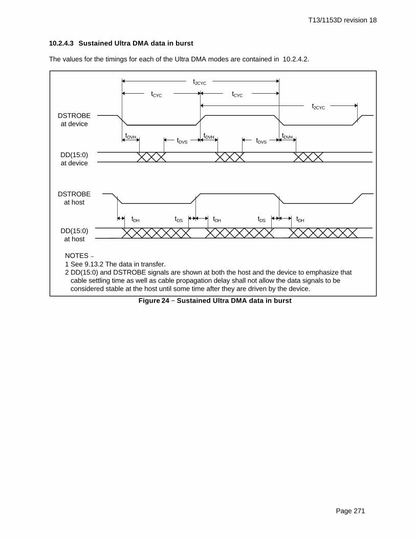
T13/1153D revision 18
Page 271
10.2.4.3 Sustained Ultra DMA data in burst
The values for the timings for each of the Ultra DMA modes are contained in 10.2.4.2.
tDVH
DSTROBEat device
DD(15:0)at device
DSTROBEat host
DD(15:0)at host
tDVH
tCYC tCYC
tDVS tDVS
tDH tDS tDH tDS
t2CYC
tDH
tDVH
t2CYC
NOTES −1 See 9.13.2 The data in transfer.2 DD(15:0) and DSTROBE signals are shown at both the host and the device to emphasize that cable settling time as well as cable propagation delay shall not allow the data signals to be considered stable at the host until some time after they are driven by the device.
Figure 24 −− Sustained Ultra DMA data in burst

T13/1153D revision 18
Page 272
10.2.4.4 Host pausing an Ultra DMA data in burst
The values for the timings for each of the Ultra DMA modes are contained in 10.2.4.2.
DMARQ(device)
DMACK-(host)
STOP(host)
HDMARDY-(host)
DSTROBE(device)
DD(15:0)(device)
tSR
tRFS
tRP
−
Figure 25 −− Host pausing an Ultra DMA data in burst

T13/1153D revision 18
Page 273
10.2.4.5 Device terminating an Ultra DMA data in burst
The values for the timings for each of the Ultra DMA modes are contained in 10.2.4.2.
tAZ
tIORDYZ
CRC
DMARQ(device)
DMACK-(host)
STOP(host)
HDMARDY-(host)
DSTROBE(device)
DD(15:0)
DA0, DA1, DA2,CS0-, CS1-
tACK
tLI
tMLI
tDVS
tLI
tACK
tACK
tZAH
tDVH
tSS
tLI
NOTES −1 See 9.13.4.1 Device terminating an Ultra DMA data in burst.2 The definitions for the STOP, HDMARDY and DSTROBE signal lines are no longer in effect after DMARQ and DMACK are negated.
Figure 26 −− Device terminating an Ultra DMA data in burst
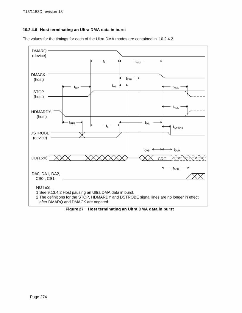
T13/1153D revision 18
Page 274
10.2.4.6 Host terminating an Ultra DMA data in burst
The values for the timings for each of the Ultra DMA modes are contained in 10.2.4.2.
tDVH
CRC
tAZ
DMARQ(device)
DMACK-(host)
STOP(host)
HDMARDY-(host)
DSTROBE(device)
DD(15:0)
DA0, DA1, DA2,CS0-, CS1-
tACK
tMLItLI
tLI tIORDYZ
tACK
tACK
tZAH
tMLI
tDVS
tRFS
tRP
NOTES −1 See 9.13.4.2 Host pausing an Ultra DMA data in burst.2 The definitions for the STOP, HDMARDY and DSTROBE signal lines are no longer in effect after DMARQ and DMACK are negated.
Figure 27 −− Host terminating an Ultra DMA data in burst

T13/1153D revision 18
Page 275
10.2.4.7 Initiating an Ultra DMA data out burst
The values for the timings for each of the Ultra DMA modes are contained in 10.2.4.2.
DMARQ(device)
DMACK-(host)
STOP(host)
DDMARDY-(device)
HSTROBE(host)
DD(15:0)(host)
DA0, DA1, DA2,CS0-, CS1-
tUI
tACK tENV
tZIORDY tLI
tDVS tDVH
tACK
tACK
tUI
NOTES −1 See 9.14.1 Initiating an Ultra DMA data out burst.2 The definitions for the STOP, DDMARDY and HSTROBE signal lines are not in effect until DMARQ and DMACK are asserted.
Figure 28 −− Initiating an Ultra DMA data out burst
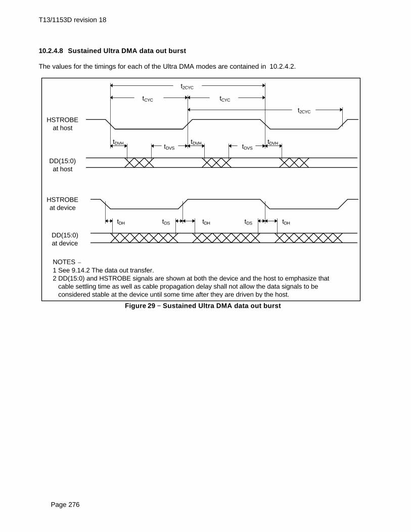
T13/1153D revision 18
Page 276
10.2.4.8 Sustained Ultra DMA data out burst
The values for the timings for each of the Ultra DMA modes are contained in 10.2.4.2.
tDH tDS
tDVH
HSTROBEat host
DD(15:0)at host
HSTROBEat device
DD(15:0)at device
tDVH
tCYC tCYC
tDVS tDVS
tDS tDH
t2CYC
tDH
tDVH
t2CYC
NOTES −1 See 9.14.2 The data out transfer.2 DD(15:0) and HSTROBE signals are shown at both the device and the host to emphasize that cable settling time as well as cable propagation delay shall not allow the data signals to be considered stable at the device until some time after they are driven by the host.
Figure 29 −− Sustained Ultra DMA data out burst

T13/1153D revision 18
Page 277
10.2.4.9 Device pausing an Ultra DMA data out burst
The values for the timings for each of the Ultra DMA modes are contained in 10.2.4.2.
DMARQ(device)
DMACK-(host)
STOP(host)
DDMARDY-(device)
HSTROBE(host)
DD(15:0)(host)
tSR
tRFS
tRP
NOTES − 1 See 9.14.3.2 Device pausing an Ultra DMA data out burst. 2 The device may negate DMARQ to request termination of the Ultra DMA burst no sooner than tRP after DDMARDY- is negated. 3 If the tSR timing is not statisfied, the device may receive zero, one, or two more data words from the host.
Figure 30 −− Device pausing an Ultra DMA data out burst

T13/1153D revision 18
Page 278
10.2.4.10 Host terminating an Ultra DMA data out burst
The values for the timings for each of the Ultra DMA modes are contained in 10.2.4.2.
DMARQ(device)
DMACK-(host)
STOP(host)
DDMARDY-(device)
HSTROBE(host)
DD(15:0)(host)
DA0, DA1, DA2,CS0-, CS1-
tACK
tLI
tMLI
tDVS
tLI
tLI
tACK
tIORDYZ
tACK
CRC
tDVH
tSS
NOTES −1 See 9.14.4.1 Host terminating an Ultra DMA data out burst.2 The definitions for the STOP, DDMARDY and HSTROBE signal lines are no longer in effect after DMARQ and DMACK are negated.
Figure 31 −− Host terminating an Ultra DMA data out burst

T13/1153D revision 18
Page 279
10.2.4.11 Device terminating an Ultra DMA data out burst
The values for the timings for each of the Ultra DMA modes are contained in 10.2.4.2.
DMARQ(device)
DMACK-(host)
STOP(host)
DDMARDY-(device)
HSTROBE(host)
DD(15:0)(host)
DA0, DA1, DA2,CS0-, CS1-
tACK
tMLI
tDVS
tLI
tLI
tACK
CRC
tDVH
tACK
tIORDYZ
tMLI
tRP
tRFS
NOTES −1 See 9.14.4.2 Device pausing an Ultra DMA data out burst.2 The definitions for the STOP, DDMARDY and HSTROBE signal lines are no longer in effect after DMARQ and DMACK are negated.
Figure 32 −− Device terminating an Ultra DMA data out burst

T13/1153D revision 18
Page 280
Annex A(normative)
Connectors
The device shall implement one of the connector options described in this annex.
A.1 40-pin connector
The I/O connector is a 40-pin connector as described by SFF8059. The connector is as shown in figure A.1with pin assignments as shown in table A.1. The connector shall be keyed to prevent the possibility ofinstalling it upside down. A key is provided by the removal of pin 20. The corresponding pin on the cableconnector shall be plugged.
The pin locations are governed by the cable plug, not the receptacle. The way in which the receptacle ismounted on the printed circuit board affects the pin positions, and pin 1 shall remain in the same relativeposition. This means the pin numbers of the receptacle may not reflect the conductor number of the plug.The header receptacle is not polarized, and all the signals are relative to pin 20, that is keyed.
By using the plug positions as primary, a straight cable connects devices. As shown in figure A.2, conductor1 on pin 1 of the plug shall be in the same relative position no matter what the receptacle numbering lookslike. If receptacle numbering was followed, the cable would have to twist 180 degrees between a devicewith top-mounted receptacles, and a device with bottom-mounted receptacles.
39
19 1
K40
20
2
Not to scaleFigure A.1 −− 40-pin connector
140 20 2
Circuit board Circuit board1
40 20 2
Not to scaleFigure A.2 −− 40-pin connector mounting
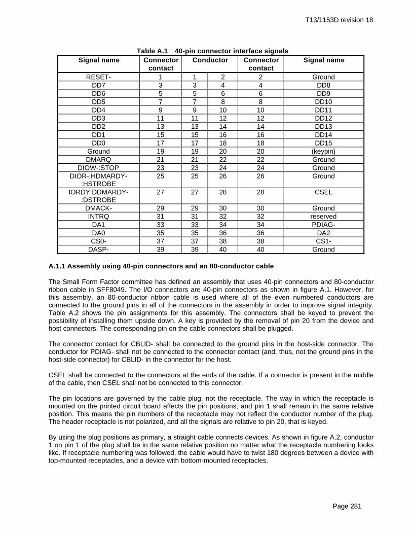
T13/1153D revision 18
Page 281
Table A.1 −− 40-pin connector interface signalsSignal name Connector
contactConductor Connector
contactSignal name
RESET- 1 1 2 2 GroundDD7 3 3 4 4 DD8DD6 5 5 6 6 DD9DD5 7 7 8 8 DD10DD4 9 9 10 10 DD11DD3 11 11 12 12 DD12DD2 13 13 14 14 DD13DD1 15 15 16 16 DD14DD0 17 17 18 18 DD15
Ground 19 19 20 20 (keypin)DMARQ 21 21 22 22 Ground
DIOW-:STOP 23 23 24 24 GroundDIOR-:HDMARDY-
:HSTROBE25 25 26 26 Ground
IORDY:DDMARDY-:DSTROBE
27 27 28 28 CSEL
DMACK- 29 29 30 30 GroundINTRQ 31 31 32 32 reserved
DA1 33 33 34 34 PDIAG-DA0 35 35 36 36 DA2CS0- 37 37 38 38 CS1-
DASP- 39 39 40 40 Ground
A.1.1 Assembly using 40-pin connectors and an 80-conductor cable
The Small Form Factor committee has defined an assembly that uses 40-pin connectors and 80-conductorribbon cable in SFF8049. The I/O connectors are 40-pin connectors as shown in figure A.1. However, forthis assembly, an 80-conductor ribbon cable is used where all of the even numbered conductors areconnected to the ground pins in all of the connectors in the assembly in order to improve signal integrity.Table A.2 shows the pin assignments for this assembly. The connectors shall be keyed to prevent thepossibility of installing them upside down. A key is provided by the removal of pin 20 from the device andhost connectors. The corresponding pin on the cable connectors shall be plugged.
The connector contact for CBLID- shall be connected to the ground pins in the host-side connector. Theconductor for PDIAG- shall not be connected to the connector contact (and, thus, not the ground pins in thehost-side connector) for CBLID- in the connector for the host.
CSEL shall be connected to the connectors at the ends of the cable. If a connector is present in the middleof the cable, then CSEL shall not be connected to this connector.
The pin locations are governed by the cable plug, not the receptacle. The way in which the receptacle ismounted on the printed circuit board affects the pin positions, and pin 1 shall remain in the same relativeposition. This means the pin numbers of the receptacle may not reflect the conductor number of the plug.The header receptacle is not polarized, and all the signals are relative to pin 20, that is keyed.
By using the plug positions as primary, a straight cable connects devices. As shown in figure A.2, conductor1 on pin 1 of the plug shall be in the same relative position no matter what the receptacle numbering lookslike. If receptacle numbering was followed, the cable would have to twist 180 degrees between a device withtop-mounted receptacles, and a device with bottom-mounted receptacles.
T13/1153D revision 18
Page 282
Table A.2 −− 40-pin connector interface signals using 80-conductor cableSignal name Connecto
r contactConductor Connector
contactSignal name
RESET- 1 1 3 2 GroundDD7 3 5 7 4 DD8DD6 5 9 11 6 DD9DD5 7 13 15 8 DD10DD4 9 17 19 10 DD11DD3 11 21 23 12 DD12DD2 13 25 27 14 DD13DD1 15 29 31 16 DD14DD0 17 33 35 18 DD15
Ground 19 37 39 20 (keypin)DMARQ 21 41 43 22 Ground
DIOW-:STOP 23 45 47 24 GroundDIOR-:HDMARDY-
:HSTROBE25 49 51 26 Ground
IORDY:DDMARDY-:DSTROBE
27 53 55 28 CSEL (see note 2)
DMACK- 29 57 59 30 GroundINTRQ 31 61 63 32 reserved
DA1 33 65 67 34 PDIAG-:CBLID-(see note3)
DA0 35 69 71 36 DA2CS0- 37 73 75 38 CS1-
DASP- 39 77 79 40 GroundNOTES −1 All even-numbered conductors are connected to ground inside each of the connectors.2 In a cable assembly providing connectors for two devices and a host, conductor 55 shall not beconnected to connector contact 28 in the connector in the middle position. This configurationresults in Device 0 being at the opposite end of the cable from the host.3 Connector contact 34 in the connector for the host shall be connected to the ground pins in thehost-side connector. Conductor 67 shall not be connected to connector contact 34 in the connectorfor the host.
A.1.2 4-pin power connector
When the device uses the 40-pin connector, the device receives DC power through a 4-pin connector asdefined by SFF8012. The pin assignments are shown in table A.2.
Table A.2 −− DC interface using 4-pin power connectorPower line designation Pin Number
+12 Volts 1+12 Volt return 2+5 Volt return 3
+5 Volts 4
4 3 2 1 +5 V DC +5 V return +12 V return +12 V DC
Not to scaleFigure A.3 −− Device side connector pin numbering
T13/1153D revision 18
Page 283
A.2 44-pin small form factor connector
This annex describes a connector alternative often used for 2 1/2 inch or smaller devices. This alternativeis defined by the SFF8212.
A.2.1 44-pin signal assignments
The signals assigned for 44-pin applications are described in table A.3. Although there are 50 pins in theplug, a 44-pin mating receptacle may be used (the removal of pins E and F provides room for the wall of thereceptacle).
Some devices may utilize pins A, B, C, and D for option selection via physical jumpers. Suchimplementations may require use of the 44-pin receptacle.
Pins A through D of the connector plug located on the device shall not be connected to the host, as they arereserved for manufacturer's use. Pins E, F, and 20 are keys, and are removed (see figure A.4).
43
19 1 E C A
KK K
44
20
2 F D B
Not to scaleFigure A.4 −− 44-pin connector
A.2.2 Use of pins A-D for device selection
If a device uses pins A, B, C, and D for device selection, when no jumper is present the device should bedesignated as Device 0. When a jumper is present between pins B and D, the device should to respond tothe CSEL signal to determine its device number.

T13/1153D revision 18
Page 284
Table A.3 −− Signal assignments for 44-pin connectorSignal name Connector
contactConductor Connector
contactSignal name
Vendor specific (see note) A B Vendor specific (see note)Vendor specific (see note) C D Vendor specific (see note)
(keypin) (see note) E F (keypin) (see note)RESET- 1 1 2 2 Ground
DD7 3 3 4 4 DD8DD6 5 5 6 6 DD9DD5 7 7 8 8 DD10DD4 9 9 10 10 DD11DD3 11 11 12 12 DD12DD2 13 13 14 14 DD13DD1 15 15 16 16 DD14DD0 17 17 18 18 DD15
Ground 19 19 20 20 (keypin)DMARQ 21 21 22 22 Ground
DIOW-:STOP 23 23 24 24 GroundDIOR-:HDMARDY-
:HSTROBE25 25 26 26 Ground
IORDY:DDMARDY-:DSTROBE
27 27 28 28 CSEL
DMACK- 29 29 30 30 GroundINTRQ 31 31 32 32 reserved
DA1 33 33 34 34 PDIAG-DA0 35 35 36 36 DA2CS0- 37 37 38 38 CS1-
DASP- 39 39 40 40 Ground+5 V (logic)(see note)
41 41 42 42 +5 V (Motor)(see note)
Ground(return)(see note)
43 43 44 44 Reserved - no connection(see note)
NOTE − Pins that are additional to those of the 40-pin cable.

T13/1153D revision 18
Page 285
A.3 68-pin small form factor connector
This clause defines the pinouts used for the 68-pin alternative connector for the AT Attachment Interface.This connector is defined in the PCMCIA PC Card Standard. This clause defines a pinout alternative thatallows a device to function as an AT Attachment Interface compliant device, while also allowing the deviceto be compliant with PC Card ATA mode defined by PCMCIA. The signal protocol allows the device toidentify the host interface as being 68-pin as defined in this standard or PC Card ATA.
To simplify the implementation of dual-interface devices, the 68-pin AT Attachment Interface maintainscommonality with as many PC Card ATA signals as possible, while supporting full command and signalcompliance with this standard.
The 68-pin pinout shall not cause damage or loss of data if a PCMCIA card is accidentally plugged into ahost slot supporting this interface. The inversion of the RESET signal between this standard and PCMCIAinterfaces prevents loss of data if the device is unable to reconfigure itself to the appropriate host interface.
A.3.1 Signals
This specification relies upon the electrical and mechanical characteristics of PCMCIA and unless otherwisenoted, all signals and registers with the same names as PCMCIA signals and registers have the samemeaning as defined in PCMCIA.
The PC Card-ATA specification is used as a reference to identify the signal protocol used to identify the hostinterface protocol.
A.3.2 Signal descriptions
Any signals not defined below shall be as described in this standard, PCMCIA, or the PC Card ATAdocuments.
Table A.4 shows the signals and relationships such as direction, as well as providing the signal name of thePCMCIA equivalent.

T13/1153D revision 18
Page 286
Table A.4 −− Signal assignments for 68-pin connectorPin Signal Hst Dir Dev PCMCIA Pin Signal Hst Dir Dev PCMCIA1 Ground x → x Ground 35 Ground x → x Ground2 DD3 x ↔ x D3 36 CD1- x ← x CD1-3 DD4 x ↔ x D4 37 DD11 x ↔ x D114 DD5 x ↔ x D5 38 DD12 x ↔ x D125 DD6 x ↔ x D6 39 DD13 x ↔ x D136 DD7 x ↔ x D7 40 DD14 x ↔ x D147 CS0- x → x CE1- 41 DD15 x ↔ x D158 → i A10 42 CS1- x → x(1) CE2-9 SELATA- x → x OE- 43 ← i VS1-
10 44 DIOR- x → x IORD-11 CS1- x → x(1) A9 45 DIOW- x → x IOWR-12 → i A8 4613 4714 4815 → i WE- 4916 INTRQ x ← x READY/
IREQ-50
17 Vcc x → x Vcc 51 Vcc x → x Vcc18 5219 5320 5421 55 M/S- x → x(2)22 → i A7 56 CSEL x → x(2)23 → i A6 57 ← i VS2-24 → i A5 58 RESET- x → x RESET25 → i A4 59 IORDY o ← x(3) WAIT-26 → i A3 60 DMARQ o ← x(3) INPACK-27 DA2 x → x A2 61 DMACK- o → o REG-28 DA1 x → x A1 62 DASP- x ↔ x BVD2/
SPKR-29 DA0 x → x A0 63 PDIAG- x ↔ x BVD1/
STSCHG30 DD0 x ↔ x D0 64 DD8 x ↔ x D831 DD1 x ↔ x D1 65 DD9 x ↔ x D932 DD2 x ↔ x D2 66 DD10 x ↔ x D1033 x ← x WP/
IOIS1667 CD2- x ← x CD2-
34 Ground x → x Ground 68 Ground x → x GroundKey:Dir = the direction of the signal between host and device.x in the Hst column = this signal shall be supported by the Host.x in the Dev column = this signal shall be supported by the device.i in the Dev column = this signal shall be ignored by the device while in 68-pin mode as defined in thisstandard.o = this signal is Optional.Nothing in Dev column = no connection should be made to that pin.
NOTES −1 The device shall support only one CS1- signal pin.2 The device shall support either M/S- or CSEL but not both.3 The device shall hold this signal negated if it does not support the function.
T13/1153D revision 18
Page 287
A.3.2.1 CD1- (Card Detect 1)
This signal shall be grounded by the device. CD1- and CD2- are used by the host to detect the presence ofthe device.
A.3.2.2 CD2- (Card Detect 2)
This signal shall be grounded by the device. CD1- and CD2- are used by the host to detect the presence ofthe device.
A.3.2.3 CS1- (Device chip select 1)
Hosts shall provide CS1- on both the pins identified in table A.4.
Devices shall recognize only one of the two pins as CS1-.
A.3.2.4 DMACK- (DMA acknowledge)
This signal is optional for hosts and devices.
If this signal is supported by the host or the device, the function of DMARQ shall also be supported.
A.3.2.5 DMARQ (DMA request)
This signal is optional for hosts.
If this signal is supported by the host or the device, the function of DMACK- shall also be supported.
A.3.2.6 IORDY (I/O channel ready)
This signal is optional for hosts.
A.3.2.7 M/S- (Master/slave)
This signal is the inverted form of CSEL. Hosts shall support both M/S- and CSEL though devices need onlysupport one or the other.
Hosts shall assert CSEL and M/S- prior to applying VCC to the connector.
A.3.2.8 SELATA- (Select 68-pin ATA)
This pin is used by the host to select which mode to use, PC Card-ATA mode or the 68-pin mode defined inthis standard. To select 68-pin ATA mode, the host shall assert SELATA- prior to applying power to theconnector, and shall hold SELATA- asserted.
The device shall not re-sample SELATA- as a result of either a hardware or software reset. The device shallignore all interface signals for 19 ms after the host supplies Vcc within the device's voltage tolerance. IfSELATA- is negated following this time, the device shall either configure itself for PC Card-ATA mode or notrespond to further inputs from the host.
A.3.3 Removability considerations
This specification supports the removability of devices that use the protocol. As removability is a newconsideration for devices, several issues need to be considered with regard to the insertion or removal ofdevices.

T13/1153D revision 18
Page 288
A.3.3.1 Device recommendations
The following are recommendations to device implementors:
− CS0-, CS1-, RESET-, and SELATA- signals be negated on the device to prevent false selectionduring hot insertion.
− Ignore all interface signals except SELATA- until 19 ms after the host supplies VCC within the
device's voltage tolerance. This time is necessary to de-bounce the device's power on resetsequence. Once in the 68-pin mode as defined in this standard, if SELATA- is ever negatedfollowing the 19 ms de-bounce delay time, the device disables itself until VCC is removed.
− The DOOR LOCK and DOOR UNLOCK commands and the MC and MCR bits in the Error
register are used to prevent unexpected removal of the device or media.
A.3.3.2 Host recommendations
The following are recommendations to host implementors:
− Connector pin sequencing to protect the device by making contact to ground before any othersignal in the system.
− SELATA- to be asserted at all times. − All devices reset and reconfigured to the same base address each time a device at that address
is inserted or removed. − The removal or insertion of a device at the same address to be detected so as to prevent the
corruption of a command. − The DOOR LOCK and DOOR UNLOCK commands and the MC and MCR bits in the Error
register used to prevent unexpected removal of the device or media.
A.4 Unitized connectors
The Small Form Factor committee has defined two unitized connectors for use on ATA/ATAPI devices of3.5” and larger form factor. Each of these connectors consists of a signal portion that complies with the 40-pin signal definition of A.1 and a 4-pin power portion that complies with the definition in A.1.1. In addition,each has a jumper connector portion.
Figure A.5 shows the unitized connector defined by SFF8057 and defines the usage of the jumper connectorpins.
Figure A.6 shows the unitized connector defined by SFF8058 and defines the usage of the jumper connectorpins.
T13/1153D revision 18
Page 289
40-pin signal connector 4-pin power connector Pin 1 Pin A
Pin 40 Pin H Jumper connector
Jumpers: E-F - CSEL No jumper - Slave G-H - Master G-H and E-F - Master w/Slave present Use of pins A through D is vendor specific Pin I is reserved Not to scale
Figure A.5 −− SFF 8057 connector
40-pin signal connector 4-pin power connector Pin 1 Pin A
Pin 40 Pin J Jumper connector
Jumpers: A-B - CSEL C-D - Slave E-F - Master Use of pins G through J is vendor specific
Not to scale
Figure A.6 −− SFF 8058 connector

T13/1153D revision 18
Page 290
Annex B
(informative)Identify device data for devices with more than 1024 logical cylinders
B.1 Definitions and background information
The original IBM PC BIOS (Basic Input/Output System) imposed several restrictions on the support ofdevices, and these have been incorporated into many higher level software products. One such restrictionlimits the capacity of a device. BIOS software cannot support a device with more than 1,024 cylinders, 16heads, and 63 sectors per track without translating an input logical geometry to a different output logicalgeometry. The maximum addressable capacity of a device that does not require BIOS translation is1,032,192 sectors.
These rules allow BIOSes using bit shifting translation to access 15,481,935 (16,383*15*63) sectors, andBIOSes using LBA assisted translation to access 16,450,560 (1024*255*63) sectors. Extended BIOSfunctionality is defined in the ANSI Technical Report Enhanced BIOS Services for Disk Drives, whichdescribes new services provided by BIOS firmware to support ATA hard disks up to 16 mega-terra-sectors.
B.2 Cylinder, head, and sector addressing
BIOSs and other software that operate a device in CHS translation employ a combination of IDENTIFYDEVICE data words 1, 3, 6, words 53-58, and words 60-61 to ascertain the appropriate translation to useand determine the capacity of a device.
Maximum compatibility is facilitated if the following guidelines are used. These guidelines limit the valuesplaced into words 1, 3, 6, 53-58, and 60-61. Accessing beyond 15,481,935 sectors should be performedusing LBA.
B.2.1 Word 1
For devices with a capacity less than or equal to 1,032,192 sectors, if IDENTIFY DEVICE data word 1(Default Cylinders) does not specify a value greater than 1,024, then no guideline is necessary.
If a device is greater than 1,032,192 sectors, but less than or equal to 16,514,064 sectors, the maximumvalue that can be placed into this word is determined by the value in word 3 as shown in table B.1.
If a device is greater than 15,481,935 sectors and supports CHS, this word should contain 16,383 (3FFFh).
The INITIALIZE DEVICE PARAMETERS command does not change this value.
The value in this word is changed by the SET MAX ADDRESS command.
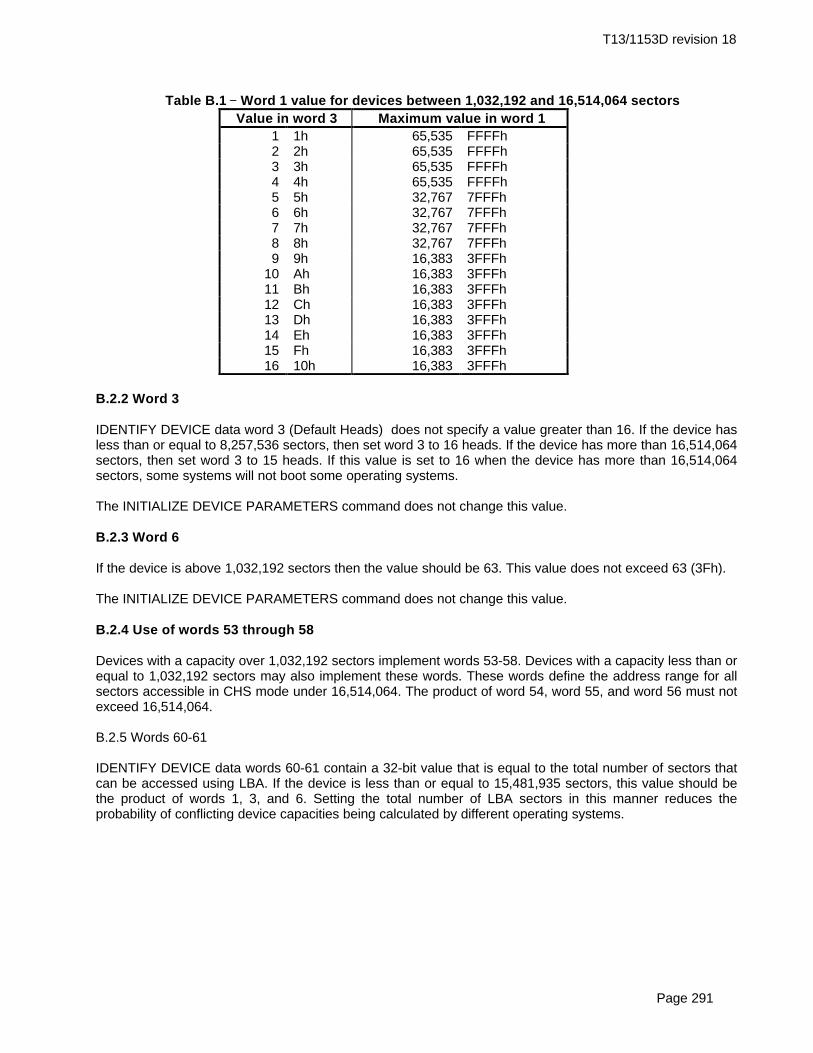
T13/1153D revision 18
Page 291
Table B.1 −− Word 1 value for devices between 1,032,192 and 16,514,064 sectorsValue in word 3 Maximum value in word 1
1 1h 65,535 FFFFh2 2h 65,535 FFFFh3 3h 65,535 FFFFh4 4h 65,535 FFFFh5 5h 32,767 7FFFh6 6h 32,767 7FFFh7 7h 32,767 7FFFh8 8h 32,767 7FFFh9 9h 16,383 3FFFh
10 Ah 16,383 3FFFh11 Bh 16,383 3FFFh12 Ch 16,383 3FFFh13 Dh 16,383 3FFFh14 Eh 16,383 3FFFh15 Fh 16,383 3FFFh16 10h 16,383 3FFFh
B.2.2 Word 3
IDENTIFY DEVICE data word 3 (Default Heads) does not specify a value greater than 16. If the device hasless than or equal to 8,257,536 sectors, then set word 3 to 16 heads. If the device has more than 16,514,064sectors, then set word 3 to 15 heads. If this value is set to 16 when the device has more than 16,514,064sectors, some systems will not boot some operating systems.
The INITIALIZE DEVICE PARAMETERS command does not change this value.
B.2.3 Word 6
If the device is above 1,032,192 sectors then the value should be 63. This value does not exceed 63 (3Fh).
The INITIALIZE DEVICE PARAMETERS command does not change this value.
B.2.4 Use of words 53 through 58
Devices with a capacity over 1,032,192 sectors implement words 53-58. Devices with a capacity less than orequal to 1,032,192 sectors may also implement these words. These words define the address range for allsectors accessible in CHS mode under 16,514,064. The product of word 54, word 55, and word 56 must notexceed 16,514,064.
B.2.5 Words 60-61
IDENTIFY DEVICE data words 60-61 contain a 32-bit value that is equal to the total number of sectors thatcan be accessed using LBA. If the device is less than or equal to 15,481,935 sectors, this value should bethe product of words 1, 3, and 6. Setting the total number of LBA sectors in this manner reduces theprobability of conflicting device capacities being calculated by different operating systems.

T13/1153D revision 18
Page 292
B.3 Orphan sectors
The sectors, if any, between the last sector addressable in CHS mode and the last sector addressable inLBA mode are known as "orphan" sectors. A device may or may not allow access to these sectors in CHSaddressing mode.
The values in words 1, 3, and 6 are selected such that the number of orphan sectors is minimized.Normally, the number of orphan sectors should not exceed ( [word55] x [word56] - 1 ). However, the hostsystem may create conditions where there are a larger number of orphans sectors by issuing the INITIALIZEDEVICE PARAMETERS command with values other than the values in words 3 and 6. If therecommendation in B.2.5 is followed, there will be no orphan sectors and problems associated with newoperating systems calculating a different device size from older operating systems will be minimized.

T13/1153D revision 18
Page 293
Annex C(informative)
Signal integrity
C.1 Introduction
The ATA bus (a.k.a. IDE bus) is a disk drive interface originally designed for the ISA Bus of the IBMPC/AT. With the advent of faster devices the definition of the bus has been expanded to include newoperating modes. Each of the PIO modes, numbered zero through four, is faster than the one before it(higher numbers translate to faster transfer rates). PIO modes 0, 1, and 2 correspond to transfer rates forthe interface as it was originally defined with maximum transfer rates of 3.3, 5.2, and 8.3 MB/s, respectively.PIO mode 3 defines a maximum transfer rate of 11.1 MB/s, and PIO mode 4 defines a maximum rate of16.7 MB/s. Additionally, Multiword DMA and Ultra DMA modes have been defined. Multiword DMA mode0, 1, and 2 have maximum transfer rates of 4.2, 13.3, and 16.7 MB/s, respectively. Ultra DMA modes 0, 1,and 2 have maximum transfer rates of 16.7, 25, and 33.3 MB/s, respectively.
With the increases in speed the weaknesses of the original cabling scheme has become apparent. Systemmanufacturers, chipset designers, and device manufacturers must all take measures to insure that signalintegrity is maintained on the bus. The areas of concern are:
a) ringing due to improper termination;b) crosstalk between signals;c) bus timing.
The intended audience for this annex is digital and analog engineers who design circuits interfacing to theATA bus. Familiarity with this standard and a basic understanding of circuit theory is assumed.
C.1.1 The problems
Early implementations of the bus used LS-TTL parts to drive an 18-inch cable. The slow edges of LS-TTLand the short cable length worked well at the time. PIO modes 3 and 4 demand higher performance. In aneffort to cut cycle times, edge rates have inadvertently been increased, causing ringing on the cable andincreased crosstalk between adjacent signals.
When a host adapter was little more than a few buffers and some gates there was no issue with host adaptertiming. With the advent of local bus architectures and faster transfer rates, timing issues have becomemore important. Propagation delay with worst-case loads must now be taken into account when designinghost adapters.
One of the frequently asked questions is, “Why are problems with ringing on the bus seen now when theywere not seen before?” The answer is in the edge speed of the logic. How the edge speed changed may befound by looking at the history of the IBM PC.
When the IBM PC/AT was introduced in 1983, the 8 MHz 80286 processor quickly became the dominantplatform. The AT bus (now called the ISA bus) became standardized around an 8 MHz processor speed.When the first disk drive was introduced a few years later, it was designed as a simple extension of the busleading to the name “AT Attachment” interface (see figure C.1). The idea was to remove the disk drivecontroller electronics from the PC and place them on the drive instead. What remained on the PC was apair of bi-directional data buffers and an address decoder. This simple interface was most oftenimplemented with a pair of 74LS245 buffers and a programmable logic device such as a PAL. These TTLdevices had rise and fall times in the 5 to 6 ns range. Although this was fast enough to cause some ringingon the bus, it was not so severe as to prevent millions of successful system implementations.

T13/1153D revision 18
Page 294
CPU 8 Mhz
Bus Interface
RAM
ROM
ATA Intf (simple)
Device
CardSlots
ISA Bus
8 Mhz
Figure C.1 −− Original IBM PC/AT architecture
The architecture of modern PCs has changed from the original PC/AT. As the processor speed increasedit became necessary to separate the processor bus from the ISA bus (see figure C.2). To maintaincompatibility the ISA bus continues to run at an 8 MHz rate. Processors have increased beyond 200 MHz,and their associated busses have increased from 8 MHz to 33 MHz and above.
Devices have also increased in speed. The increase in rotational speed and linear bit density has increasedthe rate at that data comes off the heads, and the presence of cache on the device makes data available atthe access rates of RAM. This has created a data bottleneck at the ISA bus. The device is faster, theprocessor is faster, but the data can’t be moved from one to the other any faster.
CPU 200 Mhz
RAM
ROM
Bus Interface
Local Bus Interface
ATA Intf (complex)
Device
ISA Bus
8 Mhz
Local Bus
33 MHZATA
(fast)
CardSlots
LocalBusCardSlots
Figure C.2 −− Modern PC architecture
This bottleneck inspired the invention of new, faster interfaces to the processor. Local busses are designedto run at the speed of the processor bus. Two local bus standards have emerged, the VESA Local Bus(VLB) and the Peripheral Component Interconnect bus (PCI). These local busses have the potential forfaster data transfer from the device to the processor.
To allow devices to transfer data faster, the standard had to be updated to allow faster transfer modes.These enhanced modes are still not as fast as a processor bus. To synchronize the data flow between 32-bit 33 MHz processor busses and slower 16-bit devices, a VLSI chip is required. Most of these bridge chips
T13/1153D revision 18
Page 295
were implemented with fast CMOS processes to achieve the required bus speeds. As a result the edgerates on the bus were often 1 to 2 ns, and sometimes less. These fast edges have aggravated the ringingon the bus to the point that system/device combinations fail to work.
In summary, the reason for signal integrity problems appearing now, when they were absent before, is theadvent of faster transfer rates on the bus coupled with a change of IC process at the interface. Theproblems are not insurmountable, and the bus can be a robust, fast, and inexpensive interface.
C.1.2 The goals
The recommendations in this annex make the following assumptions. The word “device” is used genericallyto describe hard disk drives and other peripheral devices on the bus.
− Backward compatibility must be maintained. Old devices must work with new host adapters, and oldhost adapters must work with new devices.
− This standard must be followed as closely as possible. Without this, solutions implemented by differentmanufacturers will tend to diverge, creating incompatible systems.
− Solutions must be simple and inexpensive. The market for these products is very cost sensitive.
C.2 Termination
When analyzing the bus, the standard 18-inch ribbon cable used to connect devices must be considered inthree different areas of frequency. At low frequencies it is a lumped capacitive load; higher in frequency it isa lumped LCR circuit; and at high frequencies it is a transmission line with distributed parameters. Atstandard transfer rates both the LCR circuit and distributed model apply.
The cable used in most systems is a PVC-coated 40-conductor ribbon cable with the conductor spacing at0.05 inches on center. This cable is modeled as a transmission line with a typical characteristic impedanceof 110 ohms and propagation velocity of 60% c when connected in a ground-signal-ground configuration.When there are fewer grounds the characteristic impedance is higher. For the data lines adjacent to groundlines the characteristic impedance is about 160 ohms. The 110 ohm case applies to data strobes.
C.2.1 The problem
Many users experienced problems with early implementations of PIO mode 3 devices and hosts. Mostfailures in the systems observed were attributed to signal integrity problems on the control lines that go fromthe host to the device. The problem appears most frequently as ringing on the DIOR- (during readcommands) and DIOW- (during write commands) lines.
During a read cycle when DIOR- is asserted, it is possible for the ringing to create a short duration negationpulse (see figure C.3). This pulse occurs early in the read cycle. Inside the interface portion of the datapath controller chip is a FIFO buffer that contains the data to be read. The extra pulse on the DIOR- lineadvances the FIFO pointer by one. This results in losing one word of data. The host system read operationtherefore receives one word too few, and the remaining bytes are shifted. A typical data word (Wn)sequence might look like . . .W7, W8, W9, W11, W12 . . . Notice that word 10 is missing from the returneddata. This also means that the host tries to read one more word from the device than the device hasremaining in its buffer. Depending on the implementation of the BIOS, this locks up the system or simplyreturns a byte of random data at the end of the sector transfer.
Pulse slivers due to ringing on the DIOW- line cause a similar problem during write transfers. The pulsesliver advances the FIFO pointer by one, writing an extra word of random data into the FIFO. Subsequentdata bytes are shifted by one word. A typical stored data word (Wn) sequence on the device might look like. . . W7, W8, W9, XX, W10, W11 . . . In this example an extra word was inserted during the write cycle forword 10. From the device's point of view, the host is trying to write 514 bytes rather than the expected 512bytes. The device throws away the final word and may flag an error. A properly written BIOS detects thiserror and indicates a problem to the user.

T13/1153D revision 18
Page 296
Actual Waveform
Switching Threshold
Waveform seen by chip
Figure C.3 −− Typical ringing on bus and its effect
These are only two examples of a systemic problem. Ringing on any control signal, and possibly on datalines, may cause system failures or data loss. To address this problem it is necessary to examine the circuitstructure of the bus.
Figure C.4 shows the seven basic driver/receiver structures that appear in bus interfaces. The host circuitryappears on the left side of the diagram and the device circuitry appears on the right. The first circuit infigure C.4 shows the structure of the seven control lines that go from the host to the device. A SPICEmodel of the circuit can be designed if some assumptions are made about the circuitry at the host anddevice. Virtually all devices today use a CMOS VLSI chip as part of the bus interface. This high-impedance input is modeled with clamp diodes to supply and ground and a typical input capacitance of 8 pf.Since the ringing problem is worse with CMOS VLSI bridge chips at the source, the host is modeled as avoltage source with 1 ns edges, a 12 ohm output impedance, and clamp diodes to supply and ground. Theribbon cable is modeled as a 110 ohm transmission line. The resulting SPICE model appears in figure C.5.

T13/1153D revision 18
Page 297
HOST DEVICECS0- DIOR-CS1- DIOW-DA0 DMACK-DA1 DA2
DD(15:0)
DMARQ
5.6 K
INTRQ
V+
1 K
IORDY
V+
10 KDASP-PDIAG-
V+
10 K
CSEL
Figure C.4 −− The seven basic driver/receiver structures
+ −
+ −
V45 V D1
D1N4148R712
V1Tr = 1 nsTf = 1 ns
D2D1N4148 TD = 2.5 ns
Z0 = 110
C28 pf
D4D1N4148
D3D1N4148
V35 V
Host Cable Device
Figure C.5 −− Schematic of SPICE simulation model
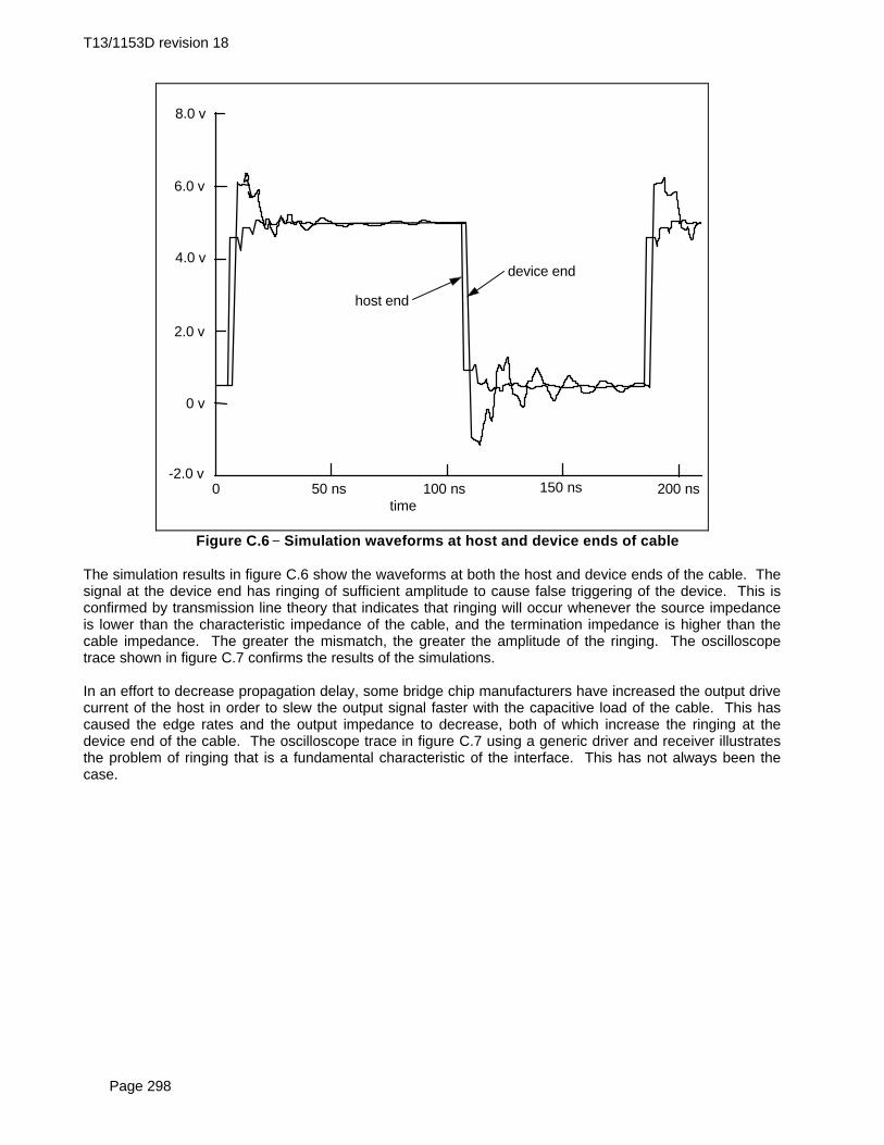
T13/1153D revision 18
Page 298
host end
device end
0 50 ns 100 ns 150 ns 200 nstime
-2.0 v
0 v
2.0 v
4.0 v
6.0 v
8.0 v
Figure C.6 −− Simulation waveforms at host and device ends of cable
The simulation results in figure C.6 show the waveforms at both the host and device ends of the cable. Thesignal at the device end has ringing of sufficient amplitude to cause false triggering of the device. This isconfirmed by transmission line theory that indicates that ringing will occur whenever the source impedanceis lower than the characteristic impedance of the cable, and the termination impedance is higher than thecable impedance. The greater the mismatch, the greater the amplitude of the ringing. The oscilloscopetrace shown in figure C.7 confirms the results of the simulations.
In an effort to decrease propagation delay, some bridge chip manufacturers have increased the output drivecurrent of the host in order to slew the output signal faster with the capacitive load of the cable. This hascaused the edge rates and the output impedance to decrease, both of which increase the ringing at thedevice end of the cable. The oscilloscope trace in figure C.7 using a generic driver and receiver illustratesthe problem of ringing that is a fundamental characteristic of the interface. This has not always been thecase.

T13/1153D revision 18
Page 299
5 V
0 V
50 ns/div horizontal 1 V/div vertical
Figure C.7 −− Oscilloscope trace at device end of DIOR- signal on a typical system
C.2.2 What are the options?
The proper solutions are to terminate the transmission line and limit the frequency range of the signals.There are two termination possibilities: series or source, and parallel or load. Unfortunately, each of thesesolutions has problems of its own, and, regardless of the method of termination, ringing occurs in two-deviceconfigurations. The input impedance of devices is not infinite: they appear as a reactive load due as theinput capacitance forms transmission line discontinuities.
Source termination is suited to situations where the signal is received at the far end of the line, and not in-between. But devices can be placed anywhere along a cable. The signals at the device in the middle of thecable have an initial step in their edges due to the series termination. Another problem with sourcetermination is devices are not necessarily at one end of the cable.
Load termination has different problems. A 110 ohm termination at the device end causes excessive DCloading. The SCSI interface standard avoids ringing by requiring terminations at each end of the physicalcable and having each device drive the cable with a current sink. However, SCSI configurations often havetoo many, too few, or improperly located terminations. Changing this standard to a user-installedtermination scheme loses all backward compatibility and is therefore not considered to be a viable option.
One of the solutions used in the past to “fix” failing configurations has been to place a capacitor at the inputof the device. Since the ringing is the result of a resonant system, adding purely reactive elements(capacitors and inductors) that simply change the frequency of oscillation is not recommended. Theseelements may fix a given configuration of a device and cable, but they really just move the interferingresonance peaks to a different frequency, solving the problem only for that particular configuration. Propersolutions include resistive elements to dissipate the energy stored in the transmission line.
No single solution meets the dual criteria of solving the ringing problem and being backward compatible withcurrent systems. The suggested approach uses partial solutions in three different areas: partial terminationat the host, partial termination at the device, and edge rate control at both the host and the device.
C.2.3 Design goals
Before a solution can be designed the design goals must be explicitly stated. This leads to the question of“How much ringing is acceptable?” To answer this question the design and specification of the bus must beconsidered.

T13/1153D revision 18
Page 300
The bus was originally designed to use standard TTL signals. TTL was designed with built-in noise margin.All drivers are required to have a “low” (zero) signal level of 0.5 V or less, and a “high” (one) signal level of2.4 V or more. All receivers are specified to accept any signal below 0.8 V as a logical zero and any signalabove 2.0 V as a logical one. This results in a low-side noise margin of 0.3 V (0.8 - 0.5) and a high-sidemargin of 0.4 V (2.4 - 2.0). Signals between 0.8 V and 2.0 V are in no man’s land, interpreted by thereceiver as either a zero or a one. TTL compatible inputs typically use a switching threshold of 1.3 to 1.4 V.
Bus designers have long known that the noise margins of TTL are insufficient for signals passed on cables.To improve the noise margin inherent in TTL systems, hysteresis has been added to the receiver input.Hysteresis changes the input switching threshold depending on the present state of the logic output of thereceiver. For example, if the receiver is currently in a zero state, it might require an input voltage of 1.7 Vbefore changing to a one. Once in a one state, the receiver might require the input voltage to drop below0.9 V before changing back to a zero. Modern design practice dictates that all signals passing across a busbe received with hysteresis.
It is desirable that, even with ringing, the input signal remain less than 0.5 V after a falling edge and remainabove 2.4 V after a rising edge. With CMOS drivers only the falling edge is of concern. This is due to theinput switching threshold of TTL (typically 1.4 V) being closer to ground than to the supply. It turns out thatdesigning to the 0.5 V requirement is too restrictive, so the looser requirement of 0.8 V is used here. Thisrelaxed requirement removes the noise margin inherent in TTL and depends on receiver hysteresis forproper operation. As input hysteresis has been the norm in device design for many years now, thislimitation is not considered unreasonable.
Depending on system timing and other issues, a designer may elect to use a looser threshold of 0.9 V or atighter one of 0.7 V. For these cases circuit simulation of the bus and receiver is done to verify the design.The resulting termination circuits have different values from those derived here.
C.2.4 Source termination
A series resistor at the source (host) acts as a termination to the transmission line. When the value of theresistor matches the characteristic impedance of the cable (110 ohms) then the reflection returning from theload is reduced to zero. Resistor values less than the characteristic impedance will partially terminate thecable and reduce the reflection.
NOTE − This assumes that the output impedance of the driver is zero. In reality, anoptimum match occurs when the output impedance and the series resistor together equalthe cable impedance. This also assumes that the host is at the end of the cable. If it is inthe middle of the cable, then it sees two cables in parallel and the optimum impedancematch would be 55 ohms.
This standard requires that a source be able to sink 4 mA while maintaining a logical low output voltage of0.5 V or less (see 4.3). For a TTL output the low output voltage is a combination of the saturation voltageand resistance of the pulldown transistor. For a CMOS output the pulldown transistor has no saturationvoltage and is just a resistance. Adding a series resistor in the output of the driver causes the output logicalzero voltage to increase with greater resistance. For example, if the unterminated logical zero output of thedriver is 0.4 V, then a maximum series resistance of 25.0 ohms would be allowed ( (0.5-0.4)/4mA ). ThisDC voltage drop requirement acts in opposition to the higher resistance values required for cabletermination.
If it is assumed that an unterminated CMOS output driver can drive a logical low to 0.3 V at the rated sinkcurrent, then there is a 0.2 V to drop across the series resistor. This gives a maximum resistor value of 50ohms. So the value of the series resistor depends on the CMOS output, the logical zero voltage, and thesink current.
Another consideration in selecting the value of the series resistor is the initial voltage on an edge. Assumea step function voltage source driving a transmission line through a series resistor. The initial amplitude ofthe edge at the input of the line is a voltage divider of the series resistor and the characteristic impedance.

T13/1153D revision 18
Page 301
A receiving device can be near the source and the edge must go through logic thresholds. The worst caseis a negative edge from 5 V and a control line of 110 ohms impedance. The attenuation of the voltagedivider must be small enough to allow the edge to cross from 5 V through 0.8 V. Assuming that the leadingedge will just reach 0 V at the source, An analysis shows the series resistor must be no larger than 21 ohmsto meet this ( (5.0)/(5.0-0.8)=(110+R)/110 ). The closest standard five-percent value is 22 ohms. If oneassumes that the leading edge will undershoot to 0.5V at the source, the resistor may be no larger than 33ohms.
Is a 22 or 33 ohm resistor adequate for reducing the ringing? The simulation was repeated using the samemodel as shown in figure C.5 with a 33 ohm series resistor added. The results of that simulation appear infigure C.8. The ringing is significantly reduced from the previous simulation in figure C.6. Simulations werealso performed on the model using a 22 ohm source resistor and similar reduction in ringing was observed.
0 50 ns 100 ns 150 ns 200 ns
time
-2.0 v
0 v
2.0 v
4.0 v
6.0 v
8.0 v
host end
device end
Figure C.8 −− Waveforms with 33 ohm series resistor at source
For data lines there are two factors that make the considerations for selecting the series resistor significantlydifferent. First, the characteristic impedance of a data line is higher since ground lines are farther away.Second, data lines are not edge sensitive, data settling time is the issue. The value of the series resistor islimited by the DC loading requirements, not the edge integrity. Adoption of this standard for DC loadingallows further increase of the series resistance since the DC loading is the limiting factor. The characteristicimpedance of lines adjacent to ground wires is the lowest of the data lines and is about 160 ohms; a highervalue of series resistance is necessary to dampen reflections.
C.2.5 Receiver termination
Device termination is more difficult than host termination. Viable solutions must work with one or twodevices located anywhere along the cable. The host may or may not have termination. These and otherconsiderations make device termination a multifaceted problem.
T13/1153D revision 18
Page 302
The first constraint is the maximum DC loading allowed. This standard requires that the host be capable ofproviding 400 µA of current while in a logical one state. Assuming each device is allowed to take half of thatamount, the minimum DC resistance allowed is 25K ohms.
NOTE − This assumes a CMOS output with a high output voltage of 5.0 V : 5.0 V/200 µA =25 KΩ
For a 110 ohm transmission line, 25K ohms is as good as infinity. This means that any practical terminationsolution must not have significant DC loading.
One way of terminating the cable is with an “AC termination.” This is a simple RC network that providestermination for high-frequency signals but does not load the line at DC (see figure C.9). This circuit acts asboth a cable termination and a filter for the ringing. The termination characteristics can be observed bylooking at the ringing signal at the host when the circuit is connected or removed. When the circuit is inplace, less energy is reflected back to the host, so the host waveform has less ringing. The lowpass filtercharacteristics of the circuit help decrease the amount of ringing presented to the interface circuitry of thedevice.
Although this may appear to be an unusual method of terminating the cable, it is not without precedent. TheIEEE P996 committee recognized the problems inherent in the design of the IBM PC/AT bus andrecommended a series RC termination for increased “data integrity and system reliability.” They suggestedthat the termination circuit be added to each end of the backplane or motherboard. The recommendedvalues are 40 to 60 ohms for the resistor and 30 to 70 pf for the capacitor.
Deriving the optimum values for a bus AC termination circuit is difficult. The easiest way of determining thevalues is to perform a number of trial-and-error SPICE simulations for different host and deviceconfigurations. The recommended values are 82 ohms and 10 pf. Simulations show that capacitancevalues between 8 pf and 20 pf work well. Since the input capacitance of many interface chips is between 8and 10 pf, a discrete capacitor is often unnecessary. This reduces the cost of implementation on the device.A conservative approach is to place pads so additional capacitance can be added if required.
Device manufacturers need to ensure that any partial termination circuits they implement present aneffective capacitance of 20 pf or less. What is an effective capacitance? From a practical point of view,any circuit is valid provided it does not increase the propagation delay of a worst-case cable. This isbecause systems manufacturers are counting on a certain cable delay in their design. The easiest way toanswer the question of acceptability is to run a SPICE simulation and measure the delay. The simulationshould be run twice: once with a simple 20 pf load, and again with the proposed termination circuit. If theresulting delay of the proposed termination circuit is less than or equal to that obtained with a 20 pf load,then it meets the criterion for acceptance. The recommended termination of 82 ohms and 10 pf passes thetest.
The major drawback of the RC termination circuit is that it adds delay to the signal. Since this standarddefines the timing at the input to the device (see clause 10), device manufacturers must ensure that theirinterface chip still works properly with the additional delay. The delay can be calculated for rising edges (2.0V threshold) and falling edges (0.8 V threshold) with a fairly straightforward SPICE simulation. For the 82ohm and 10 pf termination the delay is less than 1.5 ns (0.7 ns for the rising edge, 1.2 ns for the fallingedge, derived from simulations ).
Will termination at both the host and the device “over-terminate” the transmission line? Figure C.10 showsthe simulation results for device termination with no host termination, and figure C.11 shows the samesimulation with a 33 ohm host termination added. It is clear that termination at both the host and the deviceresults in the best signal integrity.
Another option for controlling ringing at the device is the use of a clamping circuit. Biased diodes have beenshown to be excellent solutions, reducing the ringing to virtually zero. The advantage of clamp circuits isthat they do not require any components in series with the signal, and therefore do not add any delay. Thisis particularly important for PIO mode 4 operation. The disadvantage of clamping circuits is that they takeconsiderably more space on the circuit board and cost much more than passive elements. Some
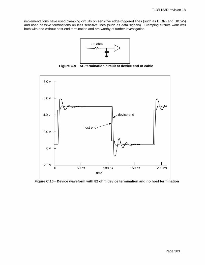
T13/1153D revision 18
Page 303
implementations have used clamping circuits on sensitive edge-triggered lines (such as DIOR- and DIOW-)and used passive terminations on less sensitive lines (such as data signals). Clamping circuits work wellboth with and without host-end termination and are worthy of further investigation.
82 ohm
Figure C.9 −− AC termination circuit at device end of cable
host end
device end
0 50 ns 100 ns 150 ns 200 nstime
-2.0 v
0 v
2.0 v
4.0 v
6.0 v
8.0 v
Figure C.10 −− Device waveform with 82 ohm device termination and no host termination
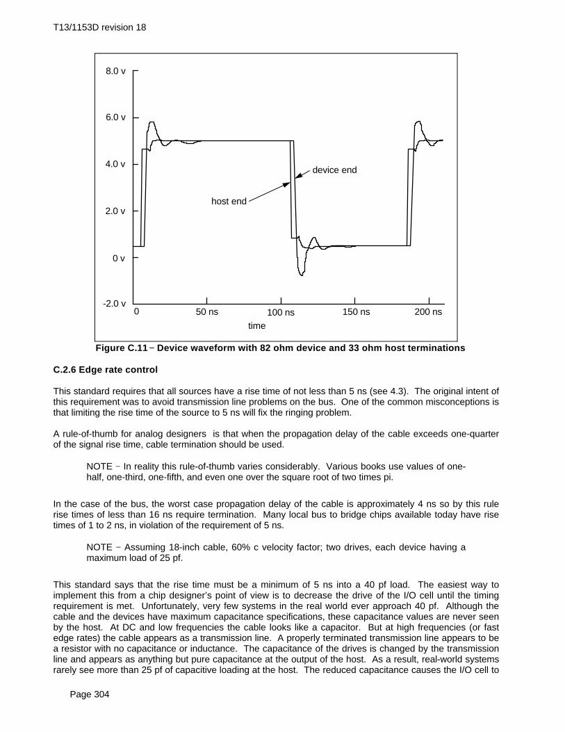
T13/1153D revision 18
Page 304
host end
device end
0 50 ns 100 ns 150 ns 200 nstime
-2.0 v
0 v
2.0 v
4.0 v
6.0 v
8.0 v
Figure C.11 −− Device waveform with 82 ohm device and 33 ohm host terminations
C.2.6 Edge rate control
This standard requires that all sources have a rise time of not less than 5 ns (see 4.3). The original intent ofthis requirement was to avoid transmission line problems on the bus. One of the common misconceptions isthat limiting the rise time of the source to 5 ns will fix the ringing problem.
A rule-of-thumb for analog designers is that when the propagation delay of the cable exceeds one-quarterof the signal rise time, cable termination should be used.
NOTE − In reality this rule-of-thumb varies considerably. Various books use values of one-half, one-third, one-fifth, and even one over the square root of two times pi.
In the case of the bus, the worst case propagation delay of the cable is approximately 4 ns so by this rulerise times of less than 16 ns require termination. Many local bus to bridge chips available today have risetimes of 1 to 2 ns, in violation of the requirement of 5 ns.
NOTE − Assuming 18-inch cable, 60% c velocity factor; two drives, each device having amaximum load of 25 pf.
This standard says that the rise time must be a minimum of 5 ns into a 40 pf load. The easiest way toimplement this from a chip designer’s point of view is to decrease the drive of the I/O cell until the timingrequirement is met. Unfortunately, very few systems in the real world ever approach 40 pf. Although thecable and the devices have maximum capacitance specifications, these capacitance values are never seenby the host. At DC and low frequencies the cable looks like a capacitor. But at high frequencies (or fastedge rates) the cable appears as a transmission line. A properly terminated transmission line appears to bea resistor with no capacitance or inductance. The capacitance of the drives is changed by the transmissionline and appears as anything but pure capacitance at the output of the host. As a result, real-world systemsrarely see more than 25 pf of capacitive loading at the host. The reduced capacitance causes the I/O cell to
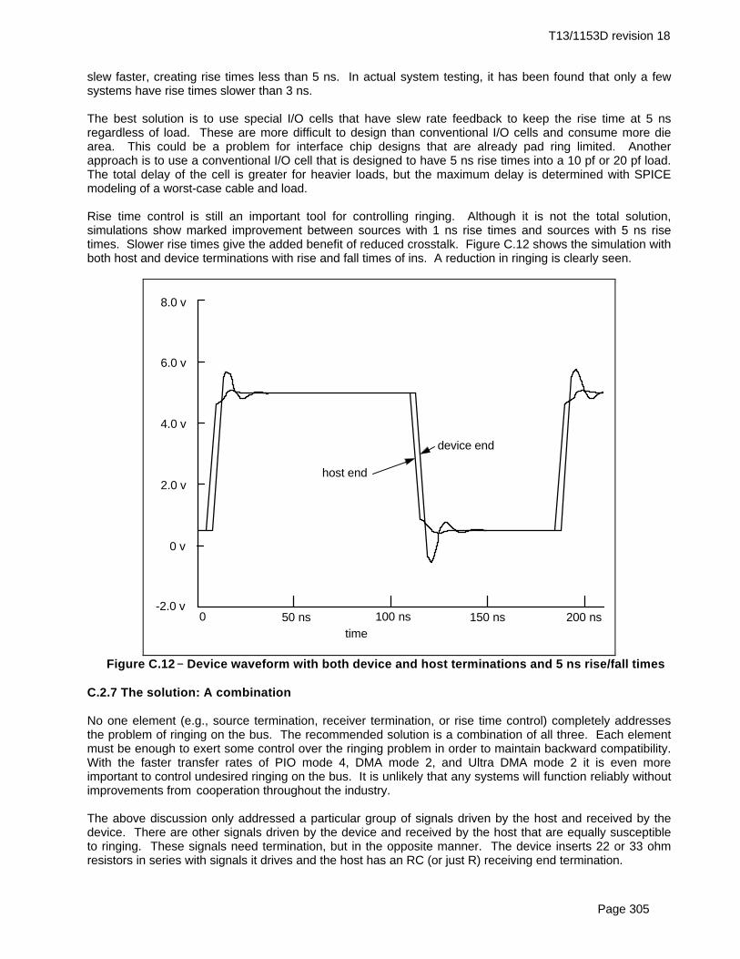
T13/1153D revision 18
Page 305
slew faster, creating rise times less than 5 ns. In actual system testing, it has been found that only a fewsystems have rise times slower than 3 ns.
The best solution is to use special I/O cells that have slew rate feedback to keep the rise time at 5 nsregardless of load. These are more difficult to design than conventional I/O cells and consume more diearea. This could be a problem for interface chip designs that are already pad ring limited. Anotherapproach is to use a conventional I/O cell that is designed to have 5 ns rise times into a 10 pf or 20 pf load.The total delay of the cell is greater for heavier loads, but the maximum delay is determined with SPICEmodeling of a worst-case cable and load.
Rise time control is still an important tool for controlling ringing. Although it is not the total solution,simulations show marked improvement between sources with 1 ns rise times and sources with 5 ns risetimes. Slower rise times give the added benefit of reduced crosstalk. Figure C.12 shows the simulation withboth host and device terminations with rise and fall times of ins. A reduction in ringing is clearly seen.
host end
device end
0 50 ns 100 ns 150 ns 200 nstime
-2.0 v
0 v
2.0 v
4.0 v
6.0 v
8.0 v
Figure C.12 −− Device waveform with both device and host terminations and 5 ns rise/fall times
C.2.7 The solution: A combination
No one element (e.g., source termination, receiver termination, or rise time control) completely addressesthe problem of ringing on the bus. The recommended solution is a combination of all three. Each elementmust be enough to exert some control over the ringing problem in order to maintain backward compatibility.With the faster transfer rates of PIO mode 4, DMA mode 2, and Ultra DMA mode 2 it is even moreimportant to control undesired ringing on the bus. It is unlikely that any systems will function reliably withoutimprovements from cooperation throughout the industry.
The above discussion only addressed a particular group of signals driven by the host and received by thedevice. There are other signals driven by the device and received by the host that are equally susceptibleto ringing. These signals need termination, but in the opposite manner. The device inserts 22 or 33 ohmresistors in series with signals it drives and the host has an RC (or just R) receiving end termination.

T13/1153D revision 18
Page 306
The data lines are different in several ways. First, they must move data bidirectionally. Second, they arenot edge sensitive, ringing affects the settling time. Third, since there are no ground wires between datalines in an ATA cable, the data lines are highly coupled. Fourth, the transmission line characteristicimpedances are higher than strobe lines since ground wires are farther away. These differences demandother considerations than the previous treatment.
Since data lines are bidirectional, the terminations on drives and host should be the same. For settling time,the ringing frequency and its rate of decay, or Q factor, are the concerns. The mutual coupling among datalines affects the ringing frequency causing it to be lower. The higher characteristic impedance causes therate of decay of ringing to be slower since the Q factor is higher. Controlling the resistance in the data lineshelps by limiting the Q factor, peak currents, and decay rate of the ringing. Controlling the load capacitancelimits the frequency of the ringing.
Improper treatment of the data lines has several bad effects. Data settling time can increase to as long as45 ns in severe cases. Excessive ringing on the data lines can induce spurious signals on adjacent controllines (crosstalk to DIOW- or RESET-).
Good design dictates that some type of ringing control be used on data lines, but of a different type than oncontrol lines. A good practice is to insert 33 ohm series resistors on data lines at both the host and thedevice. The maximum capacitance specification in this standard must be met. The trace lengths from theload to the connector of the device or host board should be short. The driving end sees the same sourcetermination as before. The receiving end sees an RC network of 33 ohms combined with the inputcapacitance of the interface chip. This is enough to substantially reduce the ringing and minimize settlingtime.
The IORDY line is a unique case on the bus. Under PIO modes it is driven by an open collector outputsfrom the device, a current source rather than a voltage source. The nature of this signal makes it relativelyinsensitive to ringing that might occur. However, in Ultra DMA the IORDY line is used as a high speed datastrobe from the device to the host. Termination of IORDY is recommended.
The one remaining bus structure not discussed is the open collector output driven by the device (DASP-).This signal is driven by a current source rather than a voltage source. Usually the transistor driving thissignal is relatively slow and does not cause an excessive amount of ringing. The nature of DASP- makes itrelatively insensitive to ringing that might occur.
Table C.1 summarizes the typical termination values:
Table C.1 −− Typical terminationSignal Name Host Termination Device TerminationDIOR-, DIOW- 22 ohm series 82 ohm series
CS0-, CS1- 33 ohm series 82 ohm seriesDA0, DA1, DA2 33 ohm series 82 ohm series
DMACK- 22 ohm series 82 ohm seriesRESET- 33 ohm series 82 ohm series
DD0 through DD15 33 ohm series 33 ohm seriesDMARQ 82 ohm series 22 ohm seriesINTRQ 82 ohm series 22 ohm seriesIORDY 82 ohm series 22 ohm series
DASP-, PDIAG- no change no changeCSEL no change no change
NOTE − For the 82 ohm series termination, an additional parallel capacitor may be neededif the interface chip and circuit board layout have less than 8 pf of capacitance.
C.2.7.1 Example of device-end termination timing
Assume that 82 ohm series resistors are inserted on all receive signals and 22 or 33 ohm series resistors onall transmit and bidirectional signals. Also assume that the input capacitance of the interface chip is 10 pf.

T13/1153D revision 18
Page 307
There are three different RC configurations that occur (see figure C.13). All receive signals will see an 82ohm and 10 pf network. The data lines will see a 33 ohm and 10 pf network when the device is receivingdata. Signals driven back to the host (including data lines during a read) will see 33 ohms and 50 pf. The50 pf assumption is the worst-case condition of both the host and another device being located nearby(negligible cable length), and both of them having the maximum allowed input capacitance.
Control Signal(e.g.,DIOR-,CS0-)
82 ohm
10 pf
Drive
Data Line(Write Cycle)
33 ohm
10 pf
Drive
Data Line(Read Cycle)
33 ohmDrive
50 pf
Figure C.13 −− Signal models for device-end timing calculations
A simple SPICE simulation with a signal source and an RC load will show what the delays are through thesethree networks. Because the switching thresholds are not symmetrical with respect to the supply (0.8 V and2.0 V) the delay for rising edges is different than that for falling edges. Since the input edge rate isunknown, both fast and slow edge inputs are simulated. The worst-case delay occurs with slow edges forrise times and fast edges for fall times. This mixture of slow rise time and fast fall time does not occur inreal life, but since the edge speed is not known the worst case is planned for. The SPICE signal source isprogrammed for a rise time of 6.25 ns (same as 5 ns for 10% to 90%) and a fall time of 0.1 ns. The netresult is six delay values. The results of the SPICE simulations are shown in table C.2.
Table C.2 −− Typical device-end propagation delay timesSymbol Description Value
Tphlc Propagation delay, high to low, control line 1.0 nsTplhc Propagation delay, low to high, control line 0.9 nsTphldi Propagation delay, high to low, data in 0.5 nsTplhdi Propagation delay, low to high, data in 0.3 nsTphldo Propagation delay, high to low, data out 2.5 nsTplhdo Propagation delay, low to high, data out 1.1 ns
These delay values, combined with the interface chip timing specifications, will give the timing at the pins ofthe device. The trick is to figure out how each one of the timing parameters is affected by the delays.
For example, consider the DIOW- Data Setup time (value t3). This is the amount of time that the data mustbe stable before the rising edge of DIOW-. Assume that the interface chip has a value of 2.0 ns. It isknown that DIOW- is a control signal and the rising edge of control signals are delayed by 0.9 ns. Thismeans that the setup time at the chip is actually greater than expected, but the data is delayed, too. It is notknown what the data pattern is so it is assumed that the delay time is the maximum of Tphldi and Tplhdi.The actual setup time is 2.0 + 0.9 - MAX(0.3, 0.5) = 2.4 ns. This is less than the requirement of 30 ns (forPIO mode 3) and therefore within spec.
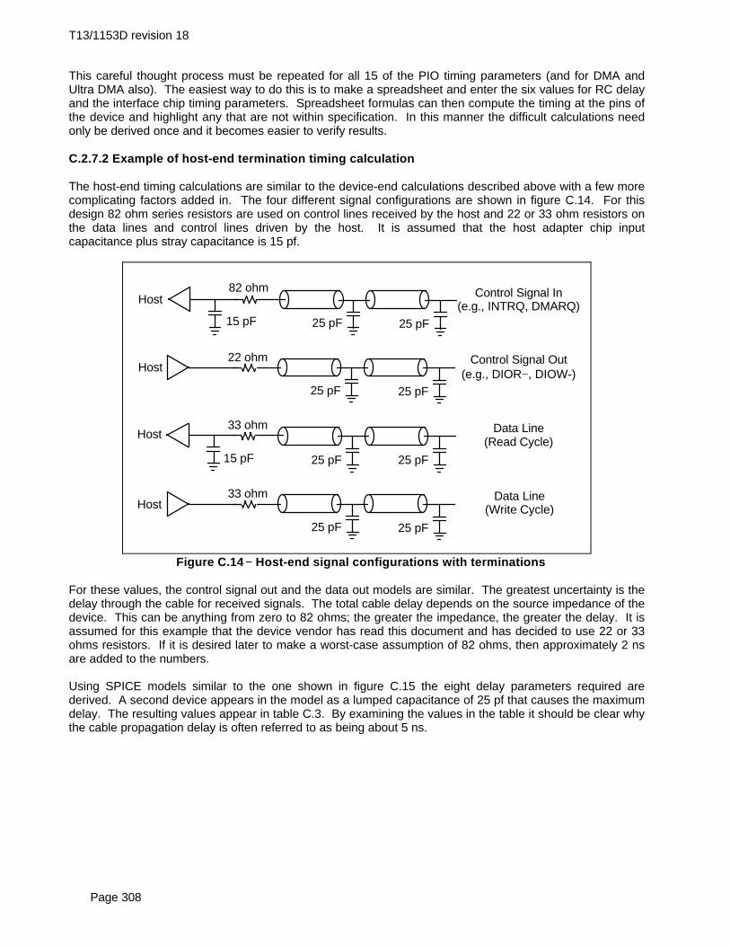
T13/1153D revision 18
Page 308
This careful thought process must be repeated for all 15 of the PIO timing parameters (and for DMA andUltra DMA also). The easiest way to do this is to make a spreadsheet and enter the six values for RC delayand the interface chip timing parameters. Spreadsheet formulas can then compute the timing at the pins ofthe device and highlight any that are not within specification. In this manner the difficult calculations needonly be derived once and it becomes easier to verify results.
C.2.7.2 Example of host-end termination timing calculation
The host-end timing calculations are similar to the device-end calculations described above with a few morecomplicating factors added in. The four different signal configurations are shown in figure C.14. For thisdesign 82 ohm series resistors are used on control lines received by the host and 22 or 33 ohm resistors onthe data lines and control lines driven by the host. It is assumed that the host adapter chip inputcapacitance plus stray capacitance is 15 pf.
Control Signal In(e.g., INTRQ, DMARQ)
Control Signal Out(e.g., DIOR−, DIOW-)
Data Line(Read Cycle)
Data Line(Write Cycle)
Host
Host
Host
Host
82 ohm
15 pF
22 ohm
15 pF
33 ohm
33 ohm
25 pF 25 pF
25 pF 25 pF
25 pF 25 pF
25 pF 25 pF
Figure C.14 −− Host-end signal configurations with terminations
For these values, the control signal out and the data out models are similar. The greatest uncertainty is thedelay through the cable for received signals. The total cable delay depends on the source impedance of thedevice. This can be anything from zero to 82 ohms; the greater the impedance, the greater the delay. It isassumed for this example that the device vendor has read this document and has decided to use 22 or 33ohms resistors. If it is desired later to make a worst-case assumption of 82 ohms, then approximately 2 nsare added to the numbers.
Using SPICE models similar to the one shown in figure C.15 the eight delay parameters required arederived. A second device appears in the model as a lumped capacitance of 25 pf that causes the maximumdelay. The resulting values appear in table C.3. By examining the values in the table it should be clear whythe cable propagation delay is often referred to as being about 5 ns.

T13/1153D revision 18
Page 309
R722
T2 Device 0
V1Tr = 0.1 nsTf = 0.1 ns
TD = 1.5 nsZ0 = 110
Host Cable
C225 pf
T3 Device 1
TD = 1.0 nsZ0 = 110
Cable
C325 pf
Figure C.15 −− SPICE model for control signal out delay calculation
Table C.3 −− Typical host-end propagation delay timesSymbol Description ValueTphlci Propagation delay, high to low, control in 6.4 nsTplhci Propagation delay, low to high, control in 4.7 nsTphlco Propagation delay, high to low, control out 5.9 nsTplhco Propagation delay, low to high, control out 4.6 nsTphldi Propagation delay, high to low, data in 5.7 nsTplhdi Propagation delay, low to high, data in 4.3 nsTphldo Propagation delay, high to low, data out 5.9 nsTplhdo Propagation delay, low to high, data out 4.6 ns
The process of finding the timing values is the same as for the device-end example. The propagation delaytimes are added to and subtracted from the host adapter chip timings to obtain the timings at the input to thedevice, in this case calculating the timing at the device furthest from the host adapter. The resulting timingvalues are compared against the values to determine what mode the device operates at.
C.2.8 Dual port cabling
One of the recent enhancements to the bus has been the use of primary and secondary ports, allowing theuser to attach up to four devices. The optimal way to implement dual ports is to have two completelyseparate interfaces that have no circuitry in common. This guarantees isolation between the ports andinsures that no interference will occur.
The advent of local bus bridge chips has introduced new driving forces to the dual port cabling issue.Implementing two independent ports on a single chip requires 66 I/O pins. Due to the cost of pins, somedesigns have combined the data lines of the two ports into one set of pins. Sharing the data lines (or anyother lines) in this way without termination allows the two cables and devices attached to interact.Simulations confirm that the ringing in such configurations is large and complex, particularly if the loads onthe two cables are not balanced. Even with termination the buffer output impedance is a consideration.
One alternative pin-saving solution would be to add a set of external buffers such as the 74ALS245. Thiswould require three new control lines but would save 16 data lines for a net improvement of 13 pins. Thisalso would require additional packages on the circuit board.
An economical solution is to add independent series resistors for each line (see figure C.16). Energyreflected back from the first cable passes through a series termination resistor, the shunt output impedanceof the driver, a second series resistor and then into the second cable before getting to the host. This signal isreflected from the end of the second cable (with loss), and must pass through the termination resistor againbefore arriving at the host. The two series terminations and the shunt impedance of the buffer at the host

T13/1153D revision 18
Page 310
forms a T attenuator network isolating the two cables. The effectiveness of this network depends on thevalues: the series resistors need to be large, the shunt needs to be small, and the traces need to be short.The drivers must have high capacity to drive two cables, and additionally to attenuate ringing from onecable to the other. This provides sufficient attenuation of reflected signals to make ringing not a problem ifall specifications are met, and all recommended terminations and trace lengths are implemented. Whensome recommendations and specifications are not met, the situation is more uncertain.
In practice, configurations will have devices that do not follow these recommendations. Nevertheless, it isreasonable to expect all manufacturers to conform to the ATA specification. Extensive simulation work hasbeen done assuming specification conformance, and configurations that have at least one conformingdevice. The design of the host is a key factor in the performance of dual cable configurations.
Proving that any scheme works is a significant task. Simulations must be performed for all combinations ofone device vs. two devices, devices with terminations and devices without terminations, devices with littleload capacitance and maximum load capacitance, differing data patterns, etc. With two ports the number ofcombinations is daunting. Simulations have not yet revealed a combination of devices that fails to operateproperly. Simulation results have been spot checked against actual systems.
Primary PortDevice 0 Device 1
33 ohm
Device 0 Device 1
Secondary Port
Figure C.16 −− Preferred connection for shared lines in dual port systems
Not all of the signal lines in a shared dual port interface can be shared. If the chip select lines (CS0-, CS1-)and the data strobe lines (DIOR-, DIOW-) are shared, then it is impossible to differentiate between theprimary and secondary ports. A write to a device on one port causes the same action to occur on the otherport, destroying the data on the other device. The data strobe lines are sensitive edge-triggered signalswhile the chip select lines act more like level-sensitive address lines. It is recommended that designersshare the less sensitive chip select lines and not share the data strobe lines.
The purpose of the chip select lines is to select the active device. It makes sense to have independent chipselect lines for primary and secondary ports. This allows the DIOR- and DIOW- lines to be shared. TheATA bus signals that can and cannot be shared are shown in table C.4.
Table C.4 makes some assumptions about how the dual porting is being implemented. If the data lines areshared, there can not be simultaneous accesses to the primary and secondary ports. The IORDY linecannot be shared since it is a strobe in Ultra DMA mode and because of transmission line considerations.The INTRQ and DMARQ signals are driven by tristate buffers on the devices. Either Device 0 or Device 1enables its tristate driver depending on the state of the DEV bit in the Device/Head Register. ThereforeINTRQ and DMARQ cannot be shared because either Device 0 or Device 1 will be driving these lines at alltimes. The primary port devices do not know about the secondary port devices, so sharing these lineswould create a conflict. In theory, the DMACK- line could be shared since it is driven by the host. Inpractice this is not recommended. It is likely that some devices respond unconditionally to the DMACK-signal, whether they ever requested a DMA cycle or not. This could lead to a conflict on a DMA cyclebetween a primary port device and a secondary port device during the data cycle. For these reasons theINTRQ, DMARQ, and DMACK- lines cannot be shared.

T13/1153D revision 18
Page 311
Table C.4 −− Possible sharing of signals in dual port configurationsSignal name
DIOR-, DIOW- Not shareableCS0-, CS1- Shareable
DA0, DA1, DA2 ShareableDMACK- Not shareableRESET- Shareable
DD0 – DD15 ShareableDMARQ Not shareableINTRQ Not shareableIORDY Shareable
DASP-, PDIAG- Not shareableCSEL Not shareable
The DASP- lines cannot be shared. Assume there are two devices on the primary port, and one device onthe secondary port. With the DASP- lines connected, the single device on the secondary port will incorrectly“see” Device 1 on the primary port. This would be a problem for all manufacturers who follow thespecifications. Similar problems can occur with the PDIAG- lines; they cannot be shared.
Sharing lines between ports will lead to lower performance than fully independent ports. Newer operatingsystems are multithreaded, so it is possible for accesses to be occurring independently and concurrently onthe primary and secondary ports. With shared signals lines concurrent access is not possible, hence theimpact on performance.
Note that the entries in table C.4 are not the last word on line sharing. There are specific conditions underwhich some lines may be sharable. For example, if separate DIOR- and DIOW- lines were provided forprimary and secondary ports, then the CS0- and CS1- lines could be shared. Many combinations of sharedand non-shared lines are possible provided that the functionality of the signals is carefully considered.
C.3 Crosstalk
Crosstalk is switching on one signal line causing induced signals in an adjacent line. Crosstalk has not beena significant issue in the past with slower edge rates; in newer systems the problem is often masked byringing. Once the cable is terminated and the ringing is under control, then the presence of crosstalkbecomes apparent.
C.3.1 Coupling mechanisms
There are three mechanisms by which a signal couples into an adjacent line. The first is mutualcapacitance, the second is mutual inductance, and the third is common impedance coupling. As a switchingsignal wavefront propagates down the cable it couples energy into the adjacent line. Once this energy is inthe second transmission line, it propagates in both directions: forward toward the receiver and back towardthe source (see figure C.17).
First the forward coupling components are examined. The coupling capacitance between the two linecauses a current pulse in the secondary line proportional to the capacitance and the rate of change ofvoltage on the primary side. A positive voltage step on the primary line causes a positive voltage spike onthe secondary line at both source and load.
The voltage induced in the second transmission line is proportional to the coupling coefficient, theinductance, and the rate of change of current in the primary side. This induced potential appearslongitudinally and presents as a negative voltage at the load, and a positive voltage at the source.
An additional voltage appears in series with the load from the current carried in the ground or signal returnwire. This type of coupling is called common impedance since the voltage is coupled from an impedancecommon to the two circuits. Here, the common impedance is that of the signal return or ground wire, and it
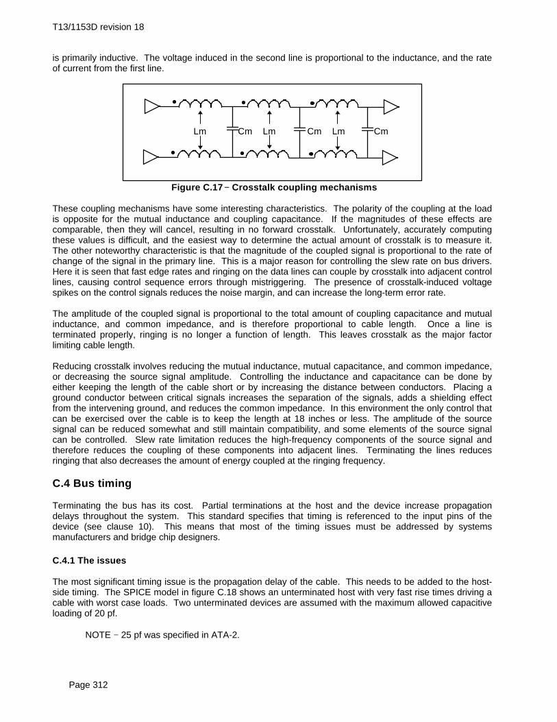
T13/1153D revision 18
Page 312
is primarily inductive. The voltage induced in the second line is proportional to the inductance, and the rateof current from the first line.
Lm Cm Lm Cm Lm Cm
Figure C.17 −− Crosstalk coupling mechanisms
These coupling mechanisms have some interesting characteristics. The polarity of the coupling at the loadis opposite for the mutual inductance and coupling capacitance. If the magnitudes of these effects arecomparable, then they will cancel, resulting in no forward crosstalk. Unfortunately, accurately computingthese values is difficult, and the easiest way to determine the actual amount of crosstalk is to measure it.The other noteworthy characteristic is that the magnitude of the coupled signal is proportional to the rate ofchange of the signal in the primary line. This is a major reason for controlling the slew rate on bus drivers.Here it is seen that fast edge rates and ringing on the data lines can couple by crosstalk into adjacent controllines, causing control sequence errors through mistriggering. The presence of crosstalk-induced voltagespikes on the control signals reduces the noise margin, and can increase the long-term error rate.
The amplitude of the coupled signal is proportional to the total amount of coupling capacitance and mutualinductance, and common impedance, and is therefore proportional to cable length. Once a line isterminated properly, ringing is no longer a function of length. This leaves crosstalk as the major factorlimiting cable length.
Reducing crosstalk involves reducing the mutual inductance, mutual capacitance, and common impedance,or decreasing the source signal amplitude. Controlling the inductance and capacitance can be done byeither keeping the length of the cable short or by increasing the distance between conductors. Placing aground conductor between critical signals increases the separation of the signals, adds a shielding effectfrom the intervening ground, and reduces the common impedance. In this environment the only control thatcan be exercised over the cable is to keep the length at 18 inches or less. The amplitude of the sourcesignal can be reduced somewhat and still maintain compatibility, and some elements of the source signalcan be controlled. Slew rate limitation reduces the high-frequency components of the source signal andtherefore reduces the coupling of these components into adjacent lines. Terminating the lines reducesringing that also decreases the amount of energy coupled at the ringing frequency.
C.4 Bus timing
Terminating the bus has its cost. Partial terminations at the host and the device increase propagationdelays throughout the system. This standard specifies that timing is referenced to the input pins of thedevice (see clause 10). This means that most of the timing issues must be addressed by systemsmanufacturers and bridge chip designers.
C.4.1 The issues
The most significant timing issue is the propagation delay of the cable. This needs to be added to the host-side timing. The SPICE model in figure C.18 shows an unterminated host with very fast rise times driving acable with worst case loads. Two unterminated devices are assumed with the maximum allowed capacitiveloading of 20 pf.
NOTE − 25 pf was specified in ATA-2.
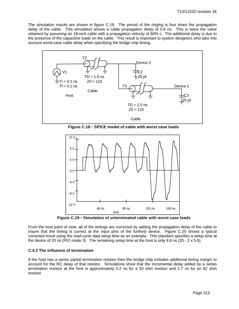
T13/1153D revision 18
Page 313
The simulation results are shown in figure C.19. The period of the ringing is four times the propagationdelay of the cable. This simulation shows a cable propagation delay of 5.6 ns. This is twice the valueobtained by assuming an 18-inch cable with a propagation velocity of 60% c. The additional delay is due tothe presence of the capacitive loads on the cable. This result is important to system designers who take intoaccount worst-case cable delay when specifying the bridge chip timing.
T2 Device 0
V1 C2 TD = 1.5 ns 25 pf Tr = 0.1 ns Z0 = 110 Tf = 0.1 ns T3 Device 1 Cable Host C3 25 pf TD = 1.5 ns Z0 = 110
Cable
Figure C.18 −− SPICE model of cable with worst case loads
12 V
8 V
4 V
0 V
-4 V
-8 V
-12 V 40 ns 80 ns 120 ns 160 ns time
Figure C.19 −− Simulation of unterminated cable with worst case loads
From the host point of view, all of the timings are corrected by adding the propagation delay of the cable toinsure that the timing is correct at the input pins of the furthest device. Figure C.20 shows a typicalcorrected result using the read cycle data setup time as an example. This standard specifies a setup time atthe device of 20 ns (PIO mode 3). The remaining setup time at the host is only 8.8 ns (20 - 2 x 5.6).
C.4.2 The influence of termination
If the host has a series partial termination resistor then the bridge chip includes additional timing margin toaccount for the RC delay of that resistor. Simulations show that the incremental delay added by a seriestermination resistor at the host is approximately 0.2 ns for a 33 ohm resistor and 1.7 ns for an 82 ohmresistor.

T13/1153D revision 18
Page 314
NOTE − Assuming a two device load, 25 pf at each device, an 18-inch cable, and 25 pf athost
The extra delay of higher resistor values is one of the reasons that 33 ohm series resistors at the host arerecommended.
DIOR- at host
5.6 ns 8.8 ns 5.6 ns
DIOR at device
20 ns
Data at device
5.6 ns
Data at host
Figure C.20 −− Host data setup time during a read cycle
The series resistor at the host is located as close as possible to the connector. To see the importance ofthis, SPICE simulations are done with the stray capacitance on the driver side of the series resistor andagain with the stray capacitance on the cable side. The ringing is reduced when the stray capacitance of thehost is on the driver side of the series resistor. A related issue is the distance from the host adapter chip (orchipset) to the connector. Some motherboards have the chip located up to 10 inches away from theconnector. This effectively adds another 10 inches to the 18-inch ribbon cable, resulting in an equivalentcable length of 28 inches.
NOTE − The traces on the circuit board are from 25 to 90 ohm impedance, so the electricallength of the trace cannot simply be added to the 110 ohm ribbon cable. A SPICEsimulation can be used to find the actual delay.
This additional length is not necessarily a problem. If the system manufacturer takes the extra trace delayinto account in the application of the host adapter chip, and the total capacitance is kept below the host limitof 25 pf, then in theory there is no difference. Real-world experience indicates that this calculation is rarelydone. The distance from the chip to the connector is not addressed in this standard. Keeping the connectorwithin 3 inches (by trace length) of the host adapter chip is recommended.
C.4.3 Calculating rise time
Chip designers often use a lumped capacitance model for simulating the delay of the output cell. For thesimulations this sometimes consists of adding the maximum capacitance allowed for the host and thedevices ((2 x 20) + (1 x 25) pf) to an estimated capacitance value for the cable (25 pf). Simulation is thenperformed with 100 pf capacitance on the output. This does not give an accurate measurement of thetiming. A better approximation is to use an output capacitance for the motherboard, a host end terminationresistor, and a transmission line to the devices (see figure C.21).
To illustrate how these models are different, suppose that the propagation delay of the output cell simulationis 2 ns too slow. The chip designer (using a 100 pf model) increases the drive current of the outputdevices. With enough drive current into a purely capacitive load, the 2 ns is removed, bringing the outputcell timing back into spec.

T13/1153D revision 18
Page 315
Increasing the drive of the output cell in the transmission line model, the length of the cable is not increasedand the speed of signal propagation in the cable is not increased. The 2 ns required time reduction is notachieved by increasing the output drive current. The time must come from somewhere else in the internalcircuitry. Increasing the output drive current only increases the edge speed, making the ringing worse at thedevice end (some time is gained with the faster edge speed, but not nearly as much as is predicted with asimple capacitive load model). It is not possible to decrease the overhead by increasing the drive current.
Most ASIC designers find that simulations using the recommended model of figure C.21 show their outputcells to be faster than in models with a 100 pf load.
+ −
+ −
T1 D6D1N4148
R4500 K
V35 V
Bufferunder test
TD = 2.5 nsZ0 = 110
C125 pf
D3D1N4148
R3500 K
T2
TD = 0.7 nsZ0 = 110
D5D1N4148
R7500 K
C425 pf
D4D1N4148
R6500 K
V45 V
Figure C.21 −− Recommended model for I/O cell propagation delay
C.4.4 Measuring propagation delay
Propagation delay times at the host (and at the device) are measured to the standard of 0.8 V for high to lowtransitions and 2.0 V for low to high transitions. Many IC manufacturers measure propagation delay at thetypical switch point for TTL of 1.4 V. This is not appropriate for the interface since virtually every chipmanufacturer (both host and device end) has included hysteresis for noise immunity. Since both thehysteresis window and hysteresis offset of a given receiver move with process, voltage, and temperature,the only guaranteed switch points are the TTL high and low values (0.8 V and 2.0 V).
C.5 Summary of guidelines
This summary is a collection of reminders for device, system, and chipset designers. They are separatedinto three groups by relevancy. The guidelines below are not intended to be a strict mandate, but a tool tohelp everyone build compatible, reliable, high-performance products.

T13/1153D revision 18
Page 316
C.5.1 Guidelines for device designers
− Terminate signals as shown in table C.1. Consider adding capacitors to ground on these lines if theinput capacitance is less than 8 pf, or use active clamping circuits. Place these resistors as close to theconnector as possible.
− Verify that the termination circuit used on received signals has less than 20 pf of equivalentcapacitance.
− Perform a timing analysis to verify that timings are met at the input to the device. Include the time delaydue to propagation and cable termination circuits.
C.5.2 Guidelines for system designers
− Do not use any value less than 1 K ohm for pull up resistors on open-collector signals such as IORDY(as per this standard).
− The host adapter chip should be located as close as possible to the connector. Keep the trace lengthbetween them less than 3 in.
− After circuit board fabrication, verify that the total input capacitance at the host is less than 25 pf.− Terminate signals as shown in table C.1. Place these resistors as close to the connector as possible.− Perform a system timing analysis to verify that timings are met at the input to the device.− For dual port implementations, terminate signals as shown in figure C.16. These resistors should be
placed as close to the connector of that port as possible.− For dual port implementations, the signal lines CS0- and CS1- may be shared, or the signals DIOR- and
DIOW- may be shared, but not both pairs.− For dual port implementations, do not share DASP- or PDIAG- signal lines.− For dual port implementations, perform a system timing analysis to verify that timings are met at the
input of the device. In particular watch the assertion widths of DIOR- and DIOW- to insure that theymeet the specification.
− Route cable away from chassis, power supplies, and high speed circuits.− Use the shortest cable practical and never greater than 18 in.
C.5.3 Guidelines for chip designers
− Design I/O cells to have rise and fall times of 5 ns or more under both minimum and maximum loadconditions.
− Perform timing simulations using a transmission line load model, not a 100 pf capacitor model.− Take worst-case cable delay into account when designing the interface. Ensure that timing can be met
at the device-end of the cable. Provide typical application data with timing for system manufacturers.

T13/1153D revision 18
Page 317
Annex D(informative)
Bibliography
AT Attachment Interface (ATA-1), ANSI X3.221-1994AT Attachment Interface with Extensions (ATA-2), ANSI X3.279-1996AT Attachment - 3, ANSI X3.298-1997BIOS Enhanced Disk Drive Specification (EDD), T13/1226DTATA Packet Interface (ATAPI) for Streaming Tape, QIC-1571
Suite of 2.5” Form Factor Specifications, SFF-8200, SFF-8201 2
Suite of 3.5” Form Factor Specifications, SFF-8300, SFF-8301, SFF-8302 2
ATA Packet Interface for CD-ROMs, SFF-8020i2
ATAPI Removable Rewritable Media, SFF-8070 2
ATAPI CD-R/RW Devices, SFF-80802
Commands for DVD Devices, SFF-80902
CompactFlash Association Specification Revision 1.2 3
1) QIC documents are published by:Quarter-Inch Cartridge Drive Standards, Inc.311 East Carrillo StreetSanta Barbara, CA 93101Tel: 805-963-3853Fax: 805-962-1541
2) SFF documents are published by:SFF14426 Black Walnut Court, Saratoga, California 95070FaxAccess: 408 741-1600
SFF documents may be obtained from:Global Engineering15 Inverness Way EastEnglewood, CO 80112-5704Tel: 303-792-2181 or 800-854-7179Fax: 303-792-2192
3) The CFA specification is published by:CompactFlash AssociationP.O. Box 51537Palo Alto, CA 94303http://www.compactflash.org

T13/1153D revision 18
Page 318
Annex E(informative)
Command set summary
The following four tables are provided to facilitate the understanding of the command set. Table E.1provides information on which command codes are currently defined. Table E.2 provides a list of all of thecommands in order of command code. Table E.3 provides a summary of all commands with the protocol,required use, command code, and registers used for each. Table E.4 shows the status and error bits used byeach command.
Table E.1 −− Command matrixx0 x1 x2 x3 x4 x5 x6 x7 x8 x9 xA xB xC xD xE xF
0x C R R C* R R R R C* R R R R R R R1x O E* E* E* E* E* E* E* E* E* E* E* E* E* E* E*2x C C O* O* R R R R R R R R R R R R3x C C O* O* R R R R C* R R R O* R R R4x C C R R R R R R R R R R R R R R5x O* R R R R R R R R R R R R R R R6x R R R R R R R R R R R R R R R R7x C E* E* E* E* E* E* E* E* E* E* E* E* E* E* E*8x V V V V V V V F* V V V V V V V V9x C C C R E* E* E* E* E* E* V R R R R RAx C* C* C* R R R R R R R R R R R R RBx C R R R R R R R R R R R R R R RCx F* V V V C C C C* C C C C C* C* R RDx R R R R R R R R R R C* E* E* E* C* C*Ex C C C C C C C C* C E* R R C* C* O* CFx V C C C C C C V C C* V V V V V V
Key:C = a defined command, R = Reserved, undefined in current specifications, V = Vendor specificcommandsO = Obsolete, E=a retired command, F=If the device does not implement the CFA feature set, thiscommand code is Vendor specific, * indicates that the definition of this command has changed from ATA-3, X3.298-1997.
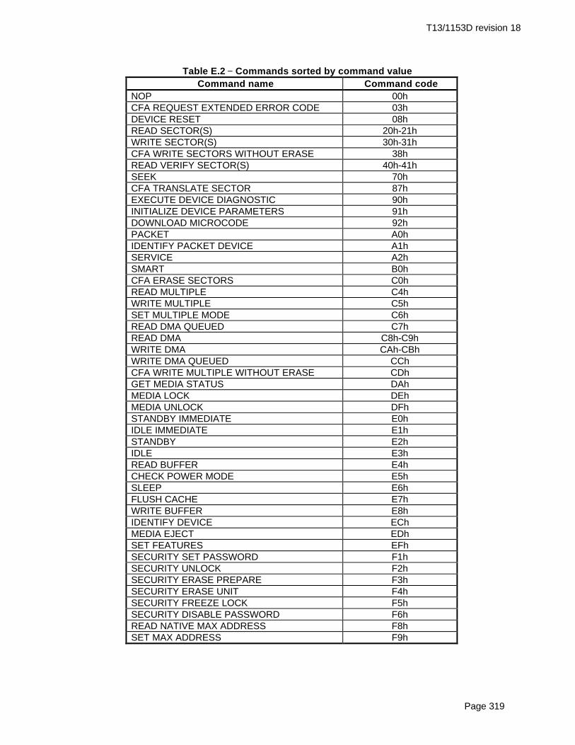
T13/1153D revision 18
Page 319
Table E.2 −− Commands sorted by command valueCommand name Command code
NOP 00hCFA REQUEST EXTENDED ERROR CODE 03hDEVICE RESET 08hREAD SECTOR(S) 20h-21hWRITE SECTOR(S) 30h-31hCFA WRITE SECTORS WITHOUT ERASE 38hREAD VERIFY SECTOR(S) 40h-41hSEEK 70hCFA TRANSLATE SECTOR 87hEXECUTE DEVICE DIAGNOSTIC 90hINITIALIZE DEVICE PARAMETERS 91hDOWNLOAD MICROCODE 92hPACKET A0hIDENTIFY PACKET DEVICE A1hSERVICE A2hSMART B0hCFA ERASE SECTORS C0hREAD MULTIPLE C4hWRITE MULTIPLE C5hSET MULTIPLE MODE C6hREAD DMA QUEUED C7hREAD DMA C8h-C9hWRITE DMA CAh-CBhWRITE DMA QUEUED CChCFA WRITE MULTIPLE WITHOUT ERASE CDhGET MEDIA STATUS DAhMEDIA LOCK DEhMEDIA UNLOCK DFhSTANDBY IMMEDIATE E0hIDLE IMMEDIATE E1hSTANDBY E2hIDLE E3hREAD BUFFER E4hCHECK POWER MODE E5hSLEEP E6hFLUSH CACHE E7hWRITE BUFFER E8hIDENTIFY DEVICE EChMEDIA EJECT EDhSET FEATURES EFhSECURITY SET PASSWORD F1hSECURITY UNLOCK F2hSECURITY ERASE PREPARE F3hSECURITY ERASE UNIT F4hSECURITY FREEZE LOCK F5hSECURITY DISABLE PASSWORD F6hREAD NATIVE MAX ADDRESS F8hSET MAX ADDRESS F9h

T13/1153D revision 18
Page 320
Table E.3 −− Command codes and parametersproto Command typ PKT Command Parameters used
fea code FR SC SN CY DHND CFA ERASE SECTORS O N C0h y y y yND CFA REQUEST EXTENDED ERROR O N 03h DPI CFA TRANSLATE SECTOR O N 87h y y yPO CFA WRITE MULTIPLE W/OUT
ERASEO N CDh y y y y
PO CFA WRITE SECTORS W/OUTERASE
O N 38h y y y y
ND CHECK POWER MODE M M E5h y DDR DEVICE RESET O M 08h DPO DOWNLOAD MICROCODE O N 92h y y y y DDD EXECUTE DEVICE DIAGNOSTIC M M 90h D*ND FLUSH CACHE O O E7h y y y yND GET MEDIA STATUS O O DAh DPI IDENTIFY DEVICE M N ECh DPI IDENTIFY PACKET DEVICE N M A1hND IDLE M O E3h y DND IDLE IMMEDIATE M M E1h DND INITIALIZE DEVICE PARAMETERS M N 91h y yND MEDIA EJECT O O EDh DND MEDIA LOCK O O DEh DND MEDIA UNLOCK O O DFh DND NOP O M 00h DP PACKET N M A0h y y y y DPI READ BUFFER O N E4h D
DM READ DMA M N C8h C9h y y y yDMO READ DMA QUEUED O N C7h y y y y y
PI READ MULTIPLE M N C4h y y y yND READ NATIVE MAX ADDRESS O N F8h DPI READ SECTOR(S) M N 20h 21h y y y yND READ VERIFY SECTOR(S) M N 40h 41h y y y yPO SECURITY DISABLE PASSWORD O O F6h DND SECURITY ERASE PREPARE O O F3h DPO SECURITY ERASE UNIT O O F4h DND SECURITY FREEZE O O F5 DPO SECURITY SET PASSWORD O O F1H DPO SECURITY UNLOCK O O F2h DND SEEK M N 70h y y yP SERVICE N O A2h y y y D
ND SET FEATURES M M EFh y DND SET MAX ADDRESS O N F9h y y y yND SET MULTIPLE MODE M N C6h y DND SLEEP M M E6h DND SMART DISABLE OPERATIONS O O B0h y y DND SMART ENABLE/DISABLE
AUTOSAVEO O B0h y y y D
ND SMART ENABLE OPERATIONS O O B0h y y DND SMART EXECUTE OFF_LINE O O B0h y y DPI SMART READ DATA O O B0h y y DND SMART RETURN STATUS O O B0h y y DND STANDBY M O E2h y DND STANDBY IMMEDIATE M M E0h D
(continued)

T13/1153D revision 18
Page 321
Table E.3 −− Command codes and parameters (concluded)proto Command typ PKT Command Parameters used
fea code FR SC SN CY DHPO WRITE BUFFER O N E8h DDM WRITE DMA M N CAh CBh y y y y
DMO WRITE DMA QUEUED O N CCh y y y y yPO WRITE MULTIPLE M N C5h y y y yPO WRITE SECTOR(S) M N 30h 31h y y y yVS Vendor specific V V 9Ah,C0h-
C3h,8xh,F0h,F7h,FAh-FFh
- Reserved: all remaining codes R RKey:DM = DMA command ND = Non-data command PI = PIO data in commandPO = PIO data out command VS = Vendor specific command O = Optional P=PACKET commandDR = DEVICE RESET protocol DD = EXECUTE DEVICE DIAGNOSTIC protocolDMO = Overlapped/queued DMAtyp=Command type PKT fea=Command type when PACKET Command feature set implementedM = Mandatory R = Reserved N=Not to be used V = Vendor specificimplementationCY = Cylinder registers SC = Sector Count register DH = Device/Head registerSN = Sector Number register FR = Features register (see command descriptions for use)y = the register contains a valid parameter for this command. For the Device/Head register, y means both the deviceand head parameters are used.D = only the device parameter is valid and not the head parameter.d = the device parameter is valid, the usage of the head parameter vendor specific.D* = Addressed to device 0 but both devices execute it.

T13/1153D revision 18
Page 322
Table E.4 −− I/O port functions and selection addresses except PACKET and SERVICE commandsAddresses Functions
CS0- CS1- DA2 DA1 DA0 Read (DIOR-) Write (DIOW-)N N x x x Data bus high impedance Not used
Control block registersN A N x x Data bus high impedance Not usedN A A N x Data bus high impedance Not usedN A A A N Alternate Status Device ControlN A A A A obsolete(see note) Not used
Command block registersA N N N N Data DataA N N N A Error FeaturesA N N A N Sector Count Sector CountA N N A A Sector Number Sector NumberA N A N N Cylinder Low Cylinder LowA N A N A Cylinder High Cylinder HighA N A A N Device/Head Device/HeadA N A A A Status CommandA A x x x Invalid address Invalid address
Key:A = signal asserted, N = signal negated, x = don’t careNOTE − This register is obsolete. It is recommended that a device not respond to a read of thisaddress.
Table E.5 −− I/O port functions and selection addresses for PACKET and SERVICE commandsAddresses Functions
CS0- CS1- DA2 DA1 DA0 Read (DIOR-) Write (DIOW-)N N x x x Data bus high impedance Not used
Control block registersN A N x x Data bus high impedance Not usedN A A N x Data bus high impedance Not usedN A A A N Alternate Status Device ControlN A A A A obsolete(see note) Not used
Command block registersA N N N N Data DataA N N N A Error FeaturesA N N A N Interrupt reasonA N N A AA N A N N Byte count low Byte count lowA N A N A Byte count high Byte count highA N A A N Device select Device selectA N A A A Status CommandA A x x x Invalid address Invalid address
Key:A = signal asserted, N = signal negated, x = don’t careNOTE − This register is obsolete. A device should not respond to a read of this address.

T13/1153D revision 18
Page 323
Annex F(informative)
Command packet format example
Table F.1 is an example of the command packet for most PACKET commands.
Table F.1 −− Command packetByte 7 6 5 4 3 2 1 0
0 Operation code1 reserved reserved2 (MSB)3 Logical block address (if required)45 (LSB)6 reserved
7-8 (MSB) Transfer length (if required) orParameter list length (if required) or
Allocation length (if required) (LSB)9 reserved
10 reserved11 reserved