Embed Size (px)
Citation preview

WIZ830MJ Datasheet (Ver. 1.3)
© 2013 WIZnet Co., Ltd. All Rights Reserved.
For more information, visit our website at www.wiznet.co.kr

WIZ830MJ Datasheet
© Copyright 2008 WIZnet Co., Ltd. All rights reserved
2
TOP
WWIIZZ88
1100MM
JJ
DDaattaa
sshheeee
tt
Document History Information
Revision Data Description
Ver.1.0 June 04, 2008 Release with WIZ830MJ Launching
Ver.1.1 July 29, 2008 Modified dimensions(Symbol B and C).
Ver.1.2 March 4, 2010 Pin number of A[9:0] modified in Chapter 2.3
Ver.1.3 January 28, 2013 Hardware revision(Rev1.1) Changed just partlist at this revision

WIZ830MJ Datasheet
© Copyright 2008 WIZnet Co., Ltd. All rights reserved
3
TOP
WWIIZZ88
1100MM
JJ
DDaattaa
sshheeee
tt
WIZnet’s Online Technical Support
If you have something to ask about WIZnet Products, Write down your question
on Q&A Board in WIZnet website (www.wiznet.co.kr). WIZnet Engineer will give an
answer as soon as possible.

WIZ830MJ Datasheet
© Copyright 2008 WIZnet Co., Ltd. All rights reserved
4
TOP
WWIIZZ88
1100MM
JJ
DDaattaa
sshheeee
tt
Table of Contents
1. Introduction .............................................................................. 5
1.1. Features ................................................................................................... 5
1.2. Block Diagram .......................................................................................... 5
2. Pin Assignments & descriptions ................................................... 6
2.1. Pin Assignments ....................................................................................... 6
2.2. Power & Ground ....................................................................................... 7
2.3. MCU Interfaces ........................................................................................ 7
2.4. Network Indicator LED Signals ................................................................. 8
2.5. Miscellaneous Signals .............................................................................. 8
3. Timing Diagrams ....................................................................... 9
3.1. Reset Timing ............................................................................................ 9
3.2. Register / Memory READ Timing .............................................................. 9
3.3. Register / Memory WRITE Timing .......................................................... 10
4. Dimensions ............................................................................. 11
5. Schematic .............................................................................. 12
6. Partlists .................................................................................. 13
WIZ830MJ Datasheet
© Copyright 2008 WIZnet Co., Ltd. All rights reserved
5
TOP
WWIIZZ88
1100MM
JJ
DDaattaa
sshheeee
tt
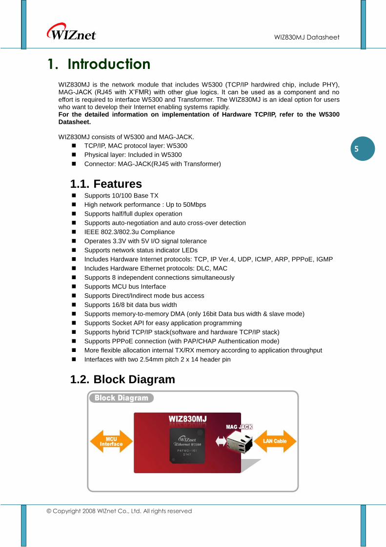
1. Introduction
WIZ830MJ is the network module that includes W5300 (TCP/IP hardwired chip, include PHY), MAG-JACK (RJ45 with X’FMR) with other glue logics. It can be used as a component and no effort is required to interface W5300 and Transformer. The WIZ830MJ is an ideal option for users who want to develop their Internet enabling systems rapidly. For the detailed information on implementation of Hardware TCP/IP, refer to the W5300 Datasheet. WIZ830MJ consists of W5300 and MAG-JACK.
TCP/IP, MAC protocol layer: W5300
Physical layer: Included in W5300
Connector: MAG-JACK(RJ45 with Transformer)
1.1. Features Supports 10/100 Base TX
High network performance : Up to 50Mbps
Supports half/full duplex operation
Supports auto-negotiation and auto cross-over detection
IEEE 802.3/802.3u Compliance
Operates 3.3V with 5V I/O signal tolerance
Supports network status indicator LEDs
Includes Hardware Internet protocols: TCP, IP Ver.4, UDP, ICMP, ARP, PPPoE, IGMP
Includes Hardware Ethernet protocols: DLC, MAC
Supports 8 independent connections simultaneously
Supports MCU bus Interface
Supports Direct/Indirect mode bus access
Supports 16/8 bit data bus width
Supports memory-to-memory DMA (only 16bit Data bus width & slave mode)
Supports Socket API for easy application programming
Supports hybrid TCP/IP stack(software and hardware TCP/IP stack)
Supports PPPoE connection (with PAP/CHAP Authentication mode)
More flexible allocation internal TX/RX memory according to application throughput
Interfaces with two 2.54mm pitch 2 x 14 header pin
1.2. Block Diagram

WIZ830MJ Datasheet
© Copyright 2008 WIZnet Co., Ltd. All rights reserved
6
TOP
WWIIZZ88
1100MM
JJ
DDaattaa
sshheeee
tt
2. Pin Assignments & descriptions
2.1. Pin Assignments

WIZ830MJ Datasheet
© Copyright 2008 WIZnet Co., Ltd. All rights reserved
7
TOP
WWIIZZ88
1100MM
JJ
DDaattaa
sshheeee
tt
I : Input O : Output I/O : Bi-directional Input and output P : Power
2.2. Power & Ground Symbol Type Pin No. Description
VCC P J1:1, J2:1 Power : 3.3 V power supply
GND P J1:18, J2:10, J2:15, J2:16, J2:23, J2:24
Ground
2.3. MCU Interfaces Symbol Type Pin No. Description
A[9:0] I J1:19 ~ J1:28 Address Used as Address[9-0] pin
D[15:8]
I/O
J1:2 ~ J1:9
Data 16 bit-wide high data bus In case of using 8 bit data bus, there are driven as High-Z
D[7:0]
I/O
J1:10 ~ J1:17
Data 16 bit-wide low data bus
/CS I J2:19 Module Select : Active low. /CS of W5300
/RD I J2:20 Read Enable : Active low. /RD of W5300
/WR I J2:21 Write Enable : Active low /WR of W5300
/INT O J2:18
Interrupt : Active low After reception or transmission it indicates that the W5300 requires MCU attention. By writing values to the Interrupt Register(IR) of W5300 the interrupt will be cleared by host. All interrupts can be masked by writing values to the IMR of W5300 (Interrupt Mask Register). For more details refer to the W5300 Datasheet
BIT16EN I J2:2 16/8 bit data bus select. High : 16 bit data bus Low : 8 bit data bus.

WIZ830MJ Datasheet
© Copyright 2008 WIZnet Co., Ltd. All rights reserved
8
TOP
WWIIZZ88
1100MM
JJ
DDaattaa
sshheeee
tt
2.4. Network Indicator LED Signals Symbol Type Pin No. Description
/LINKLED O J2:3 Link LED It indicates the link status of media(10/100M).
/TXLED O J2:4
Transmit activity LED : Transmit Enable It notifies the output of transmit data through TXOP/TXON (Transmit Activity).
/RXLED O J2:5 Receive activity LED : Transmit Data It notifies the input of receive data from RXIP/RXIN (Receive Activity)
/COLLED O J2:6
Collision LED : Transmit Data It notifies when collisions occur. It is valid at half-duplex, and is ignored at full-duplex.
/FDXLED O J2:7
Full duplex LED : Transmit Data It outputs low at the full-duplex and outputs high at the halfduplex according to auto-negotiation or manual configuration of OP_MODE[2:0].
/SPDLED O J2:8
Link speed LED : Transmit Data It is asserted low at the 100Mbps and high at the 10Mbps according to auto-negotiation or manual configuration of OP_MODE[2:0].
/ACTLED O J2:9
Activity LED It notifies the output of transmit data through TXOP/TXON or the input of receive data from RXIP/RXIN.
2.5. Miscellaneous Signals Symbol Type Pin No. Description
/RESET I J2:17
Reset : This pin is active low input to initialize or re-initialize W5300. RESET should be held at least 2us after low assert, and wait for at least 10ms after high de-assert in order for PLL logic to be stable
BRDY[3:0] O J2:11 ~ J2:14
Buffer Ready Indicator BRDYn monitors TX/RX memory status of each socket. For more details refer to the W5300 Datasheet
NC - J2 : 22, J2:25, J2:26, J2:27, J2:28
Not Connect

WIZ830MJ Datasheet
© Copyright 2008 WIZnet Co., Ltd. All rights reserved
9
TOP
WWIIZZ88
1100MM
JJ
DDaattaa
sshheeee
tt
3. Timing Diagrams WIZ830MJ provides following interfaces of W5300. -. Direct/Indirect mode bus access
3.1. Reset Timing
Description Min Max
1 Reset Cycle Time 2 us -
2 PLL Lock-in Time 50us 10 s
3.2. Register / Memory READ Timing
Description Min Max
tADDRs Address Setup Time after /CS and /RD low - 7ns
tADDRh Address Hold Time after /CS and /RD high - -
tCS /CS Low Time 65ns -
tCSn /CS Next Assert Time 28ns -
tRD /RD Low Time 65ns -
tDATAs DATA Setup Time after /RD low 42ns -
tDATAh DATA Hold Time after /RD and /CS high - 7ns
tDATAhe DATA Hold Extension Time after /CS high - 2XPLL_CLK

WIZ830MJ Datasheet
© Copyright 2008 WIZnet Co., Ltd. All rights reserved
10
TOP
WWIIZZ88
1100MM
JJ
DDaattaa
sshheeee
tt
3.3. Register / Memory WRITE Timing
Description Min Max
tADDRs Address Setup Time after /CS and /WR low - 7ns
tADDRh Address Hold Time after /CS or /RD high - -
tCS /CS low Time 50ns -
tCSn /CS next Assert Time 28ns
tWR /WR low Time 50ns
tDATAs Data Setup Time after /WR low 7ns 7ns + 7XPLL_CLK
tDATAf Data Fetch Time 14ns tWR – tDATAs
tDATAh Data Hold Time after /WR high 7ns -

WIZ830MJ Datasheet
© Copyright 2008 WIZnet Co., Ltd. All rights reserved
11
TOP
WWIIZZ88
1100MM
JJ
DDaattaa
sshheeee
tt
4. Dimensions
Symbols Dimensions (mm) Symbols Dimensions (mm)
A 34.00 H 6.50
B 30.48 I 2.54
C 25.40 J 2.54
D 3.00 K 15.90
E 4.00 L 13.50
F 50.00 M 6.00
G 3.30 - -

WIZ830MJ Datasheet
© Copyright 2008 WIZnet Co., Ltd. All rights reserved
12
TOP
WWIIZZ88
1100MM
JJ
DDaattaa
sshheeee
tt
5. Schematic
GH
6
CO
N1
1
Title
Size
Docum
ent N
um
ber
Rev
Date
:S
heet
of
<D
oc>
RE
V.1
.1
WIZ
830M
J
B
11
Monday
, January
28, 2
013
3V
3A
3V
3A
/WR
/CS
/RD
+C
93.3
uF
GN
DA
+C
10
10uF
/16V
+C
11
10uF
/16V
C12
0.1
uF
FB
21uH
1V
8_O
UT
1V
8D
1V
8A
W5300
LQFP100(14X14)
U1
W5300
RS
ET_B
G1
VCC3A32
NC
3
GNDA4
RXIP
5
RXIN
6
VCC1A87
TXO
P8
TXO
N9
GNDA10
VCC1V811
GND12
1V
8O
13
VCC3V314
GND15
GNDA16
VCC1A817
BIT
16E
N18
TE
ST_M
OD
E3
19
TE
ST_M
OD
E2
20
TE
ST_M
OD
E1
21
TE
ST_M
OD
E0
22
OP
_M
OD
E0
23
OP
_M
OD
E1
24
OP
_M
OD
E2
25
VCC3V326
GND27
DA
TA
15
28
DA
TA
14
29
DA
TA
13
30
DA
TA
12
31
DA
TA
11
32
DA
TA
10
33
DA
TA
934
DA
TA
835
VCC1V836
GND37
DA
TA
738
DA
TA
639
DA
TA
540
DA
TA
441
DA
TA
342
DA
TA
243
DA
TA
144
DA
TA
045
VCC3V346
GND47
AD
DR
948
AD
DR
849
AD
DR
750
AD
DR
651
AD
DR
552
AD
DR
453
AD
DR
354
AD
DR
255
AD
DR
156
AD
DR
057
VCC1V858
GND59
/WR
60
/RD
61
/CS
62
VCC3V363
GND64
/INT
65
/RE
SE
T66
BR
DY
067
BR
DY
168
BR
DY
269
BR
DY
370
MII_
RXC
71
VCC1V872
GND73
MII_
RXD
V74
MII_
RXD
075
MII_
RXD
176
MII_
RXD
277
MII_
RXD
378
MII_
CO
L79
/FD
X80
MII_
CR
S81
MII_
TXC
82
VCC3V383
GND84
SP
DLE
D/M
II_TXD
085
FD
XLE
D/M
II_TXD
186
CO
LLE
D/M
II_TXD
287
RXLE
D/M
II_TXD
388
TXLE
D/M
II_TXE
N89
LIN
KLE
D90
OS
C25I
91
VCC1V892GND
93
VCC1V894
XTLN
95
XTLP
96
GND97
NC
98
NC
99
NC
100
/INT
XTLP
XTLN
1V
8_O
UT
R1
12K
(1%
)
/RE
SE
T
3.3
V1V
8D
3V
3A
1V
8A
D15
TXO
P
RS
ET_B
G
D14
TXO
N
RXIN
D13
RXIP
D12
D10
/LIN
KLE
D
D11
D9
/SP
DLE
D
D8
OP
_M
OD
E0
/FD
XLE
D
D7
OP
_M
OD
E1
/CO
LLE
D
OP
_M
OD
E2
/RXLE
D
D5
/TXLE
D
D6
D4
GH
4
CO
N9
123456789
D3
D2
D1
D0
A9
A8
A7
A6
A5
A4
A3
BIT
16E
N
A2
BR
DY
0
A1
BR
DY
1
A0
BR
DY
2B
RD
Y3
XTLP
XTLN
R3
1M
Y1
25M
Hz
C19
15p
C21
15p
1V
8D
C13
0.1
uF
C14
0.1
uF
C15
0.1
uF
C16
0.1
uF
C17
0.1
uF
C18
0.1
uF
R2
300(1
%)
OP
_M
OD
E1
OP
_M
OD
E2
OP
_M
OD
E0
3.3
V
Recommendatory part is 120R@100MHz
C22
0.1
uF
R5
200
TXO
N
R6
49.9
RXIN
C230.1
uF
R4
200
TXO
P
C20
0.1
uF
R7
49.9
U2
BS
-RB
10005
TD
+1
TD
-2
TC
T3
NC
4
NC
5
RC
T6
RD
+7
RD
-8
GR
N+
10
GR
N-
9
YE
L+
12
YE
L-
11
Shie
ld13
Shie
ld14
R8
49.9
RXIP
R9
49.9
FB
4F
B_0805
3.3
V
C1
0.1
uF
C2
0.1
uF
C3
0.1
uF
C4
0.1
uF
C5
0.1
uF
3V
3A
GH
5
CO
N1
1
C6
10uF
/16V
FB
11uH
C8
10uF
/16V
C7
0.1
uF
3.3
V
GN
DA
GN
DA
FB
31uH
GH
3
CO
N9
123456789
GN
DA
A6
A8
D1
D6
D8
D10
D12
D14
A4
A7
A9
D0
D2
D4
/AC
TLE
D/F
DXLE
D/R
XLE
D/L
INK
LE
D
A5
BR
DY
1B
RD
Y3
/WR
/RE
SE
T
/CO
LLE
D/T
XLE
DB
IT16E
N
BR
DY
0B
RD
Y2
/SP
DLE
D
/CS
/INT
J1, J2 : 2.54mm pitch header
3.3
V
/RD
J1
HE
AD
ER
14X2
246810
12
14
16
18
20
22
24
26
28
1357911
13
15
17
19
21
23
25
27
J2
HE
AD
ER
14X2
246810
12
14
16
18
20
22
24
26
28
1357911
13
15
17
19
21
23
25
27
3.3
V
D9
D11
D13
D15
D3
D5
D7
R10
0
R11
0
R13
0
Not mounted
(auto-negotiaton)
/RXLE
D
D1
1S
S181(S
C-5
9) 3
12
/AC
TLE
D
/TXLE
D
R12
4.7
K
3.3
V
A3
A1
A2
A0
/LIN
KLE
D
/AC
TLE
D

WIZ830MJ Datasheet
© Copyright 2008 WIZnet Co., Ltd. All rights reserved
13
TOP
WWIIZZ88
1100MM
JJ
DDaattaa
sshheeee
tt
6. Partlist
Item Q.ty Reference Part Tech. Characteristics Package
1 16 C1,C2,C3,C4,C5,C7, C12,C13,C14,C15,C16, C17,C18,C20,C22,C23
0.1uF 50V-20% Ceramic CASE 0603
2 4 C6,C8,C10,C11 10uF/16V 16Vmin 10% EIA/IECQ 3216
3 1 C9 3.3uF/16V 16Vmin 10% EIA/IECQ 3216
4 2 C19,C21 15pF 50V-20% Ceramic CASE 0603
5 1 D1 1SS181 SC-59
6 3 FB1,FB2,FB3 1uH Chip Ferrite Inductor CASE 0805
7 1 FB4 120 Ohm Ferrite BEAD 120 Ohm /100MHz CASE 0805
8 2 J1,J2 2X14 2.54mm DIP STRAIGHT Header
2 X 14 2.54mm pitch DIP
9 1 R1 12K (1%) 1/10W-1% SMD CASE 0603
10 1 R2 300 (1%) 1/10W-1% SMD CASE 0603
11 1 R3 1M 1/10W-5% SMD CASE 0603
12 2 R4,R5 200 1/10W-5% SMD CASE 0603
13 4 R6,R7,R8,R9 49.9 (1%) 1/10W-1% SMD CASE 0603
14 0 R10,R11,R13 not mounted 1/10W-5% SMD CASE 0603
15 1 R12 4.7K 1/10W-5% SMD CASE 0603
16 1 U1 W5300 WIZnet Hardware TCP/IP LQFP100
17 1 U2 BS-RB10005 Transformer + RJ-45
18 1 Y1 25MHz(SMD) SMD Type, CL=18pF, Industrial
SX-1
19 1 PCB REV1.1 FR4, 1.6T, 4Layer