Embed Size (px)
Citation preview

8/9/2019 Wireless Video Confetrencing System
http://slidepdf.com/reader/full/wireless-video-confetrencing-system 1/43
CONTENT
1. INTRODUCTION
2. DESIGN PRINCIPLE3. CIRCUIT DESCRIPTION
A. Power supply
B. Mother board
C. Led indicator
D. Bi directional Motor driver
E. DC Motor Driver F. Relay Driver
G.DTMF Encoder
H.DTMF Decoder
I. FM Transmitter
J. FM Receiver
K.Audio Amplifier
L. Signal Conditioning Circuit
4. FUTURE EXPANSION
5. CONCLUSION

8/9/2019 Wireless Video Confetrencing System
http://slidepdf.com/reader/full/wireless-video-confetrencing-system 2/43
WIRELESS VIDEO MONITORING SYSTEM
1. INTRODUCTION
The wireless video monitoring system is one of the major equipment used for security
purpose. The security system is not only used in industries but also it is mostly used for private and public security. The security system is one of the major importances in thepresent scenario. A need of all modern industries and public place and private premises
2. DESIGN PRINCIPLE
In this project there is one base station and three wireless monitoring systems, in themonitoring system a wireless camera is installed on rotating tower. The rotating tower isdesigned with a micro controller based stepper motor driver. The stepper motor driver drives the camera base in steps. There are two guide bars placed at the extreme ends

8/9/2019 Wireless Video Confetrencing System
http://slidepdf.com/reader/full/wireless-video-confetrencing-system 3/43
of the camera position. The wireless camera is fixed on the top of the tower, to limit theviewing angle the camera rotation or movement is restricted to a limited angle. Therotating tower rotates with the camera and the camera base is fixed with one logicsignal source, to limit the angle of rotation two feed back signals are taken to the mother board. The micro controller 89c51 programmed to rotate the stepper motor and check
the feed back signal after each step of rotation. When ever the logic signal touches thefeed back point the controller receives the feedback and change the direction of movement. The controller is having two feedback inputs to understand the left and rightextreme positions and on receiving the feedback signal the controller change thedirection of movement of the stepper motor. This way the camera can oscillate with in afixed point from left to right and right to left. There are three wireless stations designedfor monitoring three locations. In this stations there are wireless video cameras aremounted which transmit signal in the AV range of the TV channels.
Base monitoring station
There is another unit called base monitoring station which is designed with an AT 89c51microcontroller. This is basically a sequential switch. Which multiplex the receivedsignal to the TV AV channel. This station is having three receivers and tuned toreceive signals from different video transmitters. The micro controller is designed to

8/9/2019 Wireless Video Confetrencing System
http://slidepdf.com/reader/full/wireless-video-confetrencing-system 4/43
sample the receivers and multiplex to one of the channel of the TV unit used to monitor the three systems. There are three numbers of electromagnetic relays which is operatedwith time slot. In the relay array only one relay is remained closed for a given timeperiod and others are remained open. This sequential switching allot the time slat to thereceiver for viewing the video.
3. CIRCUIT DESCRIPTION
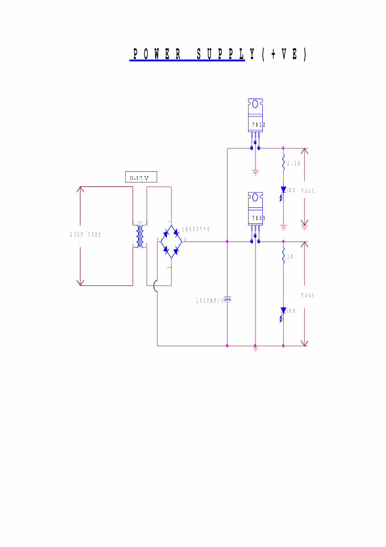
A. POWER SUPPLY
Circuit connection:- In this we are using Transformer(0-12)v,1Amp, IC 7805 & 7812,diodes IN 4007,LED & resistors.
Here 230V,50 Hz ac signal is given as input to the primary of the transformer and thesecondary of the transformer is given to the bridge rectification diode. The o/p of thediode is given as i/p to the IC regulator (7805 &7812) through capacitor (1000mf/35v).The o/p of the IC regulator is given to the LED through resistors.Circuit Explanations:- When ac signal is given to the primary of the transformer, dueto the magnetic effect of the coil magnetic flux is induced in the coil(primary) andtransfer to the secondary coil of the transformer due to the transformer action.”Transformer is an electromechanical static device which transformer electrical energyfrom one coil to another without changing its frequency”. Here the diodes are connectedin a bridge fashion. The secondary coil of the transformer is given to the bridge circuitfor rectification purposes.

8/9/2019 Wireless Video Confetrencing System
http://slidepdf.com/reader/full/wireless-video-confetrencing-system 5/43
During the +ve cycle of the ac signal the diodes D2 & D4 conduct due to the forwardbias of the diodes and diodes D1 & D3 does not conduct due to the reversed bias of thediodes. Similarly during the –ve cycle of the ac signal the diodes D1 & D3 conduct dueto the forward bias of the diodes and the diodes D2 & D4 does not conduct due toreversed bias of the diodes. The output of the bridge rectifier is not a power dc along
with rippled ac is also present. To overcome this effect, a capacitor is connected to theo/p of the diodes (D2 & D3). Which removes the unwanted ac signal and thus a pure dcis obtained. Here we need a fixed voltage, that’s for we are using IC regulators (7805 &7812).”Voltage regulation is a circuit that supplies a constant voltage regardless of changes in load current.” This IC’s are designed as fixed voltage regulators and withadequate heat sinking can deliver output current in excess of 1A. The o/p of the bridgerectifier is given as input to the IC regulator through capacitor with respect to GND andthus a fixed o/p is obtained. The o/p of the IC regulator (7805 & 7812) is given to theLED for indication purpose through resistor. Due to the forward bias of the LED, the
LED glows ON state, and the o/p are obtained from the pin no-3.
B. MOTHERBOARD
Introduction
Despite it’s relatively old age, the 89C51 is one of the most popular Microcontroller inuse today. Many derivatives Microcontroller have since been developed that are basedon--and compatible with--the 8051. Thus, the ability to program an 89C51 is animportant skill for anyone who plans to develop products that will take advantage of Microcontroller.
Many web pages, books, and tools are available for the 89C51 developer.
The 89C51 has three very general types of memory. To effectively program the 8051 itis necessary to have a basic understanding of these memory types.
The memory types are illustrated in the following graphic. They are: On-Chip Memory,External Code Memory, and External RAM.

8/9/2019 Wireless Video Confetrencing System
http://slidepdf.com/reader/full/wireless-video-confetrencing-system 6/43
On-Chip Memory refers to any memory (Code, RAM, or other) that physically exists onthe Microcontroller itself. On-chip memory can be of several types, but we'll get into thatshortly.
External Code Memory is code (or program) memory that resides off-chip. This is oftenin the form of an external EPROM.
External RAM is RAM memory that resides off-chip. This is often in the form of standard static RAM or flash RAM.
Code Memory
Code memory is the memory that holds the actual 8051 program that is to be run. Thismemory is limited to 64K and comes in many shapes and sizes: Code memory may befound on-chip, either burned into the Microcontroller as ROM or EPROM. Code mayalso be stored completely off-chip in an external ROM or, more commonly, an externalEPROM. Flash RAM is also another popular method of storing a program. Variouscombinations of these memory types may also be used--that is to say, it is possible tohave 4K of code memory on-chip and 64k of code memory off-chip in an EPROM.
When the program is stored on-chip the 64K maximum is often reduced to 4k, 8k, or 16k. This varies depending on the version of the chip that is being used. Each versionoffers specific capabilities and one of the distinguishing factors from chip to chip is howmuch ROM/EPROM space the chip has. However, code memory is most commonlyimplemented as off-chip EPROM. This is especially true in low-cost developmentsystems and in systems developed by students.

8/9/2019 Wireless Video Confetrencing System
http://slidepdf.com/reader/full/wireless-video-confetrencing-system 7/43
Programming Tip: Since code memory is restricted to 64K, 89C51 programs arelimited to 64K. Some assemblers and compilers offer ways to get around this limit whenused with specially wired hardware. However, without such special compilers andhardware, programs are limited to 64K.
External RAM
As an obvious opposite of Internal RAM , the 89C51 also supports what is calledExternal RAM .
As the name suggests, External RAM is any random access memory which is found off-
chip. Since the memory is off-chip it is not as flexible in terms of accessing, and is alsoslower. For example, to increment an Internal RAM location by 1 requires only 1instruction and 1 instruction cycle. To increment a 1-byte value stored in External RAMrequires 4 instructions and 7 instruction cycles. In this case, external memory is 7 times
slower!
What External RAM loses in speed and flexibility it gains in quantity. While Internal RAMis limited to 128 bytes (256 bytes with an 8052), the 8051 supports External RAM up to64K.
Programming Tip: The 8051 may only address 64k of RAM. To expand RAM beyondthis limit requires programming and hardware tricks. You may have to do this "by hand"since many compilers and assemblers, while providing support for programs in excessof 64k, do not support more than 64k of RAM. This is rather strange since it has beenmy experience that programs can usually fit in 64k but often RAM is what is lacking.Thus if you need more than 64k of RAM, check to see if your compiler supports it but if it doesn't, be prepared to do it by hand.
On-Chip Memory
As mentioned at the beginning of this chapter, the 89C51 includes a certain amount of on-chip memory. On-chip memory is really one of two types: Internal RAM and SpecialFunction Register (SFR) memory. The layout of the 89C51's internal memory is
presented in the following memory map:

8/9/2019 Wireless Video Confetrencing System
http://slidepdf.com/reader/full/wireless-video-confetrencing-system 8/43
As is illustrated in this map, the 8051 has a bank of 128 bytes of Internal RAM . ThisInternal RAM is found on-chip on the 8051 so it is the fastest RAM available, and it isalso the most flexible in terms of reading, writing, and modifying it’s contents. InternalRAM is volatile, so when the 8051 is reset this memory is cleared.
The 128 bytes of internal ram is subdivided as shown on the memory map. The first 8bytes (00h - 07h) are "register bank 0". By manipulating certain SFRs, a program maychoose to use register banks 1, 2, or 3. These alternative register banks are located ininternal RAM in addresses 08h through 1Fh. We'll discuss "register banks" more in alater chapter. For now it is sufficient to know that they "live" and are part of internalRAM.
Bit Memory also lives and is part of internal RAM. We'll talk more about bit memory veryshortly, but for now just keep in mind that bit memory actually resides in internal RAM,from addresses 20h through 2Fh.
The 80 bytes remaining of Internal RAM, from addresses 30h through 7Fh, may beused by user variables that need to be accessed frequently or at high-speed. This area
is also utilized by the Microcontroller as a storage area for the operating stack . This factseverely limits the 8051’s stack since, as illustrated in the memory map, the areareserved for the stack is only 80 bytes--and usually it is less since this 80 bytes has tobe shared between the stack and user variables.

8/9/2019 Wireless Video Confetrencing System
http://slidepdf.com/reader/full/wireless-video-confetrencing-system 9/43
SFR Descriptions
There are different special function registers (SFR) designed in side the 89C51 microcontroller. In this micro controller all the input , output ports, timers interrupts arecontrolled by the SFRs. The SFR functionalities are as follows.
This section will endeavor to quickly overview each of the standard SFRs found in theabove SFR chart map. It is not the intention of this section to fully explain thefunctionality of each SFR--this information will be covered in separate chapters of thetutorial. This section is to just give you a general idea of what each SFR does.
P0 (Port 0, Address 80h, Bit-Addressable): This is input/output port 0. Each bit of thisSFR corresponds to one of the pins on the Microcontroller. For example, bit 0 of port 0is pin P0.0, bit 7 is pin P0.7. Writing a value of 1 to a bit of this SFR will send a highlevel on the corresponding I/O pin whereas a value of 0 will bring it to a low level.
Programming Tip: While the 8051 has four I/O port (P0, P1, P2, and P3), if your hardware uses external RAM or external code memory (i.e., your program is stored inan external ROM or EPROM chip or if you are using external RAM chips) you may notuse P0 or P2. This is because the 8051 uses ports P0 and P2 to address the externalmemory. Thus if you are using external RAM or code memory you may only use portsP1 and P3 for your own use.
SP (Stack Pointer, Address 81h): This is the stack pointer of the Microcontroller. This
SFR indicates where the next value to be taken from the stack will be read from inInternal RAM. If you push a value onto the stack, the value will be written to the addressof SP + 1. That is to say, if SP holds the value 07h, a PUSH instruction will push thevalue onto the stack at address 08h. This SFR is modified by all instructions whichmodify the stack, such as PUSH, POP, LCALL, RET, RETI, and whenever interrupts areprovoked by the Microcontroller.Programming Tip: The SP SFR, on startup, is initialized to 07h. This means the stackwill start at 08h and start expanding upward in internal RAM. Since alternate register banks 1, 2, and 3 as well as the user bit variables occupy internal RAM from addresses08h through 2Fh, it is necessary to initialize SP in your program to some other value if
you will be using the alternate register banks and/or bit memory. It's not a bad idea toinitialize SP to 2Fh as the first instruction of every one of your programs unless you are100% sure you will not be using the register banks and bit variables.
DPL/DPH (Data Pointer Low/High, Addresses 82h/83h): The SFRs DPL and DPHwork together to represent a 16-bit value called the Data Pointer . The data pointer isused in operations regarding external RAM and some instructions involving code

8/9/2019 Wireless Video Confetrencing System
http://slidepdf.com/reader/full/wireless-video-confetrencing-system 10/43
memory. Since it is an unsigned two-byte integer value, it can represent values from0000h to FFFFh (0 through 65,535 decimal).Programming Tip: DPTR is really DPH and DPL taken together as a 16-bit value. Inreality, you almost always have to deal with DPTR one byte at a time. For example, topush DPTR onto the stack you must first push DPL and then DPH. You can't simply
plush DPTR onto the stack. Additionally, there is an instruction to "increment DPTR."When you execute this instruction, the two bytes are operated upon as a 16-bit value.However, there is no instruction that decrements DPTR. If you wish to decrement thevalue of DPTR, you must write your own code to do so.
PCON (Power Control, Addresses 87h): The Power Control SFR is used to controlthe 8051's power control modes. Certain operation modes of the 8051 allow the 8051 togo into a type of "sleep" mode which requires much less power. These modes of operation are controlled through PCON. Additionally, one of the bits in PCON is used to
double the effective baud rate of the 8051's serial port.
TCON (Timer Control, Addresses 88h, Bit-Addressable): The Timer Control SFR isused to configure and modify the way in which the 8051's two timers operate. This SFRcontrols whether each of the two timers is running or stopped and contains a flag toindicate that each timer has overflowed. Additionally, some non-timer related bits arelocated in the TCON SFR. These bits are used to configure the way in which theexternal interrupts are activated and also contain the external interrupt flags which areset when an external interrupt has occurred.
TMOD (Timer Mode, Addresses 89h): The Timer Mode SFR is used to configure themode of operation of each of the two timers. Using this SFR your program mayconfigure each timer to be a 16-bit timer, an 8-bit auto reload timer, a 13-bit timer, or two separate timers. Additionally, you may configure the timers to only count when anexternal pin is activated or to count "events" that are indicated on an external pin.
TL0/TH0 (Timer 0 Low/High, Addresses 8Ah/8Ch): These two SFRs, taken together,represent timer 0. Their exact behavior depends on how the timer is configured in theTMOD SFR; however, these timers always count up. What is configurable is how andwhen they increment in value.
TL1/TH1 (Timer 1 Low/High, Addresses 8Bh/8Dh): These two SFRs, taken together,represent timer 1. Their exact behavior depends on how the timer is configured in theTMOD SFR; however, these timers always count up. What is configurable is how andwhen they increment in value.

8/9/2019 Wireless Video Confetrencing System
http://slidepdf.com/reader/full/wireless-video-confetrencing-system 11/43
P1 (Port 1, Address 90h, Bit-Addressable): This is input/output port 1. Each bit of thisSFR corresponds to one of the pins on the Microcontroller. For example, bit 0 of port 1is pin P1.0, bit 7 is pin P1.7. Writing a value of 1 to a bit of this SFR will send a highlevel on the corresponding I/O pin whereas a value of 0 will bring it to a low level.
SCON (Serial Control, Addresses 98h, Bit-Addressable): The Serial Control SFR isused to configure the behavior of the 8051's on-board serial port. This SFR controls thebaud rate of the serial port, whether the serial port is activated to receive data, and alsocontains flags that are set when a byte is successfully sent or received.
Programming Tip: To use the 8051's on-board serial port, it is generally necessary toinitialize the following SFRs: SCON, TCON, and TMOD. This is because SCON controlsthe serial port. However, in most cases the program will wish to use one of the timers toestablish the serial port's baud rate. In this case, it is necessary to configure timer 1 byinitializing TCON and TMOD.
SBUF (Serial Control, Addresses 99h): The Serial Buffer SFR is used to send andreceive data via the on-board serial port. Any value written to SBUF will be sent out theserial port's TXD pin. Likewise, any value which the 8051 receives via the serial port'sRXD pin will be delivered to the user program via SBUF. In other words, SBUF servesas the output port when written to and as an input port when read from.
P2 (Port 2, Address A0h, Bit-Addressable): This is input/output port 2. Each bit of thisSFR corresponds to one of the pins on the Microcontroller. For example, bit 0 of port 2
is pin P2.0, bit 7 is pin P2.7. Writing a value of 1 to a bit of this SFR will send a highlevel on the corresponding I/O pin whereas a value of 0 will bring it to a low level.
Programming Tip: While the 8051 has four I/O port (P0, P1, P2, and P3), if your hardware uses external RAM or external code memory (i.e., your program is stored inan external ROM or EPROM chip or if you are using external RAM chips) you may notuse P0 or P2. This is because the 8051 uses ports P0 and P2 to address the externalmemory. Thus if you are using external RAM or code memory you may only use portsP1 and P3 for your own use.
IE (Interrupt Enable, Addresses A8h): The Interrupt Enable SFR is used to enableand disable specific interrupts. The low 7 bits of the SFR are used to enable/disable thespecific interrupts, where as the highest bit is used to enable or disable ALL interrupts.Thus, if the high bit of IE is 0 all interrupts are disabled regardless of whether anindividual interrupt is enabled by setting a lower bit.

8/9/2019 Wireless Video Confetrencing System
http://slidepdf.com/reader/full/wireless-video-confetrencing-system 12/43
P3 (Port 3, Address B0h, Bit-Addressable): This is input/output port 3. Each bit of thisSFR corresponds to one of the pins on the Microcontroller. For example, bit 0 of port 3is pin P3.0, bit 7 is pin P3.7. Writing a value of 1 to a bit of this SFR will send a highlevel on the corresponding I/O pin whereas a value of 0 will bring it to a low level.
The Microcontroller design consist of two parts1) Hardware.2) Software.
HARDWARE: The controller operates on +5 V dc, so the regulated +v 5 v issupplied to pin no . 40 and ground at pin no. 20. The controller is used here need notrequired to handle high frequency signals, so as 4 MHz crystal is used for operating theprocessor. The pin no. 9 is supplied with a +5V dc through a push switch. To reset theprocessor .As prepare codes are store in the internal flash memory the pin no. 31 isconnected to + Vcc.
C. LED INDICATOR
The indicator section consists of a light emitting diode and its driver circuit is designedon the basis of current required to glow the light emitting diode. Here the driver circuit isrequired for the following functionality.
1) The Microcontroller cannot provide adequate current for glowing the LED. TheLED’s requires a current between 10mA to 20mA of current to glow.
2) The driver circuit provides current to the load from a separate source, so the loadcurrent used not pass through the Microcontroller.
3) The driver circuit activates the load on receipt of a logic signal from theMicrocontroller and of the load in the absence of the signal as he currentrequirement Is very less to glow a LED a single stage driver is sufficient to drivethe load. The driver circuit is nothing other than a perfect a transistor switch. Thedriver transistor goes in to saturation on receipt of base signal and drives intocut-off region, in absence of base signal.The driver designs around a BC548/BC547 transistor and designed for a workingvoltage of +5 V dc and 10mA current.
Rc= Vcc-VCEsat = 5-0.2VIC 10mA
= 4.8KΩ
Ib=Ic/β =10mA/200=5x10-5 A=0.5x10⁻⁶A
=0.5µ A
As per the design a 0.5µ A current is sufficient to trigger the driver circuit. As this
current is very small and to avoid mistriggering a base current of 100µ A is assumed
VB-IBRB-VBE=0 ⇒ IBRB = 5-0.7

8/9/2019 Wireless Video Confetrencing System
http://slidepdf.com/reader/full/wireless-video-confetrencing-system 13/43
RB = 5-0.7V/100µ A = 4.3/100 MΩ
= 0.043x10⁻⁶Ω = 43KΩOn approximation 68K is connected by calculating back
IB = 4.3/68K = 60≅ 70µ A
Which is adequate to avoid mis-triggering level also this amount of current can bedrawn from the Microcontroller without any problem.The indicator section consists of 8 no of driver with 8 no of LED as indicator load. The circuit diagram is enclosed .
Whenever there is a fault in any of the condition (parameter) it indicates a highoutput at the Microcontroller, which is given to the base of the driver transistor (BC547/BC548) with a base resistance (68k/56k) & thus transistor r comes to saturation condition i.e. ON condition, thus the emitter current flows to thecollector of the transistor at which the LED is connected through a current limitingresistor (330E/470E) thus the LED gets forward biased which turns ON the LED itindicates the channels fault .
D) BIDIRECTIONAL MOTOR DRIVER
ELECTRO MAGNETIC RELAY
These are very much reliable devices and widely used on field. The operatingfrequency of these devices are minimum 10-20ms.That is 50Hz – 100Hz.The relaywhich is used here can care 7mA currents continuously. The electromagnetic relayoperates on the principle magnetism. When the base voltage appears at the relay driver section, the driver transistor will be driver transistor will be driven into saturation andallow to flow current in the coil of the relay, Which in turn create a magnetic field and themagnetic force produced due to that will act against the spring tension and close thecontact coil. Whenever the base voltage is withdrawn the transistor goes to cutoff .Sono current flow in the coil of the relay. Hence the magnetic field disappears so thecontact point breaks automatically due to spring tension. Those contact points areisolated from the low voltage supply, so a high voltage switching is possible by the helpof electromagnetic relays.The electromagnetic relays normally having 2 contact points. Named as normally closes
(NC) NO normally open (NO). Normally closed points will so a short CKT path when therelay is off. Normally open points will so a short CKT path when the relay is energized.Circuit operation:
Here the relay drivers are used for the controlling of the car due to the right and leftobstacle. At normal condition, the output of the AND & OR gate are LOW due to whichboth of the relays is in OFF state or de-energized means the contactor point i.e. COM &

8/9/2019 Wireless Video Confetrencing System
http://slidepdf.com/reader/full/wireless-video-confetrencing-system 14/43
NC is in that position means is in same potential. That output signal is given to the bi-directional dc motor driver through a NOT gate, means at the normal condition both of the relay driver is in OFF condition, thus the output of the NOT gate are normally HIGHwhich drives the both of the DC motor is in forward direction through Bi-directional DCmotor driver. The operation of the relay driver is given below:
This application is in some ways a continuation of he discussion introduced for diodeshow the effects of inductive kick can be minimized through proper design. In the belowfigure (a), a transistor is used to established the current necessary to energize the relayin the collector circuit. With no input at the base of the transistor, the base current,collector current, and the coil current are essentially 0A, and the relay sits in theunexercised state (normally open, NO).However when a positive pulse is applied to the base, the transistor turns ON,establishing sufficient current through the coil of the electromagnet to close the relay.Problem can be now develop when the signal is removed from the base to turn OFF the
transistor and de-energized the relay. Ideally, the current through he coil and thetransistor will quickly drop to zero, the arm of the relay will be released, and the relaywill simply remain dormant until the next “ON” signal. However we know from our basiccircuit courses that the current through the coil cannot change instantaneously, and infact the more quickly changes, greater the induced voltage across the coil as definedby,V L = L (di L / dt).
In this case, the rapid changing current through the coil will develop a large voltageacross the coil with the polarity shown in figure (a), which will appear directly across the
output of the transistor. The chances are likely that its magnitude will exceeds themaximum ratings of the transistor, and the semiconductor device will be permanentlydamaged. The voltage across the coil will not remain at its highest switching level butwill oscillate as shown until its level drops to zero as the system settles down.The destructive action can be subdued by placing a diode across the coil as shown inbelow figure (b). During the “ON” state of the transistor, the diode is back biased: it sitslike an open circuit and does not affect the thing. However, when the transistor turns“OFF”, the voltage across the coil will reverse and will forward biased the diode, placingthe diode in its “ON” state. The current through the inductor established during “ON”state of the transistor can then continue to flow through the diode, eliminating thesevere change in current level. Because the inductive current is switched to diodealmost instantaneously after the “OFF” state is established, the diode must have acurrent rating to match the current through the inductor and the transistor when is in“ON” state. Eventually, because of the resistive elements in the loop, including theresistance of the coil windings and the diode, the high frequency (quickly oscillating)variation in voltage level across the coil will decay to zero and the system will settledown.

8/9/2019 Wireless Video Confetrencing System
http://slidepdf.com/reader/full/wireless-video-confetrencing-system 15/43
V c c = + 1 2 v
B C 5 4 7
B C 5 4 7
1 . 5 k
V c c = + 1 2 v
1
0
u
F
R
E
L
A
Y
+
-
1
N
4
0
0
7
R
E
L
A
Y
1 . 5 k
D C M O T O R D R I
M
V c c = + 1 2 v
1
0
u
F
1
N
4
0
0
7
E. DC Motor driver

8/9/2019 Wireless Video Confetrencing System
http://slidepdf.com/reader/full/wireless-video-confetrencing-system 16/43
The D.C. Motor used in this project operates at 12 volt and carries approximately400mA of current. The motor driver is designed to inter face the motor with TTL logic.The TTL output is +12volt and can maximum give a current of 25µA. The driver stagechanges the current and voltage level suitably to drive the motor. The driver stage notonly drives the motor but also helps to control the direction of rotation. As the output
current (Ic) is large the driver section requires a Darlington pair to switch the load. TheDarlington pair I.C. TIP 122 is used here for designing. Here the driver stage isconfigured as a Emitter Follower (C.C) configuration for impedance matching and theoutput is given to the Dc motor to drive the motor smoothly.
F ) RELAY DRIVER
The relay driver is design by using a BC547 transistor .The relay used here havingthe specification as follows
Coil resistance =400ohm Coil voltage=12Vdc
Contact capacity=230V, 7A
The above specification indicates that the coil requires 12V dc and 200mA current dc.The Microcontroller can’t supply more then 10mA current. So driver section is verymuch required. BC547 has a typical current gain of 200 and maximum current capacity
of 1A. So a typical base current of 200 µ A can trigger to on the relay.
ELECTRO MAGNETIC RELAY
These are vary much reliable devices and widely used on field. The operatingfrequency of these devices are minimum 10-20ms.That is 50Hz – 100Hz.The relaywhich is used here can care 25mA currents continuously. The electromagnetic relayoperates on the principle magnetism. When the base voltage appears at the relaydriver section, the driver transistor will be driver transistor will be driven into saturationand allow to flow current in the coil of the relay, Which in turn create a magnetic fieldand the magnetic force produced due to that will act against the spring tension andclose the contact coil. Whenever the base voltage is withdrawn the transistor goes to
cutoff .So no current flow in the coil of the relay. Hence the magnetic field disappearsso the contact point breaks automatically due to spring tension. Those contact pointsare isolated from the low voltage supply, so a high voltage switching is possible by thehelp of electromagnetic relays.The electromagnetic relays normally having 2 contact points. Named as normallycloses (NC), normally open (NO). Normally closed points will so a short CKT path

8/9/2019 Wireless Video Confetrencing System
http://slidepdf.com/reader/full/wireless-video-confetrencing-system 17/43
when the relay is off. Normally open points will so a short CKT path when the relay isenergized.
1 0 u F
R E L A Y D R I V E R
1 . 5 K
B C 5 4 7
D A T A
I N P U T
I N 4 0 0 7
R E L A Y S P
3
5
4
1
2
V C C
G) DTMF ENCODER
Introduction to DTMF
DTMF means: Dual Tone Multi-Frequency, There is no base band multiplexing done on
DTMF signals. The signal generated by a DTMF encoder is a direct algebraicsummation, in real time, of the amplitudes of two sine (cosine) waves of differentfrequencies. i.e. pressing '1' will send a tone made by adding 1209 Hz and 697 Hz tothe other end of the line.
What frequencies used for touch tones numbers

8/9/2019 Wireless Video Confetrencing System
http://slidepdf.com/reader/full/wireless-video-confetrencing-system 18/43
The touch tone system uses pairs of tones to represent the various keys. There is a"low tone" and a "high tone" associated with each button (0 through 9, plus * (star) and#. The low tones vary according to what horizontal row the tone button is in, while thehigh tones correspond to the vertical column of the tone button.
The tones and assignments are as follows:
Matrix Key Board Form:
or:
1209 Hz 1336 Hz 1477 Hz 1633 Hz
ABC DEF697 Hz 1 2 3 A
GHI JKL MNO770 Hz 4 5 6 B
PRS TUV WXY852 Hz 7 8 9 C

8/9/2019 Wireless Video Confetrencing System
http://slidepdf.com/reader/full/wireless-video-confetrencing-system 19/43
oper 941 Hz * 0 # D
Algebric/ Mathematical Form
1 697+12092 697+13363 697+14774 770+12095 770+13366 770+14777 852+12098 852+13369 852+14770 941+1336* 941+1209
# 941+1477A 697+1633B 770+1633C 852+1633D 941+1633
When the 4 button is pressed, the 770 Hz and 1209 Hz tones are sent together from theDTMF encoder. The DTMF decoder decodes the tone and generates the equivalent of the key number at the output.
The tone frequencies were designed to avoid harmonics and other problems that could
arise when two tones are sent and received. Accurate transmission from the encoder and accurate decoding on the decoder is important. They may sound rather musicalwhen dialed (and representations of many popular tunes are possible).
The tones should all be +/- 1.5% of nominal. The high frequency tone should be at leastas loud, and preferably louder than the low frequency. It may be as much as 4 dblouder. This factor is referred to as "twist." If a Touchtone signal has +3db of twist, thenthe high frequency is 3 db louder than the low frequency. Negative twist is when the lowfrequency is louder.
The A, B, C and D touch tone keys and their function:
These are extensions to the standard touch-tones (0-9, *, #) which originated with theU.S. military's Autovon phone network. The original names of these keys were FO(Flash Override), F (Flash), I (Immediate), and P (Priority) which represented prioritylevels that could establish a phone connection with varying degrees of immediacy,killing other conversations on the network if necessary with FO being the greatest

8/9/2019 Wireless Video Confetrencing System
http://slidepdf.com/reader/full/wireless-video-confetrencing-system 20/43
priority, down to P being of lesser priority. The tones are more commonly referred to asthe A, B, C and D tones respectively, and all use a 1633 Hz as their high tone.
Nowadays, these keys/tones are mainly used in special applications such as amateur radio repeaters for their signalling/control. Modems and touch tone circuits tend to
include the A, B, C and D tones as well. These tones have not been used for generalpublic service, and it would take years before these tones could be used in such thingsas customer information lines; such services would have to be compatible with theexisting 12-button touch tone sets in any case.
In DTMF, the tone '8' is represented with the sum of 852 Hz and 1477 Hz sinusoids. Weunderstand that the energy of the sinusoids present in the generated tone shouldexceed the energy present at any other frequencies by 30dB. Also, notice that theDTMF frequencies are effectively divided into two subsets. One contains the lower four frequencies, and the other contains the upper four. Each DTMF tone is defined by thepresence of exactly one of the frequencies from each of those subsets.CCITT DTMF RecommendationsFrequency Tolerance: Operation: <= 1.5%
Non-Operation: >= 3.5%Signal Duration: Operation: 40ms max
Non-Operation: 23ms minSignal Interruption: 10ms maxTwist: Normal: 8db max
Reverse: 4db max
We assume these recommendations are among the most noteworthy, mostly because
they are mentioned in our sources, especially
It took us a while to decide what the each of the recommendations mean. Anyfrequency within 1.5% of the DTMF frequency should be detected. Frequencies with3.5% error should never be detected. Inside the 1.5% - 3.5% range is a don't care.DTMF signals lasting 40ms should always be detected. Signals less than 23ms shouldnever be detected. Inside the 23ms-40ms range is a don't care. DTMF signals that areinterrupted for 10ms or less should not detect two separate signals. Twist is caused bya non-uniform power loss across the frequency spectrum. Normal twist is when lowfrequency power is greater than high frequency. Reverse twist is obviously the reverse
condition. The detector must be reject 8db and 4db for normal and reverse twistrespectively.
We have not found any DSP DTMF implementations that are able to meet thesespecifications. Some algorithms come much closer than others, but none meet thespecifications completely. We are attempting to improve upon the current DTMFimplementations and hopefully meet most (if not all) of the CCITT recommendations.

8/9/2019 Wireless Video Confetrencing System
http://slidepdf.com/reader/full/wireless-video-confetrencing-system 21/43
Encoding DTMF:
There are many ways to generate DTMF tone. Using oscillator and filter array is one of the method also this can be designed by using lookup table in the digital method.The Integrated IC version is having one key board section, on receiving proper rowcolumn section the tone generator section generator generates DTMF tone output.
Encoder IC Operation:
The DTMF encoder IC UM91214B/ UM91215B based circuit generates DTMFfrequencies as per the key pressed in the keyboard connected to the ROW andCOULMN of the IC. This IC requires 3 volts for its operation. This is provided by a
simple zener diode voltage regulator, which converts 9 volts into 3 volts for use by thisIC. For its time base, it requires a quartz crystal of 3.58 MHz. The Encoder IC Pins 1and 2 are used as chip select and DTMF mode select pins respectively. When the rowand column pins (12 and 15) are shorted to each other, DTMF tones corresponding todigit 1 are output from its pin 7.

8/9/2019 Wireless Video Confetrencing System
http://slidepdf.com/reader/full/wireless-video-confetrencing-system 22/43
H) DTMF DECODER
Features:
• Low Power Consumption• Adjustable Acquisition and Release Times• Central Office Quality and Performance
• Power-down and Inhibit Modes• Inexpensive 3.58 MHz Time Base• Single 5 Volt Power Supply• Dial Tone Suppression
Applications:
• Telephone switch equipment• Remote data entry• Paging systems• Personal computers• Credit card systems
Description:

8/9/2019 Wireless Video Confetrencing System
http://slidepdf.com/reader/full/wireless-video-confetrencing-system 23/43
The M-8870 is a full DTMF Receiver that integrates both bandsplit filter and decoder functions into a single 18-pin DIP or SOIC package. Manufactured using CMOS processtechnology, the M-8870 offers low power consumption (35 mW max) and precise datahandling. Its filter section uses switched capacitor technology for both the high and lowgroup filters and for dial tone rejection. Its decoder uses digital counting techniques to
detect and decode all 16 DTMF tone pairs into a 4-bit code. External component countis minimized by provision of an on-chip differential input amplifier, clock generator, andlatched tri-state interface bus. Minimal external components required include a low-cost3.579545 MHz color burst crystal, a timing resistor, and a timing capacitor.The M-8870-02 provides a “power-down” option which, when enabled, drops consumption to lessthan 0.5 mW. The CM-8870 - 02 can also inhibit the decoding of fourth column digits .
Functional Description
CM-8870 operating functions (see block diagram on page 1) include a band split filter that separates the high and low tones of the received pair, and a digital decoder thatverifies both the frequency and duration of the received tones before passing theresulting 4-bit code to the output bus.
Filter
The low and high group tones are separated by applying the dual-tone signal to theinputs of two 6th order switched capacitor bandpass filters with bandwidths thatcorrespond to the bands enclosing the low and high group tones. The filter also
incorporates notches at 350 and 440 Hz, providing excellent dial tone rejection. Eachfilter output is followed by a single-order switched capacitor section that smoothes thesignals prior to limiting. Signal limiting is performed by high gain comparators providedwith hysteresis to prevent detection of unwanted low-level signals and noise. Thecomparator outputs provide full-rail logic swings at the frequencies of the incomingtones.
Decoder
The M-8870 decoder uses a digital counting technique to determine the frequencies of the limited tones and to verify that they correspond to standard DTMF frequencies. Acomplex averaging algorithm is used to protect against tone simulation by extraneoussignals (such as voice) while tolerating small frequency variations. The algorithmensures an optimum combination of immunity to talkoff and tolerance to interferingsignals (third tones) and noise. When the detector recognizes the simultaneous

8/9/2019 Wireless Video Confetrencing System
http://slidepdf.com/reader/full/wireless-video-confetrencing-system 24/43
presence of two valid tones (known as signal condition), it raises the Early Steering flag(ESt). Any subsequent loss of signal condition will cause ESt to fall.
Steering Circuit
Before a decoded tone pair is registered, the receiver checks for a valid signal duration(referred to as character- recognition-condition). This check is performed by an externalRC time constant driven by ESt. A logic high on ESt causes VC (see block diagram onpage 1) to rise as the capacitor discharges. Provided that signal condition is maintained(ESt remains high) for the validation period (tGTF), VC reaches the threshold (VTSt) of the steering logic to register the tone pair, thus latching its corresponding 4-bit code(see DC Characteristics on page 2) into the output latch. At this point, the GT output isactivated and drives VC to VDD.
GT continues to drive high as long as ESt remains high. Finally, after a short delay toallow the output latch to settle, the delayed steering output flag (StD)goes high, signaling that a received tone pair has been registered. The contents of theoutput latch are made available on the 4-bit output bus by raising the three state controlinput (OE) to a logic high. The steering circuit works in reverse to validate the interdigitpause between signals. Thus, as well as rejecting signals too short to be consideredvalid, the receiver will tolerate signal interruptions (dropouts) too short to be considereda valid pause. This capability, together with the ability to select the steering timeconstants externally, allows the designer to tailor performance to meet a wide variety of system requirements.
Pin Functions:
Pin Name Description:
1 IN+ Non-inverting input Connections to the front-end differential amplifier.2 IN- Inverting input3 GS Gain select. Gives access to output of front-end amplifier for connection of feedback resistor.4 VREF Reference voltage output (nominally VDD/2). May be used to bias theinputs at mid-rail.5 INH* Inhibits detection of tones representing keys A, B, C, and D.6 PD* Power down. Logic high powers down the device and inhibits the oscillator.Internal pull down.7 OSC1 Clock input 3.579545 MHz crystal connected between these pins completesthe internal oscillator.8 OSC2 Clock output9 VSS Negative power supply (normally connected to 0 V).

8/9/2019 Wireless Video Confetrencing System
http://slidepdf.com/reader/full/wireless-video-confetrencing-system 25/43
10 OE Tri-statable output enable (input). Logic high enables the outputs Q1 -Q4. Internal pullup.11-14 Q1, Q2, Tri-statable data outputs. When enabled by OE, provides the codecorresponding to the last valid tone pair Q3, Q4 received .15 StD Delayed steering output. Presents a logic high when a received tone pair has been registered and the output latch isupdated. Returns to logic low when the voltage on St/GT falls below VTSt.16 ESt Early steering output. Presents a logic high immediately when the digitalalgorithm detects a recognizable tone pair (signalcondition). Any momentary loss of signal condition will cause ESt to return to a logiclow.17 St/GT Steering input/guard time output (bidirectional). A voltage greater thanVTSt detected at St Causes the device to register the
detected tone pair and update the output latch. A voltage less than VTSt frees thedevice to accept a new tone pair. The GToutput acts to reset the external steering time constant, and its state is a function of EStand the voltage on St.18 VDD Positive power supply. (Normally connected to +5V.)
Guard Time Adjustment
Where independent selection of signal duration and inter digit pause are not required,the simple steering circuit of Basic Steering Circuit is applicable.
Component values are chosen according to the formula:tREC = tDP + tGTPtGTP @ 0.67 RCThe value of tDP is a parameter of the device and tREC is the minimum signal durationto be recognized by the receiver. A value for C of 0.1 µF is recommendedfor most applications, leaving R to be selected by the designer. For example, a suitablevalue of R for a tREC of 40 ms would be 300 k. A typical circuit using this steeringconfiguration is shown in the Single - Ended Input Configuration on page 4. The timingrequirements for most telecommunication applications are satisfied with this circuit.Different steering arrangements may be used to select independently the guardtimes for tone-present (tGTP) and tone-absent (tGTA). This may be necessary to meetsystem specifications that place both accept and reject limits on both toneduration and interdigit pause. Guard time adjustment also allows the designer to tailor system parameters such as talk off and noise immunity. Increasing tREC improvestakeoff performance, since it reduces the probability that tones simulated by

8/9/2019 Wireless Video Confetrencing System
http://slidepdf.com/reader/full/wireless-video-confetrencing-system 26/43
speech will maintain signal condition long enough to be registered. On the other hand, arelatively short tREC with a long tDO would be appropriate for extremely noisyenvironments where fast acquisition time and immunity to dropouts would be required.Power-down and Inhibit Mode (-02 only)
A logic high applied to pin 6 (PD) will place the device into standby mode to minimize
power consumption. ItTone Decoding
FLOW FHIGH Key (ref.) OE Q4 Q3 Q2 Q1
697 1209 1 H 0 0 0 1697 1336 2 H 0 0 1 0697 1477 3 H 0 0 1 1770 1209 4 H 0 1 0 0770 1336 5 H 0 1 0 1770 1477 6 H 0 1 1 0
852 1209 7 H 0 1 1 1852 1336 8 H 1 0 0 0852 1477 9 H 1 0 0 1941 1336 0 H 1 0 1 0941 1209 S 1 0 1 1941 1477 # H 1 1 0 0L = logic low, H = logic high, Z = high impedance
Decoding DTMF :
There are many ways to detect and decode these DTMF tones. One ideacould be an eight sharp-tuned filter combination with detection circuits.
Needless to say, this is very impractical, considering the various ICs
(Integrated Circuits or 'chips') made by different manufacturers all over the
world.
Most of these ICs do not require more than one (inexpensive) 3.58 MHz x-tal
or resonator and the power circuitry. Usually the output is 4-bit binary + 1
strobe.
Basic Functionality of the DTMF Decoder

8/9/2019 Wireless Video Confetrencing System
http://slidepdf.com/reader/full/wireless-video-confetrencing-system 27/43

8/9/2019 Wireless Video Confetrencing System
http://slidepdf.com/reader/full/wireless-video-confetrencing-system 28/43
1 2
1 0 k
C
7
S I G N A L C O N D I T I O N I N
1 0 k
B C 5 4 7
B C 5 4 7
1
1 8
8
S Y N C
B C 5 4 7
8
8
1 M
V C C = + 5 V
1 . 5 k
1 7
M
1 0 k
3 3 0 k
P 1 .
1 1
C
3 3 0 E
1 0
3 3 0 E
3 3 0 E
1 2
F R O M F M R x R
3 3 0 E
1 0 k
1 0 0 k
1 6
0 . 1 u F
1 . 5 k
9
3 . 5
7 9 M H z
4
1 . 5 k
B C 5 4 7
6
7
P 1 .
1 . 5 k
B
1 0 k
5
3 3 0 E
1 . 5 k
B C 5 4 7
3
P 1 .
D
2
0 . 1 u F
1 5
D T M F D E C O D E R ( C M 8 8 7
A
P 1 .
1 4
0
P 1 .

8/9/2019 Wireless Video Confetrencing System
http://slidepdf.com/reader/full/wireless-video-confetrencing-system 29/43
I) FM transmitter
Introduction to FM broadcasting
Frequency Modulation (FM) is the method of varying a carrier wave's
frequency proportionally to the frequency of another signal, in our case thehuman voice. This compares to the other most common transmission
method, Amplitude Modulation (AM). AM broadcasts vary the amplitude of
the carrier wave according to an input signal. Standard FM broadcasts are
based in the 88 - 108 MHz range; otherwise known as the RF or Radio
Frequency range. However, they can be in any range, as long as a receiver
has been tuned to demodulate them.
Thus the RF carrier wave and the input signal can't do much by themselves,
they must be modulated. That is the basis of our transmitter. An example is
useful to illustrate what is actually going on. If we were to broadcast a
100MHz signal and tune a radio into that frequency, we would hear nothing.
That 100MHz signal has locked or captured that spot and simply produces a
DC value. Now if we were to move the incoming signal +/-100KHz in either
direction at a frequency of 1000Hz, then we would hear a 1000Hz signal on
the radio. If we only moved +/-10Khz then the sound from the radio would
be 1/10th the original in loudness. Thus the rate or frequency at which we
change the RF carrier produces the audible frequency that we hear, and the
further from the main RF carrier we move, the louder the output will be. This
is the basis of all FM transmitters. We will now look at how this is achieved
by examining the basic circuit.
It is also important to note that the Federal Communications Commission
(FCC) have very strict rules regarding broadcasting in these ranges. It is
important that you check FCC regulations before attempting to build this
circuit or any similar circuits.
Basic Circuit Operation

8/9/2019 Wireless Video Confetrencing System
http://slidepdf.com/reader/full/wireless-video-confetrencing-system 30/43
Below is a block diagram of our circuit showing the functional elements of an
FM transmitter.
RF Oscillator
The oscillator is the primary subsystem in the telephone bug circuit. It
determines the FM band at which the audio signal is heard (the carrier
frequency). The main components of the oscillator are the transistor (Q1),
the inductor (L1) and capacitors (C2, C3, C4). The oscillator is L-C tuned
meaning that the frequency of oscillation is controlled by the inductance and
capacitance in the circuit. Specifically, inductor, L1, capacitors C2, C3, and
the capacitance in the transistor control the natural resonant frequency of
the oscillator. By fixing the inductor and using a variable capacitor, the
oscillator can be made to resonate between 88Mhz and 108Mhz. Thus the
two component values which radically affect our circuit are the inductor
value, and the capacitance value of C2. We also note that the inductor is
actually 6 inches of 30-gauge enameled wire.
Audio Amplifier
The audio amplifier is used to increase the amplitude of the audio (voice)
signal to boost the range of the transmitted signal. The amplifier is basically
a common-collector transistor amplifier consisting of transistor, Q1, and a
resistor, R1. It is also interesting to note that the load on the transistor isthe oscillator circuit itself. (Smart!)
In order to amplify a signal it takes power. This power is supplied by the
telephone line itself. When the telephone is off the hook a potential of 6-8
volts is found across the red and green wires of the telephone cable. This
potential causes a current to flow through resistor R1 which biases the

8/9/2019 Wireless Video Confetrencing System
http://slidepdf.com/reader/full/wireless-video-confetrencing-system 31/43
transistor Q2 into operation. Any audio frequencies on the telephone line will
be amplified and appear on the collector of the transistor. Q2 is a PNP
transistor since large currents will keep the transistor off. Since when the
telephone is on hook, a potential of ~50V is found across the red and green
wires. The green wire acts the positive supply and the red wire acts as acircuit ground.
Modulator
The modulator is the subsystem that combines the audio signal with the
carrier signal from the oscillator to allow the audio signal to transmit over
radio waves. As the audio signal fluctuates, the current into the base of the
transistor fluctuates similarly, and changes the capacitance between the
collector and emitter of the transistor Q1. As shown above in the oscillator
circuit, a change in capacitance results in a change in frequency. Therefore,
as the audio signal changes, the frequency changes or modulates.
Antenna
The antenna is used to transmit an electrical signal through the air waves.
The size of the antenna determines the length of broadcast. Our antenna is a
6", 22-gauge wire. We could use a longer one to get a larger broadcast
range but we didn't for a couple reasons. First, the FCC might get upset.
Second, the longer wire would have some inherent capacitance andimpedance that would have to be compensated for by changes to other parts
of the oscillator circuit.
J) FM receiver
It is easily being noticed that this is the receiver with inter-frequency (IF)
amplifier with ZN415 .By adding ZN415 IC multiple enhancements are
performed. Thanks to its huge input resistance, the MFT's oscillatory circuitis not choked, resulting in better selectivity. The sensitivity of the device is
extremely increased since this IC has big amplification and the AAR
(automatic amplification regulation) is also accomplished, making the usage
of this device is easier and comfortable.
FROM DTMFENCODER

8/9/2019 Wireless Video Confetrencing System
http://slidepdf.com/reader/full/wireless-video-confetrencing-system 32/43
• It is very important to obtain the necessary value of the DC voltage in
pin 6 of the ZN415 for its proper operation. The receiver is set to some
weaker station, the sound volume is made very low with potentiometer
P, and the slider of the TP1 is carefully moved until the best reception
is made. If that doesn't work, one should try changing the value of R5resistor; this is to be done also if the supply voltage being used is
other than 12 V. In case of voltage on the pin being much bigger than
1.3 V, and cannot be reduced on the trimmer, short-circuit one of the
diodes.
* The voltage stabilizer with 78L06 isn't needed if the receiver is
supplied from the 6 v battery.
• The receiver needs input circuit to be 100% complete. That can be an
independent input circuit, or input circuit and the HF amplifier that are
described .If the former circuit is used, station tuning is being
accomplished with 2 knobs, as explained in the previous chapter.
All the receivers we made with NE612 IC were tested in our lab, except the
one from the previous project, since we didn't have ZN415 "with us". We
found, however, a ZN414 IC, so we tested the receiver with it. The receiver
was working great, from the amateur's point of view. He played us for long
time, until we didn't require the board to test one of the receivers from
previous projects afterwards, when we regretfully had to disassemble it.
* DC voltage setting on pin 1 of ZN414 is done with the trimmer TP. Its
slider is put in mid position; the receiver is tuned to some weaker station
close to the upper bound of the bandwidth. While making the reproduction
very quiet (slider of P as low as possible), the trimmer slider is moved until
reaching optimum reception. After that the trimmer is disconnected, its
resistance measured and the ordinary resistor of similar value is put into
circuit.
* The device operates nicely with the outside antenna made of a piece of
wire measuring only half metres in length.
* The reception would certainly become better if an input circuit would be
added, which we spoke about in the previous project.

8/9/2019 Wireless Video Confetrencing System
http://slidepdf.com/reader/full/wireless-video-confetrencing-system 33/43
4.2. Super heterodyne FM Receivers
The FM receivers are extremely simple devices, that cannot perform the
noiseless tuning, automatic oscillator frequency regulation and other
features that ensure very high quality of the reproduction, being expected
from an UHF FM receiver. The true solution is the super heterodyne FM
receiver, whose block-diagram is given. Station signals are taken from the
dipole antenna and led through the appropriate cable into the input circuit
(UK). Inside it, the signal selection is performed, of station whose frequency
is fS, this signal is then amplified in the HF amplifier and led into the mixer.
As in the case of earlier described AM receiver, the inter-frequency signal is
obtained at the mixer output, whose carrier frequency is fm=10.7 MHz (this
is the standard value, used in all radio-broadcast FM receivers). The IF signal
is being amplified in the IF amplifier and led on the amplitude limiter (Ogr.).
In this stage the signal whose amplitude exceeds certain level is being cut
off, accomplishing with this the elimination of the parasite amplitude
modulation, which is performed by various noise sources during the
transmission (atmospheric charges, various electrical devices etc.), which
significantly improves the signal quality. The signal then goes to the FM
signal detector, where the information being modulated in the transmitter is
extrapolated from the signal, followed by the LF part of the receiver. With
AFC the circuit that performs the automatic frequency regulation of the local
oscillator is labeled.
K. SIGNAL CONDITINIONG
The output form the input signal i.e. comparator or any other external circuit must be
compatible with the µ -controller, because the µ -controller can takes 5V as inputvoltage and gives a 5V as output voltage. That for we need a signal conditioning circuitas given in the below figure.

8/9/2019 Wireless Video Confetrencing System
http://slidepdf.com/reader/full/wireless-video-confetrencing-system 34/43
B C 5 4 71 . 5 k
1 0 k
( 1 : 0 )
V C C = + 5 vV C C = + 5 v
( 1 : 1 )
I N P U T
1 . 5 k
S I G N A L C O N D I T I O N I N G
O U T P U T
1 0 kO U T P U T
B C 5 4 7
I N P U T
fig..1:1
In the fig1: 1, whenever the base voltage is HIGH the transistor comes to saturationcondition i.e. the collector current flows to the emitter which gives a high voltage at theoutput corresponding to Vcc given at the collector. The output is taken from the emitter
junction through a current limiting resistance and the output signal is given to the µ -controller or any other circuit which needs a compatible (5V) voltage. Similarly,whenever the base voltage is LOW the emitter current flows from the emitter junction of the transistor, which gives a low voltage at the output corresponding to GND. Theoutput is taken from the emitter junction through a current limiting resistance and the
output signal is given to the µ - controller or any other circuit which needs a compatible(5V) voltage.
fig..1:0
In the fig1: 0, whenever the base voltage is HIGH the transistor comes to saturationcondition i.e. the emitter current flows to the collector which gives a low voltage at theoutput corresponding to GND. The output is taken from the collector junction through a
current limiting resistance and the output signal is given to the µ - controller or anyother circuit which needs a compatible (5V/0V) voltage. Similarly, whenever the basevoltage is LOW the collector current flows from the collector junction of the transistor,which gives a high voltage at the output corresponding to Vcc. The output is taken fromthe emitter junction through a current limiting resistance and the output signal is given to
the µ - controller or any other circuit which needs a compatible (5V/0V) voltage.

8/9/2019 Wireless Video Confetrencing System
http://slidepdf.com/reader/full/wireless-video-confetrencing-system 35/43
1 0 K
S I G N A L C O N D I T I O N I N G
1 . 5 K
B C 5 4 7
D A T A
I N P U T
V C C
FUTURE EXPANSION
This project is designed with limitation to time and cost. This project can be modified and
advanced further by using IP camera.
CONCLUSION
This project is tested in the laboratory condition and found to be operating satisfactory. The
errors observed frequency overlapping is quit less and it is well bellow the experimental
tolerance level.

8/9/2019 Wireless Video Confetrencing System
http://slidepdf.com/reader/full/wireless-video-confetrencing-system 36/43
2 2 P F
8
. 2
K
2 2 P F
1
0
u
F
5 V
5 V
R E S E T S W I T C H
A T 8 9 C 5 1
9
1 8
1 9
2 9
3 0
3 1
1
2
34
5
6
7
8
2 1
2 2
2 3
2 4
2 5
2 6
2 7
2 8
1 0
1 1
1 21 3
1 4
1 5
1 6
1 7
3 9
3 8
3 7
3 6
3 5
3 4
3 3
3 2
R S T
X T A L 2
X T A L 1
P S E N
A L E / P R O G
E A / V P P
P 1 . 0
P 1 . 1
P 1 . 2
P 1 . 3
P 1 . 4
P 1 . 5
P 1 . 6
P 1 . 7
P 2 . 0 / A 8
P 2 . 1 / A 9
P 2 . 2 / A 1 0
P 2 . 3 / A 1 1
P 2 . 4 / A 1 2
P 2 . 5 / A 1 3
P 2 . 6 / A 1 4
P 2 . 7 / A 1 5
P 3 . 0 / R X D
P 3 . 1 / T X D
P 3 . 2 / I N T 0
P 3 . 3 / I N T 1
P 3 . 4 / T 0
P 3 . 5 / T 1
P 3 . 6 / W R
P 3 . 7 / R D
P 0 . 0 / A D 0
P 0 . 1 / A D 1
P 0 . 2 / A D 2
P 0 . 3 / A D 3
P 0 . 4 / A D 4
P 0 . 5 / A D 5
P 0 . 6 / A D 6
P 0 . 7 / A D 7F E E D B A C K
4 M H z
M O T H E R B O A R D
T O S T E P E R
D R I V E R &
I N D I C A T O R
8/9/2019 Wireless Video Confetrencing System
http://slidepdf.com/reader/full/wireless-video-confetrencing-system 37/43
1 K
- +
1
2
3
42 3 0 V 5 0 H Z
V o u t
T 11 5
4 8
L E D
I N 4 0 0 7 * 4
7 8 0 5
L E D
9 - 0 - 9 V
P O W E R S U P P L Y ( + V E )
1 0 0 0 M F / 3 5 V
7 8 1 2
2 . 2 K
V o u t
-

8/9/2019 Wireless Video Confetrencing System
http://slidepdf.com/reader/full/wireless-video-confetrencing-system 38/43
3 3 0 E
L E D I N D I C A T O R
6 8 k
B C 5 4 7
D A T A
I N P U T
V C C
L E D

8/9/2019 Wireless Video Confetrencing System
http://slidepdf.com/reader/full/wireless-video-confetrencing-system 39/43
1 0 u F
R E L A Y D R I V E R
1 . 5 K
B C 5 4 7
D A T A
I N P U T
I N 4 0 0 7
R E L A Y S P
3
5
4
1
2
V C C

8/9/2019 Wireless Video Confetrencing System
http://slidepdf.com/reader/full/wireless-video-confetrencing-system 40/43
N C
T O
T x R
BN O
1 5 0 E
N C
N C
3 . 5 7 9 M H z
5
1 4
N O
1
D T M F O
1 3
2
1 2
1N O
F R O M R E L A Y D R I V E R
1 6
6
9N C
1 K
1 5
M
R 1
7
R 2
V C C = + 9
U
N O
4
3
3 . 6 V Z D
5
C 2
N O
1 0 0 u F
D T M F E N C O D
C 3
C 1
N O
N C
1
N C
2

8/9/2019 Wireless Video Confetrencing System
http://slidepdf.com/reader/full/wireless-video-confetrencing-system 41/43
V C C = + 9 V
2 2 E
1 0 p F
4 . 7 K 1 0 K
1 K
2 4 S W G7 T
F M T R A N S M I T T E R
2 . 2 u F
T R I M M E R
1 5 p F
1 K p F
2 4 S W G5 T
4 . 7 K
C 2 5 7 0
2 4 S W G7 T
1 K p F
1 K p F1 K p F
1 0 p F1 K
1 0 p F
1 K p F
A N T .
1 0 K p F
1 5 K
1 K
2 N 3 8 6 6
F R O M D T M F
B C 5 4 7
2 4 S W G4 T
V C C = + 9 V
2 2 p F
2 2 p FT R I M M E R

8/9/2019 Wireless Video Confetrencing System
http://slidepdf.com/reader/full/wireless-video-confetrencing-system 42/43
1 0 4
1 M
A
1 4
T O O R
7
C
F R O M F . M R x R
3
. 5
7
M
H
z
3 3 0 E
0
S Y N C
1 23 3 0 E
8
1 0
1 5
6
B
1
9
8 1 1
2
3
3 3 0 E
T O O R
1 0 0 K1 81 0 4
3 3 0 E
4
7
1 6
C 3 3 0 K
D
1 3
3 3 0 E
M
D T M F D E C O D E
V c c = + 5 V
5
8
1 7
TO AND GATE
TO AND GATE

8/9/2019 Wireless Video Confetrencing System
http://slidepdf.com/reader/full/wireless-video-confetrencing-system 43/43