Embed Size (px)
Citation preview

Peripheral Bus Control Rev. 0.5
Page 1 of 25 Freescale Semiconductor
Peripheral Bus Control CPLD
Wireless Solutions Division
Eyal Liser
Version 0.5
May 3, 2005

Peripheral Bus Control Rev. 0.5
Page 2 of 25 Freescale Semiconductor
Revision Table
Version Date Author Notes
Revision 0.0 March 25, 2005 Eyal Liser Initial version. Applied appropriate changes to ZAS PBC document to fit Tortola ADS
Revision 0.1 April 14, 2005Eyal Liser Interrupt controller added to the document.
Revision 0.2 April 18, 2005Eyal Liser Interrupt description revised
Revision 0.3May 2, 2005Eyal Liser Some power up defaults changed, formatting revised,
Revision 0.4May 3, 2005Eyal Liser Revised interrupt section per OS teams requests
Revision 0.5May 24, 2005Eyal Liser UART selects Default changed. Vibrator default value changed. PCMCIA_EN bit added on BCTRL4(5)
Peripheral Bus Control Rev. 0.5
Page 3 of 25 Freescale Semiconductor
1.1 Introduction The Tortola EVB main board requires some glue logic for peripheral bus address decoding, board control and status signals, board revision registers, and other miscellaneous functions. This glue logic is implemented with a Complex Programmable Logic Device (CPLD). This document describes the functionality and requirements for the Peripheral Bus Control CPLD (PBC).
1.2 Features The key features provided by the PBC include:
• Provide a 16-bit slave interface to the CPU data bus • Provide address decode and control for Ethernet controller • Provide address decode and control for external UART controller • Provide address decode for Audio Synthesizer. • Provide control and status registers for various board functions.• Provide control and muxing for interrupt sources from various sources.

Peripheral Bus Control Rev. 0.5
Page 4 of 25 Freescale Semiconductor
1.3 Block Diagram
1.4 CPU Interface The Tortola CPU WEIM interface, referred in this document as the CPU Interface, has the capability to connect low to mid-range memories and peripherals with asynchronous and synchronous protocols. Several chip select signals are provided by the CPU, which can be configured for different memory types. The PBC uses the chip select signal CS4, with the following requirements:
• CS4 occupies a 32Mbyte window in the address space • CS4 must be configured for 16-bit bus width, asynchronous transfers. • CS4 assertion window must be at least 150nsec. • Byte enables must be asserted at CS4 assertion time. • Byte enables must be negated at least 1/2 clock before CS4 negation during write cycles. • Multiplexed transfers and synchronous transfers are not supported.
Board Status
Board Control
Periphera I/F
SC16C652
PBC
Interrupts
GPIOs
CS8900AYMU782B
CPU I/F

Peripheral Bus Control Rev. 0.5
Page 5 of 25 Freescale Semiconductor
Table 1 CPU Signal Interface
Signal DIR DescriptionA[25:0] In Address bus (not all address lines are used)D[15:0] In/Out Data busCS4_B In Chip select 4 used for peripheral accessBE0_B In Byte Enable 0, which corresponds with D[7:0]BE1_B In Byte Enable 1, which corresponds with D[15:8]OE_B In Output EnableRW_B In Read/write signalRSTIN_B In Reset signalDMAREQ Out DMA Request to CPU
1.5 Peripheral Interface The peripheral interface provides address decode and control for the CS8900A Ethernet controller the SC16C652 dual UART (DUART) controller and the YMU782B Audio Synthesizer.
Table 2 Peripheral Interface
Description DIR Signal
Peripheral Bus Address Out PBA[2:0]
Peripheral Bus Data, used for DUART, board version, switches InOut PBD[7:0]
IO Read is asserted during I/O read transfers and DMA transfers Out IOR_B
IO Write is asserted during I/O write transfers Out IOW_B
Memory read to Ethernet controller is asserted during memory read transfers. Out MEMR_B
Memory write to Ethernet controller is asserted during memory write transfers. Out MEMW_B
DMA Address enable, asserted during Ethernet controller DMA transfers Out AEN
DMA request from Ethernet controller In ENET_DMAREQ
DMA acknowledge to Ethernet controller Out ENET_DMACK_B
Ethernet chip select Out ENET_CS_B
UART A chip select Out UA_CS_B
UART B chip select Out UB_CS_B
Synthesizer chip select Out SYNTH_CS

Peripheral Bus Control Rev. 0.5
Page 6 of 25 Freescale Semiconductor
1.5.1 Peripheral Bus CyclesThe following peripheral bus cycles are implemented.
Table 3 Bus Cycles
DescriptionTransfer sizeCycle
Used to read 8/16-bit data from peripheral registers with IOR_B signal. Byte, Word IOREAD
Used to write 8/16-bit data to peripheral registers with IOW_B signal. Byte, Word IOWRITE
Used to read 8/16-bit data from peripheral memory using MEMR_B signal. Byte, Word MEMREAD
Used to write 8/16-bit data to peripheral memory using MEMW_B signal. Byte, Word MEMWRITE
Used during Ethernet DMA transfers to read 16-bit data from Ethernet controller memory buffer using ENET_DMACK_B signal. Word DMAREAD
1.5.2 DMA operation
The CS8900A supports DMA slave transfers for received data frames. The PBC supports these DMA transfers using a single DMAREQ signal to the processor and a special DMA address space in the memory map. The ENET_DMAREQ signal from the CS8900A is forwarded to the CPU I/F and used as a qualifier for DMA transfers. Qualified read transfer to the DMA address space will generate the ENET_DMACK_B signal to the CS8900A.
1.5.3 SC16C652C UART Decode
The PBC provides address decodes and data path control for the SC16C652C dual UART controller. Data is transferred through the PBC to and from the SC16C652C. The PBC hardware provides byte steering logic to transfer the correct byte to the SC16C652C during data transfers. The following points must be followed for accessing the SC16C652C
1.5.4 SCS8900A Ethernet Decode
The PBC provides address decode and control for the CS8900A Ethernet controller. Both 16-bit I/O mode and memory mode are supported. Memory mode operation allows direct access to the CS8900A internal registers and frame buffer. A single DMA request line is provided for DMA transfers from the CS8900A buffer to system memory for increased performance.

Peripheral Bus Control Rev. 0.5
Page 7 of 25 Freescale Semiconductor
The following points must be followed for accessing the CS8900A:
• Provide a transition of the SBHE input after reset. This is done with a dummy byte read to an odd location, as for example a byte read to $B400_0007. • All reads and writes to the CS8900A must be 16-bits. • For memory mode operation, the MEMORY BASE ADDRESS REGISTER (Offset $002C) must be set to $1000. Note that this is a 20 bit register, and the upper 4 bits must be 0.
1.5.5 YMU782B Audio Synthesizer Decode
The PBC provides address decode and data path control for the YMU782B Audio Synthesizer. Data is transferred through the PBC to and from the YMU782B. The PBC hardware provides byte steering logic to transfer the correct byte to the YMU782B during data transfers. The following points must be followed for accessing the YMU782B:
• All reads and writes to the YMU782B must be 8-bits.
1.6 UART Muxing
UARTC has one DTR line coming from the UART transceiver. This line is muxed to either UART1 or UART2 of the CPU. The muxing is made according to UARTC_SEL (BCTRL2.2) .

Peripheral Bus Control Rev. 0.5
Page 8 of 25 Freescale Semiconductor
1.7 Memory Map Table 4 PBC Memory Map
Address Description Name
B400_0000 Version register VERSION
B400_0002 Board status register 2 BSTAT2
B400_0004 Board control register 1 set address
B400_0006 Board control register 1 clear address BCTRL1
B400_0008 Board control register 2 set address
B400_000A Board control register 2 clear address BCTRL2
B400_000C Board control register 3 set address
B400_000E Board control register 3 clear address BCTRL3
B400_0010Board control register 4 set address
B400_0012 Board control register 4 clear address BCTRL4
B400_0014 Board status register 1BSTAT1
B400_0016 Interrupt status register addressINT STATUS
B400_0018 Interrupt CURRENT STATUS registerINT CURRENT STATUS
B400_001A Interrupt mask register set address
B400_001C Interrupt mask register clear addressINT MASK
B401_0000 External UART port A
B401_0010 External UART port B SC16C652
B402_0000 Ethernet Controller I/O base address
B402_1000 Ethernet Controller Memory base address
B402_2000 Ethernet Controller DMA base address
CS8900A
B403_0000Audio synthesizer portYMU782B
B407_0000Code test debug enableCODE_B

Peripheral Bus Control Rev. 0.5
Page 9 of 25 Freescale Semiconductor
1.8 Register descriptions
1.8.1 Version register The version register contains three fields with the version of the PBC, CPU board, and BASE board. The PBC version is an 8-bit hardwired field that will be changed with design changes to the PBC. The CPU and BASE fields are implemented as two 4-bit fields and configured with external input signals connected to pull up and pull down resistors. The CPU and BASE fields are muxed on the Peripheral Data bus.
Table 5 Version Register
NAME VERSION
BIT 15 14 13 12 11 10 9 8 7 6 5 4 3 2 1 0
FIELD PBC CPU BASE
OPER R R R

Peripheral Bus Control Rev. 0.5
Page 10 of 25 Freescale Semiconductor
1.9 Board status registers
1.9.1 Board Status Register 1 BSTAT1 contains several bits that represent the board status from different places on the board. These registers are read only.
Table 6 Board Status Register 1
NAME BSTAT1
BIT 15 14 13 12 11 10 9 8 7 6 5 4 3 2 1 0
FIELD RSV RSV RSVATLAS_
INPTT
FLIP_SENSE2
FLIP_SENSE1
SD2_WP
SD1_WP
PWR_RDY
ATA_DASP
ATA_CBLID
ATA_IOCS16
LIGHT_SENSE
KP_ON
NF_DET
OPER R R R R R R R R R R R R R R R R
RESET 0 0 0 - - - - - - - - - - - - -
IN/OUT - - - IN IN IN IN IN IN IN IN IN IN IN IN IN
Table 7 Board Status Register 1 Bit Definitions
Settings Description Name 0 = Nand Flash card is insertedNand Flash Detect— indicates Nand Flash card insertion. NF_DET
1 = Nand Flash card is not insertedBit 0
0 = Keypad is ONKeypad On/Off— indicates if keypad is on/off KP_ON1 = Keypad is OFFBit 1
0 = Light sense is 0Light sense— This signal reflects the light sense output LIGHT_SENSE1 = Light sense is 1from the keypadBit 2
0 – IOCS16 state is 0 ATA IOCS16 – This bit reflects the status of pin IOCS16 on ATA_IOCS161 – IOCS16 state is 1 the ATA connectorBit 3
0 – CBLID state is 0 ATA CBLID – This bit reflects the status of pin CBLID on ATA_CBLID
1 – CBLID state is 1 the ATA connectorBit 4
0 – DASP state is 0 ATA DASP – This bit reflects the status of pin DASP on ATA_DASP1 – DASP state is 1 the ATA connectorBit 5
0 = Atlas power is not readyPower Ready— Power ready indication from Atlas board. PWR_RDY1 = Atlas power is readyBit 6
0 = SD1 card is Write ProtectedSD1 Write Protect —This bit reflects the Write Protect on SD1_WP1 = SD1 card is not Write ProtectedSD1 card.Bit 7
0 = SD2 card is Write ProtectedSD2 Write Protect —This bit reflects the Write Protect on SD2_WP

Peripheral Bus Control Rev. 0.5
Page 11 of 25 Freescale Semiconductor
Settings Description Name 1 = SD2 card is not Write ProtectedSD2 card.Bit 8
0 = Flip Sense 1 on keypad is 0.Flip Sense 1 – This bit reflects the status of pin FLIP_SENSE11 = Flip Sense 1 on keypad is 1.Flip_Sense1 on the keypad connectorBit 9
0 = Flip Sense 2 on keypad is 0.Flip Sense 2 – This bit reflects the status of pin FLIP_SENSE21 = Flip Sense 2 on keypad is 1.Flip_Sense2 on the keypad connectorBit 10
0 = PTT signal on keypad is 0.PTT button – This bit reflects the status of pin PTT on PTT
1 = PTT signal on keypad is 1.the keypad connectorBit 11
0 = Atlas board is placedATLAS IN – This bit indicates if the power management board ATLAS_IN
1 = Atlas board is not placed(Atlas) is placed on the board.Bit 12
Always reads 0Reserved- For future useRSV
Bits 13:15

Peripheral Bus Control Rev. 0.5
Page 12 of 25 Freescale Semiconductor
1.9.2 Board Status Register 2BSTAT2 contains several bits that represent the board status from different places on the board. These registers are read only.
Table 8 Board Status Register
NAME BSTAT2
BIT 15 14 13 12 11 10 9 8 7 6 5 4 3 2 1 0
FIELD RSV RSV RSV RSV RSV RSV RSV DMA_REQ DSW
OPER R R R R R R R R R
Table 9 Board Status Register 1 Bit Definitions
Settings Description Name
0 (each bit) = switch is closed Debug switch—This 8-bit field contains the value of the DSW
1(each bit) = switch is open debug DIP switch. Bits 7:0
0 = DMA Request is lowDMA Request – this bit reflects the DMA request to CPU from the DMA_REQ
1 = DMA Request is highEthernet controllerBit 8
Always read as 0 Reserved—These bits are reserved for future use. RSV
Bits 9:15

Peripheral Bus Control Rev. 0.5
Page 13 of 25 Freescale Semiconductor
1.9.3 Board Control Register 1
BCTRL1 contains several fields to control various board functions. This register is implemented as a set register and a clear register. To set a bit, the set address is used, writing a 1 to the desired bit. To clear a bit, the clear address is used, writing a 1 to the desired bit.
Table 10 Board Control Register 1
NAME BCTRL1
BIT 15 14 13 12 11 10 9 8 7 6 5 4 3 2 1 0
FIELD LCDON BEND CCTL2 CCTL1LED1_
BLED0_
BIRDA_EN_B
UCE_EN_B
UB_EN_B
UA_EN_B
XUART_RST
ENET_RST
OPER R/W R/W R/W R/W R/W R/W R/W R/W R/W R/W R/W R/W R/W R/W R/W R/W
RESET 0 0 0 0 0 0 0 0 0 1 1 1 1 1 0 0
IN/OUT OUT/OD - OUT/OD OUT/OD OUT/OD OUT/OD OUT/OD OUT/OD OUT OUT OUT/OD OUT/OD OUT/OD OUT/OD OUT OUT
Table 11 Board Control Register 1 Bit Definitions
Settings Description Name
0 = Ethernet controller reset signal negated. Ethernet Reset—Reset the Ethernet controller. This bit ENET_RST 1 = Ethernet controller reset signal asserted. must be set for the desired duration of the reset signal, then Bit 0
cleared to remove the reset signal.
0 = UART controller reset signal negated. External UART Reset—Reset external UART controller. XUART_RST 1 = UART controller reset signal asserted. This bit must be set for the desired duration of the reset Bit 1
signal, then cleared to remove the reset signal.
0 = UART A transceiver enabled. UART A Enable—Enable UART A transceiver. UA_EN_B 1 = UART A transceiver disabledBit 2
0 = UART B transceiver enabled. UART B Enable—Enable UART B transceiver UB_EN_B 1 = UART B transceiver disabledBit 3
0 = UART C transceiver enabled. UART C Enable—Enable UART C transceiver. UCE_EN_B1 = UART C transceiver disabledBit 4
0 = IRDA transmitter enabled IRDA Enable—Used to enable the IRDA transmitter. IRDA_EN_B 1 = IRDA transmitter disabledBit 5
0 = LED 0 is off LED 0 on—Used to turn LED 0 on. This is used as LED0_B1 = LED 0 is on. a general purpose status indicator. Bit 6

Peripheral Bus Control Rev. 0.5
Page 14 of 25 Freescale Semiconductor
Settings Description Name
0 = LED 1 is off. LED 1 on—Used to turn LED 1 on. This is used LED1_B
1 = LED 1 is on. as a general purpose status indicator. Bit 7
xxx = User defined function. CSI1 Control —CSI1 control provides a three bit field for CCTL1[2:0]control of user defined functions on the CSI connectorBits 8-10
xxx = User defined function. CSI2 Control —CSI2 control provides a three bit field for CCTL2[2:0]control of user defined functions on the CSI connectorBits 11-13
Internal register used as endian indicatorBEND
0 = LCD is off LCD ON—Used to turn the QVGA dumb LCD display on. LCDON 1 = LCD on Bit 15
1.9.4 Board Control Register 2
BCTRL2 contains several bits to control various board functions. This register is implemented as a set register and a clear register. To set a bit, the set address is used, writing a 1 to the desired bit. To clear a bit, the clear address is used, writing a 1 to the desired bit.
Table 12 Board Control Register 2
NAME BCTRL2
BIT 15 14 13 12 11 10 9 8 7 6 5 4 3 2 1 0
FIELDVCC_
ENVPP_
ENCT_CS
LCDIO_EN
LCD_RST2
LCD_RST1
LCD_RST0
IRDA_MOD
ATA_SEL
ATA_EN
CSI_EN
UMODENC
UMODENA
USELC USELB USELA
OPER R/W R/W R/W R/W R/W R/W R/W R/W R/W R/W R/W R/W R/W R/W R/W R/W
RESET 0 0 1 1 1 1 1 0 0 1 1 1 1 1 0 1
IN/OUT OUT OUT OUT OUT/OD OUT/OD OUT/OD OUT/OD OUT OUT OUT OUT OUT OUT OUT/OD OUT/OD OUT/OD
Table 13 Board Control Register 2 Bit Definitions
Settings Description Name
0 = the source is UART1 signals.UART A SELECT—Select UART A source on the CPU. USELA
1 = the source is UART5 signalsBit 0
0 = the source is UART3 signals.UART B SELECT—Select UART B source on the CPU.USELB 1 = the source is UART4 signalsBit 1
0 = the source is UART2 signals.UART C SELECT—Select UART C source on the CPU.USELC

Peripheral Bus Control Rev. 0.5
Page 15 of 25 Freescale Semiconductor
Settings Description Name
1 = the source is UART1 signalsBit 2
0 = UART C MODEM signals enabled UART A MODEM Enable—Enables UART A MODEM UMODENA1 = UART C MODEM signals disabledsignals.Bit 3
0 = UART C MODEM signals enabled UART C MODEM Enable—Enables UART C MODEM UMODENC1 = UART C MODEM signals disabledsignalsBit 4
0 = CSI enabled CSI Enable—Used to enable the CSI Interface. CSI_EN 1 = CSI disabled Bit 5
0 = ATA enabled ATA_Enable—Enables ATA interface. ATA_EN 1 = ATA disabled Bit 6
0 = group A is connected to ATA interface ATA Select— Selects the signals of the cpu that will ATA_SEL1 = group B is connected to ATA interfaceconnect to the ATA interface.Bit 7
A transition from high to low while IRDA_TXD is low – SIR/MIR bandwidth
IRDA Mode —this bit selects the bandwidth of the IRDA IRDA_MOD
A transition from high to low while IRDA_TXD is high – FIR bandwidth
Transceiver.Bit 8
0 = smart parallel LCD #1 reset signal negated
LCD 0 Reset —This bit resets the smart parallel LCD #1 LCDRST01 = smart parallel LCD #1 reset signal asserted
Bit 9
0 = smart parallel LCD #2 reset signal negated
LCD 1 Reset —This bit resets the smart parallel LCD #2 LCDRST11 = smart parallel LCD #2 reset signal asserted
Bit 10
0 = smart serial LCD reset signal negatedLCD 2 Reset —This bit resets the smart serial LCD LCDRST21 = smart serial LCD reset signal assertedBit 11
0= connection with GPIO1 and GPIO2 is enabledLCD GPIO Enable – Enables GPIO1 and GPIO2 LCDIO_EN1= connection with GPIO1 and GPIO2 is disabled
interface with the LCD connectors for general purpose use.Bit 12
Always reads 0Reserved- For future useRSV
Bit 13
0= PCMCIA VPP power is offVPP Enable – enables VPP power towards the PCMCIA.VPPEN1= PCMCIA VPP power is VCC power (3.3V)
Bit 14
0= PCMCIA VCC power is offVCC Enable - enables VCC power towards the PCMCIA.VCCEN
1= PCMCIA VCC power is 3.3V Bit 15

Peripheral Bus Control Rev. 0.5
Page 16 of 25 Freescale Semiconductor
1.9.5 Board Control Register 3
BCTRL3 contains several bits to control various board functions. This register is implemented as a set register and a clear register. To set a bit, the set address is used, writing a 1 to the desired bit. To clear a bit, the clear address is used, writing a 1 to the desired bit.
Table 14 Board Control Register 3
NAME BCTRL3
BIT 15 14 13 12 11 10 9 8 7 6 5 4 3 2 1 0
FIELDSPI3_RESET
VESIM_EN
VSIM_EN
SYNTH_RST
CARD2_SEL
CARD1_SEL
FSH_VBUS_
EN
OTG_VBUS_
EN
OTG_HS_EN
FSH_MOD
HSH_EN
HSH_SEL
FSH_EN
FSH_SEL
O T G _FS_EN
O T G _F S _S E L
OPER R/W R/W R/W R/W R/W R/W R/W R/W R/W R/W R/W R/W R/W R/W R/W R/W
RESET 1 0 0 1 0 0 1 1 1 0 1 0 1 0 1 1
IN/OUT OUT OUT/OD OUT/OD OUT OUT OUT OUT/OD OUT/OD OUT/OD OUT OUT OUT OUT OUT OUT OUT
Table 15 Board Control Register 3 Bit Definitions
Settings Description Name
0 = the source is the ATLAS board.USB OTG Full Speed Select—Select The source of the USBOTG_FS_SEL
1 = the source is the CPU.OTG Full speed interface.Bit 0
0 = OTG Full Speed Interface enabledUSB OTG Full Speed Enable — Enables the USB OTG FullOTG_FS_EN1 = OTG Full Speed Interface disabledspeed interface on the CPU.Bit 1
0 = Group A on the CPUUSB Full Speed Host Select— Select The source of the USBFSH_SEL
1 = Group B on the CPUFull speed Host interface.Bit 2
0 = Full Speed Host Interface enabledUSB Full Speed Host Enable— Enables the USB Full speed FSH_EN
1 = Full Speed Host Interface disabledHost interface.Bit 3
0 = Group A on the CPUUSB High Speed Host Select— Select The source of the USBHSH_SEL
1 = Group B on the CPUHigh speed Host interface.Bit 4
0 = High Speed Host Interface enabledUSB High Speed Host Enable— Enables the USB High speedHSH_EN 1 = High Speed Host Interface disabledHost interface.Bit 5
0 = Single ended modeUSB Full Speed Host Mode— Selects Single ended/ FSH_MODE1 = Differential modedifferential mode on USB Host Full Speed interface.Bit 6
0 = OTG High Speed Interface enabledUSB OTG High Speed Enable — Enables the USB OTGOTG_HS_EN
1 = OTG High Speed Interface disabledHigh speed interface on the CPU.Bit 7
0 = OTG VBUS regulator is enabledUSB OTG VBUS Enable — Enables VBUS regulator on OTG_VBUS_EN

Peripheral Bus Control Rev. 0.5
Page 17 of 25 Freescale Semiconductor
Settings Description Name
1 = OTG VBUS regulator is disabledUSB OTG interface PHY.Bit 8
0 = Full Speed Host VBUS regulator is enabled
USB Full Speed Host VBUS Enable — Enables VBUS FSH_ VBUS_EN
1 = Full Speed Host VBUS regulator is disabled
regulator on USB Full speed Host interface PHY.Bit 9
0 = lines are dedicated to SD1 interfaceCard1 Select— Mux select pin for SD1 / MS1 linesCARD1_SEL
1 = lines are dedicated to MS1 interfaceBit 10
0 = lines are dedicated to PCMCIA &SD2 interface
Card2 Select— Mux select pin for PCMCIA & SD2 / MS2 lines CARD2_SEL
1 = lines are dedicated to MS2 interfaceBit 11
0= Reset audio Synthesizer Audio Synthesizer Reset – Reset signal towards AudioSYNTH_RST
1= Normal operationSynthesizerBit 12
0 = VSIM regulator is disabledVSIM Enable— Enables VSIM regulator on the ATLAS VSIM_EN
1 = VSIM regulator is enabledboard.Bit 13
0 = VESIM regulator is disabledVESIM Enable— Enables VESIM regulator on the ATLAS VESIM_EN
1 = VESIM regulator is enabledboard.Bit 14
0 = CSPI3 is resetCSPI3 Connector Reset — Reset signal towards CSPI3SPI3_RESET
1 = Normal operationconnectorBit 15

Peripheral Bus Control Rev. 0.5
Page 18 of 25 Freescale Semiconductor
1.9.6 Board Control Register 4
BCTRL4 contains several bits to control various board functions. This register is implemented as a set register and a clear register. To set a bit, the set address is used, writing a 1 to the desired bit. To clear a bit, the clear address is used, writing a 1 to the desired bit.
Table 16 Board Control Register 4
NAME BCTRL4
BIT 15 14 13 12 11 10 9 8 7 6 5 4 3 2 1 0
FIELD RSV RSV RSV RSV RSV RSV RSV RSV RSV RSVCLR_POE
PCMCIA_EN
VIB_EN
USER_OFF
REGEN_SEL
CSI_MSB_EN
OPER R R R R R R R R R R R/W R/W R/W R/W R/W R/W
RESET 0 0 0 0 0 0 0 0 0 0 1 1 0 0 1 1
IN/OUT - - - - - - - - - - OUT OUT OUT/OD OUT/OD OUT/OD OUT/OD
Table 17 Board Control Register 4 Bit Definitions
Settings Description Name
0 = CSI_Data[3:0] enabledCSI MSB Enable - Enables bits CSI_Data[3:0] from CSI_MSB_EN1 = CSI_Data[3:0] disabledCSI interface.Bit 0
0 = REGEN_SEL is activeRegulator Enable Select— This bit selects predefinedREGEN_SEL1 = REGEN_SEL is not activeprogramming for Atlas regulators.Bit 1
0 = normal operationUser Off Indication — This signal is sent to the Atlas USER_OFF
1 = user off confirmationboard to confirm user off mode after a power fail.Bit 2
0 = Vibrator regulator is disabledVibrator Enable — Enables the Vibrator regulator on the VIB_EN
1 = Vibrator regulator is enabledAtlas board.Bit 3
0 = PCMCIA buffer enabledPCMCIA Enable — Enables the PCMCIA buffer PCMCIA_EN
1 = PCMCIA buffer disabledBit 4
0 = PCMCIA OEPCMCIA Output Enable Clear — Clears the PCMCIA Output CLR_POE
1 = PCMCIA buffer disabledenableBit 5
0 = USB High Speed PHY enabledUSB High Speed PHY Enable — Enables the PHY of the USB_HS_PHY_EN
1 = USB High Speed PHY disabledUSB High SpeedBit 6
Always reads 0Reserved- For future useRSV

Peripheral Bus Control Rev. 0.5
Page 19 of 25 Freescale Semiconductor
Bits 7:15
1.10Interrupts
The Tortola ADS has several interrupt sources that the CPU must handle. The number of interrupt sources is larger than the number of GPIO pin available on the CPU. Therefore all interrupt sources are routed through the CPLD where some of them are grouped. An Interrupt Mask Register can disable each interrupt source.
1.10.1 Interrupt Status/Clear Register The Interrupt Status Register reflects the status of each interrupt source on the ADS. There are two interrupt types, level and edge triggered. Edge triggered interrupts generate an interrupt whenever the source signal changes from high to low, or low to high. The user may reset these by writing a one (high) to the associated bit. Writing a zero (low) will leave the status bit unaffected. Level interrupts are generated when the chosen active level (high or low) is detected. These require a software service routine to reset the interrupt signal back to the inactive state at the source. Writing to level sensitive interrupt status bits will not change the bit. It is assumed in Table 18 that the RESET status of all level sensitive interrupts will be inactive.
The register may be read at any time.
Table 18 Interrupt Status/Clear Register
NAME Interrupt Status Register
BIT 15 14 13 12 11 10 9 8 7 6 5 4 3 2 1 0
FIELD RESCE_INT2
CE_INT1
SYNTH_IRQ
XUART_INTB
XUART_INTA
OTG_FS_INT
ENET_INT RES RES RES RES
FSH_OVR
OTG_FS_
OVR
PB_IRQ
LOW_BAT
OPER - R R R R R R R - - - - R/W1C R/W1C R/W1C R/W1C
RESET 0 0 0 0 0 0 0 0 0 0 0 0 0 0 0 0
Table 19 Interrupt Status/Clear Register Bit Definitions
Settings Description Name
0 – No interrupt pendingLow Battery— Low Battery signal from Atlas has changed state. LOW_BAT1- Interrupt active, write a one to clearBit 0

Peripheral Bus Control Rev. 0.5
Page 20 of 25 Freescale Semiconductor
Settings Description Name
0 – No interrupt pendingPush Button IRQ — Push button switch circuit output has changed state.PB_IRQ
1- Interrupt active, write a one to clearBit 1
0 – No interrupt pendingUSB OTG Full Speed Over Current —The USB OTG Full OTG_FS_OVR
1- Interrupt active, write a one to clearSpeed Over Current bit has changed state.Bit 2
0 – No interrupt pendingUSB Full Speed Host Over Current — The USB Full SpeedFSH_OVR
1- Interrupt active, write a one to clearHost interface. Overcurrent bit has changed state.Bit 3
N/AReserved for future useRES
Bits 4,5,6,7, & 15
0= no interrupt from Ethernet controller Ethernet Interrupt - interrupt signal from Ethernet ENET_INT
1= Interrupt received from Ethernet controllercontrollerBit 8
0= no interrupt from USB Host full speed interface.
USB Host Full Speed Interrupt —This bit is the interrupt OTG_FS_INT1= Interrupt received from USB Host full speed interface.
indication from USB Host full speed interface.Bit 9
0= no interrupt from External UART A External UART A interrupt – interrupt signal from External XUART_INTA1= Interrupt received from External UART AUART A.Bit 10
0= no interrupt from External UART B External UART B interrupt – interrupt signal from External XUART_INTB1= Interrupt received from External UART BUART B.Bit 11
0= no interrupt from Audio Synthesizer Audio Synthesizer IRQ – interrupt signal from Audio SYNTH_IRQ1= Interrupt received from Audio SynthesizerSynthesizerBit 12
0 = No interrupt from CE_INT1Communication Engine Interrupt 1—CE_INT11 = Interrupt received from CE_INT1Bit 13
0 = No interrupt from CE_INT2Communication Engine Interrupt 2—CE_INT21 = Interrupt received from CE_INT2.Bit 14
Peripheral Bus Control Rev. 0.5
Page 21 of 25 Freescale Semiconductor
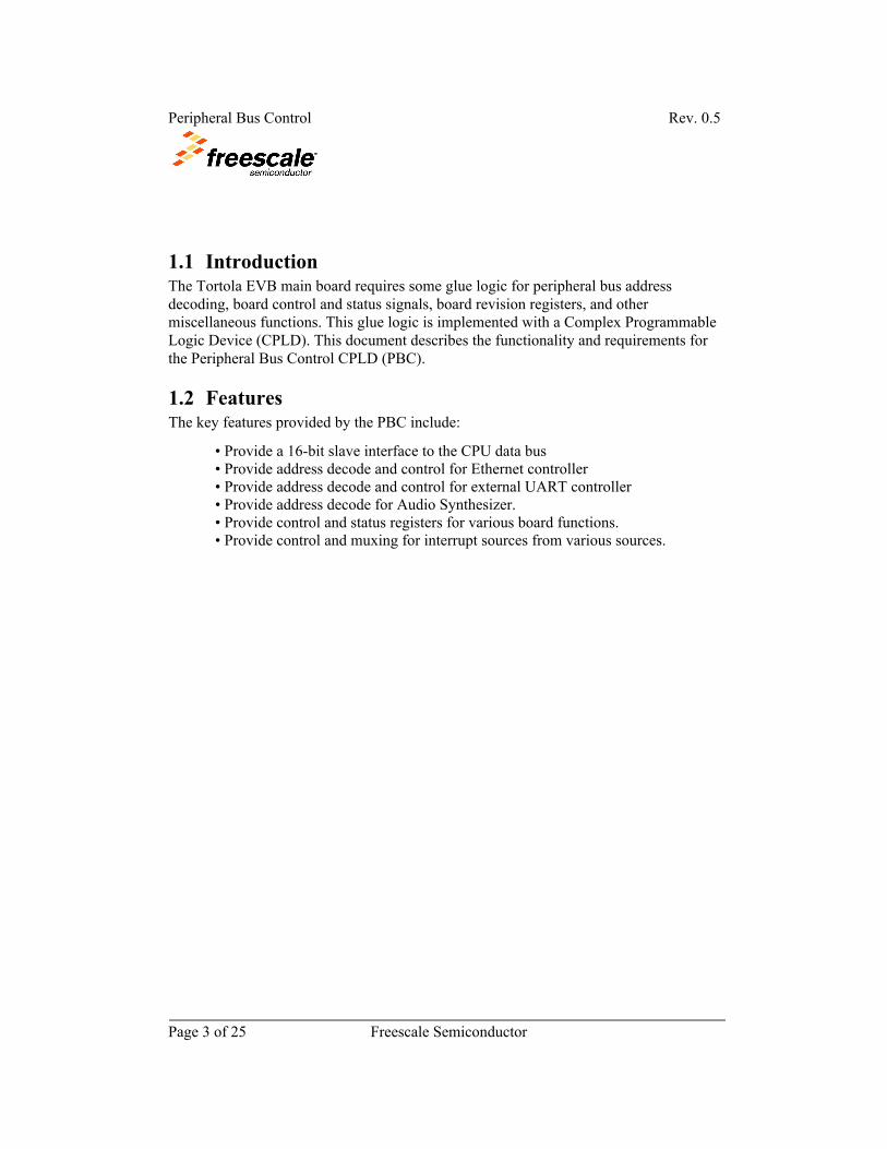
1.10.2 Interrupt Signal Current State Status RegisterThis register represents the current state of each edge triggered interrupt source. This register is a read only register.
Table 20 Interrupt Signal Current State Status Register
NAME Interrupt Current State Status Register
BIT 15 14 13 12 11 10 9 8 7 6 5 4 3 2 1 0
FIELD RES RES RES RES RES RES RES RES RES RES RES RESFSH_OVR
OTG_FS_
OVR
PB_IRQ
LOW_BAT
Table 21 Interrupt Current Status Register Bit Definitions
Settings Description Name
0 - Low Battery indicationLow Battery— Low Battery Indicator signal from Atlas LOW_BAT1- Normal operationBoard. Bit 4
0 – Push button is pressedPush Button IRQ — Push button switch circuit.PB_IRQ1- Push button is not pressedBit 5
0 – Over Current indicationUSB OTG Full Speed Over Current —USB OTG Full OTG_FS_OVR
1- No Over Current indicationSpeed Over Current indication.Bit 6
0 – Over Current indicationUSB Full Speed Host Over Current — The USB Full SpeedFSH_OVR
1- No Over Current indicationHost interface. Over current indication.Bit 7
Peripheral Bus Control Rev. 0.5
Page 22 of 25 Freescale Semiconductor
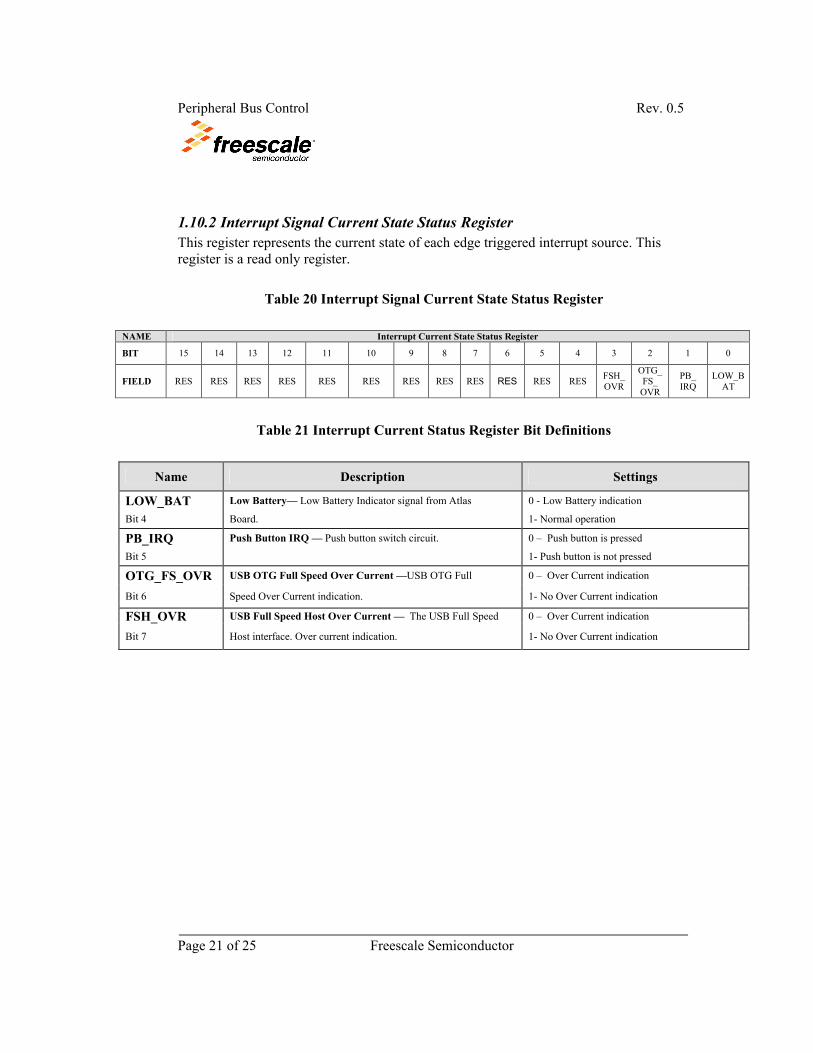
1.10.3 Interrupt Mask Register The Interrupt Mask Register enables/disables the corresponding interrupt source. A high (one) will enable the associated interrupt source. A low (zero) will mask (disable) the associated interrupt source. Even if the interrupt is masked the associated status register bit will still indicate whether or not an interrupt is pending from each source. However a masked interrupt will not cause an interrupt signal to be generated to the GPIO pin it is associated with. Modifying the Mask Register to enable an interrupt that is pending will immediately cause an interrupt to be generated. This register is implemented as a set register and a clear register. To set a bit, the set address is used, writing a 1 to the desired bit. To clear a bit, the clear address is used, writing a 1 to the desired bit.
Table 22 Interrupt Mask Register
NAME Interrupt Mask Register
BIT 15 14 13 12 11 10 9 8 7 6 5 4 3 2 1 0
MASKED INTERRUPT FEILD
RESCE_INT2
CE_INT1
SYNTH_IRQ
XUART_INTB
XUART_INTA
OTG_FS_INT
ENET_INT
RES RES RES RESFSH_OVR
OTG_FS_
OVR
PB_IRQ
LOW_BAT
OPER R/W R/W R/W R/W R/W R/W R/W R/W R/W R/W R/W R/W R/W R/W R/W R/W
RESET 0 0 0 0 0 0 0 0 0 0 0 0 0 0 0 0

Peripheral Bus Control Rev. 0.5
Page 23 of 25 Freescale Semiconductor
1.10.3 GPIO Interrupt Grouping and Non Registered Interrupts Some interrupt signals are not associated with any CPLD register but are instead directly routed (inside the CPLD) to a GPIO pin. The SD and Memory Stick detect functions are logically ORed together since only one or the other should be implemented at any given time. The interrupt are grouped in the following way:
GPIO Interrupt sourcesGPIO1_1 SD1_DET + MS1_DET
GPIO1_2 SD2_DET + MS2_DET
GPIO1_3 PRI_INT (ATLAS)
GPIO1_4 XUART_INTA, XUART_INTB, ENET_INT, LOW_BAT, PB_IRQ, OTG_FS_OVR, OTG_FS_INT, FSH_OVR, SYNTH_IRQ, CE_INT1, CE_INT2
Table 23 GPIO Interrupt Bit Descriptions
Settings Description Name
0 – No Card is insertedSD1 OR MS1 memory card detect statusGPIO1_11- A card has been detected
0 – No Card is insertedSD2 OR MS2 memory card detect statusGPIO1_2
1- A card has been detected
0 – No interrupt pendingAtlas’ Primary Interrupt output status bitGPIO1_31- Interrupt active
0 – No interrupt pendingRegistered Interrupt Status bitGPIO1_41- Interrupt active

Peripheral Bus Control Rev. 0.5
Page 24 of 25 Freescale Semiconductor
1.14 References
[1] ZAS peripheral Bus Control CPLD, November 30, 2004, Version 2.0, Freescale Semiconductor.
[2] CS8900A ISA Ethernet Controller Data Sheet, April 2001, Cirrus Logic.
[3] SC16C652 Dual UART Controller, June 20, 2003, Rev 04, Philips Semiconductors.
[4] ISA System Architecture, October 1993, Mindshare, In