Embed Size (px)
Citation preview

MAHARASHTRA STATE BOARD OF TECHNICAL EDUCATION (Autonomous)
(ISO/IEC - 27001 - 2005 Certified)
WINTER– 14 EXAMINATION
Subject Code: 17541 Model Answer Page No: ____/ N
__________________________________________________________________________________________________
1
Important Instructions to examiners:
1) The answers should be examined by key words and not as word-to-word as given in the
model answer scheme.
2) The model answer and the answer written by candidate may vary but the examiner may try
to assess the understanding level of the candidate.
3) The language errors such as grammatical, spelling errors should not be given more
Importance (Not applicable for subject English and Communication Skills.
4) While assessing figures, examiner may give credit for principal components indicated in the
figure. The figures drawn by candidate and model answer may vary. The examiner may give credit for
any
equivalent figure drawn.
5) Credits may be given step wise for numerical problems. In some cases, the assumed constant
values may vary and there may be some difference in the candidate’s answers and model answer.
6) In case of some questions credit may be given by judgement on part of examiner of relevant answer
based on candidate’s understanding.
7) For programming language papers, credit may be given to any other program based on equivalent
concept.
__________________________________________________________________________________
Q1. A) Attempt any THREE of the following:
(i). Draw symbols of SIT, MCT and FCT. Draw the V-I characteristics of each.
Ans: Symbol- 2 marks each and V-I characteristics: 2 marks each
SIT MCT FCT
MAHARASHTRA STATE BOARD OF TECHNICAL EDUCATION (Autonomous)
(ISO/IEC - 27001 - 2005 Certified)
WINTER– 14 EXAMINATION
Subject Code: 17541 Model Answer Page No: ____/ N
__________________________________________________________________________________________________
2
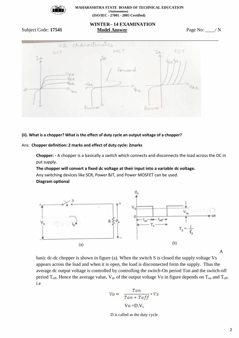
(ii). What is a chopper? What is the effect of duty cycle an output voltage of a chopper?
Ans: Chopper definition: 2 marks and effect of duty cycle: 2marks
Chopper: - A chopper is a basically a switch which connects and disconnects the load across the DC in
put supply.
The chopper will convert a fixed dc voltage at their input into a variable dc voltage.
Any switching devices like SCR, Power BJT, and Power MOSFET can be used.
Diagram optional
A
basic dc-dc chopper is shown in figure (a). When the switch S is closed the supply voltage Vs
appears across the load and when it is open, the load is disconnected form the supply. Thus the
average dc output voltage is controlled by controlling the switch-On period Ton and the switch-off
period Toff. Hence the average value, Vdc of the output voltage Vo in figure depends on Ton and Toff.
i.e
Vo =D.Vs
D is called as the duty cycle
MAHARASHTRA STATE BOARD OF TECHNICAL EDUCATION (Autonomous)
(ISO/IEC - 27001 - 2005 Certified)
WINTER– 14 EXAMINATION
Subject Code: 17541 Model Answer Page No: ____/ N
__________________________________________________________________________________________________
3
As Ton increases , the output voltage Vo increases.
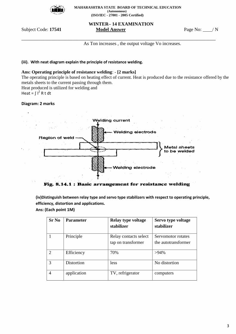
(iii). With neat diagram explain the principle of resistance welding.
Ans: Operating principle of resistance welding: - [2 marks]
The operating principle is based on heating effect of current. Heat is produced due to the resistance offered by the
metals sheets to the current passing through them.
Heat produced is utilized for welding and
Heat = ∫ I2 R t dt
Diagram: 2 marks
(iv)Distinguish between relay type and servo type stabilizers with respect to operating principle,
efficiency, distortion and applications.
Ans: (Each point 1M)
Sr No Parameter Relay type voltage
stabilizer
Servo type voltage
stabilizer
1 Principle Relay contacts select
tap on transformer
Servomotor rotates
the autotransformer
2 Efficiency 70% >94%
3 Distortion less No distortion
4 application TV, refrigerator computers

MAHARASHTRA STATE BOARD OF TECHNICAL EDUCATION (Autonomous)
(ISO/IEC - 27001 - 2005 Certified)
WINTER– 14 EXAMINATION
Subject Code: 17541 Model Answer Page No: ____/ N
__________________________________________________________________________________________________
4
b) Attempt any ONE of the following:
(i) Describe the working of class A chopper using SCR with circuit diagram. Draw the output waveforms.
Ans: Circuit Diagram- 1 mark
Explaination-3 marks
1. Type A chopper operates with periodic opening and closing of S1.
2. S1 and freewheeling diode D1 conduct only in one direction.
3. Assume the load is inductive.
4. When S1 is closed load voltage is positive, load current is also positive and inductor will store energy.
When S1 is commutated, there is a change in current.
5. Inductor opposes this change and reverses it’s polarity.
6. This forward biases the diode D1 and freewheeling action takes place.
Average output voltage and average output current are +ve. Chopper operates in I-quadrant.
Waveforms-2 marks

MAHARASHTRA STATE BOARD OF TECHNICAL EDUCATION (Autonomous)
(ISO/IEC - 27001 - 2005 Certified)
WINTER– 14 EXAMINATION
Subject Code: 17541 Model Answer Page No: ____/ N
__________________________________________________________________________________________________
5
(ii) Draw the circuit diagram and o/p waveforms and explain the working of half –bridge inverter.
Ans: Circuit Diagram- 1 mark,
Explanation-3 marks
Assume the load is resistive.
1. When SCR S1 is turned ON, current flows from the upper source, S1 and the load.
2. When SCR S2 is turned ON, current flows from lower half of the source and S2.
3. The direction of the load current reverses across the load.
4. If the load is inductive, then freewheeling diodes are used.
Waveforms: 2 marks
Q2Attempt any TWO of the following:
a) State the need of series and parallel connections of SCR. Draw neat labeled circuit diagram of three SCRs
connected in series combination. Describe the role of static and dynamic equalizing circuit.
Ans: Need for series and parallel connections of SCR:(any two points-2 marks)
1. The required voltage and current rating are lower than the maximum limits.
2. The designer is forced to use lower rated SCRs for economy and reliability.
3. These lower rated SCRs have to be connected in series and parallel combinations to suit the voltage and
current requirements.
4. Series is used for high voltage low current and parallel is used for low voltage and high current
applications.
MAHARASHTRA STATE BOARD OF TECHNICAL EDUCATION (Autonomous)
(ISO/IEC - 27001 - 2005 Certified)
WINTER– 14 EXAMINATION
Subject Code: 17541 Model Answer Page No: ____/ N
__________________________________________________________________________________________________
6
Diagram-2 marks
STATIC AND DYNAMIC EQUALIZING CIRCUIT
Role of static and dynamic equalizing circuit-4 marks
Consider the case of three SCRs connected in series which have different characteristics.
1. When voltage is applied across such a combination, then the SCR with the highest turn-on time will
share the maximum blocking voltage because the other two SCRs must have already turned on.
2. Similarly when reverse voltage is applied across this string SCR with the least recovery time will go to
the blocking state first and the other two SCRs will still be conducting.
These two conditions are unfavorable. Hence static and dynamic equalizing circuits are used. Static
equalizing circuit consists of a shunt resistor across each SCR. This reduces the effect of unequal blocking
resistances. The dynamic equalizing circuit consists of an R-C snubber circuit and a diode. (It is used to
control the voltage distribution when the SCRs are in the blocking state.) To equalize voltage during
transient state ie during turn on and turn off of SCRs
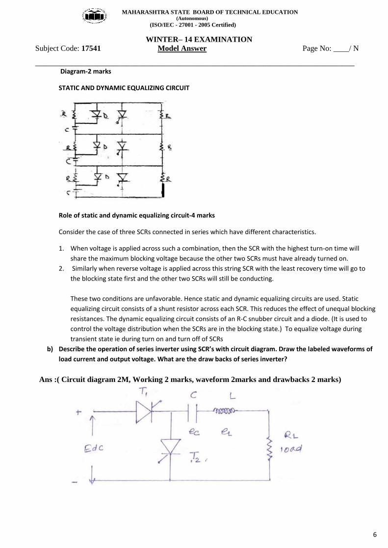
b) Describe the operation of series inverter using SCR’s with circuit diagram. Draw the labeled waveforms of
load current and output voltage. What are the draw backs of series inverter?
Ans :( Circuit diagram 2M, Working 2 marks, waveform 2marks and drawbacks 2 marks)

MAHARASHTRA STATE BOARD OF TECHNICAL EDUCATION (Autonomous)
(ISO/IEC - 27001 - 2005 Certified)
WINTER– 14 EXAMINATION
Subject Code: 17541 Model Answer Page No: ____/ N
__________________________________________________________________________________________________
7
Working:
When S1 (T1) is triggered the capacitor starts charging with left plate positive with respect to right
and when the voltage on capacitor is slightly greater than Edc then T1 turns off; but there is no
discharge path for capacitor hence it holds the charge.
When trigger pulse is applied to T2, then T2 start conducting so current starts flowing in opposite
direction. In this way due to charge and discharge of capacitor and switching of T1 and T2 current
will flow in RC. Hence sinusoidal current starts flowing in the load.
Drawbacks of series inverter
1. The frequency is limited to f= 1/2π√LC
2. SCR 2 should not be turned on when SCR 1 is conducting. This will cause short circuit of the dc
source.
3. Power flow from the source is not continuous.
c) Draw and explain the block diagram of capacitor energy storage welding. State the two advantages and
two disadvantages.
Ans: (Diagram- 2marks, Explanation- 4 marks, Advantages and Disadvantages- 2 marks)
DIAGRAM-
Explanation-
1. It consists of 3 phase rectifier, ignitron contactor, a large value capacitor connected across primary
winding of the welding transformer.
2. The secondary of the welding transformer is connected to 2 electrodes, through which large currents
can pass.
3. 3 phase AC is rectified to DC.
4. A step-up transformer is used to increase the voltage if required.
5. Large value capacitor is charged by the DC which stores the energy.
MAHARASHTRA STATE BOARD OF TECHNICAL EDUCATION (Autonomous)
(ISO/IEC - 27001 - 2005 Certified)
WINTER– 14 EXAMINATION
Subject Code: 17541 Model Answer Page No: ____/ N
__________________________________________________________________________________________________
8
6. The capacitor discharges the stored energy to the electrodes at the time of welding.
7. Discharging takes place through the primary winding of the transformer.
Advantages: 1. Simple circuit
2. Does not cause voltage dip at the time of welding.
Disadvantages-
1. Large value capacitor is required.
2. 3 phase rectifier is used.
Q3 Attempt any Four of the following:
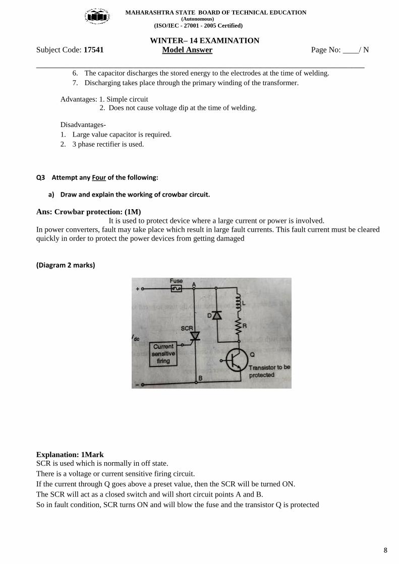
a) Draw and explain the working of crowbar circuit.
Ans: Crowbar protection: (1M)
It is used to protect device where a large current or power is involved.
In power converters, fault may take place which result in large fault currents. This fault current must be cleared
quickly in order to protect the power devices from getting damaged
(Diagram 2 marks)
Explanation: 1Mark SCR is used which is normally in off state.
There is a voltage or current sensitive firing circuit.
If the current through Q goes above a preset value, then the SCR will be turned ON.
The SCR will act as a closed switch and will short circuit points A and B.
So in fault condition, SCR turns ON and will blow the fuse and the transistor Q is protected

MAHARASHTRA STATE BOARD OF TECHNICAL EDUCATION (Autonomous)
(ISO/IEC - 27001 - 2005 Certified)
WINTER– 14 EXAMINATION
Subject Code: 17541 Model Answer Page No: ____/ N
__________________________________________________________________________________________________
9
b) Draw and explain the working of non-isolated SMPS.
Ans: (Diagram- 2 marks, EXPLANATION- 2 marks)
Buck regulator or Boost regulator can be considered as Non-isolated SMPS
BUCK REGULATOR
BUCK REGULATOR-
1. Transistor Q1 connected in series with the load.
2. When it is turned on the DC voltage is connected to the LC filter.
3. The output is constant with the help of capacitor.
4. When Q1 is off inductor’s polarity is reversed, freewheeling diode is forward biased and load current
starts flowing through the circuit.
BOOST REGULATOR-
1. It is also a step-up chopper.
2. When Q1 is ON current through the inductor rises, diode becomes reverse biased, load voltage is zero.
3. When Q1 is OFF inductor reverses its polarity, diode becomes forward biased and voltage is available to
the load which is more than input voltage.
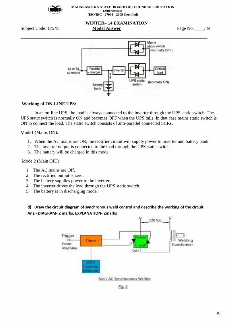
c) Draw the block diagram of ON-LINE UPS and explain the working.
Ans: B.D. of on-line UPS: 02 marks, working: 02 marks
MAHARASHTRA STATE BOARD OF TECHNICAL EDUCATION (Autonomous)
(ISO/IEC - 27001 - 2005 Certified)
WINTER– 14 EXAMINATION
Subject Code: 17541 Model Answer Page No: ____/ N
__________________________________________________________________________________________________
10
Working of ON-LINE UPS:
In an on-line UPS, the load is always connected to the inverter through the UPS static switch. The
UPS static switch is normally ON and becomes OFF when the UPS fails. In that case mains static switch is
ON to connect the load. The static switch consists of anti-parallel connected SCRs.
Mode1 (Mains ON):
1. When the AC mains are ON, the rectifier circuit will supply power to inverter and battery bank.
2. The inverter output is connected to the load through the UPS static switch.
3. The battery will be charged in this mode.
Mode 2 (Main OFF):
1. The AC mains are Off.
2. The rectified output is zero.
3. The battery supplies power to the inverter.
4. The inverter drives the load through the UPS static switch.
5. The battery is in discharging mode.
d) Draw the circuit diagram of synchronous weld control and describe the working of the circuit.
Ans:- DIAGRAM- 2 marks, EXPLANATION- 2marks
MAHARASHTRA STATE BOARD OF TECHNICAL EDUCATION (Autonomous)
(ISO/IEC - 27001 - 2005 Certified)
WINTER– 14 EXAMINATION
Subject Code: 17541 Model Answer Page No: ____/ N
__________________________________________________________________________________________________
11
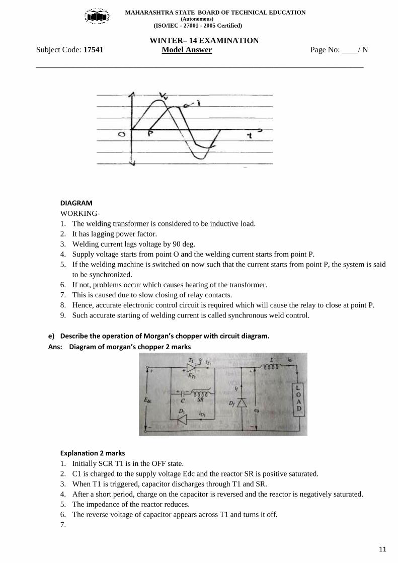
DIAGRAM
WORKING-
1. The welding transformer is considered to be inductive load.
2. It has lagging power factor.
3. Welding current lags voltage by 90 deg.
4. Supply voltage starts from point O and the welding current starts from point P.
5. If the welding machine is switched on now such that the current starts from point P, the system is said
to be synchronized.
6. If not, problems occur which causes heating of the transformer.
7. This is caused due to slow closing of relay contacts.
8. Hence, accurate electronic control circuit is required which will cause the relay to close at point P.
9. Such accurate starting of welding current is called synchronous weld control.
e) Describe the operation of Morgan’s chopper with circuit diagram.
Ans: Diagram of morgan’s chopper 2 marks
Explanation 2 marks
1. Initially SCR T1 is in the OFF state.
2. C1 is charged to the supply voltage Edc and the reactor SR is positive saturated.
3. When T1 is triggered, capacitor discharges through T1 and SR.
4. After a short period, charge on the capacitor is reversed and the reactor is negatively saturated.
5. The impedance of the reactor reduces.
6. The reverse voltage of capacitor appears across T1 and turns it off.
7.

MAHARASHTRA STATE BOARD OF TECHNICAL EDUCATION (Autonomous)
(ISO/IEC - 27001 - 2005 Certified)
WINTER– 14 EXAMINATION
Subject Code: 17541 Model Answer Page No: ____/ N
__________________________________________________________________________________________________
12
Q4. Attempt any THREE of the following:
(i) Describe the operation of single phase cyclo-converter with neat circuit diagram and waveforms.
Ans: Diagram 2 marks (BRIDGE CONFIGURATION)
Figure: Bridge configuration of bridge cyclonator
Waveform:1 mark

MAHARASHTRA STATE BOARD OF TECHNICAL EDUCATION (Autonomous)
(ISO/IEC - 27001 - 2005 Certified)
WINTER– 14 EXAMINATION
Subject Code: 17541 Model Answer Page No: ____/ N
__________________________________________________________________________________________________
13
Explanation: 1 mark
1. CycloConverter reduces the input frequency.
2. Depending upon firing sequence of the SCRs that particular SCR conducts.
3. For example, in the diagram shown, SCRs firing sequence is P1, P2, P1. This forms the single
positive half cycle.
4. For the negative half cycle, firing sequence is NI, N2, N1.
5. The output frequency is reduced to 1/3.
(ii) What is the need for protection circuits for power devices? List different types of protection circuits.
Ans :( Need of protection circuits 2M, types 2M)
Need: To provide protection against over voltage , over current, di/dt, dV/dt, and over temperature.
In the converter circuit voltage transient get generated due to reverse recovery process of the power
devices and switching take place in presence of supply and load inductance. The short circuit fault
condition or the cross conduction taking place in convertor circuit will result in heavy fault current
flowing through the devices. So we require protection circuit.
Diagram of over voltage and over current protection circuits is optional
Different protection circuits: 2 marks
Fuse and circuit breakers are used for over current protection which are power dependent and have
complicated circuit.
Fuse is connected in series and as fault current increases it melts.
Crowbar circuit can also be used for over current protection
di/dt protectionand dv/dt protection provided by snubber circuit
Thyrector selenium diode move MOV can be used for overvoltage protection which are voltage
dependent nonlinear resistors and have simple circuit.
It senses over voltages due to transients or spikes.
Over voltage protection devices are selenium diodes and varistors (Varistors).
Snubber circuits
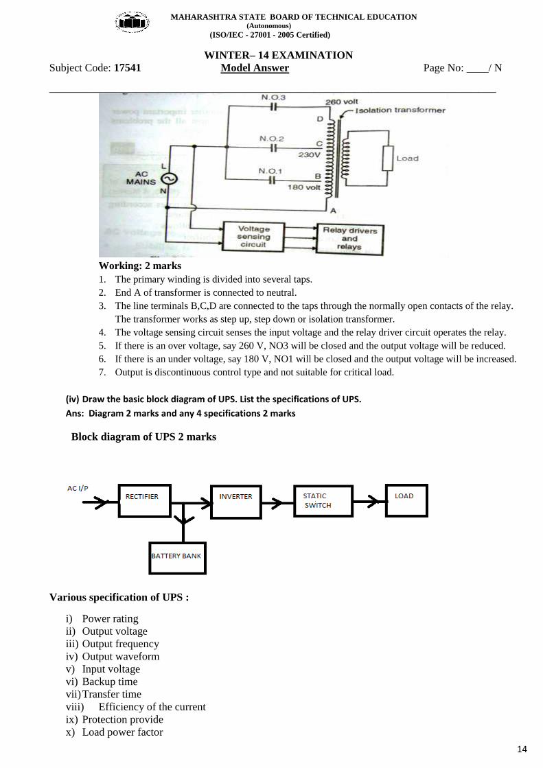
(iii) Draw the circuit of Relay type voltage stabilizer and explain the working.
Ans) Diagram :- (02 marks) Relay type AC voltage stabilizer:-
MAHARASHTRA STATE BOARD OF TECHNICAL EDUCATION (Autonomous)
(ISO/IEC - 27001 - 2005 Certified)
WINTER– 14 EXAMINATION
Subject Code: 17541 Model Answer Page No: ____/ N
__________________________________________________________________________________________________
14
Working: 2 marks
1. The primary winding is divided into several taps.
2. End A of transformer is connected to neutral.
3. The line terminals B,C,D are connected to the taps through the normally open contacts of the relay.
The transformer works as step up, step down or isolation transformer.
4. The voltage sensing circuit senses the input voltage and the relay driver circuit operates the relay.
5. If there is an over voltage, say 260 V, NO3 will be closed and the output voltage will be reduced.
6. If there is an under voltage, say 180 V, NO1 will be closed and the output voltage will be increased.
7. Output is discontinuous control type and not suitable for critical load.
(iv) Draw the basic block diagram of UPS. List the specifications of UPS.
Ans: Diagram 2 marks and any 4 specifications 2 marks
Block diagram of UPS 2 marks
Various specification of UPS :
i) Power rating
ii) Output voltage
iii) Output frequency
iv) Output waveform
v) Input voltage
vi) Backup time
vii) Transfer time
viii) Efficiency of the current
ix) Protection provide
x) Load power factor

MAHARASHTRA STATE BOARD OF TECHNICAL EDUCATION (Autonomous)
(ISO/IEC - 27001 - 2005 Certified)
WINTER– 14 EXAMINATION
Subject Code: 17541 Model Answer Page No: ____/ N
__________________________________________________________________________________________________
15
b) Attempt any ONE of the following:
(i) Draw the circuit diagram of parallel connections of three thyristors and describe with forward
characteristics. Justify symmetrical arrangement of SCR’s.
Ans: (Parallel connection- 1 mark, Forward characteristics- 1 mark, symmetrical arrangement- 1
mark, explanation- 3 marks)
Parallel connection of SCRs-1 mark
FORWARD CHARACTERISTICS-(1 MARK)
SYMMETRICAL ARRANGEMENT- (1 MARK)
EXPLANATION-
1. SCRs are connected in parallel to improve the current rating.
2. Due to unequal dynamic resistance the sharing of current will not be equal which causes
heating of the SCRs and thermal runaway.

MAHARASHTRA STATE BOARD OF TECHNICAL EDUCATION (Autonomous)
(ISO/IEC - 27001 - 2005 Certified)
WINTER– 14 EXAMINATION
Subject Code: 17541 Model Answer Page No: ____/ N
__________________________________________________________________________________________________
16
3. Hence, all the SCRs operated in parallel should be at the same temperature by having a
common heat sink.
4. When operated in parallel there is a problem of unequal flux linkages.
5. SCR which is in the centre will have maximum flux and will share less current. In case of
linear mounting.
6. Hence symmetrical arrangement of SCRs is used which provides equal flux linkage.
(ii). With neat waveforms describe how output voltage and harmonics can be controlled using PWM
control method in inverters.
Ans:-
Note:- Any one method can be considered with diagram 2 marks and explanation 4 marks
The most efficient of controlling the gain and output voltage is to incorporate pulse width modulation
control within the inverter .the commonly used PWM techniques are as follows
1) Single pulse width modulation
2) Sinusoidal pulse width modulation
3) Multiple pulse width modulation
Sinusoidal pulse width modulation : The PWM waveform generated at the output of the controlled circuit
is used to drive transistors or other semiconductor devices connected in the inverter circuit. This type of
modulation is realized by comparing a control signal consisting of rectified sinusoidal wave of variable
magnitude Am and frequency fm= 1/T equal to frequency of inverter & a triangular wave of fixed amplitude
and frequency. The comparator output is high when the magnitude of sine wave is greater than that of
triangular wave. The modulation index of PWM signal is defined as the ratio of: Am/ Ac.The carrier
frequency ratio is defined as the ratio of fc to fm.
This method reduces the harmonics present in the output waveform. A pure quasi square wave is obtained.
For further reduction in harmonics filter can be used.
Types of pulse width modulation:
1) Single Pulse-Width Modulation:- In single -pulse-width modulation control, there is only one
pulse per half-cycle and the width of the pulse is varied to control the inverter output voltage.
MAHARASHTRA STATE BOARD OF TECHNICAL EDUCATION (Autonomous)
(ISO/IEC - 27001 - 2005 Certified)
WINTER– 14 EXAMINATION
Subject Code: 17541 Model Answer Page No: ____/ N
__________________________________________________________________________________________________
17
The gating signals are generated by comparing a rectangular reference signal of amplitude Ar
with a triangular carrier wave of amplitude Ac.
2) Multiple Pulse-Width Modulation:-
In this method of pulse-width modulation, the harmonic content can be reduced using several
pulses in each in each half-cycle of output voltage. By comparing a reference signal with a
triangular carrier wave, the gating signals are generated for turning-on and turning-off of a
thyristor. fc>fm
3) Sinusoidal Pulse-Width Modulation
Instead of maintaining the width of all pulses the same as in the case of multiple-pulse
modulation, the width of each pulse is varied in proportion to the amplitude of a sine wave .The
gating signals are generated by comparing a sinusoidal reference signal with a triangular carrier
wave of frequency fc.
The six-step waveform has a zero-voltage step between the positive and negative sections of
the square wave such that the harmonics that are multiples of three are eliminated . When carrier-
based PWM techniques are applied to six-step waveforms, the basic overall shape, or envelope, of
the waveform is retained so that the 3rd
harmonic and its multiples are cancelled.
Q5) Attempt Any TWO of the following:
a) Draw and explain the working of Jone’s chopper with neat circuit diagram and waveforms.
Ans) (Explanation 02 M, Circuit 03M, Waveforms 03M)
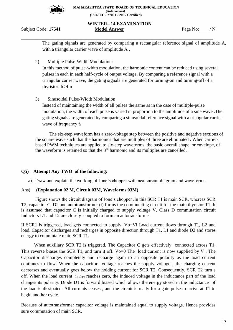
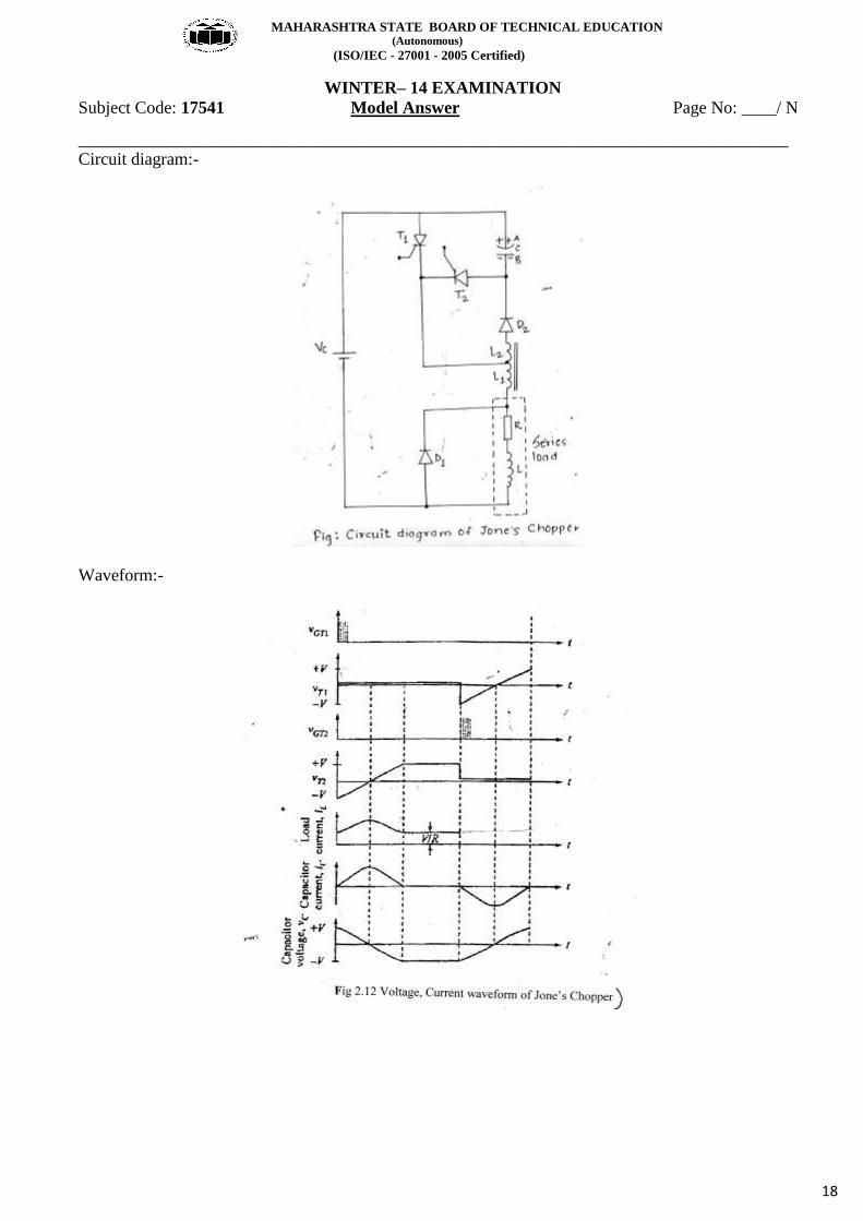
Figure shows the circuit diagram of Jone’s chopper .In this SCR T1 is main SCR, whereas SCR
T2, capacitor C, D2 and autotransformer (t) forms the commutating circuit for the main thyristor T1. It
is assumed that capacitor C is initially charged to supply voltage V. Class D commutation circuit
Inductors L1 and L2 are closely coupled to form an autotransformer
If SCR1 is triggered, load gets connected to supply. Vo=Vi Load current flows through T1, L2 and
load. Capacitor discharges and recharges in opposite direction through T1, L1 and diode D2 and stores
energy to commutate main SCR T1.
When auxiliary SCR T2 is triggered. The Capacitor C gets effectively connected across T1.
This reverse biases the SCR T1, and turn it off. Vo=0 The load current is now supplied by V . The
Capacitor discharges completely and recharge again to an opposite polarity as the load current
continues to flow. When the capacitor voltage reaches the supply voltage , the charging current
decreases and eventually goes below the holding current for SCR T2. Consequently, SCR T2 turn s
off. When the load current iL=iT2 reaches zero, the induced voltage in the inductance part of the load
changes its polarity. Diode D1 is forward biased which allows the energy stored in the inductance of
the load is dissipated. All currents ceases , and the circuit is ready for a gate pulse to arrive at T1 to
begin another cycle.
Because of autotransformer capacitor voltage is maintained equal to supply voltage. Hence provides
sure commutation of main SCR.
MAHARASHTRA STATE BOARD OF TECHNICAL EDUCATION (Autonomous)
(ISO/IEC - 27001 - 2005 Certified)
WINTER– 14 EXAMINATION
Subject Code: 17541 Model Answer Page No: ____/ N
__________________________________________________________________________________________________
18
Circuit diagram:-
Waveform:-

MAHARASHTRA STATE BOARD OF TECHNICAL EDUCATION (Autonomous)
(ISO/IEC - 27001 - 2005 Certified)
WINTER– 14 EXAMINATION
Subject Code: 17541 Model Answer Page No: ____/ N
__________________________________________________________________________________________________
19
b) Explain the principle and operation of isolated SMPS. State two advantages and disadvantages.
Ans) (Principle & Operation 04M, Advantage 02M, Disadvantage 02M)
(Note:- Marks should be credited for answer of any type of isolated SMPS)
Circuit Diagram:-
Waveform:-

MAHARASHTRA STATE BOARD OF TECHNICAL EDUCATION (Autonomous)
(ISO/IEC - 27001 - 2005 Certified)
WINTER– 14 EXAMINATION
Subject Code: 17541 Model Answer Page No: ____/ N
__________________________________________________________________________________________________
20
Mode I(t0-t1) :
When transistor Q1 is ON at t=0, primary current starts to build up in the primary winding, storing
energy. Due to the opposite primary arrangement between the input & output windings of the
transformer choke, there is no energy transferred to the load since diode D is reversed biased.
Transistor Q1 is turned off abruptly at instant t=t1. The equivalent circuit for this mode is shown in
figure
Mode II(t1-t2):
When the transistor is turned off at t=t1, the polarity of the windings reverses due to the collapsing
magnetic field. Now , diode D is conducting , charging the output capacitor C and delivering current IL
to load .The voltage across Q1 is the sum of input supply voltage (Edc) and the self induced voltage
across the primary winding (Ldi/dt) , therfore it is higher than the supply voltage (Edc). The equivalent
circuit for this mode is shown in figure . The secondary current goes to zero at t=t2 . Thus the stored
energy in the transformer core is deliverd to load during this mode of operation.
Mode III(t2-t3):
In this mode transistor and diode both are in the off state.Therefore, primary and secondary currents
are zero. As there is no voltage drop across primary winding of the transformer, the voltage across the
transistor Q1 is equal to the dc supply voltage(Edc). The secondary voltage is zero. The one cycle
operation completes in this mode and repeats it self.
Advantages : (any 2)
1. Slower diodes can be used on the secondary side for rectification
2. Size of transformer is smaller than that in the continuous mode
3. Fast Transient response
4. An additional filter inductance is not required on the secondary side
Disadvantage: (any 2)
1. Peak current rating of both devices is high
2. Large size filter capacitor is required
3. The maximum value of duty cycle is limited to 50% to avoid core saturation

MAHARASHTRA STATE BOARD OF TECHNICAL EDUCATION (Autonomous)
(ISO/IEC - 27001 - 2005 Certified)
WINTER– 14 EXAMINATION
Subject Code: 17541 Model Answer Page No: ____/ N
__________________________________________________________________________________________________
21
c) Draw and explain the working of parallel inverter using SCRs with circuit diagram and O/p voltage
and load circuit waveforms.
Ans) (explanation 02M,Circuit 03 M, Waveform 03M)
Parallel Inverter using SCR:-
In the parallel inverter the commutating component are connected in parallel
with the load, where a capacitor connected in parallel with the load is used to commutate a conducting
thyristor by applying reverse voltage across the thyristor. An inductor L is required in series with the
dc source to prevent the instant discharging of capacitor C via the source when the thyristor switching
occurs.
Figure show the basic parallel inverter circuit. This circuit can produce ac square wave output from
dc source.
Circuit Diagram:-
Waveform:-

MAHARASHTRA STATE BOARD OF TECHNICAL EDUCATION (Autonomous)
(ISO/IEC - 27001 - 2005 Certified)
WINTER– 14 EXAMINATION
Subject Code: 17541 Model Answer Page No: ____/ N
__________________________________________________________________________________________________
22
Explaination:-
When T1 is fired and current flows through the inductance L and thyristor T1, the
d.c source voltage Edc appears across half the transformer primary which means the total primary
voltage is 2Edc hence the capacitor is charged to 2Edc with the polarity shown in figure.
When T2 is turn on the commutating capacitor applies a voltage -2Edc to appear
across T1. When this reverse voltage is applied for sufficient time across T1, it will be turn off. SCR
T2 will now be conducting and a voltage of 2Edc will appear across the transformer primary and the
commutating capacitor , but with a reverse polarity.
When T1 is turned on the commutating capacitor applies a voltage -2Edc to appear
across T2, hence it will turn off. Thus, if trigger pulses are periodically applied to the alternate
thyristors, an approximately rectangular voltage waveform will be obtained at the transformer output
terminals
Q6.) Attempt any Four of the following:
a) Draw the equivalent circuit of MCT and explain the working.
Ans) (Circuit diagram 02 M, Explanation 02M)
Circuit Diagram:- MCT could be NMCT or PMCT
Fig: circuit diagram of MCT
MAHARASHTRA STATE BOARD OF TECHNICAL EDUCATION (Autonomous)
(ISO/IEC - 27001 - 2005 Certified)
WINTER– 14 EXAMINATION
Subject Code: 17541 Model Answer Page No: ____/ N
__________________________________________________________________________________________________
23
MCT turn ON:
If the gate of the MCT is negative with respect to anode a p-channel is created in p-
FET and p-channel ON FET causes the forward biasing of n-p-n transistor.(base drive to n-p-n
transistor), the n-p-n transistor applies base drive to p-n-p transistor and regenerative action starts and
the device is latched(turns ON).
MCT turn OFF :
If the gate of MCT is positive with respect to anode, turn off the ON FET and n-
channel is created in n-FET and n-channel FET turns ON which short circuit the base emitter junction
of p-n-p transistor, this diverts the base drive of the transistor through OFF FET and breaks the
regenerative process and the device will turn off.
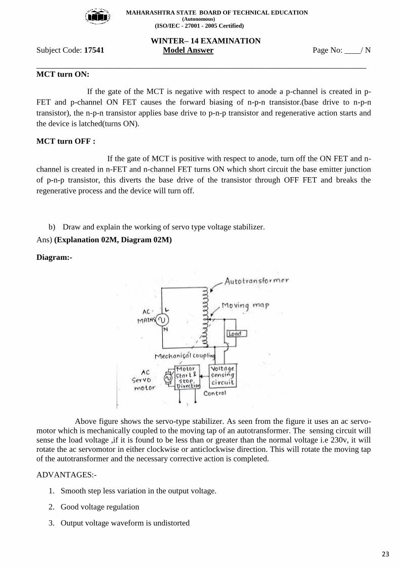
b) Draw and explain the working of servo type voltage stabilizer.
Ans) (Explanation 02M, Diagram 02M)
Diagram:-
Above figure shows the servo-type stabilizer. As seen from the figure it uses an ac servo-
motor which is mechanically coupled to the moving tap of an autotransformer. The sensing circuit will
sense the load voltage ,if it is found to be less than or greater than the normal voltage i.e 230v, it will
rotate the ac servomotor in either clockwise or anticlockwise direction. This will rotate the moving tap
of the autotransformer and the necessary corrective action is completed.
ADVANTAGES:-
1. Smooth step less variation in the output voltage.
2. Good voltage regulation
3. Output voltage waveform is undistorted
MAHARASHTRA STATE BOARD OF TECHNICAL EDUCATION (Autonomous)
(ISO/IEC - 27001 - 2005 Certified)
WINTER– 14 EXAMINATION
Subject Code: 17541 Model Answer Page No: ____/ N
__________________________________________________________________________________________________
24
Disadvantages:-
1. Due to the use of autotransformer and ac servomotor circuit is costly
2. It is not very fast in action
Application:-
1. Mostly for computers
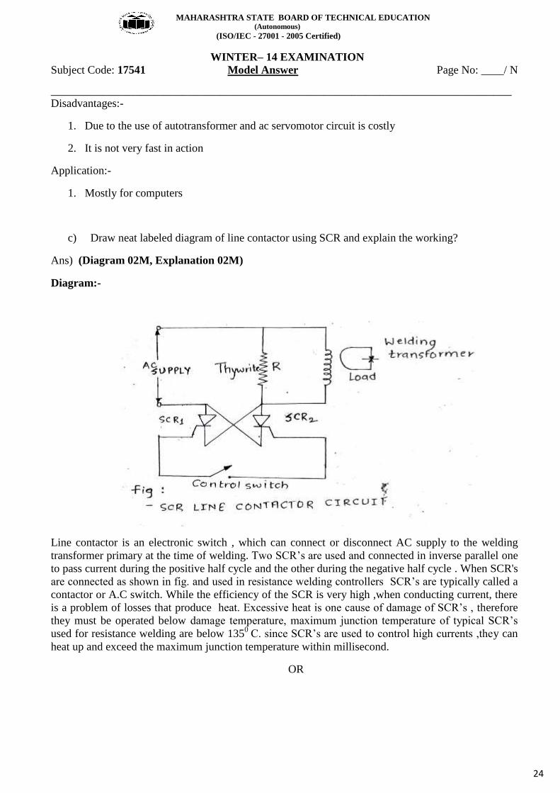
c) Draw neat labeled diagram of line contactor using SCR and explain the working?
Ans) (Diagram 02M, Explanation 02M)
Diagram:-
Line contactor is an electronic switch , which can connect or disconnect AC supply to the welding
transformer primary at the time of welding. Two SCR’s are used and connected in inverse parallel one
to pass current during the positive half cycle and the other during the negative half cycle . When SCR's
are connected as shown in fig. and used in resistance welding controllers SCR’s are typically called a
contactor or A.C switch. While the efficiency of the SCR is very high ,when conducting current, there
is a problem of losses that produce heat. Excessive heat is one cause of damage of SCR’s , therefore
they must be operated below damage temperature, maximum junction temperature of typical SCR’s
used for resistance welding are below 1350
C. since SCR’s are used to control high currents ,they can
heat up and exceed the maximum junction temperature within millisecond.
OR

MAHARASHTRA STATE BOARD OF TECHNICAL EDUCATION (Autonomous)
(ISO/IEC - 27001 - 2005 Certified)
WINTER– 14 EXAMINATION
Subject Code: 17541 Model Answer Page No: ____/ N
__________________________________________________________________________________________________
25
The two SCR’s T1 & T2 are line contactors. During negative half cycle the SCR circuit
carries current via negative supply N-A1-K2-S1-Fuse-D1-K1-A2-transformer-M, when the circuit is
complete , gate current fires SCR T1 & it becomes ‘on’ .the main current now flows through SCR T1
and then through the welding transformer. Similarly during positive half cycle, SCR current flows M-
transformer-A2 -K1-D2-Fuse-S1-D3-K2-A1-N.This makes SCR T2 to ’ON’ & current flows through
Anode to Cathode. Whenever the SCR fires , welding current flows in secondary circuit ,but here the
control is done manually. In circuits requiring heat control ,the firing of SCR is done by phase-shift
bridge network.
d) Define the battery parameters : Back up time & Transfer time.
Ans)
Back up time : ( 2marks)
It is the time period for which the UPS system can supply power to the load , after mains failure
has taken place.
Transfer time : (2marks)
It is the time taken by the UPS system to Switch from mains to battery is known as the transfer
time.
e) What is snubber circuit ? List the types of snubber circuits and draw the circuit diagram of any
one type.
Ans: (definition 01M, List the Types 01M, Diagram 02M)
Snubber Circuit:-
A snubber is a devise used to suppress such as, voltage transients in electrical systems.
Snubber circuit is required in order to suppress the rate of rise of forward voltage i.e. dv/dt across
thyristor , limit di/dt and over voltage during turn on and off.

MAHARASHTRA STATE BOARD OF TECHNICAL EDUCATION (Autonomous)
(ISO/IEC - 27001 - 2005 Certified)
WINTER– 14 EXAMINATION
Subject Code: 17541 Model Answer Page No: ____/ N
__________________________________________________________________________________________________
26
Types of snubber circuit :
1) RC snubber
i) Polarized
ii) Unpolarized.
2) Polarized snubber
i) Forward polarized
ii) Reverse polarized
Diagram:- (Any one)
Figure: Reverse Polarized snubber circuit
OR
Figure: D type snubber circuit

MAHARASHTRA STATE BOARD OF TECHNICAL EDUCATION (Autonomous)
(ISO/IEC - 27001 - 2005 Certified)
WINTER– 14 EXAMINATION
Subject Code: 17541 Model Answer Page No: ____/ N
__________________________________________________________________________________________________
27
OR
.
Figure: Polarized snubber circuit
OR
Figure: Unpolarized Snubber Circuit