Embed Size (px)
Citation preview

第 1 頁,共 23 頁
Winstar Display Co., LTD
華凌光電股份有限公司華凌光電股份有限公司華凌光電股份有限公司華凌光電股份有限公司
住址住址住址住址: 407台中市中清路台中市中清路台中市中清路台中市中清路 163號號號號 No.163 Chung Ching RD., Taichune, Taiwan, R.O.C
WEB: http://www.winstar.com.tw E-mail: [email protected] Tel:886-4-24262208 Fax:886-4-24262207
SPECIFICATION
CUSTOMER :
MODULE NO.: WF320240C-TXI#
APPROVED BY:
( FOR CUSTOMER USE ONLY )
PCB VERSION: DATA:
SALES BY APPROVED BY CHECKED BY PREPARED BY
ISSUED DATE:
第 2 頁,共 23 頁
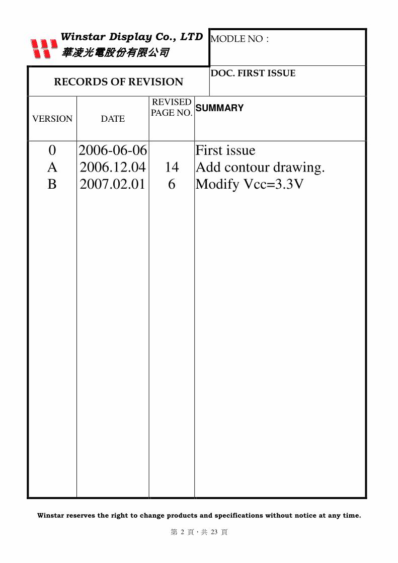
Winstar Display Co., LTD
華凌光電股份有限公司華凌光電股份有限公司華凌光電股份有限公司華凌光電股份有限公司
MODLE NO:
RECORDS OF REVISION DOC. FIRST ISSUE
VERSION DATE
REVISED PAGE NO. SUMMARY
0 A B
2006-06-06 2006.12.04 2007.02.01
14 6
First issue Add contour drawing. Modify Vcc=3.3V
Winstar reserves the right to change products and specifications without notice at any time.

第 3 頁,共 23 頁
ContentsContentsContentsContents
1. Module Classification Information
2. Block Diagram
3. Electrical Characteristics
4. Absolute Maximum Ratings
5. Interface Pin Function
6. Timing Characteristics
7. Optical Characteristics
8. Contour Drawing
9. Inspection specification
10. software (Register Initiate code)
第 4 頁,共 23 頁
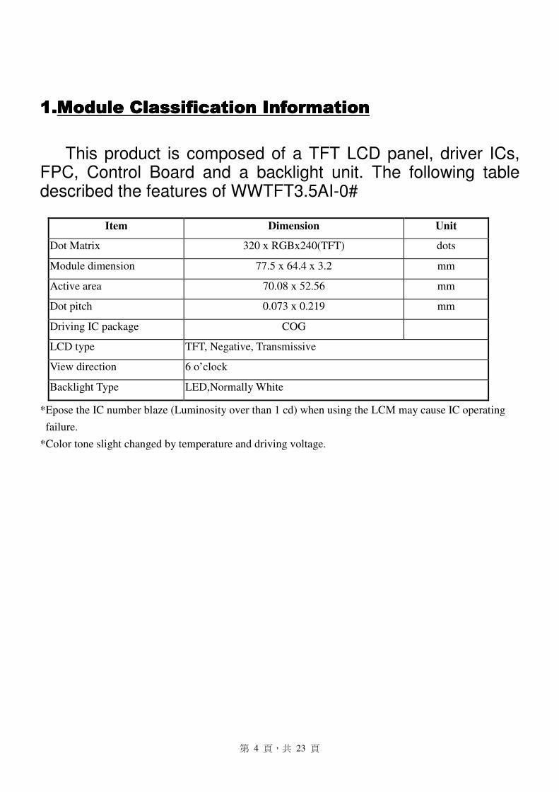
1111....ModModModModule Classification Informationule Classification Informationule Classification Informationule Classification Information
This product is composed of a TFT LCD panel, driver ICs, FPC, Control Board and a backlight unit. The following table described the features of WWTFT3.5AI-0#
Item Dimension Unit
Dot Matrix 320 x RGBx240(TFT) dots
Module dimension 77.5 x 64.4 x 3.2 mm
Active area 70.08 x 52.56 mm
Dot pitch 0.073 x 0.219 mm
Driving IC package COG
LCD type TFT, Negative, Transmissive
View direction 6 o’clock
Backlight Type LED,Normally White
*Epose the IC number blaze (Luminosity over than 1 cd) when using the LCM may cause IC operating
failure.
*Color tone slight changed by temperature and driving voltage.

第 5 頁,共 23 頁
2222....Block DiagramBlock DiagramBlock DiagramBlock Diagram
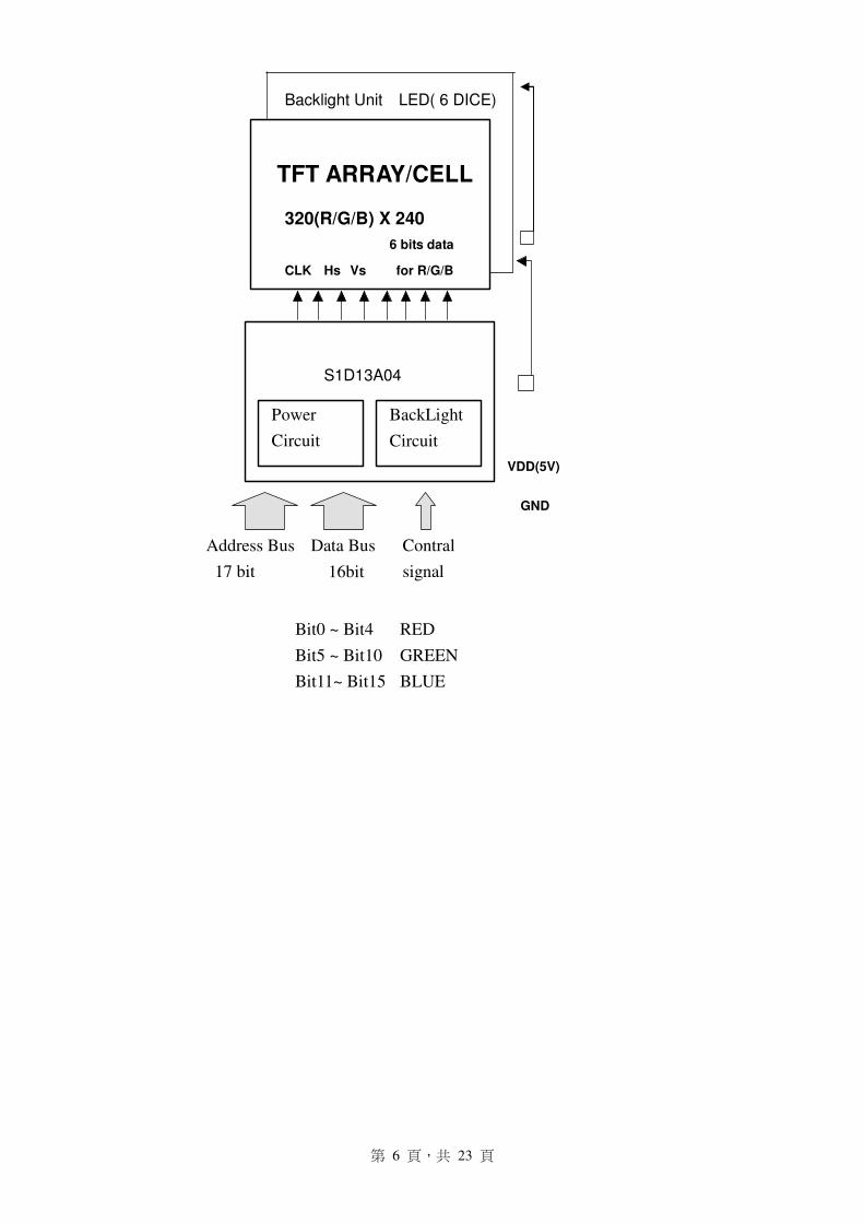
第 6 頁,共 23 頁
TFT ARRAY/CELL
6 bits data
for R/G/B Hs Vs
VDD(5V)
Backlight Unit LED( 6 DICE)
320(R/G/B) X 240
GND
S1D13A04
Contral
signal
CLK
Data Bus
16bit
Power
Circuit
BackLight
Circuit
Address Bus
17 bit
Bit0 ~ Bit4 RED
Bit5 ~ Bit10 GREEN
Bit11~ Bit15 BLUE
第 7 頁,共 23 頁
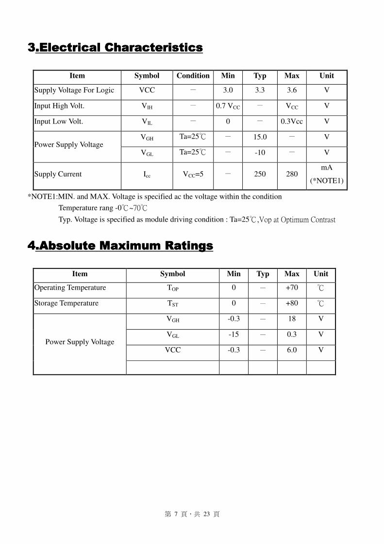
3333.Electrical Characteristics.Electrical Characteristics.Electrical Characteristics.Electrical Characteristics
Item Symbol Condition Min Typ Max Unit
Supply Voltage For Logic VCC - 3.0 3.3 3.6 V
Input High Volt. VIH - 0.7 VCC - VCC V
Input Low Volt. VIL - 0 - 0.3Vcc V
VGH Ta=25℃ - 15.0 - V Power Supply Voltage
VGL Ta=25℃ - -10 - V
Supply Current Icc VCC=5 - 250 280 mA
(*NOTE1)
*NOTE1:MIN. and MAX. Voltage is specified ac the voltage within the condition
Temperature rang -0℃~70℃
Typ. Voltage is specified as module driving condition : Ta=25℃,Vop at Optimum Contrast
4444.Absolute Maximum Ratings.Absolute Maximum Ratings.Absolute Maximum Ratings.Absolute Maximum Ratings
Item Symbol Min Typ Max Unit
Operating Temperature TOP 0 - +70 ℃
Storage Temperature TST 0 - +80 ℃
VGH -0.3 - 18 V
VGL -15 - 0.3 V
VCC -0.3 - 6.0 V Power Supply Voltage

第 8 頁,共 23 頁
5555.Interface Pin Function.Interface Pin Function.Interface Pin Function.Interface Pin Function
5-1 Pins Connection To Control Board
P/N Symbol Function P/N Symbol Function
1 Vcc Power Supply : +5V 26 GND Ground for logic circuit
2 BL_C Backlight control signal 27 NC No Connection
3 DB0 28 GND Ground for logic circuit
4 DB1 29 AD0 System address bus bits
5 DB2 30 GND Ground for logic circuit
6 DB3 31 AD1 System address bus bits
7 DB4 32 GND Ground for logic circuit
8 DB5 33 AD2 System address bus bits
9 DB6 34 GND Ground for logic circuit
10 DB7 35 AD3 System address bus bits
11 DB8 36 GND Ground for logic circuit
12 DB9 37 AD4
13 DB10 38 AD5
14 DB11 39 AD6
15 DB12 40 AD7
16 DB13 41 AD8
17 DB14 42 AD9
18 DB15
Input data from the system data
bus.
43 AD10
19 CS Chip select input. 44 AD11
20 MR See Note(1) 45 AD12
21 RD this pin inputs the read command 46 AD13
22 WR write enable signal 47 AD14
23 BHE This pin inputs the byte enable
signal for the high data byte
48 AD15
24 REST Active low input to set all internal
registers to the default state
49 AD16
25 WAIT This pin outputs the wait signal 50 AD17
System address bus bits
Note(1): This input pin is used to select between the display buffer and register address spaces of the S1D13A04. M/R# is set high to access the display buffer and low to access the registers.

第 9 頁,共 23 頁
6666....Timing CharacteristicsTiming CharacteristicsTiming CharacteristicsTiming Characteristics
6666----1.1.1.1.Interface TimingInterface TimingInterface TimingInterface Timing

第 10 頁,共 23 頁
6666----2.2.2.2. Interface Truth Table for Little EndianInterface Truth Table for Little EndianInterface Truth Table for Little EndianInterface Truth Table for Little Endian

第 11 頁,共 23 頁
7777.Optical Characteristics.Optical Characteristics.Optical Characteristics.Optical Characteristics

第 12 頁,共 23 頁
7.1 Definition of optical characteristics

第 13 頁,共 23 頁

第 1
4 頁,共
23 頁
8.Contour Drawing
WF320240C
39.56
4-O3.5 PTH
9.62
6.22
8.1
66.4
4¡Ó0.
5
54
55.6
(VA
)
52.5
6(A
A)
3.75
7.19
10.2
11.71
93.5¡Ó0.5
86
79.12
73.1(VA)
70.08(AA) 7.96
LCM DRAWING
Nina 06/01/06'
WINSTAR DISPLAY CO.華凌光電股份有限公司華凌光電股份有限公司華凌光電股份有限公司華凌光電股份有限公司
1/1
mm1/1
0
37
3938
GND26
32
3635
3334
29
3130
2827
AD1GNDAD0
40
CLKGND
GNDAD2GNDAD3GNDAD4AD5AD6AD7MR
RDWRBHE
CS
WAITREST
DB13DB14DB15
DB12DB11DB10DB9DB8DB7DB6DB5DB4
DB0GND
15
21
2524
2223
18
2019
17
16
DB1DB2DB3
23
56
4
98
1011
7
1 5V
1314
12
4142
4445
43
4847
4950
46
AD10AD9AD8
AD16AD17
AD11
AD15AD14AD13AD12

第 1
5 頁,共
23 頁
24.35
9.2
20.2
5
65.55
4-O2.5PTH4-O5.0PAD
65(P
CB
)
78.2(PCB)
2.5
2.5
60
73.2
1
50
1 60
0
1/1mm
1/1
華凌光電股份有限公司華凌光電股份有限公司華凌光電股份有限公司華凌光電股份有限公司WINSTAR DISPLAY CO.
Nina 06/01/06'
LCM DRAWING
WF320240C

第 16 頁,共 23 頁
9. Inspection specification
NO Item Criterion AQL
01 Electrical Testing
1.1 Missing vertical, horizontal segment, segment contrast defect. 1.2 Missing character , dot or icon. 1.3 Display malfunction. 1.4 No function or no display. 1.5 Current consumption exceeds product specifications. 1.6 LCD viewing angle defect. 1.7 Mixed product types. 1.8 Contrast defect.
0.65
02 Black or white spots on LCD (display only)
2.1 White and black spots on display ≦0.25mm, no more than
three white or black spots present. 2.2 Densely spaced: No more than two spots or lines within 3mm
2.5
3.1 Round type : As following drawing Φ=( x + y ) / 2
SIZE Acceptable Q TY
Φ≦0.10 Accept no dense
0.10<Φ≦0.20 2
0.20<Φ≦0.25 1
0.25<Φ 0
2.5
03
LCD black spots, white
spots, contamination (non-display)
3.2 Line type : (As following drawing)
Length Width Acceptable Q TY --- W≦0.02 Accept no dense
L≦3.0 0.02<W≦0.03 L≦2.5 0.03<W≦0.05
2
--- 0.05<W As round type
2.5
04 Polarizer bubbles
If bubbles are visible, judge using black spot specifications, not easy to find, must check in specify direction.
Size Φ Acceptable Q TY
Φ≦0.20 Accept no dense
0.20<Φ≦0.50 3
0.50<Φ≦1.00 2
1.00<Φ 0 Total Q TY 3
2.5
第 17 頁,共 23 頁
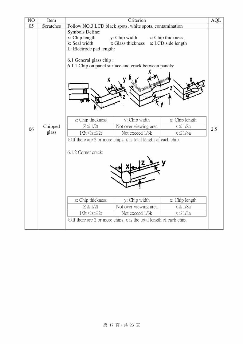
NO Item Criterion AQL 05 Scratches Follow NO.3 LCD black spots, white spots, contamination
06 Chipped
glass
Symbols Define: x: Chip length y: Chip width z: Chip thickness k: Seal width t: Glass thickness a: LCD side length L: Electrode pad length: 6.1 General glass chip : 6.1.1 Chip on panel surface and crack between panels:
z: Chip thickness y: Chip width x: Chip length
Z≦1/2t Not over viewing area x≦1/8a
1/2t<z≦2t Not exceed 1/3k x≦1/8a
☉If there are 2 or more chips, x is total length of each chip.
6.1.2 Corner crack:
z: Chip thickness y: Chip width x: Chip length
Z≦1/2t Not over viewing area x≦1/8a
1/2t<z≦2t Not exceed 1/3k x≦1/8a
☉If there are 2 or more chips, x is the total length of each chip.
2.5
第 18 頁,共 23 頁
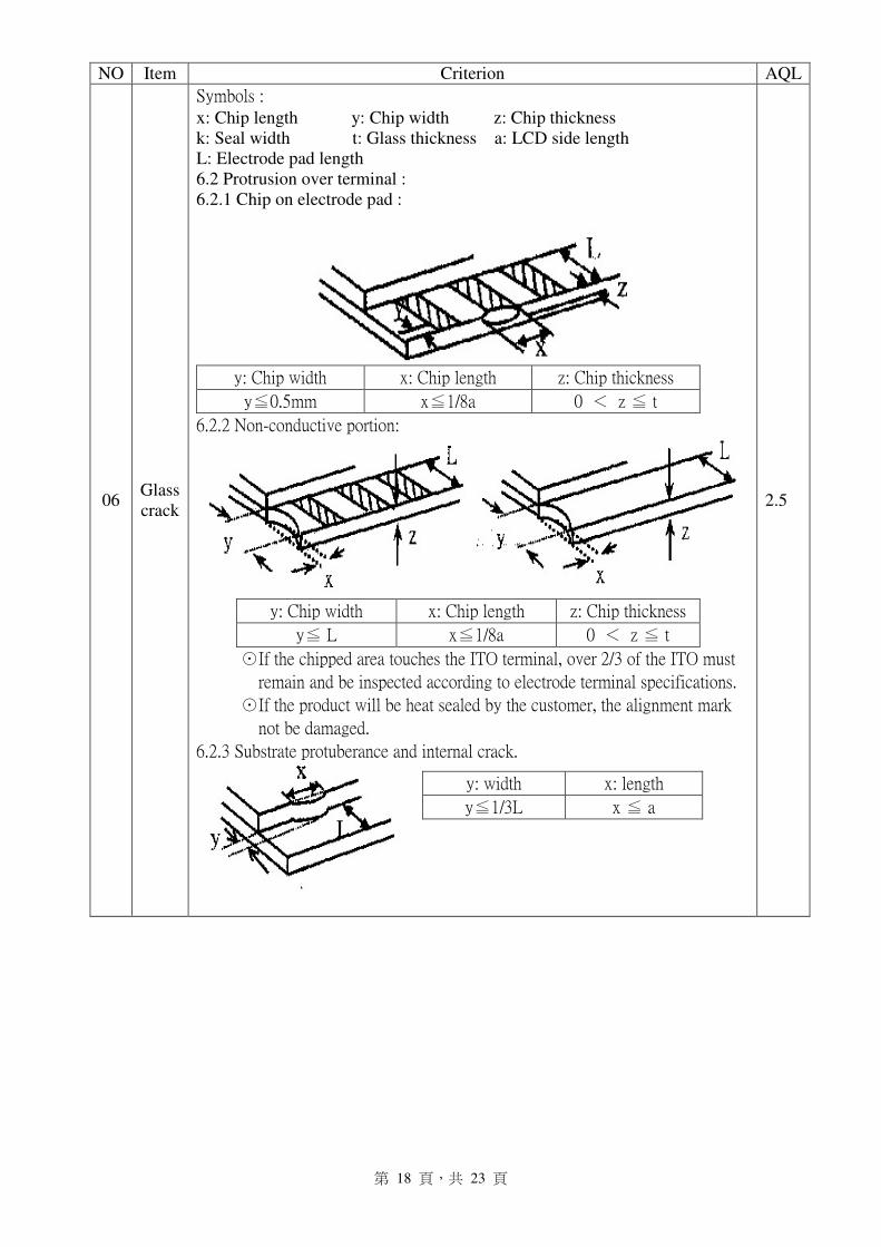
NO Item Criterion AQL
06 Glass crack
Symbols :
x: Chip length y: Chip width z: Chip thickness k: Seal width t: Glass thickness a: LCD side length L: Electrode pad length 6.2 Protrusion over terminal : 6.2.1 Chip on electrode pad :
y: Chip width x: Chip length z: Chip thickness
y≦0.5mm x≦1/8a 0 < z ≦ t
6.2.2 Non-conductive portion:
y: Chip width x: Chip length z: Chip thickness
y≦ L x≦1/8a 0 < z ≦ t
☉If the chipped area touches the ITO terminal, over 2/3 of the ITO must
remain and be inspected according to electrode terminal specifications.
☉If the product will be heat sealed by the customer, the alignment mark
not be damaged.
6.2.3 Substrate protuberance and internal crack.
y: width x: length
y≦1/3L x ≦ a
2.5

第 19 頁,共 23 頁
NO Item Criterion AQL
07 Cracked glass The LCD with extensive crack is not acceptable. 2.5
08 Backlight elements
8.1 Illumination source flickers when lit.
8.2 Spots or scratched that appear when lit must be judged. Using
LCD spot, lines and contamination standards.
8.3 Backlight doesn’t light or color wrong.
0.65 2.5 0.65
09 Bezel
9.1 Bezel may not have rust, be deformed or have fingerprints, stains
or other contamination.
9.2 Bezel must comply with job specifications.
2.5 0.65
10 PCB、COB
10.1 COB seal may not have pinholes larger than 0.2mm or
contamination.
10.2 COB seal surface may not have pinholes through to the IC.
10.3 The height of the COB should not exceed the height indicated in the assembly diagram.
10.4 There may not be more than 2mm of sealant outside the seal area on the PCB. And there should be no more than three places.
10.5 No oxidation or contamination PCB terminals. 10.6 Parts on PCB must be the same as on the production
characteristic chart. There should be no wrong parts, missing parts or excess parts.
10.7 The jumper on the PCB should conform to the product characteristic chart.
10.8 If solder gets on bezel tab pads, LED pad, zebra pad or screw hold pad, make sure it is smoothed down.
2.5 2.5 0.65 2.5 2.5 0.65 0.65 2.5
11 Soldering
11.1 No un-melted solder paste may be present on the PCB.
11.2 No cold solder joints, missing solder connections, oxidation or
icicle.
11.3 No residue or solder balls on PCB.
11.4 No short circuits in components on PCB.
2.5 2.5 2.5 0.65

第 20 頁,共 23 頁
NO Item Criterion AQL
12 General
appearance
12.1 No oxidation, contamination, curves or, bends on interface Pin
(OLB) of TCP.
12.2 No cracks on interface pin (OLB) of TCP.
12.3 No contamination, solder residue or solder balls on product.
12.4 The IC on the TCP may not be damaged, circuits.
12.5 The uppermost edge of the protective strip on the interface pin
must be present or look as if it cause the interface pin to sever.
12.6 The residual rosin or tin oil of soldering (component or chip
component) is not burned into brown or black color.
12.7 Sealant on top of the ITO circuit has not hardened.
12.8 Pin type must match type in specification sheet.
12.9 LCD pin loose or missing pins.
12.10 Product packaging must the same as specified on packaging
specification sheet.
12.11 Product dimension and structure must conform to product
specification sheet.
2.5 0.65 2.5 2.5 2.5 2.5 2.5 0.65 0.65 0.65 0.65

第 21 頁,共 23 頁
10. software (Register Initiate code)
struct easy code S1D_REGS[]= { { 0x14, 0x00000000 }, /* Power Save Configuration Register */ \ { 0x64, 0x28D70000 }, /* GPIO Status and Control Register */ \ { 0x04, 0x00000000 }, /* Memory Clock Configuration Register */ \ { 0x08, 0x00000032 }, /* Pixel Clock Configuration Register */ \ { 0x0C, 0x00000061 }, /* Panel Type and MOD Rate Register */ \ { 0x10, 0x00000010 }, /* Display Settings Register */ \ { 0x20, 0x00000037 }, /* Horizontal Total Register */ \ { 0x24, 0x00000027 }, /* Horizontal Display Period Register */ \ { 0x28, 0x0000000F }, /* Horizontal Display Period Start Position Register */ \ { 0x2C, 0x00870156 }, /* FPLINE Register */ \ { 0x30, 0x00000105 }, /* Vertical Total Register */ \ { 0x34, 0x000000EF }, /* Vertical Display Period Register */ \ { 0x38, 0x0000000D }, /* Vertical Display Period Start Position Register */ \ { 0x3C, 0x00800000 }, /* FPFRAME Register */ \ { 0x40, 0x00000000 }, /* Main Window Display Start Address Register */ \ { 0x44, 0x000000A0 }, /* Main Window Line Address Offset Register */ \ { 0x50, 0x00000000 }, /* PIP+ Window Display Start Address Register */ \ { 0x54, 0x000000A0 }, /* PIP+ Window Line Address Offset Register */ \ { 0x58, 0x00000000 }, /* PIP+ Window X Positions Register */ \ { 0x5C, 0x00000000 }, /* PIP+ Window Y Positions Register */ \ { 0x60, 0x00000000 }, /* Special Purpose Register */ \ { 0x70, 0x00000000 }, /* PWM Clock Configuration Register */ \ { 0x74, 0x00000000 }, /* PWMOUT Duty Cycle Register */ \ { 0x80, 0x00000000 }, /* Scratch Pad A Register */ \ { 0x84, 0x00000000 }, /* Scratch Pad B Register */ \ { 0x88, 0x00000000 }, /* Scratch Pad C Register */ \ { S1D_REGDELAYON, 0x00000032 }, /* LCD Panel Power On Delay (in ms) */ \ { 0x64, 0x28D70001 }, /* GPIO Status and Control Register */ \ { 0x14, 0x00000000 } /* Power Save Configuration Register */ \ };

第 22 頁,共 23 頁
winstar LCM Sample Estimate Feedback Sheet
Module Number:::: Page: 1
1、Panel Specification:
1. Panel Type: □ Pass □ NG ,
2. View Direction: □ Pass □ NG ,
3. Numbers of Dots: □ Pass □ NG ,
4. View Area: □ Pass □ NG ,
5. Active Area: □ Pass □ NG ,
6. Operating Temperature: □ Pass □ NG ,
7. Storage Temperature: □ Pass □ NG ,
8. Others:
2、Mechanical Specification:
1. PCB Size: □ Pass □ NG ,
2. Frame Size: □ Pass □ NG ,
3. Material of Frame: □ Pass □ NG ,
4. Connector Position: □ Pass □ NG ,
5. Fix Hole Position: □ Pass □ NG ,
6. Backlight Position: □ Pass □ NG ,
7. Thickness of PCB: □ Pass □ NG ,
8. Height of Frame to PCB: □ Pass □ NG ,
9. Height of Module: □ Pass □ NG ,
10. Others: □ Pass □ NG ,
3、Relative Hole Size::::
1. Pitch of Connector: □ Pass □ NG ,
2. Hole size of Connector: □ Pass □ NG ,
3. Mounting Hole size: □ Pass □ NG ,
4. Mounting Hole Type: □ Pass □ NG ,
5. Others: □ Pass □ NG ,
4、Backlight Specification:
1. B/L Type: □ Pass □ NG ,
2. B/L Color: □ Pass □ NG ,
3. B/L Driving Voltage (Reference for LED Type): □ Pass □ NG ,
4. B/L Driving Current: □ Pass □ NG ,
5. Brightness of B/L: □ Pass □ NG ,
6. B/L Solder Method: □ Pass □ NG ,
7. Others: □ Pass □ NG ,
>>>>>>>> Go to page 2 <<<<<<<<

第 23 頁,共 23 頁
winstar
Module Number: Page: 2
5、Electronic Characteristics of Module:
1. Input Voltage: □ Pass □ NG ,
2. Supply Current: □ Pass □ NG ,
3. Driving Voltage for LCD: □ Pass □ NG ,
4. Contrast for LCD: □ Pass □ NG ,
5. B/L Driving Method: □ Pass □ NG ,
6. Negative Voltage Output: □ Pass □ NG ,
7. Interface Function: □ Pass □ NG ,
8. LCD Uniformity: □ Pass □ NG ,
9. ESD test: □ Pass □ NG ,
10. Others: □ Pass □ NG ,
6、Summary:
Sales signature::::
Customer Signature:::: Date:::: / /