Embed Size (px)
Citation preview
第 1 頁,共 26 頁
Winstar Display Co., LTD
華凌光電股份有限公司華凌光電股份有限公司華凌光電股份有限公司華凌光電股份有限公司
住址住址住址住址: 407 台中市中清路台中市中清路台中市中清路台中市中清路 163 號號號號 No.163 Chung Ching RD., Taichune, Taiwan, R.O.C
WEB: http://www.winstar.com.tw E-mail: [email protected] Tel:886-4-24262208 Fax:886-4-24262207
SPECIFICATION
CUSTOMER :
MODULE NO.: WF35CTIBCDC#010
APPROVED BY:
( FOR CUSTOMER USE ONLY )
PCB VERSION: DATA:
SALES BY APPROVED BY CHECKED BY PREPARED BY
VERSION DATE REVISED PAGE NO.
SUMMARY
0 2010.08.10 First issue

第 2 頁,共 26 頁
Winstar Display Co., LTD
華凌光電股份有限公司華凌光電股份有限公司華凌光電股份有限公司華凌光電股份有限公司 MODLE NO:
RECORDS OF REVISION DOC. FIRST ISSUE
VERSION DATE
REVISED PAGE NO. SUMMARY
0 2010.08.10 First issue

第 3 頁,共 26 頁
ContentsContentsContentsContents
1. Module Classification Information
2. Block Diagram
3. Electrical Characteristics
4. Absolute Maximum Ratings
5. Interface Pin Function
6. DC Characteristics
7. AC Characteristics
8. Data transfer order Settin
9. Register Depiction
10. Optical Characteristics
11. Contour Drawing
12. Touch panel Information
13. Reliability
14. Cosmetic Criteria of LCD Screen
第 4 頁,共 26 頁
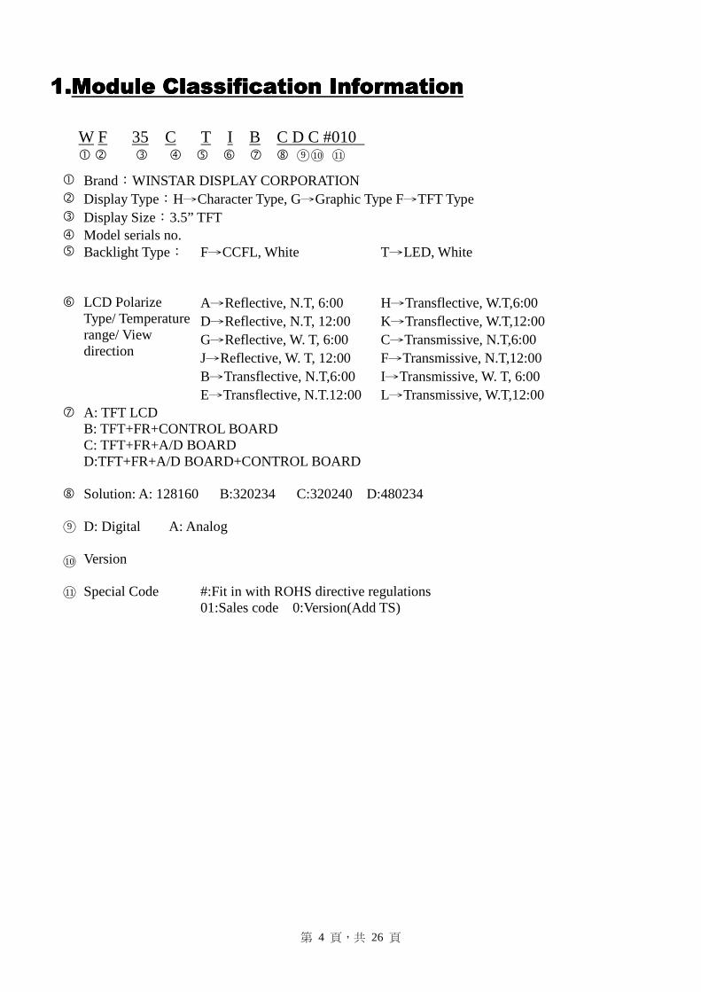
1111....Module Classification InformationModule Classification InformationModule Classification InformationModule Classification Information
W F 35 C T I B C D C #010 � � � � � � � � ○9 ○10 ○11
� Brand:WINSTAR DISPLAY CORPORATION � Display Type:H→Character Type, G→Graphic Type F→TFT Type � Display Size:3.5” TFT � Model serials no. � Backlight Type: F→CCFL, White
T→LED, White
� LCD Polarize
Type/ Temperature range/ View direction
A→Reflective, N.T, 6:00 D→Reflective, N.T, 12:00 G→Reflective, W. T, 6:00 J→Reflective, W. T, 12:00 B→Transflective, N.T,6:00 E→Transflective, N.T.12:00
H→Transflective, W.T,6:00 K→Transflective, W.T,12:00 C→Transmissive, N.T,6:00 F→Transmissive, N.T,12:00 I→Transmissive, W. T, 6:00 L→Transmissive, W.T,12:00
�
A: TFT LCD B: TFT+FR+CONTROL BOARD C: TFT+FR+A/D BOARD D:TFT+FR+A/D BOARD+CONTROL BOARD
� ○9 ○10
Solution: A: 128160 B:320234 C:320240 D:480234 D: Digital A: Analog Version
○11
Special Code #:Fit in with ROHS directive regulations 01:Sales code 0:Version(Add TS)

第 5 頁,共 26 頁
This product is composed of a TFT LCD panel, driver ICs, FPC, Control Board and a backlight unit. The following table described the features of WF35CTIBCDC#010
Item Dimension Unit
Dot Matrix 320 x RGBx240(TFT) dots
Module dimension 93.5 x 66.44 x 9.06 mm
View area 73.1x55.6 mm
Active area 70.08 x 52.56 mm
Dot size 0.073 x 0.219 mm
Driving IC package COG
LCD type TFT, Negative, Transmissive
View direction 6 o’clock
Backlight Type LED,Normally White
Controller IC SSD1963
*Expose the IC number blaze (Luminosity over than 1 cd) when using the LCM may cause IC operating
failure.
*Color tone slight changed by temperature and driving voltage.
第 6 頁,共 26 頁
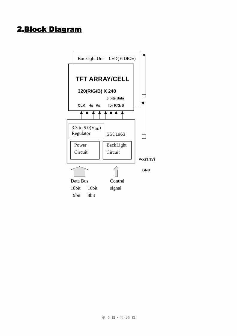
2222....Block DiagramBlock DiagramBlock DiagramBlock Diagram
TFT ARRAY/CELL
6 bits data
for R/G/B Hs Vs
Vcc(3.3V)
Backlight Unit LED( 6 DICE)
320(R/G/B) X 240
GND
SSD1963
Contral
signal
CLK
Data Bus
18bit 16bit
9bit 8bit
Power
Circuit
BackLight
Circuit
3.3 to 5.0(VDD) Regulator
第 7 頁,共 26 頁
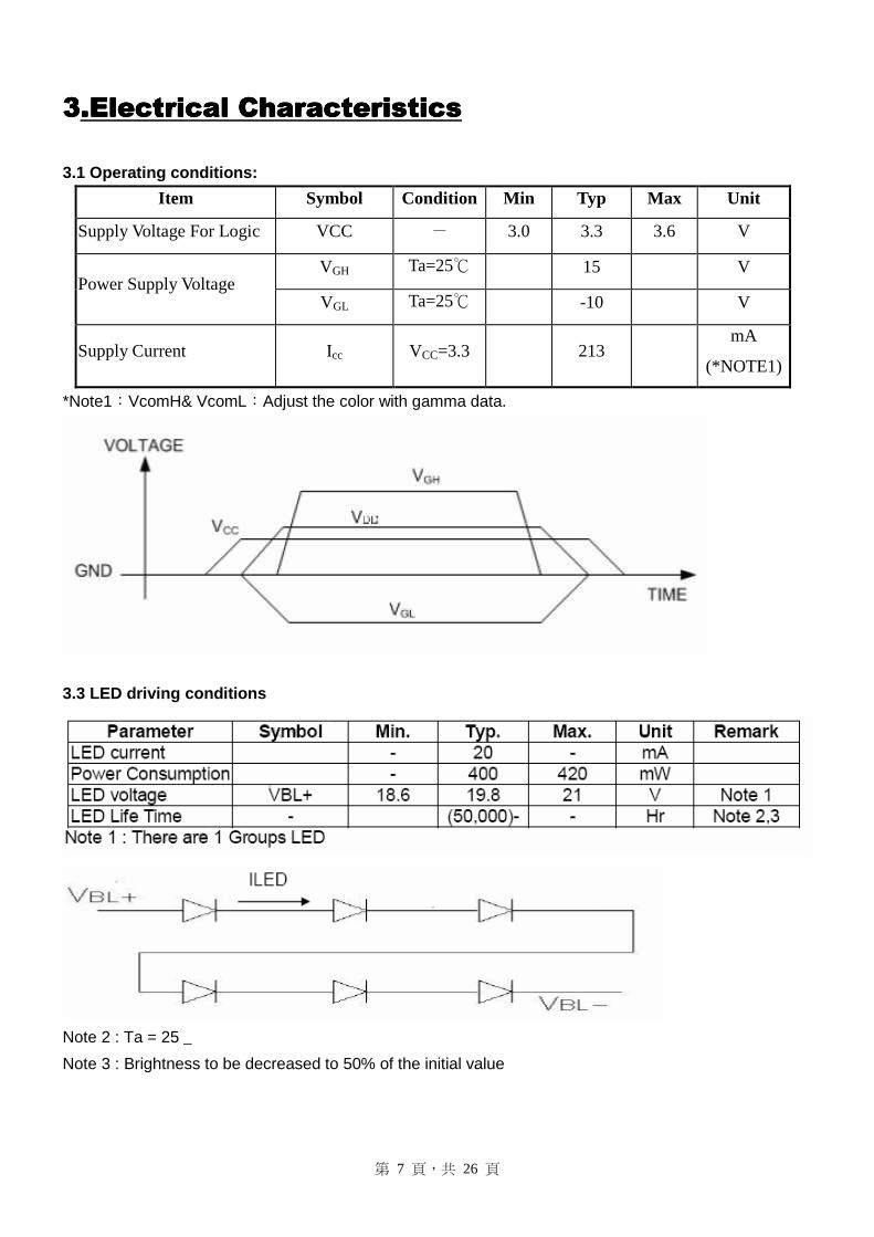
3333.Electrical Characteristics.Electrical Characteristics.Electrical Characteristics.Electrical Characteristics
3.1 Operating conditions:
Item Symbol Condition Min Typ Max Unit
Supply Voltage For Logic VCC - 3.0 3.3 3.6 V
VGH Ta=25℃ 15 V Power Supply Voltage
VGL Ta=25℃ -10 V
Supply Current Icc VCC=3.3 213 mA
(*NOTE1)
*Note1:VcomH& VcomL:Adjust the color with gamma data.
3.3 LED driving conditions
Note 2 : Ta = 25 _
Note 3 : Brightness to be decreased to 50% of the initial value

第 8 頁,共 26 頁
4444.Absolute Maximum Ratings.Absolute Maximum Ratings.Absolute Maximum Ratings.Absolute Maximum Ratings
Item Symbol Min Typ Max Unit
Operating Temperature TOP -20 - +70 ℃
Storage Temperature TST -30 - +80 ℃
VGH -0.3 - 32.0 V
VGL -22.0 - 0.3 V Power Voltage
VGH - VGL -0.3 - +45 V
Input voltage Vin -0.5 - 4.6 V
Logic output Voltage VOUT -0.5 - 4.6 V
Note: Device is subject to be damaged permanently if stresses beyond those absolute maximum
ratings listed above

第 9 頁,共 26 頁
5555.Interface Pin Function.Interface Pin Function.Interface Pin Function.Interface Pin Function
5.1 Pins Connection To Control Board P/N Symbol 16 BIT Function
1 VSS Ground 2 Vcc Power supply for Logic 3 BL_E Backlight control (H: On \ L: Off) 4 RS Command/Data select
5 WR 8080 family MPU interface : Write signal
6 RD 8080 family MPU interface: Read signal
7 DB0
8 DB1
9 DB2
10 DB3
11 DB4
12 DB5
13 DB6
14 DB7
15 DB8
16 DB9
17 DB10
18 DB11
19 DB12
20 DB13
21 DB14
22 DB15
Data bus
23 NC No connection
24 NC No connection 25 CS Chip select 26 RST REST
27 FGND Frame Gnd
28 NC No connection 29 NC No connection
30 NC No connection 31 NC No connection 32 NC No connection

第 10 頁,共 26 頁
6. DC 6. DC 6. DC 6. DC CharacteristicsCharacteristicsCharacteristicsCharacteristics
Conditions:
Voltage referenced to VSS
VDDD, VDDPLL = 1.2V
VDDIO, VDDLCD = 3.3V
TA = 25°C
DC Characteristics
Symbol Parameter Test Condition Min Typ Max Unit PSTY Quiescent Power 300 uW IIZ Input leakage
current -1 1 uA
IOZ Output leakage current
-1 1 uA
VOH Output high voltage
0.8VDDIO V
VOL Output low voltage
0.2VDDIO V
VIH Input high voltage
0.8VDDIO VDDIO + 0.5
V
VIL Input low voltage 0.2VDDIO V
第 11 頁,共 26 頁
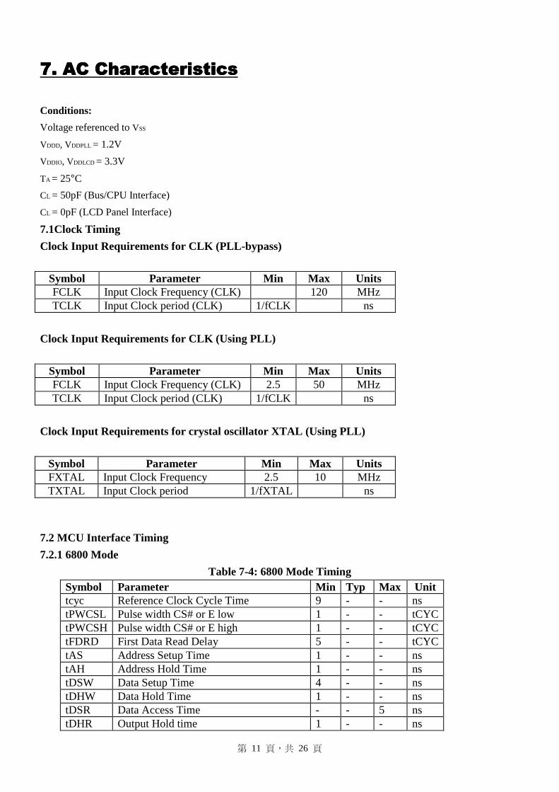
7. AC Characteristics7. AC Characteristics7. AC Characteristics7. AC Characteristics
Conditions:
Voltage referenced to VSS
VDDD, VDDPLL = 1.2V
VDDIO, VDDLCD = 3.3V
TA = 25°C
CL = 50pF (Bus/CPU Interface)
CL = 0pF (LCD Panel Interface)
7.1Clock Timing
Clock Input Requirements for CLK (PLL-bypass)
Symbol Parameter Min Max Units FCLK Input Clock Frequency (CLK) 120 MHz TCLK Input Clock period (CLK) 1/fCLK ns
Clock Input Requirements for CLK (Using PLL)
Symbol Parameter Min Max Units FCLK Input Clock Frequency (CLK) 2.5 50 MHz TCLK Input Clock period (CLK) 1/fCLK ns
Clock Input Requirements for crystal oscillator XTAL (Using PLL)
Symbol Parameter Min Max Units FXTAL Input Clock Frequency 2.5 10 MHz TXTAL Input Clock period 1/fXTAL ns
7.2 MCU Interface Timing
7.2.1 6800 Mode
Table 7-4: 6800 Mode Timing Symbol Parameter Min Typ Max Unit tcyc Reference Clock Cycle Time 9 - - ns tPWCSL Pulse width CS# or E low 1 - - tCYC tPWCSH Pulse width CS# or E high 1 - - tCYC tFDRD First Data Read Delay 5 - - tCYC tAS Address Setup Time 1 - - ns tAH Address Hold Time 1 - - ns tDSW Data Setup Time 4 - - ns tDHW Data Hold Time 1 - - ns tDSR Data Access Time - - 5 ns tDHR Output Hold time 1 - - ns
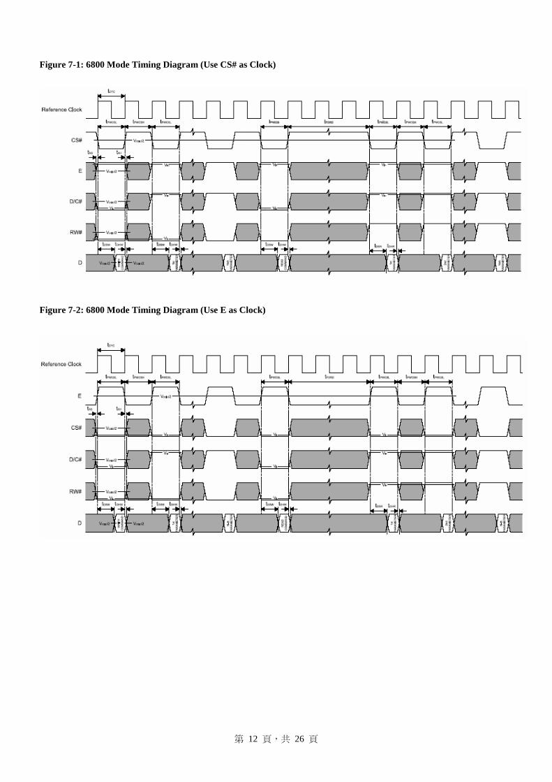
第 12 頁,共 26 頁
Figure 7-1: 6800 Mode Timing Diagram (Use CS# as Clock)
Figure 7-2: 6800 Mode Timing Diagram (Use E as Clock)

第 13 頁,共 26 頁
7.2.2 8080 Mode Write Cycle
Table 7-5: 8080 Mode Timing Symbol Parameter Min Typ Max Unit tcyc Reference Clock Cycle Time 9 - - ns tPWCSL Pulse width CS# low 1 - - tCYC tPWCSH Pulse width CS# high 1 - - tCYC tFDRD First Read Data Delay 5 - - tCYC tAS Address Setup Time 1 - - ns tAH Address Hold Time 1 - - ns tDSW Data Setup Time 4 - - ns tDHW Data Hold Time 1 - - ns tDSR Data Access Time - - 5 ns tDHR Output Hold time 1 - - ns Figure 7-3: 8080 Mode Timing Diagram

第 14 頁,共 26 頁
8888.... Data transfer order SettingData transfer order SettingData transfer order SettingData transfer order Setting
Pixel Data Format
Both 6800 and 8080 support 8-bit, 9-bit, 16-bit, 18-bit and 24-bit data bus. Depending on the width of the
data bus, the display data are packed into the data bus in different ways.
Pixel Data Format::::

第 15 頁,共 26 頁
9999 Register Depiction Register Depiction Register Depiction Register Depiction
Please consult the spec of SSD1963
第 16 頁,共 26 頁
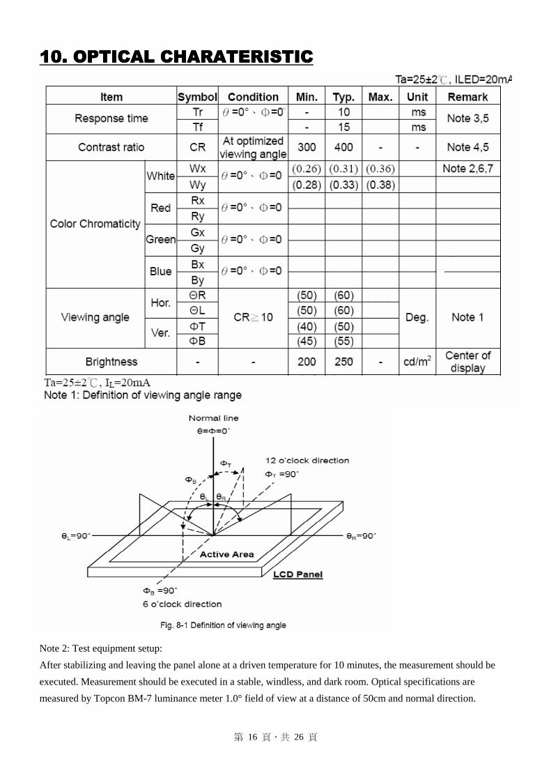
11110000. OPTICAL CHARATERISTIC. OPTICAL CHARATERISTIC. OPTICAL CHARATERISTIC. OPTICAL CHARATERISTIC
Note 2: Test equipment setup:
After stabilizing and leaving the panel alone at a driven temperature for 10 minutes, the measurement should be
executed. Measurement should be executed in a stable, windless, and dark room. Optical specifications are
measured by Topcon BM-7 luminance meter 1.0° field of view at a distance of 50cm and normal direction.

第 17 頁,共 26 頁
Note 3: Definition of Response time:
The response time is defined as the LCD optical switching time interval between “White” state and
“Black” state. Rise time, Tr, is the time between photo detector output intensity changed from
90﹪to 10﹪. And fall time, Tf, is the time between photo detector output intensity changed from10﹪to
90﹪.
Note 4: Definition of contrast ratio:
The contrast ratio is defined as the following expression.

第 18 頁,共 26 頁
Note 5: White Vi = Vi50 ± 1.5V
Black Vi = Vi50 ± 2.0V
“±” means that the analog input signal swings in phase with VCOM signal.
“±” means that the analog input signal swings out of phase with VCOM signal.
The 100% transmission is defined as the transmission of LCD panel when all the input terminals of
module are electrically opened.
Note 6: Definition of color chromaticity (CIE 1931)
Color coordinates measured at the center point of LCD
Note 7: Measured at the center area of the panel when all the input terminals of LCD panel are electrically
opened.
第 19 頁,共 26 頁
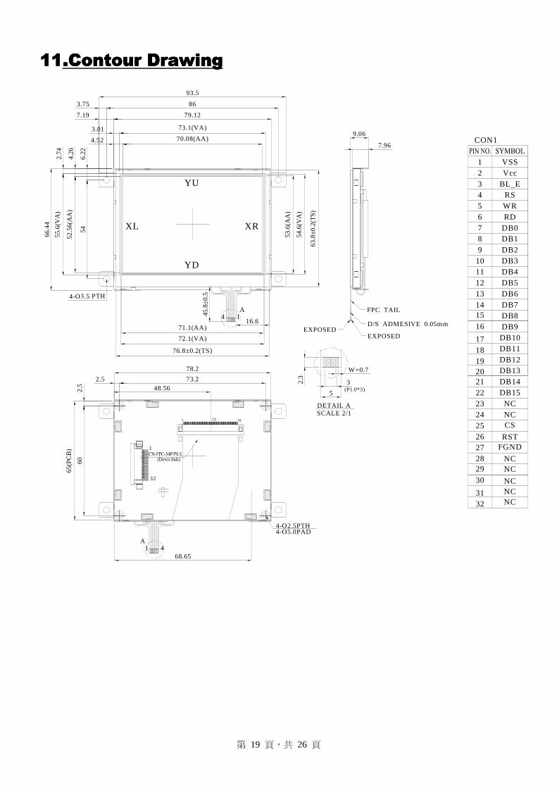
11111111....Contour DrawingContour DrawingContour DrawingContour Drawing
48.5673.2
78.2
2.5
60
65(P
CB
)
2.5
4-O5.0PAD4-O2.5PTH
68.65
J3
CON1
DB7DB6DB512
1413
VSS1
7
1110
89
4
65
32
RDWRRS
16
17
1920
18
15
VccBL_E
DB0DB1DB2DB3DB4
1
29
3231
30
2322
2425
21
2728
26
NC
NC
DB8DB9DB10DB11DB12DB13DB14DB15NCNCCS
RSTFGND
NC
NCNC
32
9.06
7.19
3.75
93.5
3.01
4.52
4-O3.5 PTH
66.4
4
73.1(VA)
6.22
54
86
70.08(AA)
79.12
52.5
6(A
A)
55.6
(VA
)
4.26
2.74
71.1(AA)
72.1(VA)
76.8±0.2(TS)
53.6
(AA
)
54.6
(VA
)
63.8
±0.2
(TS
)16.6
45.8
±0.5
2.3
DETAIL ASCALE 2/1
W=0.7
3(P1.0*3)
5
EXPOSEDEXPOSED
D/S ADMESIVE 0.05mm
FPC TAIL
YU
YD
XL XR
14A
7.96
1 4A
第 20 頁,共 26 頁
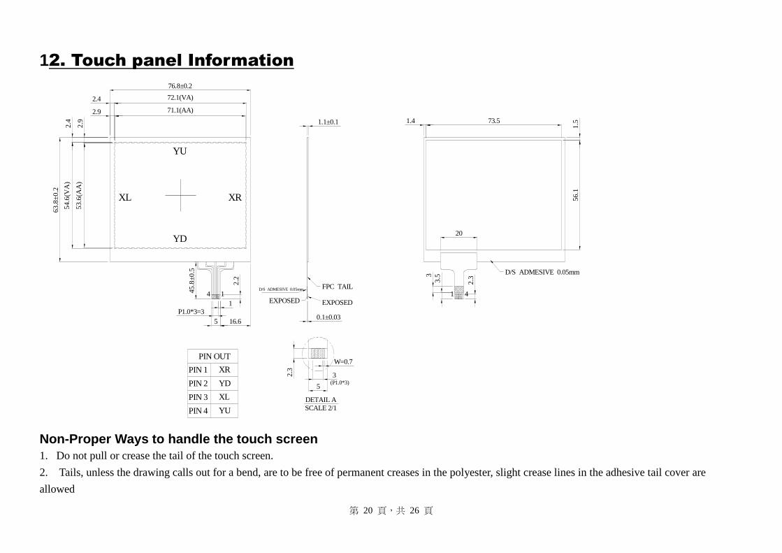
12. Touch panel Information
D/S ADMESIVE 0.05mm
PIN OUT
YD
XL
YU
PIN 2
PIN 4
PIN 3
PIN 1 XR
1.1±0.1
33.
5
56.1
1.573.51.4
20
0.1±0.03
2.2
P1.0*3=31
5 16.6
53.
6(A
A)
2.9
54.
6(V
A)
2.4
63.8
±0.2
71.1(AA)2.9
72.1(VA)2.4
76.8±0.2
1 42.
3
DETAIL ASCALE 2/1
W=0.7
3(P1.0*3)
5
EXPOSED
FPC TAIL
XRXL
YD
YU
4 145.8
±0.5
D/S ADMESIVE 0.05mm
EXPOSED
2.3
Non-Proper Ways to handle the touch screen
1. Do not pull or crease the tail of the touch screen.
2. Tails, unless the drawing calls out for a bend, are to be free of permanent creases in the polyester, slight crease lines in the adhesive tail cover are
allowed

第 21 頁,共 26 頁
13.Reliability
Test Item Test Condition
High Temperature Operation
70℃ for 240 hours
1hr 240hrs 1hr
70°C
20°C
High Temperature Operation Humidity Operation
60℃,90%RH for 240 hours
1hr 1hr
240 hrs
90%R.H60°C
20°C
Low Temperature Operation
-20℃ for 240hours
1hr. 240 hrs. 1hr.20°C
-20°C
High Temperature Storage
80℃ for 240 hours
1hr 240hrs 1hr
80°C
20°C
第 22 頁,共 26 頁
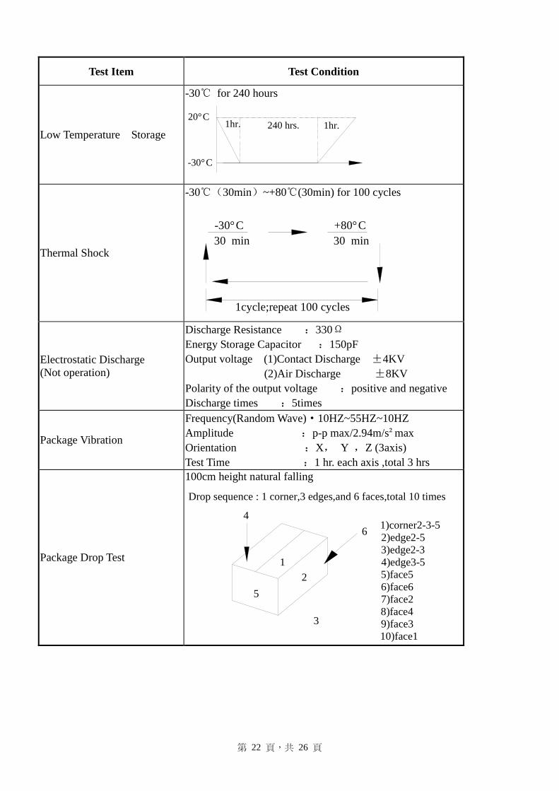
Test Item Test Condition
Low Temperature Storage
-30℃ for 240 hours
1hr. 240 hrs. 1hr.20°C
-30°C
Thermal Shock
-30℃(30min)~+80℃(30min) for 100 cycles
30 min 30 min
1cycle;repeat 100 cycles
-30°C +80°C
Electrostatic Discharge (Not operation)
Discharge Resistance :330Ω Energy Storage Capacitor :150pF Output voltage (1)Contact Discharge ±4KV (2)Air Discharge ±8KV Polarity of the output voltage :positive and negative Discharge times :5times
Package Vibration
Frequency(Random Wave)·10HZ~55HZ~10HZ Amplitude :p-p max/2.94m/s²max Orientation :X, Y ,Z (3axis) Test Time :1 hr. each axis ,total 3 hrs
Package Drop Test
100cm height natural falling
6
1
5
2
3
4
Drop sequence : 1 corner,3 edges,and 6 faces,total 10 times
1)corner2-3-52)edge2-53)edge2-34)edge3-55)face56)face67)face28)face49)face310)face1
第 23 頁,共 26 頁
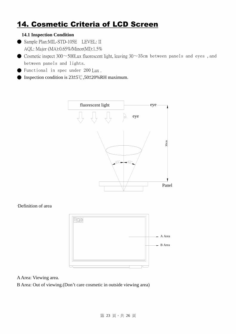
14. Cosmetic Criteria of LCD Screen
14.1 Inspection Condition ● Sample Plan:MIL-STD-105E LEVEL: II
AQL: Major (MA):0.65%/Minor(MI):1.5%
● Cosmetic inspect 300~500Lux fluorescent light, leaving 30~35cm between panels and eyes ,and
between panels and lights.
● Functional in spec under 200 Lux .
● Inspection condition is 23±5℃,50±20%RH maximum.
Panel
fluorescent light
eye
eye
30c
m
·Definition of area
A Area
B Area
A Area: Viewing area.
B Area: Out of viewing.(Don’t care cosmetic in outside viewing area)

第 24 頁,共 26 頁
14.2 Inspection specification
NO Item Acceptable specification Judgment
Criterion
1 Electrical Testing (MA)
1-1 sub pixel classification ● sub pixel: Number of sub pixel doesn’t exceed Five dot.
Sub Pixel(Dot)
a>Dark dot ----Four Allowed b>Bright dot---one Allowed c>The definition of dot ----The size of a defective dot over
1/2 of whole dot is regarded as one defective dot. d> Dark sub pixel: The distance more than 5mm between
dot and dot. e>Bright sub pixel: The distance more than 20mm between
bright dot and bright dot . ● Pixel : Three dots link together-----one allowed.
Pixel
1111----2Leakage to light 2Leakage to light 2Leakage to light 2Leakage to light
● Leakage to light be not allowed.
1111----3 Picture to sha3 Picture to sha3 Picture to sha3 Picture to shakekekeke
● Picture had shake ,twinkle and noise etc. instable of defect
that be not allowed.
1-4 Function
● No display or No function is not allowed.
● Source Line, Gate Line is not allowed.
● Contrast Ratio exceeds product specifications.
● Current consumption exceeds product specifications.
● Display malfunction.
N≤4 N≤1 N≤1 N=0 N=0 N=0
02 Mechanical
Dimension(MA)
2.1 Mechanical Dimension exceeds product specifications. 2-2 Out of frame and boss of plastic changed shape that be
not allowed.
N=0
第 25 頁,共 26 頁
NO Item Acceptable specification Judgment
Criterion
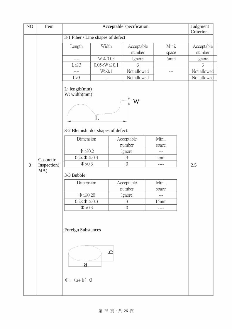
3 Cosmetic Inspection(MA)
3-1 Fiber / Line shapes of defect
L: length(mm) W: width(mm)
L
W
3-2 Blemish: dot shapes of defect.
3-3 Bubble
Foreign Substances
a
b
Φ=(a+ b)/2
Length Width Acceptable
number
Mini.
space
Acceptable
number
---- W≦0.05 lgnore lgnore
L≦3 0.05<W≦0.1 3
5mm
3
---- W>0.1 Not allowed Not allowed
L>3 ---- Not allowed
---
Not allowed
Dimension Acceptable
number
Mini.
space
Φ≦0.2 lgnore ---
0.2<Φ≦0.3 3 5mm
Φ>0.3 0 ----
Dimension Acceptable
number
Mini.
space
Φ≦0.20 lgnore ---
0.2<Φ≦0.3 3 15mm
Φ>0.3 0 ----
2.5

第 26 頁,共 26 頁
NO Item Acceptable specification Judgment
Criterion
3
Cosmetic Inspection(MA)
3-4 Scratch
● Impassive scratch as below.
3-5 Newton Ring
● D≦8mm----allowed
● D≧8mm----NG
Length Width Acceptable
number
Mini.
space
---- W≦0.05 lgnore
L≦3 0.05<W≦0.1 3
5mm
---- W>0.1 Not allowed
L>3 ---- Not allowed
---
4 Crack/Break(MA)
Not Allowed. N=0
5 Package
(MI)
5-1 Mixed product types
5-2 Shipping q’ty should be the same as “shipping notice form”
q’ty.
5-3 Outer box can’t broken .
N=0