Embed Size (px)
Citation preview

Company Confidential I 0506 CLEE 1 1
Where is the Packaging Technology Drifting? Choon Lee | EVP & CTO

Company Confidential I 0506 CLEE 2 2
Smartphone Market
39.2% 19.3% Growth Rate 6.2%
335 $ 314$ ASP 267$
2013 2014 2018
Source : IDC

Company Confidential I 0506 CLEE 3 3
History says (1)
< 1990s : Computing Era : Thermal fast memory Graphic performancene
Super BGA uBGA FCBGA
< 2014 : Smartphone Era : High density memory Formfactor Sensors
PoP WLCSP Low cost
> 2014 : Portable Era : Integration/Cost/Formfactor
Module/WLCSP/2.5D
Company Confidential I 0506 CLEE 4 4
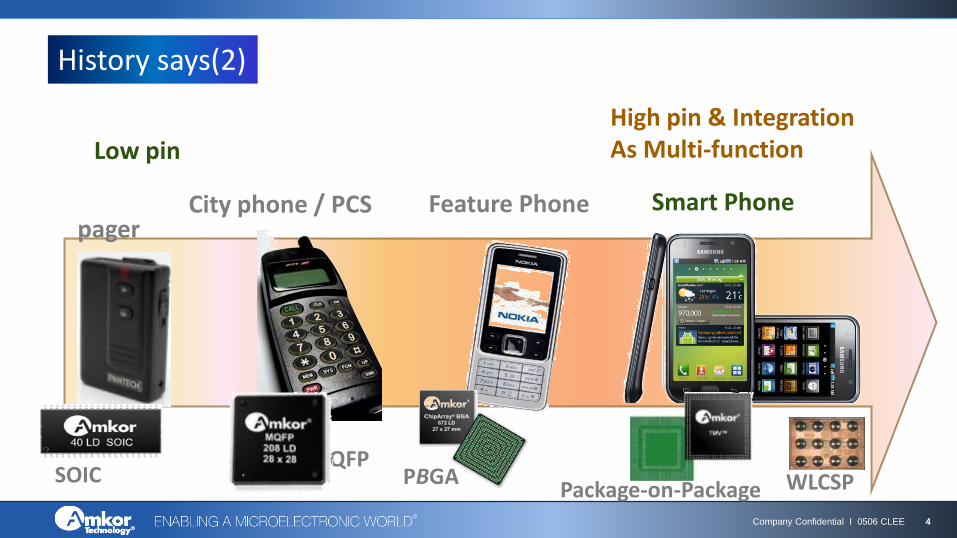
History says(2)
Package-on-Package WLCSP SOIC
Low pin High pin & Integration As Multi-function
pager City phone / PCS Feature Phone Smart Phone
QFP PBGA

Company Confidential I 0506 CLEE 5 5
New Trends in Package NFC WLCSP
MLF
MCU POP
fcCSP TSV
WiFi Bluetooth
LGA
Memory AP
Heartrate
MEMS Microphone
GPS
Inertial E-Compass
Min
iatu
riza
tio
n
Inte
grat
ion

Company Confidential I 0506 CLEE 6 6
Mobile Market Thin is IN: ergonomic form factor drives electronics
1.6 mm
1.3/1.4 mm
<1.0/0.8 mm
Memory package height:
Application processor package height:

Company Confidential I 0506 CLEE 7 7
Amkor Solutions to the Thin Trend
Max 0.91mm
0.28
0.10
0.05 0.15
0.16
0.10
4L Substrate
Option 1
Max 0.88mm
0.28
0.10
0.05 0.15
0.13
0.10
3L Coreless Substrate
Option 2
Option 3: Strip Grinding Chip attach (100um thickness die) 1st layer mold (150um mold)
Grinding (up to 30um die) 30um
0.1 mm ball

Company Confidential I 0506 CLEE 8 8
High End Smartphone Requires High Density Memory
Option 1 : Collaboration: Customer/Subcon J/Amkor
Disadvantage: Not lowest cost,
less fungible infrastructure
Upper Substrate
Base Substrate
Mold Resin Cu Core Solder Ball
Sn-3.0Ag-0.5Cu + Cu Core
Au Bump –Solder FC
Option 2 : Fan-in PoP version:
Advantage: cost optimized,
fungible infrastructure
Amkor’s eTMV
Interposer
Bond line
Company Confidential I 0506 CLEE 9 9
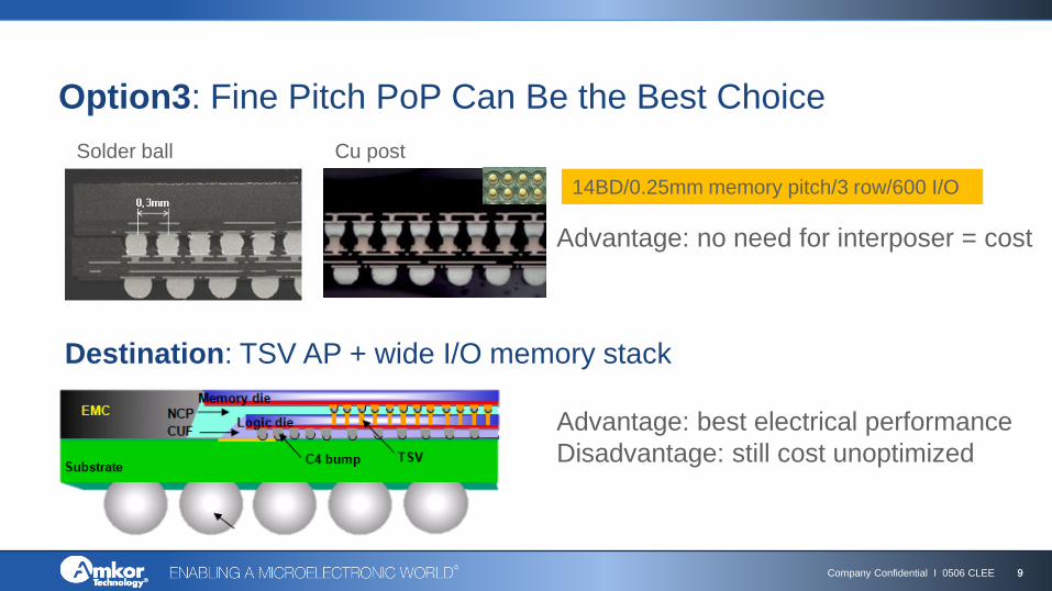
Solder ball
Option3: Fine Pitch PoP Can Be the Best Choice
Cu post
Destination: TSV AP + wide I/O memory stack
Advantage: no need for interposer = cost
14BD/0.25mm memory pitch/3 row/600 I/O
Advantage: best electrical performance
Disadvantage: still cost unoptimized

Company Confidential I 0506 CLEE 10 10
Low Cost Options for Low/Mid-End Smartphone
Clam : 27%
Materials : 73%
– Substrate = 54%
Option 1 : Bare Die PoP
Option 2: Flip Stack FCCSP
Option3: how to lower the subtrate cost
Flip Stack fcCSP Cost Structure
Company Confidential I 0506 CLEE 11 11
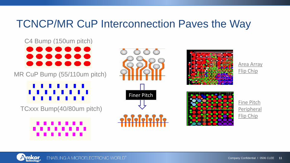
For the same # of bump
accommodation
Save 30% space
Save 50 % space
MR CuP Bump (55/110um pitch)
TCxxx Bump(40/80um pitch)
TCNCP/MR CuP Interconnection Paves the Way
C4 Bump (150um pitch)
Finer Pitch
Area Array Flip Chip
Fine Pitch Peripheral Flip Chip

Company Confidential I 0506 CLEE 12 12
4 layers
3 layers
Bump Layout and Density – Case Study 1 3 layer ETS conversion with fine pitch Cu Pillar
Device Name A B
Bump Pitch 150 50/100
Line/Space 25/25 20/20
PCB Layers 4 Layers (1-2-1) 3 Layers

Company Confidential I 0506 CLEE 13 13
Bump Layout and Density – Case Study 2 2 layer conversion with fine pitch Cu pillar
Device Name Solder Bump Cu Pillar
Bump Pitch 180 110/55
BPO / Pad size 80 / 105 25/100 /
CuBol
Line/Space 25/25 19/20
PCB Thickness 392 281
PCB Layers 4 Layers (1-2-1) 2 Layers
Body size 12 x 12 mm 12 x 12 mm
Reduced PCB Cost ratio% ref ~ -47%
4 layers
2 layers
Company Confidential I 0506 CLEE 14 14
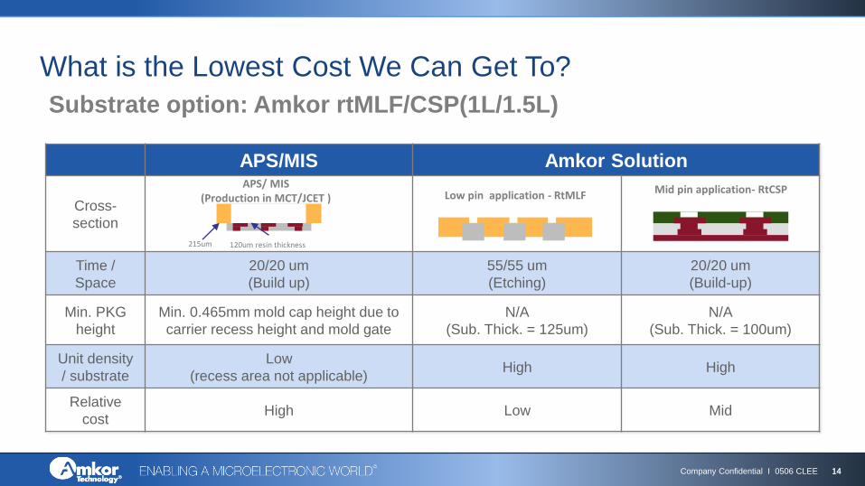
APS/MIS Amkor Solution
Cross-
section
Time /
Space
20/20 um
(Build up)
55/55 um
(Etching)
20/20 um
(Build-up)
Min. PKG
height
Min. 0.465mm mold cap height due to
carrier recess height and mold gate
N/A
(Sub. Thick. = 125um)
N/A
(Sub. Thick. = 100um)
Unit density
/ substrate
Low
(recess area not applicable) High High
Relative
cost High Low Mid
What is the Lowest Cost We Can Get To?
Substrate option: Amkor rtMLF/CSP(1L/1.5L)
Mid pin application- RtCSP APS/ MIS (Production in MCT/JCET )
120um resin thickness 215um
Low pin application - RtMLF

Company Confidential I 0506 CLEE 15 15
RtCSP – 14BD 0.8mm Pitch, 236LD: From 4L to 1L
4 L 1L
Bond finger pitch 0.103 0.120
Line/space 0.030/0.040 0.040/0.040 RtMLF is not feasible with current netlist
but possible when netlist is adjusted
Via count 283 N/A
Total wire length(0.7mil PCC) 540.737 663.19
Company Confidential I 0506 CLEE 16 16
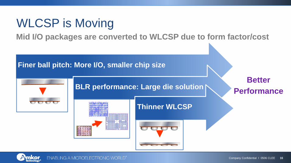
WLCSP is Moving Mid I/O packages are converted to WLCSP due to form factor/cost
Finer ball pitch: More I/O, smaller chip size
BLR performance: Large die solution Better
Performance
Thinner WLCSP

Company Confidential I 0506 CLEE 17 17
Current WLCSP Options
Cheapest solution : No RDL
Ni/Au (shown) UBM options
Molded layer WLCSP, CSPv
CSPn3
With 3 mask CSPnl
With 4 mask
BOR
With 2 mask

Company Confidential I 0506 CLEE 18 18
Large Die Solution: Form Factor/Cost
Silicon Metal Pad
Customer Passivation Polyimide 1
EMC
Plated Cu RDL
CSPv
12 x 12 rtCSP = 400 I/O
8 x 8 WLCSP = 400 I/O

Company Confidential I 0506 CLEE 19 19
Sensors In Smartphone and Tablet Are Expanding
– Inertial Sensors: Gyroscope, Accelerometer, Electronic compass (Magnetic sensor)
– Optical Sensors: Proximity, Ambient Light, *RGB Color, Image Sensors (Front/Rear camera)
– Touch Sensors: Multi-Touch, Pressure Touch
– Environmental Sensors: Temperature, Humidity, Barometric Pressure, CO Gas
– Wireless/RF Sensors: GPS, WiFi, Bluetooth, NFC
– Other Sensors: MEMS Microphones, Biometric/Fingerprint & BioSensors
: MEMS sensor
• ~18 sensors in Today’s Smartphones & Tablets

Company Confidential I 0506 CLEE 20 20
Electronics (Sensors) in Automobiles
Source: Clemson Vehicular Electronics Laboratory
Company Confidential I 0506 CLEE 21 21
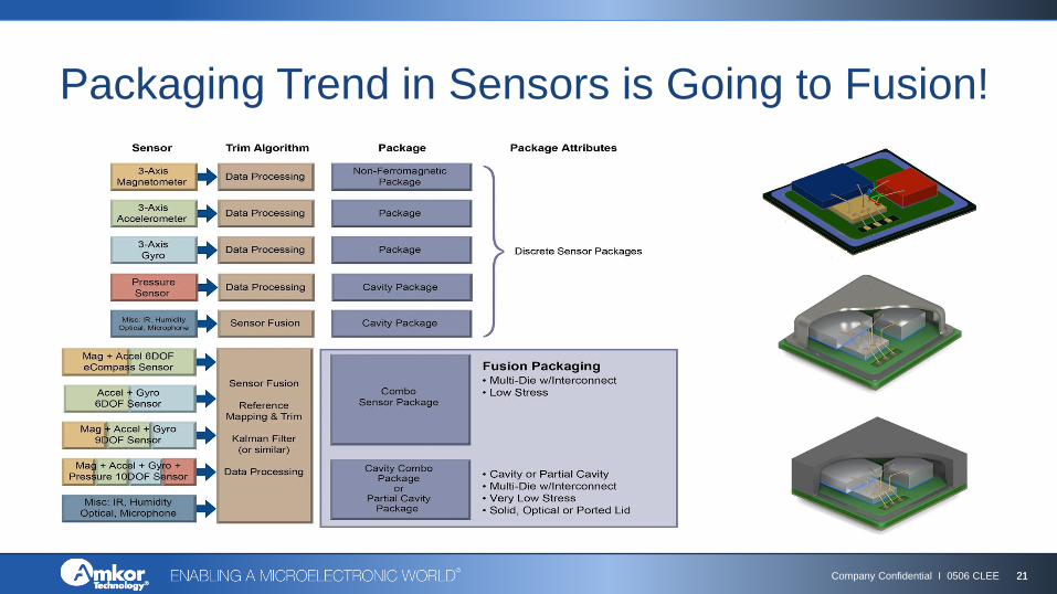
Packaging Trend in Sensors is Going to Fusion!

Company Confidential I 0506 CLEE 22 22
MEMS/Bio Sensor Package Platform Roadmap
Die Level Stress High Low
Low
Pa
cka
ge
Co
st
High
Overmolded
Dual, MLF and
CABGA
platforms
Exposed die
Film assisted
Dual, MLF and
CABGA
platforms
Strategic Platforms
Pre-mold cavity and lidded dual, MLF
and CABGA platforms
Ceramic package
platforms
Wafer level
Possum
FCCSP

Company Confidential I 0506 CLEE 23 23
High Density & Fast Memory is Required
2
4
8
16
32
Die
2012 2013 2014 Year 2015
16+1 die LGA & BGA
8+1 die LGA & BGA
4+1 die LGA & BGA
8+8 die
PoP
eMMC
LGA
Thin thickness
16 die Single
N5 N7
16+16 die PoP
16 die TSV
Company Confidential I 0506 CLEE 24 24
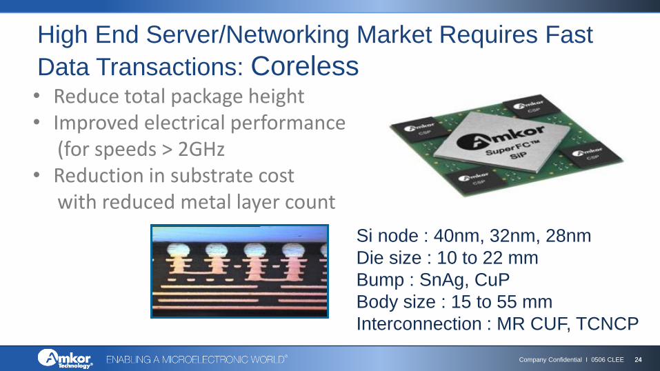
High End Server/Networking Market Requires Fast
Data Transactions: Coreless
Si node : 40nm, 32nm, 28nm
Die size : 10 to 22 mm
Bump : SnAg, CuP
Body size : 15 to 55 mm
Interconnection : MR CUF, TCNCP
• Reduce total package height • Improved electrical performance (for speeds > 2GHz • Reduction in substrate cost with reduced metal layer count

Company Confidential I 0506 CLEE 25 25
20 nm 26x25mm die
3477 BGA
14 L (6/2/6 build up)
CuP Area Array- MR CUF(Large Body/Die)
60x60/65x65mm body Cu Pillar FCBGA

Company Confidential I 0506 CLEE 26 26
TSV Market Projection
Next Time
MCM TSV
≤ 28nm (partition)
Markets:
Networking
Launched
Memory Cube
Markets:
Networking
Computing
2014
MCM TSV
- GPU + HBM
Markets:
Networking
Graphics
2015
MCM TSV
Logic + Logic/HBM
MCM WL-TSV
3D + SoC Partition
Markets:
Networking
Graphics, Mobile
2016
3D TSV
3D Logic-Logic
Markets:
Graphics
Mobile
Network
2017

Company Confidential I 0506 CLEE 27 27
2.5D Types Amkor Built
Customer A: 4 FPGA slices
Customer C: 1 Logic + 2 DRAMs
Customer D: Mech die + 2 Memories
Customer E: ASIC + 4 RLDRAMs
Customer B: 2 FPGA + 1 Tranciever
Amkor UTV : 2 logics + 4 memory
Heterogeneous Logic only
Logic and Memory

Company Confidential I 0506 CLEE 28 28
- Si interposer with TSV
- Si interposer without TSV
What is TSV-Less? Cost effective solution with no TSV
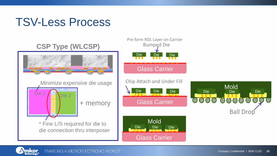
Company Confidential I 0506 CLEE 29 29
TSV-Less Process
CSP Type (WLCSP)
Die 1 Die 2
+ memory
Minimize expensive die usage
* Fine L/S required for die to
die connection thru interposer
Glass Carrier
Die Die
Pre form RDL Layer on Carrier Bumped Die
Die
Glass Carrier
Die Die Die
Chip Attach and Under Fill
Mold
Glass Carrier
Die Die Die
Mold Die Die Die
Ball Drop

Company Confidential I 0506 CLEE 30 30
How to Overcome Physical Barrier of Si: Si Photonics
Source : Intel website “50Gbps Si Photonics Link: Tech Overview”
Tranmitter module
Receiver module
Customer A : 2016 Customer B : 2015 Customer C : 2015 Customer D : 2015

Company Confidential I 0506 CLEE 31 31
Module with Imbedding +/- Paneling
Substrate
Passive
comp

Company Confidential I 0506 CLEE 32 32
PLP (Panel Level Package)
Pad interconection
Metal Plate
Die
Redistribution layer Adhesive
Solder Ball Resin
465um
This is the only avalible “panel” option in the packaging industry.

Company Confidential I 0506 CLEE 33 33
Extremely high UPH : chip shooter vs die bonder
12” wafer ~ 113sqin
18” x 24” panel ~ 432sqin
High density process : Panel

Company Confidential I 0506 CLEE 34 34
Big data Transference
New Hardware Concept
IOT
Gateway Things Decision
What is the New Driving Force ?

Company Confidential I 0506 CLEE 35 35
Google Module Phone
Company Confidential I 0506 CLEE 36 36
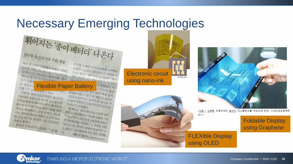
Necessary Emerging Technologies
Electronic circuit
using nano-ink
Foldable Display
using Graphene
FLEXIble Display
using OLED
Flexible Paper Battery