Embed Size (px)
Citation preview
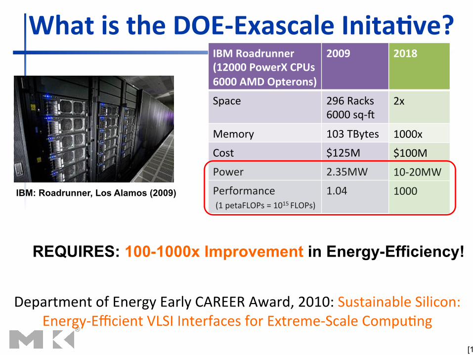
What is the DOE-‐Exascale Inita2ve? IBM Roadrunner (12000 PowerX CPUs 6000 AMD Opterons)
2018
Space 2x
1000 1000x
? $100M
10-‐20MW
1000
IBM Roadrunner (12000 PowerX CPUs 6000 AMD Opterons)
2009
Space 296 Racks 6000 sq-‐6
Memory 103 TBytes
Cost $125M
Power 2.35MW
Performance (1 petaFLOPs = 1015 FLOPs)
1.04 IBM: Roadrunner, Los Alamos (2009)
[1]
Department of Energy Early CAREER Award, 2010: Sustainable Silicon:
Energy-‐Efficient VLSI Interfaces for Extreme-‐Scale Compu[ng
REQUIRES: 100-1000x Improvement in Energy-Efficiency!
[2]
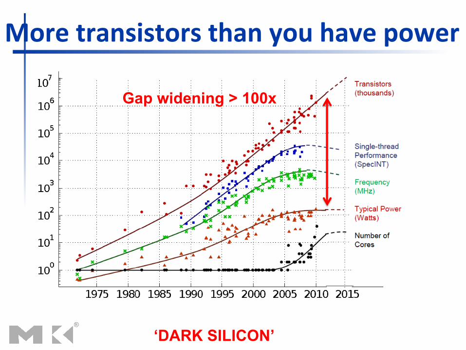
More transistors than you have power
Gap widening > 100x
‘DARK SILICON’
Chapter 4
The Processor

Chapter 4 — The Processor — 4
Introduction n CPU performance factors
n Instruction count n Determined by ISA and compiler
n CPI and Cycle time n Determined by CPU hardware
n We will examine two MIPS implementations n A simplified version n A more realistic pipelined version
n Simple subset, shows most aspects n Memory reference: lw, sw n Arithmetic/logical: add, sub, and, or, slt n Control transfer: beq, j
§4.1 Introduction
Chapter 4 — The Processor — 5
Instruction Execution n PC → instruction memory, fetch instruction
n Register numbers → register file, read registers
n Depending on instruction class n Use ALU to calculate
n Arithmetic result n Memory address for load/store n Branch target address
n Access data memory for load/store n PC ← target address or PC + 4

Chapter 4 — The Processor — 6
CPU Overview
Chapter 4 — The Processor — 7
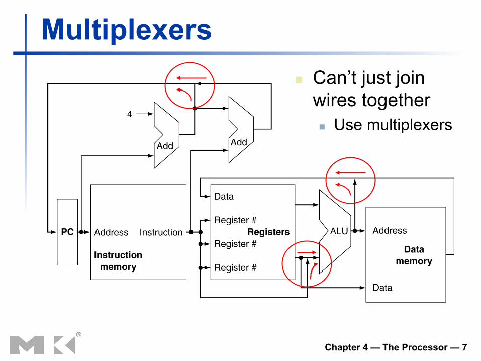
Multiplexers n Can’t just join
wires together n Use multiplexers
Chapter 4 — The Processor — 8
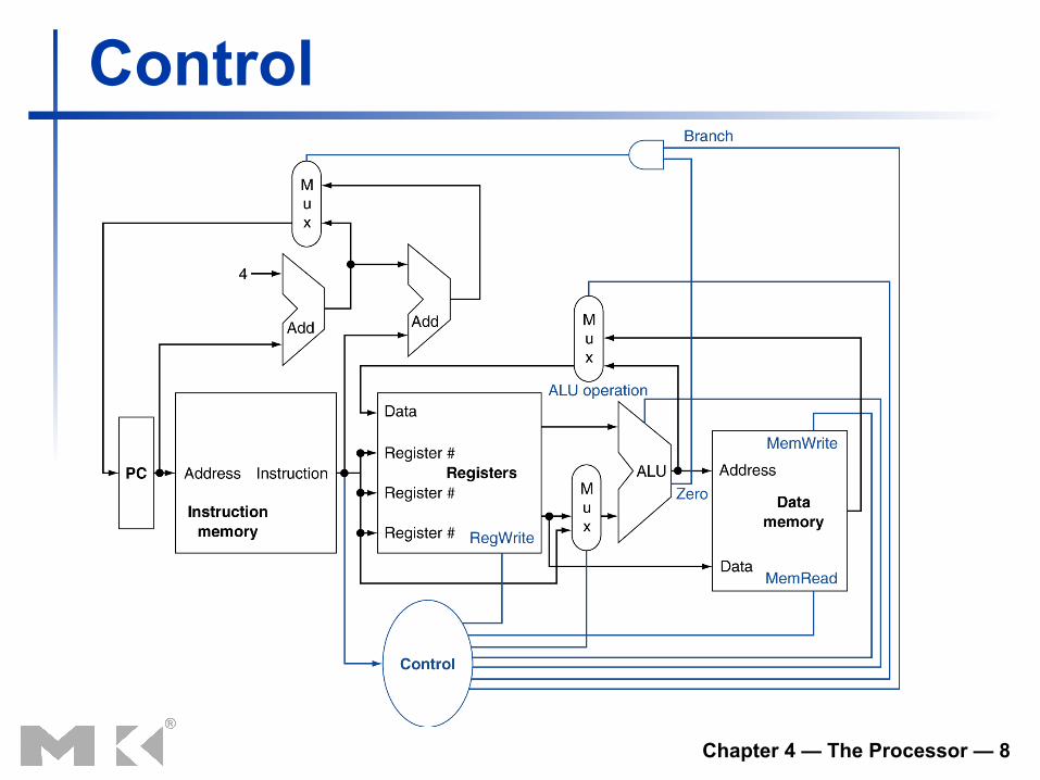
Control
Chapter 4 — The Processor — 9
Logic Design Basics §4.2 Logic D
esign Conventions
n Information encoded in binary n Low voltage = 0, High voltage = 1 n One wire per bit n Multi-bit data encoded on multi-wire buses
n Combinational element n Operate on data n Output is a function of input
n State (sequential) elements n Store information
Chapter 4 — The Processor — 10
Combinational Elements
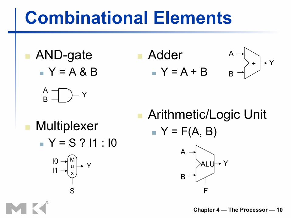
n AND-gate n Y = A & B A B Y
I0 I1 Y
M u x
S
n Multiplexer n Y = S ? I1 : I0
A
B Y +
A
B
Y ALU
F
n Adder n Y = A + B
n Arithmetic/Logic Unit n Y = F(A, B)

Chapter 4 — The Processor — 11
Sequential Elements n Register: stores data in a circuit
n Uses a clock signal to determine when to update the stored value
n Edge-triggered: update when Clk changes from 0 to 1
D
Clk
Q Clk
D
Q
Chapter 4 — The Processor — 12
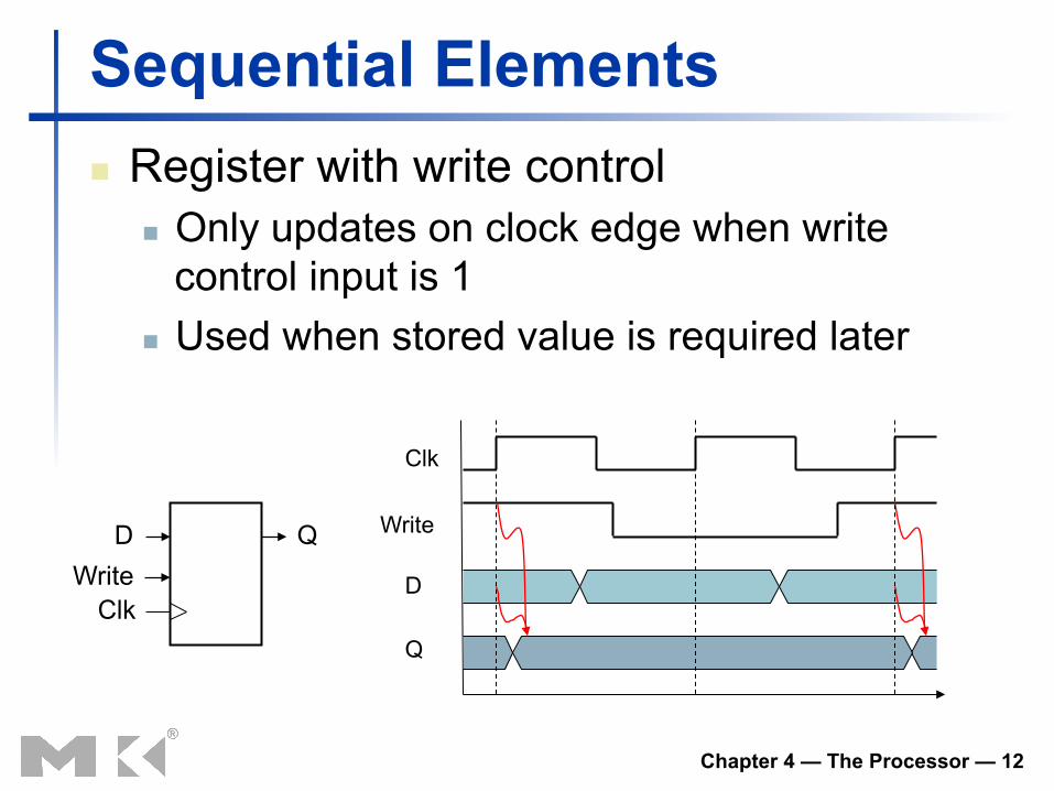
Sequential Elements n Register with write control
n Only updates on clock edge when write control input is 1
n Used when stored value is required later
D
Clk
Q Write
Write
D
Q
Clk
Chapter 4 — The Processor — 13
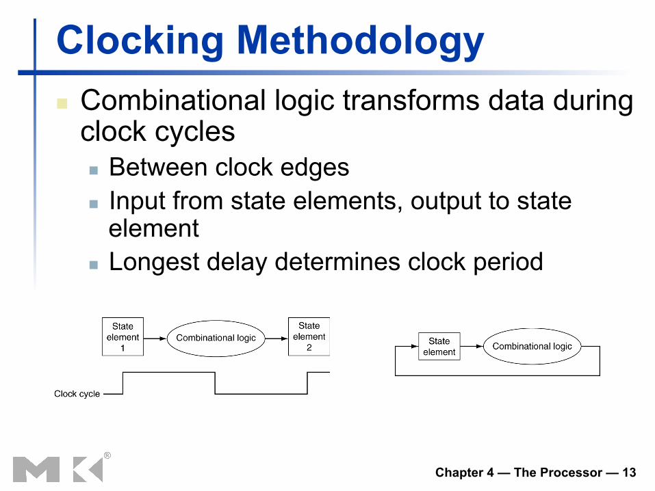
Clocking Methodology n Combinational logic transforms data during
clock cycles n Between clock edges n Input from state elements, output to state
element n Longest delay determines clock period
Chapter 4 — The Processor — 14
Building a Datapath n Datapath
n Elements that process data and addresses in the CPU
n Registers, ALUs, mux’s, memories, …
n We will build a MIPS datapath incrementally n Refining the overview design
§4.3 Building a D
atapath
Chapter 4 — The Processor — 15
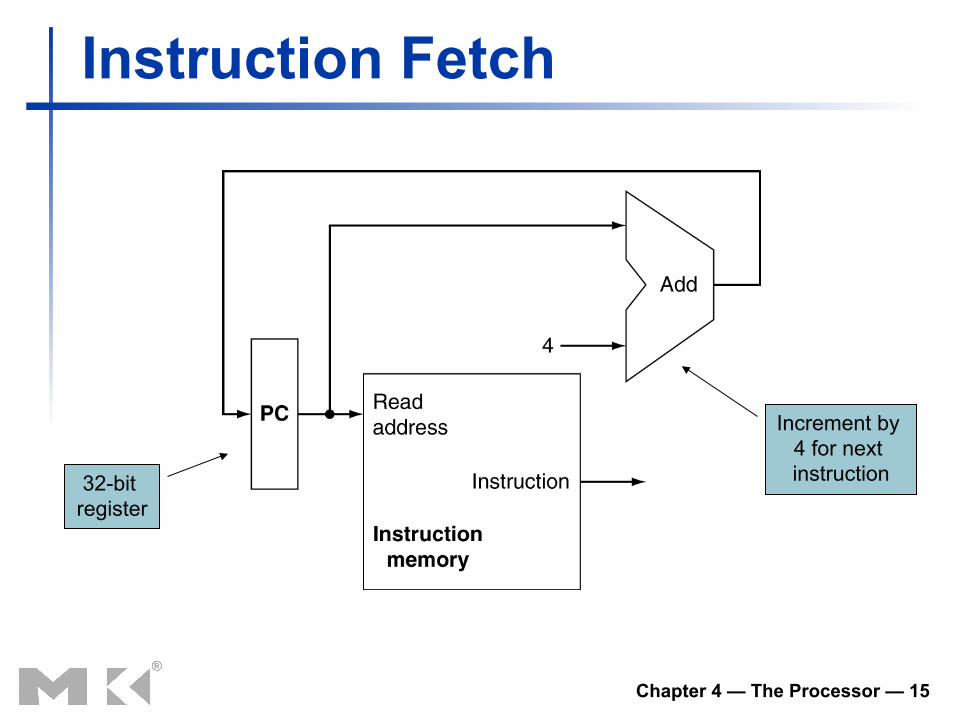
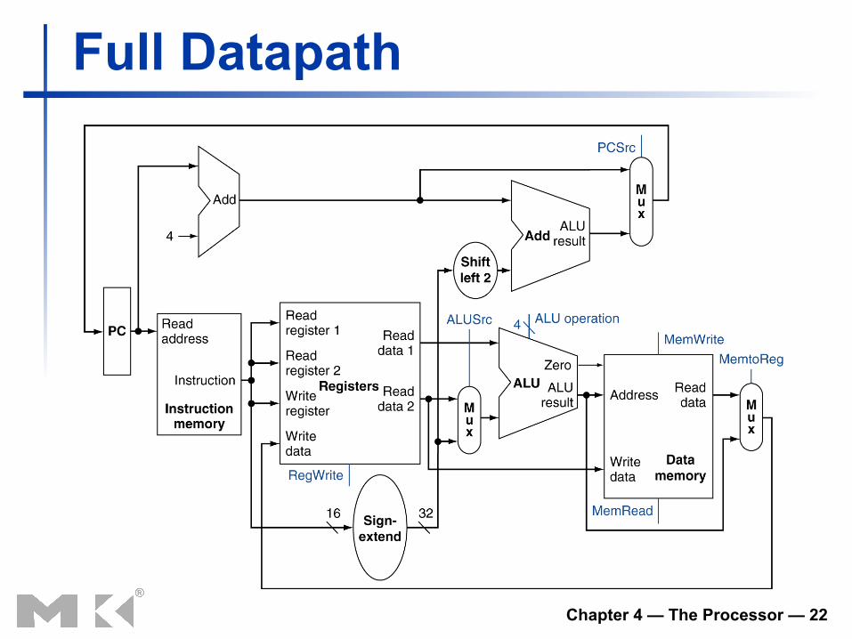
Instruction Fetch
32-bit register
Increment by 4 for next instruction
Chapter 4 — The Processor — 16
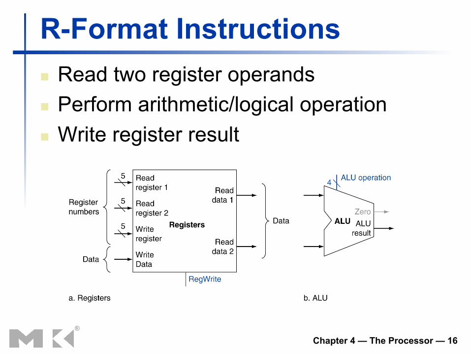
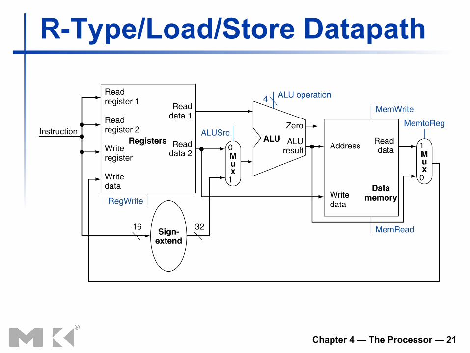
R-Format Instructions n Read two register operands n Perform arithmetic/logical operation n Write register result
Chapter 4 — The Processor — 17
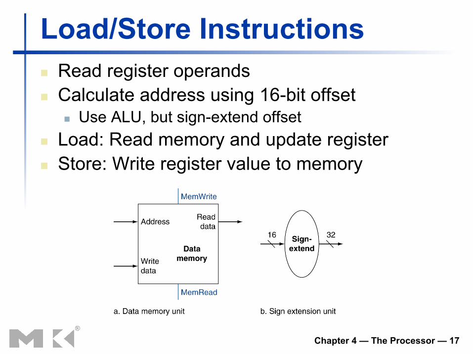
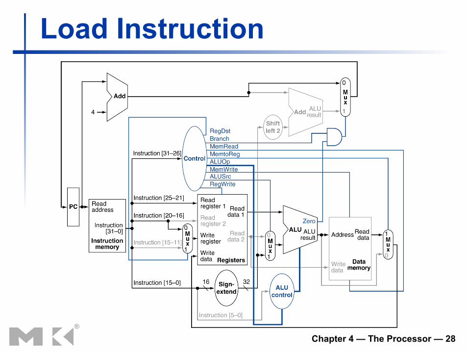
Load/Store Instructions n Read register operands n Calculate address using 16-bit offset
n Use ALU, but sign-extend offset n Load: Read memory and update register n Store: Write register value to memory
Chapter 4 — The Processor — 18
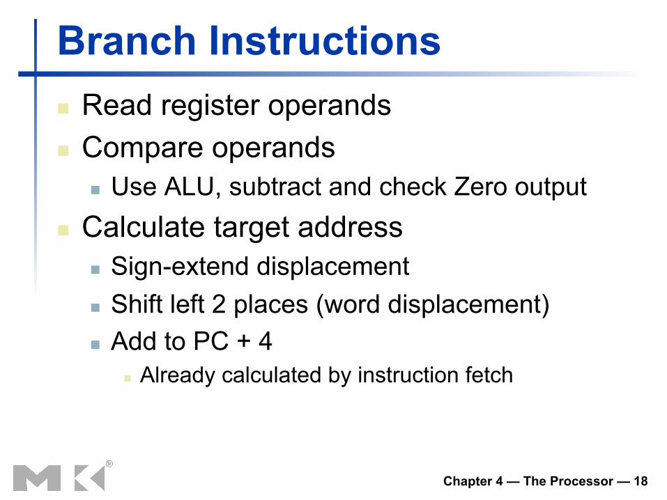
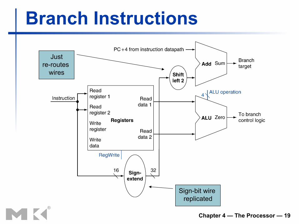
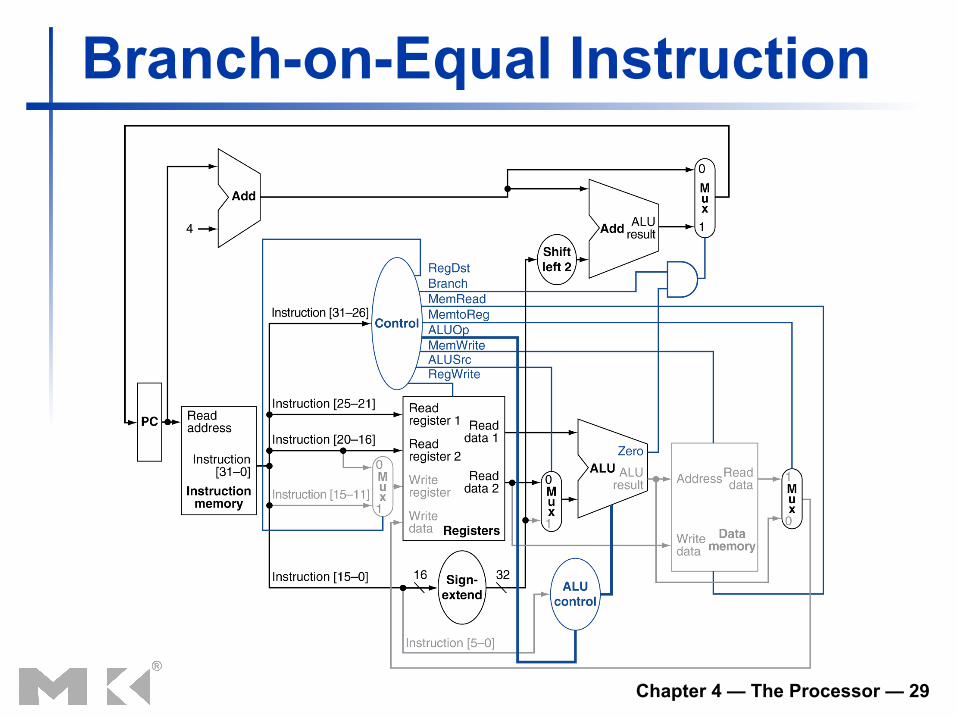
Branch Instructions n Read register operands n Compare operands
n Use ALU, subtract and check Zero output n Calculate target address
n Sign-extend displacement n Shift left 2 places (word displacement) n Add to PC + 4
n Already calculated by instruction fetch
Chapter 4 — The Processor — 19
Branch Instructions
Just re-routes
wires
Sign-bit wire replicated

Chapter 4 — The Processor — 20
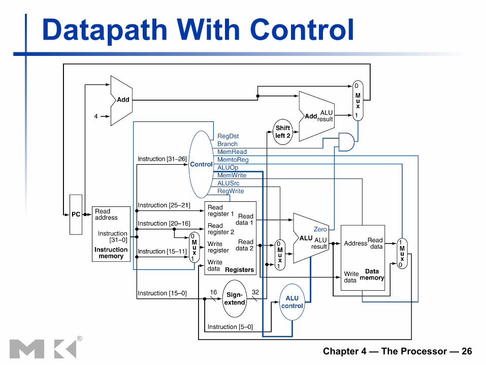
Composing the Elements n Data path does an instruction in one clock cycle
n Each datapath element can only do one function at a time
n Hence, we need separate instruction and data memories
n Use multiplexers where alternate data sources are used for different instructions
Chapter 4 — The Processor — 21
R-Type/Load/Store Datapath
Chapter 4 — The Processor — 22
Full Datapath
Chapter 4 — The Processor — 23
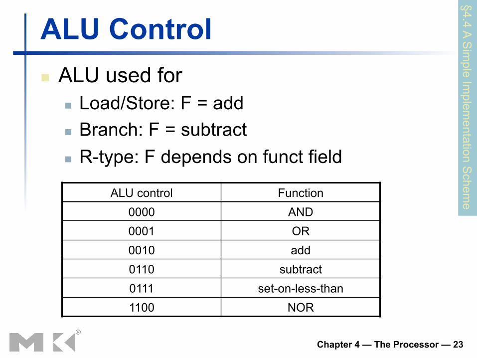
ALU Control n ALU used for
n Load/Store: F = add n Branch: F = subtract n R-type: F depends on funct field
§4.4 A Sim
ple Implem
entation Schem
e
ALU control Function 0000 AND 0001 OR 0010 add 0110 subtract 0111 set-on-less-than 1100 NOR
Chapter 4 — The Processor — 24
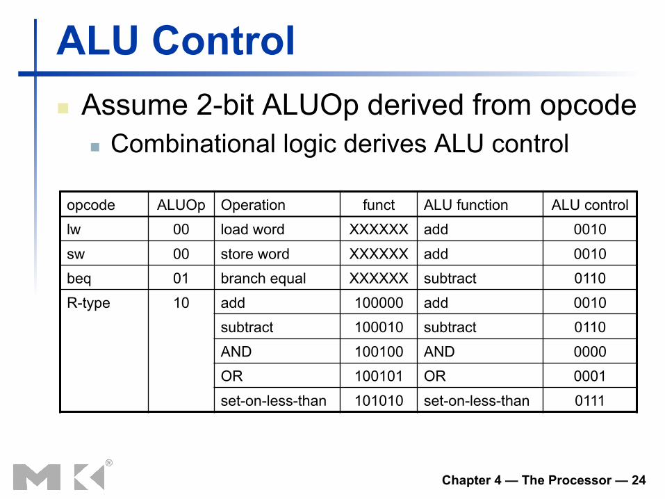
ALU Control n Assume 2-bit ALUOp derived from opcode
n Combinational logic derives ALU control
opcode ALUOp Operation funct ALU function ALU control lw 00 load word XXXXXX add 0010
sw 00 store word XXXXXX add 0010 beq 01 branch equal XXXXXX subtract 0110 R-type 10 add 100000 add 0010
subtract 100010 subtract 0110 AND 100100 AND 0000 OR 100101 OR 0001
set-on-less-than 101010 set-on-less-than 0111
Chapter 4 — The Processor — 25
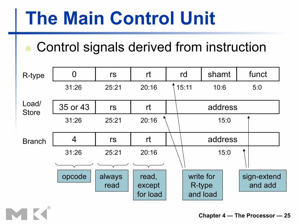
The Main Control Unit n Control signals derived from instruction
0 rs rt rd shamt funct 31:26 5:0 25:21 20:16 15:11 10:6
35 or 43 rs rt address 31:26 25:21 20:16 15:0
4 rs rt address 31:26 25:21 20:16 15:0
R-type
Load/ Store
Branch
opcode always read
read, except for load
write for R-type
and load
sign-extend and add
Chapter 4 — The Processor — 26
Datapath With Control

Chapter 4 — The Processor — 27
R-Type Instruction
Chapter 4 — The Processor — 28
Load Instruction
Chapter 4 — The Processor — 29
Branch-on-Equal Instruction
Chapter 4 — The Processor — 30
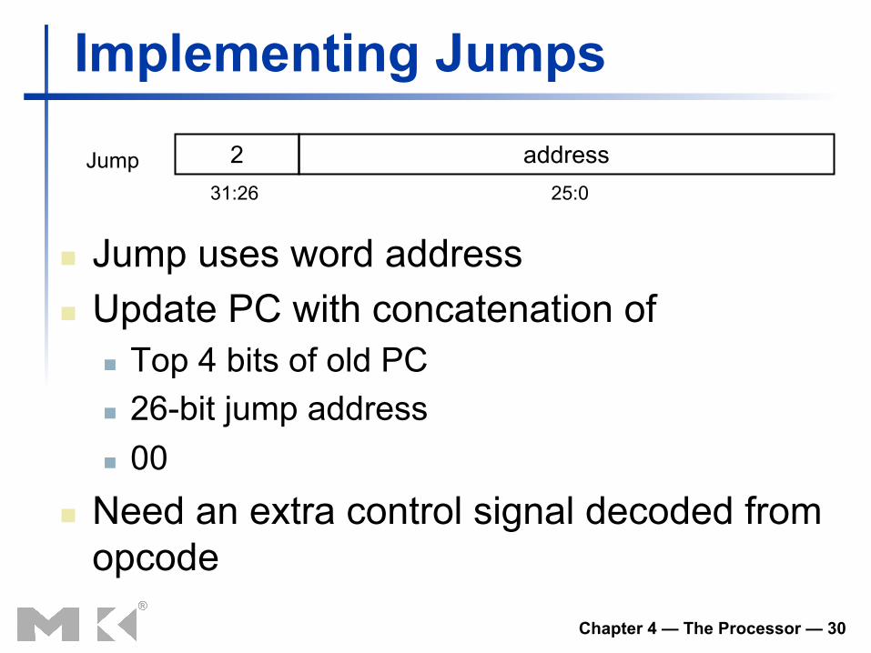
Implementing Jumps
n Jump uses word address n Update PC with concatenation of
n Top 4 bits of old PC n 26-bit jump address n 00
n Need an extra control signal decoded from opcode
2 address 31:26 25:0
Jump
Chapter 4 — The Processor — 31
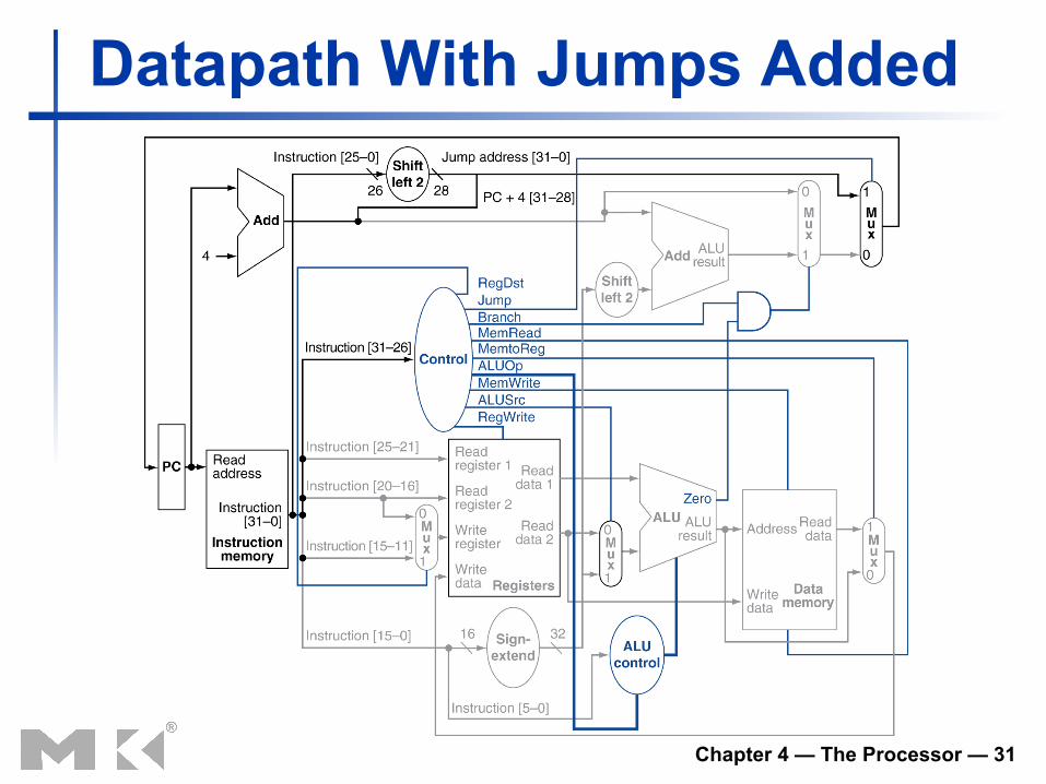
Datapath With Jumps Added
Chapter 4 — The Processor — 32
Performance Issues n Longest delay determines clock period
n Critical path: load instruction n Instruction memory → register file → ALU →
data memory → register file n Not feasible to vary period for different
instructions n Violates design principle
n Making the common case fast n We will improve performance by pipelining
Chapter 4 — The Processor — 33
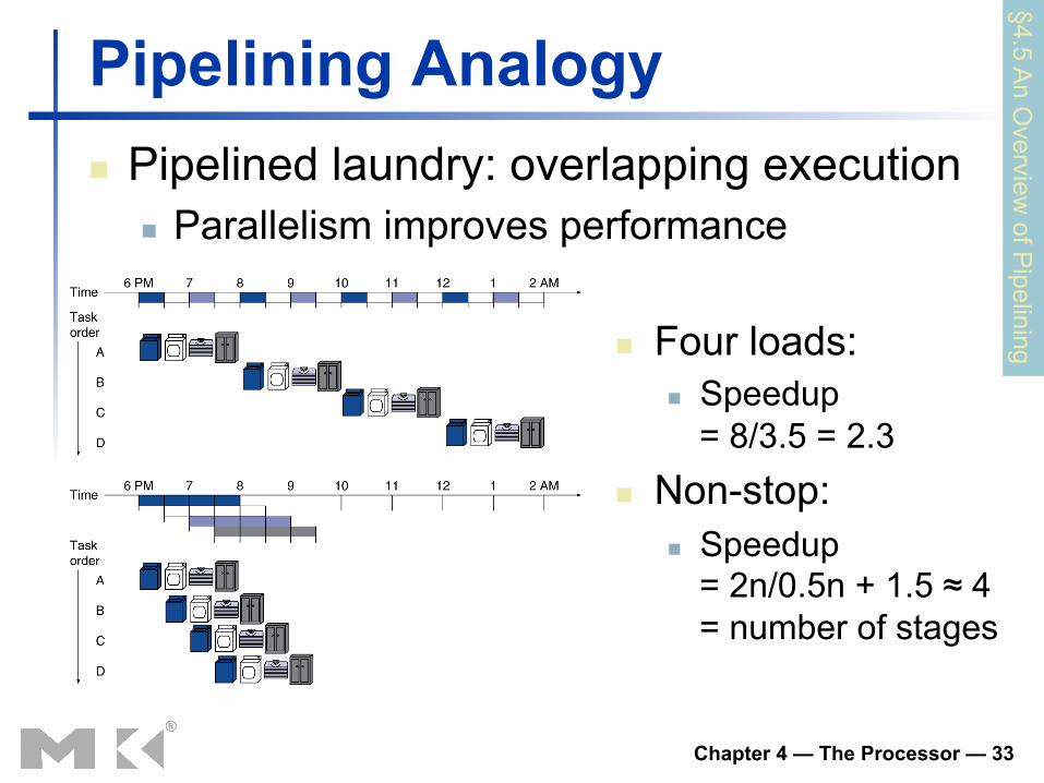
Pipelining Analogy n Pipelined laundry: overlapping execution
n Parallelism improves performance
§4.5 An O
verview of P
ipelining n Four loads: n Speedup
= 8/3.5 = 2.3 n Non-stop:
n Speedup = 2n/0.5n + 1.5 ≈ 4 = number of stages

Chapter 4 — The Processor — 34
MIPS Pipeline n Five stages, one step per stage
1. IF: Instruction fetch from memory 2. ID: Instruction decode & register read 3. EX: Execute operation or calculate address 4. MEM: Access memory operand 5. WB: Write result back to register