Embed Size (px)
Citation preview

- 1 -
INTRODUCTION TO COMPUTER & MICROPROCESSOR
What is a Computer?
A computer is an electronic machine that accepts information, stores it until the
information is needed, processes the information according to the instructions provided by the
user, and finally returns the results to the user. The computer can store and manipulate large
quantities of data at very high speed, but a computer cannot think. A computer makes decisions
based on simple comparisons such as one number being larger than another. Although the
computer can help solve a tremendous variety of problems, it is simply a machine. It cannot
solve problems on its own.
Computer Generations
From the 1950’s, the computer age took off in full force. The years since then have been
divided into periods or generations based on the technology used.
Generation Technology & Architecture Software & Applications Systems
First (1945‐54)
Vacuum tubes, Relay memories, CPU driven by PC and accumulator; fixed point Arithmetic
Machine & Assembly language, Single user Basic I/O using programmed and Internet mode.
ENIAC TIFRAC IBM 701 Princeton IAS
Second (1955‐64)
Discrete Transistors, Core Memories, Floating point, Arithmetic I/O, processors, Multiplexed memory access
HLL used with compilers, batch processing, Monitoring, Libraries
IBM7099
CDC 1604
Third (1965‐71)
Integrated circuits, Microprogramming, Pipelining, Caching, Lookahead Processing
Multiprogramming, Time sharing OS, Multi‐user applications
IBM 360/700 CDC 6000 TA‐ASC PDP‐8
Fourth (1971‐Present)
LSI/VLSI and Semiconductor memory, Microprocessors technology, Multiprocessors, vector super‐computing, multi computer
Multiprocessor OS, languages, Compilers
VAX 9800, Cray X‐MP, IBM 3600, Pentium Processor based systems (PCs), Ultra SPARC
Fifth (present & Beyond)
artificial intelligence and still in development,
parallel processing, superconductors, voice recognition Applications
Cray/MPP, TMC/CM‐5, Intel paragon, Fujitsu VP500
Table (1.1): Generations of computer

- 2 -
Types of Computers
Computer now comes in a variety of shapes and sizes, which could be roughly classified
according to their processing power into five sizes: super large, large, medium, small, and tiny.
Microcomputers are the type of computers that we are most likely to notice and use in our
everyday life. In fact there are other types of computers that you may use directly or indirectly:
Supercomputers‐super large computers: supercomputers are high‐ capacity machines
with hundreds of thousands of processors that can perform more than 1 trillion
calculations per second. These are the most expensive but fastest computers available.
"Supers," as they are called, have been used for tasks requiring the processing of
enormous volumes of data, such as doing the U.S. census count, forecasting weather,
designing aircraft, modeling molecules, breaking codes, and simulating explosion of
nuclear bombs.
Mainframe computers ‐ large computers: The only type of computer available
until the late 1960s, mainframes are water‐ or air‐cooled computers that vary in size
from small, to medium, to large, depending on their use. Small mainframes are often
called midsize computers; they used to be called minicomputers. Mainframes are used
by large organizations such as banks, airlines, insurance companies, and colleges‐for
processing millions of transactions. Often users access a mainframe using a terminal,
which has a display screen and a keyboard and can input and output data but cannot by
itself process data.
Workstations ‐ medium computer: Introduced in the early 1980s, workstations, are
expensive, powerful computers usually used for complex scientific, mathematical, and
engineering calculations and for computer‐aided design and computer‐aided
manufacturing. Providing many capabilities comparable to midsize mainframes,
workstations are used for such tasks as designing airplane fuselages, prescription drugs,
and movie special effects. Workstations have caught the eye of the public mainly for
their graphics capabilities, which are used to breathe three‐dimensional life into movies
such as Jurassic Park and Titanic. The capabilities of low‐end workstations overlap those
of high‐end desktop microcomputers.

- 3 -
Microcomputer ‐ small computers: Microcomputers, also called personal computers (PC),
can fit next to a desk or on a desktop, or can be carried around. They are either stand‐
alone machines or are connected to a computer network, such as a local area network. A
local area network (LAN) connects, usually by special cable, a group of desktop PCs and
other devices, such as printers, in an office or a building. Microcomputers are of several
types:
Desktop PCs: are those in which the case or main housing sits on a desk, with
keyboard in front and monitor (screen) often on top.
Tower PCs: are those Microcomputer in which the case sits as a "tower," often on the
floor beside a desk, thus freeing up desk surface space.
Laptop computers (also called notebook computers): are lightweight portable
computers with built‐in monitor, keyboard, hard‐disk drive, battery, and AC adapter
that can be plugged into an electrical outlet; they weigh anywhere from 1.8 to 9
pounds.
Personal digital assistants (PDAs) (also called handheld computers or palmtops)
combine personal organization tools‐schedule planners, address books, to‐do lists.
Some are able to send e‐mail and faxes. Some PDAs have touch‐sensitive screens. Some
also connect to desktop computers for sending or receiving information.
Microcontrollers‐tiny computers: Microcontrollers, also called embedded computers,
are the tiny, specialized microprocessors installed in "smart" appliances and
automobiles. These microcontrollers enable PDAs microwave ovens, for example, to
store data about how long to cook your potatoes and at what temperature.
Basic Blocks of a Microcomputer
All Microcomputers consist of (at least):
1. Microprocessor Unit (MPU) MPU is the brain of microcomputer
2. Program Memory (ROM)
3. Data Memory (RAM)
4. Input / Output ports
5. Bus System
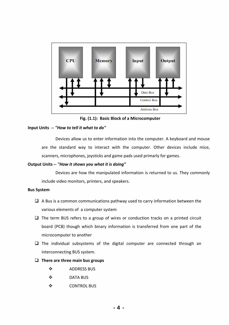
- 4 -
Input Units ‐‐ "How to tell it what to do"
Devices allow us to enter information into the computer. A keyboard and mouse
are the standard way to interact with the computer. Other devices include mice,
scanners, microphones, joysticks and game pads used primarly for games.
Output Units ‐‐ "How it shows you what it is doing"
Devices are how the manipulated information is returned to us. They commonly
include video monitors, printers, and speakers.
Bus System A Bus is a common communications pathway used to carry information between the
various elements of a computer system
The term BUS refers to a group of wires or conduction tracks on a printed circuit
board (PCB) though which binary information is transferred from one part of the
microcomputer to another
The individual subsystems of the digital computer are connected through an
interconnecting BUS system.
There are three main bus groups
ADDRESS BUS
DATA BUS
CONTROL BUS
Fig. (1.1): Basic Block of a Microcomputer

- 5 -
Data Bus The data bus consists of 8, 16, or 32 parallel signal lines. As indicated by the double‐
ended arrows on the data bus line in Figure (1.1), the data bus lines are bidirectional. This
means that the CPU can read data in from memory or from a port on these lines, or it can
send data out to memory or to a port on these lines. Many devices in a system will have
their outputs connected to the data bus, but only one device at a time will have its outputs
enabled. Any device connected on the data bus must have three‐state outputs so that its
outputs can be disabled when it is not being used to put data on the bus.
Address Bus
The address bus consists of 16, 20, 24, or 32 parallel signal lines. On these lines the CPU
sends out the address of the memory location that is to be written to or read from. The number
of memory locations that the CPU can address is determined by the number of address lines. If
the CPU has N address lines, then it can directly address 2N memory locations. For example, a
CPU with 16 address lines can address 216 or 65,536 memory locations, a CPU with 20 address
lines can address 220 or 1,048,576 locations. When the CPU reads data from or writes data to a
port, it sends the port address out on the address bus.
Control Bus
The control bus consists of 4 to 10 parallel signal lines. The CPU sends out signals on
the control bus to enable the outputs of addressed memory devices or port devices. Typical
control bus signals are Memory Read, Memory Write, I/O Read, and l/O Write.
Main memory The memory section usually consists of a mixture of RAM (Random Access Memory) and
ROM (Read Only Memory). It may also have magnetic floppy disks, magnetic hard disks, or
optical disks (CDs, DVDs).
The duties of the memory are :
To store programs
To provide data to the MPU on request
To accept result from the MPU for storage

- 6 -
Main memory Types
ROM : read only memory. Contains program (Firmware). does not lose its
contents when power is removed (Non‐volatile)
RAM: random access memory (read/write memory) used as variable data,
loses contents when power is removed volatile. When power up will contain
random data values
Central Processing Unit (Microprocessor)
The central processing unit or CPU controls the operation of the computer. In a
computer the CPU is a microprocessor. The CPU controls the operation of the computer.
The CPU fetches binary‐coded instructions from memory, decodes the instructions into a
series of simple actions, and carries out these actions in a sequence of steps. The CPU also
contains an address counter or instruction pointer register, which holds the address of the
next instruction or data item to be fetched from memory; general‐purpose registers, which
are used for temporary storage of binary data; and circuitry, which generates the control
bus signals.
Evaluation of the Microprocessors
The evolution of microprocessors has been known to follow Moore's Law when it comes
to steadily increasing performance over the years. This law suggests that the complexity of an
integrated circuit, with respect to minimum component cost, doubles every 18 months. This
dictum has generally proven true since the early 1970s. From their humble beginnings as the
drivers for calculators, the continued increase in power has led to the dominance of
microprocessors over every other form of computer; every system from the largest mainframes
to the smallest handheld computers now uses a microprocessor at its core.
Motorola and Intel have invented most of the microprocessors over the last decade.
Table (1.2) lists some of types that belong to these companies (families) of microprocessors.
Table (1.2): Some Types of Microprocessors

- 7 -
Company 4 bit 8 bit 16 bit 32 bit 64 bit
Intel 4004 4040
8008 8080 8085
8088/6 80186 80286
80386 80486
80860 Pentium
Zilog Z80 Z8000 Z8001 Z8002
Motorola 6800 6802 6809
68006 68008 68010
68020 68030 68040
The Microprocessor‐Based Personal Computer System
Figure (1.2) shows the block diagram of the personal computer. The block diagram is
composed of four parts:
1. Bus Architecture:‐ Three buses:
Address
Data
Control:
Fig. (1.2): The block diagram of the personal computer

- 8 -
2. The memory
The memory structures of all Intel 80X86‐Pentium 4 personal computer systems are
similar. This includes the first personal computers based upon the 8088 introduced in 1981 by
IBM to the most powerful high‐speed versions of today based on the Pentium 4. Figure (1.4)
illustrates the memory map of a personal computer system.
The memory system is divided into three main parts: TPA (Transient Program Area), system area,
and XMS (Extended Memory System). The type of microprocessor in your computer determines
whether an extended memory system exists. If the computer is based upon an older 8086 or
8088 (a PC or XT), the TPA and system areas exist, but there is no extended memory area. The PC
and XT contain 640K bytes of TPA and 384K bytes of system memory, for a total memory size of
IM bytes. We often call the first 1M byte of memory the real or conventional memory system
because each Intel microprocessor is designed to function in this area by using its real mode of
operation.
Computer systems based on the 80286 through the Pentium 4 not only contain the TPA
(640K bytes) and system area (384K bytes), they also contain extended memory. These machines
are often called AT class machines.
The TPA: The transient program area (TPA) holds the DOS operating system and other programs
that control the computer system. The TPA also stores DOS application programs. The length of
the TPA is 640K bytes. Figure (1‐5) shows the memory map of the TPA.
Fig. (1.3): The block diagram of computer system showing the buses structure

- 9 -
The System Area: The system area contains program on rather a ROM or flash memory, and
areas of RAM for data storage. Figure (1‐6) shows the memory map of the system area.
3. I/O System
The I/O devices allow the microprocessor to
communicate between itself and the outside world. The I/O
space in a computer system extends from port 0000H to port
FFFFH. The I/O space allows the computer to access up to 64k
different 8‐bit I/O devices. Figure (1‐7) shows the I/O map
found in many personal computer systems.
The I/O area contains two major sections. The area
below I/O location 0400H is considered reserved for system
devices. The remaining area is available I/O space for expansion
on newer devices.
Fig. (1.7): The I/O map of a PC
Fig. (1.4): The memory map
of the PC Fig. (1.5): The memory map of
the TPA area of a PC Fig. (1.6): The system area of a
typical PC
- 10 -
8086 Microprocessor
The main features of 8086 µp are:
It is a 16‐bit Microprocessor (μp). It’s ALU, internal registers works with 16bit binary word.
8086 has a 20 bit address bus can access up to 220= 1 MB memory locations.
8086 has a 16bit data bus. It can read or write data to a memory/port either 16bits or 8 bit
at a time.
It can support up to 64K I/O ports.
It provides 14, 16 ‐bit registers.
Frequency range of 8086 is 6‐10 MHz
It has multiplexed address and data bus AD0‐ AD15 and A16 – A19.
It requires single phase clock with 33% duty cycle to provide internal timing.
It can prefetch up to 6 instruction bytes from memory and queues them in order to speed
up instruction execution.
It requires +5V power supply.
A 40 pin dual in line package.
8086 is designed to operate in two modes, Minimum mode and Maximum mode.
o The minimum mode is selected by applying logic 1 to the MN / input pin.
This is a single microprocessor configuration.
o The maximum mode is selected by applying logic 0 to the MN / input pin.
This is a multi‐microprocessors configuration.
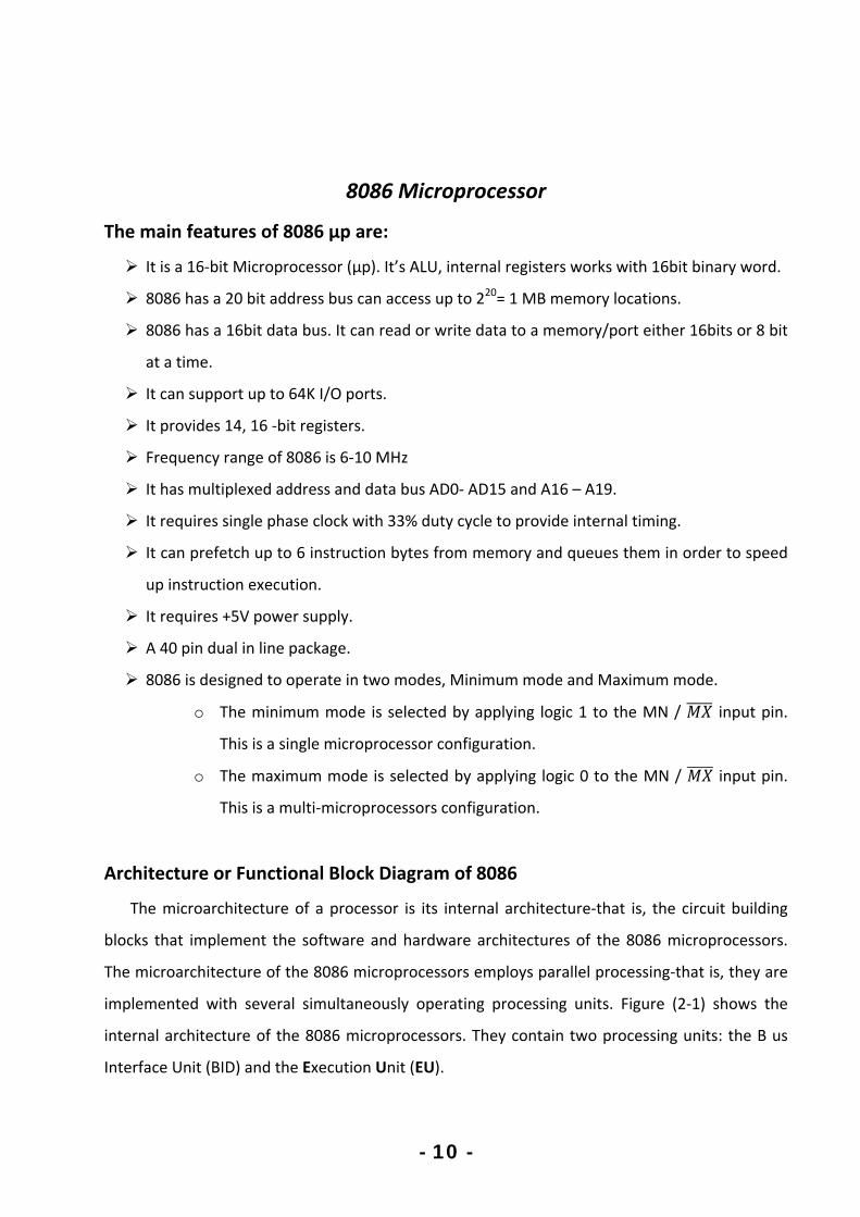
Architecture or Functional Block Diagram of 8086
The microarchitecture of a processor is its internal architecture‐that is, the circuit building
blocks that implement the software and hardware architectures of the 8086 microprocessors.
The microarchitecture of the 8086 microprocessors employs parallel processing‐that is, they are
implemented with several simultaneously operating processing units. Figure (2‐1) shows the
internal architecture of the 8086 microprocessors. They contain two processing units: the B us
Interface Unit (BID) and the Execution Unit (EU).

- 11 -
BUS INTERFACE UNIT:
It provides a full 16 bit bidirectional data bus and 20 bit address bus.
The bus interface unit connects the microprocessor to external devices. BIU performs
following operations:
Instruction fetching
Reading and writing data of data operands for memory
Inputting/outputting data for input/output peripherals.
And other functions related to instruction and data acquisition.
To implement above functions, the BIU contains the segment registers, the instruction
pointer, address generation adder, bus control logic, and an instruction queue.
The BIU uses a mechanism known as an instruction stream queue to implement pipeline
architecture.
BIU EU
Fig. (2.1): Internal architecture of the 8086 microprocessor.

EXECUT
Softwa
As a
and BIU
program
TION UNIT
The Execut
The EU con
registers, a
The EU ex
generates o
read or wr
instruction
During the
updates the
are Mode
a programm
U. The 8086
mmer. It is d
Four Gener
Four Index/
Four Segme
Two other
ion unit is r
nsists of ari
nd tempora
xtracts instr
operands if
rite by cycle
on the ope
execution
em based o
el of the 80
mer of the 8
6 micropro
divided into
ral purpose
/Pointer reg
ent register
register
Fig. (2.2): S
responsible
ithmetic log
ary‐operand
ructions fro
f necessary,
es to mem
erands.
of the inst
on the resul
086 Micro
8086 you m
cessor has
o four group
registers
gisters
rs
Software M
- 12
for decodin
gic unit (AL
d registers.
om the top
, passes the
ory or I/O
truction, th
ts of execut
oprocesso
must become
a total of
ps. They are
odel of the
-
ng and exec
LU), status a
p of the q
em to the B
and perfor
he EU tests
ting the inst
or
e familiar w
fourteen re
e:
e 8086 micro
cuting all ins
and control
ueue in th
BIU and req
rm the ope
s the status
truction.
with the var
egisters tha
oprocessor
structions.
l flags, gene
he BIU, dec
quests it to
eration spec
s and contr
rious registe
at are acces
.
eral‐purpos
codes them
perform th
cified by th
rol flags an
ers in the E
ssible to th
se
m,
he
he
nd
U
he

Gener
Accumu
and use
contain
manipu
Base re
used as
contain
indexed
Count r
used as
word, a
instruct
Data re
used as
word, a
operati
word of
Index
Source
address
conjunc
al purpos
ulator regis
ed as a 16‐b
ns the high
ulation.
egister cons
s a 16‐bit r
ns the high‐
d or register
register con
s a 16‐bit r
and CH con
tions and as
egister cons
s a 16‐bit r
and DH con
ons. In inte
f the initial
or Pointe
These regis
Index (SI) i
sing, as we
ction with t
e register
ster consists
bit register
h‐order by
sists of two
register BX.
order byte.
r indirect ad
nsists of tw
register CX
ntains the h
s a counter
sists of two
register DX.
ntains the h
eger 32‐bit
or resulting
r Register
sters can als
is a 16‐bit r
ell as a so
he DS regist
rs:
s of two 8‐b
AX. AL in th
yte. Accum
o 8‐bit regis
BL in this
. BX registe
ddressing.
wo 8‐bit reg
. When com
high‐order
in string ma
o 8‐bit regis
. When com
high‐order b
multiply an
g number.
rs
so be called
register. SI
ource data
ter to point
- 13
bit registers
his case con
mulator can
sters BL an
case conta
er usually co
gisters CL an
mbined, CL
byte. Coun
anipulation
sters DL an
mbined, DL
byte. Data r
nd divide in
d as Special
is used for
address in
t to data loc
-
s AL and AH
ntains the lo
n be used
nd BH, whic
ains the low
ontains a d
nd CH, whic
L register c
nt register
nd DH, whic
register co
register can
struction th
Purpose reg
indexed, b
n string m
cations in th
H, which can
oworder by
for I/O
ch can be c
w‐order byt
ata pointer
ch can be c
ontains the
can be use
ch can be c
ontains the
n be used a
he DX regis
gisters.
ased indexe
anipulation
he data segm
n be combin
yte of the w
operations
combined t
te of the w
r used for b
combined t
e loworder
ed in Loop,
combined t
low order
as a port nu
ster contain
ed and regi
n instructio
ment.
ned togethe
word, and A
and strin
ogether an
word, and B
based, base
ogether an
byte of th
shift/rotat
ogether an
byte of th
umber in I/O
ns high‐orde
ister indirec
ons. Used i
er
H
ng
nd
H
ed
nd
he
te
nd
he
O
er
ct
in

Destina
operati
destina
Source
Stack P
of the t
segmen
specify
Base Po
subrout
usually
Segme
There a
where
segmen
Code s
instruct
instruct
automa
ation Index
ons. DI is u
tion data a
Index regist
Pointer (SP)
top of stack
nt (specified
the offset o
ointer (BP)
tines to loca
used for ba
ent Regist
Most of th
are four diff
in 1 MB of
nt registers.
egment (CS
tions. The
tion pointe
atically upda
x (DI) is a 1
used for ind
address in s
ters are use
is a 16‐bit
k. The stac
d by the SS
of other pro
is a 16‐bit
ate variable
ased, based
ters
he registers
ferent 64 K
f processor
S) is a 16‐b
processor
er (IP) regis
ated during
16‐bit regis
dexed, base
string mani
ed to hold a
register po
k is mainta
S segment
ogram segm
t register p
es that were
indexed or
s contain d
KB segment
r memory t
bit register
uses CS se
ster. CS re
g far jump, f
- 14
ster. Used i
ed indexed
pulation ins
address.
ointing to pr
ined as a L
register).Un
ments.
pointing to
e passed on
r register in
ata/instruct
s for instru
these 4 seg
r containing
egment for
gister cann
far call and
-
in conjunct
and registe
structions.
rogram stac
LIFO with it
nlike the SP
data in sta
n the stack
direct addre
tion offsets
ctions, stac
gments are
g address o
r all access
not be cha
far return in
tion with th
er indirect a
In short, D
ck, ie it is us
s bottom a
P register,
ack segmen
by a calling
essing.
s within 64
ck, data and
e located th
of 64 KB se
ses to instr
nged direc
nstructions
he ES regis
addressing,
estination
sed to hold
at the start
the BP can
nt. It is usu
program. B
4 KB memo
d extra data
he processo
egment wit
ructions re
ctly. The CS
.
ster in strin
as well as
Index and S
the addres
of the stac
n be used t
ally used b
BP register
ory segmen
a. To specif
or uses fou
th processo
ferenced b
S register
ng
a
SI
ss
ck
to
by
is
t.
fy
ur
or
by
is

- 15 -
Stack segment (SS) is a 16‐bit register containing address of 64KB segment with program stack.
By default, the processor assumes that all data referenced by the stack pointer (SP) and base
pointer (BP) registers is located in the stack segment. SS register can be changed directly using
POP instruction.
Data segment (DS) is a 16‐bit register containing address of 64KB segment with program data.
By default, the processor assumes that all data referenced by general registers (AX, BX, CX, DX)
and index register (SI, DI) is located in the data segment. DS register can be changed directly
using POP and LDS instructions.
Extra segment (ES) used to hold the starting address of Extra segment. Extra segment is
provided for programs that need to access a second data segment. Segment registers cannot be
used in arithmetic operations.
Other registers of 8086
Instruction Pointer (IP) is a 16‐bit register. This is a crucially important register which is used to
control which instruction the CPU executes. The ip, or program counter, is used to store the
memory location of the next instruction to be executed. The CPU checks the program counter to
ascertain which instruction to carry out next. It then updates the program counter to point to
the next instruction. Thus the program counter will always point to the next instruction to be
executed.
Flag Register determines the current state of the processor. They are modified automatically by
CPU after mathematical operations, this allows to determine the type of the result, and to
determine conditions to transfer control to other parts of the program. 8086 has 9 flags and they
are divided into two categories:
1. Status Flags
Status Flags represent result of last arithmetic or logical instruction executed. Conditional
flags are as follows:
Carry Flag (CF): This flag indicates an overflow condition for unsigned integer arithmetic.
It is also used in multiple‐precision arithmetic.
Auxiliary Flag (AF): If an operation performed in ALU generates a carry/barrow from lower
nibble (i.e. D0 D3) to upper nibble (i.e. D4 – D7), the AF flag is set i.e. carry given by D3 bit to

- 16 -
D4 is AF flag. This is not a general‐purpose flag, it is used internally by the processor to
perform Binary to BCD conversion.
Parity Flag (PF): This flag is used to indicate the parity of result. If lower order 8‐bits of the
result contains even number of 1‟s, the Parity Flag is set and for odd number of 1‟s, the
Parity Flag is reset.
Zero Flag (ZF): It is set; if the result of arithmetic or logical operation is zero else it is reset.
Sign Flag (SF): In sign magnitude format the sign of number is indicated by MSB bit. If the
result of operation is negative, sign flag is set.
Overflow Flag (OF): It occurs when signed numbers are added or subtracted. An OF
indicates that the result has exceeded the capacity of machine.
2. Control Flags
Control flags are set or reset deliberately to control the operations of the execution unit.
Control flags are as follows:
1. Trap Flag (TP):
It is used for single step control.
It allows user to execute one instruction of a program at a time for debugging.
When trap flag is set, program can be run in single step mode.
2. Interrupt Flag (IF):
It is an interrupt enable/disable flag.
If it is set, the maskable interrupt of 8086 is enabled and if it is reset, the interrupt
is disabled.
It can be set by executing instruction sit and can be cleared by executing CLI
instruction.

- 17 -
3. Direction Flag (DF):
It is used in string operation.
If it is set, string bytes are accessed from higher memory address to lower memory
address.
When it is reset, the string bytes are accessed from lower memory address to
higher memory address.
MEMORY SEGMENTATION
The 8086 microprocessor operate in
the Real mode memory addressing. Real
mode operation allows the microprocessor to
address only the first 1M byte of memory
space. The first 1M byte of memory is called
either the real memory or conventional
memory system. Even though the 8086 has a
1M byte address space, not all this memory is
active at one time. Actually, the 1M bytes of
memory are partitioned into 64K byte
(65,536) segments. The 8086‐80286
microprocessors allow four memory segments. Figure 2‐3
shows these memory segments.
Think of segments as windows that can be moved over any area of memory to access
data or code. Also note that a program can have more than four segments, but can only access
four segments at a time.
Example: Let the segment registers be assigned as follow: CS = 0009H, DS = 0FFFH, SS =
10E0, and ES = 3281H. We note here that code segment and data segment are overlapped while
other segments are disjointed.
Fig. (2.3): Real Mode, Segmented Memory Model.

- 18 -
In the real mode a combinational of a segment address and offset address access a
memory location. All real mode memory address must consist of a segment address plus an
offset address. The microprocessor has a set of rules that apply to segments whenever memory
is addressed. These rules define the segment register and offset register combination (see Table
2‐1). For example, the code segment register is always used with the instruction pointer to
address the next instruction in a program. This combination is CS:IP. The code segment register
defines the start of the code segment and the instruction pointer locates the next instruction
within the code segment
TABLE (2‐1): 8086 default 16 bit segment and offset address combinations
Segment Offset Special Purpose
CS IP Instruction address
SS BP Stack address
SS SP Top of the stack
DS BX, DI,SI, an 8‐bit number, or a 16‐bit number Data address
ES DI for string instructions String destination address
This combination (CS:IP) locates the next instruction executed by the microprocessor. For
example if CS = 1400H and IP = 1200H, the microprocessor fetches its next instruction from
memory location:

- 19 -
Physical address=Segment base address*10+Offset (Effective) address
PA = SBA * 10+ EA
=1400H*10+1200H=15200H.
Q: What is segmentation? What are its advantages? How is segmentation implemented in typical microprocessors? Ans:
Segment memory addressing divides the memory into many segments. Each of these segments can be considered as a linear memory space. Each of these segment is addressed by a segment register. However since the segment register is 16 bit wide and the memory needs 20 bits for an address the 8086 appends four bits segment register to obtain the segment address. Therefore, to address the segment 10000H by , say the SS register, the SS must contain 1000H. The first advantage that memory segmentation has is that only 16 bit registers are required both to store segment base address as well as offset address. This makes the internal circuitry easier to build as it removes the requirement for 20 bits register in case the linear addressing method is used. The second advantage is relocatability.
Fig. (2.3): Generating a physical address

- 20 -
8086 Addressing Mode
Introduction
Program is a sequence of commands used to tell a microcomputer what to do.
Each command in a program is an instruction
Programs must always be coded in machine language before they can be executed by the
microprocessor.
A program written in machine language is often referred to as machine code.
Machine code is encoded using 0s and 1s
A single machine language instruction can take up one or more bytes of code
In assembly language, each instruction is described with alphanumeric symbols instead of
with 0s and 1s
Instruction can be divided into two parts : its opcode and operands
Op‐code identify the operation that is to be performed.
Each opcode is assigned a unique letter combination called a mnemonic.
Operands describe the data that are to be processed as the microprocessor carried out,
the operation specified by the opcode.
For example, the move instruction is one of the instructions in the data transfer group of
the 8086 instruction set.
Execution of this instruction transfers a byte or a word of data from a source location to a
destination location.
Addressing Mode of 8086
An addressing mode is a method of specifying an operand. The 8086 addressing modes
categorized into three types:
1. Register Addressing 2. Immediate Addressing
3. Memory Addressing
Register addressing mode
In this addressing mode, the operands may be:
reg16: 16‐bit general registers: AX, BX, CX, DX, SI, DI, SP or BP.
reg8 : 8‐bit general registers: AH, BH, CH, DH, AL, BL, CL, or DL.

- 21 -
Sreg : segment registers: CS, DS, ES, or SS. There is an exception: CS cannot be a
destination.
For register addressing modes, there is no need to compute the effective address. The operand
is in a register and to get the operand there is no memory access involved.
Example: Register Operands
MOV AX, BX ; mov reg16, reg16
ADD AX, SI ; add reg16, reg16
MOV DS, AX ; mov Sreg, reg16
Some rules in register addressing modes:
1. You may not specify CS as the destination operand.
Example: MOV CS, 02H –> wrong
2. Only one of the operands can be a segment register. You cannot move data from one segment
register to another with a single MOV instruction. To copy the value of CS to DS, you would have
to use some sequence like:
MOV DS,CS ‐> wrong
MOV AX, CS
MOV DS, AX ‐> the way we do it
3. You should never use the segment registers as data registers to hold arbitrary values. They
should only contain segment addresses.
Immediate Addressing Mode
In this addressing mode, the operand is stored as part of the instruction. The immediate
operand, which is stored along with the instruction, resides in the code segment ‐‐ not in the
data segment. This addressing mode is also faster to execute an instruction because the operand
is read with the instruction from memory. Here are some examples:
Example: Immediate Operands
MOV AL, 20 ; Copies a 20 decimal into register AL
MOV BX,55H ; Copies a 0055H into register BX
MOV SI,0 ; Copies a 0000H into register SI
MOV DX, ‘Ahmed’ ; Copies an ASCII Ahmed into register DX
MOV CL, 10101001B ; Copies a 10101001 binary into register CL
Memory Addressing Modes
To reference an operand in memory, the 8086 must calculate the physical address (PA) of
the operand and then initiate a read or write operation of this storage location. The 8086 MPU is
provided with a group of addressing modes known as the memory operand addressing modes

- 22 -
for this purpose. Physical address can computed from a segment base address (SBA) and an
effective address (EA). SBA identifies the starting location of the segment in memory, and EA
represents the offset of the operand from the beginning of this segment of memory. PA=SBA (segment): EA (offset)
PA=segment base: base + index + Displacement
There are different forms of memory addressing modes 1. Direct Addressing
2. Register indirect addressing
3. Based addressing
4. Indexed addressing
5. Based indexed addressing
6. Based indexed with displacement
1. Direct Addressing Mode Direct addressing mode is similar to immediate addressing in that information is encoded
directly into the instruction. However, in this case, the instruction opcode is followed by an effective address, instead of the data. As shown below:
For example the instruction
Example: Immediate Operands
MOV AL, DS:[2000H] ; move the contents of the memory location with offset 2000
or MOV AL, [2000H] into register AL
MOV AL,DS:[8088H] ; move the contents of the memory location with offset 8088
or MOV AL,[8088H] into register AL
MOV DS:[1234H],DL ; stores the value in the DL register to memory location with
or MOV [1234H],DL offset 1234H

- 23 -
By default, all displacement‐only values provide offsets into the data segment. If you
want to provide an offset into a different segment, you must use a segment override prefix
before your address. For example, to access location 1234H in the extra segment (ES) you would
use an instruction of the form MOV AX,ES:[1234H]. Likewise, to access this location in the code
segment you would use the instruction MOV AX, CS:[1234H].
2. Register Indirect Addressing Mode
This mode is similar to the direct address except that the effective address held in any of
the following register: BP, BX, SI, and DI. As shown below:
MOV AL, [BX]
MOV AL, [BP]
MOV AL, [SI]
MOV AL, [DI]
The [BX], [SI], and [DI] modes use the DS segment by default. The [BP] addressing mode uses the
stack segment (SS) by default. You can use the segment override prefix symbols if you wish to
access data in different segments. The following instructions demonstrate the use of these
overrides:
MOV AL, CS:[BX]
MOV AL, DS:[BP]
MOV AL, SS:[SI]
MOV AL, ES:[DI]
For example:
MOV SI, 1234H
MOV AL, [SI]
If SI contains 1234H and DS contains 0200H the result produced by executing the instruction is
that the contents of the memory location at address:
PA = 02000H + 1234H
= 03234 are moved to the AX register.
3. Based Addressing Mode
In the based addressing mode, the effective address of the operand is obtained by adding
a direct or indirect displacement to the contents of
either base register BX or base pointer register BP.
The physical addresses calculate as shown:

- 24 -
For example if BX=1000, DS=0200, and AL=EDH, for the following instruction:
MOV [BX] + 1234H, AL
EA=BX+1234H = 1000H+1234H = 2234H
PH=DS*10+EA =0200H*10+2234H = 4234H
So it writes the contents of source operand AL (EDH) into the memory location 04234H. If BP is
used instead of BX, the calculation of the physical address is performed using the contents of the
stack segment (SS) register instead of DS. This permits access to data in the stack segment of
memory.
4. Indexed Addressing Modes
In the Indexed addressing mode, the effective address of the operand is obtained by
adding a direct or indirect displacement to the contents of either SI or DI register. The physical
addresses calculate as shown below:
The indexed addressing modes use the
following syntax:
MOV AL, [SI]
MOV AL, [DI]
MOV AL, [SI+DISP]
MOV AL, [DI+DISP]
5. Based Indexed Addressing Modes
Combining the based addressing mode and the indexed addressing mode results in a
new, more powerful mode known as based‐indexed addressing mode. This addressing mode can
be used to access complex data structures such as two‐dimensional arrays. As shown below this
mode can be used to access elements in an m X n array of data. Notice that the displacement,
which is a fixed value, locates the array in memory. The base register specifies the m coordinate

of the a
base an
Suppos
would l
Likewis
will load
The add
BP as an
6. Ba
with th
these a
MOV
MOV
MOV
MOV
You ma
above t
address
array, and t
nd index reg
MOV AL,
MOV AL,
MOV AL,
MOV AL,
e that BX co
oad AL from
e, if BP con
d the 16 bit
dressing mo
n operand u
ased Index
These addr
e addition
ddressing m
AL, DISP[BX
AL, DISP[BX
AL, [BP+SI+
AL, [BP][DI
ay substitute
to produce t
sing mode.
he index re
gisters perm
[BX+SI]
[BX+DI]
[BP+SI]
[BP+DI]
ontains 100
MOV
m location D
tains 1598h
MOV AX
ts in AX from
odes that do
use the stac
xed Plus D
ressing mod
of an eight
modes
X][SI]
X+DI]
+DISP]
I][DISP]
e DI in the f
the [BX+DI+
egister ident
mits access t
00H and si c
AL,[BX][SI]
DS:1880h.
h and DI con
X,[BP+DI]
m locations
o not involv
ck segment
Displacem
des are a sli
t bit or sixt
figure
+disp]
- 25
tifies the n
to any elem
contains 880
ntains 1004
SS:259C an
ve BP use th
by default.
ment Addre
ight modific
teen bit co
-
coordinate
ment in the a
0H. Then th
4,
nd SS:259D.
he data segm
essing Mo
cation of th
nstant. The
. Simply cha
array.
e instructio
ment by def
ode
he base/ind
e following
anging the v
on
fault. Those
exed addre
are some
values in th
e that have
essing mode
examples o
he
es
of

- 26 -
Q: Compute the physical address for the specified operand in each of the following instructions. The register contents and variable are as follows: (CS)=0A00H, (DS)=0B00H, (SS)=0D00H, (SI)=0FF0H, (DI)=00B0H, (BP)=00EAH and (IP)=0000H, LIST=00F0H, AX=4020H, BX=2500H.
1) Destination operand of the instruction MOV LIST [BP+DI] , AX
2) Source operand of the instruction MOV CL , [BX+200H]
3) Destination operand of the instruction MOV [DI+6400H] , DX
4) Source operand of the instruction MOV AL, [BP+SI‐400H]
5) Destination operand of the instruction MOV [DI+SP] , AX
6) Source operand of the instruction MOV CL , [SP+200H]
7) Destination operand of the instruction MOV [BX+DI+6400H] , CX
8) Source operand of the instruction MOV AL , [BP‐ 0200H]
9) Destination operand of the instruction MOV [SI] , AX
10) Destination operand of the instruction MOV [BX][DI]+0400H,AL
11) Source operand of the instruction MOV AX, [BP+200H]
12) Source operand of the instruction MOV AL, [SI‐0100H]
13) Destination operand of the instruction MOV DI,[SI]
14) Destination operand of the instruction MOV [DI]+CF00H,AH
15) Source operand of the instruction MOV CL, LIST[BX+200H]

- 27 -
8086 Instruction Set The instructions of 8086 are classified into SIX groups. They are:
1. DATA TRANSFER INSTRUCTIONS 2. ARITHMETIC INSTRUCTIONS 3. BIT MANIPULATION INSTRUCTIONS 4. STRING INSTRUCTIONS 5. PROGRAM EXECUTION TRANSFER INSTRUCTIONS 6. PROCESS CONTROL INSTRUCTIONS
1. DATA TRANSFER INSTRUCTIONS The DATA TRANSFER INSTRUCTIONS are those, which transfers the DATA from any one
source to any one destination. The data’s may be of any type. They are again classified into four groups. They are:
General – Purpose Byte Or Word Transfer Instructions
Special Address Transfer Instruction
Simple Input And Output Port Transfer Instruction
Flag Transfer Instructions
MOV XCHG XLAT PUSH POP
LEA LDS LES
IN OUT
LAHF SAHF PUSHF POPF
MOV Instruction
The MOV instruction copies a word or a byte of data from a specified source to a specified destination. Data can be moved between general purpose‐registers, between a general purpose‐register and a segment register, between a general purpose‐register or segment register and memory, or between a memory location and the accumulator. Note that memory‐to‐memory transfers are note allowed.
Mnemonic Meaning Format Operation Flags Effected
MOV Move MOV D,S (S) (D) none
Example:
MOV CX, 037AH ; Move 037AH into the CX; 037A CX
MOV AX, BX ; Copy the contents of register BX to AX ; BX AX
MOV DL,[BX] ; Copy byte from memory at BX to DL ; DS*10+BX DL
- 28 -
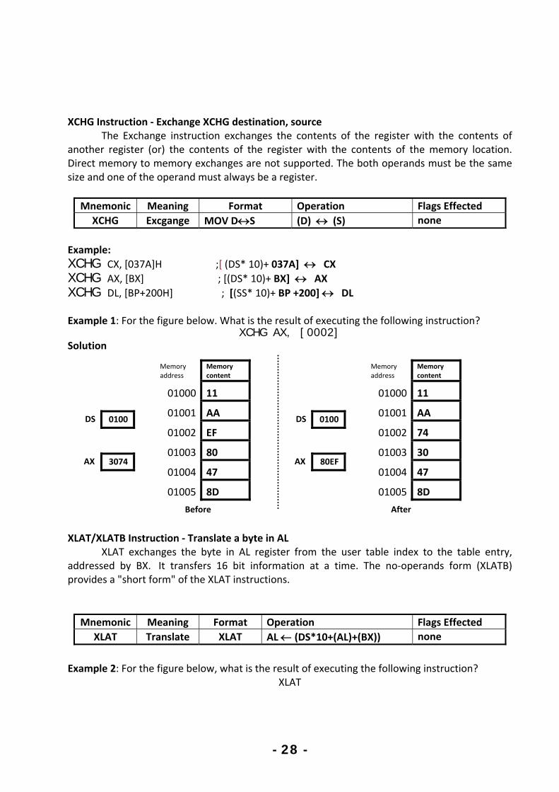
XCHG Instruction ‐ Exchange XCHG destination, source The Exchange instruction exchanges the contents of the register with the contents of
another register (or) the contents of the register with the contents of the memory location. Direct memory to memory exchanges are not supported. The both operands must be the same size and one of the operand must always be a register.
Mnemonic Meaning Format Operation Flags Effected
XCHG Excgange MOV DS (D) (S) none
Example:
XCHG CX, [037A]H ;[ (DS* 10)+ 037A] CX
XCHG AX, [BX] ; [(DS* 10)+ BX] AX
XCHG DL, [BP+200H] ; [(SS* 10)+ BP +200] DL Example 1: For the figure below. What is the result of executing the following instruction?
XCHG AX, [0002] Solution
XLAT/XLATB Instruction ‐ Translate a byte in AL
XLAT exchanges the byte in AL register from the user table index to the table entry, addressed by BX. It transfers 16 bit information at a time. The no‐operands form (XLATB) provides a "short form" of the XLAT instructions.
Mnemonic Meaning Format Operation Flags Effected
XLAT Translate XLAT AL (DS*10+(AL)+(BX)) none
Example 2: For the figure below, what is the result of executing the following instruction?
XLAT
Memory address
Memory content
01000 11
01001 AA
01002 EF
01003 80
01004 47
01005 8D
0100
3074
DS
AX
Memory address
Memory content
01000 11
01001 AA
01002 74
01003 30
01004 47
01005 8D
0100
80EF
DS
AX
Before After

- 29 -
Solution:
The stack The stack is implemented in the memory and it is used for temporary storage of
information such as data and addresses. The stack is 64Kbytes long and is organized from a software point of view as 32Kwords. • SS register points to the lowest address word in the stack • SP and BP points to the address within stack • Data transferred to and from the stack are word‐wide, not byte‐wide. • The first address in the Stack segment (SS : 0000) is called End of Stack. • The last address in the Stack segment (SS : FFFE) is called Bottom of Stack. • The address (SS:SP) is called Top of Stack.
Memory address
Memory content
01040 11
01041 AA
01042 EF
01043 80
01044 47
01045 8D
0100
xx03
DS
AX
Memory address
Memory content
01040 11
01041 AA
01042 74
01043 80
01044 47
01045 8D
0100
Xx80
DS
AX
Before After
BX 0040 0040 BX

- 30 -
PUSH and POP Instructions The PUSH and POP instructions are important instructions that store and retrieve data
from the LIFO (Last In First Out) stack memory. The general forms of PUSH and POP instructions are as shown below:
Mnemonic Meaning Format Operation Flags Effected
PUSH Push word onto the stack PUSH S (SP) (SP‐2)
((SP)) (S) None
POP Pop word off stack POP D D ((SP)) (SP) = (SP+2)
None
• POP instruction is used to read word from the stack. • PUSH instruction is used to write word to the stack. • When a word is to be pushed onto the top of the stack:
o The value of SP is first automatically decremented by two o and then the contents of the register written into the stack.
• When a word is to be popped from the top of the stack the o the contents are first moved out the stack to the specific register o then the value of SP is incremented by two.
Example 3: let AX=1234H, SS=0105H and SP=0006H. Figure below shows the state of stack prior and after the execution of next program instructions: PUSH AX POP BX POP AX
(a) Initial State (b) After execution of PUSH AX
Memory address
Memory content
01058 90
01057 DD
01056 DF
01055 1F
01054 55
01053 52
01052 C0
01051 00
01050 02
1234 AX
SP
SS
0006
0105
5D00 BX
Memory address
Memory content
01058 90
01057 DD
01056 DF
01055 12
01054 34
01053 52
01052 C0
01051 00
01050 02
1234 AX
SP
SS
0004
0105
5D00 BX

- 31 -
LEA, LDS, and LES (Load Effective Address) Instructions
These instructions load a segment and general purpose registers with an address directly from memory. The general forms of these instructions are as shown below:
Mnemonic Meaning Format Operation Flags Effected
LEA Load register with Effective Address
LEA reg16, EA EA (reg16) none
LDS Load register and Ds with words from memory
LDS reg16, EA [PA] (reg16)
[PA+2] (DS) none
LES Load register and ES with words from memory
LES reg16, EA [PA] (reg16)
[PA+2] (ES) None
Example4: LEA BX, PRICE ;Load BX with offset of PRICE in DS LEA BP, SS:STAK ;Load BP with offset of STACK in SS LEA CX, [BX][DI] ;Load CX with EA=BX + DI LDS BX, [4326] ; copy the contents of the memory at displacement 4326H in DS to BL, contents of the 4327H to BH. Copy contents of 4328H and 4329H in DS to DS register. Example 5: Assuming that (BX)=100H, DI=200H, DS=1200H, SI= F002H, AX= 0105H, and the following memory content. what is the result of executing the following instructions?
a. LEA SI , [ DI + BX +2H] b. MOV SI , [DI+BX+2H] c. LDS CX , [300] d. LES BX , [DI+AX]
Memory address
Memory content
12300 11
12301 AA
12302 EF
12303 80
12304 47
12305 8D
12306 5A
12307 92
12308 C5
(c) After execution of POP BX (d) After execution of POP AX
Memory address
Memory content
01058 90
01057 DD
01056 DF
01055 12
01054 34
01053 52
01052 C0
01051 00
01050 02
1234 AX
SP
SS
0006
0105
1234 BX
Memory address
Memory content
01058 90
01057 DD
01056 DF
01055 12
01054 34
01053 52
01052 C0
01051 00
01050 02
DDDF AX
SP
SS
0008
0105
1234 BX

- 32 -
Solution: a. LEA SI , [ DI + BX +2H SI = (DI) + (BX) + 2H= 0200H+0100H+0002H= 0302H b. MOV SI , [DI+BX+2H] EA=(DI+BX+2H)= 0302H PA=DS*10+EA=1200*10+0302=12302 SI = 80EFH c. LDS CX , [300] PA = DS*10+EA= 1200H*10+300H = 12300H CX= AA11H and DS=80EFH d. LES BX , [DI+AX] EA = (DI+AX)= 0200H+0105H =0305H PA= DS*10+EA = 1200H*10+0305H = 12305H BX = 5A8DH and ES = C592H IN and OUT Instruction
There are two different forms of IN and OUT instructions: the direct I/O instructions and variable I/O instructions. Either of these two types of instructions can be used to transfer a byte or a word of data. All data transfers take place between an I/O device and the MPU’s accumulator register. The general form of this instruction is as shown below:
Mnemonic Meaning Format Operation Flags Effected
IN Input direct Input variable
IN Acc, Port IN Acc, DX
(Acc) (Port)
(Acc) (DX) none
OUT Output direct Output variable
OUT Port, Acc OUT DX , Acc
(Port) (Acc)
(DX) (Acc) none
Example: IN AL,0C8H ;Input a byte from port 0C8H to AL IN AX, 34H ;Input a word from port 34H to AX OUT 3BH, AL ;Copy the contents of the AL to port 3Bh OUT 2CH,AX ;Copy the contents of the AX to port 2Ch For a variable port IN instruction, the port address is loaded in DX register before IN instruction. DX is 16 bit. Port address range from 0000H – FFFFH. Example: (a) MOV DX, 0FF78H ;Initialize DX point to port IN AL, DX ;Input a byte from a 8 bit port 0FF78H to AL IN AX, DX ;Input a word from 16 bit port to 0FF78H to AX. Example: (b)

- 33 -
MOV DX, 0FFF8H ;Load desired port address in DX OUT DX, AL ; Copy the contents of AL to FFF8h OUT DX, AX ;Copy content of AX to port FFF8H LAHF Instruction ‐ Load Register AH From Flags
LAHF instruction copies the value of SF, ZF, AF, PF, and CF, into bits of 7, 6, 4, 2, 0 respectively of AH register. This LAHF instruction was provided to make conversion of assembly language programs written for 8080 and 8085 to 8086 easier. SAHF instruction ‐ Store AH Register into FLAGS
SAHF instruction transfers the bits 0‐7 of AH of SF, ZF, AF, PF, and CF, into the Flag register. PUSHF Instruction ‐ Push flag register on the stack
This instruction decrements the SP by 2 and copies the word in flag register to the memory location pointed to by SP. POPF Instruction ‐ Pop word from top of stack to flag ‐ register.
This instruction copies a word from the two memory location at the top of the stack to flag register and increments the stack pointer by 2.

- 34 -
Signed and Unsigned Numbers
An 8 bit number system can be used to create 256 combinations (from 0 to 255), and the first 128 combinations (0 to 127) represent positive numbers and next 128 combinations (128 to 255) represent negative numbers.
Unsigned Number
Binary Hexa. Signed Number
0 0000 0000 00 0
1 0000 0001 01 +1
2 0000 0010 02 +2
127 0111 1111 7F +127
128 1000 0000 80 -128
129 1000 0001 81 -127
254 1111 1110 FE -2
255 1111 1111 FF -1
In Decimal in order to get ‐ 2, we subtract 2 from the number of combinations (256),
which gives, 256 ‐ 2 = 254. In Binary all the Signed Numbers have a '1' in the Most Significant Bit (MSB) position
which represents a negative number and a '0' in the Most Significant Bit (MSB) position which represents a positive number. Also, in Binary, the 2's Complement of a number is the negative equivalent of the positive number.
Equation Binary Hex Signed
2 = 0000 0010 02 +2
1's Complement = 1111 1101 FD
Add '1' +0000 0001 +01
2's Complement = 1111 1110 FE ‐2
So, as above, +2 = 0000 0010 and the 2's Complement is 1111 1110 which represents ‐ 2.

- 35 -
A 16 bit number system can be used to create 65536 combinations (from 0 to 65535), and the first 32768 combinations (0 to 32767) represent positive numbers and next 32768 combinations (32768 to 65536) represent negative numbers.
In a 16 bit number system the Signed Numbers have a '1' in the Most Significant Bit (MSB) position 1xxx xxxx xxxx xxxx which represents a negative number. A '0' in the Most Significant Bit (MSB) position 0xxx xxxx xxxx xxxx which represents a positive number.
2. ARITHMETIC INSTRUCTIONS These instructions are those which are useful to perform Arithmetic calculations, such as
addition, subtraction, multiplication and division. They are again classified into four groups. They are:
Addition Instructions
Subtraction Instructions
Multiplication Instructions
Division Instructions
ADD ADC INC AAA DAA
SUB SBB DEC NEG CMP AAS DAS
MUL IMUL AAM
DIV IDIV AAD CBW CWD
The state that results from the execution of an arithmetic instruction is recorded in the
flags register. The flags that are affected by the arithmetic instructions are C, A, S, Z, P, O.
2.1 Addition Instructions: The general forms of these instructions are shown below
Mnemonic Meaning Format Operation Flags Effected
ADD Addition ADD D, S (S)+(D) (D)
carry (CF) O, S, Z, A, P, C
ADC Add with carry ADC D, S (S)+(D) +(CF) (D)
carry (CF) O, S, Z, A, P, C
INC Increment by 1 INC D (D)+1 D O, S, Z, A, P
DAA Decimal adjust for addition DAA S, Z, A, P, C
AAA ASCII adjust for addition AAA A, C
EXAMPLE: ADD AL,74H ;Add immediate number 74H to content of AL ADC CL,BL ;Add contents of BL plus carry status to contents of CL Results in CL

- 36 -
ADD DX, [SI] ;Add word from memory at offset [SI] in DS to contents of DX Addition of Un Signed numbers: ADD CL, BL Assume that CL = 01110011 =115 decimal ; BL = 01001111 = 79 decimal Result in CL = 11000010 = 194 decimal Addition of Signed numbers ADD CL, BL Assume that CL = 01110011 = + 115 decimal ; BL = 01001111 = +79 decimal Result in CL = 11000010 = ‐ 62 decimal ; Incorrect because result is too large to fit in 7 bits. INC Instruction ‐ Increment ‐ INC destination
INC instruction adds one to the operand and sets the flag according to the result. INC instruction is treated as an unsigned binary number. Example: Assume AX = 7FFFh INC AX ;After this instruction AX = 8000h DAA Instruction ‐ Decimal Adjust after Addition The contents after addition are changed from a binary value to two 4‐bit binary coded
decimal (BCD) digits. S, Z, AC, P, CY flags are altered to reflect the results of the operation.
DAA instruction used to perform an adjust operation similar to that performed by AAA but for the addition of packed BCD numbers instead of ASCII numbers.
Since DAA can adjust only data that are in AL, the destination register for ADD instructions that process BCD numbers should be AL.
DAA must be invoked after the addition of two packed BCD numbers. Example: Assume that AL contains 29H (the BCD code for decimal number 29), BL contain 13H (the BCD code for decimal number 13), and AH has been cleared. What is the result of executing the following instruction sequence?
ADD AL, BL DAA

- 37 -
AAA Instruction ‐ ASCII Adjust after Addition AAA will adjust the result of the two ASCII characters that were in the range from 30h
(“0”) to 39h(“9”).This is because the lower 4 bits of those character fall in the range of 0‐9.The result of addition is not a ASCII character but it is a BCD digit.
AAA instruction specifically used to adjust the result after the operation of addition two binary numbers which represented in ASCII.
AAA instruction should be executed immediately after the ADD instruction that adds ASCII data.
Since AAA can adjust only data that are in AL, the destination register for ADD instructions that process ASCII numbers should be AL.
Example: what is the result of executing the following instruction sequence?
ADD AL , BL AAA
Assume that AL contains 32H (the ASCII code for number 2), BL contain 34H (the ASCII code for number 4) , and AH has been cleared. Solution:
2.2 Subtraction Instructions: Subtraction subgroup of instruction set is similar to the addition subgroup.
For subtraction the carry flag CF acts as borrow flag
If borrow occur after subtraction then CF = 1.
If NO borrow occur after subtraction then CF = 0.
Subtraction subgroup content instruction shown in table below
Mnemonic Meaning Format Operation Flags Effected
SUB Subtraction SUB D,S (S)‐(D) (D)
borrow (CF) O, S, Z, A, P, C
SBB Subtract with borrow SBB D,S (S)‐(D) ‐(CF) (D)
borrow (CF) O, S, Z, A, P, C
DEC Decrement by 1 DEC D (D)‐1 D O, S, Z, A, P
NEG Negative NEG 0 – (D) (D)
1 (CF) O, S, Z, A, P, C
CMP Compare CMP D,S (S) ‐ (D) O, S, Z, A, P, C
DAS Decimal adjust for Subtraction DAS S, Z, A, P, C
AAS ASCII adjust for Subtraction AAS A, C

- 38 -
Example: SUB CX, BX ; BX– CX; Result in CX SBB CH, AL ; AL – CH – CF ; Result in CH SBB 3427H , AX ; Subtract immediate number 3427H from AX Subtracting unsigned number Assume that CL = 10011100 = 156 decimal ; BH = 00110111 = 55 decimal SUB BH, CL CL = 01100101 = 101 decimal ; CF, AF, SF, ZF = 0, OF, PF = 1 Subtracting signed number Assume that CL = 00101110 = + 46 decimal ; BH = 01001010= + 74 decimal SUB BH, CL CL = 11100100 = ‐ 28 decimal ; CF = 1, AF, ZF =0,SF = 1 result negative DEC Instruction ‐ Decrement destination register or memory DEC destination.
DEC instruction subtracts one from the operand and sets the flag according to the result. DEC instruction is treated as an unsigned binary number. Example: MOV AX, 8000H ; AX =8000h DEC AX ; After this instruction AX = 7999h DEC BL ; Subtract 1 from the contents of BL register NEG Instruction ‐ From 2’s complement – NEG destination
NEG performs the two’s complement subtraction of the operand from zero and sets the flags according to the result. MOV AX , 2CBh NEG AX ;after executing NEG result AX =FD35h. CMP Instruction ‐ Compare byte or word ‐CMP destination, source.
The CMP instruction compares the destination and source i.e., it subtracts thesource from destination. The result is not stored anywhere. It neglects the results, but sets the flags accordingly. This instruction is usually used before a conditional jump instruction. Example: MOV AL, 5 MOV BL, 5 CMP AL, BL ; AL = 5, ZF = 1 (so equal!) RET DAS Instruction ‐ Decimal Adjust after Subtraction
This instruction corrects the result (in AL) of subtraction of two packed BCD values. The flags which modify are AF, CF, PF, SF, ZF if low nibble of AL > 9 or AF = 1 then: ‐ AL = AL – 6

- 39 -
‐ AF = 1 if AL > 9Fh or CF = 1 then: ‐ AL = AL ‐ 60h ‐ CF = 1 Example: MOV AL, 0FFh ; AL = 0FFh (‐1) DAS ; AL = 99h, CF = 1 RET AAS Instruction ‐ ASCII Adjust for Subtraction
AAS converts the result of the subtraction of two valid unpacked BCD digits to a single valid BCD number and takes the AL register as an implicit operand. The two operands of the subtraction must have its lower 4 bit contain number in the range from 0 to 9 .The AAS instruction then adjust AL so that it contain a correct BCD digit. MOV AX, 0901H ; BCD 91 SUB AL, 9 ; Minus 9 AAS ; Give AX =0802 h (BCD 82) Example:( a ) ;AL =0011 1001 =ASCII 9 ;BL=0011 0101 =ASCII 5 SUB AL, BL ;(9 ‐ 5) Result : ;AL = 00000100 = 04(BCD), CF = 0 AAS ;Result : AL=00000100 =BCD 04 , CF = 0 NO Borrow required Example:( b ) ;AL = 0011 0101 =ASCII 5 ;BL = 0011 1001 = ASCII 9 SUB AL, BL ;( 5 ‐ 9 ) Result : AL = 1111 1100 = – 4 in 2’s complement CF = 1 AAS ;Results :AL = 0000 0100 =BCD 04, CF = 1 borrow needed
2.3 Multiplication and Division Instructions The 8086 has instructions for multiplication and division of binary, BCD numbers, and
signed or unsigned integers. Multiplication and division are performed on bytes or on words. Fig below shows the form of these instructions.
Mnemonic Meaning Format Operation
MUL Multiply (Unsigned) MUL S (AL)*(S8) (AX) ; (AX)*(S16) (DX)(AX)
DIV Division (Unsigned) DIV S Q((AX)/(S8)) (AL) ; R((AX)/(S8)) (AH)
Q((DX,AX)/(S16)) (AX) ;
R((DX,AX)/(S16)) (DX)
IMUL Integer Multiply (Signed) IMUL S (AL)*(S8) (AX) ; (AX)*(S16) (DX)(AX)
IDIV Integer Divide (Signed) IDIV S Q((AX)/(S8)) (AL) ; R((AX)/(S8)) (AH)
Q((DX,AX)/(S16)) (AX) ;
R((DX,AX)/(S16)) (DX)
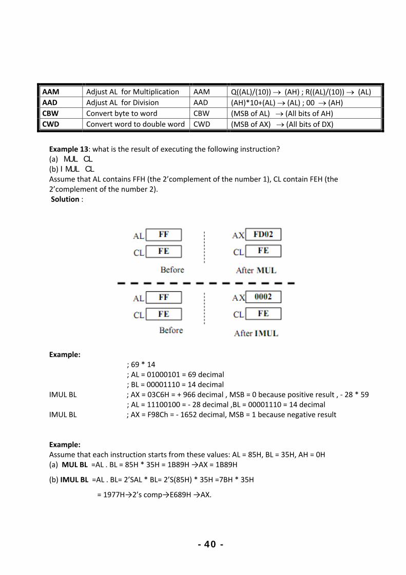
- 40 -
AAM Adjust AL for Multiplication AAM Q((AL)/(10)) (AH) ; R((AL)/(10)) (AL)
AAD Adjust AL for Division AAD (AH)*10+(AL) (AL) ; 00 (AH)
CBW Convert byte to word CBW (MSB of AL) (All bits of AH)
CWD Convert word to double word CWD (MSB of AX) (All bits of DX)
Example 13: what is the result of executing the following instruction? (a) MUL CL (b) IMUL CL Assume that AL contains FFH (the 2’complement of the number 1), CL contain FEH (the 2’complement of the number 2). Solution :
Example: ; 69 * 14 ; AL = 01000101 = 69 decimal ; BL = 00001110 = 14 decimal IMUL BL ; AX = 03C6H = + 966 decimal , MSB = 0 because positive result , ‐ 28 * 59 ; AL = 11100100 = ‐ 28 decimal ,BL = 00001110 = 14 decimal IMUL BL ; AX = F98Ch = ‐ 1652 decimal, MSB = 1 because negative result Example: Assume that each instruction starts from these values: AL = 85H, BL = 35H, AH = 0H (a) MUL BL =AL . BL = 85H * 35H = 1B89H →AX = 1B89H
(b) IMUL BL =AL . BL= 2’SAL * BL= 2’S(85H) * 35H =7BH * 35H
= 1977H→2’s comp→E689H →AX.

- 41 -
(c) DIV BL = H35
H0085
BL
AX
(d). IDIV BL = H35
H0085
BL
AX
Example: Assume that each instruction starts from these values: AL = F3H, BL = 91H, AH = 00H
(a) MUL BL = AL . BL = F3H * 91H = 89A3H →AX = 89A3H
(b) IMUL BL = AL . BL= 2’SAL * 2’SBL= 2’S(F3H) *2’S(91H) =0DH * 6FH = 05A3H →AX.
(c) DIV BL = 91H
H3F00
BL
AX 1 quotient and 62H remainder:
(d) IDIV BL = FH6
H3F00
2S(91H)
H3F00
BL
AX 2 quotient and 15H remainder:
But Negative Negative
Positive , So
Example: Assume that each instruction starts from these values: AX= F000H, BX= 9015H, DX= 0000H
(a) MUL BX = AX . BX = F000H * 9015H =
(b) IMUL BX =2’S(F000H) *2’S(9015H) = 1000 * 6FEB =
AH (remainder) AL (quotient) 1B 02
AH (remainder) AL (quotient) 1B 02
AH (remainder) AL (quotient) 62 01
AH (remainder) AL (quotient) 15 02
AH (remainder) AL (quotient) 15 2’S (02)
AH (remainder) AL (quotient) 15 FE
DX AX
8713 B000
DX AX
06FE B000

- 42 -
(c) DIV BL = DH6B015H
H000F
BL
AX more than FFH Divide Error
(d) IDIV BL = H3CH15
H1000
15H
)H000F(S'2
BL
AX more than 7FH Divide Error
Example: Assume that each instruction starts from these values: AX = 1250H, BL = 90H
(a) DIV BL = 90H
H1250
BL
AX
(b) IDIV BL = 70H
H1250
(90H)2'
H1250
negative'2
positive
negative
positive
90H
H1250
BL
AX
But Negative Negative
Positive , So
AAM Instruction ‐ ASCII adjust after Multiplication
AAM Instruction ‐ AAM converts the result of the multiplication of two valid unpacked BCD digits into a valid 2‐digit unpacked BCD number and takes AX as an implicit operand. To give a valid result the digits that have been multiplied must be in the range of 0 – 9 and the result should have been placed in the AX register. Because both operands of multiply are required to be 9 or less, the result must be less than 81 and thus is completely contained in AL. AAM unpacks the result by dividing AX by 10, placing the quotient (MSD) in AH and the remainder (LSD) in AL. Example: MOV AL, 5 MOV BL, 7 MUL BL ;Multiply AL by BL , result in AX AAM ;After AAM, AX =0305h
AH (remainder) AL (quotient) 50H 20H
AH (remainder) AL (quotient) 60H 29H
AH (remainder) AL (quotient)
60H 2’(29H) AH (remainder) AL (quotient)
60H D7H

- 43 -
AAD Instruction ‐ ASCII adjust before Division ADD converts unpacked BCD digits in the AH and AL register into a single binary number
in the AX register in preparation for a division operation. Before executing AAD, place the Most significant BCD digit in the AH register and Last significant in the AL register. When AAD is executed, the two BCD digits are combined into a single binary number by setting AL=(AH*10)+AL and clearing AH to 0. Example: MOV AX,0205h ;The unpacked BCD number 25 AAD ;After AAD , AH=0 and AL=19h (25). After the division AL will then contain the unpacked BCD quotient and AH will contain the unpacked BCD remainder. Example: ;AX=0607 unpacked BCD for 67 decimal CH=09H. AAD ;Adjust to binary before division AX=0043 = 43H =67 decimal. DIV CH ;Divide AX by unpacked BCD in CH, AL = quotient = 07 unpacked BCD, AH = remainder = 04 unpacked BCD CBW Instruction ‐ Convert signed Byte to signed word
CBW converts the signed value in the AL register into an equivalent 16 bit signed value in the AX register by duplicating the sign bit to the left. This instruction copies the sign of a byte in AL to all the bits in AH. AH is then said to be the sign extension of AL. Example: ; AX = 00000000 10011011 = ‐ 155 decimal CBW ; Convert signed byte in AL to signed word in AX. ; Result in AX = 11111111 10011011 and = ‐ 155 decimal CWD Instruction ‐ Convert Signed Word to ‐ Signed Double word
CWD converts the 16 bit signed value in the AX register into an equivalent 32 bit signed value in DX: AX register pair by duplicating the sign bit to the left. The CWD instruction sets all the bits in the DX register to the same sign bit of the AX register. The effect is to create a 32‐ bit signed result that has same integer value as the original 16 bit operand. Example: Assume AX contains C435h. If the CWD instruction is executed, DX will contain FFFFh since bit 15 (MSB) of AX was 1. Both the original value of AX (C435h) and resulting value of DX : AX (FFFFC435h) represents the same signed number. Example: ;DX = 00000000 00000000 and AX = 11110000 11000111 = ‐ 3897 decimal CWD ;Convert signed word in AX to signed double word in DX:AX ;Result DX = 11111111 11111111 and AX = 11110000 11000111 = ‐3897 decimal.

- 44 -
3. BIT MANIPULATION INSTRUCTIONS These instructions are used to perform Bit wise operations.
LOGICAL INSTRUCTIONS SHIFT INSTRUCTIONS ROTATE INSTRUCTIONS
NOT AND OR XOR TEST
SHL / SAL SHR SAR
ROL ROR RCL RCR
3.1 Logical Instructions The 8086 processor has instructions to perform bit by bit logic operation on the specified
source and destination operands. Uses any addressing mode except memory‐to‐memory and segment registers These instructions perform their respective logic operations. Figure below shows the format and the operand for these instructions.
Mnemonic Meaning Format Operation Flags Effected
NOT Logical NOT NOT D (D ) (D) None
AND Logical AND AND D,S (S) . D) (D) O, S, Z, P, C
OR Logical Inclusive OR OR D,S (S) + D) (D) O, S, Z, P, C
XOR Logical Exclusive OR XOR D,S (S) D) (D) O, S, Z, P, C
Logical AND: used to clear certain bits in the operand(masking) Example: Clear the high nibble of BL register
AND BL, 0FH ; (xxxxxxxx AND 0000 1111 = 0000 xxxx) Example: Clear bit 5 of DH register
AND DH, DFH ; (xxxxxxxx AND 1101 1111 = xx0xxxxx) Logical OR: Used to set certain bits Example: Set the lower three bits of BL register
OR BL, 07H ; (xxxxxxxx OR 0000 0111 = xxxx x111) Example: Set bit 7 of AX register
ORAH, 80H ; (xxxxxxxx OR 1000 0000 = 1xxxxxxx)
Logical XOR Used to invert certain bits (toggling bits) Used to clear a register by XORed it with itself
Example: Invert bit 2 of DL register XOR BL, 04H ; (xxxxxxxx OR 0000 0100 = xxxx x x xx)
Example: Clear DX register XOR DX, DX (DX will be 0000H)

- 45 -
3.2 Shift instructions Shift instructions can perform two basic types of shift operations; the logical shift and the
arithmetic shift. Also, each of these operations can be performed to the right or to the left. Shift instructions are used to
Align data Isolate bit of a byte of word so that it can be tested Perform simple multiply and divide computations
The source can specified in two ways Value of 1 : Shift by One bit Value of CL register : Shift by the value of CL register
Note that the amount of shift specified in the source operand can be defined explicitly if it is one bit or should be stored in CL if more than 1. SHL, SHR, SAL, and, SAR instructions:
The operation of these instructions is described in figure below.
Mnem. Meaning Format Operation Flags Effected
SAL/SHL Shift arithmetic left /shift logical left
SAL D, Count SHL D, Count
Shift the (D) left by the number of bit positions equal to Count and fill the vacated bits positions on the right with zeros
C, P, S, Z A undefined O undefined if
count ≠1
SHR shift logical right SHR D,Count
Shift the (D) right by the number of bit positions equal to Count and fill the vacated bit positions on the left with zeros
C, P, S, Z A undefined O undefined if
count ≠1
SAR Shift arithmetic right
OR D,S
Shift the (D) right by the number of bit positions equal to Count and fill the vacated bit positions on the left with the original most significant bit
C, P, S, Z A undefined O undefined if
count ≠1

- 46 -
AX after
DX after
AX after
Example: let AX=1234H what is the value of AX after execution of next instruction SHL AX, 1
Solution:
Example:
MOV CL, 2H SHR DX, CL
Solution:
Example: Assume CL= 2 and AX= 091AH. Determine the new contents of AXAnd CF after the instruction SAR AX, CL is executed. Solution:
This operation is equivalent to division by powers of 2 as long as the bits shifted out of the LSB are zeros.
Example: Multiply AX by 10 using shift instructions Solution:
SHL AX, 1 MOV BX, AX MOV CL,2 SHL AX,CL ADD AX, BX
Example: Assume DL contains signed number; divide it by 4 using shift instruction? Solution:
MOV CL , 2 SAR DL , CL
AX before
DX before
AX before

- 47 -
3.2 Rotate instructions They have the ability to rotate the contents of either an internal register or a storage
location in memory. Also, the rotation that takes place can be from 1 to 255 bit positions to the left or to the
right. Moreover, in the case of a multibit rotate, the number of bit positions to be rotated is
specified by the value in CL. The operation of these instructions is described in figure below.
Mnem. Meaning Format Operation Flags Effected
ROL Rotate left ROL D, Count
Rotate the (D) left by the number of bit positions equal to Count. Each bit shifted out from the leftmost bit goes back into the rightmost bit position.
C O undefined if
count ≠1
RCL Rotate right ROR D,Count
Rotate the (D) right by the number of bit positions equal to Count. Each bit shifted out from the rightmost bit goes back into the leftmost bit position.
C , O undefined if count ≠1
RCL Rotate left through carry
RCL D,Count Same as ROL except carry is attached to (D) for rotation.
C , O undefined if count ≠1
RCR Rotate right through carry
RCR D,Count Same as ROR except carry is attached to (D) for rotation.
C , O undefined if count ≠1

- 48 -
AX after
AX after
AX after
Example: Assume AX = 1234H , what is the result of executing the instruction ROL AX, 1
Solution: Example: Find the addition result of the two hexadecimal digitspacked in DL. Solution:
MOV CL , 04H MOV BL , DL ROR DL , CL AND BL , 0FH AND DL , 0FH ADD DL , BL
Test instruction: is similar to the AND instruction. The difference is that the AND instruction change the destination operand, while the TEST instruction does not. A TEST only affects the condition of the flag register, which indicates the result of the test. The TEST instruction uses the same addressing modes as AND instruction. Example: If (CL) =04H and AX=1234A. Determine the new contents of AX and the carry flag after executing the instructions: a) ROL AX, 1 b) ROR AX, CL Solution: (a) (b)
AX before
AX before
AX before
- 49 -
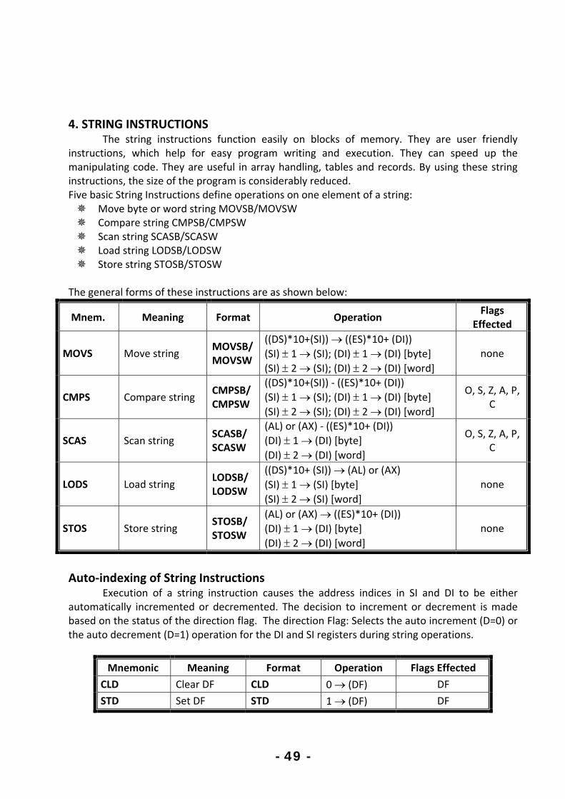
4. STRING INSTRUCTIONS The string instructions function easily on blocks of memory. They are user friendly
instructions, which help for easy program writing and execution. They can speed up the manipulating code. They are useful in array handling, tables and records. By using these string instructions, the size of the program is considerably reduced. Five basic String Instructions define operations on one element of a string: Move byte or word string MOVSB/MOVSW Compare string CMPSB/CMPSW Scan string SCASB/SCASW Load string LODSB/LODSW Store string STOSB/STOSW
The general forms of these instructions are as shown below:
Mnem. Meaning Format Operation Flags
Effected
MOVS Move string MOVSB/ MOVSW
((DS)*10+(SI)) ((ES)*10+ (DI))
(SI) 1 (SI); (DI) 1 (DI) [byte]
(SI) 2 (SI); (DI) 2 (DI) [word]
none
CMPS Compare string CMPSB/ CMPSW
((DS)*10+(SI)) ‐ ((ES)*10+ (DI))
(SI) 1 (SI); (DI) 1 (DI) [byte]
(SI) 2 (SI); (DI) 2 (DI) [word]
O, S, Z, A, P, C
SCAS Scan string SCASB/ SCASW
(AL) or (AX) ‐ ((ES)*10+ (DI))
(DI) 1 (DI) [byte]
(DI) 2 (DI) [word]
O, S, Z, A, P, C
LODS Load string LODSB/ LODSW
((DS)*10+ (SI)) (AL) or (AX)
(SI) 1 (SI) [byte]
(SI) 2 (SI) [word]
none
STOS Store string STOSB/ STOSW
(AL) or (AX) ((ES)*10+ (DI))
(DI) 1 (DI) [byte]
(DI) 2 (DI) [word]
none
Auto‐indexing of String Instructions
Execution of a string instruction causes the address indices in SI and DI to be either automatically incremented or decremented. The decision to increment or decrement is made based on the status of the direction flag. The direction Flag: Selects the auto increment (D=0) or the auto decrement (D=1) operation for the DI and SI registers during string operations.
Mnemonic Meaning Format Operation Flags Effected
CLD Clear DF CLD 0 (DF) DF
STD Set DF STD 1 (DF) DF

- 50 -
Prefixes and the String Instructions In most applications, the basic string operations must be repeated in order to process
arrays of data. Inserting a repeat prefix before the instruction that is to be repeated does this, the repeat prefixes of the 8086 are shown in table below. For example, the first prefix, REP, caused the basic string operation to be repeated until the contents of register CX become equal to 0. Each time the instruction is executed, it causes CX to be tested for 0. If CX is found not to be 0, it is decremented by 1 and the basic string operation is repeated. On the other hand, if it is 0, the repeat string operation is done and the next instruction in the program is executed, the repeat count must be loaded into CX prior to executing the repeat string instruction.
Mnemonic Used with Meaning
REP MOVS STOS LODS
Repeat while not end of string CX ≠ 0
REPE/REPZ CMPS SCAS
Repeat while not end of string and strings are equal CX ≠ 0 & ZF = 1
REPNE/REPNZ CMPS SCAS
Repeat while not end of string and strings are not equal CX ≠ 0 & ZF = 0
Example 1: Write a program loads the block of memory locations from 0A000H through 0A00FH with number 5H. Solution:
MOV AX, 0H MOV DS, AX MOV ES, AX MOV AL, 05 MOV DI, A000H MOV CX, 0FH CLD
AGAIN: STOSB LOOP AGAIN
Example 2: write a program to copy a block of 32 consecutive bytes from the block of memory locations starting at address 2000H in the current Data Segment(DS) to a block of locations starting at address 3000H in the current Extra Segment (ES). Solution:
CLD MOV AX, data_seg MOV DS, AX MOV AX, extra_seg MOV ES, AX

- 51 -
MOV CX, 20H MOV SI, 2000H MOV DI, 3000H MOVSB REP
Example 3: Write a program that scans the 70 bytes start at location D0H in the current Data Segment for the value 45H, if this value is found replace it with the value 29H and exit scanning. Solution:
MOV AX,data‐seg MOV DS, AX CLD MOV DI, 00D0H MOV CX, 0046H MOV AL, 45H REPNE SCASB DEC DI MOV [DI], 29H HLT
Example 4: Write a program to move a block of 100 consecutive bytes of data starting at offset address 400H in memory to another block of memory locations starting at offset address 600H. Assume both block at the same data segment F000H. Use loop instructions. Solution :
MOV CX, 64H MOV AX, F000H MOV DS, AX MOV ES, AX MOV SI, 400H MOV DI, 600H CLD
NXTPT: MOVSB LOOP NXTPT HTL
Example 5: Explain the function of the following sequence of instructions
MOV DL, 05 MOV AX, 0A00H MOV DS, AX MOV SI, 0 MOV CX, 0FH

- 52 -
AGAIN: INC SI CMP [SI], DL LOOPNE AGAIN
Solution: The first 5 instructions initialize internal registers and set up a data segment the loop in the program searches the 15 memory locations starting from Memory location A001H for the data stored in DL (05H). As long as the value In DL is not found the zero flag is reset, otherwise it is set. The LOOPNE Decrements CX and checks for CX=0 or ZF =1. If neither of these conditions is met the loop is repeated. If either condition is satisfied the loop is complete. Therefore, the loop is repeated until either 05 is found or all locations in the address range A001H through A00F have been checked and are found not to contain 5. Example 6: Implement the previous example using SCAS instruction. Solution:
MOV AX, 0H MOV DS, AX MOV ES, AX MOV AL, 05 MOV DI, A001H MOV CX, 0FH CLD
AGAIN: SCASB LOOPNE AGAIN

- 53 -
5. CONTROL TRANSFER INSTRUCTIONS These instructions transfer the program control from one address to other address. (Not
in a sequence). They are again classified into four groups. They are:
Unconditional Transfer Instructions
Conditional Transfer Instructions
Iteration Control Instructions
Interrupt Instructions
JMP CALL RET
JA / JNBE JAE / JNB JB / JNAE JBE / JNA JC JE / JZ JG / JNLE JGE / JNL JL / JNGE
JLE / JNG JNC JNE / JNZ JNO JNP / JPO JNS JO JP / JPE JS
LOOP LOOPE / LOOPZ LOOPNE / LOOPNZ
INT INTO IRET
5.1 JUMP Instruction 8086 allowed two types of jump operation. They are the unconditional jump and the
conditional jump. 5.1.1 Unconditional jump:
JMP (Jump) unconditionally transfers control from one code segment location to another. These locations can be within the same code segment (near control transfers) or in different code segments (far control transfers). There are two basic kinds of unconditional jumps:
1. Intrasegment Jump: is limited to addresses within the current code segment. This type of jump is achieved by just modifying the value in IP.
2. Intersegment Jump: permit jumps from one code segment to another. Implementation of this type of jump requires modification of the contents of both CS and IP.
1. Intrasegment Jump
bit 8 LableShort
bit 16 LableNear
reg.IP 16gptrRe
M.L ofcontent IP 16Memptr
2. Intersegment Jump
bit 16 ondsecCS
bit 16 firstIP LableFar
byte 2 ondsec of contentCS
byte 2 first of contentIP Memptr

- 54 -
Example 1: Assume the following state of 8086: (CS)=1075H, (IP)=0300H, (SI)=A00H, (DS)=400H, (DS:A00)=10H, (DS:A01)=B3H, (DS:A02)=22H, (DS:A03)=1AH. To what address is program control passed if each of the following JMP instruction is execute?
(a) JMP 85 1075:85 Short jump
(b) JMB 1000H 1075:1000 Near jump
(c) JMP [SI] 1075: B310 Near jump
(d) JMP SI 1075: 0A00 Near jump
(e) JMP FAR [SI] 1A22: B310 Far jump
(f) JMP 3000:1000 3000:1000 Far jump 5.1.2 Conditional Jump
The conditional jump instructions test the following flag bits: S, Z, C, P, and O. If the condition under test is true, a branch to the label associated with jump instruction occurs. If the condition is false, the next sequential step in the program executes. Tables below are a list of each of the conditional jump instructions.
Table1: Unsigned Conditional Transfers
Mnemonic Meaning “Jump if….. ” Condition Tested
JA/JNBE above/not below nor equal (CF or ZF) = 0
JAE/JNB above or equal/not below CF = 0
JB/JNAE below/not above nor equal CF = 1
JBE/JNA below or equal/not above (CF or ZF) = 1
JC Carry CF = 1
JE/JZ equal/zero ZF = 1
JNC not carry CF = 0
JNE/JNZ not equal/not zero ZF = 0
JNP/JPO not parity/parity odd PF = 0
JP/JPE parity/parity even PF = 1
JCXZ CX register is zero CF or ZF = 0
Table2: Signed Conditional Transfers
Mnemonic Meaning “Jump if….. ” Condition Tested
JG/JNLE greater/not less nor equal ((SF xor OF) or ZF) = 0
JGE/JNL greater or equal/not less (SF xor OF) = 0
JL/JNGE less/not greater nor equal (SF xor OF) = 1
JLE/JNG less or equal/not greater ((SF xor OF) or ZF) = 1
JNO not overflow OF = 0
JNS not sign (positive, including 0) SF = 0
JO Overflow OF = 1
JS sign (negative) SF = 1

- 55 -
Example 2: Write a program to move a block of 100 consecutive bytes of data string at offset address 8000H in memory to another block of memory location starting at offset address A000H. Assume that both blocks are in the same data segment value 3000H. Solution:
MOV AX, 3000H MOV DS, AX MOV SI, 8000H MOV DI, A000H MOV CX, 64H NXT: MOV AH, [SI] MOV [DI], AH INC SI INC DI DEC CX JNZ NXT HLT
Example 3: Write a program to add (50)H numbers stored at memory locations start at 4400:0100H , then store the result at address 200H in the same data segment. Solution:
MOV AX , 4400H MOV DS , AX MOV CX , 0050H�counter MOV BX , 0100H� offset
Again: ADD AL, [BX] INC BX label DEC CX JNZ Again MOV [0200], AL
5.2 CALL and RET Instructions A subroutine is a special segment of program that can be called for execution form any
point in program. There two basic instructions for subroutine : CALL and RET CALL instruction is used to call the subroutine. RET instruction must be included at the end of the subroutine to initiate the return
sequence to the main program environment. Just like the JMP instruction, CALL allows implementation of two types of operations: the
intrasegment call and intersegment call. Every subroutine must end by executing an instruction that returns control to the main
program. This is the return (RET). The operand of the call instruction initiates an intersegment or intrasegment call The intrasegment call causes contents of IP to be saved on Stack. The Operand specifies new value in the IP that is the first instruction in the subroutine.

- 56 -
The Intersegment call causes contents of IP and CS to be saved in the stack and new values to be loaded in IP and CS that identifies the location of the first instruction of the subroutine.
Execution of RET instruction at the end of the subroutine causes the original values of IP and CS to be POPed from stack.
Example 4: CALL 1234h CALL BX CALL [BX] CALL DWORD PTR [DI]
Example5: write a procedure named Square that squares the contents of BL and places the result in BX. Solution: Square: PUSH AX
MOV AL, BL MUL BL MOV BX, AX POP AX RET
Example6: write a program that computes y = (AL)2 + (AH)2 + (DL)2 , places the result in CX. Make use of the SQUARE subroutine defined in the previous example. (Assume result y doesn’t exceed 16 bit) Solution:
MOV CX, 0000H MOV BL,AL CALL Square ADD CX, BX MOV BL,AH CALL Square ADD CX, BX MOV BL,DL CALL Square ADD CX, BX HLT

- 57 -
5.3 Iteration Control Instructions The 8086 microprocessor has three instructions specifically designed for implementing
loop operations. These instructions can be use in place of certain conditional jump instruction and give the programmer a simpler way of writing loop sequences. The loop instructions are listed in table below:
Mnemonic Meaning Format Operation
LOOP LOOP LOOP short‐label
(CX)←(CX)‐1 Jump to location defined by short‐label if (CX) ≠ 0; otherwise, execute next instruction
LOOPE/ LOOPZ
Loop while equal/ loop while zero
LOOPE/LOOPZ short‐label
(CX)←(CX)‐1 Jump to location defined by short‐label if (CX) ≠ 0; an d (ZF)=1; otherwise, execute next instruction
LOOPNE/ LOOPNZ
Loop while not equal/ loop while not zero
LOOPNE/LOOPNZ short‐label
(CX)←(CX)‐1 Jump to location defined by short‐label if (CX) ≠ 0; and (ZF)=0; otherwise, execute next instruction
Example: Write a program to move a block of 100 consecutive bytes of data starting at offset address 400H in memory to another block of memory locations starting at offset address 600H. Assume both block at the same data segment F000H. (Similar to the example viewed in lecture 6 at page 59). Use loop instructions. Solution:
MOV AX, F000H MOV DS, AX MOV SI, 0400H MOV DI, 0600H MOV CX, 64H
NEXTPT: MOV AH, [SI] MOV [DI], AH INC SI INC DI LOOP NEXTPT HLT
6. PROCESS CONTROL INSTRUCTIONS
These instructions are used to change the process of the Microprocessor. They change the process with the stored information. They are again classified into two groups. They are:
1. Flage Control Instructions 2. External Hardware Synchronization Instructions

- 58 -
6.1 Flag Control Instructions: These instructions directly affected the state of flags. Figure below shows these
instructions.
Mnemonic Meaning Format Operation Flags Effected
STC Set Carry Flag STC 1 (CF) CF
CLC Clear Carry Flag CLC 0 (CF) CF
CMC Complement Carry Flag CMC CFCF CF
STD Set Direction Flag STD 1 (DF) DF
CLD Clear Direction Flag CLD 0 (DF) DF
STI Set Interrupt Flag STI 1 (IF) IF
CLI Clear Interrupt Flag CLI 0 (IF) IF
Example: Write an instruction sequence to save the current contents of the 8086’s flags in the memory location pointed to by SI and then reload the flags with the contents of memory location pointed to by DI Solution:
LAHF MOV [SI], AH MOV AH, [DI] SAHF
Example: Clear the carry flag without using CLC instruction. Solution:
STC CMC
6.2 External Hardware Synchronization Instructions:
Mnemonic Meaning
HLT Halt processor
WAIT Wait for TEST pin activity
ESC Escape to external processor interface
LOCK Lock bus during next instruction
NOP No operation

Pin DiaFiguremode
Depegroup
The
agram of e (1) shows es:
The mitypically
The matypically
nding on thps.
The firsmode.
The sec
The thir
e 8086 M
8086 and the Pin dia
inimum moy used for s
aximum my used for lhe mode of
st are the s
cond are the
rd are the s
Microproc
Pin descrgram of 808
ode is selesmaller sing
mode is selearger multif operation
signal havin
e signals wh
signals havin
Fig. 1: Pin
- 59
cessor H
ription of 86. The 808
ected by apgle micropro
ected by aple micropn selected, t
ng common
hich have sp
ng special fu
n Diagram o
-
Hardware
8086 86 can be co
pplying logocessor sys
applying logrocessor sythe 8086 si
n functions
pecial funct
unctions for
of 8086
e Specific
onfigured to
gic 1 to thetems.
gic 0 to thystems. ignals can b
in minimum
ions for min
r maximum
cations
o work in ei
e MX/MN
he MX/MN
be categori
m as well a
nimum mod
mode.
ither of two
input. It
X input. It
zed in thre
as maximum
de.
o
is
is
ee
m

- 60 -
Minimum mode Operation Figure (2) show block diagram of minimum mode. Minimum mode operation is the least expensive way to operate the 8086. In minimum mode, the 8086 itself provides all the control signals needed to implement the
memory and I/O interfaces. These control signals are identical to those of the Intel 8085A an earlier 8‐bit microprocessor. This mode allows the 8085A peripherals to be used with the 8086 without any special
consideration.
Maximum mode Operation Figure (3) show block diagram of maximum mode. This mode supports existence of more than one processor in a system i.e. multiprocessor
system. In a multiprocessor system environment more than one processor exists in the system, and
each processor is executing its own program. In maximum mode the 8086 provides facilities by generating some of the control signals
externally.
In maximum‐mode, a separate chip (the 8288 Bus Controller) is used to help in sending control signals over the shared bus.
Address / data bus
8086 MPU
Power supply
Vcc GND
INTR
_____ INTA
_____ TEST
NMI
RESET
HOLD
HLDA
’⁄
AD0-AD15, A16/S3-A19/S6
ALE ____
BHE/S7
DT/
___ RD ___ WR
____ DEN
READY
CLK
DMA
Interface
Memory/IO Controls
Mode Select MN/
Interrupt Interface
Fig. 2: Minimum mode block diagram of 8086

The siggnals com
Nam
AD15‐AD0
A19/S6 ‐ A
MX/MN
RD
TEST
READY RESET
CLK
Vcc
GND
BHE/S7
INTR
NIM
mmon for b
me
0 A
A16/S3 A
M
R
W
W
S
S
+
G
B
I
n
Fig. 3:
both mini
Address/Da
Address/Sta
Minimum/M
Read Contro
Wait on test
Wait state c
System rese
System cloc
+5V
Ground
Bus High En
nterrupt Re
non maskab
: Maximum
- 61
imum & m
Common S
Function
ta Bus
atus
Maximum m
ol
t control
control
et
ck
nable/Status
equest
ble interrup
mode bloc
-
maximum
Signals
mode contro
s
t Request
ck diagram
modes:
Bidire
Outpu
ol Input
Outpu
Input
Input
Input
Input
Input
Input
Input
Input
Input
of 8086
Type
ctional , 3‐s
ut , 3‐state
ut , 3‐state
state
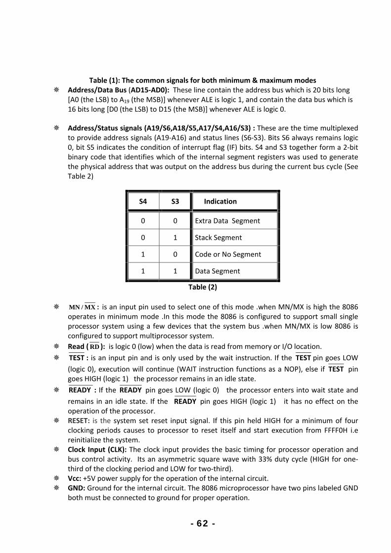
- 62 -
Table (1): The common signals for both minimum & maximum modes Address/Data Bus (AD15‐AD0): These line contain the address bus which is 20 bits long
[A0 (the LSB) to A19 (the MSB)] whenever ALE is logic 1, and contain the data bus which is 16 bits long [D0 (the LSB) to D15 (the MSB)] whenever ALE is logic 0.
Address/Status signals (A19/S6,A18/S5,A17/S4,A16/S3) : These are the time multiplexed to provide address signals (A19‐A16) and status lines (S6‐S3). Bits S6 always remains logic 0, bit S5 indicates the condition of interrupt flag (IF) bits. S4 and S3 together form a 2‐bit binary code that identifies which of the internal segment registers was used to generate the physical address that was output on the address bus during the current bus cycle (See Table 2)
S4 S3 Indication
0 0 Extra Data Segment
0 1 Stack Segment
1 0 Code or No Segment
1 1 Data Segment
Table (2)
MX/MN : is an input pin used to select one of this mode .when MN/MX is high the 8086 operates in minimum mode .In this mode the 8086 is configured to support small single processor system using a few devices that the system bus .when MN/MX is low 8086 is configured to support multiprocessor system.
Read (RD ): is logic 0 (low) when the data is read from memory or I/O location.
TEST : is an input pin and is only used by the wait instruction. If the TEST pin goes LOW
(logic 0), execution will continue (WAIT instruction functions as a NOP), else if TEST pin goes HIGH (logic 1) the processor remains in an idle state.
READY : If the READY pin goes LOW (logic 0) the processor enters into wait state and
remains in an idle state. If the READY pin goes HIGH (logic 1) it has no effect on the operation of the processor.
RESET: is the system set reset input signal. If this pin held HIGH for a minimum of four clocking periods causes to processor to reset itself and start execution from FFFF0H i.e reinitialize the system.
Clock Input (CLK): The clock input provides the basic timing for processor operation and bus control activity. Its an asymmetric square wave with 33% duty cycle (HIGH for one‐third of the clocking period and LOW for two‐third).
Vcc: +5V power supply for the operation of the internal circuit. GND: Ground for the internal circuit. The 8086 microprocessor have two pins labeled GND
both must be connected to ground for proper operation.

- 63 -
Bus High Enable/Status (BHE/S7): The bus high enable signal goes low to indicate the transfer of data over the higher order (D15-D8). The state S7 is always logic 1.
Interrupt Request (INTR) : is a maskable interrupt input. This is a triggered input. This is sampled during the last clock cycles of each instruction to determine the availability of the request. If any interrupt request is pending (IF=1), the processor enters the interrupt
acknowledge cycle ( INTA becomes active) after the current instruction has complete execution.
NIM: is the non maskable interrupt input. The NMI is not maskable internally by software. A transition from low to high initiates the interrupt response at the end of the current instruction.
Minimum mode interface signals
Minimum mode Signals ( MX/MN =Vcc)
Name Function Type
(M/ IO ) Memory/IO Control Output , 3‐state
WR WRITE Control Output , 3‐state
ALE Address Latch Enable Output
RDT Data Transmit/Receive Output , 3‐state
DEN Data Enable Output , 3‐state
HOLD Hold request Input
HLDA Hold Acknowledgment Output
INTA Interrupt Acknowledgment Output
Table (3): Minimum mode Signals.
Memory/IO (M/ IO ): This is a status line logically equivalent to S2 in maximum mode. When it is LOW, it indicates the CPU is having an I/O operation, and when it is HIGH, it indicates that the CPU is having a memory operation.
WRITE (WR ): indicates that the processor is performing a write memory or write I/O cycle, depending on the state of the M/IO signal.
Interrupt Acknowledge ( INTA ): This signal is used as a read strobe for interrupt acknowledge cycles. i.e. when it goes low, the processor has accepted the interrupt.
Address Latch Enable (ALE) : It is an output signal provided by the 8086 and can be used to demultiplexed AD0 to AD15 in to A10 toA15 and D0 to D15. This signal is active high and is never tristated.
Data Transmit/Receive ( RDT ): This output is used to decide the direction of data flow
through the transceiver (bidirectional buffers). When ( RDT = 1) the processor sends
data out (transmitting), when ( RDT = 0) the processor receiving data.
Data Enable (DEN): activate external data bus buffers.

- 64 -
HOLD: When an external device wants to take control of the system bus (Data, Address, Control), it signals to the 8086 by switching HOLD to logic 1. The hold input requests a direct memory access (DMA).
Hold Acknowledge : The processor, after receiving the HOLD request, issues the hold acknowledge signal on HLDA pin, indicates that the 8086 has entered the hold.
Maximum mode interface signals
Maximum mode Signals ( MX/MN =GND)
Name Function Type
RQ /GT0 ,(RQ /GT1 ) Request/Grant bus access control Bidirectional
( S2 , S1 , S0 ) Status Lines Output , 3‐state
LOCK Bus priority lock control Output , 3‐state
QS1 , QS0 Queue Status Output
Table (4): Maximum mode Signals.
Request/Grant (RQ /GT0 ,(RQ /GT1 ): These lines are bidirectional, and are used to both
request and grant a DMA operation in maximum mode.
LOCK : This output pin indicates that other system bus master will be prevented from gaining the system bus, while the LOCK signal is low. The LOCK signal is activated by the ‘LOCK’ prefix instruction and remains active until the completion of the next instruction.
Status Lines ( S2 , S1 , S0 ): These three bit are input to the external bus controller device 8288, which decodes them to identify the type of next bus cycle. Table (5) shows the function of these status bits in maximum mode.
S2 S1 S0 CPU Cycle 8288 Command
0 0 0 Interrupt Acknowledge INTA
0 0 1 Read I/O port IORC
0 1 0 Write I/O port IOWC , AIOWC
0 1 1 Halt None
1 0 0 Code Access MRDC
1 0 1 Read Memory MRDC
1 1 0 Write Memory AMWCMWTC,
1 1 1 Passive None
Table (5): Bus Status Codes

- 65 -
Queue Status (QS1, QS2): provide status to allow external tracking of the internal 8086 instruction queue. These pins are provided for access by the numeric coprocessor (8087). Table (6) shows the operation of the queue status bits.
QS1 QS0 Indication
0 0 No Operation (Queue is idle)
0 1 First Byte of the opcode from the queue
1 0 Empty Queue
1 1 Subsequent Byte from the Queue
Table (6): Queue Status bits
SYSTEM CLOCK To synchronize the internal and external operations of the microprocessor a clock (CLK)
input signal is used. The CLK can be generated by the 8284 clock generator IC. The 8086 is manufactured in three speeds: 5 MHz, 8 MHz and 10 MHz. For 8086, we connect either a 15‐, 24‐ or 30‐MHz crystal between inputs X1 and X2 of the
clock chip (see Fig. 4). The fundamental crystal frequency is divided by 3 within the 8284 to give either a 5‐, 8‐ or
10‐MHz clock signal, which is directly connected to the CLK input of the 8086.
Bus cycle and time state
A bus cycle defines the basic operation that a microprocessor performs to communicate with external devices. Example of bus cycles are • Memory read • Memory write • IO read • IO write The bus cycle of 8086 microprocessors consists of at least four clock periods (T1, T2, T3, and T4) During T1 the 8086 puts an address on the bus. During T2 the 8086 puts the data on the bus (for write memory cycle) and maintained
through T3 and T4
Fig. 4: Connecting the 8284 to the 8086.

- 66 -
During T2 the 8086 puts the bus in high‐Z state (for read cycle) and then the data to read must be available on the bus during T3 and T4.
These four clock states give a bus cycle duration of 125 ns × 4= 500 ns in an 8‐MHz system.
Idle States If no bus cycles are required, the microprocessor performs what are known as idle state.
During these states, no bus activity takes place. Each idle state is one clock period long, and any number of them can be inserted between bus cycles. Idle states are performed if the instruction queue inside the microprocessor is full and it does not need to read or write operands form memory.
Wait States
Wait states can be inserted into a bus cycle. This is done in response to request by an event in external hardware instead of an internal event such as a full queue. The READY input of the 8086 is provided specifically for this purpose. As long as READY is held at the 0 level, wait states are inserted between states T3 and T4 of the current bus cycle, and the data that were on the bus during T3 are maintained. The bus cycle is not completed until the external hardware returns READY back to the 1 logic level.
Read Cycle The read bus cycle begins with state T1. During this period, the 8086 output the 20bit
address of the memory location to be accessed on its multiplexed address/data bus AD0 through AD15 and multiplexed lines A16/S3 through A19/S6. Note that at the same time a pulse is also
produced at ALE. The signal BHE is also supplied with the address lines. (Figure 5 )
Write Cycle
The write bus cycle is similar to the read bus cycle except that signal WR instead of the
signal RD and signal RDT is set to 1.

- 67 -
Fig. 5: Minimum‐mode memory read bus cycle of the 8086.

68
The 8086 Memory Interface
Memory Devices Simple or complex, every microprocessor‐based system has a memory system. Almost all systems contain four common types of memory:
Read only memory (ROM) Flash memory (EEPROM) Static Random access memory (SARAM) Dynamic Random access memory (DRAM).
Before attempting to interface memory to the microprocessor, it is essential to understand the operation of memory components.
Memory Pin Connections
Figure (1) shows a general form diagram of ROM and RAM pins. Pin connections common to all memory devices are:
Address connections
Data connections
Selection connections
Control connections Address connections: All memory devices have address inputs that select a memory location within the memory device. Address inputs are labeled from A0 to An Data connections: All memory devices have a set of data outputs or input/outputs. Today many of them have bi‐directional common I/O pins. Selection connections: Each memory device has an input that selects or enables the memory
device. This kind of input is most often called a chip select ( CS ), chip enable (CE ) or simply
select ( S ) input.
RAM memory generally has at least one CS or S input and ROM at least one CE .
If the CE , CS , S input is active the memory device perform the read or write.
If it is inactive the memory device cannot perform read or write operation.
If more than one CS connection is present, all most be active to perform read or write data.
Control connections:
A ROM usually has only one control input, while a RAM often has one or two control inputs.
The control input most often found on the ROM is the output enable ( OE ) or gate ( G ), this allows data to flow out of the output data pins of the ROM.

69
A RAM memory device has either one or two control inputs. If there is one control input it
is often called WR .
This pin selects a read operation or a write operation only if the device is selected by the
selection input ( CS )
Read‐only memory (ROM) Read‐only memory (ROM) permanently stores programs/data resident to the system, and
must not change when power disconnected Often called nonvolatile memory, because its contents do not change even if power is
disconnected. A device we call a ROM is purchased in mass quantities from a manufacturer.
programmed during fabrication at the factory The EPROM (erasable programmable read‐only memory) is programmed in the field on a
device called an EPROM programmer. Also erasable if exposed to high‐intensity ultraviolet light, depending on the type of
EPROM. The PROM (programmable read‐only memory) is also programmed in the field by burning
open tiny NIchrome or silicon oxide fuses. Once it is programmed, it cannot be erased. A newer type of read‐mostly memory (RMM) is called the flash memory. Flash memory is also often called an EEPROM (electrically erasable programmable ROM)
or EAROM (electrically alterable ROM) or a NOVRAM (nonvolatile RAM) Electrically erasable in the system, but they require more time to erase than normal RAM. The flash memory device is used to store setup information for systems such as the video
card in the computer.
Fig. 1: Memory Component

70
Static Random Access Memory (SRAM) A Static RAM is a volatile memory device which means that the contents of the memory
array will be lost if power is removed. Unlike a dynamic memory device, the static memory does not require a periodical refresh
cycle and generally runs much faster than a dynamic memory device. Static RAM is used when the size of the read/write memory is relatively small, today, a
small memory is less than 1M byte. The main difference between ROM and RAM is that RAM is written under normal
operation, whereas ROM is programmed outside the computer and normally is only read.
Dynamic Random Access Memory (DRAM) Available up to 256M X 8 (2G bits). DRAM is essentially the same as SRAM, except that it retains data for only 2 or 4 ms on an
integrated capacitor. After 2 or 4 ms, the contents of the DRAM must be completely rewritten (refreshed),
because the capacitors, which store a logic 1 or logic 0, lose their charges.
8086 Memory Interface The memory address space of the 8086‐based microcomputers has different logical and
physical organizations (see Fig. 2).
Logically, memory is implemented as a single 1M × 8 memory chunk. The byte‐wide
storage locations are assigned consecutive addresses over the range from 00000H through FFFFFH
Physically, memory is implemented as two independent 512 Kbyte banks: the low (even) bank and the high (odd) bank. Data bytes associated with an even address (00000H,
Fig. 2: (a) Logical memory organization, and (b) Physical memory organization (high and low memory banks) of the 8086 microprocessor.
(a) (b)

71
00002H, etc.) reside in the low bank, and those with odd addresses (00001H, 00003H, etc.) reside in the high bank.
Address bits A1 through A19 select the storage location that is to be accessed. They are
applied to both banks in parallel. A0 and bank high enable (BHE ) are used as bank‐select signals.
The memory locations 00000‐FFFFF are designed as odd and even bytes. To distinguish
between odd and even bytes, the CPU provides a signal called BHE (bus high enable).
BHE and A0 are used to select the odd and even byte, as shown in the table below.
BHE A0 Function
0 0 Choose both odd and even memory bank
0 1 Choose only odd memory bank
1 0 Choose only even memory bank
1 1 None is chosen
Minimum mode Memory Interface Figure (3) show block diagram of minimum mode 8086 memory interface.
The control signals provided to support the interface to the memory subsystem are
ALE , IOM , RDT , RD , WR , DEN and BHE
When Address latch enable (ALE) is logic 1 it signals that a valid address is on the bus. This address can be latched in external circuitry on the 1‐to‐0 edge of the pulse at ALE.
IOM (memory/IO) and RDT tells external circuitry whether a memory or I/O transfer
is taking place over the bus, and whether the 8086 will transmit or receive data over the bus.
Fig. 3: Minimum mode memory interface
8086MPU
MemorySubsystem
and bus interfaceCircuit
ALE
AD0-AD15
RD
WR
M/IO
DT/R
DEN
BHEMN/MX
Vcc

72
The bank high enable (BHE ) signal is used as a memory enable signal for the most significant byte half of the data bus, D8 through D15.
The signals WR (write) and RD (read) identify that a write or read bus cycleis in progress.
DEN (data enable), is also supplied. It enables external devices to supply data to the microprocessor.
Maximum mode Memory Interface Figure (4) show block diagram of maximum mode memory interface. In maximum mode the 8086 not directly provides all control signal to support the
memory interface. Instead, an external Bus Controller (8288) provides memory commands and control
signals as shown in table (5) in lecture (8).
Memory expansion
In many applications, the microcomputer system requirement for memory is greater than what is available in a single device. There are two basic reasons for expanding memory capacity: 1. The byte‐wide length is not large enough 2. The total storage capacity is not enough bytes. Both of these expansion needs can be satisfied by interconnecting a number of ICs.
Fig. 4: Maximum mode memory interface
8086

73
Example 1: show how to implement 32K× 16 EPROM using two 32K×8 EPROM? Solution:
Example 2: Design 8086’s memory system consisting of 512K bytes of RAM memory and 128K bytes of ROM use the devices in figure below. RAM memory is to reside over the address range 00000H through 7FFFFH and the address range of the ROM is to be A0000H through BFFFFH
Example 3: Design 8086’s memory system consisting of 64K bytes of ROM memory, make use of the devices in figure below. The memory is to reside over the address range 60000H through 6FFFFH

74
Example 4: Design a 8086 memory system consisting of 1Mbytes, Using 64K× 8 memory. Solution:
Example5: show how to implement 64K× 8 EPROM using two 32K×8 EPROM?
Example5: show how to implement 32K× 32 EPROM using four 32K×8 EPROM?

75
The 8086 Input/output Interface
This lecture describes the IO interface circuits of an 8086‐based microcomputer system. The input/output system of the microprocessor allows peripherals to provide data or receive results of processing the data. This is done using I/O ports. 8088/8086 architecture implements independent memory and input/output address
spaces Memory address space‐ 1,048,576 bytes long (1M‐byte)—00000H‐FFFFFH Input/output address space‐ 65,536 bytes long (64K‐bytes)—0000H‐FFFFH Input/output can be implemented in either the memory or I/O address space Each input/output address is called a port The 8086 microcomputers can employ two different types of input/output (I/O):
Isolated I/O.
Memory‐mapped I/O.
Fig. (1): 8086 memory and I/O Interface
Isolated Input/output Using isolated I/O a microcomputer system, the I/O devices are treated separate from
memory. The part of the I/O address space from address 0000H through 00FFH is referred to as
Page 0 as shown in figure (2). Supports byte and word I/O ports 64K independent byte‐wide I/O ports 32K independent aligned word‐wide I/O ports

76
Advantages of isolated I/O 1. Complete memory address space available for use by memory 2. Special instructions have been provided in the instruction set of the 8086 to
perform isolated I/O operation. This instructions tailored to maximize performance
Disadvantage of Isolated I/O
All inputs/outputs must take place between an I/O port and accumulator (AL or AX) register
Fig. (2): Isolated I/O port.
Memory‐mapped Input/output Memory mapped I/O—a part of the memory address space is dedicated to I/O devices
For Example: (E0000H‐E0FFFH) 4096 memory addresses assigned to I/O ports E0000H, E0001H, and E0002H correspond to byte wide ports 0,1, and 2 E0000H and E0001H correspond to word‐wide port 0 at address E0000H Advantages of memory mapped I/O
1. Instructions that affect data in memory (MOV, ADD, AND, etc.) can be used to perform I/O operations
2. I/O transfers can take place between I/O port and any of the registers Disadvantage of memory mapped I/O
1. Memory instructions perform slower 2. Part of the memory address space cannot be used to implement memory

77
Fig. (3): Memory Mapped I/O port.
Differences between Isolated I/O and Memory Mapped I/O:
Isolated I/O No. Memory Mapped I/O
Isolated I/O uses separate memory space. 01 Memory mapped I/O uses memory from the main memory.
Limited instructions can be used. Those are IN, OUT, INS, OUTS.
02 Any instruction which references to memory can be used. (MOV, AND XCHG, SUB …….)
Faster because I/O instructions is specifically designed to run faster than memory instructions
03 Slower because memory instructions execute slower than the special I/O instructions
The memory address space is not affected 04 Part of the memory address space is lost
The addresses for Isolated I/O devices are called ports.
05 Memory mapped I/O devices are treated as memory locations on the memory map

78
Minimum Mode Interface Similar in structure and operation to memory interface I/O devices—can represent LEDs, switches, keyboard, serial communication port, printer
port, etc. I/O data transfers take place between I/O devices and MPU over the multiplexed‐address
data bus AD0‐AD7, A8‐A15 This interface use the control signals review
ALE = pulse to logic 1 tells bus interface circuitry to latch I/O address
RD = logic 0 tells the I/O interface circuitry that an input (read) is in progress
WR = logic 0 tells the I/O interface circuitry that an output (write) is in progress
IOM = logic 0 tells I/O interface circuits that the data transfer operation is for
the IO subsystem
RDT = sets the direction of the data bus for input (read) or output (write)
operation
DEN= enables the interface between the I/O subsystem and MPU data bus
Fig. (4): Minimum mode 8086 system I/O Interface.
Maximum Mode Interface Maximum‐mode interface differences review 8288 bus controller produces the control signals for I/O subsystem: Signal changes
IORC replaces RD
IOWC and AIOWC replace WR
DEN is complement of DEN
IOM no longer needed (bus controller creates separate IO read/write controls)
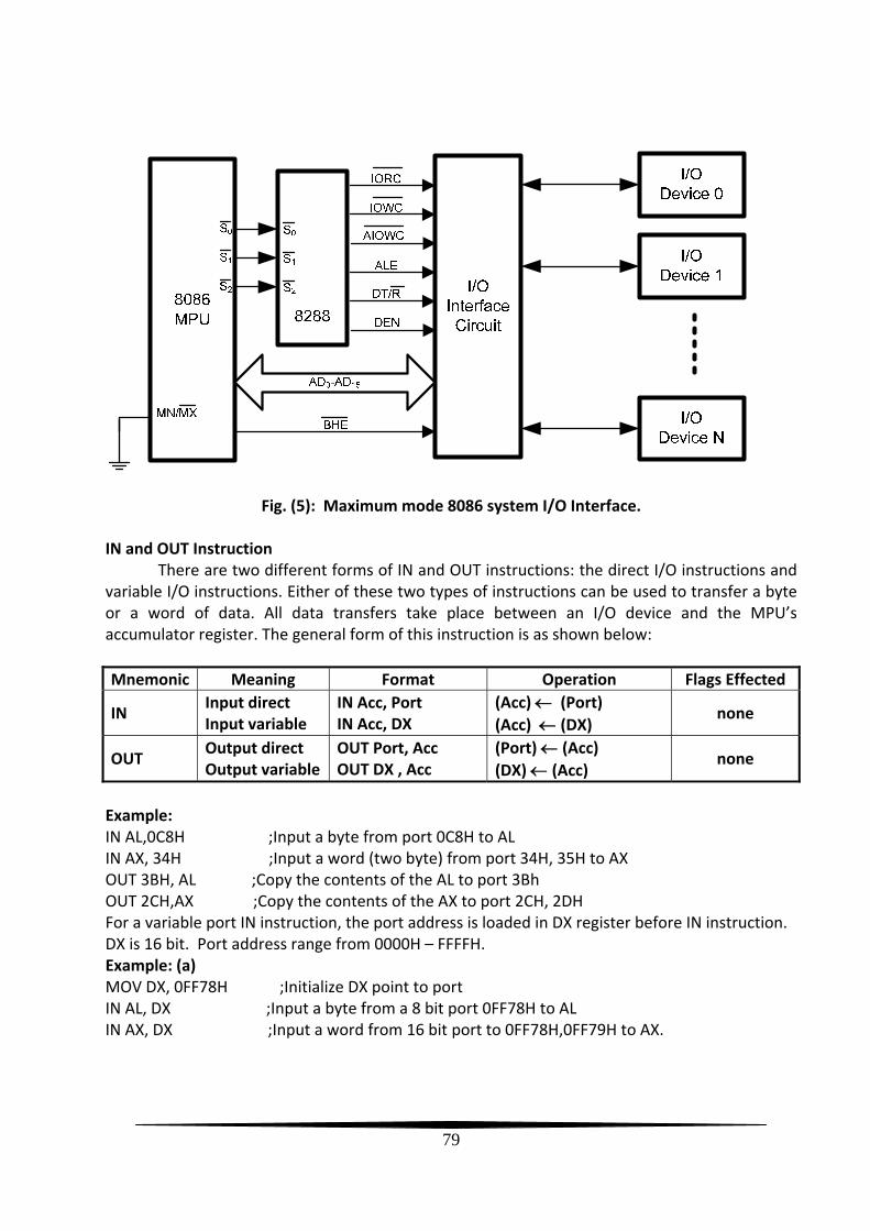
79
Fig. (5): Maximum mode 8086 system I/O Interface. IN and OUT Instruction
There are two different forms of IN and OUT instructions: the direct I/O instructions and variable I/O instructions. Either of these two types of instructions can be used to transfer a byte or a word of data. All data transfers take place between an I/O device and the MPU’s accumulator register. The general form of this instruction is as shown below:
Mnemonic Meaning Format Operation Flags Effected
IN Input direct Input variable
IN Acc, Port IN Acc, DX
(Acc) (Port)
(Acc) (DX) none
OUT Output direct Output variable
OUT Port, Acc OUT DX , Acc
(Port) (Acc)
(DX) (Acc) none
Example: IN AL,0C8H ;Input a byte from port 0C8H to AL IN AX, 34H ;Input a word (two byte) from port 34H, 35H to AX OUT 3BH, AL ;Copy the contents of the AL to port 3Bh OUT 2CH,AX ;Copy the contents of the AX to port 2CH, 2DH For a variable port IN instruction, the port address is loaded in DX register before IN instruction. DX is 16 bit. Port address range from 0000H – FFFFH. Example: (a) MOV DX, 0FF78H ;Initialize DX point to port IN AL, DX ;Input a byte from a 8 bit port 0FF78H to AL IN AX, DX ;Input a word from 16 bit port to 0FF78H,0FF79H to AX.

80
Example: write a series of instructions that will output FFH to an output port located at address B000H of the I/O address space. Solution:
MOV DX, B000H MOV AL, FF OUT DX, AL
Example: Data are to be read from two byte‐wide input ports at addresses AAH and A9H and then output as a word to a word‐wide output port at address B000H. Write a series of instructions to perform this input/output operation. Solution:
IN AL, AAH MOV AH, AL IN AL, A9H MOV DX, B000H OUT DX, AX
Input/Output Bus Cycles The input/output bus cycles are essentially the same as those involved in the memory
interface. Figure show the output bus cycle of the 8086. It’s similar to the write cycle except for
the signal IOM .
Fig. (6): Input bus cycle of 8086.

81
Fig. (7): Output bus cycle of 8086.
Byte‐Wide Input and Output Ports using Isolated I/O Figure (8) shows a circuits diagram of a byte‐wide input and output ports (8 bit) using isolated I/O for an 8086 based microcomputer system. From this diagram there is four parts:
Demultiplexing circuit: Two 74F373 octal latches are used to form a 16‐bit address latch. These devices latch the
address A0 through A15 synchronously with the ALE pulse. The latched address outputs are labeled AoL through A15L.
Remember that address lines A16 through A19 are not involved in the I/O interface. Data bus transceiver buffer in 8086 system is implemented using 74F245 octal bus IC’s,
where the control inputs ‘DIR ’ and ‘G ’ is used to control the data flow (An Bn) or
(Bn An). Figure (9) shows the block and circuit diagram of the 8‐bit Data bus transceiver buffer IC.
Also note thatG input is used to enable the buffer operation, whereas DIR input selects the direction of intended data transfer

82
Fig. (8): A byte‐wide input and output ports using Isolated I/P for an 8086 based.

83
Assume that the device is enabled by applyingG = 0. Now if DIR is set to logic 0, the output of AND gate 1 will be 0 and all the odd numbered buffers (G3, G5, G7 and so on) will be off. So the data path from An to Bn will be disabled. But the output of AND gate 2 will be logic 1 and all the even numbered buffers (G4, G6, G8 and so on) will be ON. Consequently, the data path from Bn to An will be ENABLED.
Similarly, forG = 0 and DIR = logic 1, data path from An to Bn will be ENABLED.
Fig. (9): The block and circuit diagram of the 8‐bit Data bus transceiver buffer IC.
Decoder circuit: A 74F138 (3 Line‐to‐ 8 Line decoder) is used for decoder circuit. Address lines A4L‐A15L are
applied to AND gate, output of AND gate and address line A0L provide two of the three enable inputs of the 74F138 input/output address decoder. These signals are applied to
enable input 1G and 2BG respectively.

84
The decoder requires one more enable signal at its 2AG input, which is supplied by the
complement of IOM .
The enable inputs must be 2BG 2AG 1G =001 to enable the decoder for operation.
The condition 2BG =0 corresponds to an even address, and 2AG =0 represent the fact that
an I/O bus cycle is in progress. 1G =1 is achieved if the output of AND gate is logic 1.
The three address lines L1L2L3 AAA are applied to select inputs CBA of the 74F138
decoder. When the decoder is enabled, the P output corresponding to these select inputs switches
to logic 0.
The Latch For output circuit we need to store the output data so we use latch, for this purpose
74F374 device is selected.
For Figure (8), the gate at the CLK input of 74F374 has its inputs P0 and WR .
When valid output data are on the bus, WR switches to logic 0. Since P0 is also 0, the CLK input of the 74F374 for port 0 switches to logic 0.
At the end of the WR pulse, the clock switches from 0 to 1, a positive transition. This causes the data on D0 –D7 to be latched and become available at output lines O0 –O7
of port 0
OE =0 enable the output , the latched data appears at the appropriate port outputs.
The Buffer Buffer is used with input ports. In figure (8) the 74F244 octal buffer is used to implement
the port. The outputs of the buffer are applied to the data bus for input to the MPU. This buffer has
three‐state outputs.
For Figure (8), the gate at the G input of 74F244 has its inputs P7 and RD .
When an input bus cycle is in progress, RD switches to logic 0. Since P7 is also 0, the G input of the 74F244 for port 7 switches to logic 0 and the outputs
of 74F244 are enabled. In this case, the logic levels at inputs I0 – I7 are passed onto data bus lines D0 – D7
respectively. This byte of data is carried through the enable data bus transceiver to the data bus of the
8086. As part of the input operation, the 8086 reads this byte of data into the AL register.
INPUT/OUTPUT Device The circuit in figure (8) has 8 LEDs attached to outputs O0 – O7 of output port 0. These
LEDs represent output device.

85
Also, in figure (8) there is 8 switches attached to input I0 – I7 of input port 7. These switches represent input device.
Example 1: For figure (8), what is the I/O address of
a. Port 0 (P0) b. Port 7 (P7)
Assume all unused address bit are at logic 0. Solution:
To enable ports P0 – P7 74F138 decoder must be enabled 2BG 2AG 1G =001
1G = 1 output of AND gate = 1 A4L – A15L = 111111111111
2BG = 0 A0L = 0
2AG = 0 IOM = 0
(a) To enable Port 0 (P0) :
Input of decoder ABC = 000 A1L A2L A3L = 000
A15L A14L A13L A12L A11L A10L A9L A8L A7L A6L A5L A4L A3L A2L A1L A0L
1 1 1 1 1 1 1 1 1 1 1 1 0 0 0 0
I/O address of Port 0 = FFF0H
(b) To enable Port 7 (P7) Input of decoder ABC = 111 A1L A2L A3L = 111
A15L A14L A13L A12L A11L A10L A9L A8L A7L A6L A5L A4L A3L A2L A1L A0L
1 1 1 1 1 1 1 1 1 1 1 1 1 1 1 0
I/O address of Port 0 = FFFEH Example 2: For the circuit of figure (8), write an instruction sequence that inputs the byte contents of input port 7 to the memory DS:A000H. Solution: The address of Port P7 =FFFEH. The instruction sequence needed to input the byte is: MOV DX, FFFEH IN AL, DX MOV [A000], AL
Example 3: For the circuit of figure (8), write an instruction sequence that outputs contents of memory location DS:8000H to output port 0. Solution: The address of Port P0 =FFF0H. The instruction sequence needed to output the contents of memory location DS:8000H to output port 0 is: MOV DX, FFF0H
MOV AL , [8000] OUT DX , AL

86
Time Delay Loop and Blinking an LED at an Output Port The circuit in Figure 1 show how to attach a LED to output port O7 of parallel port 0. The
port address is FFF0H, and the LED corresponds to bit 7 of the byte of data that is written to port 0. The circuit use 74LS374 (edge clocked octal latch).
For the LED to turn on, O7 must be switched to logic 0, and it will remain on until this output is switched back to 1. The 74LS374 is not an inverting latch, therefore, to make O7 logic 0, simply write 0 to that bit of the octal latch.
Fig. (1): Time Delay Loop and Blinking an LED at an Output Port
Example 1: Write instruction sequence to make the LED (in Figure 1) blink. Solution: we must write a program that first makes O7 logic 0 to turn on the LED, delays for a short period of time, and then switches O7 back to 1 to turn off the LED. This piece of program can run as a loop to make the LED continuously blink. This is done as follows: Sequence of instructions needed to initialize0 7 to logic 0.
MOV DX, FFF0H ; Initialize address of port0 MOV AL, 00H ; Load data with bit 7 as logic 0
ON_OFF: OUT DX, AL ; Output the data to port 0 Delay for a short period of time so as to maintain the data written to the LED
MOV CX, FFFFH ; Load delay count of FFFFH HERE: LOOP HERE ; Time delay loop The value in bit 7 of AL is complemented to 1 and then a jump is performed to return to the output operation that writes the data to the output port:
XOR AL, 80H ; Complement bit 7 of AL JMP ON_OFF ; Repeat to Output the new bit 7

87
Polling technique In practical applications, it is sometimes necessary within an I/O service routine to
repeatedly read the value at an input line and test this value for a specific logic level. Let us assume that we want to read the contents of port 0, and that input I3 at this port is
the line that is being polled. The circuit in Figure 2 show how to attach a switch to input port I2 of parallel port 0. The
port address is FFF0H, and the switch corresponds to bit2 of the byte of data that is read from port 0. The circuit use 74LS244 (unidirectional octal buffer).
It is common practice to poll a switch like this with software waiting for it to close. The instruction sequence that follows will poll the switch at I2 :
MOV CL, 03H MOV DX, FFF0H
POLL_I2: IN AL, DX SHR AL, CL JC POLL_I2 CONTINUE: ... ...
If the switch is open, then bit 2 in AL is 1 and this value is shifted into CF. The program will still loop until the switch is closed. If the switch closed, then the polling operation is complete and the instruction following the JC is executed.
Fig. (2): Reading the setting of switch connected to an input port.

88
Example: Write a sequence of instructions to read in the contents of ports 1 and port2 in the circuit shown in figure 2, and save them at consecutive memory addresses A0000H and A000H in memory. Solution:
MOV AX, A000H ; set up the segment to start at A000H MOV DS, AX MOV DX, FFF2H IN AL, DX ; input from port 1 MOV [0000H], AL ; save the input at A0000H MOV DX, FFF4 ; input form port 2 IN AL, DX MOV [0001H], AL ; save the input at A0001H
INPUT/OUTPUT HANDSHAKING AND A PARALLEL PRINTER INTERFACE In some applications, the microcomputer must synchronize the input or output of
information to a peripheral device. Two examples of interfaces that may require a synchronized data transfer are a serial
communications interface and a parallel printer interface. Sometimes it is necessary as part of the I/O synchronization process first to poll an input
from an I/O device and, after receiving the appropriate level at the poll input, to acknowledge this fact to the device with an output.
This type of synchronization is achieved by implementing what is known as handshaking as part of the input/output interface.
Conceptual view of the interface between the printer and a parallel printer port. There are three general types of signals at the printer interface: data, control, and status as shown in figure 3.
Fig. (3):

89
The printer is attached to the microcomputer system at a connector known as parallel printer port.
On a PC, a 25 pin connector is used to attach the printer. Figure 4 show the actual signals supplied at the pins of this connector are as shown below:
Figure (4‐a) shows a block diagram of a simple parallel printer interface. Here we find 8 data output lines, (D0‐D7), control strobe (STB), and statues signal busy (BUSY).
The MPU outputs data representing the character to be printed through the parallel printer interface.
Character data are latched at the outputs the parallel interface and are carried to the data inputs of the printer over data lines D0‐D7.
The STB output of the parallel printer interface is used to signal the printer that new character data are available.
Whenever the printer is already busy printing a character, it signals this fact to the MPU with the BUSY input of the parallel printer interface.
This handshake signal sequence is illustrated in figure (4‐b). Figure (4‐c) is a flow chart of a subroutine that performs a parallel printer interface
character‐transfer operation. The circuit in figure (5) implements the parallel printer interface in figure (4‐a).
Pin Assignment Pin Assignment
1 Strobe 10 Ack
2 Data 0 11 Busy
3 Data 1 12 Paper Empty
4 Data 2 13 Selection
5 Data 3 14 Auto Foxed
6 Data 4 15 Error
7 Data 5 16 Initialize
8 Data 6 17 Select in
9 Data 7 18‐25 Ground
8086MPU
ParallelPrinter
Interface
ALE
AD0-AD15
RD
WR
M/IO
DT/R
DEN
BHEMN/MX
Vcc
D0-D7
Printer
STB
BUSY
Fig. (4‐a): I/O interface that employ handshaking

90
Fig. (4‐b): Handshaking Signals
Fig. (4-c): Handshaking sequence flow chart

91
Example: Write a program that will implement the sequence in figure (4‐c) for circuit in figure (5). Character data are held in memory starting at address DS:3000, and the number of characters held in the buffer is identified by the count at address DS:6000. Solution:
MOV AX, DataSeg MOV DS, AX MOV CL , [6000]
; (CL) = character count
Setting
MOV SI , 3000 ; (SI) = character pointer
MOV DX, FFF4H ; Keep polling till busy=0
Busy check POLL‐BUZY: IN AL , DX AND AL , 01H JNZ POLL‐BUZY
MOV AL , [SI] ; Get the next character Data out MOV DX , FFF0H
OUT DX , AL And output it to port 0
MOV AL , 00H STB = 0
Strobe pulse
MOV DX , FFF2H OUT DX , AL STROBE: MOV BX , OFH Delay for STB duration DEC BX JNZ STROBE MOV AL , 01 STB = 1 OUT DX , AL
INC SI Update
DEC CL
JNZ POLL‐BUZY Repeat till all characters have been transferred Repeat
HLT
Fig. (5): Handshaking printer interface circuits

92

92
8255 Programmable Peripheral Interface (PPI) The 8255 is a widely used, programmable parallel I/O device. It can be programmed to
transfer data under data under various conditions, from simple I/O to interrupt I/O. It is flexible, versatile and economical (w hen multiple I/O ports are required). It is an important general purpose I/O device that can be used with almost any microprocessor. The 8255 has 24 I/O pins that can be grouped primarily into two 8 bit parallel ports: A and B, with the remaining 8 bits as Port C. The 8 bits of port C can be used as individual bits or be grouped into two 4 bit ports: CUpper (CU) and CLower (CL). The functions of these ports are defined by writing a control word in the control register.
Fig. (1): Pin layout of 8255 Programmable Peripheral Interface.
Control Logic of 8255
RD [READ]:‐ This control signal enables the read operation. When the signal is low, the microprocessor reads data from a selected I/O port of 8255
WR [WRITE]:‐ This control signal enables the write operation. When the signal goes low the MPU (microprocessor) writes into a selected I/O port or the control register.
RESET :‐ This is an active high signal, A logic high on this line clears the control word register and set all ports in the input mode. (that is , set as input port by default after reset)

93
CS [CHIP SELECT] :‐ This is a Chip Select line. If the line goes low it enables the 8255 to respond to RD and WR signals.
A1 – A0 :‐ These are address lines driven by the microprocessor. These address lines are used for selecting any one of the three ports or a control word.
CS A1 A0 Selected
0 0 0 Port A 0 0 1 Port B 0 1 0 Port C 0 1 1 Control Register 1 X X 8255 is not selected.
PA7 – PA0:‐ These are eight port A lines that act either as input or output lines depending up on the control word loaded into the control word register.
PC7 – PC4 : These are four Port C upper lines that can act as input or output lines. This port can be used for the generation of handshake lines.
PC3 – PCo: These are four port C lower lines that can act as input or output lines. This port can also be used for the generation of handshake lines.
PB0 – PB7: These are 8 port B lines which can be input or output lines in the same way as port A
D0 – D7: These are the data bus lines that carry data or control word to/from the microprocessor.
Fig. (2): Block diagram of 8255 Programmable Peripheral Interface.

94
CONTROL WORD REGISTER
The control register or the control logic or the command word register (CWR) is an 8‐bit register used to select the modes of operation and input/output designation of the ports.The figure below shows the register called the control register. The contents of this register called the control word specify an I/O function for each port that is the ports can function independently as input or output ports, which are achieved by the Control Word Register (CWR).
Bit D7 of the control register specifies the I/O function or the Bit Set/ Reset function. If the bit D7=1, bits D6‐D0 determine the I/O function in various modes. If bit D7=0, port C operates in the Bit Set/Reset (BSR) mode. The BSR control word does not affect functions of port A and B.
Fig. (3): 8255 Control Word Format.
To communication with peripherals through the 8255, three steps are necessary:
1. Determine the addresses of ports A, B and C and of the control register according to the Chip Select logic and the address lines A0 and A1.
2. Write a control word in the control register. 3. Write I/O instructions to communicate with the peripherals through ports A, B and C.
1 = I/O mode 0 = BSR mode

95
Operational modes of 8255
There are two basic operational modes of 8255:
1. Bit set/reset Mode (BSR Mode).
2. Input/Output Mode (I/O Mode).
The two modes are selected on the basis of the value present at the D7 bit of the Control Word Register. When D7 = 1, 8255 operates in I/O mode and when D7 = 0, it operates in the BSR mode
Bit set/reset (BSR) mode
The Bit Set/Reset (BSR) mode is applicable to port C only. Each line of port C (PC0 ‐ PC7) can be set/reset by suitably loading the control word register. BSR mode and I/O mode are independent and selection of BSR mode does not affect the operation of other ports in I/O mode.
D7 bit is always 0 for BSR mode. Bits D6, D5 and D4 are don't care bits. Bits D3, D2 and D1 are used to select the pin of Port C. Bit D0 is used to set/reset the selected pin of Port C.
As an example, if it is needed that PC5 be set, then in the control word,
1. Since it is BSR mode, D7 = '0'. 2. Since D4, D5, D6 are not used, assume them to be '0'. 3. PC5 has to be selected, hence, D3 = '1', D2 = '0', D1 = '1'. 4. PC5 has to be set, hence, D0 = '1'.
Thus, as per the above values, 0B (Hex) will be loaded into the Control Word Register (CWR).
D7 D6 D5 D4 D3 D2 D1 D0
0 0 0 0 1 0 1 1
Fig. (4): 8255 Control Word Format for BSR Mode.

96
Input/Output mode This mode is selected when D7 bit of the Control Word Register is 1. There are three I/O modes
1. Mode 0 ‐ Simple I/O 2. Mode 1 ‐ Strobed I/O 3. Mode 2 ‐ Strobed Bi‐directional I/O
For example, if port B and upper port C have to be initialized as input ports and lower port C and port A as output ports (all in mode 0):
1. Since it is an I/O mode, D7 = 1. 2. Mode selection bits, D2, D5, D6 are all 0 for mode 0 operation. 3. Port B and upper port C should operate as Input ports, hence, D1 = D3 = 1. 4. Port A and lower port C should operate as Output ports, hence, D4 = D0 = 0.
Hence, for the desired operation, the control word register will have to be loaded with 8A (hex).
Example 1: What is the mode and I/O configuration for ports A, B, C of an 82C55 after its
control register is loaded with 82 Solution:
Expressing the control register contents in binary form, we get:
D7 D6 D5 D4 D3 D2 D1 D0
1 0 0 0 0 0 1 0
D0 = 0 ; port C lower is an output
D1 = 1 ; port B is an input
D2 = 0 ; then Group B (port B and port C lower) is in mode 0
D3 = 0 ; port C upper is an output
D4 = 0 ; port A is an output port
D5 D6 = 0 ; then Group A (port A and port C upper) is in mode 0
D7 = 1 ; then mode set flag is active
Example 2: Write down 82C55 control word that set Port A, Port B and Port C lower as input
in mode 0, and set Port C upper as output in mode 0. Solution:
D0 = 1 ; port C lower is an input
D1 = 1 ; port B is an input
D2 = 0 ; then Group B (port B and port C lower) is in mode 0
D3 = 0 ; port C upper is an output
D4 = 1 ; port A is an output port
D5 D6 = 0 0 ; then Group A (port A and port C upper) is in mode 0
D7 = 1 ; then mode set flag is active
Then the control word contain 93H
D7 D6 D5 D4 D3 D2 D1 D0
1 0 0 1 0 0 1 1

97
Example 3: In 8086's8‐bit isolated I/O system, an 82C55 PPI is connected so that the address of
A, B, C ports, and Control register are 4D08H, 4D09H, 4D0AH and 4D0BH respectively. a) Draw the circuit diagram.
b) Write program to set Register A, B as input and Register C as output (all in mode 0). Then continuously receive two unsigned number from Registers A and B, compare them and output the larger to Register C.
Solution:
Then the control word contain 92H
D7 D6 D5 D4 D3 D2 D1 D0
1 0 0 1 0 0 1 0
The program
MOV AL, 92H MOV DX, 4D0BH OUT DX, AL
again: MOV DL, 08H (because DH is the same) IN AL,DX MOV BL, AL INC DL IN AL, DX

98
CMP AL, BL JNC no_exchange MOV AL, BL
no_exchange: INC DL OUT DX, AL MOV CX, FFFFH
delayloop: DEC CX JNZ delayloop JMP again
Mode 0: Simple Input or Output
This is also called basic I/O mode. In this mode, ports A and B are used as two simple 8‐bit I/O ports and port C as two 4‐bit ports. Each port (or half‐port in case of C) can be programmed to function as simply an input or an output port. The input/output features in Mode 0 as follows:
1. Output is latched.
2. Inputs are not latched.
3. Ports do not have handshake or interrupt capability.
4. Any port can be used as input or output port.
5. 4‐bit can combined used as a third 8‐bit port.
Mode 1: Input or Output with handshake
This is also called strobe I/O mode. In Mode 1: handshake signals are exchanged between the MPU and peripherals prior to data transfer. The features of this mode include the following:
1. Two ports (A and B) function as 8‐bit I/O ports. They can be configured either as input or output ports.
2. Each port uses three lines from port C as handshake signals. The remaining two lines of port C can be used for simple I/O functions.
3. Input and output data are latched.
4. Interrupt logic is supported.

99
Fig. (5): Mode 1 operation of 8255: Input or Output with handshake.
MODE 1: Input Control Signals The associated control signals are used for handshaking when ports A & B are configured as inputs. Port A uses PC3, PC4, PC5 and PC0, PC1, PC2. The functions of these signals are as follows: STB (Strobed input): This signal is generated by a peripheral device to indicate that it has transmitted a byte of data . The 8255, in response to this signal, generates IBF and INTR. IBF (input Buffer Full): This signal is an acknowledgement by the 8255A to indicate that it the input latch has received the data byte. This is reset when the MPU reads the data. INTR (Interrupt Request) :‐ This is an output signal that may be used to interrupt the MPU. This signal is generated if STB, IBF and INTE(Internal flip flop) are all at logic 1. this is reset by the falling edge of the RD Signal. INTE (Interrupt Enable): This is an internal flip flop used to enable or disable the generation of the INTR. The 2 flip flops INTEA and INTEB are set/reset using the BSR mode. The INTEA is enabled or disabled through PC4 and INTEB is enabled or disabled through PC2.
MODE 1: Output Control Signals The signals when port A & B are configured as output ports as follows: OBF (Output Buffer Full):‐ This is an output signal that goes low when the MPU writes data into the output latch of the 8255 A. This signal indicates to an output peripheral that new data are ready to be read. It goes high again after the 8255A receives an ACK from the peripheral. ACK (Acknowledge):‐ This is an input signal from a peripheral that must output a low when the peripheral receives the data from the 8255A ports.

100
INTR (Interrupt Request):‐ This is an output signal, and it is set by the rising edge of the acknowledge signal. This signal can be used to interrupt the MPU to request the next data byte for output. The INTR is set when OBF, ACK and INTE are all one and reset by the falling edge of WR. INTE (Interrupt Enable):‐ This is an internal flip flop to a port and needs to be set to generate the INTR signal. The two flip flops INTEA and INTEB are controlled by bits PC6 and PC2 respectively, through the BSR mode. PC4,5:‐ These two lines can be set up either as input or output.
Mode 2: Bidirectional Data Transfer
This is also called strobe bi‐directional I/O mode. This mode is used primarily in applications such as data transfer between two computers of floppy disk controller interface. In this mode,
Port A is programmed to be bi‐directional port
Port C is for handshaking
Port B can be either input or output in mode 0 or mode 1
Fig. (6): Mode 2 operation of 8255: Bidirectional Data Transfer.

101
Direct Memory Access (DMA):
Definition: A direct memory access (DMA) is an operation in which data is copied
(transported) from one resource to another resource in a computer system without
the involvement of the CPU.
The task of a DMA‐controller (DMAC) is to execute the copy operation of
data from one resource location to another. The copy of data can be performed
from:
I/O‐device to memory
memory to I/O‐device
memory to memory
I/O‐device to I/O‐device
Fig.1: Computer System with DMA
A DMA is an independent (from CPU) resource of a computer system added
for the concurrent execution of DMA‐operations. The first two operation modes
are ’read from’ and ’write to’ transfers of an I/O‐device to the main memory,
which are the common operation of a DMA‐controller. The other two operations
are slightly more difficult to implement and most DMA‐controllers do not
implement device to device transfers.

102
BASIC DMA OPERATION:
Two control signals are used to request and acknowledge a direct memory
access (DMA) transfer in the microprocessor‐based system.
The HOLD pin is an input used to request a DMA action.
The HLDA pin is an output that acknowledges the DMA action.
Figure 2 shows the timing that is typically found on these two DMA control pins.
Figure 2: HOLD and HLDA timing for the microprocessor.
HOLD is sampled in any clocking cycle
when the processor recognizes the hold, it stops executing software and
enters hold cycles
HOLD input has higher priority than INTR or NMI
the only microprocessor pin that has a higher priority than a HOLD is the
RESET pin
HLDA becomes active to indicate the processor has placed its buses at high‐
impedance state.
as can be seen in the timing diagram, there are
a few clock cycles between the time that HOLD changes and until HLDA
changes
DMA Controller • A DMA read causes the and signals to activate simultaneously.
• A DMA write causes the and signals to both activate.
• 8086 require a controller or circuit such as shown in Figure 3 for control bus
signal generation.

103
• The DMA controller provides memory with its address, and controller signal
( ) selects the I/O device during the transfer.
Fig. 3: A circuit that generates system control signals in a DMA environment.
• Data transfer speed is determined by speed of the memory device or a DMA
controller.
– if memory speed is 50 ns, DMA transfers occur at rates up to 1/50 ns
or 20 M bytes per second
– if the DMA controller functions at a maximum rate of 15 MHz with 50
ns memory, maximum transfer rate is 15 MHz because the DMA
controller is slower than the memory
– In many cases, the DMA controller slows the speed of the system
when transfers occur.

104
Fig. 4: DMA Controller
Internal Configuration of DMA
The DMA controller includes several registers:‐
The DMA Address Register contains the memory address to be used in the
data transfer. The CPU treats this signal as one or more output ports.
The DMA Count Register, also called Word Count Register, contains the no.
of bytes of data to be transferred. Like the DMA address register, it too is
treated as an O/P port (with a diff. Address) by the CPU.
The DMA Control Register accepts commands from the CPU. It is also
treated as an O/P port by the CPU.
Although not shown in figure (5), most DMA controllers also have a Status
Register. This register supplies information to the CPU, which accesses it as
an I/P port.

105
Fig. (5):Internal Configuration of DMA Controller
Process of DMA Transfer
To initiate a DMA transfer, the CPU loads the address of the first memory
location of the memory block (to be read or written from) into the DMA
address register. It does his via an I/O output instruction, such as the OTPT
instruction for the relatively simple CPU.
It then writes the no. of bytes to be transferred into the DMA count register
in the same manner.
Finally, it writes one or more commands to the DMA control register
These commands may specify transfer options such as the DMA transfer
mode, but should always specify the direction of the transfer, either from
I/O to memory or from memory to I/O.
The last command causes the DMA controller to initiate the transfer. The
controller then sets HOLD to 1 and, once HLDA becomes 1, seizes control of
the system buses

106
DMA Transfer Modes
1. BURST mode
Sometimes called Block Transfer Mode.
An entire block of data is transferred in one contiguous sequence.
Once the DMA controller is granted access to the system buses by the
CPU, it transfers all bytes of data in the data block before releasing
control of the system buses back to the CPU.
2. CYCLE STEALING Mode
Viable alternative for systems in which the CPU should not be disabled
for the length of time needed for Burst transfer modes.
3. TRANSPARENT Mode
This requires the most time to transfer a block of data, yet it is also
the most efficient in terms of overall system performance
Advantages of DMA
Computer system performance is improved by direct transfer of data
between memory and I/O devices, bypassing the CPU.
CPU is free to perform operations that do not use system buses.
Disadvantages of DMA
In case of Burst Mode data transfer, the CPU is rendered inactive for
relatively long periods of time.
THE 8237 DMA CONTROLLER
• The 8237 supplies memory & I/O with control signals and memory address
information during the DMA transfer.
• Actually a special‐purpose microprocessor whose job is high‐speed data
transfer between memory and I/O
• Figure 6 shows the pin‐out and block diagram of the 8237 programmable
DMA controller.

107
Fig. (6): The
8237A‐5 programmable DMA
controller. (a) Block
diagram and (b) pin‐out.

108
• 8237 is not a discrete component in modern microprocessor‐based systems
(it appears within many system controller chip sets).
• 8237 is a four‐channel device compatible with 8086/8088, adequate for
small systems (expandable to any number of DMA channel inputs).
• 8237 is capable of DMA transfers at rates up to 1.6M bytes per second. Each
channel is capable of addressing a full 64K‐byte section of memory and
transfer up to 64K bytes with a single programming
8237 Internal Registers
CAR: The current address register holds a 16‐bit memory address used for the
DMA transfer.
CWCR: The current word count register programs a channel for the number of
bytes (up to 64K) transferred during a DMA action. The number loaded into this
register is one less than the number of bytes transferred.
BA and BWC : The base address (BA) and base word count (BWC) registers are
used when auto‐initialization is selected for a channel. In auto‐initialization mode,
these registers are used to reload the CAR and CWCR after the DMA action is
completed.
CR: The command register programs the operation of the 8237 DMA controller.
MR: The mode register programs the mode of operation for a channel. Each
channel has its own mode register as selected by bit positions 1 and 0.
BR: The bus request register is used to request a DMA transfer via software
MRSR: The mask register set/reset sets or clears the channel mask.
MSR: The mask register clears or sets all of the masks with one command instead
of individual channels, as with the MRSR.
SR: The status register shows status of each DMA channel. The TC bits indicate if
the channel has reached its terminal count (transferred all its bytes). 34

109
Terminology
analog: continuously valued signal, such as temperature or speed, with infinite
possible values in between
digital: discretely valued signal, such as integers, encoded in binary
analog‐to‐digital: converter: ADC, A/D, A2D; converts an analog signal to a digital
signal
digital‐to‐analog: converter: DAC, D/A, D2A

- 1 -
Q1: Write a program to exchange two memory locations without using `xchg' instruction in assembly language.
DATA SEGMENT A DB 50H B DB 60H DATA ENDS CODE SEGMENT ASSUME DS:DATA,CS:CODE START: MOV AX,DATA MOV DS,AX MOV AL,A MOV AH,B MOV BL,AL MOV AL,AH MOV AH,BL MOV A,AL MOV B,AH MOV AX,4C00H INT 21H CODE ENDS