Embed Size (px)
Citation preview

CELL PHONE BASED VOTING SYSTEM ASIET,KALADY
CELL PHONE BASED VOTING SYSTEMCELL PHONE BASED VOTING SYSTEM
aMini Project report
Submitted in partial fulfillment of the requirements
for the award of B.Tech Degree in
Electronics & Communication Engineering
by
GOPIKRISHNA.B.WARRIER
APRIL 2010
Department of Electronics & Communication Engineering
ADI SHANKARA INSTITUTE OF ENGINEERING & TECHNOLOGY
(An ISO 9001:2008 Certified Institution)KALADY, KERALA
DEPT.OF ELECTRONICS&COMMUNICATION

CELL PHONE BASED VOTING SYSTEM ASIET,KALADY
ADI SHANKARA INSTITUTE OF ENGINEERING & TECHNOLOGY
(An ISO 9001:2008 Certified Institution) KALADY, KERALA
Certificate
Certified that this is the Bonafied Record of the mini Project entitled “Cell phone based voting system” submitted during the year 2010 in partial fulfillment for the award of Bachelor of Technology in Electronics & Communication Engineering under Mahatma Gandhi University.
Name: Gopikrishna.b.warrierRegister No: 56025Semester and branch: S6, Electronics & Communication Engineering
HOD In-charge
DEPT.OF ELECTRONICS&COMMUNICATION

CELL PHONE BASED VOTING SYSTEM ASIET,KALADY
Internal examiner External examinerPlace: KaladyDate:…./…./….
ACKNOWLEDGEMENT
It is with profound joy and immense pleasure that I place my gratitude and respect to all those
who have guided and inspired me for the project work.
I take this opportunity to extend my deep gratitude to Dr.S.G.Iyer, Principal, ASIET for granting
me permission to undertake this project. I also express my sincere thanks to Mr. Venugopal,
Head of the Department, Electronics and Communication Department, for giving me the
opportunity to utilize all resources for the completion of this project.
I am deeply indebted to my project guides,Mr. Bipin and Miss. Soumya of Electronics and
Communication Department for their guidance,timely advice and support rendered during all
stages of project work. I express my sincere gratitude to them. I extend my thanks to
Mrs.Sheeja.K.S, Lab assistant, for her valuable assistance during the course of my work.
Finally, I convey my thanks to my parents and friends who had directly or indirectly helped me
in the successful completion of this project.
Above all I thank God almighty who showered his blessings upon me in every lap of my life.
GOPIKRISHNA.B.WARRIER
DEPT.OF ELECTRONICS&COMMUNICATION

CELL PHONE BASED VOTING SYSTEM ASIET,KALADY
ABSTRACT
Using SMS Based Voting machine we can vote from our home just by sending a sms a specified
format from our mobile. The entire voters will be provided with a unique password (pin) and
identification number. For voting we have to send a sms in a predefined format. The voting
machine will receive this messages and decode the message and verify the the Pin number and
identification number if both number matches the voting machine will accept the vote else the
message is rejected by the machine.
The voting machine is implemented using pic microcontroller. A GSM MODEM is used to
receive messages from voters. The microcontroller accepts this message and verifies the message
and keep updates. A key is activated used to view the result. An LCD is used to display the
final result.
DEPT.OF ELECTRONICS&COMMUNICATION

CELL PHONE BASED VOTING SYSTEM ASIET,KALADY
CONTENTS
PAGE 1. Introduction 6
2. Proposed System Features 2.1 Block Diagram 72.2 Block Diagram Explanation
3. Hardware Implementation3.1 Circuit Diagram 20
3.2 Circuit Operation 21
4. PCB Design 4.1 Design of PCB 24 4.2 PCB Design And Fabrication 28
4.3 PCB Layout 38 4.4 PCB Component Layout 39
5. Conclusion and Future Enhancement 40
6. References 41
Appendix A 42 Appendix B 47 Appendix C 48
DEPT.OF ELECTRONICS&COMMUNICATION

CELL PHONE BASED VOTING SYSTEM ASIET,KALADY
INTRODUCTION
India is world’s largest democracy. Fundamental right to vote or simply voting in elections forms
the basis of Indian democracy. In India all earlier elections a voter used to cast his vote by using
ballot paper. This is a longtime-consuming process and very much prone to errors. This situation
continued till election scene was completely changed by electronic voting machine. No more
ballot paper, ballot boxes, stamping,etc.all this condensed into a simple box called ballot unit of
the electronic voting machine. Cell phone based voting machine is capable of saving
considerable printing stationery and transport of large volumes of electoral material. It is easy to
transport, store, and maintain. It completely rules out the chance of invalid votes. Its use results
reduction of polling time, resulting in fewer problems in electoral preparations, law and
order, candidates' expenditure,etc. and easy and accurate counting without any mischief at the
counting centre. The aim of our project is to design & develop a mobile based voting machine. In
this project user can dial the specific number from any land line or mobile phone to cast his
vote. Once the user is connected to the voting machine he can enter his password & choice of
vote. If he has entered a valid choice & password his vote will be caste with two short duration
beeps. For invalid password/choice long beep will be generated. User is allotted 15 seconds to
enter his password & choice. A reset button is provided for resetting the system. A total key is
provided to display the result
DEPT.OF ELECTRONICS&COMMUNICATION

CELL PHONE BASED VOTING SYSTEM ASIET,KALADY
BLOCK DIAGRAM
DEPT.OF ELECTRONICS&COMMUNICATION
PIC 16F876A
SERIALINTERFACE
GSM MODEM
MOBILE
LCD
KEY
CELL PHONE BASED VOTING SYSTEM ASIET,KALADY
BLOCK DIAGRAM EXPLANATION
PIC MICROCONTROLLERSMicrochip Technology Inc. is a leading provider of microcontroller and analog semiconductors,
providing low-risk product development, lower total system cost and faster time to market for
thousands of diverse customer applications worldwide.
PIC devices are grouped by the size of their instruction word length Classification
Base line: 12 bit instruction word length.Mid-range: 14 bit instruction word length. High-end: 16
bit instruction word length.
Each part of PIC can be placed into one of the three groups
Core
Peripherals
Special Features
The core includes the basic features that are required to make the device operate. These
include
Device Oscillator
Reset logic
CPU (Central Processing Unit) operation
ALU (Arithmetic Logical Unit) operation
Device memory map organization
Interrupt operation
Instruction set
Peripherals are the features that add a differentiation froma microprocessor. These include
General purpose I/O
Timer0
Timer1
Timer2
Capture, Compare, and PWM (CCP)
Synchronous Serial Port (SSP)
USART
DEPT.OF ELECTRONICS&COMMUNICATION

CELL PHONE BASED VOTING SYSTEM ASIET,KALADY
Analog to Digital (A/D) ConverterPeripherals
Special features are the unique features that help to
Decrease system cost
Increase system reliability
Increase design flexibility
The Mid-Range PIC offers several features such as
On-chip Power-on Reset (POR)
Brown-out Reset (BOR) logic
Watchdog Timer
Low power mode (Sleep)
In-Circuit Serial Programming™ (ICSP™)
Special Features
CPU Architectures….PIC16F876
PPPPPP PIC
PIC–Peripheral Interface Controller
16–Midrange series
F–Flash memory
873–28 pin,10bit adc, with internal EEPROM
DEPT.OF ELECTRONICS&COMMUNICATION

CELL PHONE BASED VOTING SYSTEM ASIET,KALADY
12–Base line
16–Midrange
17/18–High end
C–EPROM
CR–ROM
F–Flash
7X–28 pin,8bit adc, without internal EEPROM
87XX-28 pin,10bit adc, with internal EEPROM Naming of PIC
Core features
4K -Program memory
192 bytes -Data memory
128 bytes –EEPROM Data Memory
8-bit RISC ALU
Harvard architecture
28 pins with 22 I/O pins
I/O PORTSPORTS
A port is a group of pins on a microcontroller on which the desired combinations of zeros and
ones can be set simultaneously or the present status can be read.
PIC16F873 has 3 ports
PORTA -6 bit
PORTB -8 bit
PORTC -8 bit
TRIS REGISTERS
TRIS registers are control registers for ports
TRIS registers are in BANK1
TRISA control register for PORTA
TRISB control register for PORTB
TRISC control register for PORTC
If a bit of TRIS Register = 1,corresponding
PORT pin will be configured as input
DEPT.OF ELECTRONICS&COMMUNICATION

CELL PHONE BASED VOTING SYSTEM ASIET,KALADY
If a bit of TRIS Register = 0,corresponding
PORT pin will be configured as output
PORT A
PORTA is a 6-bit wide bi-directional port.
The corresponding data direction register is TRISA.
Setting a TRISA bit (=1) will make the corresponding PORTA pin an input
Clearing a TRISA bit (=0) will make the corresponding PORTA pin an output
Multiplexed with 5-channel 10-bit ADC(PA0, PA1, PA2, PA3, PA5)
PORT B
PORTB is an 8-bit wide, bi-directional port.
The corresponding data direction register is TRISB.
Setting a TRISB bit (=1) will make the corresponding PORTB pin an input
Clearing a TRISB bit (=0) will make the corresponding PORTB pin an output
Three pins of PORTB are multiplexed with the Low Voltage Programming function;
RB3/PGM, RB6/PGC and RB7/PGD.
Four of PORTB‟s pins, RB7:RB4, have an interrupt on change feature.
RB0/INT is an external interrupt input pin
Each of the PORTB pins has a weak internal pull-up. A single control bit can turn on all
the pull-ups.
PORT C
PORTC is an 8-bit wide, bi-directional port.
The corresponding data direction register is TRISC.
Setting a TRISC bit (=1) will make the corresponding PORTC pin an input
Clearing a TRISC bit (=0) will make the corresponding PORTC pin an output
INTERRUPTS
Interrupts are mechanisms of a microcontroller which makes it possible to respond to
some events at the moment when they occur, regardless of what microcontroller is doing
at the time.Each interrupt changes the flow of program execution, after executing an
interrupt subprogram (interrupt service routine) it continues from the same point .
DEPT.OF ELECTRONICS&COMMUNICATION

CELL PHONE BASED VOTING SYSTEM ASIET,KALADY
INTCONRBIF: RB Port Change Interrupt Flag bit1 = At least one of the RB7: RB4 pins
changed state 0 = None of the RB7: RB4 pins have changed state INTF: RB0/INT
External Interrupt Flag bit1 = The RB0/INT external interrupt occurred 0 = The RB0/INT
external interrupt did not occurT0IF: TMR0 Overflow Interrupt Flag bit1 = TMR0 has
overflowed 0 = TMR0 did not overflowRBIE: RB Port Change Interrupt Enable bit1 =
Enables the RB port change interrupt0 = Disables the RB port change interrupt
INTE: RB0/INT External Interrupt Enable bit
1 = Enables the RB0/INT external interrupt
0 = Disables the RB0/INT external interrupt
T0IE: TMR0 Overflow Interrupt Enable bit
1 = Enables the TMR0 interrupt
0 = Disables the TMR0 interrupt
PEIE: Peripheral Interrupt Enable bit
1 = Enables all peripheral interrupts
0 = Disables all peripheral interrupts
GIE: Global Interrupt Enable bit
1 = Enables all interrupts
0 = Disables all interrupts
TIMERS
PIC16F876 has 3 Timers
TIMER0 -8 bit
TIMER1 -16 bit
TIMER2 -8 bit
TIMER 0
TIMER 0
8-bit timer/counter
Readable and writable
8-bit software programmable prescaler
Interrupt on overflow from FFh to 00hTIMER 0 CONFIGURATION
Configure the OPTION REGISTER
DEPT.OF ELECTRONICS&COMMUNICATION

CELL PHONE BASED VOTING SYSTEM ASIET,KALADY
Load the count value
Wait for overflow flag to set
Clear the overflow flag
PS2:PS0: Prescaler Rate Select bits
PSA: Prescaler Assignment bit1 = Prescaler is assigned to the WDT0 = Prescaler is assigned to
the Timer0 moduleT0SE: TMR0 Source Edge Select bit1 = Increment on high-to-low transition
on T0CKI pin0 = Increment on low-to-high transition on T0CKI pinT0CS: TMR0 Clock Source
Select bit1 = Transition on T0CKI pin0 = Internal instruction cycle clock
(CLKOUT)INTEDGRBPU
OPTION_REGConfiguration Register BANK1TMR0Count Register
BANK0INTCON(2ndbit)Overflow Flag BANK0INTCON(5th bit)Interrupt Enable BANK0
TIMER1
Is a 16-bit timer consisting of two 8-bit registers (TMR1H and TMR1L)
The TMR1 Register pair (TMR1H:TMR1L) increments from 0000h to FFFFh
TMR1ON: Timer1 On bit1 = Enables Timer10 = Stops Timer1TMR1CS: Timer1 Clock Source
Select bit1 = External clock from pin RC0/T1OSO/T1CKI (on the rising edge)0 = Internal clock
(FOSC/4)T1SYNC: Timer1 External Clock Input Synchronization Control bitTMR1CS = 11 =
Do not synchronize external clock input0 = Synchronize external clock inputTMR1CS = 0This
bit is ignored. Timer1 uses the internal clock when TMR1CS = 0.
T1OSCEN: Timer1 Oscillator Enable Control bit1 = Oscillator is enabled0 = Oscillator is shut
offT1CKPS1:T1CKPS0: Timer1 Input Clock Prescale Select bits11 = 1:8 Prescale value10 =
1:4 Prescale value01 = 1:2 Prescale value00 = 1:1 Prescale valueUnimplemented: Read as ‟0‟
T1CON Configuration Register BANK0
TMR1L & TMR1HCount Register BANK0
PIR1 (0thBIT)Overflow Flag BANK0
PIE1 (0th BIT)Interrupt Enable BANK1
INTCONInterrupt Control BANK0
ER 2
TIMER 2
is an 8-bit timer with a prescaler and a postscaler.
DEPT.OF ELECTRONICS&COMMUNICATION

CELL PHONE BASED VOTING SYSTEM ASIET,KALADY
The Timer2 module has an 8-bit period register PR2.
Timer2 increments from 00h until it matches PR2 and then resets to 00h on the next increment
cycle.
T2CKPS1:T2CKPS0: Timer2 Clock Prescale Select bits
00 = Prescaler is 1
01 = Prescaler is 4
1x = Prescaler is 16
TMR2ON: Timer2 On bit
1 = Timer2 is on
0 = Timer2 is off
TOUTPS3:TOUTPS0: Timer2 Output Postscale Select bits
0000 = 1:1 Postscale
0001 = 1:2 Postscale
0010 = 1:3 Postscale
1111 = 1:16 Postscale
Unimplemented: Read as '0'
T2CON Configuration Register BANK0TMR2Count Register BANK0PR2Period Register
BANK1PIR1 (1st BIT)Overflow Flag BANK0PIE1 (1st BIT)Interrupt Enable
BANK1INTCONInterrupt Control BANK0
USARTUSART
The Universal Synchronous Asynchronous Receiver
Transmitter (USART) module is one of the two serial I/O modules. (USART is also known as a
Serial Communications Interface or SCI).
The USART can be configured as a full duplex asynchronous system that can communicate with
peripheral devices such as CRT terminals and personal computers.
TXST
TRANSMIT STATUS AND CONTROL REGISTER
TX9D: 9th bit of transmit data. Can be parity bit.TRMT: Transmit Shift Register Status bit1 =
TSR empty0 = TSR fullBRGH: High Baud Rate Select bitAsynchronous mode1 = High speed0
= Low speedSynchronous modeUnused in this modeUnimplemented: Read as '0
DEPT.OF ELECTRONICS&COMMUNICATION

CELL PHONE BASED VOTING SYSTEM ASIET,KALADY
SYNC: USART Mode Select bit
1 = Synchronous mode
0 = Asynchronous mode
TXEN: Transmit Enable bit
1 = Transmit enabled
0 = Transmit disabled
TX9: 9-bit Transmit Enable bit
1 = Selects 9-bit transmission
0 = Selects 8-bit transmission
CSRC: Clock Source Select bit
Asynchronous mode
Don‟t care
Synchronous mode
1 = Master mode (Clock generated internally from BRG)
0 = Slave mode (Clock from external source)
RECEIVE STATUS AND CONTROL REGISTER
RX9D: 9th bit of received data (Can be parity bit)CREN: Continuous Receive Enable
bitAsynchronous mode1 = Enables continuous receive0 = Disables continuous receiveSREN:
Single Receive Enable bitAsynchronous modeDon‟t careRX9: 9-bit Receive Enable bit1 =
Selects 9-bit reception0 = Selects 8-bit receptionSPEN: Serial Port Enable bit1 = Serial port
enabled 0 = Serial port disabled
SPBRG:Baud Rate Generator RegisterTXREG:Transmit BufferRCREG: Receive Buffer
TXSTA Configuration Register BANK1RCSTA Configuration Register
BANK0TXREGTransmit Buffer BANK0RCREGReceive Buffer BANK0SPBRGBaud Rate
BANK1TXSTA (1st BIT) Transmit FlagBANK1PIR1 (5th BIT)Receive Flag BANK0PIE1
(4th5th BIT)Interrupt Enable BANK1INTCONInterrupt Control BANK0
STEP1: Configure TXSTA and RCSTASTEP2: Set Baud rateSTEP3: Load TXREG with the
data to be transmittedSTEP4: Wait for TRMT
STEP1: Configure TXSTA and RCSTASTEP2: Set Baud rateSTEP3: Wait for receive flag RCIF
in PIR1STEP4: Take the value from receive buffer RCREG
DEPT.OF ELECTRONICS&COMMUNICATION
CELL PHONE BASED VOTING SYSTEM ASIET,KALADY
ANALOG TO DIGITAL CONVERTERC
The Analog-to-Digital (A/D) Converter module has five inputs for the 28-pin devices and
eight for the other devices.
The analog input charges a sample and hold capacitor. The output of the sample and hold
capacitor is the input into the converter. The converter then generates a digital result of
this analog level via successive approximation. The A/D conversion of the analog input
signal results in a corresponding 10-bit digital number.
The A/D module has four registers.
A/D Result High Register (ADRESH)
A/D Control Register0 (ADCON0)
A/D Result Low Register (ADRESL)
A/D Control Register1 (ADCON1)
ADON: A/D On bit1 = A/D converter module is operating0 = A/D converter module is
shutoff and consumes no operating currentUnimplemented: Read as '0„GO/DONE: A/D
Conversion Status bit1 = A/D conversion in progress 0 = A/D conversion completed
CHS2:CHS0: Analog Channel Select bits
000 = channel 0, (RA0/AN0)
001 = channel 1, (RA1/AN1)
010 = channel 2, (RA2/AN2)
011 = channel 3, (RA3/AN3)
100 = channel 4, (RA5/AN4)
ADCS1:ADCS0: A/D Conversion Clock Select bits
00 = FOSC/2
01 = FOSC/8
10 = FOSC/32
11 = FRC (clock derived from an RC oscillation)ADCON1 REGISTER
PCFG3:PCFG0: A/D Port Configuration Control bits
Unimplemented: Read as ’0’ADFM: A/D Result format select1 = Right Justified. 6 most
significant bits of ADRESH are read as „0‟.0 = Left Justified. 6 least significant bits of ADRESL
are read as „0‟.
DEPT.OF ELECTRONICS&COMMUNICATION
CELL PHONE BASED VOTING SYSTEM ASIET,KALADY
ADCON1 Configuration Register BANK1
ADRESHOutput Register BANK0
ADRESL Output Register BANK0
ADCON0 Configuration Register BANK
STEP1: Configure Port A as input according to the number of channels required.STEP2:
Configure ADCON0 & ADCON1STEP3: Transition delay of 20usSTEP4: Start
conversionSTEP5: Wait for DONESTEP6: Take the output from ADRESH
MAX 232
The MAX232 is an integrated circuit that converts signals from an RS-232 serial port to signals
suitable for use in TTL compatible digital logic circuits. The MAX232 is a dual driver/receiver
and typically converts the RX, TX, CTS and RTS signals. The drivers provide RS-232 voltage
level outputs (approx. ± 7.5 V) from a single + 5 V supply via on-chip charge pumps and
external capacitors. This makes it useful for implementing RS-232 in devices that otherwise do
not need any voltages outside the 0 V to + 5 V range, as power supply design does not need to be
made more complicated just for driving the RS-232 in this case. The receivers reduce RS-232
inputs (which may be as high as ± 25 V), to standard 5 V TTL levels. These receivers have a
typical threshold of 1.3 V, and a typical hysteresis of 0.5 V.The later MAX232A is backwards
compatible with the original MAX232 but may operate at higher baud rates and can use smaller
external capacitors – 0.1 μF in place of the 1.0 μF capacitors used with the original device.[1]The
DEPT.OF ELECTRONICS&COMMUNICATION

CELL PHONE BASED VOTING SYSTEM ASIET,KALADY
newer MAX3232 is also backwards compatible, but operates at a broader voltage range, from 3
to 5.5V.
LCD
This is the first interfacing example for the Parallel Port. We will start with something simple. This
example doesn't use the Bi-directional feature found on newer ports, thus it should work with most,
if not all Parallel Ports. These LCD Modules are very common these days, and are quite simple to
work with, as all the logic required to run them is on board.The LCD panel's Enable and Register
Select is connected to the Control Port. The Control Port isan open collector / open drain output.
While most Parallel Ports have internal pull-up resistors, there is a few which don't. Therefore by
incorporating the two 10K external pull up resistors, the circuit is more portable for a wider
range of computers, some of which may have no internal pull up resistors. We make no effort to
place the Data bus into reverse direction. Therefore we hard wire the R/W line of the LCD
panel, into write mode. This will cause no bus conflicts onthe data lines. As a result we cannot
read back the LCD's internal Busy Flag which tells us if the LCD has accepted and finished
processing the last instruction. This problem is overcome by inserting known delays into our
program. The 10k Potentiometer controls the contrast of theLCD panel. Nothing fancy here. As
with all the examples, I've left the power supply out. You can use a bench power supply set to 5v
or use an onboard +5 regulator. Remember a few de-coupling capacitors, especially if you have
trouble with the circuit working properly.
GSM MODEM
A GSM modem is a wireless modem that works with a GSM wireless network. A wireless
modem behaves like a dial-up modem. The main difference between them is that a dial-
DEPT.OF ELECTRONICS&COMMUNICATION

CELL PHONE BASED VOTING SYSTEM ASIET,KALADY
upmodem sends and receives data through a fixed telephone line while a wireless modem
sendsand receives data through radio waves. A GSM modem can be an external device or a PC
Card PCMCIA Card. Typically, an external GSM modem is connected to a computer through a
serial cable or a USB cable. A GSM modem in the form of a PC Card / PCMCIA Card is
designed for use with a laptop computer. It should be inserted into one of the PC Card /
PCMCIA Card slotsof a laptop computer. Like a GSM mobile phone, a GSM modem requires a
SIM card from a wireless carrier in order to operate. As mentioned in earlier sections of this
SMS tutorialcomputers use AT commands to control modems. Both GSM modems and dial-up
modems support a common set of standard AT commands. You can use a GSM modem just like
a dial-up modem.In addition to the standard AT commands, GSM modems support an
extendedset of AT commands.
These extended AT commands are defined in the GSM standards. With the extended AT
commands, you can do things like:
Reading, writing and deleting SMS messages.
Sending SMS messages.
Monitoring the signal strength.
Monitoring the charging status and charge level of the battery.
Reading, writing and searching phone book entries.
The number of SMS messages that can be processed by a GSM modem per minute is
very low -- only about six to ten SMS messages per minute.
CIRCUIT DIAGRAM
DEPT.OF ELECTRONICS&COMMUNICATION

CELL PHONE BASED VOTING SYSTEM ASIET,KALADY
CIRCUIT OPERATION
PIC16F873 has 3 ports
PORTA -6 bit
PORTB -8 bit
DEPT.OF ELECTRONICS&COMMUNICATION

CELL PHONE BASED VOTING SYSTEM ASIET,KALADY
PORTC -8 bit
The first pin of port A is connected to reset key. Third and fourth pin is connected to led’s. Led
connected to the third blinks if the circuit is working properly.A3 and A4 of port A is connected to
transmitter pin and receiver pin of MAX 232.Ninth and tenth pin is connected to the crystal
oscillator. Twentieth pin is connected to a led which is the indicator of power supply.
Port B is not used in this circuit. In port C eleventh to eighteenth pins are
connected to lcd.Eight and nineteenth pin of pic is grounded.Max 232 is used in this circuit for
serial communication. In this circuit capacitors connected between the first and third pin and also
between fourth and fifth pin.Eleventh pin is connected to A3 of pic. Thirteenth, fourteenth and
fifteenth pins are connected to DB 9 connecter. Fifteenth pin is grounded. Crystal oscillator is
used for generating the clock frequency for pic.Crystal oscillator frequency for pic is
4Mhz.Capacitors in crystal oscillator is used to avoid damping.
First supply is given. The rectifier circuit converts ac power into
dc.Here bridge rectifier is used for increasing the efficiency.Dc voltage generated is passed
through a 7805 voltage regulator, output of which is 5volts.The indicator led connected to portA
starts blinking.Programme for voting procedure is embedded on the pic.Name of the candidates
appears in the lcd screen. Then we cast the vote through the cell phone in a prescribed format.
The format is”*user password$candidate number”. The pic has been
programmed in such a way that no user can vote more than once. When the message is sent,Max
232 receives the message and transmits this message to pic.Then according to the programme
candidates votes are incremented and the final result appears on the lcd.
POWER SUPPLY
7805 VOLTAGE REGULATOR The 78xx (also sometimes known as LM78xx) series
of devices is a family of self-contained fixed linear voltage regulator integrated circuits. The
78xx family is a very popular choice for many electronic circuits which require a regulated
power supply, due to their ease of use and relative cheapness. When specifying individual ICs
within this family, the xx is replaced with a two-digit number, which indicates the output voltage
the particular device is designed to provide (for example, the 7805 has a 5 volt output, while the
7812 produces 12 volts). The 78xx line are positive voltage regulators, meaning that they are
designed to produce a voltage that is positive relative to a common ground. There is a related line
DEPT.OF ELECTRONICS&COMMUNICATION

CELL PHONE BASED VOTING SYSTEM ASIET,KALADY
of 79xx devices which are complementary negative voltage regulators. 78xx and 79xx ICs can be
used in combination to provide both positive and negative supply voltages in the same circuit, if
necessary.78xx ICs have three terminals and are most commonly found in the TO220 form
factor, although smaller surface-mount and larger TO3 packages are also available from some
manufacturers. These devices typically support an input voltage which can be anywhere from a
couple of volts over the intended output voltage, up to a maximum of 35 or 40 volts, and can
typically provide up to around 1 or 1.5 amps of current (though smaller or larger packages may
have a lower or higher current rating).
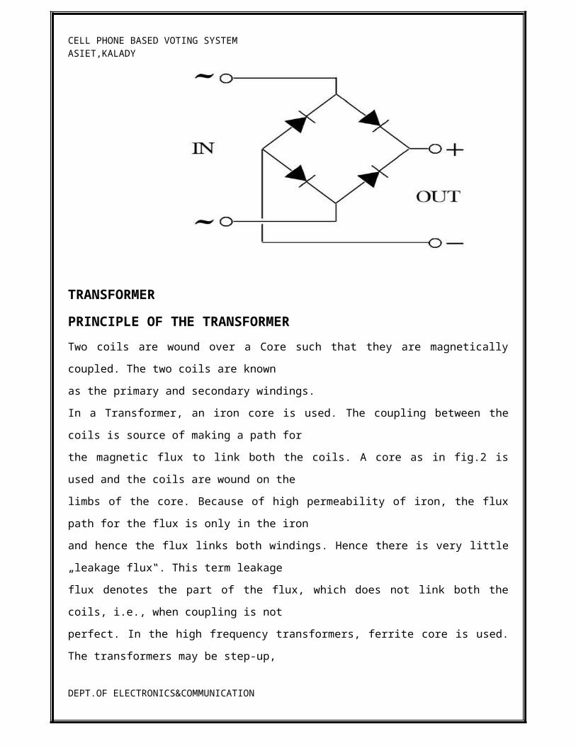
BRIDGE RECTIFIER
A diode bridge is an arrangement of four diodes in a bridge configuration that provides the same
polarity of output for either polarity of input. When used in its most common application, for
conversion of an alternating current (AC) input into direct current a (DC) output, it is known as a
bridge rectifier. A bridge rectifier provides full-wave rectification from a two-wire AC input,
resulting in lower cost and weight as compared to a rectifier with a 3-wire input from a
transformer with a center-tapped secondary winding.[1]
DEPT.OF ELECTRONICS&COMMUNICATION

CELL PHONE BASED VOTING SYSTEM ASIET,KALADY
TRANSFORMER
PRINCIPLE OF THE TRANSFORMER Two coils are wound over a Core such that they are magnetically coupled. The two coils are known
as the primary and secondary windings.
In a Transformer, an iron core is used. The coupling between the coils is source of making a path for
the magnetic flux to link both the coils. A core as in fig.2 is used and the coils are wound on the
limbs of the core. Because of high permeability of iron, the flux path for the flux is only in the iron
and hence the flux links both windings. Hence there is very little „leakage flux‟. This term leakage
flux denotes the part of the flux, which does not link both the coils, i.e., when coupling is not
perfect. In the high frequency transformers, ferrite core is used. The transformers may be step-up,
step-down, frequency matching, sound output, amplifier driver etc. The basic principles of all the
transformers are same.
DEPT.OF ELECTRONICS&COMMUNICATION

CELL PHONE BASED VOTING SYSTEM ASIET,KALADY
4. PCB DESIGN4.1 DESIGN OF PCB1. PRINTED CIRCUIT BOARDS
The miniaturization in electronic equipment design has introduced a new technique known as
PRINTED CIRCUIT BOARD. Printed circuit board is used to interconnect various electronic
circuit printed on it and is provided with holes to accommodate various electronic components.
Printed circuit board (PCB) consists of an insulating base substrate, which is rigid, with metallic
circuitry photo chemically formed up on the substrate. Interconnections between components are
achieved by means of conducting paths (thin Cu film) running on or through the substrate called
tracks. The width of the tracks depends on the amount of current it has to carry. The tracks meet
components to which they are to be connected by means of Land or pads which takes form of
larger area of Cu. The lands may be of different shapes and sizes and have holes drilled through
them. These holes can either accommodate component leads or via-holes. The via -holes also
known as plated through holes (PTH) provide connections through the substrate to other track
areas. These aroused in case of double sided and multilayer PCBs only.
Fig. 4.1 PCB features
Once PCB is designed and fabricated, the circuit can be assembled easily by mounting and
soldering the component in the holes provided for them.
2. ADVANTAGES AND DISADVANTAGES OF USING PRINTED CIRCUIT BOARDS
Advantages
1. Phase saving of wire: In PCB the interconnection between the components is made through
copper tracks instead of using a number of wires carrying electric circuit.
DEPT.OF ELECTRONICS&COMMUNICATION

CELL PHONE BASED VOTING SYSTEM ASIET,KALADY
2. Saving of space: The circuit layout of PCB is designed such that it occupies least space. Also
the use of Cu tracks in place of wires makes the interconnections less bulky. Thus printed circuit
board occupies less space and thus has less weight than the circuit assembled on general-
purpose circuit board.
3. Saving of time: Much time is saved in assembling a circuit over a PCB as compared to
conventional method.
4. Tight connection: As the connections are made automatically through Cu tracks, there is no
chance of loose connection or short circuit
5. Low cost: Mass production can be achieved at lower cost.
6. Reliability: All the above factors bring reliability in performance of the equipment
7. Now-a-days component wiring and assembly can be mechanized by wave soldering of vapour
phase reflow soldering.
Disadvantages
1. As the copper tracks are very thin, they can carry little current. Hence a PCB cannot be used
for circuit with heavy currents because in that case the strips will be heated up and can cause
problems.
2. Soldering needs precautions as the risk of strips being overheated and destroyed is always
there.
3. TYPES OF PCB
There are four types of printed circuit boards
1. Single sided PCB
2. Double sided PCB
3. Multilayered PCB
4. Flexible PCB
1. Single sided PCB: In single sided boards, as the name suggests, copper is coated on one side
of the board or laminate. So the circuitry is only on one side of the board and thus is the simplest
form of PCB. These are simplest to manufacture and hence have least cost of production.
DEPT.OF ELECTRONICS&COMMUNICATION

CELL PHONE BASED VOTING SYSTEM ASIET,KALADY
In these PCB’s, to jump over the Cu tracks jumper wires may be used. Use of jumper is restricted
as far as possible because it decreases the reliability and if their number is more than a few, the
use of double sided PCB should be considered.
Fig.4.3.1 Single sided PCB
2. Double sided PCB: These are used where space is more important than cost of the PCB.
Double sided boards are Cu-coated on both sides. Circuit is etched on both sides but components
are mounted only on one side. Tracks on one side can be joined to tracks on the other side by
means of wire links. Now - a - days, plated through holes (PTH) are available which do the same
thing, but their use makes the PCB expensive. So the total number of PTH should be kept to a
minimum for reasons of economy and reliability.
Fig. 4.3.2 Double sided PCB
3. Multilayered PCB: In multilayered boards, two or more boards with circuitry formed upon
them are carefully aligned, stacked up and bonded together. These boards are used where a very
large circuit has to be fabricated on a single board. At the same time, they are the most complex
from manufacturing point of view. Here also, components are mounted on only one side of the
board. Electrical connections are established from one side of the board to the other and to the
inner layer circuitry by using PTH.
Fig.4.3.3 Multi-layered PCB
DEPT.OF ELECTRONICS&COMMUNICATION

CELL PHONE BASED VOTING SYSTEM ASIET,KALADY
4. Flexible PCB: This is basically a highly flexible variant of the conventional rigid PCB. The
flexible boards are of two types, static and dynamic. Static flexible circuits can be bent into
particular configuration which remains constant throughout product life and results in space
saving. Dynamic flexible circuits can be deformed continuously during operations and are used
to interconnect devices which need to he moved relative to each other.
4. LAMINATES
The board on which the circuit is etched consist of base material\laminate on which conductor
foils are bonded or deposited by some process.
(a) Base material: PCB’s are laminates, i.e., they are made from two or more sheets of base
materials stuck together. There are many materials used for making laminates for PCBs.
Commonly used materials are phenolic resin reinforced with paper filler (phenolic laminates)
for low cost, melamine resin reinforced with glass filler (melamine laminates) for abrasion
resistance, epoxy resin reinforced with glass filler (epoxy laminations ) for higher
mechanical strength, low dimensional change and fungus resistance; Teflon reinforced with
glass (Teflon laminations) for microwave applications; silicon resin reinforced with glass
(silicon laminates) for high temperatures. Reliability of PCB greatly depends on the quality of
base material used.
(b) Conducting material: The conducting materials used for coating the laminate are copper,
silver, gold, brass and aluminum. However, the most widely used material is high purity
electrolytic copper and the laminates coated with copper foil are called as Cu clad laminates.
5. MAKING OF COPPER CLAD LAMINATES The copper clad laminate is manufactured in a heated press which has highly polished
stainless steel press plates.
1. The manufacturing process starts by placing a sheet of copper foil on the lower press plate.
This copper sheet is produced by rolling out a piece of copper or by electroplating.
Electroplating is preferred as it produces more uniform and controllable thickness film.
2. Next the layers of base material are built up on the top of copper foil until required board
thickness is achieved.
3. Once the base material layers have been built up, a final layer is added. For single sided
boards, this final layer is a material, which acts as a release film. And for double-sided
boards, the final layer is a second sheet of copper foil.
DEPT.OF ELECTRONICS&COMMUNICATION

CELL PHONE BASED VOTING SYSTEM ASIET,KALADY
4. Finally, the entire assembly is pressed between the two press plates. The heat treatment of
this assembly bonds the different layers into a complete board i.e., the Cu clad laminate.
Fig. 4.5.1 Making of Cu clad laminate
4.2 PCB DESIGN AND FABRICATION
4.2.1 Design of PCB layout\PatternBefore designing a PCB layout, complete circuit diagram must be available with the designer.
The design of the layout is done on the computer using CAD (Computer Aided Design) or
a standard drawing program. The layout is designed in such a way as to accommodate the
whole circuit in minimum space, avoiding use of jumpers as far as possible. Besides the
complete outlines and interconnections, the layout should include information on:
a. Component hole diameter
b. Conductor width
c. Minimum spacing to be provided between the tracks.
Finally take the print out of the pattern \ layout on a normal A4 size paper. Also make sure that it
is the correct size; Check the layout carefully. This printout is called as positive film.
4.2.2 Film making or Mask makingThe film negative which is finally used as a mask for the direct exposure of the photo resist-
coated PCB is called Film Master. Making of a Negative film (Film master) from a positive
involves the steps listed below. All these steps are preformed in a dark room.
Step 1: Film maker machine: Collect the positive film from the CAD lab. Cut lyth film on which
the negative is to be made to the size equal to the positive film. Start the machine for 5 seconds.
Take the negative film out of the machine by lifting it from the corners.
Step 2: Development: Take a developing tray. Put sufficient developer in the tray so that the
negative film is dipped completely in it. The film should be handled at its corners with the help
of forceps. Now slide the negative film through the developing solution. Turn the tray quickly
DEPT.OF ELECTRONICS&COMMUNICATION

CELL PHONE BASED VOTING SYSTEM ASIET,KALADY
and lift the tray on each side of rotation. This is continued throughout the developing time (1-
1.5min).
Step 3: Stop bath: After the development is over, the film is lifted above the developing tray
(with the help of forceps) for a few seconds so that the excess developer drops out.
Immediately thereafter, the film is immersed in to the stop bath (plain water taken in a tray) for 1
min. This will effectively stop the development action.
Making Negative Film a Positive Film
Step 4: Fixing: Now mix 1 cap of fixer solution in 1 glass of water in a tray. Place the film in
this fixing bath for 0.5 min.
Step 5: Washing: Take out the film from the fixer bath and wash it in running water. Washing is
and important stage in film master preparation because if some chemicals remain on it, they
will decompose and attack the image, causing stained and faced film.
4.2.3 Making of Printed Circuit Boards Various steps involved in the making of PCB are:
1. Preprocessing
2. Photolithography
3. Etching
4. Stripping
5. Tin plating
6. Drilling
7. Testing
8. Loading of components
9. Soldering
DEPT.OF ELECTRONICS&COMMUNICATION

CELL PHONE BASED VOTING SYSTEM ASIET,KALADY
Step 1: Preprocessing:As its name, this step involves all the initial preparation to be made before
actual processing of copper clad laminate starts, such as
a. Collect the printout of the layout from the CAD lab.
b. Cut the copper clad laminate to the required size using a cutter.
c. Clean the board by scrubbing with steel wool or very fine wet sand paper. Dry the
board thoroughly. Make sure that the board is clean and free from fingerprints or any traces of
contamination.
d. Drill tooling\mounting holes.
Step 2: Photolithography: Photolithography is typically the transfer of the copper track and land
pattern from the negative film to a photo sensitive material by selective exposure to a radiation
source such as UV light. It includes the following steps:
a. Pattern transfer:
Apply photo resist. Coat the Cu surface of the Cu clad laminate with a photosensitive material in
a dip coating machine. In lithography, the photosensitive material used is typically a photo resist
(also called resist). Both positive and negative photo resist can be used, but the negative photo
resist which become insoluble on exposure with UV light is almost universally used. Now place
the photo resist- coated board in the oven for 10 minutes to dry the photo resist. Exposure to
UV light: Remove the board from the oven and place it in ultraviolet exposure machine with the
photo resist side facing up. Now place the mask (i.e. the negative film) over the board and
correctly align it with the board’s geometry. Masking tapes can also be used to keep the
negative film in position. Switch on the UV exposure machine for 3 minutes. The UV light falls
on the photo resist only through the lighter or transparent part of the mask. Thus the photo resist
changes its properties only where exposed to radiation. Take out the board from the UV
enclosure by holding it from the edges (using forceps).
b. Development
After exposure, the image of the pattern transferred on the photoresist needs to be developed.
The development stage involves removal of less soluble unexposed area of resist in case of
negative resist and exposed areas in case of positive resist. Here, we are using a negative photo
resist.
DEPT.OF ELECTRONICS&COMMUNICATION

CELL PHONE BASED VOTING SYSTEM ASIET,KALADY
Method: Take a tray and put sufficient developer solution in it such that the board can be
completely dipped in it. Developer solution is prepared by mixing liquid photoresist developer
concentrate with 1 part developer to 9 part of water.
Place the board into the white developer solution. The board should be handled at its corners
with the help of forceps. Now lift the tray on each side in rotation so that the liquid developer is
flowed over and back on the board. This id continued throughout the developing time (1 min).
During development, the developer solution etches away the unexposed region of the negative
photoresist showing copper and the PCB layout will be revealed. After the development is over,
lift the board and wash it in stop bath. This will effectively stop the development action.
c. Fixing
To fix the pattern on the board, mix 1 cap of fixer (blue die solution) in 1 glass of water in tray.
Place the board in the solution for at least 0.5 min. Remove the board from the fixer bath and
wash it under running water.
Photolithography: pattern transfer on negative photo resist
Step 3: Etching
This process is used for removal of PCB’s copper surface, which is not protected by the photo
resist. Thus final Cu pattern is formed on the board after etching.
DEPT.OF ELECTRONICS&COMMUNICATION
CELL PHONE BASED VOTING SYSTEM ASIET,KALADY
The board obtained after photolithography is dipped in an etching solution and gitated for 6-10
min. at 400C. The solution etches \ dissolves away the exposed\ undesired copper areas, leaving
the desired copper pattern on the board. The different
Types of etching solution used are:
a. Ferric Chloride (FeCl3)
b. Chromatic Chloride
c. Cupric Chloride (CuCl2)
d. Alkaline Ammonia
Out of these four, ferric chloride is the most commonly used etchant.
The reaction of FeCl3 and CuCl2 etching solutions with copper are:
FeCl3 + Cu → FeCl2 + CuCl
Ferric chloride Copper Ferrous chloride
CuCl2 + CuCl → 2CuCl
Chromatic acid etching is usually carried out with the addition of Sulphuric acid. Hence it is
called chromic Sulphuric acid. The choice of suitable etchant solution for PCB production
depends on factors like etching speed, copper dissolving capacity, etchant price etc
Step 4: Stripping
After etching, the negative photo resist coating left on the copper pattern can be removed using a
tube of photo resist stripper and the PCB is washed clean under tap water and dried using tissue
paper.
Pattern transfer by etching
DEPT.OF ELECTRONICS&COMMUNICATION
CELL PHONE BASED VOTING SYSTEM ASIET,KALADY
Step 5: Tin Plating (optional)
This is done to provide a fine finish and to protect the copper from oxidation. Also soldering will
appear neater and will flow better. For this, pour a solution made up of fine tin powder mixed
with water into a basin. Place the board in the solution for 10 minutes. The board should then
have a silver finish.
Step 6: Drilling
Drilling is used to create the component lead holes and through holes in a PCB. These holes
pass through the land areas and should be positioned correctly. The drilling process can be
performed by using manually operated drilling machines or by using CNC drilling machines. For
a particular PCB, a wide range of drill holes may be required e.g. smaller holes are required
for component leads whereas larger diameter holes are required for bolting heat sinks, connectors
etc.
Drilling
Step 7: Bare Board Testing
Before mounting the components on the PCB, this bare board needs to ensure that the required
connections exist (i.e. visual inspection), and that there are no short circuit (i.e. continuity
testing) and that drill holes are properly placed. After drilling and testing, the board the board is
now ready to stuff components.
Step 8: Loading Component
Loading of components on a PCB is the process of inserting components in to the holes in the
board. This loading can be done by hand or by machine. Machine is used when there is mass
production of boards of the same pattern.
Step 9: Soldering
Solder the components loaded on the PCB by using either manual soldering or wave soldering
technique. Manual soldering is done with the help of soldering iron, while in wave soldering,
DEPT.OF ELECTRONICS&COMMUNICATION

CELL PHONE BASED VOTING SYSTEM ASIET,KALADY
large number of joints are made simultaneously using a older bath. Wave soldering is a more
efficient method and is used in large scale industry where high productivity is required. During
the soldering process, an external medium is used to increase the flow properties of molten
solder or to improve the degree of wetting. Such a medium is called flux.
Component soldered
7. MANUFACTURING OF SINGLE SIDED PCB’S
From the discussion in section 6.3, the manufacturing of single sided PCB can be illustrated
using this block diagra
DEPT.OF ELECTRONICS&COMMUNICATION
Collect the printout of layout from
CAD lab
Make the negative film(mask) using film makerm/c.
Cut the Cu clad laminate to the size and drill tooling holes
clean the board
Apply photo resist

CELL PHONE BASED VOTING SYSTEM ASIET,KALADY
Block diagram for manufacturing single sided PCB
8. MANUFACTURING OF DOUBLE SIDED PCB Making of double sided PCB is similar to
single sided but require some additional manufacturing processes.Layout design: Unlike the
single sided boards, the double sided boards have layout designs for both side of the board; one
DEPT.OF ELECTRONICS&COMMUNICATION
Expose to UV light through the mask
Develop the image
Etch unwanted copper
Stop resist
Tin plating
Drill holes
Test bare board
Load the components
Solder the components

CELL PHONE BASED VOTING SYSTEM ASIET,KALADY
is called the component side pattern and the other wiring side pattern. While designing on the
computer, first the pattern of the component side and the wiring side is made in one sheet of
the drawing using different colour.Prepare negative film for both side patterns on the separate
lyth film. Cut the double sided board to correct size. Clean the board surfaces and drill the
cooling holes.Apply photoresist coating on both sides of the board and expose them to UV light
through their respective negative film. After developing the image, etching is done to remove the
exposed copper areas. Now the board is placed on CNC machine to drill holes. Unlike single
sided PCBs, doubled sided boards have copper tracks on both sides of the board which need to
be interconnected. Thus additional holes are required along with normal holes for component
insertion. These additional holes are used to connect copper tracks on opposite sides of the board
and are known as via holes. The electrical connection between the two sides of the board is
achieved by plating process. Thus these holes are also referred to as plated through holes
(PTH).The through hole is the way of connecting with the part, which connects the component
side pattern and the wiring side pattern through a thin metallic pipe.
Layout design of a double-sided PCB
Now separate the pattern drawing of the wire side on and the one sheet and the component side
on the other sheet.
DEPT.OF ELECTRONICS&COMMUNICATION

CELL PHONE BASED VOTING SYSTEM ASIET,KALADY
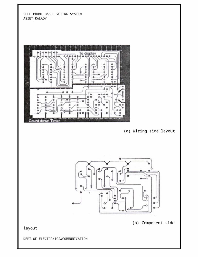
(a) Wiring side layout
(b) Component side layout
DEPT.OF ELECTRONICS&COMMUNICATION

CELL PHONE BASED VOTING SYSTEM ASIET,KALADY
4.3 PCB Layout of cell phone based voting system
DEPT.OF ELECTRONICS&COMMUNICATION

CELL PHONE BASED VOTING SYSTEM ASIET,KALADY
4.3 PCB Component Layout of cell phone based voting system
5. CONCLUSION AND FUTURE ENHANCEMENTS
This report describes the functional and constructional details of Cell phone based voting system
using 16F876A PIC.
DEPT.OF ELECTRONICS&COMMUNICATION

CELL PHONE BASED VOTING SYSTEM ASIET,KALADY
The system can be further modified to enhance its utility. The enhancements are:
Number of candidates could be increased
It can be interfaced with printer to get the hard copy of the result almost instantly from the machine itself.
It can also be interfaced with the personal computer and result can be stored in the central server
Once the result is on the server it could be relayed on the network to various offices of the election conducting authority.thus our project can make results availale at any corner of the world in a matter of seconds.
REFERENCES
[1]. Ramakand Gaykwad, “Op-Amps and Linear Integrated Circuits”,
Prentice Hall India Publishing Company
[2]. Roy Choudhuri, ”Linear Integrated Circuits”,
DEPT.OF ELECTRONICS&COMMUNICATION

CELL PHONE BASED VOTING SYSTEM ASIET,KALADY
New Age International Pvt Ltd
Websites:
1. http://www.housestuffs.com
2. http://www.nationalSemiconductors.com
3. http://www.datasheetcatalog.com
APPENDIX A
#include <16F876A.h>
#device adc=8
#use delay(clock=4000000)
#fuses XT,NOWDT,NOPUT,NODEBUG,NOPROTECT,NOBROWNOUT,NOLVP,NOCPD,NOWRT
#use rs232(baud=9600,parity=N,xmit=PIN_A3,rcv=PIN_A4,bits=8,stream=gsm)
DEPT.OF ELECTRONICS&COMMUNICATION

CELL PHONE BASED VOTING SYSTEM ASIET,KALADY
#define max 4
#include<lcdx.c>
int1 pwd0=0,pwd1=0,pwd2=0,pwd3=0,pwd4=0,pwd5=0,pwd6=0,pwd7=0,flag=0;
int1 blink=0;
int count[4]={0,0,0,0};
#int_TIMER1
TIMER1_isr()
{
blink=~blink;
output_bit(PIN_A1,blink);
}
char timed_getc() {
long timeout;
timeout=0;
while(!kbhit()&&(++timeout<50000)) // 1/2 second
delay_us(10);
if(kbhit()) return(fgetc(gsm));
else return(0);
}
void main()
{
int i;
char c,at[4]="at\r",cmgf[11]="at+cmgf=1\r",cmgr[11]="at+cmgr=1\
r",str[7],cmgd[11]="at+cmgd=1\r";
char upwd[4],pwd[8]
[4]={"111","222","333","444","555","666","777","888"},lcd_data[16],val;
setup_timer_1(T1_INTERNAL|T1_DIV_BY_8);
enable_interrupts(INT_TIMER1);
enable_interrupts(global);
//*pwd$no#
lcd_init();
delay_ms(20);
lcd_putc('\f');
while(1){
up:
lcd_putc('\f');
sprintf(lcd_data,"Name1:%d",count[0]);
DEPT.OF ELECTRONICS&COMMUNICATION

CELL PHONE BASED VOTING SYSTEM ASIET,KALADY
lcd_puts(lcd_data,UL);
sprintf(lcd_data,"Name2:%d",count[1]);
lcd_puts(lcd_data,LL);
sprintf(lcd_data,"Name3:%d",count[2]);
lcd_puts(lcd_data,UR);
sprintf(lcd_data,"Name4:%d",count[3]);
lcd_puts(lcd_data,LR);
for(i=0;i<3;i++) {
fputc(at[i],gsm);
c=timed_getc();
}
for(i=0;i<7;i++)
{
str[i]=timed_getc();
}
for(i=0;i<7;i++)
{
if(str[i]=='E')
goto up;
}
up1:
for(i=0;i<10;i++)
{
fputc(cmgf[i],gsm);
c=timed_getc();
}
for(i=0;i<7;i++)
{
str[i]=timed_getc( );
}
for(i=0;i<7;i++)
{
if(str[i]=='E')
goto up1;
}
for(i=0;i<10;i++)
{
fputc(cmgr[i],gsm);
DEPT.OF ELECTRONICS&COMMUNICATION

CELL PHONE BASED VOTING SYSTEM ASIET,KALADY
c=timed_getc();
}
for(i=0;i<7;i++)
{
str[i]=timed_getc( );
}
for(i=0;i<7;i++)
{
if(str[i]=='E')
goto up;
}
while(timed_getc()!='*');
i=0;
do{
upwd[i]=fgetc(gsm);
}while(upwd[i++]!='$');
upwd[3]='\0';
val=timed_getc();
up3:
for(i=0;i<10;i++)
{
fputc(cmgd[i],gsm);
c=timed_getc();
}
for(i=0;i<7;i++)
{
str[i]=timed_getc( );
}
for(i=0;i<7;i++)
{
if(str[i]=='E')
goto up3;
}
if(strcmp(pwd[0],upwd)==0)
{
if(pwd0==0) pwd0=1;
else continue;
}
DEPT.OF ELECTRONICS&COMMUNICATION

CELL PHONE BASED VOTING SYSTEM ASIET,KALADY
if(strcmp(pwd[1],upwd)==0)
{
if(pwd1==0) pwd1=1;
else continue;
}
if(strcmp(pwd[2],upwd)==0)
{
if(pwd2==0) pwd2=1;
else continue;
}
if(strcmp(pwd[3],upwd)==0)
{
if(pwd3==0) pwd3=1;
else continue;
}
if(strcmp(pwd[4],upwd)==0)
{
if(pwd4==0) pwd4=1;
else continue;
}
if(strcmp(pwd[5],upwd)==0)
{
if(pwd5==0) pwd5=1;
else continue;
}
if(strcmp(pwd[6],upwd)==0)
{
if(pwd6==0) pwd6=1;
else continue;
}
if(strcmp(pwd[7],upwd)==0)
{
if(pwd7==0) pwd7=1;
else continue;
}
switch(val){
case '1':count[0]=count[0]+1;
break;
DEPT.OF ELECTRONICS&COMMUNICATION

CELL PHONE BASED VOTING SYSTEM ASIET,KALADY
case '2':count[1]=count[1]+1;
break;
case '3':count[2]=count[2]+1;
break;
case '4':count[3]=count[3]+1;
break;
}
}}
APPENDIX B
COST ANALYSIS OF COMPONENTS USED
Sr. no Equipment Quantity Rate (in Rs.)
1 PIC 16F73 1 120 2 Voltage Regulator
7805 1 20
3 2 line LCD display 1 140 4 Transformer 1 60 5 Crystal Oscillator 2 10 6 Switch 5 10 7 LED 3 6
DEPT.OF ELECTRONICS&COMMUNICATION

CELL PHONE BASED VOTING SYSTEM ASIET,KALADY
8 Resistors(1KΩ,10KΩ)
4 3
9 Capacitors(22pf,.1μf,10μf,470μf,1000μf)
8 10
10 Diodes 4 8 11 D9 connecter 1 1512 Sip resistor 1 713 Berge strip 1 314 IC base 2 30
Total 442
APPENDIX C
PIC MICROCONTROLLER DATA SHEETS
DEPT.OF ELECTRONICS&COMMUNICATION

CELL PHONE BASED VOTING SYSTEM ASIET,KALADY
DEPT.OF ELECTRONICS&COMMUNICATION

CELL PHONE BASED VOTING SYSTEM ASIET,KALADY
DEPT.OF ELECTRONICS&COMMUNICATION

CELL PHONE BASED VOTING SYSTEM ASIET,KALADY
DEPT.OF ELECTRONICS&COMMUNICATION

CELL PHONE BASED VOTING SYSTEM ASIET,KALADY
DEPT.OF ELECTRONICS&COMMUNICATION

CELL PHONE BASED VOTING SYSTEM ASIET,KALADY
DEPT.OF ELECTRONICS&COMMUNICATION
CELL PHONE BASED VOTING SYSTEM ASIET,KALADY
DEPT.OF ELECTRONICS&COMMUNICATION

CELL PHONE BASED VOTING SYSTEM ASIET,KALADY
DEPT.OF ELECTRONICS&COMMUNICATION

CELL PHONE BASED VOTING SYSTEM ASIET,KALADY
DEPT.OF ELECTRONICS&COMMUNICATION