Embed Size (px)
Citation preview
WARSAW UNIVERSITY OF TECHNOLOGY
Faculty of Electronics
and Information Technology
Ph.D THESIS
Bartłomiej Salski, M.Sc.
Application of semi-analytical algorithms
in the finite-difference time-domain modeling
of electromagnetic radiation and scattering problems
Supervisor
Professor Wojciech Gwarek, Ph.D., D.Sc.
Warsaw, 2010

2

3
Abstract
This dissertation is focused on the semi-analytical finite-difference time-domain (FDTD)
modeling of electromagnetic radiation and scattering problems. A combination of analytical
and numerical methods may lead to decreased computational effort at no cost to the accuracy
of the obtained results.
Chapter 3 deals with electromagnetic modeling of periodic structures using the FDTD method
supplemented with periodic boundary conditions, derived from the analytical Floquet
theorem. A developed algorithm is then applied to the analysis of one-, two-, and three-
dimensional eigenvalue problems of periodic structures. As an extension of the algorithm’s
applicability to deterministic problems, methods and computational models for the analysis of
a diffraction of plane wave obliquely incident on periodic structure are introduced and
investigated. For the purpose of final evaluation of the introduced methods, models with a
Gaussian beam incident on a periodic structure are introduced and validated.
Chapter 4 of this dissertation depicts the author’s consideration on the possibility of applying
the FDTD method to the modeling of imaging phenomenon, which is widely used in optical
microscopes. A coupling of the FDTD method with the algorithms based on approximate
methods dedicated to optical diffraction modeling is introduced and validated. The elaborated
method leads to increased accuracy of the overall modeling of an optical path in modern
microscopes.
Chapter 5 is focused on the transformation of electromagnetic fields in a near zone of
axisymmetrical structures. The method introduced and derived by the author of this
dissertation enables a significant reduction in computational effort of the already existing
FDTD schemes for axisymmetrical problems which have no common symmetry axis for all
the consituent elements, such as off-axis feeded Cassegrain antenna.

4
Streszczenie
Praca poświęcona jest częściowo analitycznemu modelowaniu elektromagnetycznemu
zagadnień promieniowania oraz dyfrakcji fali elektromagnetycznej metodą różnic
skończonych w dziedzinie czasu (ang. finite-difference time-domain). Kombinacja metod
analitycznych z metodami numerycznymi może prowadzić do zmniejszenia nakładów
obliczeniowych bez dodatkowych kosztów w postaci zmniejszonej dokładności
otrzymywanych wyników obliczeń.
Rozdział 3 rozprawy dotyczy modelowania elektromagnetycznego struktur periodycznych
metodą różnic skończonych w dziedzinie czasu, uzupełnioną o periodyczne warunki
brzegowe wyprowadzone z analitycznego twierdzenia Floquet'a. Algorytm ten zastosowany
jest następnie do analizy problemów własnych jedno-, dwu- oraz trójwymiarowych struktur
periodycznych. W ramach problemów deterministycznych, wprowadzone i opisane są także
metody i modele obliczeniowe dyfrakcji fali płaskiej padającej pod dowolnym kątem na
strukturę periodyczną. W celu weryfikacji opisanych dotychczas metod, wprowadzone zostają
modele do obliczeń padania fali elektromagnetycznej o przestrzennym rozkładzie Gaussa na
strukturę periodyczną.
Rozdział 4 rozprawy przedstawia rozważania autora na temat możliwości zastosowania
metody różnic skończonych w dziedzinie czasu do modelowania zjawiska obrazowania,
szeroko stosowanego w mikroskopach optycznych. Zaproponowana i zweryfikowana została
możliwość sprzężenia metody różnic skończonych w dziedzinie czasu z algorytmem opartym
na aproksymacyjnych metodach modelowania dyfrakcji optycznej. Opracowana metoda
pozwala na zwiększenie dokładności modelowania toru optycznego we współczesnych
mikroskopach.
Rozdział 5 poświęcony jest przekształceniu pola elektromagnetycznego w strefie bliskiej dla
problemów osiowosymetrycznych. Metoda - wyprowadzona i zweryfikowana przez autora
pracy - pozwala na znaczne zwiększenie efektywności obliczeń elektromagnetycznych
struktur osiowosymetrycznych, takich jak antena typu Cassegrain, której poszczególne
elementy nie posiadają wspólnej osi symetrii.

5
Acknowledgments
I would like to express my sincere gratitude and appreciation to Professor Wojciech Gwarek
for his continuing support and valuable advice during these over four years of my studies
toward this dissertation. It has been an excellent opportunity for me to gain experience in
computational electromagnetics, which I will always be grateful for.
This dissertation would not come into existence without the advisory role of Dr. Malgorzata
Celuch, and numerous scientific conversations we had throughout my research studies. I
really appreciate this support and wish to thank for all the fruitful comments.

6
Contents
Abstract ..................................................................................................................................3 Streszczenie ............................................................................................................................4 Acknowledgments ..................................................................................................................5 Contents .................................................................................................................................6 List of Figures ........................................................................................................................8 List of Tables ....................................................................................................................... 11 List of Publications ............................................................................................................... 12 Symbols ............................................................................................................................... 14 Acronyms and abbreviations ................................................................................................. 15 Introduction .......................................................................................................................... 17
1.1 Motivation and Objectives .................................................................................... 17 1.2 Thesis Overview ................................................................................................... 18 1.3 Original Contribution ............................................................................................ 19
Finite-Difference Time-Domain –......................................................................................... 21 Overview of the Method ....................................................................................................... 21
2.1 Principles of the Method ....................................................................................... 21 2.2 Advantages and Limitations .................................................................................. 27
FDTD Modeling of Electromagnetic Diffraction from Periodic Structures ............................ 30 3.1 Introduction .......................................................................................................... 30 3.2 State-of-the-art in FDTD Modeling of Periodic Structures ..................................... 31 3.3 Periodic Boundary Conditions ............................................................................... 35 3.4 Eigenvalue Periodic Problems ............................................................................... 39
3.4.1 3D Eigenvalue Periodic Problems ........................................................................ 40 3.4.2 V2D Eigenvalue Periodic Problems ..................................................................... 48
3.5 FDTD Modeling of Scattering from Periodic Structures ........................................ 52 3.5.1 Plane Wave Illumination of Periodic Structures.................................................... 55
3.5.1.1 Plane Wave Source over Infinitely Periodic Structure .................................... 55 3.5.1.2 Waveguide Mode over Infinitely Periodic Structure ...................................... 71
3.5.2 Gaussian Beam Illumination of Periodic Structures .............................................. 85 3.6 Summary............................................................................................................... 91
Hybrid FDTD Modeling ....................................................................................................... 92 of the Far-Field Microscopy Imaging .................................................................................... 92
4.1 Introduction .......................................................................................................... 92 4.2 Theoretical Background ........................................................................................ 94 4.3 State-of-the-art ...................................................................................................... 98 4.4 Hybrid FDTD Modeling of the Wide-Field Microscopy ........................................ 99
4.4.3 Introduction to Wide-Field Microscopy ................................................................ 99 4.4.4 Hybrid FDTD-Fresnel Modeling of the Wide-Field Microscope ......................... 101 4.4.5 Computational Tests........................................................................................... 104
4.5 Hybrid FDTD Modeling of the Confocal Microscopy ......................................... 112 4.5.1 Introduction to the Confocal Microscopy ........................................................... 112 4.5.2 Hybrid FDTD-Fresnel Modeling of the Confocal Microscope ............................ 116 4.5.3 Computational Tests........................................................................................... 116
4.6 Summary............................................................................................................. 118 Near-to-Near Transformation in Axisymmetrical Structures ............................................... 119
5.1 Introduction ........................................................................................................ 119 5.2 Basic Concept ..................................................................................................... 120

7
5.3 Theoretical Background ...................................................................................... 123 5.4 Radial Current Component .................................................................................. 126 5.5 Transverse Current Component ........................................................................... 128 5.6 Benchmark Tests ................................................................................................. 131 5.7 Summary............................................................................................................. 134
Conclusions and perspectives ............................................................................................. 135 Periodic Boundary Conditions ............................................................................................ 138 Brillouin zone ..................................................................................................................... 143 Spherical coordinate system ............................................................................................... 147 Cylindrical coordinate system ............................................................................................. 149 Lens imaging algorithm ...................................................................................................... 151 Bibliography....................................................................................................................... 155

8
List of Figures
Fig.2.1. Yee cell. .................................................................................................................. 23 Fig.3.1. Periodic boundary conditions along the z-axis in the CL-FDTD algorithm. .............. 36 Fig.3.2. Periodic boundary conditions along the x-axis in the CL-FDTD algorithm. .............. 37 Fig.3.3. Periodic boundary conditions in the xy-plane in the CL-FDTD algorithm. ............... 38 Fig.3.4. Spectrum of the current injected into an empty air cube ........................................... 41 (ψx = 0 rad, 50mm x 20mm x 10mm).................................................................................... 41 Fig.3.5. Distribution of Ez (left) and Hx (right) components in the xy-plane ........................... 41 of the real FDTD grid at f = 7.49GHz (ψx = 0 rad, 50mm x 20mm x 10mm). ........................ 41 Fig.3.6. Distribution of Ez (left), Hx (right) and Hy (bottom) components in the xy-plane ....... 42 of the real FDTD grid at f = 9.6GHz (ψx = 0 rad, 50mm x 20mm x 10mm). .......................... 42 Fig.3.7. Rectangular lattice of GaAs rods (left) and its CL-FDTD model (right). .................. 43 Fig.3.8. Envelope of electric (left) and magnetic (right) field components ............................ 43 on the real FDTD grid at f = 23.08 THz (ψx = ψy = π/2 rad). ................................................. 43 Fig.3.9. PBG diagram (left) in the first irreducible Brillouin zone (right) .............................. 44 of the PhC lattice shown in Fig.3.7. ...................................................................................... 44 Fig.3.10. Photonic crystal lattice (a = 1µm) made of silica balls (εr = 2.25, r = 0.15µm) located in a vacuum. 45 Fig.3.11. Electric (left) and magnetic (right) field components in the xy-plane at f = 590 THz. ............................................................................................................................................. 45 Fig.3.12. Electric (left) and magnetic (right) field components in the xz-plane at f = 590 THz. ............................................................................................................................................. 46 Fig.3.13. Single cell of the rectangular body centered cubic lattice (εr = 25, a = 0.6µm). ....... 46 Fig.3.14. PBG diagram (left) in the first irreducible Brillouin zone (right) ............................ 47 of the body centered cubic lattice shown in Fig.3.13. ............................................................ 47 Fig.3.15. Spectrum of the electric current injected into a rectangular air-box ........................ 49 (ψx = 0 rad, βf = 0 rad/mm). .................................................................................................. 49 Fig.3.16. Snapshots of the electric Ey (left column) and magnetic Hz (right column) components at both f1 = 13.62GHz (top row) and f2 = 27.18GHz (bottom row) modes indicated in Fig.3.15. ............................................................................................................ 50 Fig.3.17. Spectrum of the electric current injected into a rectangular air-box ........................ 51 (ψx = 7.9807 rad, βf = 0.20944 rad/mm). ............................................................................... 51 Fig.3.18. Snapshot of the electric component Ey at f1 = 19.98GHz ........................................ 52 for the mode indicated in Fig.3.17. ....................................................................................... 52 Fig.3.19. TE (left) and TM (right) polarization of an incident wave. ..................................... 54 Fig.3.20. Oblique incidence of a plane wave in the xy-plane ................................................. 56 on the structure periodic along the x-axis. ............................................................................. 56 Fig.3.21. FDTD model for an oblique plane wave incidence ................................................. 57 on the structure periodic along the x-axis. ............................................................................. 57 Fig.3.22. Plane wave illumination at the real (left) and imaginary (right) FDTD grids at f = 10GHz, incident at αinc = 300, snapped at the same time instant. 58 Fig.3.23. Scattering pattern shown in a logarithmic scale for the plane wave ........................ 61 incident at αinc = 300 (φinc = 3000) in an empty air region (f = 10GHz, L = 40mm)................. 61 Fig.3.24. Scattering patterns for the plane wave incident at αinc = 300 in an empty air region 61 with a varying length L (f = 10GHz, L = N*40mm)............................................................... 61 Fig.3.25. Dielectric coated PEC cross-shaped grating (d = 100 mm, ε1 = 2.56 ε0). ................ 62 Fig.3.26. Specular power reflection from the dielectric-coated PEC cross-shaped grating ..... 63

9
(d = 100 mm, αinc = 300) compared with the FETD method. ................................................. 63 Fig.3.27. Angular scattering pattern in power scaling............................................................ 64 for the dielectric-coated PEC cross-shaped grating (d = 100 mm, αinc = 300, f = 1.2GHz) ..... 64 obtained in one (red) and ten (blue) periods model................................................................ 64 Fig.3.28. Specular reflection (blue curve), as shown in Fig.3.26, compared with a wideband data collection (red curve) matched only at a single frequency marked with dots. ................. 66 Figures in the right column show relative discrepancy between both curves in the left column. ............................................................................................................................................. 66 Fig.3.29. Cross-section view of a poly-to-active stack........................................................... 67 Fig.3.30. Reflection coefficient for a TE polarized illumination incident at 250 ..................... 68 on the target shown in Fig.3.29. ............................................................................................ 68 Fig.3.31. Angular scattering patterns (normalized power scaling) calculated in an incident plane for the infinite array of 10mm x 10mm metal patches modeled with ............................ 70 1x1 (red) and 2x2 (blue) matrix of patches. ........................................................................... 70 Fig.3.32. Plane wave representation of waveguide mode propagation. .................................. 72 Fig.3.33. Waveguide model with PBC for the scattering of periodic structures. .................... 73 Fig.3.34. Reflection coefficient |S11| obtained in a periodic empty model .............................. 75 excited with a TE mode template (L=10mm, fc=7.5GHz, f=15GHz, εeff=0.75). ...................... 75 Fig.3.35. FDTD model of a dielectric grating........................................................................ 76 Fig.3.36. Reflection coefficient |S11| obtained for a dielectric grating (εr=2.2) ....................... 77 excited with a TE mode template (L=10mm, fc=7.5GHz, f=15GHz, εeff=0.75). ...................... 77 Fig.3.37. Normalized scattering pattern for the dielectric grating shown in Fig.3.35 illuminated with a TE polarized plane wave at αinc = 300 (f = 15GHz). ................................. 77 Fig.3.38. Reflection coefficient |S11| obtained for a dielectric grating (εr=2.2) ....................... 78 excited with a TM mode template (L=10mm, fc=7.5GHz, f=15GHz, εeff=0.75)...................... 78 Fig.3.39. Normalized angular scattering pattern for the dielectric grating shown in Fig.3.35 illuminated with a TM polarized plane wave at αinc = 300 (f = 15GHz). ................................ 78 Fig.3.40. Waveguide model with PEC sides for the scattering of periodic structures. ............ 80 Fig.3.41. Precision magnitude of an incidence angle versus the length of the model ............. 81 of the dielectric coated PEC cross-shaped grating (d = 100 mm, λ = 800mm, αinc = 300). ..... 81 Fig.3.42. Reflection coefficient versus the length of the model of the dielectric coated ......... 81 PEC cross-shaped grating (d = 100 mm, λ = 800mm, αinc = 300). ......................................... 81 Fig.3.43. Angular scattering pattern (power scaling) for the dielectric coated ........................ 83 PEC cross-shaped grating (d = 100 mm, αinc = 300, f = 2.65GHz) obtained in a 17 periods model. .................................................................................................................................. 83 a) b) ............................................................................................................................ 84 Fig.3.44. Waveguide model with PEC sidewalls for the infinite spot size scattering.............. 84 of infinite (a) / finite (b) periodic structure. ........................................................................... 84 Fig.3.45. Shape of a Gaussian beam in a focal plane (y = 0). ................................................. 86 Fig.3.46. Scheme of the FDTD model for a Gaussian beam obliquely incident ..................... 87 on the structure periodic along the x-axis. ............................................................................. 87 Fig.3.47. Snapshots of the electric field (left) and the envelope (right) for a TE polarized ..... 88 2D Gaussian beam incident in the xy-plane (λ = 0.5µm, w0 = 1µm, AOI = 250). ................... 88 Fig.3.48. Reflection coefficient for a TE polarized 2D Gaussian beam .................................. 89 incident at 250 on the target shown in Fig.3.29. ..................................................................... 89 Fig.3.49. Absolute deviation of Rss with a diminishing spot size ........................................... 90 for the poly-to-active stack (pitch = 320nm). ........................................................................ 90 Fig.3.50. Absolute deviation of Rpp with a diminishing spot size........................................... 90 for the poly-to-active stack (pitch = 320nm). ........................................................................ 90

10
Fig.4.1. Point source radiation through the aperture. ............................................................. 94 Fig.4.2. Single lens imaging scenario. ................................................................................. 100 Fig.4.3. FDTD model of EM wave scattering from a target. ................................................ 102 Fig.4.4. Axial distribution of the point spread function. ...................................................... 105 Fig.4.5. Lateral distribution of the point spread function. .................................................... 105 Fig.4.6. Computation time of the point spread function versus NA. .................................... 107 Fig.4.7. Angular scattering pattern of the PEC plate (w=16µm) illuminated at λ=500nm. ... 108 Fig.4.8. Image of the isolated PEC plate (w=16µm) at yi = 60mm (intensity scaling). ......... 109 Fig.4.9. Images of two isolated PEC plates (w=8µm) at yi = 60mm..................................... 110 separated by a variable distance (t = 4, 8, 12, 16 µm). ......................................................... 110 Fig.4.10. Normalized spectrum of the illumination plane wave (power scaling). ................. 111 Fig.4.11. Image of the isolated PEC plate (w=16µm) at yi = 60mm (λ = 450:50:750nm). .... 111 Fig.4.12. Scenario of confocal scanning microscope ........................................................... 113 (illumination mode – left, scanning mode - right). .............................................................. 113 Fig.4.13. Divergence angle θ of a Gaussian beam. .............................................................. 114 Fig.4.14. Point spread function of the detection path. .......................................................... 117 Fig.4.15. Image of the trench (left) and the line (right) with the green dotted line ............... 118 depicting the real shape of the target. .................................................................................. 118 Fig.5.1. NTF surface surrounding V2D BOR FDTD model of axisymmetrical antenna....... 121 Fig.5.2. Current loop antenna. ............................................................................................. 123 Fig.5.3. Magnitude of magnetic field |Hφ| as a function of relative distance r from the loop center (see Eq.5.38). ........................................................................................................... 131 Fig.5.4. Accuracy histogram for points shown in Fig.5.3 .................................................... 132 for consecutive number of terms M in Eq.5.38. ................................................................... 132 Fig.5.5. Comparison between Eq.5.38 and corresponding NTF solution.............................. 134 Fig.A2.1. Square lattice (a) and the corresponding reciprocal lattice (b) with the irreducible Brillouin zone (c)................................................................................................................ 144 Fig.A2.2. Hexagonal lattice (a) and the corresponding reciprocal lattice (b) with the irreducible Brillouin zone (c). ............................................................................................. 145 Fig.A2.3. Body centered cubic lattice (a) and the corresponding reciprocal face centered (fcc) lattice (b). ........................................................................................................................... 146 Fig.A3.1. Spherical coordinate system view. ...................................................................... 147 Fig.A4.1. Cylindrical coordinate system view. .................................................................... 149

11
List of Tables
Table 3.1. Maximum electric field intensities of the incident beams shown in Fig.3.24. ........ 62 Table 3.2. Values taken from the angular scattering pattern shown in Fig.3.27. ..................... 64 Table 3.3. Values taken from the angular scattering patterns shown in Fig.3.31. ................... 71 Table 3.4. Values taken from the reflection coefficient shown in Fig.3.34............................. 75 Table 3.5. Values taken from the angular scattering patterns shown in Fig.3.43. ................... 83 Table 3.6. Pros and cons of the methods introduced in Section 3.5.1. .................................... 85 Table 4.1. Resolution of the images shown in Fig.4.5 ......................................................... 106 compared with theoretical estimations. ............................................................................... 106 Table 4.2. Magnification of the obtained images as shown in Fig.4.9. ................................. 110 Table 5.1. Speedup factor for all of EM field components .................................................. 133 obtained from the contribution of Iz(φ’) and Iρ(φ’). ............................................................. 133

12
List of Publications
Magazines
[1]. B.Salski, W.K.Gwarek, "Near-to-Near Transformation in axisymmetrical antenna
problems", IEEE Trans. Antenna Propagat., vol.55, No.8, Aug.2007, pp.2157-2162.
[2]. B. Salski, W. Gwarek, M. Celuch, ”Electromagnetic FDTD modeling of optical
problems,” Elektronika – konstrukcje, technologie, zastosowania, no. 4, pp. 53-55,
2009.
[3]. B. Salski and W. K. Gwarek, "Hybrid finite-difference time-domain Fresnel modeling
of microscopy imaging", Applied Optics, vol. 48, issue 11, pp. 2133-2138, 2009.
[4]. B. Salski, M. Celuch, W. Gwarek, ”FDTD for nanoscale and optical problems,”
Microwave Magazine, accepted for publication, April, 2010.
Conferences
[1]. J.Antoniuk, B.Salski, W.K.Gwarek, "Slotted waveguide as excitation systems of
microwave ovens", 12th Conf. on Microwave Technique COMITE-2003, Pardubice,
the Czech Republic, Sept.2003, pp.85-88.
[2]. P.Kopyt, B.Salski, W.K.Gwarek, "Resonator-based method for estimation of complex
permittivity of materials", 12th Conf. on Microwave Technique COMITE-2003,
Pardubice, the Czech Republic, Sept.2003, pp.117-120.
[3]. B.Salski, M.Celuch, W.K.Gwarek, "Evaluation of FDTD regimes for scattering from
periodic structures", 23rd Annual Review of Progress in Applied Computational
Electromagnetics, Verona, March 2007, pp.1815-1822.
[4]. B.Salski, W.K.Gwarek, M.Celuch, "Comparison of FDTD excitation models for
scatterometry of periodic reticles", 2007 IEEE AP-S Intl.Symp., Honolulu, June 2007,
pp. 1673-1676.
[5]. B.Salski, M.Celuch, W.Gwarek, "Enhancements to FDTD modeling for optical
metrology applications", SPIE Optical metrology - 18th Intl. Congress on Photonics in
Europe, Munich, June 2007.
13
[6]. D.Kandel, M.Adel, B.Dinu, B.Golovanevsky, P.Izikson, V.Levinski, I.Vakshtein,
P.Leray, M.Vasconi, B.Salski, "Differential signal scatterometry overlay metrology:
an accuracy investigation", Optical Measurement Systems for Industrial Inspection V,
Proceedings of SPIE, vol. 6616, 2007.
[7]. B.Salski, M.Celuch, W.K. Gwarek, "Review of Complex Looped FDTD and its new
applications", 24th Annual Review of Progress in Applied Computational
Electromagnetics, Niagara Falls, March - April 2008.
[8]. P. Leray, S. Cheng, D. Kandel, M. Adel, A. Marchelli, I. Vakshtein, M. Vasconi and
B. Salski, "Diffraction based overlay metrology: accuracy and performance on front
end stack", Metrology, Inspection, and Process Control for Microlithography XXII,
Proceedings of SPIE, vol. 6922, 2008.
[9]. B. Salski, M. Celuch, W. Gwarek, "FDTD modelling of finite spot scatterometry",
17th International Conference on Microwaves, Radar and Wireless Communications:
MIKON 2008, Wroclaw, May 2008.
[10]. B. Salski and W. K. Gwarek, "Hybrid FDTD-Fresnel Modeling of Microscope
Imaging", to be presented at the International Conference on Recent Advances in
Microwave Theory and Applications MICROWAVE-08 in Jaipur, Rajastan, India,
November 21-24, 2008.
[11]. B. Salski and W. K. Gwarek, "Hybrid FDTD-Fresnel modeling of the scanning
confocal microscopy", Proceedings of SPIE Scanning Microscopy 2009, vol. 7378,
2009.
[12]. P. Leray, S. Cheng, D. Laidler, D. Kandel, M. Adel, B. Dinu, M. Polli, M. Vasconi, B.
Salski, “Overlay metrology for double patterning processes,” Metrology, Inspection,
and Process Control for Microlithography XXIII, Proceedings of SPIE, vol. 7272,
2009.
[13]. B. Salski, M. Celuch, W. Gwarek, ”Electromagnetic simulations of periodic structures
with FDTD tools,” Progress in Electromagnetic Research Symposium, Moscow, Aug.
2009.

14
Symbols
E electric field
H magnetic field
D electric flux denisty
B magnetic flux density
J electric current density
ε0 free-space permittivity
µ0 free-space permeability
ρ electric charge density
c electromagnetic wave velocity in a free-space
I electric current
K magnetic current
A vector potential
γ propagation constant
α attenuation constant
β phase constant
βf longitudinal phase constant
η intrinsic impedance of vacuum
k propagation vector
ψ Floquet phase shift per period
λ wavelength
f frequency
εeff effective permittivity
w0 Gaussian beam spot radius
j square root of –1 (notation common in electronics)
i square root of –1 (notation common in physics)
ℑ Fourier transform

15
Acronyms and abbreviations
CAD computer aided design
R&D research and development
EM electromagnetic
FDTD finite-difference time-domain
FEM finite element method
MoM method of moments
CL-FDTD complex-looped FDTD
NTN near-to-near
PBC perodic boundary conditions
1D one-dimensional
2D two-dimensional
3D three-dimensional
V2D vector 2D
ABC absorbing boundary
PML perfectly matching layer
TEM transverse electromagnetic
TF total field
SF scattered field
NTF near to far
BOR body of revolution
TE transverse electric
TM transverse magnetic
ASM array scanning method
PEC perfect electric conductor
PMC perfect magnetic conductor
PBG photonic bandgap
GaAs Gallium Arsenide
IC integrated circuit
LSI large scale integration
FSS frequency selective structure
FETD FEM time domain

16
RCWA rigorous coupled wave analysis
AOI angle of incidence
PLW plane wave
DFT direct Fourier transform
FFT fast Fourier transform
ASP angular scattering pattern
SNR signal to noise ratio
CD critical dimension
GBW Gaussian beam wall
NA numerical aperture
PSF point spread function
FWHM full width at half maximum
DOF depth of field
bcc body centered cubic
fcc face centered cubic
WG waveguide

17
Chapter 1
Introduction
1.1 Motivation and Objectives
During the last several years computer aided design (CAD) has become an essential tool in
the engineering practice as well as in the research and development (R&D) activities. It is
hard to imagine a professional design work without specialized software applications
supported with modern computing units. It is mainly an outcome of dynamic growth that can
be observed in many branches of science, but also a result of an increasing complexity of
modern devices. Old-fashioned cut-and-try techniques were found highly ineffective, so in the
recent years a lot of effort has been focused on the development of numerical methods and
algorithms to apply in various scientific disciplines.
The subject of this thesis concerns CAD modeling of electromagnetic (EM) phenomena. In
particular, the dissertation is focused on one of the most recognized numerical methods
in electromagnetics, namely the finite-difference time-domain (FDTD) method,
originally introduced in electromagnetics by Kane Yee in 1966. Some details about the FDTD
method will be recalled in Chapter 2. It should be emphasized, however, that an increasing
confidence in EM modeling stimulates growing market requirements, which are often
beyond computational capabilities of the state-of-the-art computer platforms. In consequence,
a lot of effort is continuously undertaken by many scientists to solve or at least alleviate
that mismatch. One of the possible solutions to the huge demand of computational speed
and effectiveness lies in investing in more powerful processing units. On the other hand,
there can be observed an increasing popularity of hybrid EM modeling, which combines
different modeling methods, enabling a reduction in computational effort for specific
EM problems. Some of these approaches may be called partially analytical, in reference
to the algorithms that combine classical numerical methods, like FDTD, FEM, MoM, etc.,
with analytical formulae. This dissertation addresses some of partially analytical methods
coupled with the FDTD method.

18
The motivation of this thesis follows from the demand to extend the applicability of the
FDTD method to the analysis of radiation and scattering problems, which were formerly
highly ineffective, or even impossible to handle without deterioration of accuracy. The
following thesis is posed and will be proven:
The partially analytical FDTD methods can substantially speed up the
computation of electromagnetic radiation and scattering problems without
deterioration of accuracy.
In this dissertation, three auxiliary statements will also be addressed and confirmed:
1. Electromagnetic modeling of plane wave scattering from periodic
structures can be made computationally more effective by applying FDTD
with Floquet theorem (CL-FDTD) and a number of specialized models for
excitation and parameter extraction.
2. Approximate optical modeling of lens imaging systems based on a Fresnel
diffraction theory can be successfully supported with the rigorous FDTD
modeling, improving modeling accuracy.
3. The alternative partially analytical method of near-to-near field
transformation for axisymmetrical problems, requiring less
computational efforts than the direct integration technique, can be
developed.
The study presented in this dissertation extends computational capabilities of the FDTD
method for new domains of problems, introducing simplified computational models based on
analytical transformations or approximate assumptions.
1.2 Thesis Overview
Chapter 2 presents a brief outline of the FDTD method, emphasizing its major advantages
over the other modeling methods, but also pointing out its inherent limitations.
19
Chapter 3 covers the issue of the FDTD modeling of periodic structures. Implementation of
1D, 2D and 3D periodic boundary conditions (PBC) is presented and its applicability for
analysis of eigen-problems is studied. Next, modeling of a plane wave scattering from
periodic structures using the FDTD algorithm with PBC is investigated. A near-to-far
transformation is adapted in the periodic FDTD algorithm to extract a radiation/scattering
pattern of an infinite periodic problem in a finite FDTD model. Extended studies of selective
frequency properties of PBC are covered. A waveguide model in the classic FDTD algorithm
is also studied as an alternative for the periodic FDTD algorithm to the analysis of plane wave
scattering from periodic structures. Finally, a Gaussian beam illumination of an infinite
periodic structure is discussed to show the prospective limitations of the periodic FDTD
approach.
Chapter 4 presents original study by the author of this thesis on the applicability of the FDTD
method to modeling of an imaging phenomenon, which plays an important role in optical
microscopes when a target's size becomes comparable to operating wavelengths. The issue of
the potential application of the FDTD method coupled with a particular approximate optical
approach to enhance capabilities of the overall algorithm of the far-field microscope imaging
is then addressed.
Chapter 5 is focused on the near-to-near (NTN) transformation technique for the
axisymmetrical problems, originally developed by the author of this thesis.
1.3 Original Contribution
This thesis presents the author’s original contribution in the following areas:
- development, implementation and evaluation of 2D and 3D periodic boundary
conditions in 3D CL-FDTD algorithm (Chapter 3);
- development, implementation and evaluation of 1D and 2D periodic boundary
conditions in V2D CL-FDTD algorithm (Chapter 3);
- development, implementation and evaluation of plane wave source in a 3D CL-
FDTD algorithm (Chapter 3);
- development, implementation and evaluation of near-to-far transformation in a 3D
CL-FDTD algorithm (Chapter 3);

20
- investigation of practical frequency bandwidth of the CL-FDTD algorithm (Chapter
3);
- evaluation of a waveguide model for plane wave scattering from periodic structures
in the classic FDTD algorithm (Chapter 3);
- development, implementation and evaluation of V2DS CL-FDTD algorithm
(Chapter 3);
- development, implementation and evaluation of a waveguide model of the plane
wave scattering from periodic structures in CL-FDTD algorithm (Chapter 3);
- simulations of a Gaussian beam illumination of an infinite periodic structure
(Chapter 3);
- development, implementation and evaluation of a hybrid FDTD-Fresnel algorithm
applicable to the modeling of wide-field microscope tools (Chapter 4);
- development, implementation and evaluation of a hybrid FDTD-Fresnel algorithm
applicable to the modeling of confocal microscope tools (Chapter 4);
- derivation, development and evaluation of near-to-near transformation for
axisymmetrical structures (Chapter 5).

21
Chapter 2
Finite-Difference Time-Domain – Overview of the Method
2.1 Principles of the Method
Electromagnetism is a notion that bonds time-varying electric and magnetic fields together
into inseparable quantities. Yet, up to the middle of the 19th century, scientists recognized
both electric and magnetic fields as independent of each other. Afterwards, at the time when
electricity and magnetism started to be extensively studied, Ampere’s and Faraday’s laws
were the first that strictly related the motion of both physical quantities. After the unification
of the contemporary understanding of electromagnetism made by James Clerk Maxwell, he
proposed a set of 20 differential equations with 20 variables that linked all electric and
magnetic components together. Eventually, by applying vector notation, all these formulae
have been reduced to the following elegant set of 5 vector differential equations with 5 vector
quantities:
JtEH
+
∂∂
=×∇ 0ε (2.1)
tHE∂
∂−=×∇
0µ (2.2)
0=⋅∇ B
(2.3)
ρ=⋅∇ D
(2.4)
tJ
∂∂
−=⋅∇ρ
(2.5)

22
where
H - magnetic field,
E - electric field,
J - electric current density,
B - magnetic flux density,
D - electric flux density,
ρ - electric charge density,
ε0 - free-space permittivity,
µ0 - free-space permeability.
The Ampere’s (Eq.2.1) and Faraday’s (Eq.2.2) formulae are known as electrodynamics
equations, as they describe time-varying properties of an electromagnetic field. Gauss laws
(Eq.2.3,4), which refer to static magnetic and static electric fields, respectively, consider these
fields as separated from each other.
The time-dependent Maxwell’s curl equations (Eq.2.1,2) were set into a finite difference
scheme originally by Kane Yee in 1966 [1]. The special arrangement of electric and magnetic
field components proposed by Yee is commonly called a Yee cell (see Fig.2.1). Such
distribution of electromagnetic (EM) components allows solving the Maxwell’s curl equations
in the following discretized form, with second-order accuracy:
ytEE
ztEEHH n
kjizn
kjizn
kjiyn
kjiyn
kjixn
kjix ∆∆
−+∆
∆−+= +−−+
−+
0,5.0,,,5.0,,
05.0,,,5.0,,,
5.0,,,
5.0,,, )()(
µµ (2.6)
ztEE
xtEEHH n
kjixn
kjixn
kjizn
kjizn
kjiyn
kjiy ∆∆
−+∆
∆−+= +−−+
−+
05.0,,,5.0,,,
0,,5.0,,,5.0,
5.0,,,
5.0,,, )()(
µµ (2.7)
xtEE
ytEEHH n
kjiyn
kjiyn
kjixn
kjixn
kjizn
kjiz ∆∆
−+∆
∆−+= +−−+
−+
0,,5.0,,,5.0,
0,5.0,,,5.0,,
5.0,,,
5.0,,, )()(
µµ (2.8)
ztHH
ytHHEE n
kjiyn
kjiyn
kjizn
kjizn
kjixn
kjix ∆∆
−+∆
∆−+= +
++
−+
−+
++
0
5.05.0,,,
5.05.0,,,
0
5.0,5.0,,
5.0,5.0,,,,,
1,,, )()(
εε (2.9)
xtHH
ztHHEE n
kjizn
kjizn
kjixn
kjixn
kjiyn
kjiy ∆∆
−+∆
∆−+= +
++−
+−
++
+
0
5.0,,5.0,
5.0,,5.0,
0
5.05.0,,,
5.05.0,,,,,,
1,,, )()(
εε (2.10)

23
ytHH
xtHHEE n
kjixn
kjixn
kjiyn
kjiyn
kjizn
kjiz ∆∆
−+∆
∆−+= +
++
−+
−+
++
0
5.0,5.0,,
5.0,5.0,,
0
5.0,,5.0,
5.0,,5.0,,,,
1,,, )()(
εε (2.11)
where
∆t - time step,
n - time step index,
∆x, ∆y, ∆z - Yee cell dimensions,
(i,j,k) - Yee cell indices.
Fig.2.1. Yee cell.
The above set of discrete equations is the basis for the finite-difference time-domain (FDTD)
computational scheme. As it can be noticed, electric and magnetic field components are
computed in consecutive time instants, every half of a time step ∆t, forming a so-called
leapfrog time-stepping algorithm. The FDTD algorithm does not explicitly enforce the Gauss
laws; nevertheless, as it has been pointed out in [2], the FDTD formulae are divergence-free
with respect to D and B fields (compare Eq.2.3,4). It indicates that the FDTD algorithm, in its
original form, is dedicated to the modeling of charge-free problems.

24
Relation between the spatial grid size and the time step are relevant to stability of the FDTD
method. To keep the algorithm stable, a so-called Courant stability criterion must be satisfied:
3≥r (2.12)
where
22231
−−− ∆+∆+∆∆=
zyxtcr (2.13)
is a stability coefficient.
For the specified spatial grid, the time step has to be small enough to maintain the algorithm
stable. Otherwise, an extensively large time step might result in the numerical speed of the
FDTD algorithm being slower than the physical velocity of the considered EM wave,
producing a runaway of a numerically propagating amplitude at the wavefront.
Another inherent property of the FDTD method related to the spatial discretization refers to
the numerical dispersion, which results in limited accuracy of the FDTD algorithm. It is the
reason why the phase velocity of a numerically propagated wave differs from the physical
velocity of a wave and this discrepancy is frequency-dependent. In principle, inaccuracy due
to the numerical dispersion is inversely proportional to the square of the spatial grid size. The
rule of thumb is to set at least 10 FDTD cells per wavelength to keep the numerical dispersion
below about 1.5%, though it is often required to set even more than 20-30 cells per
wavelength.
Regarding computational capabilities, the FDTD method requires A*N4 floating point
operations, where N stands for the number of Yee cells along one side of the considered cube.
Since each Yee cell consists of 6 EM components, the total number of variables stored in
operating memory is approximately 6*N3. For instance, assuming that each EM component
occupies 4 bytes, the cube comprising 100x100x100 FDTD cells requires at least 24MB,
though an additional memory is needed for post-processing variables and some environmental
data. However, refinement of the FDTD spatial grid by 2 requires 23 = 8 times more operating

25
memory, i.e. 192MB. Additionally, the algorithm time step reduces twice, so the total
computation time increases 24 = 16 times. Thus, it can be easily noticed that a reasonable
manipulation of the FDTD cell size can save a lot of computational resources. The
aforementioned example indicates that the trade-off between accuracy and simulation time
plays an important role in EM modeling with the FDTD method.
The basic FDTD algorithm can be enhanced with additional tools that extend its scope of
applicability, such as:
1. Absorbing boundary conditions (ABC).
The FDTD model with ABC applied at the outer boundaries allows
considering the problem of EM radiation out to a free-space, truncating the size
of the model. Two types of ABC are commonly known: Mur [3] and perfectly
matching layer (PML) [4]. There are several versions of each of the ABC
algorithms. A major property of the Mur ABC is that it can be accurately
matched to a wave incoming at a particular direction, by changing the effective
permittivity of the Mur absorption. Absorption of a wave incoming at angles
different than the matched one is deteriorated to some extent. Consequently, it
may happen that propagation of an electromagnetic wave at grazing angles can
produce instability of the Mur ABC algorithm in resonant structures.
Implementation of the so-called Mur superabsorption [5] can substantially
alleviate the problem since the superabsorption is much less sensitive to
variation of an incidence angle. As regards PML, it introduces additional
unphysical quantities and encompasses a few FDTD layers, shrinking the
effective volume of a scenario. However, the advantage of PML is that it is not
so much angle-dependent and can be placed close to radiating sources without
the risk of instability.
2. Mode excitation.
It is possible to introduce a surface that excites a particular distribution of
electric and magnetic tangential field components. Usually, it refers to the
modes excited in rectangular/cylindrical waveguides or TEM lines but it can be
also applied in arbitrarily shaped waveguides with inhomogeneous filling [6].

26
Furthermore, if an algorithm that extracts scattering parameters at each
of the ports applied in a circuit is implemented, power distribution between
the modes can be monitored [7],[8].
3. Total-field/scattered-field (TF/SF) sources.
Such sources have different properties than the mode sources. Originally,
they have been developed to excite an obliquely incident plane wave
inside a limited volume [9], called a total field (TF) region. If no
scattering objects are placed within the TF region, there will be
no field radiation outside the considered volume, called the scattered field (SF)
region. On the other hand, if there is an obstacle inside the TF region,
only the scattered part of an EM wave outside the TF box in the SF region
will be observed. This is a very useful technique in antenna analysis. It can
be also used to excite other waves, like a Gaussian beam [10] or a lens source
[11].
4. Near-to-far (NTF) transformation
A near-to-far transformation is a post-processing that monitors EM fields at a
specified surface (usually a cube surrounding a radiating object) and calculates
their contribution to the far field radiation at a given direction. It is widely
applied in antenna design [12],[13].
5. Conformal mesh.
In a conformal mesh approach, the FDTD mesh is adapted to a curved
geometry of objects without any loss of accuracy. The original FDTD
scheme works with a simple rectangular representation of geometry,
so curves are discretized in a staircase shape. It results in worse
accuracy unless a very fine mesh is applied. By contrast,
the conformal approach maintaining rectangular FDTD grid takes into
account an arbitrary shape of media boundaries without an increased
computational effort [14].
27
6. Media types.
The FDTD method allows considering various media types, such as
isotropic/anisotropic, lossless/lossy, dispersive/nondispersive, linear/nonlinear.
Nonlinearity can be naturally treated in FDTD since it is a time-domain
approach. However, some types of nonlinearity may be bound to problems of
stability [15]. In the literature one can find applications to the Kerr and Raman
phenomenona [16], as well as to diodes and transistors [17],[18]. Regarding
dispersion, special models have to be applied to represent dispersion
characteristics of the considered materials. Among the most common
dispersive models Debye, Drude, and Lorentz can be recalled [19]. Once the
specialized models are implemented, an FDTD simulation can provide results
in the whole spectrum range after a single simulation run.
7. Periodic boundary conditions (PBCs).
Among the useful types of boundary conditions, such as electric, magnetic, and
absorbing, there are also PBCs, which allow modeling of infinite periodic
structures with only one period defined. PBCs are usually applied at the
opposite sides of a model to loop tangential field quantities. There are a few
types of the PBC FDTD algorithms, e.g. sin/cos [21], complex looped [22], or
split-field [23].
This is a brief review of the FDTD method and its major capabilities. Now, some strong and
weak points of the method will be pointed out.
2.2 Advantages and Limitations
Among the major advantages of the FDTD method, the following can be mentioned:
1. Intuitive understanding of the algorithm execution.
A time-domain approach enables watching instantaneous electromagnetic
wave propagation inside the scenario during the simulation. In some cases, it

28
may be required to have such a possibility in order to better understand the
properties of the considered circuit and to find the sources of potential
problems.
2. Inherently wideband analysis.
Unlike some other numerical methods, e.g. FEM or MoM, the FDTD method
is, by definition, a wideband approach, providing a solution for a specified
spectrum after a single simulation run, practically without any additional
computation effort [24].
3. Unconditional stability.
Provided that the Courant stability criterion is satisfied, the FDTD
algorithm is unconditionally stable. Additionally, the algorithm is
not sensitive to computer round-off errors, which, due to a central
difference approach, are statistically suppressed.
4. Lack of spurious solutions.
Some modeling methods bring the risk of spurious solutions,
that are nonphysical in their nature and hard to distinguish from
the physical ones. By contrast, the FDTD method, in its original form,
is free of that risk [25].
However, as each modeling method applicable in electrodynamics, the FDTD method has
some drawbacks and limitations. The most significant ones are the following:
I. Inherent dispersion of the algorithm (already mentioned above).
The finite size of an FDTD cell size results in a shift of frequency
characteristics. Although that effect can be reduced by applying
finer meshing of the structure, the cost is in a larger demand for computational
resources [2].

29
II. Long computation of high-Q structures.
Since energy in high-Q structures dissipates slowly, the time-domain approach
requires adequately longer simulation time to obtain a stable result. There are
methods that alleviate that problem applying specialized signal processing
techniques, e.g. Prony's method [26],[27]. The analysis of high-Q structures is
still challenging, due to finite resolution of the algorithm in time and space. It
may be noted, however, that similar problems will appear in most of the other
methods of analysis.
III. Approximation of a complex geometry.
When the object’s geometrical details are very fine, as compared to the
wavelength, and these details cannot be neglected, the FDTD cell size has to be
reduced significantly below the size restricted by the dispersion limit. Thus,
computation time increases substantially. There are at least two methods which
can, in many cases, alleviate this problem: conformal meshing [14] and
subgridding [28].
To summarize, a brief outline of the FDTD method has been presented. Major properties of
the method have been pointed out, together with its inherent limitations. Subsequent chapters
will be focused on the original contribution of the author of this thesis to the study and the
development of the FDTD algorithm partially supported with analytical methods.

30
Chapter 3
FDTD Modeling of Electromagnetic Diffraction from Periodic Structures
3.1 Introduction
This Chapter presents the work and the original contribution of the author of this dissertation
to the development of partially analytical FDTD algorithms (see definition in Chapter 1),
dedicated to the modeling of electromagnetic (EM) diffraction from periodic structures. The
Chapter will be mainly focused on the extensions of the Complex Looped FDTD (CL-FDTD)
algorithm [22], which belongs to the class of algorithms based on a complex computational
grid. A few modeling approaches will be considered to indicate their different capabilities.
Section 3.2 reviews state-of-the-art FDTD modeling of periodic problems, with emphasis on
its applicability to scattering problems. Section 3.3 describes, in a more detailed way, the
procedure of looping periodic boundary conditions (PBCs) in the CL-FDTD algorithm
extended by the author to 2D and 3D periodicity. Section 3.4 presents the applicability of the
CL-FDTD algorithm to electromagnetic modeling of resonant properties of periodic
structures. In particular, it is shown how to extract eigenvalues and corresponding
eigenfunctions of structures with 1D, 2D, and 3D periodicity. In Section 3.5, scattering of an
EM wave from a periodic structure is investigated. For that purpose, several modeling
scenarios are introduced, depending on the specific requirements imposed on the EM analysis.
Several issues are taken into account, such as angle of incidence (perpendicular or oblique),
polarization (TE or TM), beam shape (plane wave or Gaussian beam), diffraction orders
(specular reflection or higher diffraction orders) and, finally, the size of a model (finite or
infinite). In the first step, the approximate approach of an infinite periodic structure obliquely
illuminated by an infinite plane wave will be addressed to point out the major advantages and
disadvantages of the CL-FDTD algorithm. Two types of simulation models will be
considered. The first one refers to an obliquely propagating traveling plane wave. The author
adapted a near-to-far (NTF) transformation in the CL-FDTD algorithm to apply it for the
31
detection of existing diffraction orders (not only specular one). The second model is based on
a waveguide approach with PBCs. As it will be shown, it is dedicated to the analysis of
diffraction phenomena when only specular reflection is feasible. Finally, the last Section of
this Chapter concentrates on a Gaussian beam illumination of periodic structures. For that
purpose, the FDTD algorithm without periodic boundary conditions will be applied assuming
the model with a large, but still finite, number of periods of the structure.
3.2 State-of-the-art in FDTD Modeling of Periodic Structures
Early studies on the FDTD algorithms dedicated to the analysis of periodic structures were
strongly related to the development of the modeling methods for vector two-dimensional
(V2D) or guiding problems. The class of V2D problems has been originally addressed in [29],
where it has been pointed out that guiding circuits with the shape invariant along a specified
dimension can belong to the V2D class. According to [29], assigning this specified dimension
as the z-axis, the field inside such a circuit can be decomposed in the following way:
( ) ( ) ( )ϕβ += ⊥⊥ ztyxEtzyxE zcos,,,,,
(3.1)
( ) ( ) ( )ϕβ += ⊥⊥ ztyxHtzyxH zsin,,,,,
(3.2)
( ) ( ) ( )ϕβ += ztyxEtzyxE zzz sin,,,,,
(3.3)
( ) ( ) ( )ϕβ += ztyxHtzyxH zzz cos,,,,,
(3.4)
where ⊥ in the subscript denotes tangential components (x,y) and βz represents the phase
constant.
It has also been shown that the V2D FDTD algorithm can be expressed using complex
notation in the condensed and expanded nodes [30]-[35]. These studies prepared the
background for the future development of the first FDTD algorithms dedicated to the
modeling of periodic structures. The authors of these papers proposed a 2D version of the
FDTD algorithm for full-wave analysis of guiding structures, where the phase constant βz of a
propagation mode is imposed inside the algorithm in the following manner:

32
( ) ( ) hj zetzyxEthzyxE ∆−⊥⊥ =∆+ β,,,,,,
(3.5)
( ) ( ) hj zetzyxHthzyxH ∆−⊥⊥ =∆+ β,,,,,,
(3.6)
where ⊥ in the subscript denotes tangential components (x,y).
Due to that kind of approach, an FDTD model might be reduced – like in the V2D FDTD
method [6] – to one FDTD layer, representing structure’s cross-section with all six
electromagnetic components taken into account. In consequence, the method allows both E
and H modes to appear simultaneously in one simulation run.
The concept of a constant phase shift in the frequency domain was adapted in [20] and [21] to
the FDTD modeling of periodic structures, though the latter one misses all the mathematical
formalism. It is indicated that the length of the model can be reduced to a single period with
periodic boundary conditions imposed at the edges of the model. However, in order to deal
with that fact, according to Eq.3.5,6, a complex phasor has to be introduced in the time
domain.
The authors of [21] proposed to carry on two simulations of the same structure,
simultaneously. The first FDTD grid is excited with a sine, whereas the other one with a
cosine. Hence, sin/cos is a common name of the method. After each iteration of the algorithm,
both grids are coupled at PBCs (see Eq.3.5,6). Such an approach allows carrying on the time-
domain simulation of a periodic structure despite the complex form of the Floquet theorem
applied at the PBCs. However, it should be pointed out that the definition of the two FDTD
grids results in a doubled memory occupation and at least the same level of decrease in the
speed of the algorithm.
Another significant step forward in better understanding and development of the FDTD
algorithms dedicated to periodic problems was published in [20], and extended in [22].
Although [21] presented quite similar approach with spatial complex notation applied directly
in the time domain, [22] provides all methodology in a systematic and comprehensive way,
using mathematical formalism of the Floquet theorem.

33
The authors of [22] studied propagation of an EM wave along a periodic structure. Assuming
that the structure is periodic along the z-axis, they concluded that in order to satisfy the
Floquet theorem, the following periodic boundary conditions must be imposed:
( ) ( ) ψjetzyxEtLzyxE ,,,,,, ⊥⊥ =+
(3.7)
( ) ( ) ψjetLzyxHtzyxH −⊥⊥ += ,,,,,,
(3.8)
where ⊥ stands for the components transverse to periodicity, and Lz0βψ = is a fundamental
Floquet phase shift per period L.
Since the complex-looped FDTD (CL-FDTD) method introduced in [20] does not introduce
the changes inside the FDTD algorithm executed on both real and imaginary FDTD grids, it
allows propagation of an EM plane wave at an arbitrary incidence angle without the risk of
unstable behavior of the algorithm. However, a major drawback is that the method is
frequency selective. Thus, in order to analyze illumination of a structure at a particular angle
of incidence within a specified spectrum, several simulations must be executed independently.
Almost in the same time, some other articles concerning that issue were published but the
authors referred to a slightly different application, namely to the perpendicular (broadside)
illumination of a periodic structure [36]. In this specific case, EM fields are looped at periodic
boundaries in a simple manner with a zero phase shift (compare Eq.3.5,6), which is invariable
with frequency. Thus, a broadband advantage of the FDTD method is maintained, though the
applicability is definitely limited to only one illumination angle.
Now, let us consider another approach to the FDTD modeling of periodic structures,
commonly called "split-field update technique". This method was originally introduced in
[23], but the major interest appeared a few years later - [37],[38],[39],[40]. The aim of this
algorithm is to cope with the oblique incidence of a pulse-driven plane wave onto a periodic
structure. Looping of field quantities at the periodic boundaries is not trivial for the oblique
incidence since the knowledge about the field values in different time instants is needed. To
overcome this issue, the authors of the "split-field update technique" proposed to exchange
the classic EM field quantities:

34
zjkyjkxjk zyxeEE −+= 0
(3.9)
zjkyjkxjk zyxeHH −+= 0
(3.10)
with the new ones:
zjkyjkxjk zyx eEeEP −−− == 0
(3.11)
zjkyjkxjk zyx eHeHQ −−− == 0
(3.12)
where (kx, ky, kz) is the propagation vector of an incident plane wave.
In the newly created P&Q domain the wave is normally incident along the z-axis. Application
of PBCs becomes trivial since there is no phase shift of P and Q quantities in the xy-plane.
The original Maxwell curl equations have to be transformed to the new P&Q domain and a
new leapfrog FDTD algorithm has to be applied. The advantage is that in contrast to the
sin/cos [21] or CL-FDTD [22] methods, "split-field update technique" operates on one grid.
Thus, memory requirements and computational effort are about twice less. Nevertheless, a
time step in this algorithm decreases with increasing incident angle and simulation becomes
unstable for grazing angles.
While further developing the sin/cos and CL-FDTD algorithms, A.Aminian and Y.Rahmat-
Samii proposed an extension, called Spectral FDTD (SFDTD) [41]. In principle, [41] is an
extension of [22] to the excitation of a wideband traveling plane wave with a constant phase
shift along periodicity. In consequence, an incident angle varies with frequency. Thus, for
each frequency, the structure is scanned at a different angle of incidence.
The last issue discussed in this Section refers to the FDTD modeling of a finite-size source
over an infinitely periodic structure such as, for instance, a point source located above a
periodic grating or a Gaussian beam illuminating a periodic structure. The article published by
R.Qiang et al. [42] should be mentioned here, as it seems to be the first publicly available
study of this issue in relation to the FDTD method. It has been further explained in [43]. The
authors apply the expansion of an arbitrary EM source into a series of plane wave sources

35
with a varying propagation vector. Thus, the original finite-size source is substituted with an
integral of plane wave sources. In the literature, two names of that approach can be found:
spectral expansion [43], or array scanning method (ASM) [44]. Such an approach may be
very useful if the considered problem requires too much operating memory than can be
provided. In such a case, one simulation of the scenario consisting of many periods of the
analyzed structure can be substituted with a dozen or more periodic simulations with plane
wave illumination of a varying incidence angle.
To summarize, the FDTD modeling of periodic problems has been developed since late
1980’s and much has been done so far. The next Chapter will be focused on the author’s
contribution to the CL-FDTD algorithm, especially in terms of scattering problems. Section
3.3 presents periodic boundary conditions (PBCs) implemented in all three spatial
dimensions. Section 3.4 shows applicability of PBCs to EM modeling of eigenvalue periodic
problems. Section 3.5 focuses on application of the enhanced CL-FDTD algorithm to the
modeling of EM wave scattering from periodic structures.
3.3 Periodic Boundary Conditions
Periodic boundary conditions for the CL-FDTD algorithm have been originally proposed in
[20] and specified for the structure periodic along the z-axis. Nevertheless, since the authors
of [20] did not emphasize the implementation details of a looping mechanism, this issue will
be discussed first to avoid ambiguity. Fig.3.1 depicts the operation scheme of the PBC
algorithm, assuming that L is a period of the structure along the z-axis. Appropriate equations
for the PBC are given in [20] and in [22].
First of all, it can be noticed that, in comparison to the scenario with perfect electric conductor
(PEC) boundaries, one additional sublayer has been added and two others have been
modified, respectively:
- first sublayer: Hx, Hy;
- second sublayer: Ex, Ey, Hz;
- last sublayer: Ex, Ey.
The whole circuit, including the modified second sublayer with Ex, Ey, Hz, is updated at each
iteration of the leapfrog FDTD algorithm, whereas the boundary sublayers (the first and the

36
last) are updated with the PBC looping algorithm. Consequently, the last sublayer with Ex, Ey
components follows from the corresponding components from the second layer shifted by the
complex coefficient exp(-jψz), whereas the first sublayer with Hx, Hy is coupled to the last but
one sublayer with the phase shift of the opposite sign exp(+jψz).
Fig.3.1. Periodic boundary conditions along the z-axis in the CL-FDTD algorithm.
It should be clearly pointed out that the term ‘FDTD grid’ refers, in fact, to the grid of
complex numbers. It indicates that each EM component in the CL-FDTD algorithm is
composed of a real and an imaginary part. In practice, both the real and the imaginary grids
are computed independently and coupled at the PBCs. However, similarly to the interpretation
of complex notation applied in the time domain, each part of the complex FDTD grid contains
description of physical properties of the modeled problem. Typically, the real part is
considered in a physical interpretation. Since benchmark examples have already been
discussed in [22], now a description of the PBCs along the x-axis will be presented, which has
been developed and verified by the author of this thesis.
Fig.3.2 depicts the operation scheme of the PBC loop along the x-axis. Comparing to the
scenario with PEC boundaries, one additional sublayer has been added and two others have
been modified, respectively:
- first column: Hy, Hz;
- second column: Ey, Ez, Hx;
- last column: Ey, Ez.
37
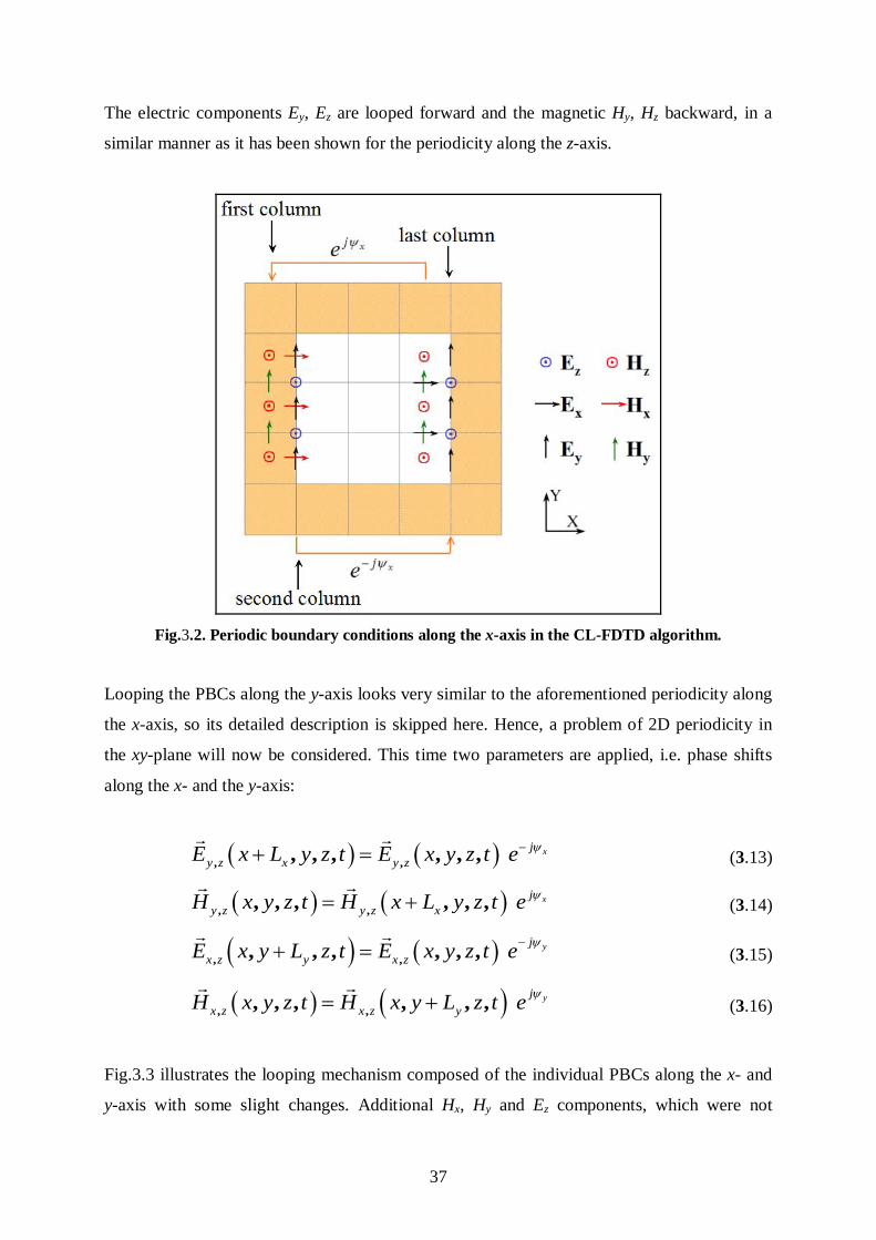
The electric components Ey, Ez are looped forward and the magnetic Hy, Hz backward, in a
similar manner as it has been shown for the periodicity along the z-axis.
Fig.3.2. Periodic boundary conditions along the x-axis in the CL-FDTD algorithm.
Looping the PBCs along the y-axis looks very similar to the aforementioned periodicity along
the x-axis, so its detailed description is skipped here. Hence, a problem of 2D periodicity in
the xy-plane will now be considered. This time two parameters are applied, i.e. phase shifts
along the x- and the y-axis:
( ) ( ), ,, , , , , , xjy z x y zE x L y z t E x y z t e ψ−+ =
(3.13)
( ) ( ), ,, , , , , , xjy z y z xH x y z t H x L y z t e ψ= +
(3.14)
( ) ( ), ,, , , , , , yjx z y x zE x y L z t E x y z t e ψ−+ =
(3.15)
( ) ( ), ,, , , , , , yjx z x z yH x y z t H x y L z t e ψ= +
(3.16)
Fig.3.3 illustrates the looping mechanism composed of the individual PBCs along the x- and
y-axis with some slight changes. Additional Hx, Hy and Ez components, which were not
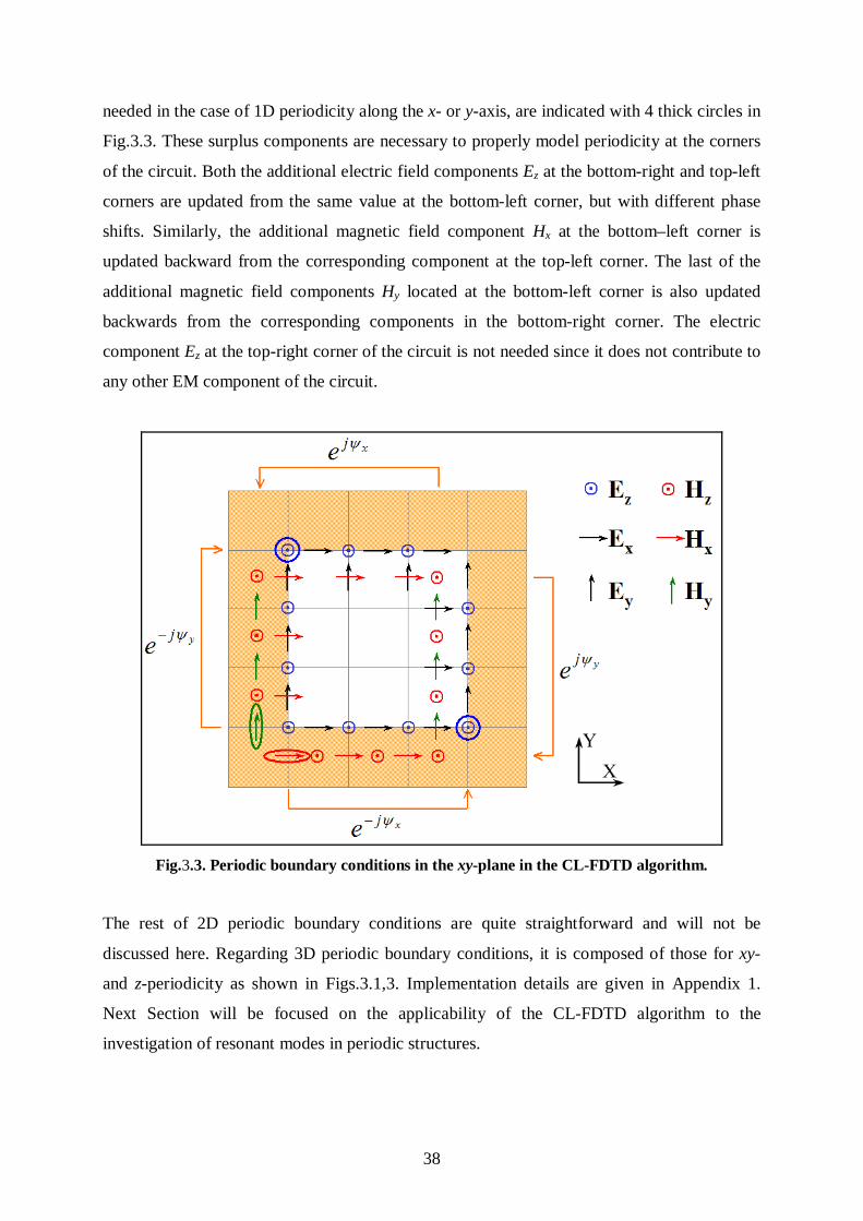
38
needed in the case of 1D periodicity along the x- or y-axis, are indicated with 4 thick circles in
Fig.3.3. These surplus components are necessary to properly model periodicity at the corners
of the circuit. Both the additional electric field components Ez at the bottom-right and top-left
corners are updated from the same value at the bottom-left corner, but with different phase
shifts. Similarly, the additional magnetic field component Hx at the bottom–left corner is
updated backward from the corresponding component at the top-left corner. The last of the
additional magnetic field components Hy located at the bottom-left corner is also updated
backwards from the corresponding components in the bottom-right corner. The electric
component Ez at the top-right corner of the circuit is not needed since it does not contribute to
any other EM component of the circuit.
Fig.3.3. Periodic boundary conditions in the xy-plane in the CL-FDTD algorithm.
The rest of 2D periodic boundary conditions are quite straightforward and will not be
discussed here. Regarding 3D periodic boundary conditions, it is composed of those for xy-
and z-periodicity as shown in Figs.3.1,3. Implementation details are given in Appendix 1.
Next Section will be focused on the applicability of the CL-FDTD algorithm to the
investigation of resonant modes in periodic structures.

39
3.4 Eigenvalue Periodic Problems
Eigenvalue problem is a notion often used not only in the formalism of linear algebra, but also
in the engineering practice. However, before concentrating on the eigenvalue problem in
electrodynamics, some algebra terms will be reminded.
Let us assume that F is a linear operator. A scalar λ is said to be the eigenvalue of F if there is
a nonzero vector r that satisfies the following equation:
rrF λ= (3.17)
Vector r that satisfies the above equation is called the eigenvector of operator F, whereas a
whole set of eigenvalues is sometimes called the spectrum of operator F. In practice, Eq.3.17
informs that operator F does not change the direction of vector r, but only rescales it by λ.
Depending on the scientific discipline concerned, vector r may be understood as a space,
function, resonant mode, quantum state etc., whereas λ denotes a scalar number, resonant
frequency or energy level of quantum state.
In particular, in electrodynamics operator F is often understood as a D’Alembert operator
222
t∂∂−∇ , and vector r as a resonant mode of an investigated circuit. In consequence, the
eigenvalue indicates a resonant frequency or a propagation constant.
A procedure of collecting eigenmodes and eigenfrequencies during EM simulation with the
CL-FDTD algorithm often proceeds as follows:
1. define a periodic structure and specify a fundamental phase shift per period;
2. excite the circuit with a wideband pulse;
3. execute the Fourier transform of the circuit impulse response (e.g. electric current
injected by the source) and search for the resonances that indicate eigenfrequencies;
4. run another simulation with a sinusoidal excitation at one of the found
eigenfrequencies to observe the eigenmode field distribution.

40
The aforementioned procedure is generally applicable to various kinds of eigenproblems’
searching. In the further investigation, two types of problems will be considered. The first
concerns 3D eigenvalue periodic problems, whereas the second refers to eigenvalue periodic
problems in the structures that belong to the already mentioned V2D class [6]. This analysis
will be useful in the modeling of a plane wave scattering from infinite periodic structures.
3.4.1 3D Eigenvalue Periodic Problems
Some practical examples of 3D eigenvalue periodic problems will now be considered, in
order to verify the accuracy of the method. A trivial scenario composed of an empty air region
terminated with a perfect electric conductor (PEC) along the y- and z-axis and with PBCs
imposed along the x-axis will be considered first. Dimensions of the air cube are 50mm x
20mm x 10mm. The aim is to find the modes that can appear in such a waveguiding structure
with no phase shift along the periodic side (ψx = 0 rad). Thus, let us put an excitation point
inside the volume and drive an Ez component with a delta pulse on the real FDTD grid. It is
quite easy to predict that the eigenmode should be observed at f = 7.5GHz. Fig.3.4 shows a
spectrum of the injected current with some resonances indicated. Indeed, the first mode is at f
= 7.49GHz, but other eigenfrequencies can also be observed. It follows from the fact that the
imposed phase shift per period xxx Lβψ = is satisfied not only for the fundamental
propagation constant 0xβ , but also for other modes usually called spatial harmonics satisfying
the following relation:
xxxn L
n πββ 20 ±= (3.18)
Fig.3.5,6 show distribution of the relevant electric and magnetic components for the modes at
f = 7.49GHz and 9.6GHz, respectively. It can be observed that there is no field variation along
periodicity (x-axis) at the first frequency, whereas electric (magnetic) field has a sine (cosine)
shape along the y-axis, due to the imposed PEC boundaries. Actually, the snapshots of these
components indicate it is a resonant mode E010. Regarding the second frequency, exactly one
period is distributed along periodicity (x-axis) and the field distribution resembles E210 mode.

41
Fig.3.4. Spectrum of the current injected into an empty air cube
(ψx = 0 rad, 50mm x 20mm x 10mm).
Fig.3.5. Distribution of Ez (left) and Hx (right) components in the xy-plane
of the real FDTD grid at f = 7.49GHz (ψx = 0 rad, 50mm x 20mm x 10mm).

42
Fig.3.6. Distribution of Ez (left), Hx (right) and Hy (bottom) components in the xy-plane
of the real FDTD grid at f = 9.6GHz (ψx = 0 rad, 50mm x 20mm x 10mm).
Let us now consider an example with a 2D periodicity. Recently, there has been
a wide and still growing interest in the so-called photonic crystals (PhCs), as they
are a specific arrangement of dielectric media resembling a solid crystal, but
in a different scale. In practice, most of PhCs find their application within
an optical spectrum as structures with 2D periodicity. Thus, let us consider
the following example of the PhC composed of a rectangular lattice of infinitely long
GaAs rods (εr = 11.56) with a radius r = 1µm and a lattice constant a = 10µm [45]
(see Fig.3.7). The aim is to extract a photonic bandgap (PBG) diagram for TM polarization
in the first irreducible Brillouin zone1
. The model is reduced to one rod only
with PBCs imposed at the lateral boundaries, whereas due to the TM polarization
the model is truncated in the xy-plane to one FDTD layer between PEC boundaries.
1 See Appendix 2.
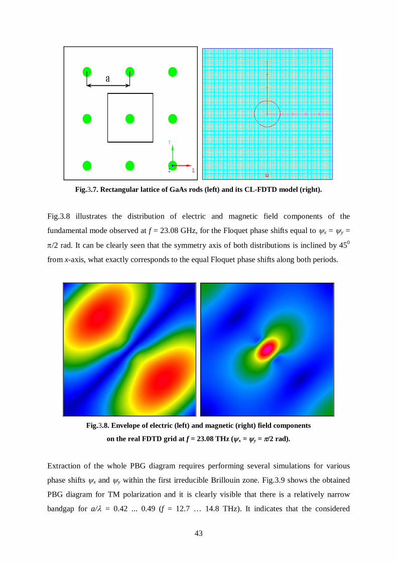
43
Fig.3.7. Rectangular lattice of GaAs rods (left) and its CL-FDTD model (right).
Fig.3.8 illustrates the distribution of electric and magnetic field components of the
fundamental mode observed at f = 23.08 GHz, for the Floquet phase shifts equal to ψx = ψy =
π/2 rad. It can be clearly seen that the symmetry axis of both distributions is inclined by 450
from x-axis, what exactly corresponds to the equal Floquet phase shifts along both periods.
Fig.3.8. Envelope of electric (left) and magnetic (right) field components
on the real FDTD grid at f = 23.08 THz (ψx = ψy = π/2 rad).
Extraction of the whole PBG diagram requires performing several simulations for various
phase shifts ψx and ψy within the first irreducible Brillouin zone. Fig.3.9 shows the obtained
PBG diagram for TM polarization and it is clearly visible that there is a relatively narrow
bandgap for a/λ = 0.42 ... 0.49 (f = 12.7 … 14.8 THz). It indicates that the considered

44
photonic crystal is opaque for a TM-polarized wave within that spectrum range, regardless of
the direction of the EM wave in the xy-plane. A comparison of the obtained PBG diagram
with the one obtained in [45] shows a good agreement. However, the results after [45] are not
shown in Fig. 3.9 to maintain legibility of the Figure.
Fig.3.9. PBG diagram (left) in the first irreducible Brillouin zone (right)
of the PhC lattice shown in Fig.3.7.
This time, a 3D rectangular photonic crystal lattice composed of silica balls (εr = 2.25) of a
radius r = 0.15µm uniformly distributed in the vacuum will be considered (see Fig.3.10). A
lattice constant is equal to a = 1µm. Let us assume that the aim is to find the fundamental
mode with zero phase shifts along three axes (ψx = ψy = ψz = 0 rad). It should be emphasized
that searching for the Floquet modes in a relatively large circuit might be a rather difficult
task. It stems from the fact that location as well as polarization of an excitation source has an
impact on its coupling with the searched modes. Thus, it is recommended to run a few
simulations for different positions of the source and for various polarizations. It should
significantly reduce the risk of missing some of the modes. Nevertheless, all of these efforts
may still be insufficient since the point source may not be able to pump energy effectively
into the circuit and, in consequence, long computing time will be needed to distinguish
eigenfreqeuncies on the spectrum of the impulse response. Therefore, sometimes it is
recommended to use a matrix of point sources to increase the coupling of the source with the

45
circuit and, in consequence, speed up the simulation. To find the Floquet modes, 5 x 5 x 5
matrix of Ez sources is set near one of the corners of the model. The rest of the procedure
follows in a similar manner as in the previous example. Fig.3.11,12 show the distribution of
electric and magnetic components in the xy- and xz-planes for the mode found at f = 590 THz.
Symmetrical distribution of the EM components can be noticed with the electric field
concentrated inside the balls and the magnetic field focused on the balls’ rim. Such
distribution satisfies the imposed phase shifts per period.
Fig.3.10. Photonic crystal lattice (a = 1µm) made of silica balls (εr = 2.25, r = 0.15µm)
located in a vacuum.
Fig.3.11. Electric (left) and magnetic (right) field components in the xy-plane at f = 590 THz.

46
Fig.3.12. Electric (left) and magnetic (right) field components in the xz-plane at f = 590 THz.
The goal of the next example is to evaluate 3D periodic boundary conditions implemented in
the CL-FDTD algorithm. It will be validated against the plane wave expansion method as one
of the computational techniques for the analysis of dispersive properties of photonic crystals
[46]. The example is taken from [47], where the authors consider a three-dimensional body
centered cubic (bcc) lattice2
processed in a dielectric material with a relative permittivity εr =
25. Let us set the lattice constant to a = 0.6 µm. The bcc shape is made using an air cube with
a side length 0.75a, cut in its center and in each corner of a dielectric bulk (see Fig.3.13).
Fig.3.13. Single cell of the rectangular body centered cubic lattice (εr = 25, a = 0.6µm).
2 See Appendix 2.

47
The cell size in the CL-FDTD model of the considered bcc lattice is set to 20nm.
Periodic boundary conditions are applied along three Cartesian axes. The procedure
for PBG diagram collection is exactly the same as recalled during the analysis
of the structure shown in Fig.3.8. Special care must be taken with the location
of the excitation source. Its improper location may result in weak coupling
with some of the lattice modes. Therefore, the analysis has been performed twice,
with different locations of the point source in order to double-check whether
all the modes were found. Fig.3.14 shows the obtained PBG diagram of the bcc lattice.
It may be noticed that a complete band gap occurs for a/λ = 0.374…0.382.
Comparison against the results from [47] shows a good agreement, though it was not plotted
to maintain legibility of the Figure.
Fig.3.14. PBG diagram (left) in the first irreducible Brillouin zone (right)
of the body centered cubic lattice shown in Fig.3.13.
To summarize this Section, periodic boundary conditions introduced in the CL-FDTD
algorithm along the three Cartesian axes enable the investigation of Floquet modes
in periodic structures. Author’s contribution includes the extension of PBCs presented
in [20] for 1D to 2D and further 3D periodicity. Presented examples confirm the validity
of the implemented algorithms.

48
3.4.2 V2D Eigenvalue Periodic Problems
The issue of electromagnetic problems belonging to V2D class has been briefly addressed at
the beginning of Chapter 3.2. The V2D FDTD algorithm is often useful for preliminary
computation at input and output ports of the circuit. The obtained solution can further be
coupled to a whole 3D circuit as an excitation source, or a load matched to the particular
mode. Such an approach significantly simplifies the analysis as well as the understanding of
the phenomenon of wave propagation in the waveguiding structures. In general, the procedure
is as follows:
1. Wideband simulations are performed for all input and output ports defined in the
circuit. For that purpose, each port – understood as the cross-section layer of the
waveguide feed or load – is modeled as a V2D circuit and the distribution of the
propagating mode is searched for a fixed longitudinal phase constant βf assumed by
the user. In case of typical waveguides such as the rectangular one, dispersive
behavior of the modes is analytically known, so the whole procedure for the mode
searching can be fully automated, like in QuickWave-3D software package [48].
2. Once the frequency associated with the particular mode is found, the V2D port is
excited with a sinusoidal signal to determine the distribution of electromagnetic
components tangential to the port plane, commonly called "mode template".
3. Afterwards, the original 3D circuit is excited with the already pre-processed mode
template multiplied by the user-defined time-varying signal (sinus, pulse, Gauss, etc.).
4. Eventually, during the simulation run, a scattering matrix is iteratively calculated at
the reference planes shifted a few FDTD cells into the circuit with respect to the
considered ports.
The advantage of using the aforementioned procedure is the possibility to excite and scan
each waveguide mode independently. Thus, one may analyze and control the power
distribution on all modes and between them.
The goal of this work is not to investigate the mode template generation in its classical form
since it was thoroughly developed some years ago [6]. The aim is rather to show that the
mode template computation may be extended to V2D FDTD circuits with periodic boundary

49
conditions applied. As it will be further shown, it will be a useful tool in the modeling of EM
wave scattering from periodic structures.
The algorithm of looping periodic boundary conditions is exactly the same as for 3D FDTD
circuits (see Chapter 3.2). Let us first consider 22mm x 10mm rectangular air-box set in the
xy-plane and discretized with 0.5mm FDTD cell size, assuming that the modes with zero
longitudinal phase constant (βf = 0 rad/mm) and zero phase shift per period along the x-axis
(ψx = 0 rad) are searched for. The model is terminated with PEC boundaries along the y-axis.
Such boundary conditions clearly indicate that the only possible propagation is along
periodicity, that is x-axis. Thus, exciting the circuit with Ey polarized point source, the
associated Hz magnetic field component can be expected.
Fig.3.15. Spectrum of the electric current injected into a rectangular air-box
(ψx = 0 rad, βf = 0 rad/mm).
Due to the chosen source polarization and the boundary conditions imposed on the circuit, the
first propagating mode can be expected to be of TEM kind operating at the wavelength equal
to the period of the circuit, that is λ0 = 22 mm (f0 = 13.64 GHz). Indeed, spectrum of the
impulse response of the considered scenario, shown in Fig.3.15, confirms with 0.15%
accuracy the theoretical prediction, whereas field distribution of relevant components snapped
at this frequency ensures that this is a TEM mode propagating along the x-axis (see Fig.3.16).
Similarly, the next mode is supposed to propagate at f1 = 27.27 GHz corresponding to the

50
wavelength twice shorter than the circuit period, i.e. λ1 = 11 mm. Obviously, it also satisfies
periodic boundary conditions but with a phase shift ψx = 0 + 2π. The discrepancy between the
obtained result and theoretical calculation is somewhat larger than for the previous mode and
amounts to 0.33% – apparently due to inherent dispersion of the FDTD algorithm increasing
with frequency.
Fig.3.16. Snapshots of the electric Ey (left column) and magnetic Hz (right column) components
at both f1 = 13.62GHz (top row) and f2 = 27.18GHz (bottom row) modes indicated in Fig.3.15.
Such a canonical example was introduced to test validity of the V2D FDTD algorithm
coupled with periodic boundary conditions. Yet, it is still needed to be verified how it will
operate for a nonzero longitudinal phase constant. Let us consider the same geometry, but this
time the objective is to obtain an oblique propagation of Ey polarized plane wave at α = 600
angle counted from the longitudinal z-axis. The operating frequency is equal to f = 20 GHz.
The well-known relation:
2222zyx ββββ ++= (3.19)

51
can be used to determine both the longitudinal phase constant βf and the phase shift per period
ψx. In the considered case, there is no phase variation along the y-axis, so βy = 0 rad/mm. The
longitudinal phase constant βf used in the V2D FDTD algorithm corresponds directly to βz,
whereas the fundamental phase shift per period is given by ψx = βx Lx. Thus, knowing the
frequency and the incident angle, it can be determined that:
( ) mmradzf 20944.0cos === αβββ (3.20)
( ) radLL xxxx 9807.7sin === αββψ (3.21)
Fig.3.17. Spectrum of the electric current injected into a rectangular air-box
(ψx = 7.9807 rad, βf = 0.20944 rad/mm).
Fig.3.17 indicates resonance at the frequency f = 19.98 GHz (λ = 15.01 mm), which is 0.1%
lower than anticipated. The distribution of the electric field component Ey at that frequency is
shown in Fig.3.18. The measured wavelength along the x-axis is equal to λx = 17.4 mm, so by
applying Eq.3.21, it can be derived that the angle of incidence equals to α = 59.60. In fact,
major contribution to the obtained discrepancy of 0.67% follows from the uncertainty of the
wavelength measurement due to finite discretization of the FDTD model. Dispersion of the
FDTD algorithm is at least one order of magnitude smaller since 30 FDTD cells per
considered wavelength have been applied.

52
Fig.3.18. Snapshot of the electric component Ey at f1 = 19.98GHz
for the mode indicated in Fig.3.17.
The analysis presented above confirms the possibility of using periodic boundary conditions
in a V2D FDTD model. The investigation of this will be recalled again in the next Chapter,
when modeling of the scattering from periodic structures will be addressed.
3.5 FDTD Modeling of Scattering from Periodic Structures
The next issue has been under thorough investigation by the author of this dissertation during
his studies and concerns the phenomenon of electromagnetic wave diffraction on a periodic
structure. In principle, this is no longer an eigenvalue problem but a deterministic one since
the structure is exposed to an independent external source of EM radiation. The author’s
interest in this subject results from the recent dynamic development of sophisticated
metrology methods based on the diffraction phenomenon, where the FDTD method has found
its application. As an example, let us recall here a scatterometry technique [49] commonly
applied to the measurement and control of characteristic features during the lithography
process of integrated circuits (IC) of large-scale integration (LSI). Another example refers to
the frequency selective structures (FSS) exploited as selective-angle antennas or reflective
surfaces [50]. Let us point out an advantage of the CL-FDTD algorithm in the modeling of the
aforementioned scattering problems. Solutions for some practical scenarios will be shown in
comparison to the other numerical methods, such as Finite Element Method Time-Domain
(FETD) [51] or Rigorous Coupled Wave Analysis (RCWA) [52].

53
In general, the problem of electromagnetic wave scattering from a periodic structure may be
split into four separate cases:
1. infinite structure and infinite spot,
2. finite structure and infinite spot,
3. infinite structure and finite spot,
4. finite structure and finite spot.
To be precise, the assumption imposed in the fourth case is always true
in the real problems, but often leads to impractically large requirements
for computer resources. Therefore, other approaches may be some interesting
alternatives provided that the achieved speedup is not at the cost of accuracy
of the final solution. For the purpose of this thesis, all mentioned
approaches will be addressed to assess their computational capabilities and
a range of applicabilities, except the third one since it has already been investigated in
[42],[43].
Let us first specify some useful notions. Fig.3.19 illustrates a definition of two polarizations
which will be exploited in the modeling of scattering phenomenon:
- TE (σ) with an electric field transverse to an incidence plane,
- TM (π) with a magnetic field transverse to an incidence plane.
It should be emphasized that the aforementioned notation of an EM wave polarization used
for the scattering problems, often applied in the scatterometry, differs from the definition
known in the analysis of eigenvalue and waveguiding problems.
Both incident (αinc) and reflection (αm) angles are measured from the normal (see the dashed
line in Fig.3.19). It is often assumed in the analysis of diffraction gratings, such as
the one shown in Fig.3.19, that the angles on the left-hand side of the normal
are positive, whereas those on the right-hand side are negative. Let us recall that
if a ray illuminates a periodic structure at a particular angle of incidence it may be
reflected not only at the specular angle α0 = -αinc, also called 0th diffraction order.
There may also occur non-evanescent higher diffraction orders (m = 1, 2…).
A reflection angle of the mth diffraction order can be determined reminding that, in general:

54
( )β
βα mx
m =sin (3.22)
where βx m denotes the phase constant component along the x-axis of the mth diffraction order.
Then, following Eq.3.18, a Bragg condition can be obtained:
( ) ( )L
mmincλαα =+ sinsin (3.23)
provided that β ≥ βx m.
Fig.3.19. TE (left) and TM (right) polarization of an incident wave.
It will be later shown that the aforementioned equation may be derived directly from the
Floquet theorem. Eq.3.23 refers to the 1D case and indicates that higher diffraction orders can
appear when the operating wavelength λ is short enough and becomes comparable with the
fundamental period of the structure L. Moreover, as the angle of incidence increases, more
diffraction orders may be observed. Let us recall, as an example, scattering of light ray from a
solid crystal bulk. Only specular reflection can be observed since the lattice constant (L <
0.5nm) is of the order of magnitude smaller than the shortest wavelength in the visible
spectrum region (λ > 400nm). However, when using X-ray with the wavelengths comparable
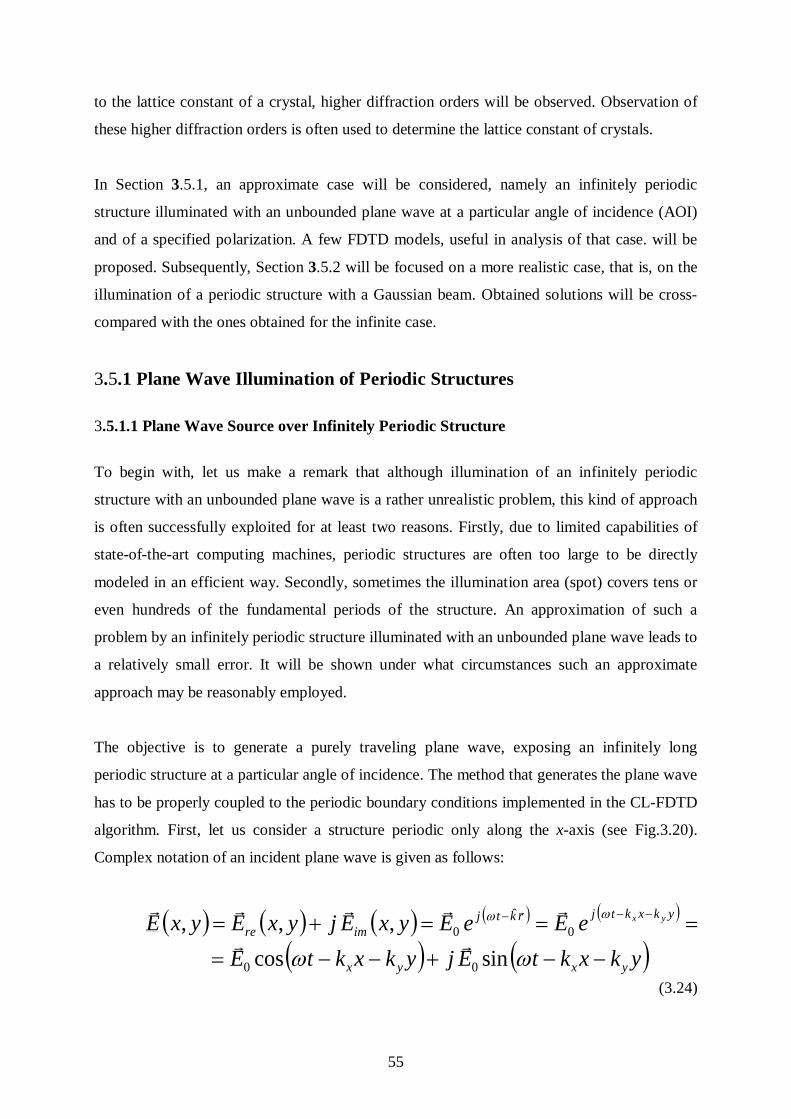
55
to the lattice constant of a crystal, higher diffraction orders will be observed. Observation of
these higher diffraction orders is often used to determine the lattice constant of crystals.
In Section 3.5.1, an approximate case will be considered, namely an infinitely periodic
structure illuminated with an unbounded plane wave at a particular angle of incidence (AOI)
and of a specified polarization. A few FDTD models, useful in analysis of that case. will be
proposed. Subsequently, Section 3.5.2 will be focused on a more realistic case, that is, on the
illumination of a periodic structure with a Gaussian beam. Obtained solutions will be cross-
compared with the ones obtained for the infinite case.
3.5.1 Plane Wave Illumination of Periodic Structures
3.5.1.1 Plane Wave Source over Infinitely Periodic Structure
To begin with, let us make a remark that although illumination of an infinitely periodic
structure with an unbounded plane wave is a rather unrealistic problem, this kind of approach
is often successfully exploited for at least two reasons. Firstly, due to limited capabilities of
state-of-the-art computing machines, periodic structures are often too large to be directly
modeled in an efficient way. Secondly, sometimes the illumination area (spot) covers tens or
even hundreds of the fundamental periods of the structure. An approximation of such a
problem by an infinitely periodic structure illuminated with an unbounded plane wave leads to
a relatively small error. It will be shown under what circumstances such an approximate
approach may be reasonably employed.
The objective is to generate a purely traveling plane wave, exposing an infinitely long
periodic structure at a particular angle of incidence. The method that generates the plane wave
has to be properly coupled to the periodic boundary conditions implemented in the CL-FDTD
algorithm. First, let us consider a structure periodic only along the x-axis (see Fig.3.20).
Complex notation of an incident plane wave is given as follows:
( ) ( ) ( ) ( ) ( )
( ) ( )ykxktEjykxktEeEeEyxEjyxEyxE
yxyx
ykxktjrktjimre
yx
−−+−−=
===+= −−−
ωω
ωω
sincos,,,
00
0ˆ
0
(3.24)

56
Fig.3.20. Oblique incidence of a plane wave in the xy-plane
on the structure periodic along the x-axis.
Eq.3.24 indicates that in order to obtain a purely traveling plane wave, an imaginary FDTD
grid has to be excited in quadrature to the real one. Thus, the following delay between the
excitation of both grids has to be imposed:
0
0
41
4 fT
t ==∆ (3.25)
In consequence, on both grids the plane waves shifted by the quarter of wavelength should be
observed. Fig.3.21 shows the proposed FDTD model of plane wave generation in a scenario
with periodic boundary conditions. The model is truncated with Mur superabsorption at the
top and at the bottom. Below the top superabsorption, there is a wall defined along the whole
length of the model, where the plane wave is supposed to be excited downwards.
Furthermore, below the plane wave wall (PLW) in a total field region, another wall is set,
sometimes called a “Huygens surface”, where near to far (NTF) field transformation is to be
performed. It allows watching both incident and scattered rays. In QuickWave-3D
commercial software package [48] used for that analysis, the direct Fourier transform (DFT)
is applied instead of the fast Fourier transform (FFT), commonly used for the NTF
transformation. As a result of that kind of approach, the user can easily control convergence
of the solution as the simulation continues. If the aim is to consider the TE (TM) polarization,
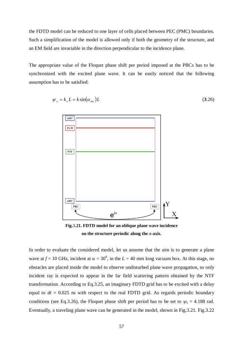
57
the FDTD model can be reduced to one layer of cells placed between PEC (PMC) boundaries.
Such a simplification of the model is allowed only if both the geometry of the structure, and
an EM field are invariable in the direction perpendicular to the incidence plane.
The appropriate value of the Floquet phase shift per period imposed at the PBCs has to be
synchronized with the excited plane wave. It can be easily noticed that the following
assumption has to be satisfied:
( )LkLk incxx αψ sin== (3.26)
Fig.3.21. FDTD model for an oblique plane wave incidence
on the structure periodic along the x-axis.
In order to evaluate the considered model, let us assume that the aim is to generate a plane
wave at f = 10 GHz, incident at α = 300, in the L = 40 mm long vacuum box. At this stage, no
obstacles are placed inside the model to observe undisturbed plane wave propagation, so only
incident ray is expected to appear in the far field scattering pattern obtained by the NTF
transformation. According to Eq.3.25, an imaginary FDTD grid has to be excited with a delay
equal to dt = 0.025 ns with respect to the real FDTD grid. As regards periodic boundary
conditions (see Eq.3.26), the Floquet phase shift per period has to be set to ψx = 4.188 rad.
Eventually, a traveling plane wave can be generated in the model, shown in Fig.3.21. Fig.3.22
58
shows the electric field distribution on both the real and imaginary FDTD grids snapped at the
same time instant. Looking carefully on both snapshots, it can be noticed that the plane waves
are indeed shifted by the quarter of the wavelength with respect to each other. Nevertheless, it
should be emphasized that the CL-FDTD method is frequency selective, in a sense that a
wideband excitation will not produce a traveling plane wave in the whole band due to the
unsatisfied Floquet phase condition for the frequencies different than the matched one. This is
the main limitation of the method. More discussion of these issues will be presented later in
this thesis.
Fig.3.22. Plane wave illumination at the real (left) and imaginary (right) FDTD grids
at f = 10GHz, incident at αinc = 300, snapped at the same time instant.
Now, in order to evaluate the diffraction of a plane wave from a periodic structure we can
place it inside the proposed model. However, one should be aware that – according to
Fig.3.21 – reflection coefficient is extracted with the aid of the NTF transformation. Thus,
there is still the issue, how to understand the scattering pattern obtained from NTF
computation. In principle, a far-field radiation beam of an infinite plane wave is of Dirac delta
shape since the angle of incidence of such infinite beam is exactly defined. However, due to
the fact that an NTF surface is exactly equal the length of the FDTD model, calculated beams
will be significantly broadened. From a mathematical point of view, obtained beam is a
convolution of a window function and the Dirac delta. In that case, the window function

59
reflects the spatial length of the NTF surface applied in the model shown in Fig.3.21.
Therefore, it should be determined whether a finite length of the NTF surface disturbs the
extraction of incident and reflected beams in the scattering pattern.
Let us assume that the aim is to excite a plane wave at a particular frequency f, incident at the
angle αinc, in the periodic model of length L. Following Eq.3.26, a proper Floquet phase shift
per period ψx can be set. Thus, a generated plane wave has the following form (compare
Eq.3.24):
( ) ( )yxtj yxeyxE 00, ββω −−=
(3.27)
where
( )incx αββ sin0 = (3.28)
( )incy αββ cos0 −= (3.29)
The far-field scattering pattern is calculated at the NTF level in the following way:
( ) ( ) ( )∫−
−=2/
2/
sin,L
L
xj dxeyxEE αβα
(3.30)
Substituting Eqs.3.27-29 to Eq.3.30 and solving the given integral, the following formula can
be obtained:
( ) ( ) ( )w
wLeE ytj y sin0βωα −=
(3.31)
where
( ) ( )[ ]ααλ
π sinsin += incLw (3.32)

60
Eventually, it can be noticed from Eq.3.31,32 that zeros of the far-field scattering pattern are
obtained if and only if the following relation is satisfied:
( ) ( )L
mincλαα =+ sinsin (3.33)
where m = ±1, ±2, …
In principle, the above formula states a Bragg condition and enables us to evaluate higher
diffraction orders (compare Eq.3.23). It proves that the incident beam in the scattering pattern,
though broadened, does not disturb values at higher diffraction angles since they appear
exactly at the minima of the incident beam extracted using NTF transformation. The same
investigation may be performed to make sure that the higher diffraction rays do not interfere
with each other as well. To conclude, it has been formally proven that as long as NTF
transformation is computed over a length equal to the multiple of the fundamental period of
the structure, only discrete points in the scattering pattern which satisfy Eq.3.33 are calculated
without any interference. Moreover, increase of NTF length L results in narrower beams and
raising maxima. In consequence, NTF transformation executed in CL-FDTD model provides
– within numerical accuracy of the method – exact values of the far-field electric field
intensities at both incident and reflected angles.
To confirm the considerations carried out above, let us look at the angular scattering pattern
processed by NTF transformation, shown in a logarithmic scale in Fig.3.23, and obtained for
the empty air region already considered in Fig.3.22. The allowed diffraction angles are
marked with vertical dashed lines. The angular variable φ used in the figures below is the
azimuth angle in the xy-plane counted counterclockwise from the x-axis. It can be expected
that an illumination beam appears at φ = 3000, what corresponds to αinc = 300, using the notion
defined in Fig.3.20. It can be also noticed that, although the center of the incident beam is not
exactly at 3000, all minima fit exactly to the angles of potentially allowed higher diffraction
orders. In particular, there is a significant minimum at φ = 600, which corresponds to a
specular reflection angle. If any obstacle is put inside the model, another beam centered at φ =
600 will appear, but it will surely not disturb the value of the incident beam at φ = 3000.

61
Consequently, reflection coefficient, understood as the ratio of electric field intensities at 600
and 3000 angles, will be calculated correctly.
Fig.3.23. Scattering pattern shown in a logarithmic scale for the plane wave
incident at αinc = 300 (φinc = 3000) in an empty air region (f = 10GHz, L = 40mm).
Fig.3.24. Scattering patterns for the plane wave incident at αinc = 300 in an empty air region
with a varying length L (f = 10GHz, L = N*40mm).

62
Table 3.1. Maximum electric field intensities of the incident beams shown in Fig.3.24.
N |E| @ φ = 3000 [ mW ] ∆φ3dB
1 0.608 42.2
2 1.223 21.8
4 2.454 10.9
Fig.3.24 illustrates what happens when NTF transformation is performed over one, two and
four periods of the structure. Table 3.1 presents the maximum electric field intensities of
incident beams with a growing number of structure periods and the corresponding 3dB beam
widths. It confirms that the width of a beam is inversely proportional, and its height linearly
varies with the length of NTF transformation surface. As anticipated before in this Chapter,the
beam finally converges to the Dirac delta.
Let us now consider EM plane wave scattering from a particular periodic structure. Fig.3.25
shows the geometry of the scenario. It is a periodic set of crosses made of perfect electric
conductor (PEC) buried in a dielectric (ε1 = 2.56 ε0). Fundamental period is equal to d = 100
mm. The objective is to expose the structure to a plane wave, incident at αinc = 300 within a
range of d/λ0 = 0 ... 1 and, afterwards, extract a specular reflection coefficient.
Fig.3.25. Dielectric coated PEC cross-shaped grating (d = 100 mm, ε1 = 2.56 ε0).
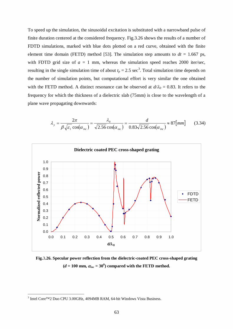
63
To speed up the simulation, the sinusoidal excitation is substituted with a narrowband pulse of
finite duration centered at the considered frequency. Fig.3.26 shows the results of a number of
FDTD simulations, marked with blue dots plotted on a red curve, obtained with the finite
element time domain (FETD) method [53]. The simulation step amounts to dt = 1.667 ps,
with FDTD grid size of a = 1 mm, whereas the simulation speed reaches 2000 iter/sec,
resulting in the single simulation time of about tp = 2.5 sec3
. Total simulation time depends on
the number of simulation points, but computational effort is very similar the one obtained
with the FETD method. A distinct resonance can be observed at d/λ0 = 0.83. It refers to the
frequency for which the thickness of a dielectric slab (75mm) is close to the wavelength of a
plane wave propagating downwards:
( ) ( ) ( )[ ]mmd
incincincy 87
cos56.283.0cos56.2cos2 0
1
≈===αα
λαεβ
πλ (3.34)
Dielectric coated PEC cross-shaped grating
0.0
0.1
0.2
0.3
0.4
0.5
0.6
0.7
0.8
0.9
1.0
0.0 0.1 0.2 0.3 0.4 0.5 0.6 0.7 0.8 0.9 1.0
d/λ0
Nor
mal
ized
ref
lect
ed p
ower
FDTDFETD
Fig.3.26. Specular power reflection from the dielectric-coated PEC cross-shaped grating
(d = 100 mm, αinc = 300) compared with the FETD method.
3 Intel Core™2 Duo CPU 3.00GHz, 4094MB RAM, 64-bit Windows Vista Business.

64
It seems to be a full-wave resonance. Similarly, what can be easily verified, there is a half-
wave resonance at d/λ0 = 0.5. However, even with a very long computation and much finer
meshing, it was not be possible to detect the resonance near d/λ0 = 0.61. Supposedly, it was a
spurious solution of the benchmarking FETD method which appeared in [53].
Fig.3.27. Angular scattering pattern in power scaling
for the dielectric-coated PEC cross-shaped grating (d = 100 mm, αinc = 300, f = 1.2GHz)
obtained in one (red) and ten (blue) periods model.
Table 3.2. Values taken from the angular scattering pattern shown in Fig.3.27.
N |E|2 @ φ = 600 [ 2mW ] |E|2 @ φ = 3000 [ 2mW ] RP
1 0.037417 0.160685 0.23286
10 3.778596 16.220854 0.23295
Let us now observe the angular scattering pattern (ASP) for d/λ0 = 0.4, obtained using
NTF transformation performed in two models which consist of one and ten
fundamental periods of the considered grating structure. Fig.3.27 clearly indicates
that for the one-period model (the red curve and the left scale) – due to a relatively

65
short length of the model – ASP is substantially broadened, so it is hard to distinguish
incident and reflected beams. Nevertheless, comparison with the ten-period case
(the blue curve and the right scale) shows that, though the shape of ASP
may be somewhat confusing, it provides accurate values at the diffraction angles (compare
Eq.3.33).
The values presented in Table 3.2 indicate that the difference between the specular
power reflection coefficients obtained in both short and long models is about 0.01%,
mainly due to the discrete FDTD meshing. Moreover, it can be also noticed that
the intensities of incident and reflected beams are ten times higher in the model
consisting of ten periods of the structure, which is a direct consequence of ten times wider
domain of integration.
Now, let us return to the issue of narrowband properties of the plane wave excitation
model implemented in the CL-FDTD algorithm. As it has been mentioned earlier,
undisturbed traveling plane wave in a periodic structure can be obtained only for
a discrete frequency. In consequence, to obtain a reflection coefficient in the specified
spectrum range, as shown in Fig.3.26, several simulations have to be run
for consecutive frequency points. Let us look for the possibilities of alleviating such
a strict condition. The considered dielectric-coated PEC cross-shaped grating will be
excited with a wideband pulse and the reflection coefficient will be extracted in the vicinity of
the matched frequency, in order to assess the reflection coefficient error introduced by
imperfect plane wave excitation.
Fig.3.28 presents the simulation results obtained for the dielectric-coated PEC
cross-shaped grating at a few frequency sub-bands. Most of all, it can be noticed
that discrepancies are not systematic, so it is hard to draw general conclusions
about inaccuracy. Nevertheless, it can be concluded that the deviation from
the matched frequency by more than about 2-3% is not acceptable if accuracy of
the obtained result is expected to be less than 5%. In consequence, there is not much
room to maneuver, especially when considering a real electromagnetic design, where
the aim is usually to achieve accuracy much below 1%. It brings us back to the starting point,
that is, to the single frequency approach.
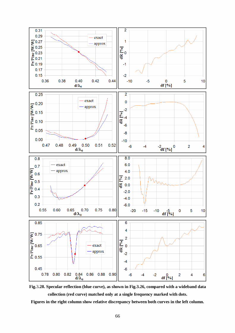
66
Fig.3.28. Specular reflection (blue curve), as shown in Fig.3.26, compared with a wideband data
collection (red curve) matched only at a single frequency marked with dots.
Figures in the right column show relative discrepancy between both curves in the left column.

67
Now, let us consider another example of 1D periodic structure, showing a little different
scope of potential applicability for the CL-FDTD algorithm. This time, a so-called poly-to-
active stack [54], composed of two diffraction gratings and processed in different layers on a
silicon wafer during a lithography process of integrated circuits (IC), will be considered (see
Fig.3.29). These kinds of stacks are exploited as test targets in a scatterometry technique [49],
applied to control accuracy and precision of the lithography process.
Fig.3.29. Cross-section view of a poly-to-active stack.
In principle, scatterometry is a very interesting method, which is very useful when the
dimensions of features processed with the lithography are much below the resolution limit of
imaging techniques. The idea of scatterometry is to expose a target to a ray of bright light
incident at a particular angle and, afterwards, to collect the spectrum of reflection coefficient
(usually specular one), which is supposed to contain information about the geometry of the
illuminated target. It may be the width of a line or a trench, the shift (overlay) between layers
processed on a wafer, etc. However, to increase the signal to noise ratio (SNR) of the
scatterometry technique, the target is usually periodically repeated to enhance the gain of the
reflected ray. Thus, the length of the target is of the order of tens of microns – depending
mainly on the diameter of the illumination spot. In the example below, a TE polarized plane
wave (see Fig.3.19) incident at the angle of 250, on a target with the fundamental period
(pitch) of 320nm, will be investigated. The width of the lines and the trenches, sometimes
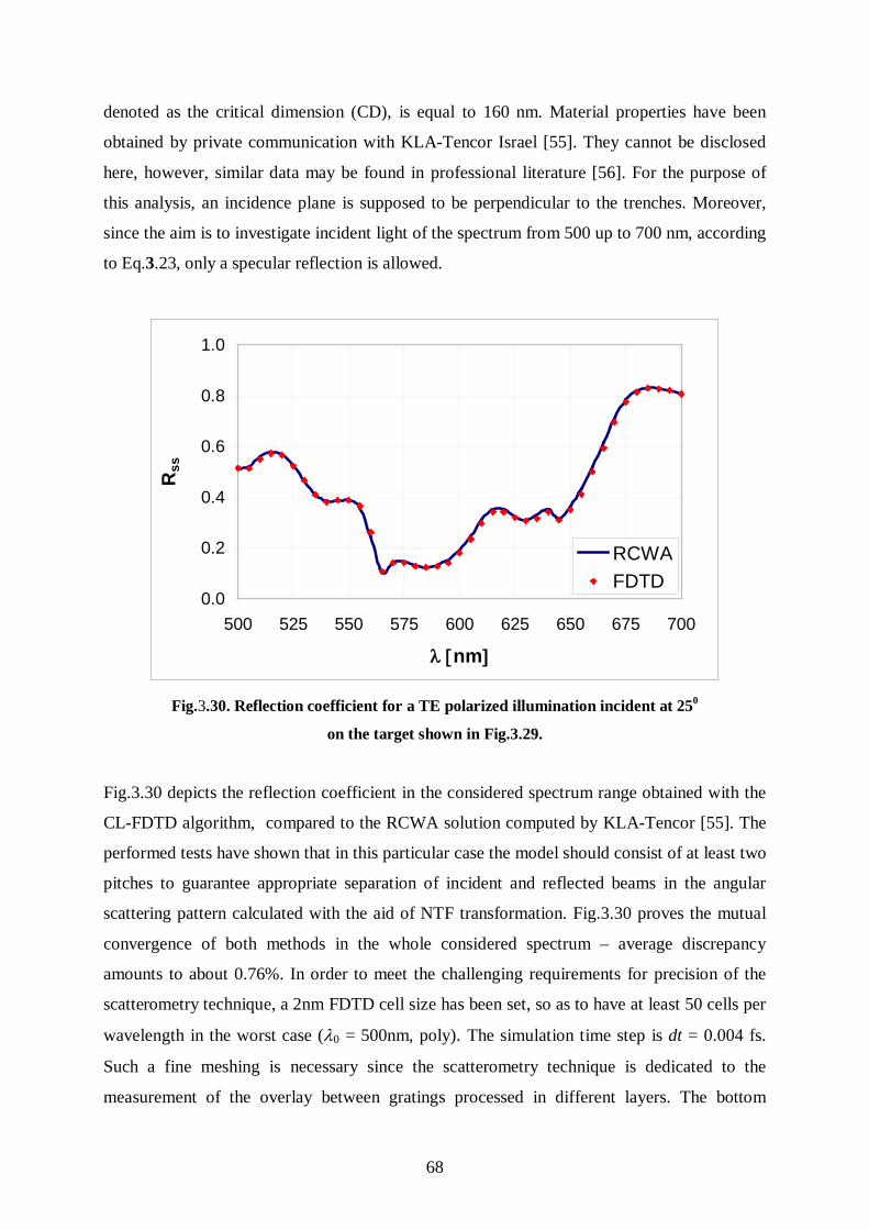
68
denoted as the critical dimension (CD), is equal to 160 nm. Material properties have been
obtained by private communication with KLA-Tencor Israel [55]. They cannot be disclosed
here, however, similar data may be found in professional literature [56]. For the purpose of
this analysis, an incidence plane is supposed to be perpendicular to the trenches. Moreover,
since the aim is to investigate incident light of the spectrum from 500 up to 700 nm, according
to Eq.3.23, only a specular reflection is allowed.
0.0
0.2
0.4
0.6
0.8
1.0
500 525 550 575 600 625 650 675 700
λ [nm]
Rss
RCWAFDTD
Fig.3.30. Reflection coefficient for a TE polarized illumination incident at 250
on the target shown in Fig.3.29.
Fig.3.30 depicts the reflection coefficient in the considered spectrum range obtained with the
CL-FDTD algorithm, compared to the RCWA solution computed by KLA-Tencor [55]. The
performed tests have shown that in this particular case the model should consist of at least two
pitches to guarantee appropriate separation of incident and reflected beams in the angular
scattering pattern calculated with the aid of NTF transformation. Fig.3.30 proves the mutual
convergence of both methods in the whole considered spectrum – average discrepancy
amounts to about 0.76%. In order to meet the challenging requirements for precision of the
scatterometry technique, a 2nm FDTD cell size has been set, so as to have at least 50 cells per
wavelength in the worst case (λ0 = 500nm, poly). The simulation time step is dt = 0.004 fs.
Such a fine meshing is necessary since the scatterometry technique is dedicated to the
measurement of the overlay between gratings processed in different layers. The bottom

69
grating is often buried below some opaque material, such as poly or barc (see Fig.3.29),
resulting in ill-conditioned algorithm for the overlay extraction. However, even with such a
fine discretization, a simulation of one frequency point is relatively quick and the
convergence is reached after 580 seconds, achieving the simulation speed of about 100
iter/sec4
. Successful comparison of the new algorithm with the calculations performed using
the RCWA method justifies the first statement of the thesis posed in Chapter 1.
The author of this thesis has been involved in a European project [57], where his aim was to
develop and implement FDTD models applicable to the modeling of scatterometry of periodic
structures. More details concerning this issue are omitted here and can be found in
[49],[54],[58-60].
Now, let us consider an oblique incidence of a plane wave on a two-dimensionally periodic
structure to verify the 2D PBC algorithm implemented by the author of this thesis5. First,
relations between the Floquet phase shift per period in each direction and the incidence angle
will be introduced. Let us apply a spherical coordinate system6
to maintain generality of the
notation. It should be emphasized that in the modeling of a plane wave scattering
phenomenon, the Floquet phase shift per period along an arbitrary axis may be understood as
the phase shift of the considered plane wave along one period of the FDTD model. Thus, the
relevant formulae are as follows:
( ) ( ) xxxx LkLk θφψ sincos== (3.35)
( ) ( ) yyyy LkLk θφψ sinsin== (3.36)
( ) zzzz LkLk θψ cos== (3.37)
To exemplify the issue, let us consider an infinite set of 10mm x 10mm metal patches set in
the xy-plane, located in an empty air region. The fundamental period is the same in both
directions and amounts to 20mm. The goal is to illuminate these patches with a TE polarized
plane wave (see Fig.3.19), of the frequency f = 20 GHz, and incident at (φ, θ) = (450, 1350).
The operating frequency imposes a delay between excitation signals of real and imaginary
FDTD grids of dt = T/4 = 12.5 ps (see Eq.3.25). 4 Intel Core™2 Duo CPU 3.00GHz, 4094MB RAM, 64-bit Windows Vista Business. 5 See Appendix 1. 6 See Appendix 3.

70
Two simulations with 1x1 and 2x2 arrays of metal patches will be performed – both with
periodic boundary conditions imposed. For the purpose of this analysis, a 0.25 nm FDTD cell
size has been set (60 cells/λ) to suppress potential problems with the numerical dispersion of
the FDTD algorithm. Fig.3.31 depicts normalized scattering patterns obtained at the incident
plane (θ = 450). The specular reflection is accompanied by the 1st order one, appearing at (φ,
θ) = (450, 339.30) (compare Eq.3.23). When inspecting the curve obtained for 1x1 model
(red), one may notice a significant deformation of the beam. Nevertheless, comparison with
the plot obtained for 2x2 array model (blue) once again confirms the theoretical findings
presented earlier (see Eq.3.33) that the beam deformation due to a finite length of an NTF
surface does not disturb the scattering pattern at the angles belonging to a set of diffraction
orders. Comparing both characteristics plotted in Fig.3.31, the discrepancy of the reflection
coefficient of the 0th order is about 0.11%, whereas for the 1st order, it amounts to 0.23% (see
values in Table 3.3).
Fig.3.31. Angular scattering patterns (normalized power scaling) calculated in an incident plane
for the infinite array of 10mm x 10mm metal patches modeled with
1x1 (red) and 2x2 (blue) matrix of patches.
71
Table 3.3. Values taken from the angular scattering patterns shown in Fig.3.31.
N |E|2 @ θ = 450 |E|2 @ θ = 1350 |E|2 @ θ = 3390 RP (450/1350) RP (3390/1350) 1x1 0.093498 0.948897 0.089128 0.098534 0.093928 2x2 0.095949 0.984369 0.090183 0.097472 0.091615
To resume, extraction of the far-field angular scattering pattern due to a plane wave incidence
has been discussed. The proposed approach allows evaluation of not only the specular
diffraction from a periodic structure, but also possible higher diffraction orders. The author
has successfully implemented and verified a plane wave source and a near-to-far
transformation in the presence of periodic boundary conditions in the CL-FDTD algorithm,
proving the first statement of the thesis posed in Chapter 1.
3.5.1.2 Waveguide Mode over Infinitely Periodic Structure
Now, let us introduce a different method applicable to the analysis of EM wave scattering
from infinite periodic structures. An analogy to the wave propagation in a waveguide will be
applied. Let us first remind that each E(H)mn mode in a rectangular waveguide has a priori
known forward phase constant [61]:
22mncmnf βββ −= (3.38)
where β stands for the phase constant in an unbounded region and βc mn is the cut-off of the
considered mode. Each mode has a specified distribution of EM components in a waveguide
cross-section, which does not depend on frequency. Such a distribution is usually called a
mode template. It will be shown that such a mode template resembles a standing wave in an
unbounded region.
Let us consider – without loss of generality – modes only of E(H)m0 kind. For the sake of
simplicity, notation of the indices m0 in the subscripts below will be suppressed.
Fig.3.32 illustrates decomposition of the phase vector β into the forward and
transverse components. The corresponding incidence angle |αinc| can be determined
from the following formula:
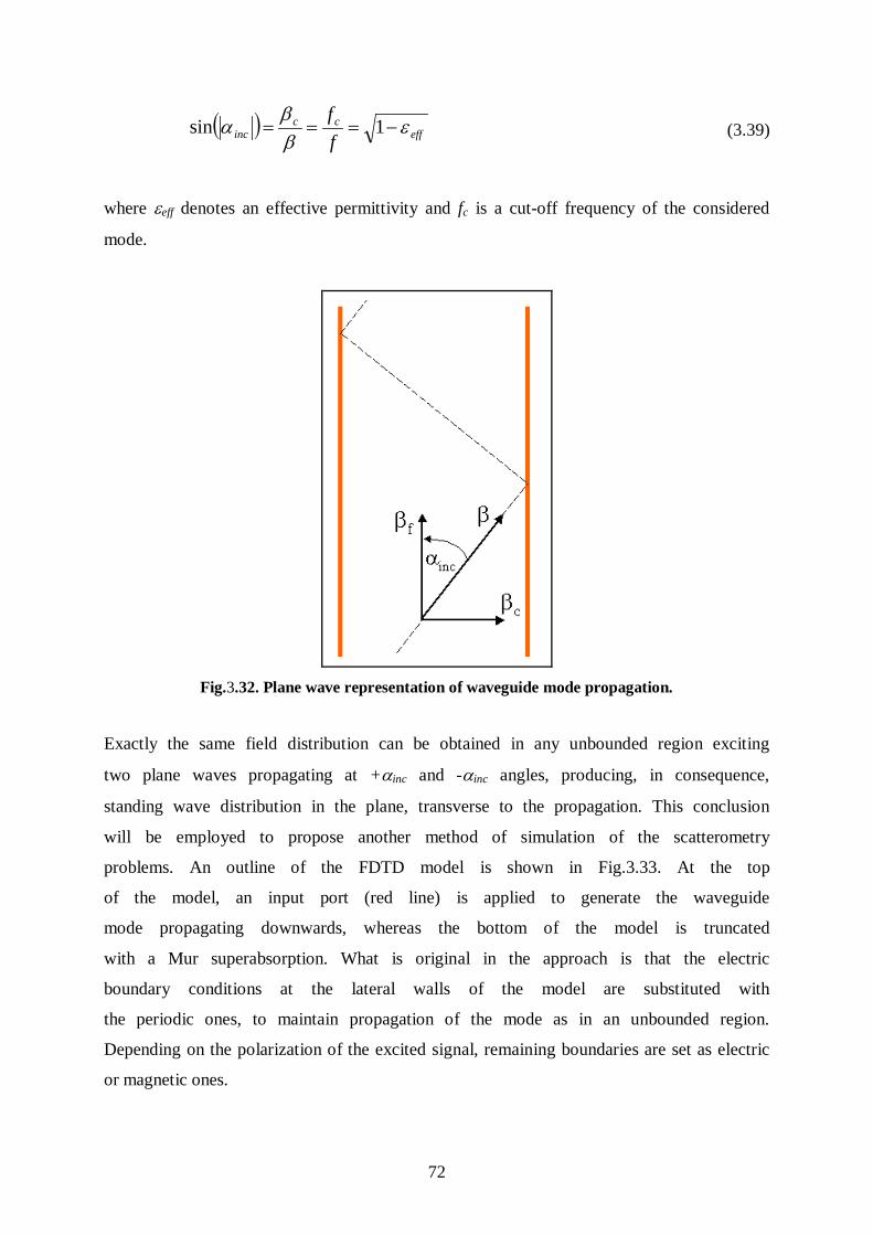
72
( ) effcc
inc ff
εββ
α −=== 1sin (3.39)
where εeff denotes an effective permittivity and fc is a cut-off frequency of the considered
mode.
Fig.3.32. Plane wave representation of waveguide mode propagation.
Exactly the same field distribution can be obtained in any unbounded region exciting
two plane waves propagating at +αinc and -αinc angles, producing, in consequence,
standing wave distribution in the plane, transverse to the propagation. This conclusion
will be employed to propose another method of simulation of the scatterometry
problems. An outline of the FDTD model is shown in Fig.3.33. At the top
of the model, an input port (red line) is applied to generate the waveguide
mode propagating downwards, whereas the bottom of the model is truncated
with a Mur superabsorption. What is original in the approach is that the electric
boundary conditions at the lateral walls of the model are substituted with
the periodic ones, to maintain propagation of the mode as in an unbounded region.
Depending on the polarization of the excited signal, remaining boundaries are set as electric
or magnetic ones.

73
Fig.3.33. Waveguide model with PBC for the scattering of periodic structures.
According to Eq.3.26, an appropriate Floquet phase shift per period is set at the periodic
boundary conditions to maintain undisturbed propagation of the mode related to the incident
angle (see Eq.3.39). Calculation of the mode template at the input port cross-section is
performed using the advantage of the V2D FDTD solver [48], with the following propagation
constant, understood as a simulation parameter (more details can be found in Section 3.4.2):
efff cf
επ
β 00
2= (3.40)
A scattering matrix with a reflection coefficient (S11) is calculated below the input port at a
reference plane (a blue dashed line), in the same manner as for nonperiodic waveguide
templates [7],[62]. If there is any scattering object inside the model, at least two specularly
reflected rays are expected since the input port generates two plane waves at ±αinc.
The proposed mode template method is relatively simple and versatile in its applicability. In
QuickWave-3D software package [48] used by the author of this thesis, the procedure is
executed automatically with no need of any user control. A user just needs to define a
frequency and an effective permittivity associated with a particular incident angle. However,
there is a fundamental limitation. The method proposed in this Section is useless when higher
diffraction orders are not evanescent. It stems from the principal assumption which must be

74
satisfied to calculate a scattering matrix. The assumption is that waveguide modes are
orthogonal with each other in the following sense:
( ) ( )∫∫ =× ⊥⊥S
ji dxdyyxhyxe 0,, (3.41)
where e⊥i (x,y) and h⊥j (x,y) are orthonormal distributions of transverse electric and magnetic
components of the ith and jth modes (i≠j), respectively.
It may be easily proven that the above relation is not satisfied for higher
diffraction orders, when the periodic boundary conditions are imposed instead
of electric or magnetic ones (see Fig.3.33). It follows from the fact that
orthogonality of waveguide modes is satisfied if strict (electric/magnetic)
boundary conditions are imposed. Thus, the field distribution at a waveguide
cross-section can be expressed as a sine/cosine series that, by definition, sets
an orthogonal basis. On the contrary, periodic boundary conditions allow
each mode to propagate with an arbitrary phase shift along the periodicity axis.
Thus, if a higher diffraction order appears, it may be arbitrarily shifted
with respect to a fundamental mode loosing orthogonality needed to separate them.
Let us check the correctness of the aforementioned method by considering
an empty model L = 10 mm wide, located between PBCs. The aim is to excite
a TE polarized standing wave at f = 15 GHz, with the magnitude of an incident
angle equal to |αinc| = 300. Thus, according to Eq.3.23, higher diffraction
orders are not supposed to appear. Eq.3.39 allows evaluation of the effective
permittivity of the searched mode, and it amounts to εeff = 0.75. Next,
according to Eq.3.26, the Floquet phase shift per period is ψx = π/2 rad. The mode
template is computed with the V2D FDTD algorithm, with the longitudinal
phase constant equal to βf = 0.272 rad/mm (see Eq.3.40). Afterwards, the calculated
mode template is coupled with the whole model shown in Fig.3.33, driving it with
the pulse of a spectrum deliberately wider than usually necessary to visualize
some properties of the method.

75
Fig.3.34. Reflection coefficient |S11| obtained in a periodic empty model
excited with a TE mode template (L=10mm, fc=7.5GHz, f=15GHz, εeff=0.75).
Table 3.4. Values taken from the reflection coefficient shown in Fig.3.34.
f [GHz] |S11| [dB]
Cut-off frequency of the fundamental mode 7.5 -2.6
Matching frequency of the fundamental mode 15 -61.3
Cut-off frequency of the second mode 22.58 -17.9
Fig.3.34 shows the magnitude of the reflection coefficient |S11| extracted at the reference
plane. The marker values are shown in Table 3.4. It can be noticed that, indeed, the reflection
is negligibly small at f = 15 GHz (matched frequency), which proves that there is no obstacle
placed inside the model which would diffract the incident wave. Nevertheless, when the
frequency deviates from the matched value, the magnitude of the reflection coefficient |S11|
increases, and at least three reasons may be specified for that. First of all, the Mur
superabsorption applied at the bottom of the model is matched to a plane wave incident at
|αinc| = 300 but, for the specified mode template (fixed effective permittivity), this angle varies
with frequency (compare Eq.3.40). Secondly, as the frequency decreases, the considered
mode is getting closer to its cut-off, which may be directly derived from Eq.3.39. In that case,
it is equal to fc = 7.5 GHz, which is consistent with the plot shown in Fig.3.34 since |S11|
reaches its global maximum exactly there. Last but not least, as it has already been mentioned,

76
the method is only applicable to the investigation of specular reflection. Substituting Eq.3.39
to Eq.3.23 and equating the latter to unity, the following relation is obtained:
( ) ( ) 1sinsin 1 =−=−=−=ff
fLc
ff
LLcc
incλαλα (3.42)
The above formula enables detection of the cut-off frequency of the 1st diffraction order. The
calculated frequency fc1 = 22.5 GHz is in a good agreement with the reflection coefficient |S11|
that, indeed, reaches the local maximum of about -18dB there.
Fig.3.35. FDTD model of a dielectric grating.
Since validity of the method has just been confirmed in an empty air region, let us go further
and check how it will work if an obstacle is placed inside the model. Fig.3.35 shows the
scenario consisting of one period of teflon dielectric grating (εr = 2.2). The height of the line
is 20mm, whereas the line to space ratio is exactly L/S = 0.5. The size of the FDTD cell
applied during the simulation is a = 0.5 mm, satisfying dispersive requirements of the FDTD
algorithm with a large surplus since about 27 cells/λ in the dielectric region are applied.
Fig.3.36 shows the plot of |S11| around the frequency of interest, and it can be observed that

77
the reflection coefficient is equal to |S11| = 0.097740 at f = 15 GHz. Simulation speed reaches
13700 iter/sec, providing a convergent result after just about 10 ms7
.
Fig.3.36. Reflection coefficient |S11| obtained for a dielectric grating (εr=2.2)
excited with a TE mode template (L=10mm, fc=7.5GHz, f=15GHz, εeff=0.75).
Fig.3.37. Normalized scattering pattern for the dielectric grating shown in Fig.3.35 illuminated
with a TE polarized plane wave at αinc = 300 (f = 15GHz).
7 Intel Core™2 Duo CPU 3.00GHz, 4094MB RAM, 64-bit Windows Vista Business.

78
Fig.3.38. Reflection coefficient |S11| obtained for a dielectric grating (εr=2.2)
excited with a TM mode template (L=10mm, fc=7.5GHz, f=15GHz, εeff=0.75).
Fig.3.39. Normalized angular scattering pattern for the dielectric grating shown in Fig.3.35
illuminated with a TM polarized plane wave at αinc = 300 (f = 15GHz).
Now, let us assess the reliability of the proposed waveguide periodic approach.
A normalized angular scattering pattern has been calculated for the same dielectric
grating, but this time illuminated with a purely traveling plane wave (see Fig.3.21).

79
As shown in Fig.3.37, the reflection coefficient is equal to 0.097628, so
the discrepancy between the results obtained using both FDTD models reaches
about 0.01%. This time a simulation is slightly faster, reaching 14000 iter/sec,
with approximately the same computation time. However, the NTF solution
stabilizes at the second significant digit, whereas |S11| provides five stable
significant digits. Apparently, it makes the mode template method more reliable
for the modeling of electrically short scenarios.
To make the analysis complete, let us consider the same problem but with
a TM polarized wave. Fig.3.38,39 depict the reflection coefficient |S11| and
the angular scattering pattern, respectively. Obtained results differ at the level
of about 0.02%, however, like for the TE polarization, only two significant digits
are stable in the ASP and five in |S11|. Nevertheless, extension of the model
to two periods of the grating would alleviate NTF problem at the cost of doubling
computational effort.
Now, let us modify the proposed model by changing periodic boundary conditions
to perfect electric conductor (see Fig.3.40). First of all, it enables the application
of the classic FDTD algorithm with one simulation grid, instead of the
CL-FDTD one with two grids, reducing the computational effort at least twice.
However, at the same time the mode template flexibility is restricted. Due to the
PEC imposed at the sidewalls of the model, only the modes that satisfy the following
discrete set of phase shifts can be excited:
πβ mLxx = (3.43)
Hence, the following set of incident angles can be obtained:
( )x
xminc L
mβ
πββ
α ==sin (3.44)
where m = 1, 2, 3, …

80
The above formula leads to the major property of the proposed model. The length of the
whole model has to be an integer multiple of the fundamental period of the modeled structure
Lx = n Lxp. Thus, in order to obtain a particular incidence angle αinc for a specified frequency,
the value of the parameter m has to be selected in a way which ensures that the chosen
incident angle mincα is close enough to the intended one:
( )xp
minc Lnm
βπα =sin (3.45)
Fig.3.40. Waveguide model with PEC sides for the scattering of periodic structures.
There is a visible tendency for the step between consecutive incident angles mincα to decrease
with the increasing length of the structure (n >> 1). Hence, in general, a better accuracy can
be obtained if the model is longer. However, as it will be shown, this requirement may be
alleviated under some conditions.
Let us consider incidence of a plane wave on the dielectric coated PEC cross-shaped grating
already introduced in this Chapter (see Fig.3.25). The analysis is confined to one frequency
point, i.e. d/λ0 = 0.125. First, let us check how precisely an incidence angle can be selected.
Eq.3.45 indicates that the precision of the angle selection rises with the increasing length of
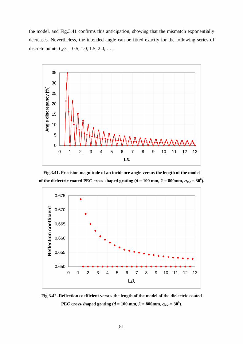
81
the model, and Fig.3.41 confirms this anticipation, showing that the mismatch exponentially
decreases. Nevertheless, the intended angle can be fitted exactly for the following series of
discrete points Lx/λ = 0.5, 1.0, 1.5, 2.0, … .
0
5
10
15
20
25
30
35
0 1 2 3 4 5 6 7 8 9 10 11 12 13
L/λ
Ang
le d
iscr
epan
cy [%
]
Fig.3.41. Precision magnitude of an incidence angle versus the length of the model
of the dielectric coated PEC cross-shaped grating (d = 100 mm, λ = 800mm, αinc = 300).
0.650
0.655
0.660
0.665
0.670
0.675
0 1 2 3 4 5 6 7 8 9 10 11 12 13
L/λ
Ref
lect
ion
coef
ficie
nt
Fig.3.42. Reflection coefficient versus the length of the model of the dielectric coated
PEC cross-shaped grating (d = 100 mm, λ = 800mm, αinc = 300).

82
Next, simulations have been performed for varying model length to show that the mismatch of
an illumination angle has a major contribution to the accuracy of the obtained reflection
coefficient. Fig.3.42 shows that the model does not have to be very long to get the accurate
result provided that the intended incidence angle is exactly fitted. Reflection coefficients
obtained for the unmatched points exponentially converge to the accurate value.
Another essential feature of the waveguide method with PEC lateral boundaries is the
possibility to evaluate higher diffraction orders. Contrary to the already introduced waveguide
model with PBCs, where waveguide-like modes are considered (see Fig.3.33), the PEC
version of the model excites strictly a waveguide mode, which is orthogonal to the other
modes. Moreover, if the fundamental mode is properly adjusted to the corresponding
incidence angle (see Eq.3.45), the potential higher diffraction orders will also satisfy electric
boundary conditions at the waveguide port. Therefore, if another port matched to the higher
order mode is defined in the same place as the input port, it is possible to monitor the amount
of power reflected at the considered higher diffraction order.
To exemplify the method, let us go back to the structure shown in Fig.3.25 illuminated in the
xy-plane at an angle of αinc = 300. It will be investigated on one frequency for d/λ0 = 0.883 (f
= 2.65 GHz). According to Eq.3.23, the 1st diffraction order can be expected at α1 = 39.20,
which corresponds to (φ, θ) = (129.20, 900) in spherical coordinates8
. The model with 17
fundamental periods of grating is defined since such a length of the model enables to keep a
good matching of two mode templates which correspond to the 0th and the 1st diffraction
orders. Following Eq.3.39, the effective permittivity of the fundamental mode is equal to εeff =
0.750366, which is equivalent to the incidence angle of αinc = 29.980. As regards another
mode, it has the effective permittivity equal to εeff = 0.599477, corresponding to α1 = 39.260.
Thus, intended angles are matched with the accuracy better than 0.1%.
The structure is excited with a short pulse with the spectrum within 2.5 – 3.0 GHz, providing
the following scattering parameters: |S11|2 = 0.748 and |S21|2 = 0.156. The first value
corresponds to the power reflection coefficient of the 0th order, whereas the second value is
understood as the power transmission coefficient from the 0th order mode to the 1st one.
However, to assess the reliability of the obtained solution, the simulation of the same scenario
8 See Appendix 3.

83
will be run in the already studied plane wave excitation model (see Fig.3.21). Fig.3.43
presents the obtained scattering pattern in a quadratic (power) scaling and, indeed, the ray of
the 1st diffraction order can be observed. The comparison of the results obtained with both
methods, shown in Table 3.5, indicates that the discrepancy is about 0.4% and 1.1% for the 0th
and the 1st order, respectively, with approximately the same computation time.
Fig.3.43. Angular scattering pattern (power scaling) for the dielectric coated
PEC cross-shaped grating (d = 100 mm, αinc = 300, f = 2.65GHz) obtained in a 17 periods model.
Table 3.5. Values taken from the angular scattering patterns shown in Fig.3.43.
|S11|2 |S21|2 RP0 (600/3000) RP1 (1290/3000)
0.748 0.156 0.752 0.145
The main advantage of the approach with PEC boundary conditions is 50% smaller
computational effort as compared to the model with PBCs imposed. However, the major
disadvantage of the first method is the necessity to match precisely the waveguide mode to the
intended incidence angle, which can impose definition of a longer FDTD model.
In the aforementioned waveguide approach, a periodic structure has been extended to the
whole length of the model. In principle, it refers to the case of an infinite spot over an infinite
structure (see Section 4.5). It should be emphasized, however, that the waveguide approach

84
might be also applicable to the investigation of an infinite spot over a finite structure (see
Fig.3.44). Practically, it refers to so-called isolated targets, composed of periodic structures
separated from each other by the same distance. In such a scenario, a periodic structure is
shorter than the whole waveguide model, which may be useful when investigating the impact
of the diffraction on edges of the targets on the angular scattering pattern. However, since the
concept of the FDTD model does not change at all in this case, a thorough investigation of
this issue will be omitted here.
a) b)
Fig.3.44. Waveguide model with PEC sidewalls for the infinite spot size scattering
of infinite (a) / finite (b) periodic structure.
So far, a few methods useful to the modeling of a plane wave scattering from periodic
structures have been considered. First, an approximate approach was studied, which allows
reducing the FDTD model to one or just a few fundamental periods of the structure,
depending on the required computational precision. Two types of simulation models have
been investigated in that case: a plane wave source and a waveguide port with periodic
boundary conditions. Next, it was proposed to modify a waveguide approach exchanging
PBCs with PEC to reduce computational effort, and to extend applicability of the model to
higher diffraction orders. The summary of the advantages and limitations of these methods is
presented in Table 3.6. The results prove the first statement of the thesis posed in Chapter 1.
In the next Section, the attention will be focused on a Gaussian beam illumination of a
periodic structure.

85
Table 3.6. Pros and cons of the methods introduced in Section 3.5.1.
Method Pros Cons
PLW & NTF
&PBC
1. A possibility to reduce
an FDTD model to one or few
periods of a structure.
2. Simulation possible for
an arbitrary angle of incidence
and an arbitrary polarization.
3. Possible detection of
higher diffraction orders.
1. Accuracy only at a single
matching frequency.
2. Doubled memory
occupation (two FDTD grids).
WG port & PBC
1. A robust technique taking
advantage of well-established
modal templates excitation
and extraction.
1. Accuracy only at a single
matching frequency.
2. Doubled memory
occupation (two FDTD grids).
3. Accurate only for
specular (mirror-like)
reflection.
WG port & PEC
1. The most robust technique
among those on the list (due to
rigid boundary conditions).
2. Possible analysis of
higher diffraction orders.
3. A single FDTD grid.
1. Accuracy strongly dependent
on waveguide mode matching to
the corresponding angle of
incidence.
3.5.2 Gaussian Beam Illumination of Periodic Structures
In principle, the plane wave excitation considered so far is a simplified formalism used to
approximate an electromagnetic wave propagating in a particular direction far from a
radiation source. Such a specific approximation is often sufficient for the modeling of
practical problems, although, in fact, an EM wave never maintains a plane wavefront when
propagating in a linear medium. On the contrary, the wavefront always converges or diverges
when receding from a source. The most popular approximation of such a case is known as a
Gaussian beam.

86
Fig.3.45. Shape of a Gaussian beam in a focal plane (y = 0).
The following formulae describe 3D and 2D Gaussian beams propagating along the y-axis
[63], respectively:
( ) ( ) ( )
−
++−−=
020
2
2
2
20
0 tan2
expyya
yyryyj
ywr
yww
EE ββ (3.46)
( ) ( ) ( )
−
++−−=
020
2
2
2
20
0 tan21
2exp
yya
yyxyyj
ywx
yww
EE ββ (3.47)
where
22 zxr +=
( )20
2
0 1yywyw += (3.48)
2
20
0w
yβ
= (3.49)
and w0 stands for the beam’s spot radius understood as the distance from the Gaussian beam
axis in the focal plane where the amplitude decreases by 1/e (see Fig.3.45).

87
Fig.3.46. Scheme of the FDTD model for a Gaussian beam obliquely incident
on the structure periodic along the x-axis.
In this thesis, without loss of generality, the attention will be focused on the 2D FDTD model
of a Gaussian beam illumination of a periodic structure, taking advantage of the classic FDTD
algorithm. Fig.3.46 shows the FDTD model which will be applied hereafter. In principle, it is
very similar to the one shown in Fig.3.21. However, this time a plane wave wall (PLW) is
substituted with a Gaussian beam wall (GBW). In principle, operation of a GBW source is
similar to a PLW one in a sense that it divides the considered volume into total and scattered
field regions (compare Fig.3.21). The only difference is in the shape of the beam. In this
particular scenario shown in Fig.3.46, GBW excites a Gaussian beam propagating
downwards, whereas the area above is filled only with scattered field (if such is generated).
Moreover, periodic boundary conditions, originally placed at the sidewalls, are replaced with
a Mur superabsorption, truncating the volume of the FDTD model. The model is long enough,
as compared to the beam’s spot radius, to avoid spurious diffraction of the EM field from the
absorbing sidewalls. The definition of the TE/TM polarization, which will be used below, can
be found in Fig.3.19.
Fig.3.47 shows an example of a TE polarized 2D Gaussian beam propagating obliquely in the
empty air model and centered in the middle. The beam is incident at λinc = 250 and driven with
88
a sinusoidal excitation at λ = 0.5µm (see Fig.3.20). It will be applied to illuminate the periodic
structure placed below the NTF plane.
Fig.3.47. Snapshots of the electric field (left) and the envelope (right) for a TE polarized
2D Gaussian beam incident in the xy-plane (λ = 0.5µm, w0 = 1µm, AOI = 250).
Let us consider the poly-to-active stack already shown in Fig.3.29. The initial results of the
author’s studies of this issue were published in [64]. Fig.3.30 depicts the spectrum of the
reflection coefficient computed with the CL-FDTD algorithm. First, analysis of the scenario
excited with a Gaussian beam of w0 = 20µm spot diameter will be executed and the obtained
reflection coefficient will be compared to the one shown in Fig.3.30. Fig.3.48 shows the
computational results of both methods and a good agreement can be noticed. It confirms that a
plane wave illumination of an infinite structure can be a good method to overcome the
computational limitations of the real scattering problem with a spatially finite illumination
spot.
Once the agreement between infinite and finite approaches has been confirmed
for a large beam diameter, it will be assessed how the finite solution diverges when
the spot is getting smaller. For this purpose, let us perform several simulations
to observe a deviation of the relevant reflection coefficient with diminishing spot size.
It should be emphasized, however, that the sensitivity of the reflection coefficient
on the spot size is scenario-dependent so the conclusions derived below cannot be understood
as general.

89
Fig.3.48. Reflection coefficient for a TE polarized 2D Gaussian beam
incident at 250 on the target shown in Fig.3.29.
Fig.3.49,50 show the absolute deviation of TE and TM reflection coefficients as a function of
diminishing spot size. The following formula has been applied to calculate the absolute
deviation:
[ ] ( )refkk RRR −=∆ 100% (3.50)
where Rk stands for a considered reflection coefficient Rss (Rpp) and Rref denotes the reference
value of Rss (Rpp) obtained for the largest spot size.
The largest spot covers about 62 pitches of the considered poly-to-active stack,
whereas the smallest one covers only two pitches. It can be noticed that sensitivity
to the spot size is of the order of 0.3% and 0.1% for the TE and
TM polarizations, respectively, down to a 2-3 micron spot size (6-10 pitches). It can
also be noticed that the TM polarization is less sensitive to the spot size changes.
However, below the level of 2-3 microns we observe rapid changes of the reflection
coefficients.
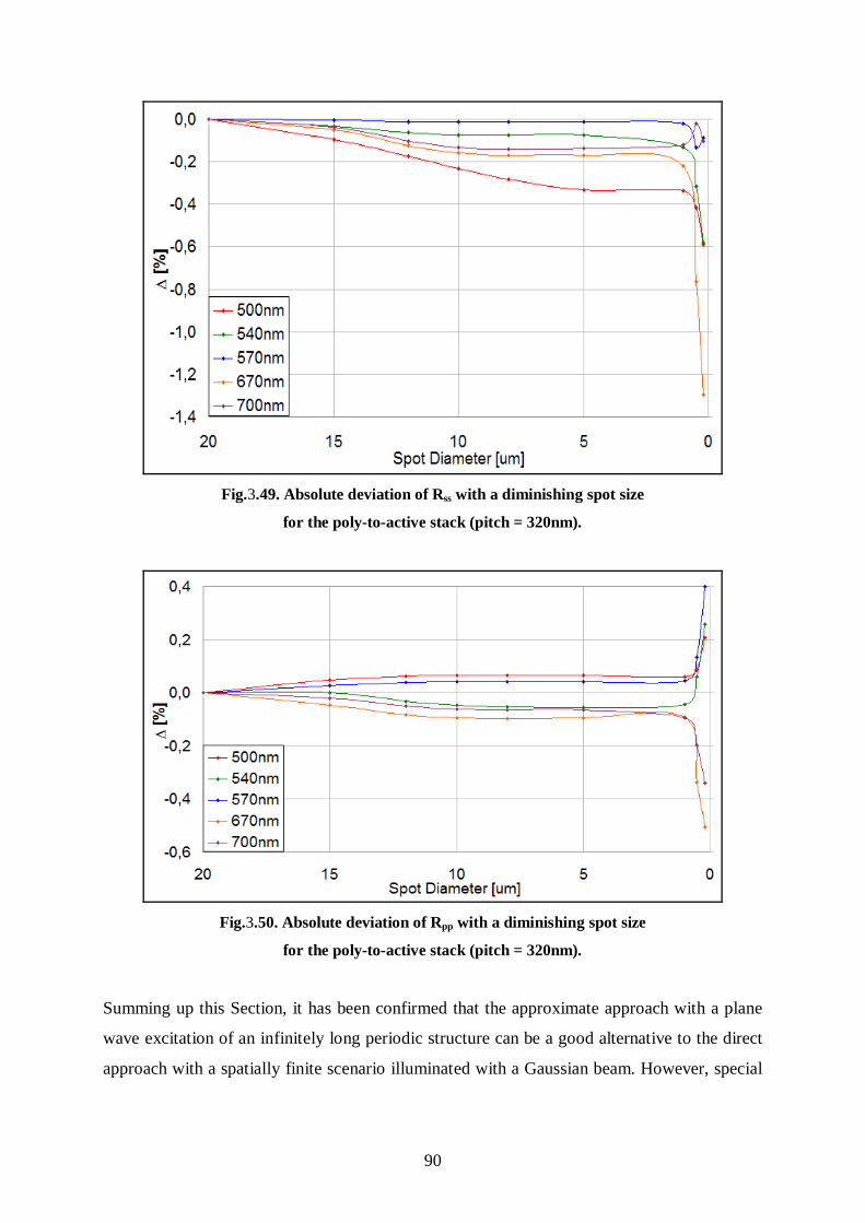
90
Fig.3.49. Absolute deviation of Rss with a diminishing spot size
for the poly-to-active stack (pitch = 320nm).
Fig.3.50. Absolute deviation of Rpp with a diminishing spot size
for the poly-to-active stack (pitch = 320nm).
Summing up this Section, it has been confirmed that the approximate approach with a plane
wave excitation of an infinitely long periodic structure can be a good alternative to the direct
approach with a spatially finite scenario illuminated with a Gaussian beam. However, special
91
care as regards to the accuracy of the approximation must be taken if a spot is relatively small
as compared to the number of illuminated periods.
3.6 Summary
The application of the partially analytical FDTD method dedicated to the modeling of
electromagnetic wave scattering from periodic structures has been studied in this Chapter. A
thorough insight into the procedure of looping periodic boundary conditions in the CL-FDTD
algorithm extended by the author to 2D and 3D periodicity has been given. The author has
also applied 1D and 2D PBCs in the V2D FDTD method. It has been shown that the
implemented features allow simulating both eigenvalue and deterministic periodic problems.
Special attention has been focused on the applicability to the modeling of plane wave
scattering from infinite periodic structures. For that purpose, two types of modeling scenarios
have been introduced and cross-compared, taking into account many modeling criteria, such
as polarization, beam shape, diffraction orders and the size of the model. The first scenario
takes advantage of a plane wave wall and a near-to-far transformation, which allow
simulation and accurate extraction of the specular and higher diffraction orders. The second
modeling scenario is based on the waveguide approach. In the first version of this approach,
the periodic boundary conditions have been applied. It has been shown that the method is
dedicated to the modeling of specular reflection only. However, by substituting periodic
boundary conditions with a perfect electric conductor, it is possible to extend the applicability
of the waveguide method to the higher diffraction orders, but at the expense of a mismatch of
the incident angle. Finally, the last Section of this Chapter has been focused on a Gaussian
beam illumination of a periodic structure as the most realistic case. The study presented in this
Chapter fully proves the first statement of the thesis, formulated in Chapter 1.
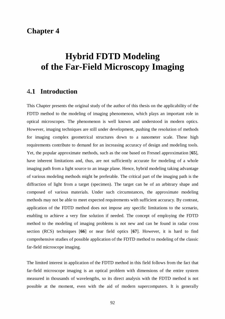
92
Chapter 4
Hybrid FDTD Modeling of the Far-Field Microscopy Imaging
4.1 Introduction
This Chapter presents the original study of the author of this thesis on the applicability of the
FDTD method to the modeling of imaging phenomenon, which plays an important role in
optical microscopes. The phenomenon is well known and understood in modern optics.
However, imaging techniques are still under development, pushing the resolution of methods
for imaging complex geometrical structures down to a nanometer scale. These high
requirements contribute to demand for an increasing accuracy of design and modeling tools.
Yet, the popular approximate methods, such as the one based on Fresnel approximation [65],
have inherent limitations and, thus, are not sufficiently accurate for modeling of a whole
imaging path from a light source to an image plane. Hence, hybrid modeling taking advantage
of various modeling methods might be preferable. The critical part of the imaging path is the
diffraction of light from a target (specimen). The target can be of an arbitrary shape and
composed of various materials. Under such circumstances, the approximate modeling
methods may not be able to meet expected requirements with sufficient accuracy. By contrast,
application of the FDTD method does not impose any specific limitations to the scenario,
enabling to achieve a very fine solution if needed. The concept of employing the FDTD
method to the modeling of imaging problems is not new and can be found in radar cross
section (RCS) techniques [66] or near field optics [67]. However, it is hard to find
comprehensive studies of possible application of the FDTD method to modeling of the classic
far-field microscope imaging.
The limited interest in application of the FDTD method in this field follows from the fact that
far-field microscope imaging is an optical problem with dimensions of the entire system
measured in thousands of wavelengths, so its direct analysis with the FDTD method is not
possible at the moment, even with the aid of modern supercomputers. It is generally

93
recognized that present computer systems allow 3D analysis of objects having linear
dimensions not bigger than a few dozens of wavelengths. This is the main reason behind its
narrow range of application in optics where the electrical size of objects is typically much
bigger. However, the FDTD method as a full-wave approach has several advantages
prompting us to apply it in a selected part of computational domain and to combine it with
other methods typical for optics. Therefore, this Chapter addresses the issue of the potential
application of the FDTD method coupled with a particular approximate optical approach to
enhance capabilities of the overall algorithm of the far-field microscope imaging. Initial
results of the author’s work presented below have been published in [68],[69],[70].
The main goal of this study is to define an algorithm that takes advantage of the FDTD
method in modeling of an imaging phenomenon exploited in the far-field microscope systems.
These imaging methods have various practical applications, including the quality control of
masks and reticles in the lithography process of integrated circuits or 3D imaging of
biological tissues, to name just a few. First, a theoretical background - essential in the
understanding of the chosen modeling method - will be provided. Then, a brief survey of the
hybrid algorithms that take advantage of the FDTD method in the modeling of far-field
optical imaging problems will be presented. Subsequently, wide-field microscopy will be
considered as a basic concept exploited in optical microscopes [71]. Eventually, the study will
be extended to confocal imaging systems [71] dedicated to the analysis of 3D geometry of a
thick target (specimen). Since the main scope of this Chapter is strictly related to optical
problems, notation usually applied in that field is used hereafter. In particular, the symbol i is
used instead of j to denote a complex number. Moreover, it is assumed that a monochromatic
plane wave has the following notation:
tirki eeUU ω−= 0 (4.1)
The difference as compared to the notation common in electronics and used in the previous
Chapters of this thesis lies in the opposite sign of the argument in the exponent.

94
4.2 Theoretical Background
A brief historical review of how the formalism explaining a diffraction phenomenon was
developed will precede the study of the optical imaging, as it plays a key role in the concept
of imaging theory. Essentially, although there is a variety of imaging systems depending on
the particular technology applied, a final image is always obtained by an appropriate
processing of light diffracted from or transmitted through a target (specimen).
In 1678, a Dutch physicist, Christiaan Huygens, formulated the main concept that became a
starting point for the further study in this field. He stated that each point of the advancing
wavefront is a source of a new spherical radiation, and all the secondary waves reconstruct the
wavefront. Subsequently, this concept had been independently developed by Thomas Young
(1804) and Augustin-Jean Fresnel (1818). However, Gustav Kirchhoff (1882) was the first
who formulated an explicit solution of the wave equation with well-defined boundary
conditions [72].
Fig.4.1. Point source radiation through the aperture.
Let us assume that a point source of electromagnetic radiation illuminates an air hole in an
unbounded metal layer as shown in Fig.4.1. For the purpose of this study, the problem is
reduced to the scalar one, neglecting the issue of source polarization. According to the

95
Fresnel-Kirchhoff diffraction principle, the field behind the wall is given by the following
formula:
( ) ( ) ( )[ ] ( ) ( )∫∫
−+
=S
dsrnrnrr
rrkiiPUPU
2,ˆcos,ˆcosexp 2101
0121
012120
λ (4.2)
Subsequently, assuming that the radiation source U(P2) is far from the air hole (r21 >> λ), the
Rayleigh-Sommerfeld approach leads to a simplified integral with the integration over the air
hole surface:
( ) ( ) ( ) ( )∫∫=S
dsrnr
rkiPUi
PU 0101
0110 ,ˆcosexp1
λ (4.3)
A brief look upon this equation allows us to recognize the Huygens principle since the field is
integrated over each point within the air hole, as if it were a source of a spherical wave
(modified by the cosine directional coefficient).
Subsequently, applying a paraxial Fresnel approximation (∠(n,r01) ~ 00), Eq.4.3 can be
simplified to the following one:
( ) ( ) ( ) ( )[ ]∫∫ ′′′′=
′−+′−
S
yyxxz
ikzki
ydxdeyxUzi
eyxU22
2,,λ (4.4)
It can be noticed (see Eq.4.4) that the field at the observation point U(x,y) may be understood
as a 2D convolution of the source field distribution U(x’,y’) and the impulse response of a free
space region given by:
( ) ( )22
2,yx
zikzki
ezi
eyxh+
=λ (4.5)

96
Appropriate rearrangement of Eq.4.4 leads to the following expression:
( ) ( ) ( ) ( )∫∫ ′′′′=
′+′−′+′+
S
yz
yxz
xiyxz
ikyxz
ikzki
ydxdeeyxUezi
eyxU λλπ
λ
222
2222
,, (4.6)
where one can recognize Fourier transform to an angular domain:
( ) ( ) ( ) ( )
′′ℑ=
′+′+ 2222
22 ,,yx
zikyx
zikzki
eyxUezi
eyxUλ (4.7)
with the following definition of angular frequencies:
zyfz
xf yx λλ == ; (4.8)
Let us introduce the last approximation, known as Fraunhofer (or far field) approximation,
assuming that the source is electrically small as compared to the distance to the observation
point. Thus, the equation - well known in the antenna theory [73] - is obtained [71]:
( ) ( ) ( )∫∫ ′′′′=
′+′−+
S
yz
yxz
xiyxz
ikzki
ydxdeyxUezi
eyxU λλπ
λ
22 ,,
22
(4.9)
The above expression evidently depicts that the free space between the electromagnetic
source and the observation point located in Fraunhofer region performs Fourier transform to
the angular domain of the source field spatial distribution.
Each of the approximations outlined above reduces the computational effort when
calculating field at the observation point. The Fresnel formula (see Eq.4.4)
always converges to the Fraunhofer one (see Eq.4.9) with an increasing distance.
Typically, in modeling of the far-field microscope imaging the Fresnel approach

97
is employed to avoid the risk of potential inaccuracy of the Fraunhofer approximation,
although it needs to be mentioned that such an approach requires higher computer effort.
The Fourier transform allows substitution of a time consuming convolution appearing in the
Fresnel formula (see Eq.4.4), with a much simpler multiplication in a Fourier domain:
( ) ( ) ( )yxoyxyxi ffUffhffU ,,, = (4.10)
where [71]:
( ) ( )2225.0, yx ffdkidkiyx eeffh +−= λ
(4.11)
and the subscripts o and i denote the image and object planes, respectively.
Regarding spherical lenses, the simplest approximation is a perfectly thin spherical lens
described by the following phase transfer function [71]:
( )( )22
2,yx
fki
L eyxt+−
= (4.12)
where f stands for the lens focal length.
Field distribution behind the lens is the product of the field in front of the lens and the lens
transfer function:
( ) ( ) ( )yxUyxtyxU L ,,, 12 = (4.13)
It indicates that the Fourier transform is not preferable in this area since
the spatial multiplication given by Eq.4.13 would have been changed to
time consuming convolution in a Fourier (angular) domain. Finally, field distribution
behind the lens U2(x,y) can be processed to an image plane applying impulse
response of an open air region between the lens and the image plane, in a similar way as in
Eq.4.10.

98
To summarize, the part of diffraction theory important from the point of view of
electromagnetic modeling of the far-field microscope imaging investigated hereafter has been
recalled. The next Section is focused on applicability of the FDTD method to EM modeling of
a classic wide-field microscope.
4.3 State-of-the-art
Due to the reason mentioned in the previous Section, the literature concerning applicability of
the FDTD method to the modeling of the far-field imaging problems is very limited. One can
find a lot of research done in the field of breast cancer detection [74], but it works with a
different approach to the imaging concept (not utilizing focusing elements like lenses). In
2004 Hollmann et al. published a paper [75] about the hybrid FDTD-Fresnel imaging of living
tissues (embryo). The authors applied the FDTD method in a close vicinity of the target, in
order to expose it to plane wave illumination and to obtain scattered fields in the whole
surrounding volume. These volume fields were further processed with 3D Green’s function to
get the fields at the lens plane. The rest of the imaging path was modeled with the aid of the
Fresnel approximation. In principle, this is a slightly different approach from the one which is
going to be developed in this Chapter since in real microscopes the target is never totally
exposed to a scanning beam, but the beam is spatially restricted to the focal spot of a
particular dimension.
Another notification about the hybrid FDTD-Fresnel modeling can be found on the website of
the PlanetQuest project, led by Jet Propulsion Laboratory [76], where the FDTD method
together with the so-called Fresnel propagator are applied to process measurement results of
distant stars and planets with a real confocal optical system. However, there are no details
provided about the modeling conditions.
The last paper that is going to be addressed is [77]. It refers to EM modeling of the confocal
3D imaging of subwavelength features. The authors proposed the FDTD model with a
Gaussian beam illumination for the confocal characterization of 2D nanovoids fabricated
inside a polymer volume. The scheme of the FDTD model looks similar to the one proposed
by the author in Section 4.5, but [77] lacks comprehensive explanation how the final image is
processed. The authors focused on application rather than on detailed description of the
modeling issue.

99
4.4 Hybrid FDTD Modeling of the Wide-Field Microscopy
Historically, the wide-field microscopy was the first imaging concept applicable
in the microscopes built of optical lenses. Although modern imaging tools are
much more sophisticated, with specialized techniques applied to push the resolution
down to the physical limits of the particular technology, the basic idea has remained
the same. Therefore, without loss of generality of further conclusions, the study
presented hereafter will be confined to a simple imaging scenario composed of
one spherical lens, in order to concentrate only on the hybrid modeling
of the imaging phenomenon. The goal is to assess whether the FDTD method
can enhance capabilities of the modeling algorithms used in optics. Let us first
introduce the investigated scenario and present its short theoretical description.
4.4.3 Introduction to Wide-Field Microscopy
Fig.4.2 shows a lens-imaging scenario which will be studied in this Section. There are
various types of wide-field microscopy systems, such as transmitted, reflected, etc. This
study will be concentrated on the reflected light microscopy. Let us assume a perfectly
thin lens approximation [71] to suppress an aberration issue. According to geometrical optics,
the thin lens formula relates the object distance zo with the image distance zi in the following
manner:
io zzf111
+= (4.14)
where f stands for the focal length of a lens.
The ratio between image and object distances determines the magnification factor M
of a single lens system. The obtained image is inversed with respect to the object.
However, although geometrical optics allows some estimation of the object
plane and magnification, it does not quantitatively explain how the image is constructed.
This is a role of the diffraction theory, already pointed out in Section 4.2.

100
Fig.4.2. Single lens imaging scenario.
The target located at the object plane is illuminated with light focused by the objective lens.
The major parameter of the objective lens is the numerical aperture (NA) associated with the
half-angle θ of the focused light cone:
( )θsinnNA = (4.15)
where n stands for the refraction index of the medium between the objective lens and the
target.
It should be emphasized that NA of the illumination beam can differ from the NA of the beam
collected by the lens after diffraction from the target. The numerical aperture of the
illumination beam determines the observation area, whereas NA of the collected beam implies
the resolution limit. However, in many cases both NAs are the same. According to the
Rayleigh criterion [72], the resolution of a simple imaging system can be approximated by the
following formula:
NAR
2λ
= (4.16)
where NA corresponds to the cone of collected light.

101
Let us assume for a moment that the target is very thin, so the issue of finite depth of a focal
point can be neglected. According to the Fresnel approximation (see Eq.4.6), the angular
distribution of the light reflected from the target is its Fourier transform. Subsequently, the
divergent wavefront of the scattered beam is transformed by the objective lens to a convergent
beam (see Eq.4.12) and propagation from the objective plane further to the image plane
performs the second Fourier transform. Eventually, if the object and image planes satisfy
Eq.4.14, a magnified and inversed image of the target will be observed. Formally, the whole
imaging path can be represented by the following formula:
( ) ( ) ( )[ ] ( ){ } ( )yxhyxtyxhyxUyxU Loi ,,,,, 21 ⊗⊗= (4.17)
where h1(x,y) and h2(x,y) denote impulse responses (see Eq.4.5) of the regions between the
target and the objective lens, and between the objective lens and the image plane,
respectively.
To summarize this Section, general outline of a simple reflected light microscope system has
been presented. Investigation introduced in the next Section is the original contribution of the
author of this thesis on the hybrid FDTD-Fresnel modeling of this particular imaging system.
4.4.4 Hybrid FDTD-Fresnel Modeling of the Wide-Field Microscope
Due to the computational limitations mentioned before, let us split the considered scenario,
shown in Fig.4.2, into two parts, and compute each of them using a different method. The
FDTD method will be applied in close vicinity of the target to model the illumination source
and collect the field reflected from the target. The rest of the imaging path, through the
objective lens to the image plane, will be computed using the Fresnel approximation. The
FDTD method can be used to consider an arbitrary geometry of the target, and obtain
accuracy that would never be achieved using the method based on the Fresnel approximate
approach. However, the cost is in a higher computational effort, and thus the size of the
scenario dedicated to the FDTD method should be as small as possible. By contrast, the
Fresnel approximation is well suited to model large lens systems in a reasonable time. It
provides sufficient accuracy in that kind of applications. The FDTD method brings additional
advantage since it allows extraction of the needed properties of the considered target in a wide

102
spectrum range with only one simulation run. Thus, a single FDTD simulation can deliver
input data for several runs of the Fresnel diffraction algorithm, and therefore lower the overall
computing time.
Fig.4.3 depicts the FDTD model defined to investigate the illumination of the target. The light
focused by the lens is approximated with a spatially distributed Gaussian beam centered at the
target level to obtain the plane wave illumination in the limited region. Hence, a Gaussian
beam wall (GBW) is set at some distance above the target to generate a beam propagating
downward, driven with a short pulse of a limited spectrum. In principle, the model is very
similar to the one introduced in Section 3.5, where the scatterometry issue has been discussed.
Fig.4.3. FDTD model of EM wave scattering from a target.
Slightly above the GBW, in the scattered field (SF) region, a near-to-far (NTF) transformation
plane is set. The role of the NTF transformation is the same as in the case of scattering
problems investigated in Section 3.5, as it calculates the angular scattering pattern (ASP) in a
far-field zone. Bearing in mind that the objective lens is in the far-field zone of the target, it
can be noticed that ASP can provide a field distribution right at the objective plane.
Regarding material properties of the target, there are no specific restrictions imposed by the
FDTD method. It can be non-transparent (reflective or lossy) or semi-transparent. In the latter
103
case, absorbing boundary conditions should be applied also below the target. Any potential
restrictions imposed on the target follow from principal limitations of the modeled imaging
method.
Let us start the investigation assuming a scalar 2D problem, and thus, reducing the model to
the plane shown in Fig.4.2. It requires shorter computing time and is simpler to interpret than
the full 3D problem. In principle, the 2D approximation means that a spherical lens is
substituted with a cylindrical one. Although a new wavefront has a different shape, it does not
deteriorate formation of the image. Furthermore, the 2D approach implies no field variation
perpendicular to the plane of the model, so a 2D Gaussian beam source has to be applied. If
TE polarization is considered, the model should be limited to just one layer of FDTD cells
placed in the xz-plane between two layers of perfect electric conductor (PEC). Alternatively,
TM polarization can be investigated if the model is placed between two layers of perfect
magnetic conductor (PMC).
The rest of the imaging path, including the lens and the distance to the image plane, is to be
processed by an optical algorithm based on the scalar Fresnel approximation. Eq.4.17, which
represents the whole imaging path can be now reduced to the following 2D formula:
( ) ( ) ( )[ ] ( )xLNTFxi fhxtxUfU 2ℑ= (4.18)
where ℑ denotes the Fourier transform.
The following four steps need to be performed to observe the final image:
1. multiplication of the field distribution UNTF (x) obtained from the FDTD simulation
with the lens transfer function tL (x),
2. Fourier transform of the above product,
3. multiplication of the above with the free space transfer function h2 (fx),
4. inverse Fourier transform to get the final image.
Considering computational effort needed for execution of Eq.4.18, it can be noticed that
multiplications in the first and the third steps listed above are not very time-consuming, as
compared to the Fourier transform, which comprises many multiplication steps. However,

104
data vectors can be organized in a manner to fit with the FFT algorithm’s requirements for
efficient execution. At all events, computation time of the scalar Fresnel procedure is of the
order of magnitude faster than the FDTD simulation.
4.4.5 Computational Tests
Three types of tests will be carried out to validate the proposed hybrid FDTD-Fresnel
algorithm:
1. validation of the Fresnel-based algorithm,
2. tests of the FDTD model,
3. tests of the hybrid FDTD-Fresnel algorithm.
First, let us evaluate the Fresnel procedure implemented by the author of this thesis
in Matlab environment9. The algorithm based on the Fresnel approach is dedicated
to model an optical path in an imaging system from a target to an image plane.
Similarly to electronic circuit theory, such a system can be described by its impulse
response, which is understood as the image of the isotropic point source [65].
Alternatively, a transfer function can be defined, understood as the spatial Fourier
transform of the impulse response. For that purpose, let us compute the squared
impulse response, usually denoted as a point spread function (PSF) [65], of the whole
imaging scenario shown in Fig.4.2. For the spherical lens applied in the 3D scenario,
PSF has the shape of an Airy disc [65], due to axisymmetrical shape of the point source.
By contrast, in the 2D case the point source is understood as the infinitely long
rectangular slit, resulting in PSF having the shape of a sinc function (or a squared
sinc function in the intensity scaling)10
.
Let us consider a 2D cylindrical lens of zero thickness (thin lens approximation),
made of glass ns = 1.5, with the focal length of f = 15mm. To obtain a real inverted
magnified image, the target should be placed in front of the focal plane. Thus, if
the target is set at zo = 20mm, according to Eq.4.14, the image is expected at zi = 60mm,
magnified |M| = 3 times. Let us also assume the operating wavelength of λ = 500nm.
9 See the listing in Appendix 5. 10 The intensity is hereafter understood as a square of the electric field intensity.

105
Fig.4.4. Axial distribution of the point spread function.
Fig.4.5. Lateral distribution of the point spread function.
In the first test, let us check whether the image is really at the theoretically expected distance
from the objective lens, i.e. zi = 60mm. Thus, the Fresnel algorithm with the isotropic point
source placed at the target plane is executed, and the intensity of light along the symmetry
axis is scanned. Fig.4.4 shows the obtained intensity distribution for three values of the

106
numerical aperture. It can be noticed that the maximum is indeed at the expected distance, and
that for increasing NA, the axial resolution of the system increases as well. It is the first
validation test, passed successfully by the implemented algorithm. Subsequently, Fig.4.5
depicts the lateral distribution of PSF at zi = 60mm for the same set of NAs. As it might be
expected, PSF is a squared sinc function. The comparison of both Figures indicates that the
lateral resolution is of about one order of magnitude better than the axial one, which is a
general property of the wide-field imaging systems.
Table 4.1. Resolution of the images shown in Fig.4.5
compared with theoretical estimations.
θ0 Rth [µm] Rfr [µm]
10 1.44 1.33
20 0.73 0.66
40 0.39 0.30
Table 4.1 presents the obtained resolution (Rfr) extracted from the PSF shown in Fig.4.5
compared with theoretical estimations (Rth), calculated according to Eq.4.16. The resolution is
understood here as the distance from the maximum of PSF to its first minimum, divided by
the magnification factor (|M| = 3). Quite a good agreement between both columns can be
noticed, especially when bearing in mind that the theoretical resolution Rth is just a rough
estimation, and it is common practice to add correction coefficients to Eq.4.16, depending on
a particular imaging system.
As it has already been mentioned, the Fresnel algorithm was implemented with the aid
of FFT, so that the length of data vectors has to be a multiple power of 2, in order
to meet the requirements of the applied Cooley-Tukey FFT algorithm [71]. Additionally,
it was assumed that the spatial discretization step should not be larger than 200nm,
so as to satisfy the Nyquist’s condition at λ = 500nm. Fig.4.6 shows
the measured computation time as a function of NA. As NA increases, the data
vector has to be extended to take into account the larger lens diameter. However,
it can be noticed that the computation time varies from 100ms for a small NA
up to about 2 seconds for a large NA. Blue figures depict the lengths of data vectors,
indicating that FFT operates with vectors of about one million samples in a reasonable time.

107
Fig.4.6. Computation time of the point spread function versus NA.
To summarize this part, the Fresnel algorithm has been successfully validated by observing
the point spread function of the considered imaging system. Now, computational tests of the
FDTD model will be performed.
Let us assume that the target is an isolated 16µm wide plate made of PEC, illuminated with Ez
polarized light beam (λ = 500nm) focused by the lens. The beam is approximated with a
Gaussian shape having 50µm spot diameter, centered at the target level and driven with a
short pulse of even spectrum between 460nm and 540nm. Such a large spot is applied to
expose the whole target to the illumination beam. Finite duration of the pulse allows
application of the NTF transformation, in order to acquire ASP at the considered wavelength.
The FDTD grid size is set to 20nm, to make sure that the numerical dispersion of the FDTD
method would not deteriorate the final accuracy. Consequently, in order to satisfy the Courant
stability criterion, a time step of 0.04fs is imposed.
The FDTD simulation needs about 2000 iterations to obtain convergent results, whereas the
simulation speed reaches about 50 iter/sec11
11 Intel Core™2 Duo CPU 3.00GHz, 4094MB RAM, 64-bit Windows Vista Business.
. It can also be noticed that the obtained angular
scattering pattern, shown in Fig.4.7, has the shape of a sinc function. As it might be expected,
it is the spatial Fourier transform of the field distribution at the target level. The singularities

108
observed in the phase distribution are due to the ill-conditioned numerical computation of the
phase at the minima of the ASP magnitude. Nevertheless, contribution of these singularities is
negligible since the corresponding magnitude approaches zero.
Fig.4.7. Angular scattering pattern of the PEC plate (w=16µm) illuminated at λ=500nm.
Extensive studies of the FDTD model are not necessary at this stage since the issue has
already been addressed in Section 4.5. However, once the ASP for the considered target is
acquired, it can be coupled with the Fresnel-based algorithm to process the final image.
Regarding the lens imaging scenario, the same values of parameters are chosen as depicted
during the tests of the Fresnel algorithm carried before. Numerical aperture of the objective
lens is set to NA = sin(100) = 0.1736, so, according to Eq.4.16, the resolution of the
considered microscope system is expected to be about R = 1.44µm.
The angular scattering pattern is projected from the object plane (yo = 20mm) onto the front
plane of the lens by shifting the phase of ASP. Subsequently, the Fresnel algorithm is
executed to calculate the intensity distribution at the image plane (yi = 60mm). Spatial
discretization is set to 107.621nm, so the length of the FFT data vector is N = 216 = 65536.
Computing-time is about 100ms, which is less than a percent of the total computing time for
the whole hybrid FDTD-Fresnel procedure. Fig.4.8 presents the obtained image intensity

109
distribution. Full width at half maximum (FWHM) of linearly scaled image is about 45.8µm,
i.e. 2.2µm (4.6%) less than theoretically expected. However, as the physical resolution
of the considered microscope system is approximately 1.44µm on the target side,
the uncertainty of the FWHM measurement at the image plane is about
±3*1.44µm = ±4.32µm. It indicates that the obtained inaccuracy is within physical limits
of the investigated optical system.
Fig.4.8. Image of the isolated PEC plate (w=16µm) at yi = 60mm (intensity scaling).
Now, let us consider an image of two isolated PEC plates separated by the varying distance.
This time, narrower PEC plates are defined (w = 8µm) to avoid ripples in their images,
and the focus is only on the distance between the plates. It enables the comparison
of the theoretical magnification and the obtained one. Fig.4.9 depicts the results
for the following set of separations between the plates: 4, 8, 12 and 16 µm. Table 4.2
presents the obtained magnification values, and it can be noticed that the inaccuracy
amounts to –12.2, –4.2, –2.0 and 0.0%, respectively. Inaccuracy of the magnification
factor has a tendency to decrease as the distance between PEC plates increases
since the images of plates located very close to each other produce a disturbed image.
Yet, the obtained inaccuracy is still close to the limit of resolving capabilities of
the investigated microscope system.
110
Fig.4.9. Images of two isolated PEC plates (w=8µm) at yi = 60mm
separated by a variable distance (t = 4, 8, 12, 16 µm).
Table 4.2. Magnification of the obtained images as shown in Fig.4.9.
t [µm] t [µm] @ image plane Magnicitation
4 10.54 2.635
8 22.99 2.874
12 35.28 2.940
16 48.00 3.000
In the current example, the FDTD cell size and the model size were similar to those in the
previous case of an isolated PEC plate, so the computing time of the FDTD solver and the
Fresnel procedure were approximately the same.
Let us now extend the problem, assuming that the goal is to collect an image of the PEC plate
not at a single wavelength, but within a specified spectrum of visible light. The aim is to
indicate advantageous applicability of the FDTD method, which enables collecting scattering
patterns for an arbitrary set of discrete frequencies in a single simulation run. Consequently,
the only change in the scenario is in the spectrum of the incident light, as shown in Fig.4.10,
which is wider and can have a user-defined shape. Angular scattering patterns are collected
from 450nm up to 750nm with 50nm step. Fig.4.11 depicts the obtained image, calculated as

111
the light intensity averaged over the specified seven wavelength points. Width of the imaged
plate is 6.75% more than theoretically expected, and ripples are more regular than in case of
single wavelength imaging at λ = 500nm. The example indicates the possibilities to apply the
presented approach to multi-frequency imaging. However, this subject will not be continued
here since it is assumed to be outside the main subject of this thesis.
Fig.4.10. Normalized spectrum of the illumination plane wave (power scaling).
Fig.4.11. Image of the isolated PEC plate (w=16µm) at yi = 60mm (λ = 450:50:750nm).
112
Major limitation of the wide-field microscope systems consists in a relatively large depth of
focus (DOF), caused by a large illumination spot focused by the objective lens at the target
level. In consequence, the axial resolution of the method is worse than the lateral one, which
makes the tool rather incapable of resolving the shape of a thick target (specimen). The next
Section concentrates on the extension of classic microscope system which provides an
increased axial resolution. The confocal scanning microscopy will be considered.
4.5 Hybrid FDTD Modeling of the Confocal Microscopy
The concept of confocal microscope was originally introduced in 1957 by Marvin Minsky as
he tried to increase the contrast of the conventional optical microscope by putting pinholes to
eliminate out-of-focus light. It allowed him to construct a system which has gained a very
wide applicability nowadays, especially to the inspection of biological tissues or
semiconductor devices. There are several versions of the confocal scenarios but, without loss
of generality of the conclusions, the study presented in this Section will be concentrated on
the simplified scenario, in order to check the possibility of applying the FDTD method in the
modeling of that concept. The author’s work described hereafter has been originally published
in [69]. Let us first introduce the investigated scenario with some essential comments.
4.5.1 Introduction to the Confocal Microscopy
The scenario of the confocal microscope is very similar to the wide-field one, shown in
Fig.4.2. The major difference is in the image processing. Fig.4.12 shows a schematic view of
a typical confocal scanning microscope in the illumination (left view) and scanning (right
view) modes. The light radiated by the source illuminates an input pinhole, which spatially
restricts the amount of passing light, whereas the objective lens focuses the beam of light at
the target plane. Since the input pinhole plane and the target plane are conjugate planes [78],
an image of the pinhole is observed at the target plane. Thus, if the pinhole is getting smaller,
the spot becomes - within diffraction limit – smaller as well. Subsequently, the light reflected
from this small fraction of the target propagates back through the lens to the image plane,
where another pinhole is set. Such a scenario has two major advantages. First, the input
pinhole allows reducing the size of the spot at the target plane. Thus, the light diffracts only
from a tiny part of the target, increasing the spatial contrast of the final image. Afterwards,
reflected light is refocused by the objective lens onto the image plane (see red line in

113
Fig.4.12), where the output pinhole limits the amount of light collected by the detector. In
consequence, the light scattered from different parts of the target or at different levels (see
blue line in Fig.4.12) is focused outside the output pinhole, reducing the contribution of the
out-of-focus light to the power collected by the detector. The aforementioned procedure
implies that a whole confocal microscope operates like a scanner which selectively probes the
target point by point. By performing several measurements for different positions of the target
a 3D image can be acquired.
Fig.4.12. Scenario of confocal scanning microscope
(illumination mode – left, scanning mode - right).
As opposed to the concept of wide-field microscope, both axial and lateral resolutions are of
great interest in the confocal microscopy. They can be evaluated from the point spread
functions of the illumination and detection paths (see Fig.4.12). Convolution of both PSFs
gives a point-spread function of the whole system [79]. Topography and electric properties of
the target also have an impact on the resolving capabilities, but it is usually assumed to be
negligible. However, irrespective of the width of PSFill and PSFdet, the total PSF is always
narrower. Assuming, for the sake of simplicity, that the output pinhole is larger than the input
one, it can also be assumed that the final resolution depends mainly on the illumination path,
as the PSFill dominates.
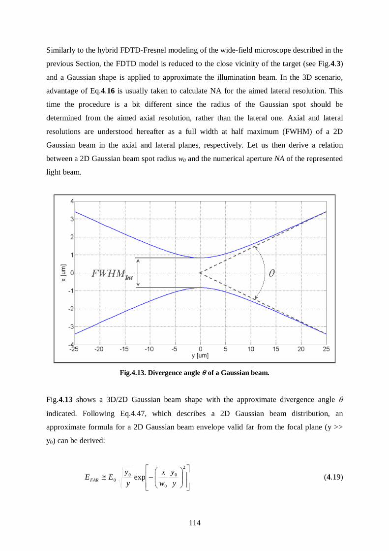
114
Similarly to the hybrid FDTD-Fresnel modeling of the wide-field microscope described in the
previous Section, the FDTD model is reduced to the close vicinity of the target (see Fig.4.3)
and a Gaussian shape is applied to approximate the illumination beam. In the 3D scenario,
advantage of Eq.4.16 is usually taken to calculate NA for the aimed lateral resolution. This
time the procedure is a bit different since the radius of the Gaussian spot should be
determined from the aimed axial resolution, rather than the lateral one. Axial and lateral
resolutions are understood hereafter as a full width at half maximum (FWHM) of a 2D
Gaussian beam in the axial and lateral planes, respectively. Let us then derive a relation
between a 2D Gaussian beam spot radius w0 and the numerical aperture NA of the represented
light beam.
Fig.4.13. Divergence angle θ of a Gaussian beam.
Fig.4.13 shows a 3D/2D Gaussian beam shape with the approximate divergence angle θ
indicated. Following Eq.4.47, which describes a 2D Gaussian beam distribution, an
approximate formula for a 2D Gaussian beam envelope valid far from the focal plane (y >>
y0) can be derived:
−≅
2
0
0
00 exp
yy
wx
yy
EEFAR (4.19)

115
Furthermore, let us derive from the above formula the lateral FWHM of a Gaussian beam far
from the focal plane:
( )0
0, 2lnyywyFWHM FARlat ≅ (4.20)
Thus, the numerical aperture NA is given as follows:
( )( )
5.02
0
0
,2
,
2ln11
25.0
5.0sin
−
+=
+=≅
wy
yFWHMy
yFWHMNA
FARlat
FARlatθ (4.21)
However, the aim is to relate NA with the axial resolution Rax (FWHMax) of a 2D Gaussian
beam, which is given as follows:
0152 yFWHMR axax == (4.22)
Introducing Eqs.4.48,49 and 4.22 into Eq.4.21 leads to the following relations for the
numerical aperture and spot radius, respectively (compare Eq.4.15):
5.0
2ln1521
−
+=
πλ
axRNA (4.23)
1520 πλaxRw = (4.24)
To summarize this Section, application of input and output pinholes allows
achieving increased image contrast, especially in the axial plane, improving the
determination of a 3D shape of the target. It should be emphasized, however, that
confocal microscopy is a sequential image processing method, as it acquires the whole
image pixel by pixel.

116
4.5.2 Hybrid FDTD-Fresnel Modeling of the Confocal Microscope
Hybrid FDTD-Fresnel modeling has already been discussed in Section 4.4.4. Hence, the only
modifications to the hybrid algorithm necessary to properly represent the investigated
problem will be indicated below. The FDTD model is exactly the same as shown in Fig.4.3.
Each simulation run provides, as an outcome, the angular scattering pattern, which is further
processed by the Fresnel-based algorithm onto the image plane. The major discrepancy is in
the different postprocessing of the data obtained from the FDTD simulations since the whole
image is acquired from a pixel-by-pixel execution of several simulations for different
centering of the illumination spot. Regarding illumination source, the Gaussian spot has to be
much narrower than in the wide-field microscope model, so as to resemble the existence of
the input pinhole, which is imaged at the target level.
4.5.3 Computational Tests
Let us consider two complementary targets: a trench and a line processed in a bulk of GaAs
wafer (εr = 10.4976). The height and width of the trench (line) are the same and amount to
10µm, whereas the length of the trench (line) extends to infinity. An image will be processed
at λ = 500nm. Assuming that the target is zo = 2mm from the objective lens and the image
plane is zi = 200mm behind the lens, the focal length amounts to f = 1.98mm.
Since the FDTD model is exactly the same as for the wide-field imaging, basic tests of the
imaging path will be abandoned here. It has been assumed that the spatial discretization step
should not be larger than 200nm, so as to satisfy the Nyquist’s condition at λ = 500nm.
Another step is to choose the expected axial resolution of the imaging system, which will
further allow establishing the radius of the illumination spot (see Eq.4.24) and the width of the
output pinhole. Hence, let us set axial resolution to Rax = 2µm. Thus, according to Eq.4.23,
numerical aperture amounts to NA = 0.547 (θ ≈ 330) and, consequently, the Gaussian beam
radius is w0 = 0.203µm. The same NA will be set for the detection mode.
Let us now compute a point spread function of the detection path (see Fig.4.14). The distance
between the first minima of the PSF is about 108µm, and this value will be set as the width of
the output pinhole.
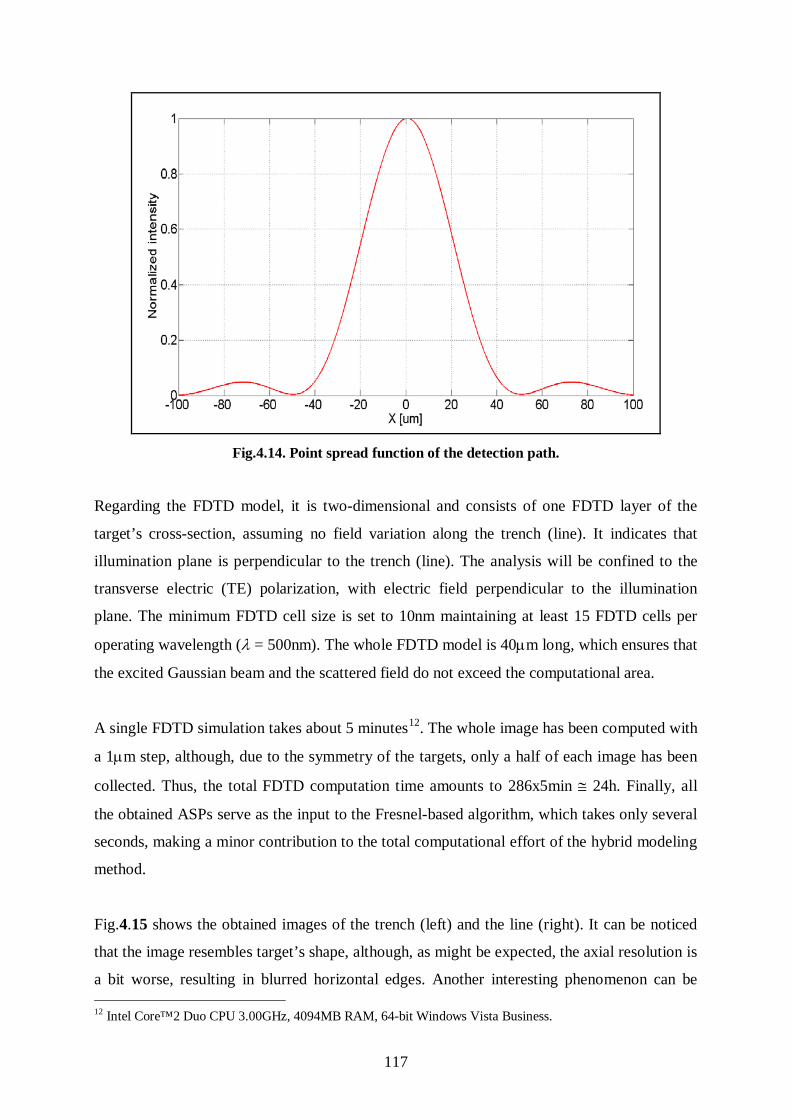
117
Fig.4.14. Point spread function of the detection path.
Regarding the FDTD model, it is two-dimensional and consists of one FDTD layer of the
target’s cross-section, assuming no field variation along the trench (line). It indicates that
illumination plane is perpendicular to the trench (line). The analysis will be confined to the
transverse electric (TE) polarization, with electric field perpendicular to the illumination
plane. The minimum FDTD cell size is set to 10nm maintaining at least 15 FDTD cells per
operating wavelength (λ = 500nm). The whole FDTD model is 40µm long, which ensures that
the excited Gaussian beam and the scattered field do not exceed the computational area.
A single FDTD simulation takes about 5 minutes12
. The whole image has been computed with
a 1µm step, although, due to the symmetry of the targets, only a half of each image has been
collected. Thus, the total FDTD computation time amounts to 286x5min ≅ 24h. Finally, all
the obtained ASPs serve as the input to the Fresnel-based algorithm, which takes only several
seconds, making a minor contribution to the total computational effort of the hybrid modeling
method.
Fig.4.15 shows the obtained images of the trench (left) and the line (right). It can be noticed
that the image resembles target’s shape, although, as might be expected, the axial resolution is
a bit worse, resulting in blurred horizontal edges. Another interesting phenomenon can be 12 Intel Core™2 Duo CPU 3.00GHz, 4094MB RAM, 64-bit Windows Vista Business.
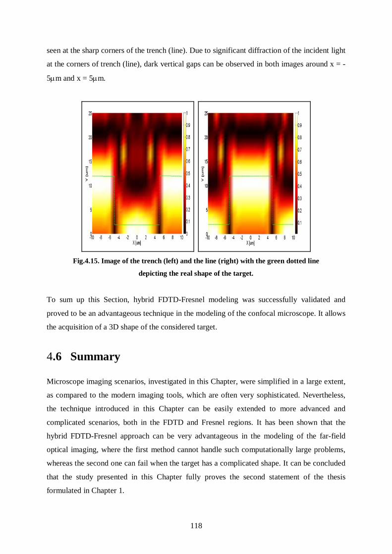
118
seen at the sharp corners of the trench (line). Due to significant diffraction of the incident light
at the corners of trench (line), dark vertical gaps can be observed in both images around x = -
5µm and x = 5µm.
Fig.4.15. Image of the trench (left) and the line (right) with the green dotted line
depicting the real shape of the target.
To sum up this Section, hybrid FDTD-Fresnel modeling was successfully validated and
proved to be an advantageous technique in the modeling of the confocal microscope. It allows
the acquisition of a 3D shape of the considered target.
4.6 Summary
Microscope imaging scenarios, investigated in this Chapter, were simplified in a large extent,
as compared to the modern imaging tools, which are often very sophisticated. Nevertheless,
the technique introduced in this Chapter can be easily extended to more advanced and
complicated scenarios, both in the FDTD and Fresnel regions. It has been shown that the
hybrid FDTD-Fresnel approach can be very advantageous in the modeling of the far-field
optical imaging, where the first method cannot handle such computationally large problems,
whereas the second one can fail when the target has a complicated shape. It can be concluded
that the study presented in this Chapter fully proves the second statement of the thesis
formulated in Chapter 1.

119
Chapter 5
Near-to-Near Transformation in Axisymmetrical Structures
5.1 Introduction
It is well known that a complicated radiating structure can be fully characterized
by a set of electric and magnetic surface currents placed at a closed surface surrounding
the structure (often called the Huygens surface). Knowledge of these currents
(directly related to electric and magnetic fields tangential to the surface) is sufficient
to calculate electromagnetic fields in any test point placed outside the Huygens surface.
Most often that kind of approach is used to perform the so-called near-to-far (NTF)
transformation, consisting in calculation of the fields in the far zone. In NTF transformation,
it can be assumed that:
- all straight lines traced between the test point and any point of the Huygens surface
are parallel,
- fields in the test point do not have radial field components, where “radial” relates
to the spherical coordinate system13
- the distance between the surface current at the Huygens surface and the test point
influences the phase but not the amplitude of the relative contribution of that
current to the field in the test point.
with the origin situated inside the Huygens
surface,
The above assumptions simplify the calculation of the fields in the test point. However,
if test point is relatively close to the Huygens surface, these assumptions cannot be accepted.
In such a case, a much more complicated procedure of calculating fields in the test point has
to be applied. In other words, the so-called near-to-near (NTN) transformation has to be
applied. 13 See Appendix 3.

120
In the case of axisymmetrical problems, denoted also as body of revolution (BOR) problems,
the formulae for numerically effective application of NTF transformation are well known
[80],[81],[82] and applied in commercial software for a long time. In the case of NTN
transformation, the classic approach consists in applying a direct integration of contributions
of the surface currents (placed on cylindrical Huygens surface) in a 3-D space. Such an
approach takes no advantage of the analytically known angular dependence of the currents on
that surface, so computation becomes numerically very ineffective.
This Section describes the new approach to the problem, leading to a very effective numerical
algorithm. That approach is an original contribution of the author of this thesis. Its highlights
were first presented in [83].
5.2 Basic Concept
Axisymmetrical antenna problems are of high importance in the engineering practice. For
instance, corrugated circular waveguide horns or biconical antennas may be recalled. These
horns are often employed as feeds of larger, but also axisymmetrical reflectors. In general,
angular dependence of EM field in axisymmetrical structure may be decomposed into the
following series, given in cylindrical coordinates14
:
( ) ( ) ( ) ( ) ( )∑ +=n
nn nzEnzEzE φρφρφρ cos,sin,,, '
(5.1)
In most practical cases, BOR structures are excited by field patterns of a specific value of n.
Typical example is the circular waveguide mode H11 with n=1. With such an excitation, all
the field components inside a BOR structure are proportional to cos(nφ + φ0), with φ0
dependent on coordinates ρ and z. A 3D problem can be reduced to a 2D one with all EM
components present. Such problems are usually referred to as vector 2D (V2D) in the
cylindrical coordinate system [6], [84], [85].
The major advantage of V2D over 3D approach to BOR problems is that it is much faster and
requires much less computer memory to solve the problem. The difference in both speed and
memory requirements may reach even two orders of magnitude, which is why V2D enables to 14 See Appendix 4.
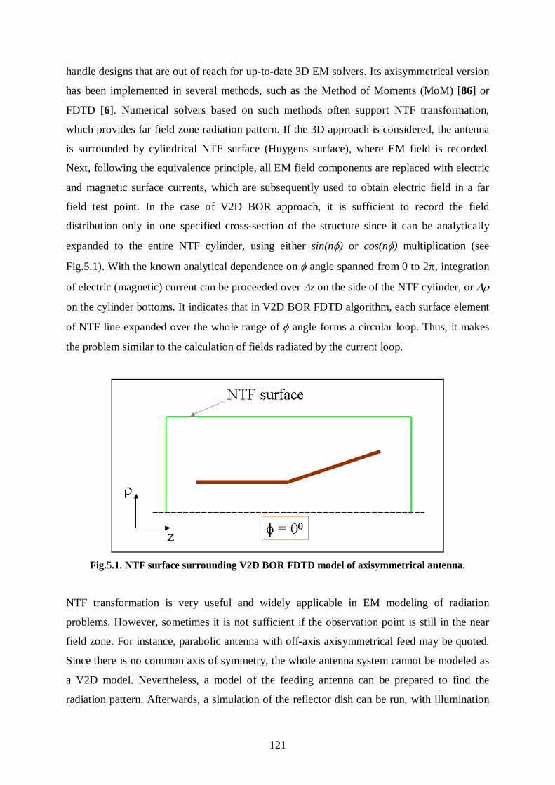
121
handle designs that are out of reach for up-to-date 3D EM solvers. Its axisymmetrical version
has been implemented in several methods, such as the Method of Moments (MoM) [86] or
FDTD [6]. Numerical solvers based on such methods often support NTF transformation,
which provides far field zone radiation pattern. If the 3D approach is considered, the antenna
is surrounded by cylindrical NTF surface (Huygens surface), where EM field is recorded.
Next, following the equivalence principle, all EM field components are replaced with electric
and magnetic surface currents, which are subsequently used to obtain electric field in a far
field test point. In the case of V2D BOR approach, it is sufficient to record the field
distribution only in one specified cross-section of the structure since it can be analytically
expanded to the entire NTF cylinder, using either sin(nφ) or cos(nφ) multiplication (see
Fig.5.1). With the known analytical dependence on φ angle spanned from 0 to 2π, integration
of electric (magnetic) current can be proceeded over ∆z on the side of the NTF cylinder, or ∆ρ
on the cylinder bottoms. It indicates that in V2D BOR FDTD algorithm, each surface element
of NTF line expanded over the whole range of φ angle forms a circular loop. Thus, it makes
the problem similar to the calculation of fields radiated by the current loop.
Fig.5.1. NTF surface surrounding V2D BOR FDTD model of axisymmetrical antenna.
NTF transformation is very useful and widely applicable in EM modeling of radiation
problems. However, sometimes it is not sufficient if the observation point is still in the near
field zone. For instance, parabolic antenna with off-axis axisymmetrical feed may be quoted.
Since there is no common axis of symmetry, the whole antenna system cannot be modeled as
a V2D model. Nevertheless, a model of the feeding antenna can be prepared to find the
radiation pattern. Afterwards, a simulation of the reflector dish can be run, with illumination

122
signal derived from the previously obtained radiation pattern. However, sometimes it cannot
be assumed that the reflector is in the far field zone of the feeding antenna. In such a case,
NTN transformation may be applied in the feed model to obtain distribution of the field that
illuminates reflector.
In principle, BOR NTN transformation can proceed in a similar manner to BOR NTF one
with the Huygens surface reduced to just 3 segments (see Fig.5.1). However, NTN
transformation is more complicated than NTF method since the latter one needs only two
electric field components Eφ and Eθ to be calculated at the test point, as the radial component
does not appear. Moreover, magnetic field is straightforward related to electric one by the free
space impedance. As it has been pointed out earlier in this Chapter, in NTF transformation
some additional approximations can be made, assuming that each point on the NTF surface is
seen under the same angle at the observation point. On the contrary, NTN transformation
imposes calculation of all 6 EM components, without any approximations allowed for NTF
transformation.
Before moving on to the method proposed by the author of this thesis, let us discuss a
straightforward approach to BOR NTN transformation. The concept consists in using BOR
calculation results to collect surface currents on the pickup NTN surface that surrounds
radiating antenna. Then, to obtain the appropriate field component at the test point, a direct
integration of the contribution of these surface currents needs to be performed. However,
although such an approach is robust, it requires a lot of computational effort. Hence, it is
natural to look for a more effective BOR NTN transformation that takes the advantage of
analytically known axial dependence of EM fields (see Eq.5.1). To the knowledge of the
author of this thesis, his paper [83] was the first publicly available consideration of this issue.
Douglas Werner [87] introduced an exact integration procedure for vector potentials
generated by current flowing in a thin circular loop antenna. He considered the current
naturally oriented along φ angle, described by:
( ) ( )'cos' φφ φ nII n= (5.2)
where prime superscript denotes the source coordinates.

123
Werner’s approach is valid in both near and far field zones, and for arbitrary radius a of the
current loop antenna. Later, he extended these results to moderately thick cylindrical wire
antennas [88]. Both solutions refer to the radiation of EM fields into unbounded free space. It
should also be mentioned that Li et al. [89] presented an alternative approach, based on dyadic
Green’s function with separate solutions for regions, where 0 ≤ r ≤ a and r > a.
Let us note that in the BOR NTN transformation, in each of the observation points
contributions of three electric Iρ , Iφ , Iz and three magnetic Kρ , Kφ , Kz current components,
located at the pick-up surface surrounding radiating object, need to be calculated. Werner’s
formulas enable calculation of the contribution of Iφ (φ') component for the specified (ρ, z)
coordinates, and by virtue of duality this can also be extended to Kφ (φ'). To obtain a complete
NTN solution, the method needs to be extended to the remaining components.
5.3 Theoretical Background
As it has already been mentioned, the theoretical background of the analysis below is based
on the approach proposed by Werner [87]. Let us briefly address the relevant issues here. A
view of the considered circular loop antenna is shown in Fig.5.2.
Fig.5.2. Current loop antenna.
124
First of all, a vector potential A is employed to describe EM field components:
AH
×∇=µ1
(5.3)
Hj
E
×∇=ωε1
(5.4)
Let us recall that the vector potential A is related to the source current by the following
formula [73]:
( )∫∫∫=
V
dvRRJA '''
4
πµ
(5.5)
Assuming spherical coordinates notation, magnetic and electric field components are related
to the vector potential A via the following formulae:
( ) ( )
∂∂
−∂∂
= θφ φθ
θθµφθ AA
rrH r sin
sin1,, (5.6)
( ) ( )
∂∂
−∂∂
= φθ φθµφθ Ar
rA
rrH rsin
11,, (5.7)
( ) ( )
∂∂
−∂∂
= rAArrr
rHθµ
φθ θφ1,, (5.8)
( ) ( )
∂∂
−∂∂
= θφ φθ
θθβηφθ HHrj
rEr sinsin
,, (5.9)
( ) ( )
∂∂
−∂∂
= φθ φθβηφθ Hr
rH
rjrE rsin
1,, (5.10)
( ) ( )
∂∂
−∂∂
= rHHrrrj
rEθβ
ηφθ θφ ,, (5.11)
where η denotes intrinsic impedance of the surrounding medium (the air is assumed in this
consideration).

125
Werner proposed to express this vector potential using the following integral:
( ) ( )∫ −=ℑπ
β φφπ
φθ2
0
' ''21,, deIr Rj (5.12)
( ) ( )φφθ ′−−=′ cossin22 arRR (5.13)
where: β is the free space phase constant, R’ is the distance from the source point P`(a,90ο,φ')
to the test point P(r,θ,φ) as shown in Fig.5.2 and:
22 arR += (5.14)
Subsequently, using Lommel's expansions and Euler's identity, Werner derived an exact series
expansion of the integral (Eq.5.12) as follows:
( ) ( ) ( )( ) ( ) ( )( ) 1
21
2
1 00 !
sincos,, −−
∞
=
∞
=
− ∑∑+=ℑ mm
m
m nnmn
Rj
RRh
marnIAeIr
ββθβφφθ β (5.15)
where
122,
021
0
+=−=−
>≥<
=
knmknm
andand
nmnmnm
km
A mmn (5.16)
and ( ) ( )Rhm β2 is the 2nd kind Hankel function of the mth order.
Afterwards, Werner applied this expansion to evaluate exact formulae for the vector potential
components Ar, Aθ, Aφ, given in the spherical coordinates15
15 See Appendix 3.
. Eventually, electric and magnetic
components can be evaluated at the test point using Eqs.5.3,4. Werner restricted his
investigation to one polarization of the current. In the next Section, the contributions of other
current components, i.e.:

126
( ) ( )φφ ρρ ′=′ nII n cos (5.17)
( ) ( )φφ ′=′ nII znz cos (5.18)
will be thoroughly investigated.
5.4 Radial Current Component
Let us express radial current component (Eq.5.17) in the spherical coordinates by employing
unit vectors at the test point P(r,θ,φ):
( ) ( ) ( ) ( ) ( ) ( )φφφφθφφθφ ρφρθρρ ′−−′−+′−=′ sinˆcoscosˆcossinˆ IaIaIaI r (5.19)
If we substitute Eq.5.19 to Eq.5.5, three components of the vector potential are obtained:
( ) ( ) ( )∫ ′′
′−=′−π β
ρ φφφπ
θµφθ2
0
cos4sin,, d
ReIarA
Rj
r (5.20)
( ) ( ) ( )∫ ′′
′−=′−π β
ρθ φφφπ
θµφθ2
0
cos4cos,, d
ReIarA
Rj
(5.21)
( ) ( )∫ ′′
′−−=′−π β
ρφ φφφπ
µφθ2
0
sin4
,, dR
eIarARj
(5.22)
Direct integration of these expressions seems to be extremely time-consuming. Thus, the
problem is approached in a similar way as Werner did in the case of angular current
component. It is presumed that the radial current component can also be expressed as a
function of the integral given by Eq.5.12. Thorough comparison of Eq.5.12 and Eqs.5.20-22
leads to the following relations:
( ) ( ) ( )φθθβ
θµφθ ,,2tan,, r
dd
rjrAr ℑ= (5.23)
127
( ) ( )φθθβ
µφθθ ,,2
,, rdd
rjrA ℑ= (5.24)
( ) ( ) ( )φθφθβ
µφθφ ,,sin2
,, rdd
rjrA ℑ= (5.25)
Finally, introducing series expansion of the integral (see Eq.5.15) into above formulae and
employing Eqs.5.3,4 expressed in spherical coordinates, the following set of expressions has
been derived:
( ) 0,, ≡φθrHr (5.26)
( ) ( ) ( ) ( )( )∑
∞
=
−
−=
1
1
!1/sincos
2cos,,
m
m
mnn mRarAnI
RjrarH θβφθββφθφ
( ) ( ) ( ) ( )
−+× −− Rh
RmRh mm β
ββ 2
12
221 (5.27)
( ) ( )( ) ( ) ( )∑∞
=
−
=1
1
!/sincos
2,,
m
m
mnn mRarAnnI
jRrarH θβφββφθθ
( ) ( ) ( ) ( )
−+× −− Rh
RmRh mm β
ββ 2
12
221 (5.28)
( ) ( ) ( )∑∞
=
−
−=1
2
2
20
!/sincos
2,,
m
m
mnnr mRarAnI
RraZrE θβφβφθ
( ) ( )[ ] ( ) ( ) ( ) ( )
−
++−−× −− RhR
mRhmmnm mm βββθ 21
22
222 21sin1 (5.29)
( ) ( ) ( )∑∞
=
−
−=1
1
20
!/sinsin
2,,
m
m
mnn mRarAnnI
RZarE θβφφθφ
( ) ( ) ( ) ( ) ( ) ( ) ( ) ( )
+
−+−+× −− Rhm
RrmmRhr mm βββ 2
1
22
32 21121 (5.30)

128
( ) ( ) ( ) ( )( )∑
∞
=
−
−=
1
1
20
!1/sincos
2cos,,
m
m
mnn mRarAnI
RZarE θβφθφθθ
( ) ( ) ( ) ( ) ( ) ( ) ( )
+
−
++++× −− Rhm
RrmRRhr mm ββββ 2
2
22
32 2121
( ) ( ) ( ) ( ) ( )
+
−+−+ − Rhm
Rrmm m β2
1
2
21121 (5.31)
Derivation of these expressions was very laborious and they look quite complicated.
However, as it will be shown, due to the presence of factorial term m! in denominators,
computation of the series quickly converges. For relatively small loops (up to about 4
wavelengths), usage of 20 series terms is usually sufficient. For larger loops, the required
number of terms may be higher, but does not exceed 100 the for most practical situations.
5.5 Transverse Current Component
Now, let us present the solution for z-polarized electric current:
( ) ( ) ( )θθφ θ sinˆcosˆ zzrz IaIaI −=′ (5.32)
As previously, the vector potential is expressed as a function of the integral (see Eq.5.15):
( ) ( ) ( ) ( ) ( )
ℑ−ℑ= φθθφθ
θθ
βµφθ ,,cos,,sin
2,, r
drdr
dd
rrjarAr (5.33)
( ) ( ) ( ) ( ) ( ) ( )
ℑ−ℑ−= φθθφθ
θθθ
βµφθθ ,,sin,,tansin
2,, r
drdr
dd
rrjarA (5.34)
( ) 0,, ≡φθφ rA (5.35)
Eventually, it leads to the following expressions for magnetic and electric components at the
test point:

129
( ) ( ) ( ) ( ) ( )∑∞
=
−
=1
12
!/sinsin
2sin,,
m
m
mnnr mRarAnIn
RjarH θβφθβφθ
( ) ( ) ( ) ( )
−+× −− Rh
RmRh mm β
ββ 2
12
221
(5.36)
( ) ( ) ( ) ( ) ( )∑∞
=
−
=1
12
!/sinsin
2cos,,
m
m
mnn mRarAnIn
RjarH θβφθβφθθ
( ) ( ) ( ) ( )
−+× −− Rh
RmRh mm β
ββ 2
12
221
(5.37)
( ) ( ) ( )∑∞
=
−
=1
1
2
2
!/sincos
2,,
m
m
mnn mRarAnI
RjarH θβφβφθφ
( )( ) ( ) ( ){ ( ) ( ) ( ) ( )RhmR
rmRRhr mm βθββθβ 22
22
32 21sin2sin −−
−
++×
( ) ( ) ( ) ( ) ( )
+
−−+ − Rhm
Rrmm m βθ 2
1
2
21sin21 (5.38)
( ) ( ) ( ) ( ) ( )2!
/sincos4
2sin,,1
1
4
20 +−= ∑
∞
=
−
mm
RarAnIR
raZrEm
m
mnnrθβφθφθ
( ) ( ) ( ) ( ) ( ) ( ) ( )( ) ( ) ( )}{ RhmmRhmRRhR mmm βββββ 21
22
23
2 2121212 −−− +−−−+×
( ) ( ) ( )∑
∞
=
−
−2
2
3
30
!/sincos
2cos
m
m
mnn mRarAnI
RaZ θβφθβ
( ) ( ) ( ) ( ) ( ) ( )[ ]RhmRhRnm mm βββ 21
22
22 21 −− −+− (5.39)

130
( ) ( )φφθθ nIRZrarE n cos
2,, 4
02
−=
( ) ( )( ) ( ) ( ){ RhrR
mRarA m
m
m
mn βθββθβ 24
2
1
1
sin!
/sin−
∞
=
−
−∑
( ) ( ) ( ) ( ) ( ) ( )RhmmRrmR m βθβ 2
3
222 2213sin −
+
++
−−
( ) ( ) ( ) ( ) ( ) ( )RhmRrmmmR m βθβ 2
2
22 221322sin21 −
+
+−+−−
( )( ) ( ) ( ) ( ) ( ) ( )
+
+−++−+ − Rhm
Rrmmmm m βθ 2
1
22 322sin2121
( ) ( ) ( )∑
∞
=
−
−2
2
30
3
!/sincos
2sin
m
m
mnn mRraAnI
RZa θβφθβ
( ) ( ) ( ) ( ) ( ) ( )[ ]RhmRhRmn mm βββ 21
22
22 21 −− −+−× (5.40)
( ) ( ) ( ) ( )∑∞
=
−
−=1
1
40
2
!/sinsin
2cos,,
m
m
mnn mRarAnIn
RZrarE θβφθφθφ
( ) ( ) ( ) ( )( ) ( ) ( ){ RhRmRhR mm ββββ 22
23
2 212 −− −+
( )( ) ( ) ( )}Rhmm m β212121 −+−− (5.41)
The above expressions are relatively complex but, as will be shown in the forthcoming
example, they require much less computational effort than the direct integration procedure.
Besides, let us note that although several Hankel functions appear in all the above
expressions, they have the same argument, so the Hankel functions of different order may be
effectively calculated using recursive algorithm.

131
5.6 Benchmark Tests
Three types of independent tests will be run to investigate the accuracy and convergence rate
of Eqs.5.26-31,36-41. These tests can be grouped into the following categories:
1. convergence as a function of series terms (m = 1,2,…,M);
2. available speedup when compared to the direct integration procedure;
3. asymptotic convergence to the NTF transformation.
Formulae for the contribution of Iρ (φ') and Iz (φ') to 6 EM components at the test point have
been derived. All twelve formulae were thoroughly tested against direct numerical integration
and in all cases convergence has been obtained. For the purpose of this Section, the focus is
on the Iz(φ’) contribution to the Hφ component (see Eq.5.38), as a representative case.
Fig.5.3. Magnitude of magnetic field |Hφ| as a function of relative distance r from the loop center
(see Eq.5.38).
Fig.5.3 presents Iz(φ’) contribution to Hφ component, computed using Eq.5.38, assuming the
loop radius equals to the wavelength (a = λ). The results are drawn as a function of distance r
from the loop center, assuming that the test point is seen at the angles θ=π/4 and φ=π/4. Next,
computation with different number of summation terms M has been run, and the obtained
results have been compared with the ones obtained using direct integration in 3D space, with
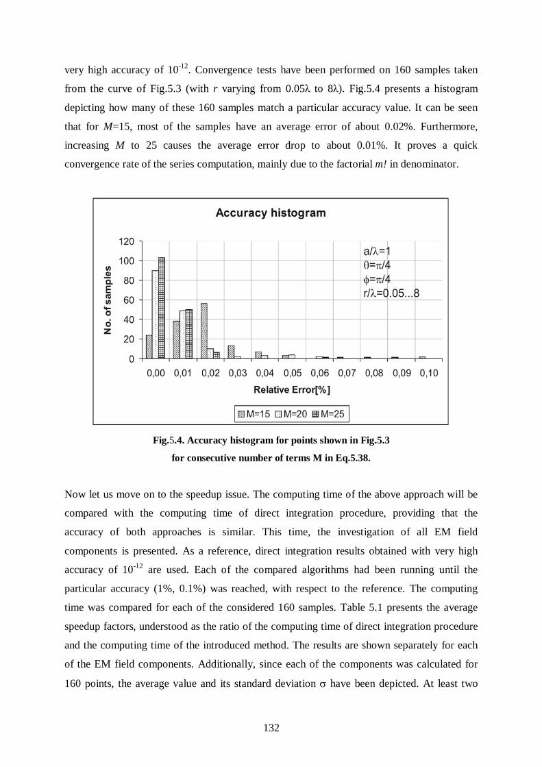
132
very high accuracy of 10-12. Convergence tests have been performed on 160 samples taken
from the curve of Fig.5.3 (with r varying from 0.05λ to 8λ). Fig.5.4 presents a histogram
depicting how many of these 160 samples match a particular accuracy value. It can be seen
that for M=15, most of the samples have an average error of about 0.02%. Furthermore,
increasing M to 25 causes the average error drop to about 0.01%. It proves a quick
convergence rate of the series computation, mainly due to the factorial m! in denominator.
Fig.5.4. Accuracy histogram for points shown in Fig.5.3
for consecutive number of terms M in Eq.5.38.
Now let us move on to the speedup issue. The computing time of the above approach will be
compared with the computing time of direct integration procedure, providing that the
accuracy of both approaches is similar. This time, the investigation of all EM field
components is presented. As a reference, direct integration results obtained with very high
accuracy of 10-12 are used. Each of the compared algorithms had been running until the
particular accuracy (1%, 0.1%) was reached, with respect to the reference. The computing
time was compared for each of the considered 160 samples. Table 5.1 presents the average
speedup factors, understood as the ratio of the computing time of direct integration procedure
and the computing time of the introduced method. The results are shown separately for each
of the EM field components. Additionally, since each of the components was calculated for
160 points, the average value and its standard deviation σ have been depicted. At least two
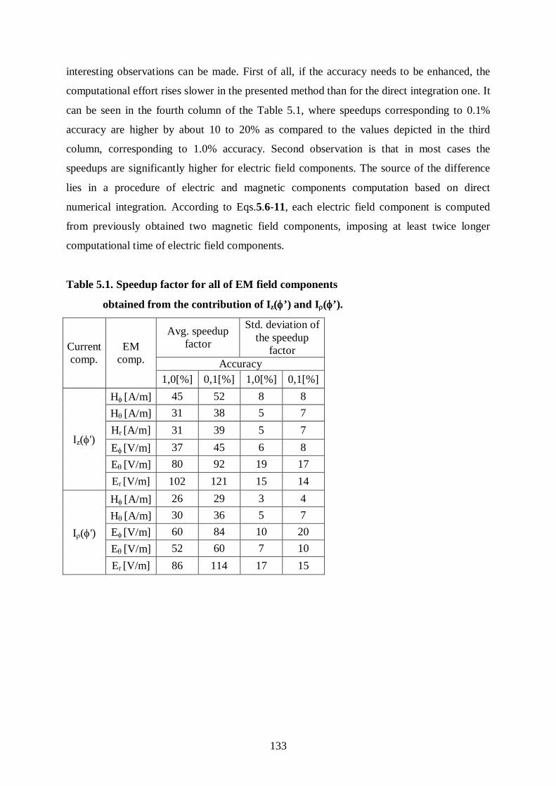
133
interesting observations can be made. First of all, if the accuracy needs to be enhanced, the
computational effort rises slower in the presented method than for the direct integration one. It
can be seen in the fourth column of the Table 5.1, where speedups corresponding to 0.1%
accuracy are higher by about 10 to 20% as compared to the values depicted in the third
column, corresponding to 1.0% accuracy. Second observation is that in most cases the
speedups are significantly higher for electric field components. The source of the difference
lies in a procedure of electric and magnetic components computation based on direct
numerical integration. According to Eqs.5.6-11, each electric field component is computed
from previously obtained two magnetic field components, imposing at least twice longer
computational time of electric field components.
Table 5.1. Speedup factor for all of EM field components
obtained from the contribution of Iz(φ’) and Iρ(φ’).
Current comp.
EM comp.
Avg. speedup factor
Std. deviation of the speedup
factor Accuracy
1,0[%] 0,1[%] 1,0[%] 0,1[%]
Iz(φ')
Hφ [A/m] 45 52 8 8 Hθ [A/m] 31 38 5 7 Hr [A/m] 31 39 5 7 Eφ [V/m] 37 45 6 8 Eθ [V/m] 80 92 19 17 Er [V/m] 102 121 15 14
Iρ(φ')
Hφ [A/m] 26 29 3 4 Hθ [A/m] 30 36 5 7 Eφ [V/m] 60 84 10 20 Eθ [V/m] 52 60 7 10 Er [V/m] 86 114 17 15

134
Fig.5.5. Comparison between Eq.5.38 and corresponding NTF solution.
The last investigation focuses on the asymptotic convergence of the NTN solution to the NTF
one [80]. Fig.5.5 shows both curves in a logarithmic scale. It is clearly observable that the
NTN transformation tends to the NTF one, and for the distance larger than about 6-7
wavelengths discrepancy is barely visible, which indicates that it is the far field zone limit.
5.7 Summary
Analytically preprocessed formulae for the effective near-to-near transformation of
axisymmetrical problems have been presented. The obtained results show that a speedup by a
factor of about 30 to 100 can be obtained, with respect to direct integration in 3-D space in
practical cases of Huygens surfaces of the size of a few wavelengths. These results appear to
be very attractive when practical applications are concerned. Thus, the third auxiliary thesis
posed in Chapter 1 has been successfully proven.
135
Chapter 6
Conclusions and perspectives
This dissertation has been focused on extension of the finite-difference time-domain method
and its computational capabilities, by supplementing the method with analytical formulations
appropriate for specific electromagnetic problems. Three types of the problems have been
considered in this thesis:
1. 1D, 2D, and 3D periodic structures;
2. far-field optical microscope imaging;
3. near-to-near electromagnetic field transformation in axisymmetrical structures.
The first issue is an extension of methods and algorithms already known from the literature.
Considerations of the author of this thesis have been focused on CL-FDTD algorithm.
Implementation of the algorithm has been extended from 1D to 2D and 3D periodicity, and
successful validation has been performed. The method has been further applied to the analysis
of eigenvalues problems in the infinitely periodic structures. It has been proved to be a useful
technique for investigation of dispersive properties of photonic crystals. Afterwards, an
extension of the CL-FDTD algorithm to the analysis of plane wave diffraction from infinitely
periodic structure has been shown. For that purpose, three computational models have been
proposed and thoroughly validated against other numerical methods, such as Finite Element
Method, Plane Wave Expansion, Rigorous Coupled Wave Analysis, and analytical
formulations. It has also been shown that approximate approach with an infinite plane wave
over periodic structure is convergent to the real case with a finite spot of a Gaussian shape.
With growing interest in photonic crystals from optics, through millimeter wave technology,
to microwaves, the scope of potential applications of the computational methods like
CL-FDTD will be extending. However, it seems that more challenging will be another issue
addressed in the context of periodic structures, i.e. scatterometry. First of all, single frequency
operation in CL-FDTD models for a plane wave illumination of periodic structures is their
major limitation. Additionally, it would be an interesting option to develop a source with an

136
arbitrary shape of a beam impinging on infinite periodic structure. As it has been pointed out
in Chapter 3, some preliminary studies have already been published.
The second type of problems addressed in this dissertation deals with electromagnetic
modeling of the far-field optical microscopes that utilize lenses as image-processing devices.
A theoretical knowledge about an image formation in lens microscopes is very well
established and thoroughly examined. However, imaging tools are still under development,
driven by the science and industry’s demand for still increasing resolution. It forces the
modeling methods to improve their computational capabilities, as well as the achievable
accuracy. This is a proper place for full-wave electromagnetic design, especially at the target
level where subwavelength diffraction plays an important role. It has been proposed in this
dissertation to couple the full-wave finite-difference time-domain technique with the optical
method based on Fresnel approximation of the diffraction phenomenon. Such approach
combines advantages of both methods, increasing the achieavable accuracy without a
tremendous impact on the computation time. It has been proven to be useful in the modeling
of wide field, as well as confocal optical microscopes.
There is a lot of perspectives for the finite-difference time-domain method, as well as for the
other full-wave approaches to find new fields of application in the optical imaging. With
growing capabilities of computing machines, it will be possible to extend the complexity of
FDTD models and their computational volume. Another important issue that has already
found some attention of researchers is the modeling of sources which properly represent time-
dependent electromagnetic field distribution focused by a lens without loss of causality.
Successful research in this field will help to improve appropriate represenation of
electromagnetic field in the finite-difference time-domain schemes.
The last but definitely not least subject addressed in this thesis is strictly related to the
modeling of axisymmetrical antennae. An efficient method for electromagnetic field
transformations in a near zone of a radiating axisymmetrical object has been derived and
validated with theoretical calculations. The method can be useful for the modeling of the
axisymmetrical antenna systems with no common symmetry axis, like in the case of
Cassegrain antenna with a feeding antenna shifted off the axis.

137
The method presented in this thesis waits for its implementation in the finite-difference time-
domain scheme or other computational methods applied to axisymmetrical problems.
To summarize the whole dissertation, thesis posed in Chapter 1, claiming that the partially
analytical FDTD method can improve computational efficiency of the overall method has
been proven. The auxiliary statements regarding periodic structures, microscope imaging, and
near-to-near field transformation for axisymmetrical problems have also been thoroughly
investigated and confirmed.

138
Appendix 1
Periodic Boundary Conditions
A schematic flow of the FDTD algorithm for periodic boundary conditions is given below.
Notation is based on C language.
for (FDTD_iteration==1; FDTD_iteration>0; FDTD_iteration++){
//E calculation with FDTD algorithm
...
switch (periodicity){
case x:
Ey_re(N-1,:,:) = Ey_re(1,:,:)*cos(ψx) - Ey_im(1,:,:)*sin(ψx);
Ey_im(N-1,:,:) = Ey_im(1,:,:)*cos(ψx) + Ey_re(1,:,:)*sin(ψx);
Ez_re(N-1,:,:) = Ez_re(1,:,:)*cos(ψx) - Ez_im(1,:,:)*sin(ψx);
Ez_im(N-1,:,:) = Ez_im(1,:,:)*cos(ψx) + Ez_re(1,:,:)*sin(ψx);
break;
case y:
Ex_re(:,M-1,:) = Ex_re(:,1,:)*cos(ψy) - Ex_im(:,1,:)*sin(ψy);
Ex_im(:,M-1,:) = Ex_im(:,1,:)*cos(ψy) + Ex_re(:,1,:)*sin(ψy);
Ez_re(:,M-1,:) = Ez_re(:,1,:)*cos(ψy) - Ez_im(:,1,:)*sin(ψy);
Ez_im(:,M-1,:) = Ez_im(:,1,:)*cos(ψy) + Ez_re(:,1,:)*sin(ψy);
break;
case z:
Ex_re(:,:,P-1) = Ex_re(:,:,1)*cos(ψz) - Ex_im(:,:,1)*sin(ψz);
Ex_im(:,:,P-1) = Ex_im(;,:,1)*cos(ψz) + Ex_re(:,:,1)*sin(ψz);
Ey_re(:,:,P-1) = Ey_re(:,:,1)*cos(ψz) - Ey_im(:,:,1)*sin(ψz);
Ey_im(:,:,P-1) = Ey_im(;,:,1)*cos(ψz) + Ey_re(:,:,1)*sin(ψz);
break;
case xy:
Ey_re(N-1,:,:) = Ey_re(1,:,:)*cos(ψx) - Ey_im(1,:,:)*sin(ψx);

139
Ey_im(N-1,:,:) = Ey_im(1,:,:)*cos(ψx) + Ey_re(1,:,:)*sin(ψx);
Ez_re(N-1,:,:) = Ez_re(1,:,:)*cos(ψx) - Ez_im(1,:,:)*sin(ψx);
Ez_im(N-1,:,:) = Ez_im(1,:,:)*cos(ψx) + Ez_re(1,:,:)*sin(ψx);
Ex_re(:,M-1,:) = Ex_re(:,1,:)*cos(ψy) - Ex_im(:,1,:)*sin(ψy);
Ex_im(:,M-1,:) = Ex_im(:,1,:)*cos(ψy) + Ex_re(:,1,:)*sin(ψy);
Ez_re(:,M-1,:) = Ez_re(:,1,:)*cos(ψy) - Ez_im(:,1,:)*sin(ψy);
Ez_im(:,M-1,:) = Ez_im(:,1,:)*cos(ψy) + Ez_re(:,1,:)*sin(ψy);
break;
case xz:
Ey_re(N-1,:,:) = Ey_re(1,:,:)*cos(ψx) - Ey_im(1,:,:)*sin(ψx);
Ey_im(N-1,:,:) = Ey_im(1,:,:)*cos(ψx) + Ey_re(1,:,:)*sin(ψx);
Ez_re(N-1,:,:) = Ez_re(1,:,:)*cos(ψx) - Ez_im(1,:,:)*sin(ψx);
Ez_im(N-1,:,:) = Ez_im(1,:,:)*cos(ψx) + Ez_re(1,:,:)*sin(ψx);
Ex_re(:,:,P-1) = Ex_re(:,:,1)*cos(ψz) - Ex_im(:,:,1)*sin(ψz);
Ex_im(:,:,P-1) = Ex_im(;,:,1)*cos(ψz) + Ex_re(:,:,1)*sin(ψz);
Ey_re(:,:,P-1) = Ey_re(:,:,1)*cos(ψz) - Ey_im(:,:,1)*sin(ψz);
Ey_im(:,:,P-1) = Ey_im(;,:,1)*cos(ψz) + Ey_re(:,:,1)*sin(ψz);
break;
case yz:
Ex_re(:,M-1,:) = Ex_re(:,1,:)*cos(ψy) - Ex_im(:,1,:)*sin(ψy);
Ex_im(:,M-1,:) = Ex_im(:,1,:)*cos(ψy) + Ex_re(:,1,:)*sin(ψy);
Ez_re(:,M-1,:) = Ez_re(:,1,:)*cos(ψy) - Ez_im(:,1,:)*sin(ψy);
Ez_im(:,M-1,:) = Ez_im(:,1,:)*cos(ψy) + Ez_re(:,1,:)*sin(ψy);
Ex_re(:,:,P-1) = Ex_re(:,:,1)*cos(ψz) - Ex_im(:,:,1)*sin(ψz);
Ex_im(:,:,P-1) = Ex_im(;,:,1)*cos(ψz) + Ex_re(:,:,1)*sin(ψz);
Ey_re(:,:,P-1) = Ey_re(:,:,1)*cos(ψz) - Ey_im(:,:,1)*sin(ψz);
Ey_im(:,:,P-1) = Ey_im(;,:,1)*cos(ψz) + Ey_re(:,:,1)*sin(ψz);
break;
case xyz:
Ey_re(N-1,:,:) = Ey_re(1,:,:)*cos(ψx) - Ey_im(1,:,:)*sin(ψx);
Ey_im(N-1,:,:) = Ey_im(1,:,:)*cos(ψx) + Ey_re(1,:,:)*sin(ψx);
Ez_re(N-1,:,:) = Ez_re(1,:,:)*cos(ψx) - Ez_im(1,:,:)*sin(ψx);
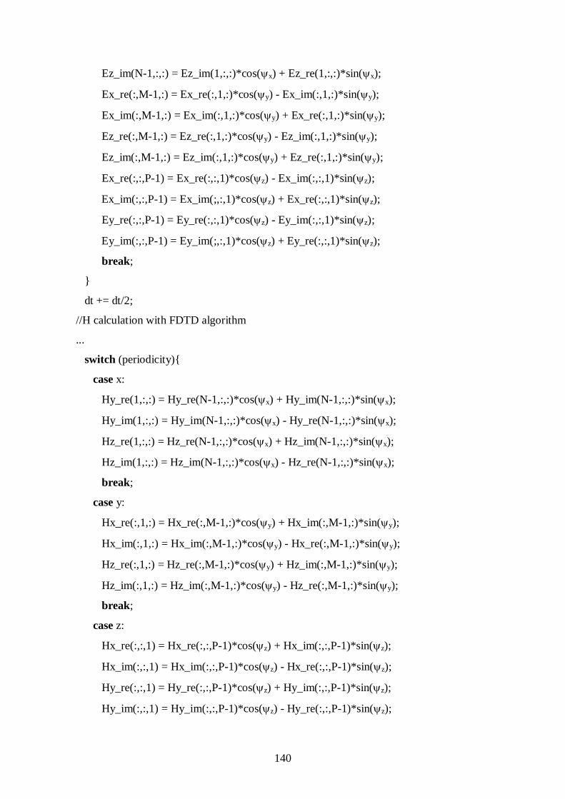
140
Ez_im(N-1,:,:) = Ez_im(1,:,:)*cos(ψx) + Ez_re(1,:,:)*sin(ψx);
Ex_re(:,M-1,:) = Ex_re(:,1,:)*cos(ψy) - Ex_im(:,1,:)*sin(ψy);
Ex_im(:,M-1,:) = Ex_im(:,1,:)*cos(ψy) + Ex_re(:,1,:)*sin(ψy);
Ez_re(:,M-1,:) = Ez_re(:,1,:)*cos(ψy) - Ez_im(:,1,:)*sin(ψy);
Ez_im(:,M-1,:) = Ez_im(:,1,:)*cos(ψy) + Ez_re(:,1,:)*sin(ψy);
Ex_re(:,:,P-1) = Ex_re(:,:,1)*cos(ψz) - Ex_im(:,:,1)*sin(ψz);
Ex_im(:,:,P-1) = Ex_im(;,:,1)*cos(ψz) + Ex_re(:,:,1)*sin(ψz);
Ey_re(:,:,P-1) = Ey_re(:,:,1)*cos(ψz) - Ey_im(:,:,1)*sin(ψz);
Ey_im(:,:,P-1) = Ey_im(;,:,1)*cos(ψz) + Ey_re(:,:,1)*sin(ψz);
break;
}
dt += dt/2;
//H calculation with FDTD algorithm
...
switch (periodicity){
case x:
Hy_re(1,:,:) = Hy_re(N-1,:,:)*cos(ψx) + Hy_im(N-1,:,:)*sin(ψx);
Hy_im(1,:,:) = Hy_im(N-1,:,:)*cos(ψx) - Hy_re(N-1,:,:)*sin(ψx);
Hz_re(1,:,:) = Hz_re(N-1,:,:)*cos(ψx) + Hz_im(N-1,:,:)*sin(ψx);
Hz_im(1,:,:) = Hz_im(N-1,:,:)*cos(ψx) - Hz_re(N-1,:,:)*sin(ψx);
break;
case y:
Hx_re(:,1,:) = Hx_re(:,M-1,:)*cos(ψy) + Hx_im(:,M-1,:)*sin(ψy);
Hx_im(:,1,:) = Hx_im(:,M-1,:)*cos(ψy) - Hx_re(:,M-1,:)*sin(ψy);
Hz_re(:,1,:) = Hz_re(:,M-1,:)*cos(ψy) + Hz_im(:,M-1,:)*sin(ψy);
Hz_im(:,1,:) = Hz_im(:,M-1,:)*cos(ψy) - Hz_re(:,M-1,:)*sin(ψy);
break;
case z:
Hx_re(:,:,1) = Hx_re(:,:,P-1)*cos(ψz) + Hx_im(:,:,P-1)*sin(ψz);
Hx_im(:,:,1) = Hx_im(:,:,P-1)*cos(ψz) - Hx_re(:,:,P-1)*sin(ψz);
Hy_re(:,:,1) = Hy_re(:,:,P-1)*cos(ψz) + Hy_im(:,:,P-1)*sin(ψz);
Hy_im(:,:,1) = Hy_im(:,:,P-1)*cos(ψz) - Hy_re(:,:,P-1)*sin(ψz);

141
break;
case xy:
Hy_re(1,:,:) = Hy_re(N-1,:,:)*cos(ψx) + Hy_im(N-1,:,:)*sin(ψx);
Hy_im(1,:,:) = Hy_im(N-1,:,:)*cos(ψx) - Hy_re(N-1,:,:)*sin(ψx);
Hz_re(1,:,:) = Hz_re(N-1,:,:)*cos(ψx) + Hz_im(N-1,:,:)*sin(ψx);
Hz_im(1,:,:) = Hz_im(N-1,:,:)*cos(ψx) - Hz_re(N-1,:,:)*sin(ψx);
Hx_re(:,1,:) = Hx_re(:,M-1,:)*cos(ψy) + Hx_im(:,M-1,:)*sin(ψy);
Hx_im(:,1,:) = Hx_im(:,M-1,:)*cos(ψy) - Hx_re(:,M-1,:)*sin(ψy);
Hz_re(:,1,:) = Hz_re(:,M-1,:)*cos(ψy) + Hz_im(:,M-1,:)*sin(ψy);
Hz_im(:,1,:) = Hz_im(:,M-1,:)*cos(ψy) - Hz_re(:,M-1,:)*sin(ψy);
break;
case xz:
Hy_re(1,:,:) = Hy_re(N-1,:,:)*cos(ψx) + Hy_im(N-1,:,:)*sin(ψx);
Hy_im(1,:,:) = Hy_im(N-1,:,:)*cos(ψx) - Hy_re(N-1,:,:)*sin(ψx);
Hz_re(1,:,:) = Hz_re(N-1,:,:)*cos(ψx) + Hz_im(N-1,:,:)*sin(ψx);
Hz_im(1,:,:) = Hz_im(N-1,:,:)*cos(ψx) - Hz_re(N-1,:,:)*sin(ψx);
Hx_re(:,:,1) = Hx_re(:,:,P-1)*cos(ψz) + Hx_im(:,:,P-1)*sin(ψz);
Hx_im(:,:,1) = Hx_im(:,:,P-1)*cos(ψz) - Hx_re(:,:,P-1)*sin(ψz);
Hy_re(:,:,1) = Hy_re(:,:,P-1)*cos(ψz) + Hy_im(:,:,P-1)*sin(ψz);
Hy_im(:,:,1) = Hy_im(:,:,P-1)*cos(ψz) - Hy_re(:,:,P-1)*sin(ψz);
break;
case yz:
Hx_re(:,1,:) = Hx_re(:,M-1,:)*cos(ψy) + Hx_im(:,M-1,:)*sin(ψy);
Hx_im(:,1,:) = Hx_im(:,M-1,:)*cos(ψy) - Hx_re(:,M-1,:)*sin(ψy);
Hz_re(:,1,:) = Hz_re(:,M-1,:)*cos(ψy) + Hz_im(:,M-1,:)*sin(ψy);
Hz_im(:,1,:) = Hz_im(:,M-1,:)*cos(ψy) - Hz_re(:,M-1,:)*sin(ψy);
Hx_re(:,:,1) = Hx_re(:,:,P-1)*cos(ψz) + Hx_im(:,:,P-1)*sin(ψz);
Hx_im(:,:,1) = Hx_im(:,:,P-1)*cos(ψz) - Hx_re(:,:,P-1)*sin(ψz);
Hy_re(:,:,1) = Hy_re(:,:,P-1)*cos(ψz) + Hy_im(:,:,P-1)*sin(ψz);
Hy_im(:,:,1) = Hy_im(:,:,P-1)*cos(ψz) - Hy_re(:,:,P-1)*sin(ψz);
break;
case xyz:

142
Hy_re(1,:,:) = Hy_re(N-1,:,:)*cos(ψx) + Hy_im(N-1,:,:)*sin(ψx);
Hy_im(1,:,:) = Hy_im(N-1,:,:)*cos(ψx) - Hy_re(N-1,:,:)*sin(ψx);
Hz_re(1,:,:) = Hz_re(N-1,:,:)*cos(ψx) + Hz_im(N-1,:,:)*sin(ψx);
Hz_im(1,:,:) = Hz_im(N-1,:,:)*cos(ψx) - Hz_re(N-1,:,:)*sin(ψx);
Hx_re(:,1,:) = Hx_re(:,M-1,:)*cos(ψy) + Hx_im(:,M-1,:)*sin(ψy);
Hx_im(:,1,:) = Hx_im(:,M-1,:)*cos(ψy) - Hx_re(:,M-1,:)*sin(ψy);
Hz_re(:,1,:) = Hz_re(:,M-1,:)*cos(ψy) + Hz_im(:,M-1,:)*sin(ψy);
Hz_im(:,1,:) = Hz_im(:,M-1,:)*cos(ψy) - Hz_re(:,M-1,:)*sin(ψy);
Hx_re(:,:,1) = Hx_re(:,:,P-1)*cos(ψz) + Hx_im(:,:,P-1)*sin(ψz);
Hx_im(:,:,1) = Hx_im(:,:,P-1)*cos(ψz) - Hx_re(:,:,P-1)*sin(ψz);
Hy_re(:,:,1) = Hy_re(:,:,P-1)*cos(ψz) + Hy_im(:,:,P-1)*sin(ψz);
Hy_im(:,:,1) = Hy_im(:,:,P-1)*cos(ψz) - Hy_re(:,:,P-1)*sin(ψz);
break;
}
}
Legend:
1) Indices of all components are written using E(m,n,p) notation, where (m,n,p) indicates
the location of the component on the FDTD grid expanded in a Cartesian (x,y,z) space.
2) The maximum number of FDTD grid points is (N,M,P).
3) Suffixes _re and _im denote real and imaginary parts of EM component, respectively,.
4) The symbol ψ denotes the Floquet phase shift per period - a parameter of the CL-
FDTD algorithm.
5) A symbol dt is the FDTD algorithm’s time step.

143
Appendix 2
Brillouin zone
According to the Bloch’s (or Floquet’s) theorem, propagation of the electromagnetic wave in
a periodic medium can be characterized in the following way:
( ) ( ) rkjkk erur 0
=ψ (1.1)
where uk(r) function has the same periodicity L as the periodic medium:
( ) ( )ruLru kk
=+ (1.2)
and k0 is the wavenumber.
It implies that the solution of ψk(r) function is identical for all the integer multiples of the
wavenumber:
Lnkkn
π20 += (1.3)
Thus, mode frequencies are also periodic in the wave vector space, so the analysis
of the k(ω) dispersion can be limited to the region: -π/L < kn < π/L, usually called
the first Brillouin zone that characterizes primitive cell of the considered reciprocal
lattice. Unique characterization of the dispersion characteristic k(ω) can be
done considering only the so-called irreducible Brillouin zone, understood as
the first Brillouin zone reduced by using all the possible symmetries. Brillouin zone
is parameterized using critical points that refer to the characteristic points of the Brillouin
zone.

144
Let us recall the most common lattice geometries addressed in this thesis:
1. square lattice
(a)
(b)
(c)
Fig.A2.1. Square lattice (a) and the corresponding reciprocal lattice (b) with the irreducible
Brillouin zone (c).
Critical points:
Γ: 0== yx kk .
X: akxπ2= ; 0=yk .
M: akk yxπ2== .

145
2. hexagonal lattice
(a)
(b)
Fig.A2.2. Hexagonal lattice (a) and the corresponding reciprocal lattice (b) with the irreducible
Brillouin zone (c).
Critical points:
Γ: 0== yx kk .
M: 0=xk ; a
k y 32π= .
K: akx 32π= ;
ak y 3
2π= .

146
3. Body centered cubic (bcc) lattice
(a)
(b)
Fig.A2.3. Body centered cubic lattice (a) and the corresponding reciprocal face centered (fcc)
lattice (b).
Critical points:
Γ: 0=== zyx kkk .
H: 0=xk ; ak yπ2= ; 0=zk .
N: akxπ= ; ak y
π= ; 0=zk .
P: akxπ= ; ak y
π= ; akzπ= .

147
Appendix 3
Spherical coordinate system
Fig.A3.1. Spherical coordinate system view.
Relation between rectangular and spherical coordinates:
( ) ( )φθ cossinrx = (3.1)
( ) ( )φθ sinsinry = (3.2)
( )θcosrz = (3.3)
Transition from rectangular to spherical components:
( ) ( ) ( ) ( ) ( )θφθφθ cossinsincossin zyxr AAAA ++= (3.4)
( ) ( ) ( ) ( ) ( )θφθφθθ sinsincoscoscos zyx AAAA ++= (3.5)
( ) ( )ϕφφ cossin yx AAA +−= (3.6)

148
Transition from spherical to rectangular components:
( ) ( ) ( ) ( ) ( )φφθφθ φθ sincoscoscossin AAAA rx −+= (3.7)
( ) ( ) ( ) ( ) ( )φφθφθ φθ cossincossinsin AAAA ry ++= (3.8)
( ) ( )θθ θ sincos AAA rz −= (3.9)

149
Appendix 4
Cylindrical coordinate system
Fig.A4.1. Cylindrical coordinate system view.
Relation between rectangular and cylindrical coordinates:
( )φρ cos=x (4.1)
( )φρ sin=y (4.2)
zz = (4.3)
Transition from rectangular to cylindrical components:
( ) ( )φφρ sincos yx AAA += (4.4)
( ) ( )φφφ cossin yx AAA +−= (4.5)
zz AA = (4.6)

150
Transition from cylindrical to rectangular components:
( ) ( )φφ φρ sincos AAAx −= (4.7)
( ) ( )φφ φρ cossin AAAy += (4.8)
zz AA = (4.9)

151
Appendix 5
Lens imaging algorithm
Below, the procedures for lens imaging based on the Fresnel approximation are given. The
code of those scripts was written by the author of this thesis in Matlab environment.
function Eo = lens_imaging(fname,frequency,start_angle,stop_angle,ref_angle,ds,di,f)
% Eo = lens_imaging(fname,frequency,start_angle,stop_angle,ref_angle,ds,di,f)
% calculates an image processed by a single cylindrical lens
% upon angular scatterring pattern provided by the user in (fname) file.
%
% Input data should consist of three columns with an angle (degrees),
% and corresponding electric field intensity magnitude and phase (degrees).
%
% frequency - operating frequency, GHz
% start_angle -
% stop_angle - these two values define numerical aperture of a considered
% beam taken from the file, degrees
% ref_angle - reference angle, degrees
% ds - distance from object plane to the lens, mm
% di - distance from the lens to image plane, mm
% f - focal length of the lens, mm
format long g
deg2rad = pi/180;
rad2deg = 180/pi;
%read data from file
A = load(fname);
%wavenumber

152
k = 2*pi*frequency/299.792458; %[1/mm]
ys=0; %[mm] - radiation from the focal point
dang=0.00001;% angular resolution
start_angle_ind = find((A(:,1)>=(start_angle-dang))&(A(:,1)<=(start_angle+dang)));
stop_angle_ind = find((A(:,1)>=(stop_angle-dang))&(da3_data(:,1)<=(stop_angle+dang)));
%electric field at source plane
Es=A(start_angle_ind:stop_angle_ind,2) .*
exp(j*deg2rad.*A(start_angle_ind:stop_angle_ind,4));
%find maximum angle...
alfa_max=A(stop_angle_ind)-ref_angle;%[deg]
%calculate numerical aperture
NA = sin(deg2rad*alfa_max);
%calculate spatial range at the lens
ys_max = tan(deg2rad*alfa_max)*ds;%[mm]
% space vector discretization for a given resolution...
pow=10;
N=2^pow;
dys_min = pi*ds/(k*ys_max);
dys = (2*ys_max/(N-1));%[mm]
while dys>=dys_min
pow=pow+1;
N=2^pow;
dys = (2*ys_max/(N-1));%[mm]
end
ys=-ys_max:dys:ys_max;
fy = -(N-1)/(2*N*dys):1/(N*dys):(N-1)/(2*N*dys);
% interpolation of electric field at newly discretized spatial vector
alfa_p=rad2deg.*atan(ys./ds);
Es_abs=interp1(da3_data(start_angle_ind:stop_angle_ind,1)-
ref_angle,abs(Es),alfa_p,'linear');

153
Es_angle=interp1(da3_data(start_angle_ind:stop_angle_ind,1)-
ref_angle,angle(Es),alfa_p,'linear');
Us_FT = Es_abs.*exp(j.*Es_angle);
%impulse response of space between source and lens planes
hfr = h_fr_air(k,ds,ys);
HFR = (1/N)*fft(hfr);
HFR = fftshift(HFR);
% lens contribution
tfl = t_lens(k,f,ys);
%impulse response of space between lens and image planes
hfr1 = h_fr_air(k,di,ys);
HFR1 = (1/N)*fft(hfr1);
HFR1 = fftshift(HFR1);
%transformation from source plane to lens plane
Elens = N*ifft(Us_FT.*HFR);
%transformation through the lens
Elens = Elens.*tfl;
Elens_FT = (1/N)*fft(Elens);
%transformation from lens plane to image plane
Eo_FT = Elens_FT.*HFR1;
%transformation from angular space to Cartesian space
Eo = N*ifft(Eo_FT);
Eo = fftshift(Eo);
**************************
function h = h_fr_air(k,d,y)
% Fresnel approximation of the open air impulse response
%
% k – wavenumber, 1/mm
% d – distance, mm
% y – shift distance from the lens axis, mm

154
format long g
h = k.*exp(j*k*d).*exp( 0.5.*j.*k.*y.^2./d )./(2*pi*j*d);
**************************
function U = t_lens(k,f,y)
% thin lens approximation
%
% k – wavenumber, 1/mm
% f – focal length of the lens, mm
% y – shift distance from the lens axis, mm
format long g
U = exp( -0.5.*j.*k.*y.^2./f );
155
Bibliography
[1] K. Yee, “Numerical Solution of Initial Boundary Value Problems Involving Maxwell's
Equations in Isotropic Media”, IEEE Trans. on Antennas and Propagation, Vol.14,
May 1966.
[2] A. Taflove, S. C. Hagness, Computational Electrodynamics: The Finite-Difference
Time-Domain Method, (Artech House Publishers, 2005).
[3] G. Mur, “Absorbing Boundary Conditions for the Finite-Difference Approximation of
the Time-Domain Electromagnetic-Field Equations,” IEEE Trans. Electromagnetic
Compatibility, vol. EMC-23, no.4, pp. 377-382, Nov. 1981.
[4] J. P. Berenger, “A perfectly matched layer for the absorption of electromagnetic
waves,” J. Comput. Phys., vol. 114, no. 2, pp. 185-200, Oct. 1994.
[5] K. K. Mei., J. Fana. "Superabsorption - A Method to Improve Absorbing Boundary
Conditions," IEEE Trans. Antennas & Propagat., vol. AP-40, pp. 1001-1010, Sept.
1992.
[6] W. K. Gwarek, T. Morawski, C. Mroczkowski, “Application of the FDTD Method to
the Analysis of the Circuits Described by the Two-Dimensional Vector Wave
Equation,” IEEE Trans. Microwave Theory Tech., vol. 41, no. 2, pp. 311-316, Feb.
1993.
[7] W. K. Gwarek, M. Celuch-Marcysiak, “A differential method of reflection coefficient
extraction from FD-TD simulations,” IEEE MicrowaveGuided Wave Lett., vol. 6, pp.
215–217, May 1996.
[8] A. Kreczkowski, M. Mrozowski, “Multimode analysis of waveguide discontinuities
using the concept of generalized scattering matrix and power waves,” Proc. 13th Int.
MIKON Conf., Wroclaw, Poland, May 2000, pp. 569–572.
[9] D. E. Merewether, R. Fisher, F. W. Smith, “On Implementing a Numeric Huygen’s
Source Scheme in a Finite Difference Program to Illuminate Scattering Bodies”, IEEE
Trans. Nuclear Science, vol. 27, no. 6, Dec. 1980, pp.1829-1833.
[10] L-C. Ma, R. Mittra, “Implementation of Gaussian Beam Sources in FDTD for
Scattering Problems”, IEEE Trans. Electromagnetic Compatibility, vol. EMC-24, no.
4, Nov. 1982, pp.397-405.
[11] I. R. Capoglu, A. Taflove, V. Backman, “Generation of an incident focused light pulse
in FDTD,” Optics Express, vol. 16, no. 23, pp. 19208–19220, Nov. 2008.

156
[12] K. Umashankar, A. Taflove, “A Novel Method to Analyze Electromagnetic Scattering
of Complex Objects”, IEEE Trans. Electromagnetic Compatibility, vol. EMC-24, no.
4, Nov. 1982, pp.397-405.
[13] R. J. Luebbers, K. S. Kunz, M. Schneider, F. Hunsberger, “A Finite-Difference Time-
Domain Near Zone to Far Zone Transformation”, IEEE Trans. Antennas and
Propagation, vol. 39, no. 4, April 1991, pp.429-433.
[14] W. K. Gwarek, “Analysis of an arbitrarily-shaped planar circuit - a time-domain
approach”, invited paper, IEEE Trans. Microwave Theory Tech., vol. MTT-33, No.10,
Oct.1985, pp.1067-1072.
[15] M. Celuch-Marcysiak, W. K. Gwarek, “Implicit incorporation of nonlinear elements
for unconditionally stable FDTD analysis at coarse time-steps”, IEEE MTT-S
International, vol. 3, June 1996, pp.1381-1384.
[16] M. Fujii, M. Tahara, I. Sakagami, W. Freude, P. Russer, “High-Order FDTD and
Auxiliary Differential Equation Formulation of Optical Pulse Propagation in 2-D Kerr
and Raman Nonlinear Dispersive Media”, IEEE Journal of Quantum Electronics, vol.
40, No.2, Feb.2004, pp.175-182.
[17] M. Celuch, “A method of analysis of planar circuits incorporating nonlinear
elements,” M.Sc. Thesis, Warsaw University of Technology, 1988.
[18] F. Kung, H. T. Chuah, “A study on the stability of bipolar-junction-transistor
formulation in finite-difference time-domain framework”, IEEE Trans. Microwave
Theory Tech., vol. 53, No.4, April 2005, pp.1189-1196.
[19] A. Moryc, “Finite difference time domain electromagnetic modeling applied to
dispersive and anisotropic media,” Ph.D. Thesis, Institute of Radioelectronics,
Warsaw University of Technology, 2006.
[20] M. Celuch-Marcysiak, W. K. Gwarek, “Effective time domain analysis of periodic
structures,” in Proc. 23rd Euro. Microwave Conf., pp. 293-295, Madrid, 1993.
[21] W. L. Ko, R. Mittra, “Implementation of Floquet boundary condition in FDTD for
FSS analysis,” in IEEE APS Int. Symp. Dig., vol. 1, pp. 14-17, July 1993.
[22] M. Celuch-Marcysiak, W. K. Gwarek, “Spatially looped algorithms for time-domain
analysis of periodic structures”, IEEE Trans. Microwave Theory Tech., vol. MTT-43,
No. 4, April 1995, pp. 860-865.
[23] M. E. Veysoglu, R. T. Shin, J. A. Kong, “A Finite-Difference Time-Domain Analysis
of Wave Scattering from Periodic Surfaces: Oblique Incidence Case,” J. of
Electromagnetic Waves and Applications, Vol. 7, No. 12, pp. 1595-1607, 1993.

157
[24] W. K. Gwarek, “Analysis of Arbitrarily Shaped Two-Dimensional Microwave
Circuits by Finite-Difference Time-Domain Method”, IEEE Trans. Microwave Theory
Tech., vol. 36, No.4, April 1988, pp.738-744.
[25] M. Celuch-Marcysiak, W. K. Gwarek, “On the nature of solutions produced by finite
difference schemes in time domain”, International Journal of Numerical Modelling –
Electronic Networks, Devices and Fields, vol. 12, no. 1/2, January-April 1999, pp.23-
40.
[26] W. L. Ko, R. Mittra, “A Combination of FD-TD and Prony’s Methods for Analyzing
Microwave Integrated Circuits”, IEEE Trans. Microwave Theory Tech., vol. 39, No.
12, Dec. 1991, pp.2176-2181.
[27] M. Mrozowski, “Criteria for building Prony models for time domain CAD”, Antennas
and Propagat. Society Intl. Symp., vol. 4, June 1998, pp.2306-2309.
[28] M. Okoniewski, E. Okoniewska, M. A. Stuchly, “Three-dimensional subgridding
algorithm for FDTD”, IEEE Trans. Antennas and Propagation, vol. 45, no. 3, March
1997, pp.422-429.
[29] C. Mroczkowski, W. K. Gwarek, “Microwave circuits described by two-dimensional
vector wave equation and their analysis by FD-TD method”, Proc. 21st European
Microwave Conf., Stuttgart, Sept. 1991, pp. 199-204.
[30] M. Celuch-Marcysiak, “A Generalized Approach to the FDTD and TLM Algorithms
Applied to the Modelling of Microwave Circuits”, Ph.D. Thesis, Institute of
Radioelectronics, Warsaw University of Technology, 1995.
[31] M. Celuch-Marcysiak, W. K. Gwarek, “On the Aspects of Selecting the Symmetrical
Condensed Node or the Expanded Node Modelling for Electromagnetic Simulations”,
XXII Eur. Microwave Conf., Helsinki 1992.
[32] W. K. Gwarek, “Application of time domain methods to calculation of dispersion
characteristics of transmission lines of arbitrary cross-section”, European Conference
on Numerical Methods in Electromagnetics NUMELEC’92, Grenoble, France, March
1992.
[33] A. Asi, L. Shafai, “Dispersion analysis of anisotropic inhomogeneous waveguides
using compact 2D-FDTD”, Electronics Letters, vol.28, No.15, July 1992, pp.1451-
1452.
[34] F. Arndt, V. J. Brankovic, D. V. Krupezevic, “An improved FD-TD full wave analysis
for arbitrary guiding structures using a two-dimensional mesh”, IEEE MTT Symp.
Digest, Albuquerque, 1992.
158
[35] S. Xiao, R. Vahldieck, H. Jin, “Full-wave analysis of guided wave structures using a
novel 2-D FDTD,” IEEE Microwave Guided Wave Lett., vol. 2, No. 5, pp. 165-167,
May 1992.
[36] W. Tsay, D. Pozar, “Application of the FDTD Technique to Periodic Problems in
Scattering and Radiation,” IEEE Microwave Guided Wave Lett., vol. 3, No. 8, pp. 250-
252, Aug. 1993.
[37] Y-C. A. Kao, R. G. Atkins, “A finite difference-time domain approach for frequency
selective surfaces at oblique incidence,” in Proc. IEEE AP-S Int. Symp., vol. 2, pp.
1432–1435, Baltimore, MD, July 1996.
[38] Y-C. A. Kao, “Finite-Difference Time-Domain Modeling of Oblique Incidence
Scattering from Periodic Structures,” MSc Thesis, MIT, April 1997.
[39] J. Roden, S. Gedney, M. Kesler, J. Maloney, P. Harms, “Time-Domain Analysis of
Periodic Structures at Oblique Incidence: Orthogonal and Nonorthogonal FDTD
Implementations,” IEEE Trans. Microwave Theory Tech., vol. 46, no. 4, pp. 420-427,
April 1998.
[40] M. Kesler, J. Maloney, P. Harms, J. Roden, “Incorporating Lossy Materials and PML
into the Split-Field Update FDTD Method,” Proc.1998 IEEE-AP-S International
Symp., vol. 1, pp. 554-557, June 1998.
[41] A. Aminian, Y. Rahmat-Samii, ”Spectral FDTD: A Novel Technique for the Analysis
of Oblique Incident Plane Wave on Periodic Structures,” IEEE Trans. Antenna
Propagat., vol.54, no.6, pp.1818-1825, June 2006.
[42] R. Qiang, J. Chen, ”ASM-FDTD: A Technique for Calculating the Field of a Finite
Source in the Presence of an Infinite Periodic Artificial Material,” IEEE Microwave
and Wireless Component Letters, vol.17, no.4, pp.271-273, April 2007.
[43] R. Qiang, J. Chen, F. Yang ”FDTD Modeling of Finite Electromagnetic Source over
Periodic Structure via a Spectral Expansion Method,” IEEE Microwave Symp. MTT-S,
pp.887-890, June 2007.
[44] B. A. Munk, G. A. Burrell, “Plane-wave expansion for arrays of arbitrarily oriented
piecewise linear elements and its application in determining the impedance of a single
linear antenna in a lossy half-space,” IEEE Trans. Antennas Propagat., vol. 27,
pp.331–343, May 1979.
[45] M. Wegener, Lecture on Photonic crystal and Metamaterials, available on
http://www.aph.uni-karlsruhe.de/wegener/

159
[46] S. G. Johnson, J. D. Joannopoulos, “Block-iterative frequency-domain methods for
Maxwell’s equations in a planewave basis,” Opt. Express, vol. 8, no. 3, pp.173–190,
Jan. 2001.
[47] Z. Lu, S. Shi, C. A. Schuetz, J. A. Murakowski, D. W. Prather, “Three-dimensional
photonic crystal flat lens by full 3D negative refraction,” Opt. Express, vol. 13, no. 15,
pp.5592–5599, July 2005.
[48] QuickWave-3D, QWED Sp. z o.o. Available: http://www.qwed.com.pl.
[49] P. Leray, S. Cheng, D. Kandel, B. Dinu, M. Vasconi, B. Salski, “Diffraction Based
Overlay Metrology: Accuracy and Performance on Front end Stack,” SPIE 2008, Vol.
6922.
[50] B. A. Monk, "Frequency Selective Surfaces, Theory and Design," Wiley-Interscience,
2000.
[51] L. E. R. Petersson, J.-M. Jin, “A Two-Dimensional Time-Domain Finite Element
Formulation for Periodic Structures,” IEEE Microwave Guided Wave Lett., vol. 53,
No. 4, pp. 1480-1488, April 2005.
[52] W. Lee, F. L. Degertekin, “Rigorous coupled-wave analysis for multilayered grating
structures,” Proc. of SPIE, vol. 4987, pp. 264-273, 2003.
[53] Y. Cai, C. Mias, ”Fast Finite Element Time Domain – Floquet Modal Absorbing
Boundary Condition Modelling of Periodic Structures Using Recursive Convolution,”
IEEE Trans. Antenna Propagat., vol.55, no.9, pp.2550-2558, Sept. 2007.
[54] B. Salski, M. Celuch, W. Gwarek, "Enhancements to FDTD modeling for optical
metrology applications", SPIE Optical metrology - 18th Intl. Congress on Photonics in
Europe, Munich, June 2007.
[55] private correspondence with KLA-Tencor, Israel.
[56] E. D. Palik, “Handbook of Optical Constants of Solids”, Academic Press, 1985.
[57] http://www.st.com/stonline/company/projects/socot/index.htm
[58] B. Salski, M. Celuch, W. K. Gwarek, "Evaluation of FDTD regimes for scattering
from periodic structures", 23rd Annual Review of Progress in Applied Computational
Electromagnetics, Verona, March 2007, pp.1815-1822.
[59] B. Salski, W. K. Gwarek, M. Celuch, "Comparison of FDTD excitation models for
scatterometry of periodic reticles", 2007 IEEE AP-S Intl. Symp., Honolulu, June 2007,
pp. 1673-1676.
160
[60] B. Salski, M. Celuch, W. K. Gwarek, "Review of Complex Looped FDTD and its new
applications", 24th Annual Review of Progress in Applied Computational
Electromagnetics, Niagara Falls, March - April 2008.
[61] R. Collin, “Field Theory Of Guided Waves”, McGraw-Hill Book Company, Inc.,
1960.
[62] W. K. Gwarek, M. Celuch-Marcysiak, “Wide-Band S-Parameter Extraction From FD-
TD Simulations for Propagating and Evanescent Modes in Inhomogeneous Guides,”
IEEE Trans. Microwave Theory Tech., vol. 51, no. 8, pp. 1920-1928, Aug. 2003.
[63] S. Ramo, J. R. Whinnery, T. Van Duzer, “Fields and Waves in Communication
Electronics”, 3rd ed., Toronto, John Wiley & Sons, 1994.
[64] B. Salski, M. Celuch, W. Gwarek, "FDTD modelling of finite spot scatterometry",
17th International Conference on Microwaves, Radar and Wireless Communications:
MIKON 2008, Wroclaw, May 2008.
[65] J. Goodman, “Introduction to Fourier Optics”, Roberts & Company Publishers, 2004.
[66] L. Sevgi, “Complex Electromagnetic Problems and Numerical Simulation
Approaches”, New York, IEEE Press/John Wiley & Sons, 2003.
[67] K. Sawada, M. Sakai, Y. Kahashi, T. Saiki and H. Nakamura, ”FDTD modeling of a
polarization near-field scanning optical microscope”, Journal of Plasma Physics,
vol.72, 2006, pp.1019-1023.
[68] B. Salski and W. K. Gwarek, "Hybrid FDTD-Fresnel Modeling of Microscope
Imaging", International Conference on Recent Advances in Microwave Theory and
Applications MICROWAVE-08 in Jaipur, Rajastan, India, November 21-24, 2008.
[69] B. Salski and W. K. Gwarek, "Hybrid FDTD-Fresnel Modeling of the Scanning
Confocal Microscopy ", SPIE Scanning Microscopy 2009, Monterey CA, 4-7 May
2009.
[70] B. Salski and W. K. Gwarek, "Hybrid finite-difference time-domain Fresnel modeling
of microscopy imaging", Applied Optics, vol.48, Issue 11, pp.2133-2138, April 2009.
[71] O. K. Ersoy, “Diffraction, Fourier Optics and Imaging”, John Wiley & Sons, 2007.
[72] M. Born, E. Wolf, “Principles of Optics”, Cambridge University Press, 1999.
[73] C. A. Balanis, “Antenna Theory, Analysis and Design”, John Wiley & Sons, pp. 620,
1997.
[74] M. M. Ney, A. M. Smith and S. S. Stuchly, “A solution of Electromagnetic Imaging
Using Pseudoinverse Transformation,” IEEE Trans. Medical Imaging., vol. MI-3,
no.4, pp. 155-162, Dec. 1984.

161
[75] J. L. Hollmann, A. K. Dunn and C. A. DiMarzio, “Computational microscopy in
embryo imaging,” Optics Letters, vol. 29, no.19, pp. 2267-2269, Oct. 2004.
[76] Website: planetquest1.jpl.nasa.gov/TPFDarwinConf/proceedings/posters/p076.pdf.
[77] K. Choi, J. W. M. Chon, M. Gu and B. Lee, “Characterization of a subwavelength-
scale 3D void structure using the FDTD-based confocal laser scanning microscopic
image mapping technique,” Optics Express, vol. 15, no.17, pp. 10767-10781, Aug.
2007.
[78] Website: http://www.microscopyu.com/articles/formulas/formulasconjugate.html.
[79] Website: http://www.hopkinsmedicine.org/micfac/refman/Zeiss/LSM510Meta/
Principles_of_Confocal_Microscopy.pdf.
[80] C. Mroczkowski, “Vector two-dimensional microwave structures and their analysis by
the FD-TD method,” Ph.D. Thesis, Institute of Radioelectronics, Warsaw University
of Technology, 1995.
[81] C. Mroczkowski, M. Celuch-Marcysiak, W. K. Gwarek, “Joint Application of
Superabsorption and Near-To-Far Field Transform to FDTD Analysis of
Axisymmetrical Antennas,” European Microwave Conference, 1994.
[82] C. Mroczkowski, W. K. Gwarek, “Effective Analysis of Axisymmetrical Dielectric
Rod Antennas Using Vector 2-D FD-TD Method,” IEEE MTT Symp. Digest, June
1994.
[83] B. Salski, W. Gwarek, ”Near-to-Near Transformation in Axisymmetrical Antenna
Problems,” IEEE Trans. Antenna Propagat., vol.55, no.8, pp.2157-2162, Aug. 2007.
[84] C. Mroczkowski, M. Celuch-Marcysiak, W. K. Gwarek, "Joint application of
superabsorption and near-to-far field transform to FDTD analysis of axisymmetrical
antennas", Proc. 24th European Microwave Conf., Cannes, Sept. 1994, pp.899-904.
[85] C. Mroczkowski, W. K. Gwarek, “Effective Analysis of Axisymmetrical Dielectric
Rod Antennas Using Vector 2-D FD-TD Method,” IEEE Antennas & Propagat.
Symposium, vol. 3, pp. 1794-1797, June 1994.
[86] S. D. Gedney, R. Mittra, “The Use of the FFT for the Efficient Solution of the
Problem of Electromagnetic Scattering by a Body of Revolution,” IEEE Trans.
Antennas and Propagat., vol.38, no.3, pp. 313-322, 1990.
[87] D. H. Werner, “An exact integration procedure for vector potentials of thin circular
loop antennas,” IEEE Trans. Antennas Propagat., vol. 44, pp. 157-165, Feb. 1996.

162
[88] D. H. Werner, "A method of moments approach for the efficient and accurate
modeling of moderately thick cylindrical wire antennas," IEEE Trans. Antennas
Propagat., vol. 46, pp. 373-382, 1998.
[89] L. W. Li, M. S. Leong, P. S. Kooi, T. S. Yeo "Exact solutions of electromagnetic
fields in both near and far zones radiated by thin circular-loop antennas: A general
representation," IEEE Trans. Antennas Propagat., vol. 45, pp. 1741-1748, Dec. 1997.