Embed Size (px)
Citation preview
©2018 by System Plus Consulting | Wafer to Wafer Permanent Bonding Comparison 2018 1
22 bd Benoni Goullin44200 NANTES - FRANCE +33 2 40 18 09 16 [email protected] www.systemplus.fr
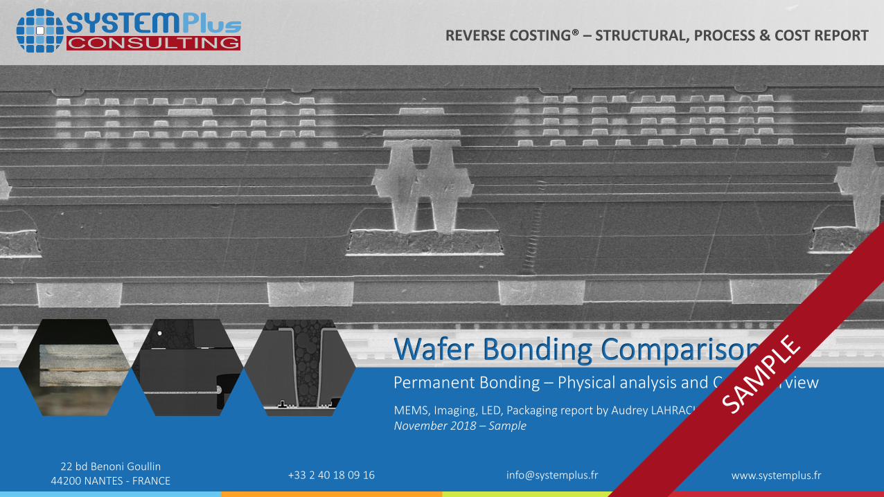
Wafer Bonding ComparisonPermanent Bonding – Physical analysis and Cost Overview
MEMS, Imaging, LED, Packaging report by Audrey LAHRACHNovember 2018 – Sample
REVERSE COSTING® – STRUCTURAL, PROCESS & COST REPORT
©2018 by System Plus Consulting | Wafer to Wafer Permanent Bonding Comparison 2018 2
Table of Contents
Overview / Introduction 5
o Executive Summary
o Reverse Costing Methodology
Permanent Wafer Bonding Technology 9
Permanent Wafer Bonding Definition and Process Description 13
o Without intermediate layer
o Fusion Bonding
o CMOS Image Sensor
o MEMS Inertial Sensor
o Cu-Cu/Oxide Hybrid Bonding
o CMOS Image Sensor
o Anodic Bonding
o MEMS Pressure Sensor
o With intermediate layer
o Glass Frit
o MEMS Pressure Sensor
o MEMS Inertial Sensor
o Adhesive Bonding
o MEMS Micro-mirror
o Eutectic Bonding
o MEMS Inertial Sensor
o Microbolometer
o LED
o Thermo-compression Bonding
o MEMS RF
o MEMS Inertial Sensor
Physical Comparison 140
Cost Comparison 164
Feedbacks 168
SystemPlus Consulting services 170
©2018 by System Plus Consulting | Wafer to Wafer Permanent Bonding Comparison 2018 3
Overview / Introductiono Executive Summaryo Reverse Costing
Methodologyo Glossary
Wafer Bonding Technology
Wafer Bonding Definition and Process Description
Physical Comparison
Cost Comparison
Related Reports
About System Plus
Executive Summary
This comparative review has been conducted to provide insights into the structures, processes and costs of the mainpermanent wafer bonding technologies.
Among these technologies, we have identified two main groups. One, bonding wafers without intermediate layers, includesfusion, copper-copper hybrid and anodic bonding approaches. The second group involves bonding wafers with intermediatelayers using an insulator like a glass frit, or a metal in eutectic and thermocompression approaches. In this report, we showexamples of each wafer bonding approach in different applications. We analyze and compare each wafer bonding process typeto show the benefit in terms of cost and space used.
By switching from glass frit bonding to metal bonding thermo-compression, a manufacturer could reduce component area byup to 30%, reclaiming lost space around the active surface and cutting cost. However, some bonding technologies are currentlyused only in some market segments. For example, hybrid copper-copper bonding is only used in CIS and glass frit technology isfound only in products in automotive and some consumer MEMS applications.
In the comparison, we have analyzed each component’s wafer bonding process, including component dimensions, cost andmanufacturing approach. We provide an overview of technology costs and manufacturer choices by application and range. Weoffer buyers and device manufacturers a unique possibility of understanding permanent wafer bonding technology, evolution,and comparing process costs.
©2018 by System Plus Consulting | Wafer to Wafer Permanent Bonding Comparison 2018 4
Overview / Introduction
Wafer Bonding Technology
Wafer Bonding Definition and Process Description
Physical Comparison
Cost Comparison
Related Reports
About System Plus
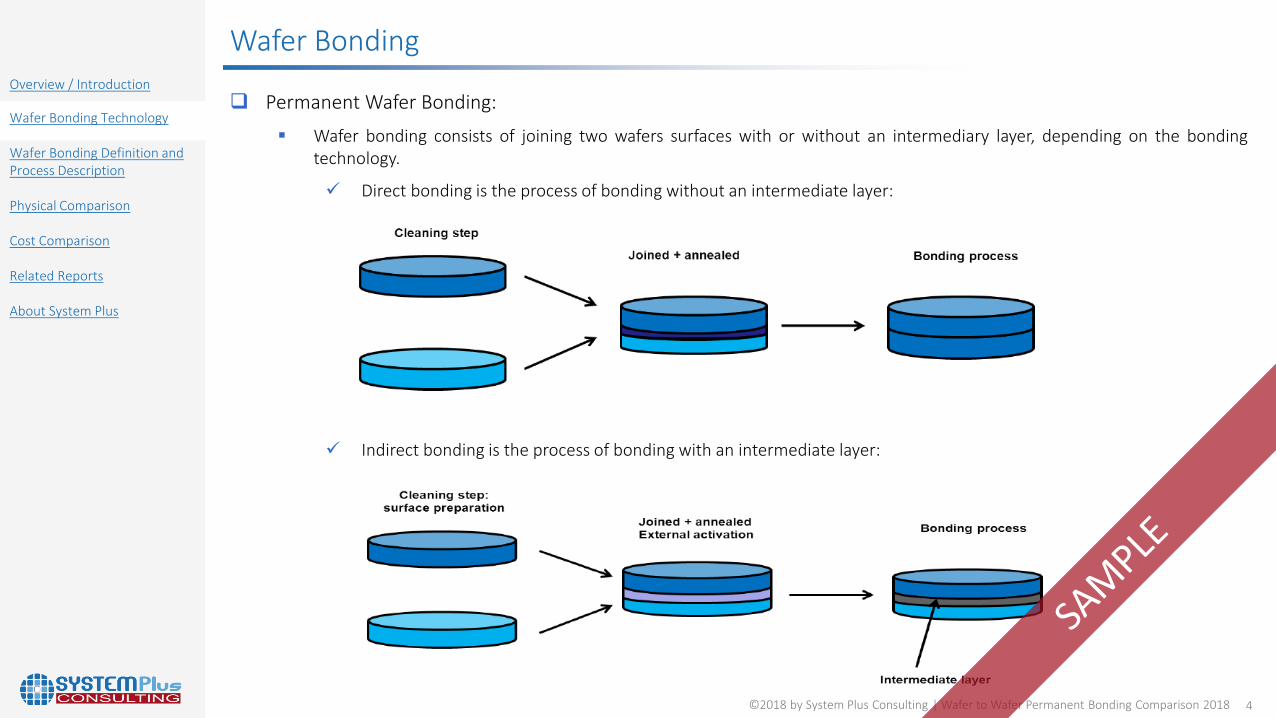
Wafer Bonding
Permanent Wafer Bonding:
Wafer bonding consists of joining two wafers surfaces with or without an intermediary layer, depending on the bondingtechnology.
Direct bonding is the process of bonding without an intermediate layer:
Indirect bonding is the process of bonding with an intermediate layer:
©2018 by System Plus Consulting | Wafer to Wafer Permanent Bonding Comparison 2018 5
Overview / Introduction
Wafer Bonding Technology
Wafer Bonding Definition and Process Description
Physical Comparison
Cost Comparison
Related Reports
About System Plus
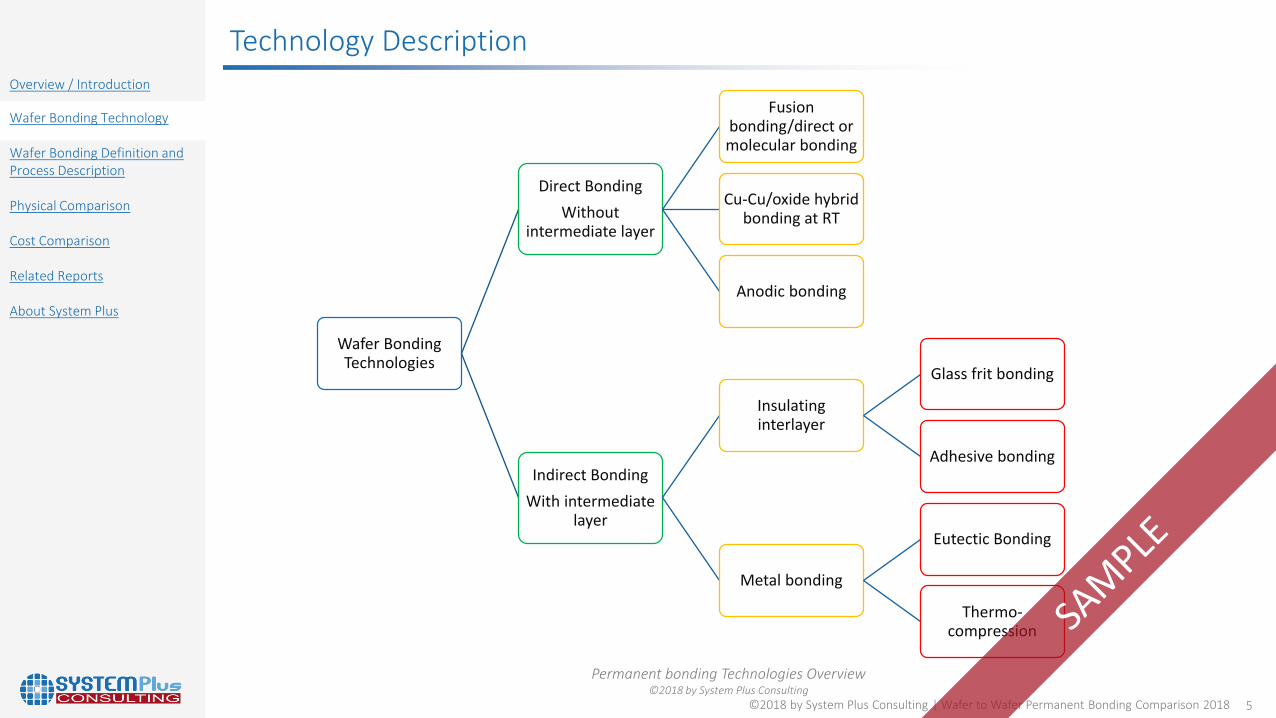
Wafer Bonding Technologies
Direct Bonding
Withoutintermediate layer
Fusion bonding/direct or molecular bonding
Cu-Cu/oxide hybridbonding at RT
Anodic bonding
Indirect Bonding
With intermediatelayer
Insulatinginterlayer
Glass frit bonding
Adhesive bonding
Metal bonding
Eutectic Bonding
Thermo-compression
Technology Description
Permanent bonding Technologies Overview©2018 by System Plus Consulting
©2018 by System Plus Consulting | Wafer to Wafer Permanent Bonding Comparison 2018 6
Overview / Introduction
Wafer Bonding Technology
Wafer Bonding Definition and Process Description
o Without intermediate layero Fusion bondingo Anodic bonding
o With intermediate layero Insulating interlayer
o Glass frit bondingo Adhesive bonding
o Metal Bondingo Cu-Cu/oxide hybrid
bondingo Eutectic Bondingo Thermo-
compression
Physical Comparison
Cost Comparison
Related Reports
About System Plus
Fusion Bonding
©2018 by System Plus Consulting | Wafer to Wafer Permanent Bonding Comparison 2018 7
Overview / Introduction
Wafer Bonding Technology
Wafer Bonding Definition and Process Description
o Without intermediate layero Fusion bondingo Anodic bonding
o With intermediate layero Insulating interlayer
o Glass frit bondingo Adhesive bonding
o Metal Bondingo Cu-Cu/oxide hybrid
bondingo Eutectic Bondingo Thermo-
compression
Physical Comparison
Cost Comparison
Related Reports
About System Plus
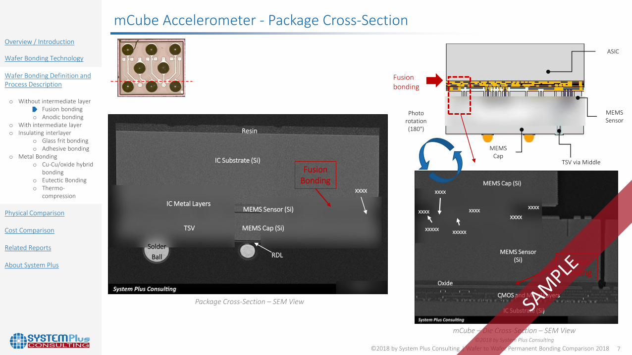
mCube Accelerometer - Package Cross-Section
Package Cross-Section – SEM View
xxxx
IC Substrate (Si)
MEMS Cap (Si)
MEMS Sensor (Si)
Resin
TSV
RDLSolder
Ball
IC Metal Layers
Resin
ASIC
MEMS Sensor
MEMS Cap
TSV via Middle
mCube – Die Cross-Section – SEM View©2018 by System Plus Consulting
xxxxx
MEMS Cap (Si)
xxxxx
MEMS Sensor(Si)
xxxx
xxxxxxxx
IC Substrate (Si)
CMOS and Metal Layers
xxxx
Fusion Bonding
Oxide
xxxx
Photo rotation (180°)
Fusion Bonding
Fusion bonding
©2018 by System Plus Consulting | Wafer to Wafer Permanent Bonding Comparison 2018 8
Overview / Introduction
Wafer Bonding Technology
Wafer Bonding Definition and Process Description
o Without intermediate layero Fusion bondingo Anodic bonding
o With intermediate layero Insulating interlayer
o Glass frit bondingo Adhesive bonding
o Metal Bondingo Cu-Cu/oxide hybrid
bondingo Eutectic Bondingo Thermo-
compression
Physical Comparison
Cost Comparison
Related Reports
About System Plus
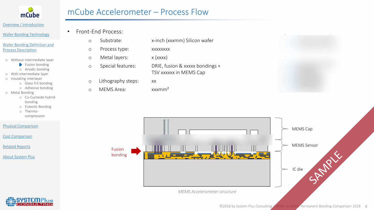
mCube Accelerometer – Process Flow
• Front-End Process:
o Substrate: x-inch (xxxmm) Silicon wafer
o Process type: xxxxxxxx
o Metal layers: x (xxxx)
o Special features: DRIE, fusion & xxxxx bondings + TSV xxxxxx in MEMS Cap
o Lithography steps: xx
o MEMS Area: xxxmm²
MEMS Accelerometer structure
Fusion bonding
TSV
MEMS Sensor
IC die
MEMS Cap
©2018 by System Plus Consulting | Wafer to Wafer Permanent Bonding Comparison 2018 9
Overview / Introduction
Wafer Bonding Technology
Wafer Bonding Definition and Process Description
o Without intermediate layero Fusion bondingo Anodic bonding
o With intermediate layero Insulating interlayer
o Glass frit bondingo Adhesive bonding
o Metal Bondingo Cu-Cu/oxide hybrid
bondingo Eutectic Bondingo Thermo-
compression
Physical Comparison
Cost Comparison
Related Reports
About System Plus
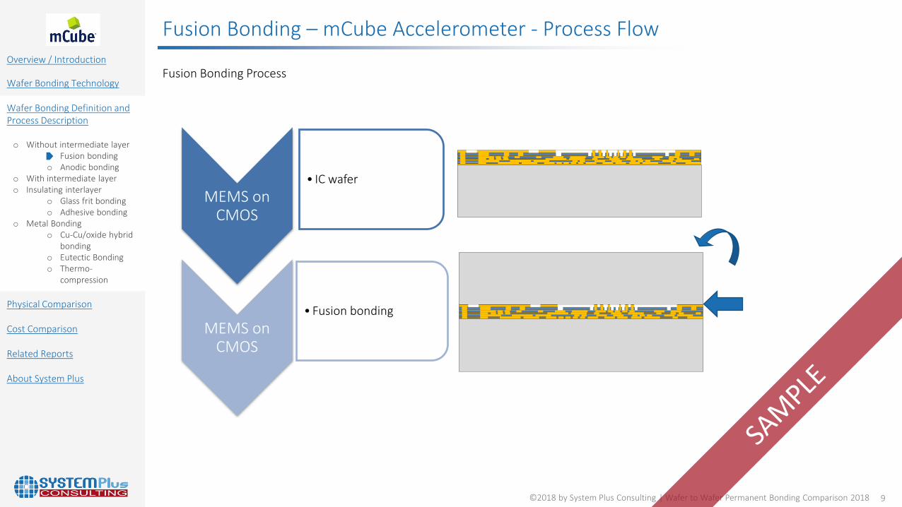
Fusion Bonding – mCube Accelerometer - Process Flow
Fusion Bonding Process
MEMS on CMOS
• IC wafer
MEMS on CMOS
• Fusion bonding
©2018 by System Plus Consulting | Wafer to Wafer Permanent Bonding Comparison 2018 10
P H Y S I C A LCOMPARISON
©2018 by System Plus Consulting | Wafer to Wafer Permanent Bonding Comparison 2018 11
Overview / Introduction
Wafer Bonding Technology
Wafer Bonding Definition and Process Description
Physical Comparison
Cost Comparison
Related Reports
About System Plus
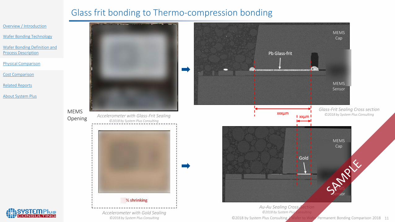
Glass frit bonding to Thermo-compression bonding
Pb Glass-frit
MEMS Cap
MEMS Sensor
Gold
MEMS Cap
MEMS Sensor
xxxµmxxµm
Au-Au Sealing Cross-Section©2018 by System Plus ConsultingAccelerometer with Gold Sealing
©2018 by System Plus Consulting
Accelerometer with Glass-Frit Sealing©2018 by System Plus Consulting
Glass-Frit Sealing Cross section©2018 by System Plus Consulting
MEMS Opening
©2018 by System Plus Consulting | Wafer to Wafer Permanent Bonding Comparison 2018 12
Overview / Introduction
Wafer Bonding Technology
Wafer Bonding Definition and Process Description
Physical Comparison
Cost Comparison
Related Reports
About System Plus
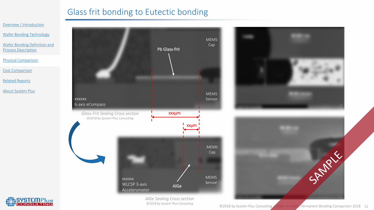
Glass frit bonding to Eutectic bonding
xxxµm
Pb Glass-frit
MEMS Cap
MEMS Sensor
xxµm
AlGe
MEMS Cap
MEMS Sensor
Glass-Frit Sealing Cross section©2018 by System Plus Consulting
AlGe Sealing Cross section©2018 by System Plus Consulting
xxxxxxWLCSP 3-axis Accelerometer
xxxxxx6-axis eCompass
©2018 by System Plus Consulting | Wafer to Wafer Permanent Bonding Comparison 2018 13
C O S TCOMPARISON
©2018 by System Plus Consulting | Wafer to Wafer Permanent Bonding Comparison 2018 14
Overview / Introduction
Wafer Bonding Technology
Wafer Bonding Definition and Process Description
Physical Comparison
Cost Comparison
Related Reports
About System Plus
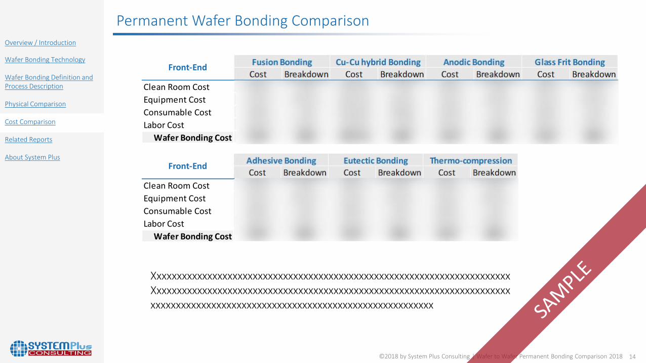
Permanent Wafer Bonding Comparison
Clean Room Cost
Equipment Cost
Consumable Cost
Labor Cost
Wafer Bonding Cost
Front-End
Clean Room Cost
Equipment Cost
Consumable Cost
Labor Cost
Wafer Bonding Cost
Front-End
XxxxxxxxxxxxxxxxxxxxxxxxxxxxxxxxxxxxxxxxxxxxxxxxxxxxxxxxxxxxxxxxxxxxxxxXxxxxxxxxxxxxxxxxxxxxxxxxxxxxxxxxxxxxxxxxxxxxxxxxxxxxxxxxxxxxxxxxxxxxxxxxxxxxxxxxxxxxxxxxxxxxxxxxxxxxxxxxxxxxxxxxxxxxxxxxxxxxxx
©2018 by System Plus Consulting | Wafer to Wafer Permanent Bonding Comparison 2018 15
Overview / Introduction
Wafer Bonding Technology
Wafer Bonding Definition and Process Description
Physical Comparison
Cost Comparison
Related Reports
About System Plus
Related Reports
MARKET AND TECHNOLOGY REPORTS - YOLE DÉVELOPPEMENTREVERSE COSTING ANALYSES - SYSTEM PLUS CONSULTING
PACKAGING• MEMS Packaging: Reverse Technology Review• MEMS Pressure Sensor Comparison 2018
MARKET AND TECHNOLOGY REPORTS - YOLE DÉVELOPPEMENT
ADVANCED PACKAGING• Bonding and Lithography Equipment Market for More than Moore
Devices• Status of the MEMS Industry 2018• Equipment and Materials for 3D TSV Applications 2017• Status of the CMOS Image Sensor Industry 2018• MEMS Packaging 2017
©2018 by System Plus Consulting | Wafer to Wafer Permanent Bonding Comparison 2018 16
Overview / Introduction
Wafer Bonding Technology
Wafer Bonding Definition and Process Description
Physical Comparison
Cost Comparison
Related Reports
About System Plus
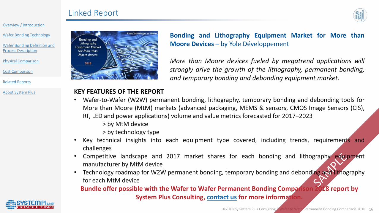
Linked Report
Bonding and Lithography Equipment Market for More thanMoore Devices – by Yole Développement
More than Moore devices fueled by megatrend applications willstrongly drive the growth of the lithography, permanent bonding,and temporary bonding and debonding equipment market.
KEY FEATURES OF THE REPORT• Wafer-to-Wafer (W2W) permanent bonding, lithography, temporary bonding and debonding tools for
More than Moore (MtM) markets (advanced packaging, MEMS & sensors, CMOS Image Sensors (CIS),RF, LED and power applications) volume and value metrics forecasted for 2017–2023
> by MtM device> by technology type
• Key technical insights into each equipment type covered, including trends, requirements andchallenges
• Competitive landscape and 2017 market shares for each bonding and lithography equipmentmanufacturer by MtM device
• Technology roadmap for W2W permanent bonding, temporary bonding and debonding and lithographyfor each MtM device
Bundle offer possible with the Wafer to Wafer Permanent Bonding Comparison 2018 report by System Plus Consulting, contact us for more information.
©2018 by System Plus Consulting | Wafer to Wafer Permanent Bonding Comparison 2018 17
SystemPlusConsultingSERVI CES
©2018 by System Plus Consulting | Wafer to Wafer Permanent Bonding Comparison 2018 18
Overview / Introduction
Wafer Bonding Technology
Wafer Bonding Definition and Process Description
Physical Comparison
Cost Comparison
Related Reports
About System Pluso Company serviceso Contact
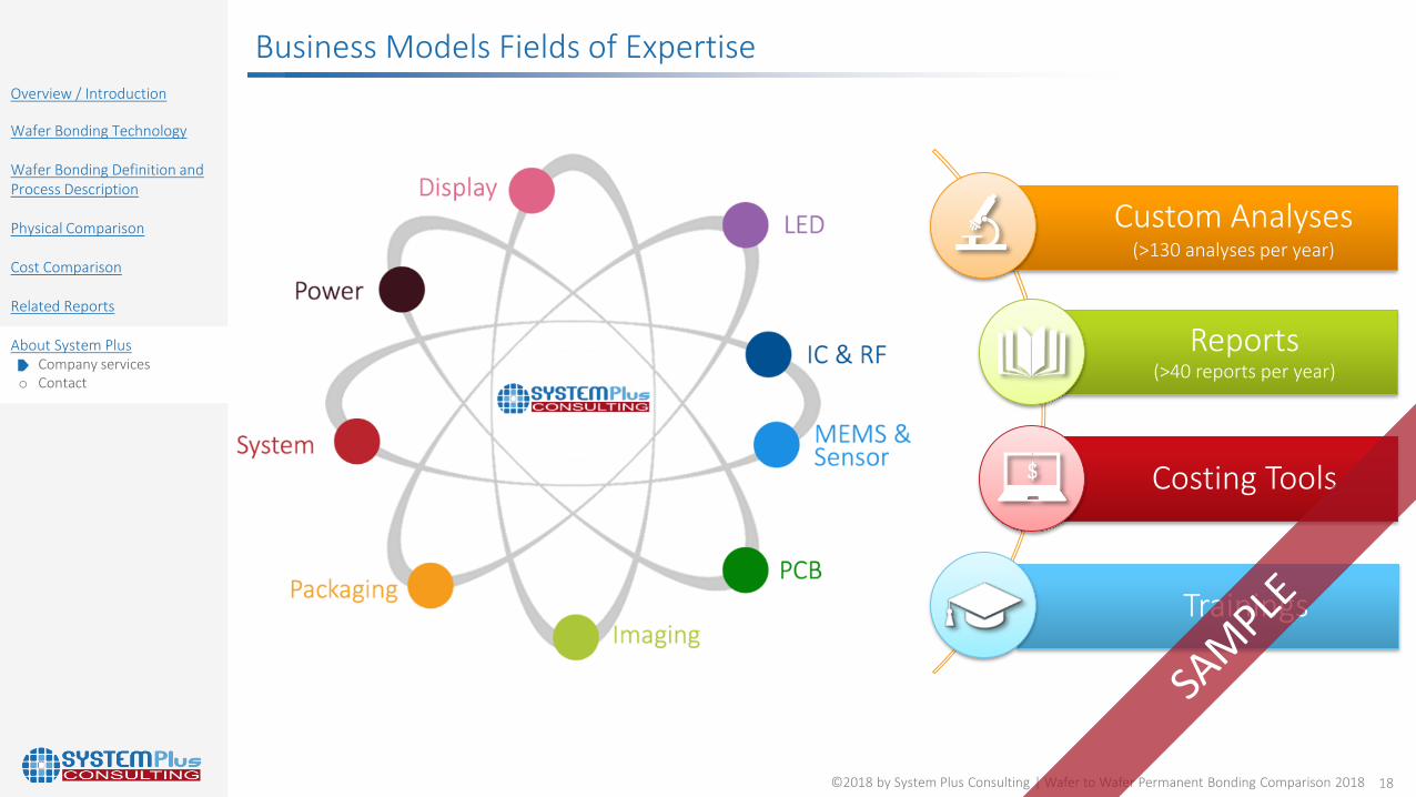
Business Models Fields of Expertise
Custom Analyses(>130 analyses per year)
Reports(>40 reports per year)
Costing Tools
Trainings
©2018 by System Plus Consulting | Wafer to Wafer Permanent Bonding Comparison 2018 19
Overview / Introduction
Wafer Bonding Technology
Wafer Bonding Definition and Process Description
Physical Comparison
Cost Comparison
Related Reports
About System Pluso Company serviceso Contact
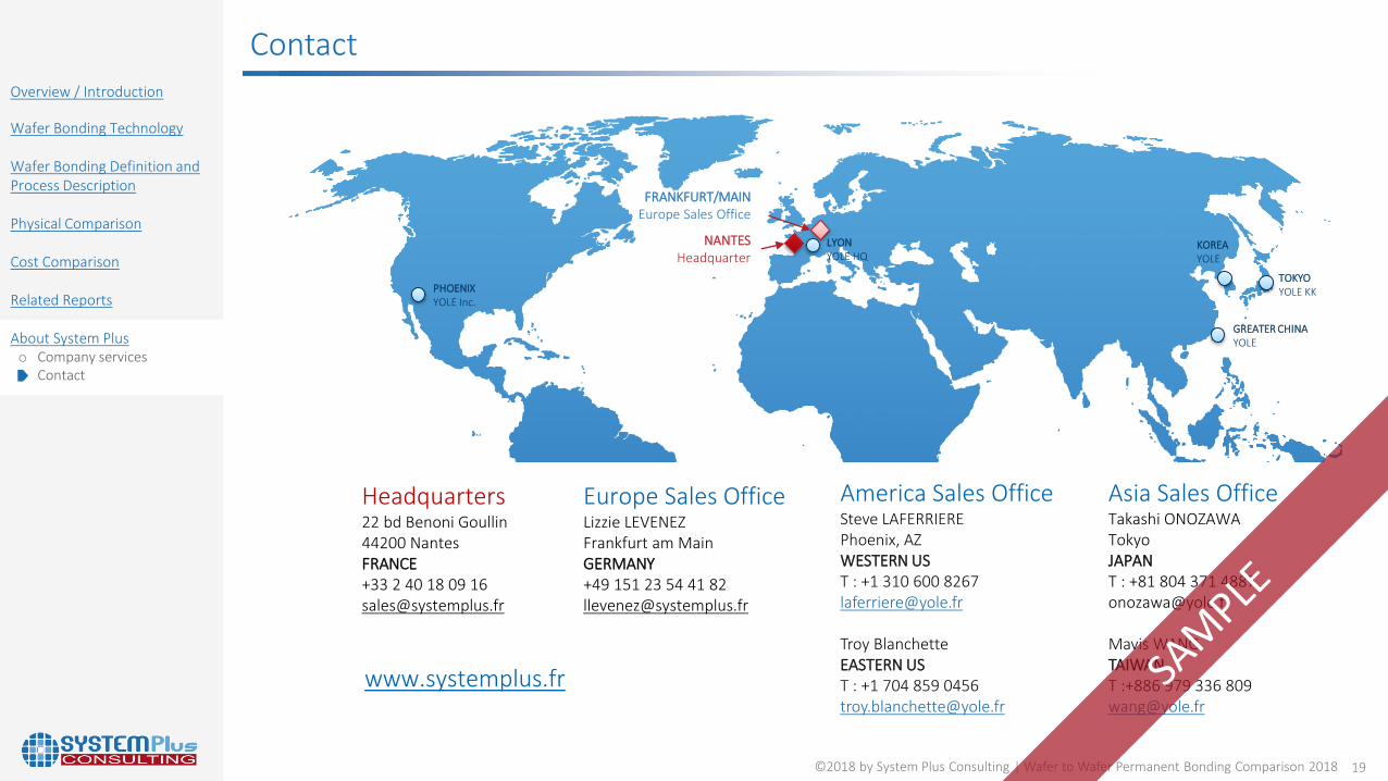
Contact
Headquarters22 bd Benoni Goullin44200 NantesFRANCE+33 2 40 18 09 [email protected]
Europe Sales OfficeLizzie LEVENEZFrankfurt am MainGERMANY+49 151 23 54 41 [email protected]
America Sales OfficeSteve LAFERRIEREPhoenix, AZWESTERN UST : +1 310 600 [email protected]
Troy BlanchetteEASTERN UST : +1 704 859 [email protected]
www.systemplus.fr
Asia Sales OfficeTakashi ONOZAWATokyoJAPANT : +81 804 371 [email protected]
Mavis WANGTAIWANT :+886 979 336 [email protected]
NANTESHeadquarter
FRANKFURT/MAINEurope Sales Office
LYONYOLE HQ
TOKYOYOLE KK
GREATER CHINAYOLE
PHOENIXYOLE Inc.
KOREAYOLE
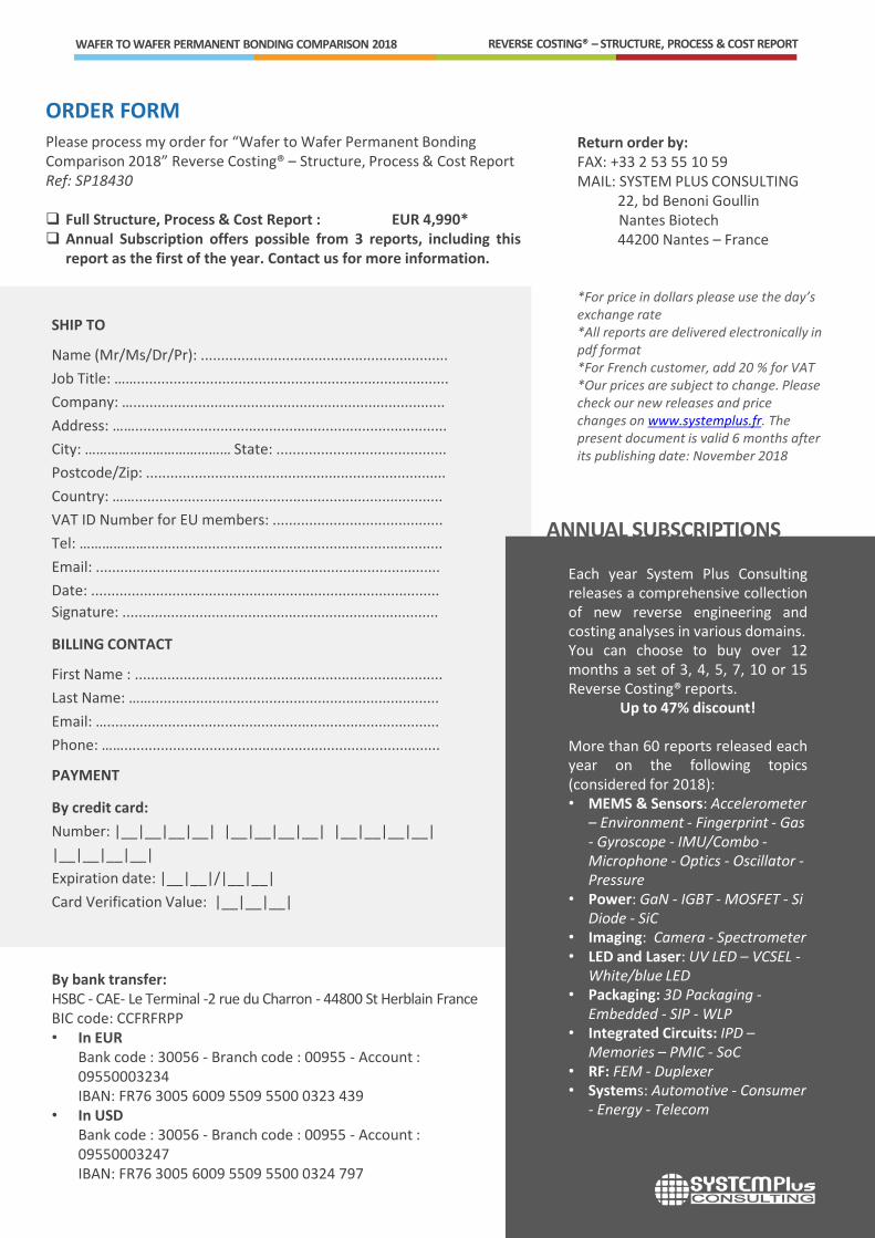
ORDER FORMPlease process my order for “Wafer to Wafer Permanent Bonding Comparison 2018” Reverse Costing® – Structure, Process & Cost Report Ref: SP18430
Full Structure, Process & Cost Report : EUR 4,990* Annual Subscription offers possible from 3 reports, including this
report as the first of the year. Contact us for more information.
SHIP TO
Name (Mr/Ms/Dr/Pr): .............................................................
Job Title: …….............................................................................
Company: ….............................................................................
Address: …….............................................................................
City: ………………………………… State: ..........................................
Postcode/Zip: ..........................................................................
Country: ……............................................................................
VAT ID Number for EU members: ..........................................
Tel: ……………….........................................................................
Email: .....................................................................................
Date: ......................................................................................
Signature: ..............................................................................
BILLING CONTACT
First Name : ............................................................................
Last Name: …….......................................................................
Email: …..................................................................................
Phone: ……..............................................................................
PAYMENT
By credit card:
Number: |__|__|__|__| |__|__|__|__| |__|__|__|__|
|__|__|__|__|
Expiration date: |__|__|/|__|__|
Card Verification Value: |__|__|__|
By bank transfer:HSBC - CAE- Le Terminal -2 rue du Charron - 44800 St Herblain FranceBIC code: CCFRFRPP• In EUR
Bank code : 30056 - Branch code : 00955 - Account : 09550003234 IBAN: FR76 3005 6009 5509 5500 0323 439
• In USDBank code : 30056 - Branch code : 00955 - Account : 09550003247 IBAN: FR76 3005 6009 5509 5500 0324 797
Return order by: FAX: +33 2 53 55 10 59MAIL: SYSTEM PLUS CONSULTING
22, bd Benoni GoullinNantes Biotech44200 Nantes – France
*For price in dollars please use the day’s exchange rate *All reports are delivered electronically in pdf format*For French customer, add 20 % for VAT*Our prices are subject to change. Please check our new releases and price changes on www.systemplus.fr. The present document is valid 6 months after its publishing date: November 2018
REVERSE COSTING® – STRUCTURE, PROCESS & COST REPORTWAFER TO WAFER PERMANENT BONDING COMPARISON 2018
Each year System Plus Consultingreleases a comprehensive collectionof new reverse engineering andcosting analyses in various domains.You can choose to buy over 12months a set of 3, 4, 5, 7, 10 or 15Reverse Costing® reports.
Up to 47% discount!
More than 60 reports released eachyear on the following topics(considered for 2018):• MEMS & Sensors: Accelerometer
– Environment - Fingerprint - Gas - Gyroscope - IMU/Combo -Microphone - Optics - Oscillator -Pressure
• Power: GaN - IGBT - MOSFET - Si Diode - SiC
• Imaging: Camera - Spectrometer• LED and Laser: UV LED – VCSEL -
White/blue LED• Packaging: 3D Packaging -
Embedded - SIP - WLP• Integrated Circuits: IPD –
Memories – PMIC - SoC• RF: FEM - Duplexer• Systems: Automotive - Consumer
- Energy - Telecom
ANNUAL SUBSCRIPTIONS
1.INTRODUCTIONThe present terms and conditions apply to the offers, sales and deliveries of services managed by System PlusConsulting except in the case of a particular written agreement.Buyer must note that placing an order means an agreement without any restriction with these terms and conditions.
2.PRICESPrices of the purchased services are those which are in force on the date the order is placed. Prices are in Euros andworked out without taxes. Consequently, the taxes and possible added costs agreed when the order is placed will becharged on these initial prices.System Plus Consulting may change its prices whenever the company thinks it necessary. However, the companycommits itself in invoicing at the prices in force on the date the order is placed.
3.REBATES and DISCOUNTSThe quoted prices already include the rebates and discounts that System Plus Consulting could have granted accordingto the number of orders placed by the Buyer, or other specific conditions. No discount is granted in case of earlypayment.
4.TERMS OF PAYMENTSystem Plus Consulting delivered services are to be paid within 30 days end of month by bank transfer except in thecase of a particular written agreement.If the payment does not reach System Plus Consulting on the deadline, the Buyer has to pay System Plus Consulting apenalty for late payment the amount of which is three times the legal interest rate. The legal interest rate is thecurrent one on the delivery date. This penalty is worked out on the unpaid invoice amount, starting from the invoicedeadline. This penalty is sent without previous notice.When payment terms are over 30 days end of month, the Buyer has to pay a deposit which amount is 10% of the
total invoice amount when placing his order.
5. OWNERSHIPSystem Plus Consulting remains sole owner of the delivered services until total payment of the invoice.
6.DELIVERIESThe delivery schedule on the purchase order is given for information only and cannot be strictly guaranteed.Consequently any reasonable delay in the delivery of services will not allow the buyer to claim for damages or tocancel the order.
7.ENTRUSTED GOODS SHIPMENTThe transport costs and risks are fully born by the Buyer. Should the customer wish to ensure the goods against lost ordamage on the base of their real value, he must imperatively point it out to System Plus Consulting when theshipment takes place. Without any specific requirement, insurance terms for the return of goods will be the carriercurrent ones (reimbursement based on good weight instead of the real value).
8.FORCE MAJEURESystem Plus Consulting responsibility will not be involved in non execution or late delivery of one of its dutiesdescribed in the current terms and conditions if these are the result of a force majeure case. Therefore, the forcemajeure includes all external event unpredictable and irresistible as defined by the article 1148 of the French CodeCivil?
9.CONFIDENTIALITYAs a rule, all information handed by customers to system Plus Consulting are considered as strictly confidential.A non-disclosure agreement can be signed on demand.
10.RESPONSABILITY LIMITATIONThe Buyer is responsible for the use and interpretations he makes of the reports delivered by System Plus Consulting.Consequently, System Plus Consulting responsibility can in no case be called into question for any direct or indirectdamage, financial or otherwise, that may result from the use of the results of our analysis or results obtained usingone of our costing tools.
11.APPLICABLE LAWAny dispute that may arise about the interpretation or execution of the current terms and conditions shall be resolvedapplying the French law.It the dispute cannot be settled out-of-court, the competent Court will be the Tribunal de Commerce de Nantes.
TERMS AND CONDITIONS OF SALES