Embed Size (px)
Citation preview

Volume III, Issue V, May 2014 IJLTEMAS ISSN 2278 - 2540
www.ijltemas.in Page 129
Preparation of Cu2O and CuO Nano Layerson ITO
Coated Glass Substrate
Using Single Precursor Solution
K. Amudhavalli
Department of Physics, VOC College, Thoothukudi, India
N. Neelakandapillai
Department of Physics, Arignar Anna College,
Aralvoimozhi, India
Abstract- Copper oxide is a fascinating material because of its
applications in many fields. In the present work both cuprous
and cupric oxides nano thin films were electrochemically
deposited on ITO coated glass substrate using a single solution
precursor in an alkaline medium. The effects of potential on
the crystal size and band gap values were analysed. Structural
characteristics of the films were investigated by X- ray
diffraction analysis (XRD). From the XRD graph the crystal
size and lattice parameters were calculated. UV-Vis
Absorbance spectra and Transmittance spectra were recorded
using JASCO V-530 model Spectrophotometer to calculate the
optical band gap values. The surface morphology was studied
using SEM image.
Key words- CuO, Cu2O, Anodic deposition, Cathodic deposition,
Deby- Scherrer’s formula, Band gap.
I. INTRODUCTION
esearchers across the world have been already engaged
in preparing Cuprous and Cupric oxides for various
applications using different techniques and a few are
thermal oxidation, reactive sputtering, spraying, plasma
evaporation, molecular beam epitaxy, chemical solution
deposition, elctrodeposition etc.
Balamurugan et al. [1] prepared copper oxide by
reactive evaporation method and studied its optical and
structural properties. Samarasekara [2] prepared Cu2O and
CuO thin layer on ITO coated glass substrate and studied
the optical properties of the prepared films. Takeshi et al.
[3] fabricated Cu2O film by electro deposition method.
Musa et al. [4] produced cuprous oxide by thermal oxidation
and studied its physical and electrical properties.
Mahalingam et al. [5] deposited cuprous oxide thin films by
cathodic reduction of copper (II) lactate solution. Nakaoka
et al. [6] studied the photoelectrochemical behaviour of
Cu2O and CuO thin films electrodeposited on ITO coated
glass substrate.
Cupric oxide has been prepared by many a
researcher using various methods. Li, J., et al. [7], Siripala
et al.[8], Ozawa et al. [9]prepared CuO bythermal oxidation.
Nahle et al. [10], and,Yoon et al.[11] synthesised CuO by
ion beam sputtering and studied its photoelectrochemical
behaviour. Philippe Poizot et al. [12] prepared Cu2O and
CuO thin films by cathodic and anodic electrodeposition in
an alkaline medium.
After having reviewed the methods and techniques
cited the present researcher introduces a new
electrochemical method to deposit well-crystallized cuprous
and cupric oxide from a single soluble Cu(II) precursor.
The two well-known oxides of Copper are cuprite
(Cu2O) and tenorite (CuO). But the physical properties,
colours, crystal nature and electrical properties of both are
different. They are non-toxic source materials and the
method of preparation of these oxides would be cost
effective. It has been widely used as they have good
electrical and optical properties. Both CuO and Cu2O
materials are known to be p-type semiconductors in general
and hence potentially useful for constructing junction
devices such as p-n junction diodes.
Cu2O is naturally a p-type semiconductor and has a
simple cubic structure which belongs to the space group p-
n-3m. Its band gap value is from 1.9 eV to 2.2ev.and lattice
constant is 4.27 A0 [1]. The stoichiometry is 2:1. Depending
on the size it is yellow or red in colour. Its density is 6.0
g/cm3. It has a high melting point of 1235 ºC and does not
dissolve in water. Cu2O exhibits n-type and p-type
depending on the pH of the solution [5].
CuO has a unique monoclinic structure with a
space group of C2/c. CuO is a p-type semiconductor and its
band gap energy is ranging between 1.21 and 1.51 eV [13].
The lattice parameters of CuO are a=4.6837 A0, b=3.4226
A0, c= 5.1288 A
0 and β=99.54. Since it is a p-type
semiconducting material conduction arises from the holes
present in the valence band due to doping/annealing [14]. It
is a selective solar cell absorber. It has high solar
absorbance and low thermal emittance [15]. Pure cupric
oxide is a black solid with a density of 6.31 g/cm3. It also
has a high melting point of 1330 ºC and is insoluble in
R

Volume III, Issue V, May 2014 IJLTEMAS ISSN 2278 - 2540
www.ijltemas.in Page 130
water. Due to the crystallinity and higher transparency CuO
films are suitable for optical analysis.
Indium Oxide heavily doped with Tin (ITO) coated
glass plate is selected as a substrate to coat CuO and Cu2O
thin films. Indium tin oxide is one of the most widely used
transparent conducting oxides because of its optical
properties. ITO has been widely studied in the past three
decades due to its special properties as a semiconductor.
The ITO electrode consists of indium (III) oxide (In2O3)
and tin (IV) oxide (SnO2), with typically 90% In2O3 and
10% SnO2 by weight. It has a high transmittance in the
visible light range and also has an outstanding electrical
conductivity. Also, it has been used as a transparent contact
in advanced electronic devices like Solar cells, Light
Emitting Diode, Photodiode, Phototransistor and Laser. Its
high transparency is used to check the type n/p of the films
to be deposited on it. It is used to improve the optical
sensitivity of light detecting devices. The direct optical band
gap of ITO film is generally greater than 3.75 eV [16] but a
range of values from 3.5 eV to 4.06 eV is reported in the
literature [17].
Though different methods were adopted to prepare
both cuprous and cupric oxide, the electro chemical
deposition is an attractive method for the synthesis of thin
films [8], [18], [5],[19] and [20]. The advantages of using
this are low cost, low processing temperature,
normalhandling pressure, high purity of deposition, large
area deposition and controlled thickness of the film. Both
Cu2O and CuO thin films were prepared using this
technique.
II. METHODS AND MATERIALS
Regulated DC power supply with 3 electrodes
system is used to deposit the films. It consists of a working
electrode, a counter electrode and a reference electrode.
A. Preparation of working electrode
Both cuprous and cupric oxides were coated on the
working electrode. The working electrode is ITO coated
glass substrate plate of 20mmX20mmX1.1mm with a sheet
resistance of 10 ohms/sq. For experimental purpose the
plates are cut into 1cmX 2cm strips. Before deposition the
surface of the working electrodes are well cleaned by
acetone, soap water and then ultrasonicated for 30 minutes
using sonicator bath. Then the plate is rinsed with double
distilled water and allowed to dry completely.
B. Preparation of the Counter Electrode
The counter electrode is a platinum electrode. A
platinum sheet in 3mmX 3mm size is well polished and is
enclosed by a glass tube. Current will flow between the
working electrode and the counter electrode.
C. Preparation of the Reference Electrode
The reference electrode is a saturated calamel
electrode (SCE). The electrode is filled with a saturated KCl
solution. Since the reference electrode has a constant make
up, its potential is fixed. Therefore it is well used to control
the potential of the working electrode.
D. Preparation of Electrolyte
This paper introduces a new electrochemical
method to deposit well-crystallized cuprous and cupric
oxides from a single soluble Cu(II) precursor. Copper
Sulphate Pentahydrate (CuSO4.5HO) is used as a copper
source. Tartaric acid (CHOHCOOH) is used as a chelating
agent, which has -CH(OH)COOH group, and is effective to
form crystalline Cu2O and CuO. Sodium hydroxide (NaOH)
is used to adjust the pH of the solution. All the chemicals
are Analar Grade Reagents with 99% purity and purchased
form Merck. The electrolyte is prepared with 0.1M of
Copper Sulphate Pentahydrate pure and 0.1M of tartaric
acid. Solution of 1M of NaOH is prepared and is used to
adjust the pH of the electrolyte. An equal volume of copper
sulphate solution and tartaric acid solution are mixed and
the pH of the solution is maintained at 11 and 13 to form
Cu2O and CuO respectively. Prior to the deposition, the bath
temperature and the time of deposition are optimised. The
temperature of the bath is maintained at room temperature
for slow deposition. The films are deposited for 1 hour.
Electrochemical work station CHI-650C (CH
Instruments, USA) is employed for electrochemical and
electro analysis studies. The deposition mechanism is
investigated using cyclic voltammetry. The appropriate
potential region in which the formation of stoichiometric
Cu2O and CuO thin films occurs is found to be between -
800 mV and +600 mV. Cu2O is prepared cathodically, and
using the same solution CuO is prepared anodically. For the
preparation of Cu2O thin film on ITO coated glass plate the
potential value from -0.50V, -0.53V, -0.58V, Vs SCE is
applied and to grow CuO thin layer, the potential value is
varied from 0.45V , 0.50V and 0.55V Vs SCE .
Earlier studies on CuO thin films show that CuO
formation is possible either due to local pH decrease near
the electrode surface or oxidation of Cu(II) to a metastable
Cu(III) species followed by chemical decomposition of the
oxidised species. But Poizot’s experiment reveals that CuO
precipitation is possible by electrochemical destruction of
the soluble copper complexes. And, though alkaline Cu(II)-
tartrate solution is not a common bath for the cathodic
deposition of Cu2O, Cu2O is grown successfully on ITO
coated glass substrate by cathodic deposition in the present
work. The formation of Cu2 O and CuO is given below:
CuSO4 Cu2+
+ SO42-
Cu2+.
T T* + ne
- + Cuaq
2+
Cuaq2+
+2 OH- Cu(OH)2 CuO + H2 O
2Cu2+
+ 2e-
+ 2OH- Cu 2O + H2 O

Volume III, Issue V, May 2014 IJLTEMAS ISSN 2278 - 2540
www.ijltemas.in Page 131
where T is tartrate ion, T* oxidized tartrate ion, and Cu2+.
T
represents a Cu(II)-tartrate complex. Cu2O is formed when
the potential to the substrate is negative. And, when the
potential is positive tartaric ions are oxidised and Cu2+
T is
broken. This produces precipitation of Cu2+
ions and forms
CuO. The solution pH is maintained at pH= 11 for cathodic
deposition of Cu2O and three samples are prepared for the
potential values -0.45V, -0.50V and -0.55V. For anodic
deposition of CuO the solution pH is maintained at pH=13
and three samples are coated for potentials 0.50V, 0.53V
and 0.58V.
After the deposition, the samples were washed with
distilled water and dried at room temperature.
III. RESULTS AND DISCUSSION
The thin films were characterized by various
instrumental techniques.
XRD measurements were made using XPERT-
PRODiffractometer with CuKα (λ=1.54) radiation at 40 kV
and 30mA with a scanning rate of 100/min and the scan
range was from 2θ=100 to 90
0 to identify the crystal
structure of the film. The optical property were studied
using JASCO V530 model UV –Vis
Spectrophotometer.The surface morphology is analysed
using scanning electron microscopy (SEM).
The XRD measurements were taken for the Cu2O
films depositied at -0.50V, -0.53V,-0.58V at room
temperature. The diffraction peaks observed in the XRD
spectrum were indexed (Fig.1). The diffraction peaks
appearing around 36.4, 42.3, 61.3and 73.5 correspond to
(111), (200), (220) and (311) planes of Cubic Cu2O
respectively, accoding to JCPDS card No. 05-0667. The
presence of several peaks shows that the Cu2O grown is of
polycrystalline. But the strongest peak appears at 36.4
which indicates that the prefered orientation is (111) plane.
The lattice constant for Cu2O is a=0.4267nm which agrees
well with the standard value a=0.4258nm(JCPDS card No.
05-0667).
Similarly the XRD measurements for
anodicallycoatedCuO films deposited at potentials 0.45V,
0.50V and 0.55V were taken(Fig. 2). For all the potential
values the preferred orientation is (002) plane and is seen in
the XRD spectrum at 2θ=35.270. But as deposition potential
increases at 0.50V and 0.55V a peak appears at 2θ=66.30
which corresponds to (-311) plane. The lattice parameter
values for CuO are calculated as a = 4.6988 A0,
10 20 30 40 50 60 70 800
1000
2000
(311)
(311)
(311)
(110)
*
*
(200)
(200)
(200)
(220)
(220)
*
*
*
*
*
*
*
*
Inte
nsity (
a.u
)
2
0.58V
0.53V
0.50V
Cu2O (111)
(110)
*
(220)*
Fig. 1 X-ray diffraction patterns of Cu2O thin film deposited at potent
a) -0.50V b) -0.53V and c) -0.58V Vs SCE.
b = 3.5197 A0 and c= 5.162 A
0 and this is in good agreement
with thestandard values ( a = 4.6837 A0, b=3.4226 A
0, c=
5.1288 A0). The grain size of the thin film is estimated from
Debye Scherrer’s formula
D =𝟎.𝟗𝟒𝛌
𝜷 𝒄𝒐𝒔𝜽
where β is the full–width at half maximum (FWHM) of a
Bragg peak, λ the X-ray wavelength (=1.5406 nm) and 𝜃 the
Bragg angle. For prominent peaks the sizes of the particles
are estimated. For Cu2O film the calculated particle sizes
are 73nm, 70nm and 45nm for the potentials -0.50V, -0.53V
and -0.58V Vs SCE respectively. This shows that the grain
size decreases as deposition potential is more negative. The
XRD graph clearly shows that as deposition potential is
increased the width of the peak broadens and shows the
decrease of the grain size. WilmanSeptina [21] observed the
same result. When the applied potential is more negative the
crystal size decreases becausethe frequencies ofnucleation
of Cu2O crystals may behigher atmore

Volume III, Issue V, May 2014 IJLTEMAS ISSN 2278 - 2540
www.ijltemas.in Page 132
10 20 30 40 50 60 70 80 90
500
1000
1500
a
b
0.45V
0.50V
0.55V
(-202)(111)
(002)
(002)
ITO
ITO
ITO
(311)
(-202)
ITO
ITO
ITO
ITO
ITO
C
ou
nts
(a
.u)
2
ITO
(111)
(311)
(002)
CuO Anodic deposition
c
Fig. 2 X-ray diffraction patterns of CuO thin films deposited at potentials a) -0.45V b) -0.50V and c) -0.55V Vs SCE.
negativepotential. Similarly for CuO films the particle sizes
are 39nm 34nm and 33nm for the potential values 0.45V
,0.50V and 0.55V respectively and the size is found to
decrease as the potential increases.
UV- VIS absorbance spectra were recorded using
JASCO V-530 model Spectrophotometer. The optical
absorption spectra were taken for all the samples with
respect to the substrate ITO coated glass plates in the range
300 nm to 1100 nm. The spectra of both CuO and Cu2O
were analysed by plotting ℎ 𝛾 verses (α ℎ 𝛾 )^n.
(∝ ℎ 𝛾)^𝑛 = 𝐴(ℎ 𝛾 − 𝐸𝑔)
where A is a constant and n depends on the nature of the
transition processes; n= ½ is for indirect allowed transition,
n =2 is for direct allowed transition and n =2/3 is for
forbidden direct allowed transition and n=1/3 represents
indirect forbidden transition. Linear plot is obtained when
n=2 for all Cu2O films (Fig. 3a, Fig 3b, Fig 3c). This shows
that the film deposited is of direct allowed transition. But
for CuO linear relation is obtained while
1.2 1.4 1.6 1.8 2.0 2.2 2.4 2.6 2.8 3.0 3.20
10
20
30
40
(
h)^
2 X
10
8 c
m-2
h
Cu2O 0.50V
Fig. 3a Tauc plot between energy vs (αhν)^2 for Cu2O films deposited at
potential -0.50V Vs SCE
1.2 1.4 1.6 1.8 2.0 2.2 2.4 2.6 2.8 3.0 3.20
20
40
60
80
100
120
140
160
(
h)^
2x
10
8c
m-2
h
Cu2O 0.53V
Fig. 3 bTauc plot between energy Vs (αhν)^2 for Cu2O films deposited at
potential -0.53V Vs SCE.

Volume III, Issue V, May 2014 IJLTEMAS ISSN 2278 - 2540
www.ijltemas.in Page 133
1.0 1.2 1.4 1.6 1.8 2.0 2.2 2.4 2.6 2.8 3.0
0
5
10
15(
h)^
2x
10
8c
m-2
h
Cu2O -0.58V
Fig. 3 c Tauc plot between energy vs (αhν)^2 for Cu2O films deposited at
potential -0.58V Vs SCE.
1.0 1.2 1.4 1.6 1.8 2.0 2.2 2.4 2.6 2.8 3.00
1
2
3
(
h)^
0.5
x1
08
cm
-2e
V2
h(eV)
CuO 0.45V
Fig. 4 a Tauc plot between energy Vs (αhν)1/2 for CuO films deposited at potential -0.45V Vs SCE.
1.0 1.2 1.4 1.6 1.8 2.0 2.2 2.4 2.6 2.8 3.00
5
(
h)^
0.5
x1
08c
m-2e
V2
h(eV)
CuO 0.50V
Fig. 4 b Tauc plot between energy vs (αhν)1/2 for CuO films deposited at potential -0.50V Vs SCE.
n=1/2. This predicts that the deposited CuO film is an
indirect band gap type. From the intercepts of the straight
line on the X-axis the band gap values are calculated. The
band gap value thus obtained is in the range 1.7 eV to 2.35
eV for Cu2O and 1.3 eV to 1,55eV for CuO thin films. This
is in good agreement with the standard values(Fig.4a, Fig.
4b,Fig. 4c).
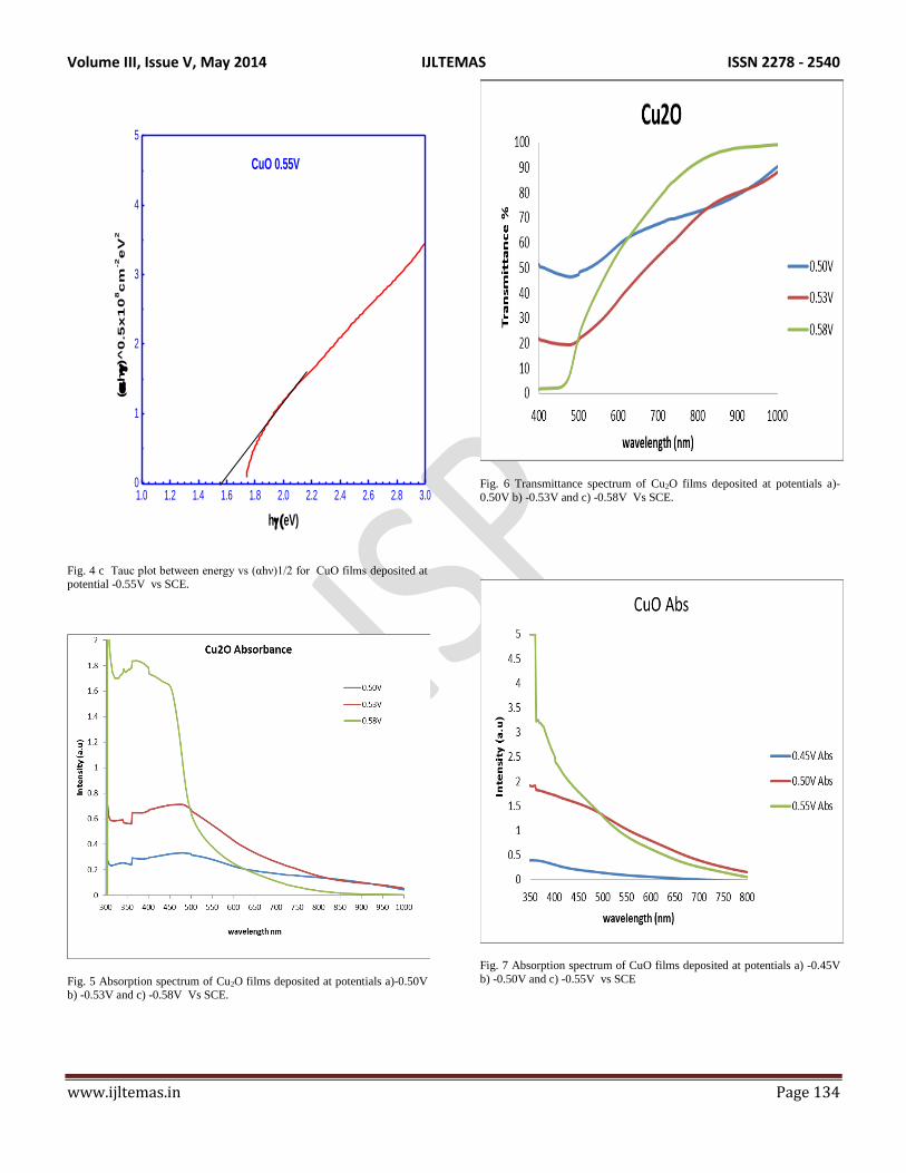
For Cu2Osamplesthe absorptionspectra(Fig. 5)and
transmittance spectra(Fig. 6)were recorded and similarly
for CuO samplesthe absorption spectra(Fig. 7) and
transmission spectra(Fig 8) were recorded. It clearly shows
that strong absorption occurs for Cu2O film deposited at
potential-0.58V and maximum absorption occurs in the blue
region for CuO thin film deposited at 0.55V.
To study the morphology SEM images were
recorded for all the prepared samples of Cu2O (Fig. 9a,Fig.
9b, Fig 9c) and CuO (Fig. 10a,Fig. 10b, Fig 10c).At
potential -0.50V cubic shaped polycrystalline grains of
Cu2O are observed and the amount of grains
Volume III, Issue V, May 2014 IJLTEMAS ISSN 2278 - 2540
www.ijltemas.in Page 134
1.0 1.2 1.4 1.6 1.8 2.0 2.2 2.4 2.6 2.8 3.00
1
2
3
4
5(
h)^
0.5
x1
08c
m-2e
V2
h(eV)
CuO 0.55V
Fig. 4 c Tauc plot between energy vs (αhν)1/2 for CuO films deposited at potential -0.55V vs SCE.
Fig. 5 Absorption spectrum of Cu2O films deposited at potentials a)-0.50V
b) -0.53V and c) -0.58V Vs SCE.
Fig. 6 Transmittance spectrum of Cu2O films deposited at potentials a)-
0.50V b) -0.53V and c) -0.58V Vs SCE.
Fig. 7 Absorption spectrum of CuO films deposited at potentials a) -0.45V
b) -0.50V and c) -0.55V vs SCE

Volume III, Issue V, May 2014 IJLTEMAS ISSN 2278 - 2540
www.ijltemas.in Page 135
Fig. 8 Transmittance spectrum of CuO films deposited at potentials a) -
0.45V b) -0.50V and c) -0.55V vs SCE.
Fig. 9a SEM Photographs of the Cu2O film deposited at potential -0.50V
Vs SCE
increases with increasing the deposition potential from -
0.53V to -0.58V Vs SCE.Similarly in CuO formation the
particles covers the entire region of the plate as the potential
Fig. 9b SEM Photographs of the Cu2O film deposited at potential -0.53V
Vs SCE
Fig. 10 a SEM Photographs of the CuO film deposited at potential 0.45V vs
SCE
increases. SEM image shows that well covered Cu2O and
CuO layers can be deposited on ITO plate .

Volume III, Issue V, May 2014 IJLTEMAS ISSN 2278 - 2540
www.ijltemas.in Page 136
Fig. 9c SEM Photographs of the Cu2O film deposited at potential -0.58V Vs SCE
Fig. 10 b SEM Photographs of the CuO film deposited at potential vs SCE-
0.50V Vs SCE.
Fig. 10 c SEM Photographs of the CuO film deposited at potential 0.55V
Vs SCE.
IV. CONCLUSION
Cu2O and CuO thin films weresuccessfully grown
on Indium Tin Oxide coated glass substrate by electro
deposition method using a single alkaline solution by giving
cathodic and anodic potentials to the substrate. The pH
value for the cathodic deposition was maintained at pH=11
and for the anodic deposition the solution pH, 13. The films
were grown for different potentials. The structural, optical
and surface morphology were analysed by XRD, UV-Vis
and SEM studies.
The XRD report shows that the cubic Cu2O and
monoclinic CuO films grown are of polycrystalline in
nature. The preferred orientation for Cu2O film is (111)
plane and for CuO (002) plane is predominant. The values
of grain sizes are calculated by Debye Scherrer formula and
are found to be in the range from 45 nm to 73nm for Cu2O
thin film and for CuO the values are from 33 nm to 39 nm.
The film thickness is controlled by optimising the time. The
optical band gap value varies from 1.75 eV to 2.35 eV for
the cuprous oxide film and from 1.3 eV to 1.55eV for the
cupric oxide thin film. This agrees well with the standard
band gap values of both Cu2O and CuO films. Also the band
gap values are found to increase when the particle size
decreases. This method paves an easy way to prepare CuO
and Cu2O from the same solution. Also, this technique may
well be considered to prepare Cu2O and CuO based solar
cells.

Volume III, Issue V, May 2014 IJLTEMAS ISSN 2278 - 2540
www.ijltemas.in Page 137
REFERENCES
[1] Balamurugan, B., and Mehta, B.R.., (2001). Optical and Structural
Properties ofNanocrystalline Copper Oxide Thin Films Prepared by Activated Reactive Evaporation.Thin Solid Films, 396, 90.
[2] Samarasekara, P. (2010). Characterization Of Low Cost P-Cu2o/N-
CuOJunction GESJ: Physics, 2(4), 3-7. [3] Takeshi Fujiwara, Takuya Nukaue, Masahino Yoshimura, (2004).
Solid State Iconics, 175,541-544.
[4] Musa, A.O., Akomolafe T., Carter M.J., (1998). Sol. Energy Mater. Sol Cells, 51, 305.
[5] Mahalingam, T., Chitra , J.S.P., Chu, J.P., Velumani , S., Sebastian,
P.J.,2005). Structural and Annealing Studies of Potentiostatically Deposited Cu2O Thin Films Solar Energy Materials & Solar Cells 88,
209 – 216.
[6] Nakaoka, K., Ueyama, J., and Ogura, K., (2004).
PhotoelectrochemicalBehaviour of Electrodeposited CuO and Cu2O
Thin Films on Conducting Substrates, Journal of the Electrochemical
Society,151(10),C661-C665. [7] Li, J., Vizkelethy, G., Revesz, P., Mayer, J. W., and Tu, K.N., (1991).
J. Appl. Phys., 9, 1020.
[8] Siripala, W., Perera, L.D.R.D., De Silva, K.T.L., Jayanetti, J.K.D.S.,
Dharmadasa, I.M., (1996). Study of Annealing Effects of Cuprous
Oxide Grown byElectrodeposition Technique Solar Energy Materials and Solar Cells, 44, 251-260.
[9] Ozawa, K.,Oba Y., Edamota, K., (2009).Formation and
Characterization ofthe Cu2O Overlayer on Zn(0001) Journal of Science, 603(13), 2163-2170.
[10]Nahle, A. and Walsh, F., (1994). Bull. Electrochem.,10, 401.
[11] Yoon, K. H.,Choi,W. J., and Kang, D. H., (2000). Photoelectrochemical Properties of Copper Oxide Thin Films Coated
on an n-Si Substrate, Thin Solid Films, 372, 250.
[12] PhilippePoizot, Chen-Jen Hung, Maxim, P., Nikiforov, Bohannan
Eric W., and Switzer, Jay A., (2003). An Electrochemical Method forCuO Thin Film Deposition from Aqueous Solution, Electrochem.
Solid-State Lett.6(2), 21-25.
[13]Madelung, O., (1996). Semiconductors, Basic Data. Springer-Verlag, Gernany,11.
[14]Sekhar, C.R., (2001). Preparation of Copper Oxide Thin Film by the
Sol-gel-like Dip Technique and Study of their Structural and Optical Properties. Solar Energy Materials & Solar Cells, 68,307.
[15] Maruyama, T., (1998). Copper Oxide Thin Films Prepared by
ChemicalVapour Deposition from Copper Dipivaloylmethonate, Elsevier, 56. [16]Shabbir, A., and Bashaar. (1998). Study of Indium Tin Oxide for
Novel optoelectronic Devices, Kings College, University of London. [17] Fan, J.C.C., and Good Enough, J.B., (1977). X-ray Photoemission
Spectroscopy Studies of S Doped ITO Film, Journal of Applied
Physics 48(8), 3524-3531. [18] Rakhshani A.E., (1986). Solid State Electronics, 29, 7.
[19] Tang, Yinwe., Zhigang Chen, ZhijieJia, Lisha Zhang, Jialin Li,
(2005).Electrodeposition and Characterization of Nanocrystalline Cuprous Oxide Thin Films on TiO2 films, Materials Letters 59, 434–
438.
[20] Wijesundera, RuwanPalitha., Masanori Hidaka, Keiko Koga,Jae- Young Choi, Nark Eon Sung, (2010). Structural And Electronic
Properties of Electrodeposited HeterojunctionOfCuO/Cu2O,
Ceramics – Silikáty54 (1) 19-25. [21] Septina, Wilman, (2014). Electrochemical Deposition of Cu2O Layer
and their Solar Cell Properties, Master Thesis, Published in
Academia.edu<.http://www.academia.edu/574519/Electrochemic al_Deposition_of_Cuprous_Oxide_Layers_and_Their_Solar_Ce
ll_Properties>


![Volume III, Issue V, May 2014 IJLTEMAS ISSN 2278 - 2540 ......hopping from Mn3+ to Mn4+,defined as t = t 0 cos( /2) [17] (where t 0 is the normal transfer integral and is the angle](https://img.dokumen.tips/doc/110x75/60d6d0c9af536462053d8339/volume-iii-issue-v-may-2014-ijltemas-issn-2278-2540-hopping-from-mn3.jpg)