Embed Size (px)
Citation preview

inside News Review, News Analysis, Features, Research Review, and much more...Free Weekly E News round up go to: www.compoundsemiconductor.net
LEDs: Building better greens with cubic GaN
Producing III-V FETs on large silicon substrates
Enhancing smartphones with superior BiHEMTs
Understanding changes within the SiC industry
Reducing failures for GaN-on-GaN diodes
GaN LEDsSpanning the visible spectrum
Volume 22 Issue 8 November / December 2016 @compoundsemi www.compoundsemiconductor.net
Front Cover CS v3RS.indd 1 28/11/2016 13:01

Untitled-5 1 29/06/2016 15:50

ViewpointBy Dr Richard Stevenson, Editor
COPYRIGHT COMPOUND SEMICONDUCTOR l NOVEMBER / DECEMBER 2016 l WWW.COMPOUNDSEMICONDUCTOR.NET 3
Compound Semiconductor is published eight times a year on a controlled circulation basis. Non-qualifying individuals can subscribe at: £105.00/e158 pa (UK & Europe), £138.00 pa (air mail), $198 pa (USA). Cover price £4.50. All information herein is believed to be correct at time of going to press. The publisher does not accept responsibility for any errors and omissions. The views expressed in this publication are not necessarily those of the publisher. Every effort has been made to obtain copyright permission for the material contained in this publication. Angel Business Communications Ltd will be happy to acknowledge any copyright oversights in a subsequent issue of the publication. Angel Business Communications Ltd © Copyright 2016. All rights reserved. Contents may not be reproduced in whole or part without the written consent of the publishers. The paper used within this magazine is produced by chain of custody certifi ed manufacturers, guaranteeing sustainable sourcing.US mailing information: Compound Semiconductor, ISSN 1096-598X, is published 8 times a year, Jan/Feb, March, April/May, June, July, August/September, October, November/ December by Angel Business Communications Ltd, Unit 6, Bow Court, Fletchworth Gate, Burnsall Rd, Coventry CV5 6SP. UK. The 2016 US annual subscription price is $198. Airfreight and mailing in the USA by agent named Air Business Ltd, c/o Worldnet Shipping Inc., 156-15, 146th Avenue, 2nd Floor, Jamaica, NY 11434, USA. Periodicals postage paid at Jamaica NY 11431. US Postmaster: Send address changes to Compound Semiconductor, Air Business Ltd, c/o Worldnet Shipping Inc., 156-15, 146th Avenue, 2nd Floor, Jamaica, NY 11434, USA. Printed by: Pensord Press. ISSN 1096-598X (Print) ISSN 2042-7328 (Online) © Copyright 2016.
Editor Richard Stevenson [email protected] +44 (0)1291 629640Contributing Editor Rebecca Pool [email protected] Editor Christine Evans-Pughe [email protected] Senior Sales Executive Robin Halder [email protected] +44 (0)2476 718979Sales & Marketing Shehzad Munshi [email protected] +44 (0)1923 690215USA Representatives Tom Brun Brun Media [email protected] +001 724 539-2404 Janice Jenkins [email protected] +001 724-929-3550 Amy Rogers [email protected] +001 678-714-6775Publisher Jackie Cannon [email protected] +44 (0)1923 690205Director of Logistics Sharon Cowley [email protected] +44 (0)1923 690200Design & Production Manager Mitch Gaynor [email protected] +44 (0)1923 690214
Circulation Director Jan Smoothy [email protected] +44 (0)1923 690200Chief Operating Offi cer Stephen Whitehurst [email protected] +44 (0)2476 718970Directors Bill Dunlop Uprichard – CEO, Stephen Whitehurst – COO, Jan Smoothy – CFO, Jackie Cannon, Scott Adams, Sharon Cowley, Sukhi Bhadal, Jason Holloway
Published by Angel Business Communications Ltd, Hannay House, 39 Clarendon Road, Watford, Herts WD17 1JA, UK. T: +44 (0)1923 690200 E: [email protected]
Accounts & Multi Media Angel Business Communications Ltd, Unit 6, Bow Court, Fletchworth Gate, Burnsall Road, Coventry CV5 6SP, UK. T: +44 (0)2476 718 970 E: [email protected]
Full colour GaNTODAY the LEDs emitting in the blue and green are made from the nitrides, while arsenides enable the construction of the orange, yellow and red emitting cousins.
Trimming the number of material systems from these two to just one would be better on multiple fronts. It would simplify packaging; it would allow driving systems to be optimised for specifi c electrical and material characteristics; and it would open the door to the production of full-colour LED displays and white-lighting systems based on a single chip.
When exploring this route, there is no question which material system should be used: it has to be the nitrides, because the arsenides can’t stretch to shorter wavelengths, due to a switch to an indirect bandgap. Ditching arsenide devices would also lead to other benefi ts, because their effi ciency plummets at higher temperatures, and their wavelength shift with current exceeds that for nitrides.
Efforts to extend nitride LEDs from the green to yellow, orange and red are already well underway. Success is not easy, however, as quantum wells must be rich in indium to reach these wavelengths – and that impairs material quality, and ultimately effi ciency. Making matters worse, internal electric fi elds increase in strength at longer wavelengths, pulling electrons and holes further apart and hampering radiative recombination.
One way to improve performance is to reduce the strain in these devices. For example, when a team from Ostendo Technologies
inserted a compliance layer beneath the active region, they produced the world’s fi rst GaN LED delivering tuneable, full-colour emission. This chip features intermediate carrier-blocking layers to control electron and hole transport between the quantum wells emitting in the red, green and blue (see p. 44).
Ostendo is now developing its technology for the display market. The promise of replacing backlit screens with those based on LED pixels is very attractive, as it could lead to simpler, more robust displays with greater effi ciency.
Researchers in Japan are also developing long-wavelength nitride LEDs. A partnership between scientists at Tokyo University of Science and Meijo University has developed a hybrid LED featuring an orange-emitting quantum well stacked on a blue one. The latter does not actually emit, instead serving as a strain releasing layer (see p. 58).
For both teams, emission effi ciency must increase at longer wavelengths. That’s not surprising, given that this technology is in its infancy. But hopefully great advances will be made, leadin g to widespread commercial adoption of full-colour GaN LEDs.
ViewPoint v6MGRS.indd 3 28/11/2016 12:49

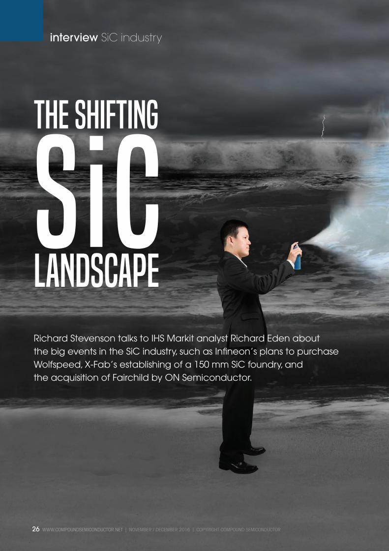
26 The shifting SiC landscape
Richard Stevenson talks to IHS Markit analyst Richard Eden about the big events in the SiC industry, such as Infineon’s plans to purchase Wolfspeed, X-Fab’s establishing of a 150 mm SiC foundry, and the acquisition of Fairchild by ON Semiconductor.
30 III-V CMOS transistors on 300 mm silicon for logic applications
InGaAs MOSFETs, and in general III-V on 300 mm silicon, remain channel materials of interest for future technology application.
38 BiHEMTs: Developing a high-volume, high-yield process
Tackling topology-related issues holds the key to high-volume, high-yield BiHEMT production.
4 WWW.COMPOUNDSEMICONDUCTOR.NET l NOVEMBER / DECEMBER 2016 l COPYRIGHT COMPOUND SEMICONDUCTOR
CONTENTS
48 Reducing initial failures in GaN-on-GaN vertical diodes
Eradicating epi-layer growth pits in GaN-on-GaN diodes boosts yield by reducing failures associated with low breakdown voltages.
54 Green LEDs: The case for cubic GaN
Green LEDs formed from cubic GaN can have lower Auger losses, higher hole carrier mobility, greater optical gain and increased p-doping efficiency.
VOLUME 22 ISSUE 8 2016
44
44 The world’s first monolithic full-colour LED
Ultra-high-resolution flexible displays will benefit from microLEDs that efficiently emit all three primary colours.
COVER STORY
Contents CS v3.indd 4 28/11/2016 13:00
COPYRIGHT COMPOUND SEMICONDUCTOR l NOVEMBER / DECEMBER 2016 l WWW.COMPOUNDSEMICONDUCTOR.NET 5
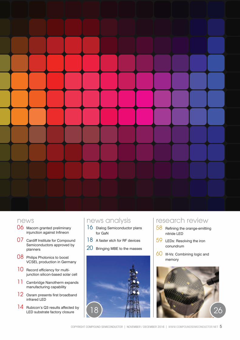
news06 Macom granted preliminary injunction against Infineon
07 Cardiff Institute for Compound Semiconductors approved by planners
08 Philips Photonics to boost VCSEL production in Germany
10 Record efficiency for multi- junction silicon-based solar cell
11 Cambridge Nanotherm expands manufacturing capability
12 Osram presents first broadband infrared LED
14 Rubicon’s Q3 results affected by LED substrate factory closure
news analysis16 Dialog Semiconductor plans for GaN
18 A faster etch for RF devices
20 Bringing MBE to the masses
research review58 Refining the orange-emitting nitride LED
59 LEDs: Resolving the iron conundrum
60 III-Vs: Combining logic and memory
18 26
Contents CS v3.indd 5 28/11/2016 13:00

6 WWW.COMPOUNDSEMICONDUCTOR.NET l NOVEMBER / DECEMBER 2016 l COPYRIGHT COMPOUND SEMICONDUCTOR
news reviewsMacom granted preliminary injunction against InfineonMACOM, a US company that makes RF, microwave and photonic semiconductors, has been granted a preliminary injunction in its lawsuit against Infineon Technologies Americas Corp over GaN-on-silicon technology rights.
The US District Court for the Central District of California in Los Angeles’ decision confirmed Macom’s continuing exclusive rights in certain GaN-on-silicon RF fields under a 2010 License Agreement entered into between Nitronex (acquired by Macom in 2014) and International Rectifier (acquired by
Infineon in 2015); and it ruled that Macom is likely to succeed on its claim that Infineon’s purported termination of that Agreement was improper and without effect.
It granted Macom’s motion for a preliminary injunction prohibiting Infineon from engaging in activities inconsistent with the 2010 License Agreement pending the Court’s final decision in the case.
“We were forced to file this lawsuit to stand up to Infineon’s bullying and anticompetitive behaviour. We are
gratified by the Court’s preliminary decision confirming that the GaN-on-silicon rights granted to us under the 2010 License Agreement remain in full force and effect and that Infineon acted improperly in trying to operate in our exclusive field of use,” said John Croteau, president and CEO of Macom.“We are firmly committed to vigorously litigating this case to its rightful conclusion. We continue on the path to providing GaN-on-silicon technology that promises to improve network data service and cell coverage of 4G/LTE and 5G base stations that will benefit people worldwide.”
Qorvo reports 22.1 percent year-over-year growthUS RF COMPANY Qorvo has announced financial results for Q2 2017, ended October 1, 2016. On a GAAP basis, Q2 2017 revenue increased 22.1 percent year-over-year and 23.8 percent sequentially to $864.7 million. Gross margin was 36.6 percent, operating income was $45.4 million, and net income was $11.8 million, or diluted EPS of $0.09.
On a non-GAAP basis, gross margin was 42.8 percent, operating expenses were $172.9 million, operating income was $196.8 million, or 22.8 percent of sales, and net income was $170.4 million, or diluted EPS of $1.29.
Gross margin decreased sequentially on both a GAAP and non-GAAP basis, due primarily to lower than expected manufacturing yields during a steep product ramp to a large customer.
Bob Bruggeworth, president and chief executive officer of Qorvo, said: “The Qorvo team did an excellent job delivering 22 percent year-over-year growth and achieving our goal of non-GAAP operating expenses at 20 percent of sales.”
“At the same time, we made progress advancing core technologies and
developing highly integrated Qorvo solutions for large customer opportunities in 2017 and 2018.”
“It’s clear we have work to do on gross margin, and we’ve taken steps to address it. We continue to drive toward our operating model, including above-market revenue growth and non-GAAP operating income above 30 percent.Separately, we are pleased to announce that Qorvo’s board of directors this week has authorized a $500 million share repurchase program.”
Qorvo currently believes the demand environment in its end markets supports the following non-GAAP expectations for the December 2016 quarter: quarterly revenue in the range of $800 million to $840 million; sequential gross margin expansion of 100 to 200 bps; tax rate of approximately 8 percent; and diluted EPS in the range of $1.15 to $1.35.
German government withdraws approval for Aixtron takeoverTHE GERMAN MINISTRY of Economics has withdrawn its clearance certificate for the takeover the German semiconductor deposition firm Aixtron by Grand Chip Investment GmbH, a 100 percent indirect subsidiary of Fujian Grand Chip Investment Fund LP.Fujian Grand Chip Investment Fund is a Chinese investment fund; 51 percent of which is held by the Chinese businessman Zhendong Liu and 49 percent by Xiamen Bohao Investment Ltd. Back in May, the companies entered into a €670 million takeover agreement under which Aixtron shareholders would be offered €6.00 in cash per each ordinary share.
Aixtron has not given a reason for the reversal of the decision, but commentators in the press have highlighted growing concerns in Germany about the acquisition of cutting-edge technologies by Chinese firms and subsequent loss of knowhow and high-tech jobs.
News CS v2.indd 6 28/11/2016 12:57

COPYRIGHT COMPOUND SEMICONDUCTOR l NOVEMBER / DECEMBER 2016 l WWW.COMPOUNDSEMICONDUCTOR.NET 7
news review s
THE LATEST PHASE of Cardiff University’s £300 million Innovation Campus, which includes The Institute for Compound Semiconductors – a unique UK-based translational research centre in compound semiconductors – and Cardiff Catalysis Institute for chemical research – has been approved by city planners. Cardiff University hopes to start work on site early in 2017.
The fully-funded £135 million project on the city’s brownfield Maindy Park is the latest phase in Cardiff’s mission to embed innovation into University life. Two new buildings will bring researchers, businesses, public sector backers and students together. Architecture practices Hawkins\Brown and HOK each designed a building for the project, working alongside site master planners BDP and town planning consultancy DPP. The campus vision, outlined two years ago by vice-chancellor Colin Riordan, establishes centres of excellence that push benefits back into the economy to create a self-sustaining cycle for growth. Riordan said: “A new campus helps us create opportunities for all. Cutting-edge research, technology transfer, business development and student enterprise will put ideas to work.
“Our innovation ambitions go beyond the sum of the physical buildings. We are hiring internationally-renowned academics who can build world-class teams of post-doctoral researchers. We are equipping students with the skills they’ll need to set up future ventures. And we’re continuing to attract major UK and international funding across private and public sectors to make Cardiff the home of innovation.”
In addition to two new buildings, each covering 12,000 sq m, this latest third phase includes a bridge linking Cardiff Business School with the Innovation Campus.
Adrian Gainer, regional leader for HOK’s Science + Technology group, added: “We look forward to creating cutting-edge facilities that will reinforce the university’s international reputation as a leading catalysis research centre and build on its strengths in the development of semiconductor devices and materials. Both the Institute for Compound Semiconductors and the Cardiff Catalysis Institute have been designed to enable multidisciplinary research to flourish, with inspiring spaces to attract and retain the most talented individuals.”
Cardiff Institute for Compound Semiconductors approved by planners
Martin Jones, BDP, said: “The Campus fulfils a number of aspirations for Cardiff University and aims to facilitate world-leading scientific research, inter-disciplinary mixing and increase student opportunities in an environment that’s better for business.”
Gareth Hooper, DPP, added: “We worked very closely with the University and Cardiff Council to ensure that this exciting scheme could be delivered within an outline planning consent dating back to 2010. The result is the continuation of an exciting regeneration project, delivering physical change to the city through world-leading science.”
Visible LED communications in the darkRESEARCHERS at Dartmouth College, New Hampshire, working on a project called ‘DarkLight’ have developed and demonstrated for the first-time, how visible light from LED lighting can be used to transmit data even when the light appears dark or off.
The study, The DarkLight Rises: Visible Light Communication in the Dark was presented in New York at MobiCom 2016: The 22nd Annual International Conference on Mobile Computing and Networking on October 4th by Dartmouth co-author Zhao Tian, the lead PhD student for the project.
Through DarkLight, light-based communication is sustained even when
LEDs emit extremely low luminance, by encoding data into ultra-short, imperceptible light pulses by using off-the-shelf, low-cost LEDs ($7 each) and photodiodes ($6-8 each). The current DarkLight prototype supports 1.6 kbps data rate at 1.8 m distance.
“With DarkLight, we can potentially enable light sensing so that it is always on, 24/7, regardless of the light’s illumination status,” says the project’s principal investigator Xia Zhou, assistant professor of computer science and co-director of the DartNets (Dartmouth Networking and Ubiquitous Systems Lab), which helped conduct the study. DartNets’ research focuses on broad applications, systems, and networking
perspectives of smartphones and smart device systems.
“DarkLight shows new possibilities on what visible light alone can do. We believe there are a lot more interesting applications yet to come,” added Zhou.
News CS v2.indd 7 28/11/2016 12:57

8 WWW.COMPOUNDSEMICONDUCTOR.NET l NOVEMBER / DECEMBER 2016 l COPYRIGHT COMPOUND SEMICONDUCTOR
news reviews
Advanced Compound Semiconductor Foundry Services
Advanced III-V semiconductor solutions for optoelectronics
application in the biotechnology, telecommunications,
energy, industrial, and defense industries.
MasimoSemiconductor.com | 603-595-8900 semiconductor
M O C V D • Fa b r i c at i o n • Te s t i n g
P H O T O D E T E C T O R S
L E D S
S O L A R C E L L S
V C S E L S
T H E R M O P H O T O V O LT A I C C E L L S
L A S E R P O W E R C O N V E R T E R S
FT_337A, Ad, Compound Semiconductor Publication, Masimo Semiconductor, 189x79mm, v3.indd 1 5/10/16 4:42 PM
Philips Photonics to boost VCSEL production in GermanyPHILIPS PHOTONICS, a wholly owned business of Royal Philips, has announced that it is doubling capacity at its laser-diode facility in Ulm to provide the key components for some of the latest developments in data communication, consumer sensing and industrial thermal processing.
VCSEL diodes are key components in a growing number of consumer and industrial applications, including: sensing of 3D objects in autonomous vehicles; PC ‘mice’; industrial sensors and control functions; driver assist systems; ultra-fast data transmission in data centres
and servers; and providing distance and gesture recognition in mobile phones.
“Over the past few years, we have invested steadily in research, product development and effi cient manufacturing processes. Today, our products are widely used in datacentres, smartphones and a number of industrial applications. The sharp rise in demand for VCSELs is a key factor in our capacity expansion at Ulm, and will enable us to respond to the needs of these rapidly growing markets,” said Joseph Pankert, general manager, Philips Photonics. Semiconductor lasers have been developed and manufactured
at the Philips Photonics facility in Ulm since 2000. The company has pioneered many innovations such as VCSEL arrays, now widely used for time-of-fl ight and 3d depth imaging. Since its establishment, the facility has grown signifi cantly, with staff numbers increasing from 50 in 2012 to 200 in 2016.
In 2014, the company made signifi cant step to highly automated manufacturing, within the framework of the ‘VIDAP’ project, jointly sponsored by the German Federal Ministry of Education and Research (BMBF) and the EU.
GaN power to reach $280 million in 2021IN its Power GaN 2016: Epitaxy and Devices, Applications, and Technology Trends report, Market research fi rm Yole Développement predicts that the GaN power business will reach $280 million in 2021, growing at 86 percent CAGR between 2015 and 2021.
It says the market is being driven by emerging applications including power supplies for datacentre and telecom, AC fast chargers, Lidar, envelope tracking, and wireless power.
“Numerous powerful developments and key collaborations have been announced during this period and confi rmed a promising and fast-growing industry”, comments Hong Lin from Yole. Collaborations include Integrated Device Technology (IDT) and Effi cient Power Conversion (EPC); Infi neon Technologies
and Panasonic; Exagan and XFab; TSMC and GaN Systems for volume production, which all took place within the last two years.
Up until late 2014, 600V/650V GaN HEMTs’ commercial availability was still questionable, despite announcements from various players. Fast-forward to 2016 and end users can buy low-voltage GaN (<200V) devices from EPC and high-voltage (600V/650V) components from several players, including Transphorm, GaN Systems, and Panasonic.
The idea of bringing GaN from the power semiconductor market to the much bigger analogue IC market is also now gaining interest, says Yole. For example, EPC Power and GaN Systems are both working on more integrated solutions.
News CS v2.indd 8 28/11/2016 12:57

FIVE KEY THEMES:£ Revolutionising RF chips Will GaN RF deliver the best bang per buck by increases transistor voltages, or making these devices on silicon? And what are the best options for really high frequencies?£ Exploiting heterogeneous integration What are the fruits of a marriage between silicon and the III-Vs? And can higher mobility materials improve microprocessors and memory?£ Optimising light emitters Are colossal LED fabs revolutionising chip manufacture? And what are the big opportunities for visible lasers?£ Perfecting power electronics Can the best devices stem from the ultra-wide bandgap of gallium oxide? Or will they emerge from foundries processing GaN and SiC on silicon?£ Refining handset architectures for the 2020’s Will handsets be crammed with ever more III-V content? And could GaN appear in the front-end in the coming years?
Book your place now. Limited spaces available
Connecting, informing and inspiring the compound semiconductor industry
Speakers represent the biggest chipmakers and the most promising start-ups. PRESENTATIONS INCLUDE: £ San’an: The creation of the biggest LED chipmaker in China£ Flosfia: Unleashing the potential of gallium oxide£ Skyworks: Front-end architectures for tomorrow’s smartphones£ IBM: The latest efforts to develop III-V logic
7 - 8 March 2017Sheraton Brussels Airport Hotel, Belgium
CS International will provide comprehensive coverage of all aspects of the compound semiconductor industry
Register: www.cs-international.net
New CS International 2017 Early Bird Ad 210 x 297 v5.indd 1 25/11/2016 15:52

10 WWW.COMPOUNDSEMICONDUCTOR.NET l NOVEMBER / DECEMBER 2016 l COPYRIGHT COMPOUND SEMICONDUCTOR
news reviewsRecord efficiency for multi-junction silicon-based solar cellRESEARCHERS at the Fraunhofer Institute for Solar Energy Systems ISE together with the Austrian company EV Group (EVG) have successfully manufactured a silicon-based multi-junction solar cell with two contacts and an efficiency of 30.2 percent, exceeding the theoretical limit of silicon solar cells.
For this achievement, the researchers used a ‘direct wafer bonding’ process to transfer a few micrometres of III-V semiconductor material to silicon, a well-known process in the microelectronics industry. After plasma activation, the subcell surfaces are bonded together in vacuum by applying pressure. The atoms on the surface of the III-V subcell form bonds with the silicon atoms, creating a monolithic device.
The efficiency achieved by the researchers presents a first-time result for this type of fully integrated silicon-based multi-junction solar cell. The complexity of its inner structure is not evident from its outer appearance: the cell has a simple front and rear contact just as a conventional silicon solar cell and therefore can be integrated into photovoltaic modules in the same manner.
“We are working on methods to surpass the theoretical limits of silicon solar cells,” says Frank Dimroth, department head at Fraunhofer ISE. ‘”It is our long-standing experience with silicon and III-V technologies that has enabled us to reach this milestone today.” A conversion efficiency of 30.2 percent for the III-V / silicon multi-junction solar cell of 4 cm2 was measured at Fraunhofer ISE’s calibration laboratory. In comparison, the highest efficiency measured to date for a pure silicon solar cell is 26.3 percent, and the theoretical efficiency limit is 29.4 percent.
The III-V / silicon multi-junction solar cell consists of a sequence of subcells stacked on top of each other. So-called ‘tunnel diodes’ internally connect the three subcells made of GaInP, GaAs and silicon, which span the absorption range of the sun’s spectrum.
The GaInP top cell absorbs radiation between 300 and 670 nm. The middle GaAs subcell absorbs radiation between 500 and 890 nm and the bottom silicon subcell between 650 and 1180 nm, respectively.
The III-V layers are first epitaxially deposited on a GaAs substrate and then bonded to a silicon solar cell structure. Subsequently the GaAs substrate is removed, and a front and rear contact as well as an antireflection coating are applied. “Key to the success was to find a manufacturing process for silicon solar cells that produces a smooth and highly doped surface which is suitable for wafer bonding as well as accounts for the different needs of silicon and the applied III-V semiconductors,” explains Jan Benick, team leader at Fraunhofer ISE. “In developing the process, we relied on our decades of research experience in the development of highest efficiency silicon solar cells.”
Institute director Eicke Weber said: “I am pleased that Fraunhofer ISE has so convincingly succeeded in breaking through the glass ceiling of 30 percent efficiency with its fully integrated silicon-based solar cell with two contacts. With this achievement, we have opened the door for further efficiency improvements for cells based on the long-proven silicon material.”
“The III-V / silicon multi-junction solar cell is an impressive demonstration of the possibilities of our ComBond cluster for resistance-free bonding of different
semiconductors without the use of adhesives,’ says Markus Wimplinger, corporate technology development and IP director at EV Group.
“Since 2012, we have been working closely with Fraunhofer ISE on this development and today are proud of our team’s excellent achievements.” The direct wafer-bonding process is already used in the microelectronics industry to manufacture computer chips.
On the way to the industrial manufacturing of III-V / silicon multi-junction solar cells, the costs of the III-V epitaxy and the connecting technology with silicon must be reduced. There are still great challenges to overcome in this area, which the Fraunhofer ISE researchers intend to solve through future investigations. Fraunhofer ISE’s new Centre for High Efficiency Solar Cells, presently being constructed in Freiburg, will provide them with the perfect setting for developing next-generation III-V and silicon solar cell technologies. The ultimate objective is to make high efficiency solar PV modules with efficiencies of over 30 percent possible in the future.
The young researcher Romain Cariou carried out research on this project at Fraunhofer ISE with the support of a Marie Curie Postdoctoral Fellowship. Funding was provided by the EU project HISTORIC. The work at EVG was supported by the Austrian Ministry for Technology.
News CS v2.indd 10 28/11/2016 12:58
COPYRIGHT COMPOUND SEMICONDUCTOR l NOVEMBER / DECEMBER 2016 l WWW.COMPOUNDSEMICONDUCTOR.NET 11
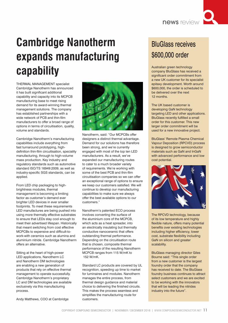
news review sBluGlass receives $600,000 orderAustralian green technology company BluGlass has received a significant order commitment from a new UK customer for its specialist epitaxy development. Worth around $600,000, the order is scheduled to be delivered over the next 12 months.
The UK based customer is developing GaN technology targeting LED and other applications. BluGlass recently fulfilled a small order for this customer. This new larger order commitment will be used for a new innovative project.
BluGlass’ Remote Plasma Chemical Vapour Deposition (RPCVD) process is designed to grow semiconductor materials such as GaN and InGaN with advanced performance and low cost potential.
The RPCVD technology, because of its low temperature and highly flexible nature, offers many potential benefits over existing technologies including higher efficiency, lower cost, substrate flexibility including GaN on silicon and greater scalability.
BluGlass managing director Giles Bourne said: “This single order from a new customer is the largest foundry order that the company has received to date. The BluGlass foundry business continues to attract select customers and we are excited to be working with the innovators that will be leading the nitrides industry into the future”.
Cambridge Nanotherm expands manufacturing capabilityTHERMAL MANAGEMENT specialist Cambridge Nanotherm has announced it has built significant additional capability and capacity into its MCPCB manufacturing base to meet rising demand for its award-winning thermal management solutions. The company has established partnerships with a wide network of PCB and thin-film manufacturers to offer a broad range of options in terms of circuitisation, quality, volume and standards.
Cambridge Nanotherm’s manufacturing capabilities include everything from fast turnaround prototyping, high-definition thin-film circuitisation, speciality manufacturing, through to high-volume mass production. Key industry and regulatory standards such as automotive standard ISO/TS 16949:2009, as well as industry-specific SGS standards, can be applied.
From LED chip packaging to high-brightness modules, thermal management is becoming a limiting factor as customer’s demand ever brighter LED devices in ever smaller footprints. To meet these requirements LED manufactures are being pushed into using more thermally effective substrates to ensure that LEDs stay cool enough to meet their advertised lifespan. Historically that meant switching from cost effective MCPCBs to expensive and difficult-to-work-with ceramics such as alumina and aluminium nitride. Cambridge Nanotherm offers an alternative.
Sitting at the heart of high-power LED applications, Nanotherm LC and Nanotherm DM technologies are enabling a new generation of products that rely on effective thermal management to operate successfully. Cambridge Nanotherm’s proprietary LC and DM technologies are available exclusively via this manufacturing process.
Andy Matthews, COO at Cambridge
Nanotherm, said: “Our MCPCBs offer designers a distinct thermal advantage. Demand for our solutions has therefore been strong, and we’re currently engaged with most of the top ten LED manufacturers. As a result, we’ve expanded our manufacturing routes to cater to a much broader variety of requirements. We’re working with some of the best PCB and thin-film circuitisation companies so we can offer an exceptional range of options to ensure we keep our customers satisfied. We will continue to develop our manufacturing capabilities to make sure we always offer the best available options to our customers.”
Nanotherm’s patented ECO process involves converting the surface of the aluminium core of the MCPCB, which acts as a heat spreader, into an electrically insulating but thermally conductive nanoceramic that offers outstanding thermal performance. Depending on the circuitisation route that is chosen, composite thermal performance of the resulting Nanotherm MCPCB ranges from 115 W/mK to 152 W/mK.
Standard LC products are covered by UL recognition, speeding up time to market for luminaires and modules. Nanotherm manages the entire process, from thermal design guidance and material choice to delivering the finished circuits. This makes the process seamless and simplifies the manufacturing route for customers.
News CS v2.indd 11 28/11/2016 12:58

12 WWW.COMPOUNDSEMICONDUCTOR.NET l NOVEMBER / DECEMBER 2016 l COPYRIGHT COMPOUND SEMICONDUCTOR
news reviews
313, Cheomdangwagi-ro, Buk-gu, Gwangju, South Korea 61008T +82 (62) 973-0490 F +82 (62) 973-0489 W www.hisolarled.co.kr E [email protected] or [email protected]
Reclaim ServiceSapphireSiC InP
Special Spec. Wafer for R&D Sapphire SiSiC GaN Quartz Glass
What we do?
Osram presents first broadband infrared LEDOSRAM OPTO SEMICONDUCTORS is using converter technology for infrared emitters for the first time. The result is the SFH 4735 – an LED that emits broadband infrared light in a wavelength range from 650 to 1050nm. The main application is near-infrared spectroscopy, for example for analysing food.
Infrared spectroscopy uses the characteristic absorption behaviour of certain molecular compounds. If a defined spectrum is directed at a sample it is possible to determine the presence and quantity of certain ingredients from the wavelength distribution of the reflected light. This method is used in the food industry and in agriculture, among other sectors. It is possible, for example, to measure the water, fat, carbohydrate, sugar or protein content of foodstuffs. This data provides an indication of freshness, quality or calorie content.
Osram believes that this new infrared LED opens this measurement technique
up to consumers. One option would be a compact sensor – like a USB stick – which would be used with an appropriate smartphone app to measure calories, freshness or nutritional content.
The basis of the SFH 4735 is a blue 1 mm2 chip in UX:3 technology. Its light is converted into infrared radiation with the aid of a phosphor converter developed specifically for this application.
A residual blue component in the light helps users target the area they want to investigate. The emission spectrum of the SFH 4735 has a homogeneous spectral distribution in the infrared range.
The chip is mounted in the Oslon Black Flat package which is characterised in particular by good thermal resistance.
Compact units for spectroscopic chemical analyses open up a completely new range of applications in consumer electronics. Experts expect that it will be
possible in the near future to integrate spectrometers directly in mobile devices. The new technology is a natural extension of bio monitoring, in other words the trend for measuring various vital signs such as pulse rate and calorie consumption.
A smartphone spectrometer will enable users to monitor the food they eat in a similar manner. Medicines can also be checked in the same way.
“Future applications are also of particular interest”, said Udo Jansen, product marketing manager for infrared at Osram Opto Semiconductors. “It is conceivable that the emission range can be extended to include wavelengths up to 2,000 nanometres, in other words into the middle infrared spectral range. This will allow more precise and detailed measurements and will open up new options for everyday analyses of certain environmental parameters such as air quality.”
Cree files lawsuit against Emson TacLightLED company Cree has filed a complaint against E. Mishan & Sons, Inc. (Emson) with the US District Court for the District of Massachusetts for infringement of Cree’s patented LED technology in Emson’s flashlights, such as the Bell + Howell Taclight. “Cree will not tolerate and will aggressively defend against such blatant disregard of its intellectual property rights,” said Dave Emerson, senior vice president and general manager for Cree LEDs.
“We have an obligation to our customers to ensure that the market offers products that include the high-quality LED components that customers have come to expect. We are committed to protecting Cree’s investment in research and development on behalf of our customers, shareholders and our licensing partners.”
As part of the complaint, Cree is seeking an award of enhanced damages, attorneys’ fees and an injunction to prevent Emson from offering for sale and selling any products using knock-off LEDs.
News CS v2.indd 12 28/11/2016 12:58

FIVE KEY THEMES:£ Revolutionising RF chips Will GaN RF deliver the best bang per buck by increases transistor voltages, or making these devices on silicon? And what are the best options for really high frequencies?£ Exploiting heterogeneous integration What are the fruits of a marriage between silicon and the III-Vs? And can higher mobility materials improve microprocessors and memory?£ Optimising light emitters Are colossal LED fabs revolutionising chip manufacture? And what are the big opportunities for visible lasers?£ Perfecting power electronics Can the best devices stem from the ultra-wide bandgap of gallium oxide? Or will they emerge from foundries processing GaN and SiC on silicon?£ Refining handset architectures for the 2020’s Will handsets be crammed with ever more III-V content? And could GaN appear in the front-end in the coming years?
Book your place now. Limited spaces available
Connecting, informing and inspiring the compound semiconductor industry
Speakers represent the biggest chipmakers and the most promising start-ups. PRESENTATIONS INCLUDE: £ San’an: The creation of the biggest LED chipmaker in China£ Flosfia: Unleashing the potential of gallium oxide£ Skyworks: Front-end architectures for tomorrow’s smartphones£ IBM: The latest efforts to develop III-V logic
7 - 8 March 2017Sheraton Brussels Airport Hotel, Belgium
CS International will provide comprehensive coverage of all aspects of the compound semiconductor industry
Register: www.cs-international.net
New CS International 2017 Early Bird Ad 210 x 297 v5.indd 1 25/11/2016 15:52

14 WWW.COMPOUNDSEMICONDUCTOR.NET l NOVEMBER / DECEMBER 2016 l COPYRIGHT COMPOUND SEMICONDUCTOR
news reviewsRubicon’s Q3 results affected by LED substrate factory closureRUBICON TECHNOLOGY has reported financial results for its Q3 ended September 30, 2016.
The company reported Q3 revenue of $7.1 million, $3.6 million higher than the prior quarter revenue. Revenue from wafer sales in the Q3 was $5.5 million as compared with $1.8 million in the prior quarter. The higher wafer revenue was the result of increased orders from a key patterned wafer customer along with that
customer drawing down all wafers in consignment inventory.
The company’s Q3 results were impacted by the decision made in September this year to cease all production activities and shut down its Penang, Malaysia facility. The facility has been primarily engaged in producing polished and patterned substrates for the LED market and the decision was made in order for the company to focus on the optical and
industrial sapphire market for the foreseeable future.
Production activities at the Penang facility are expected to cease by November 30, 2016, with the shutdown of the facility to be completed by the end of the year. Bill Weissman, the company’s CEO, said: “While margin pressure in the
LED and mobile device segments of the sapphire market continue to be severe, there remains good margin opportunity in the optical and industrial segments. We believe that the actions we are taking will improve our operating results, strengthen our cash position and allow us to grow in strategic markets that are better aligned with our strengths while offering stronger margin potential. Once the changes are fully implemented, our revenue will be smaller for a period of time, but the optical and industrial sapphire markets are growing with potential new applications for sapphire emerging.
“Once our Malaysia facility ceases production activities, our wafer revenue will significantly decrease beginning in the fourth quarter of 2016 and into future periods.”
One-time charges in the quarter related to the decision to exit the LED market and close the Malaysia facility included; a $10.2 million asset impairment for writing the Malaysia assets down to liquidation value, a write-down of $4.0 million in excess raw material inventory, and $900 thousand in accrued severance.
LayTec delivers 2000th in-situ metrology tool
LAYTEC has delivered its 2000th in-situ metrology system since its foundation in 1999. An EpiTT with 2000 in its serial number has been shipped to Compound Semiconductor Centre (CSC) – a joint venture between compound semiconductor specialists IQE and Cardiff University.
CSC works on providing a complete capability value chain from high-end R&D through product and process innovation to high value, large-scale manufacturing. According to Wyn Meredith, director of CSC: “This EpiTT and other LayTec systems already installed in our labs provide unrivalled precision and sophisticated analysis algorithms, which is crucial for process optimisation in semiconductor manufacturing environment.”
EpiTT - LayTec’s workhorse for MOCVD mass production – combines measurements of temperature and reflectance at three wavelengths in one tool. For True Temperature (TT), it uses Emissivity Corrected Pyrometry, which delivers the precise surface temperatures of opaque materials at 950 nm (silicon, GaAs, InP). For materials that are transparent at
950 nm (GaN, Sapphire, SiC), EpiTT measures the temperature on the top side of the carrier. Measuring reflectance at three wavelengths monitors all essential properties of the growing layers, such as growth rate, film thickness, stoichiometry changes and morphology.
LayTec’s founder and CEO Thomas Zettler commented: “It is significant that our 2000th in-situ tool is delivered to a research institution with a strong connection to industry. LayTec has always set a great value on cooperating with both industry and R&D.”
He added: “Until now, we have equipped hundreds of customers worldwide with state-of-the-art metrology, mainly in the field of LED and laser production. In the last few years we also entered the PV, display and advanced silicon markets. Meanwhile, our product portfolio covers all areas of process monitoring: in-situ, in-line, lab-line and map-line metrology. Due to this market diversification, we believe to deliver the next thousand tools much faster than before.”
News CS v2.indd 14 28/11/2016 13:01

Untitled-2 1 28/11/2016 15:06

16 WWW.COMPOUNDSEMICONDUCTOR.NET l NOVEMBER / DECEMBER 2016 l COPYRIGHT COMPOUND SEMICONDUCTOR
news analysis
LATE THIS SUMMER, UK-based Dialog Semiconductor revealed plans to sample GaN power ICs in a fast charging power adapter by the end of this financial year.
Following two years of collaboration with Taiwan Semiconductor Manufacturing Corporation, the power management IC supplier has developed a 650 V GaN power IC plus controller combination that is said to halve the size and power losses of silicon power management ICs.
“Until recently, GaN had been largely limited to small specialty fabs from vendors in Japan as well as research institutions,” says Mark Tyndall, Senior Vice President of Corporate Development and Strategy at Dialog. “In contrast, Dialog targets high volume consumer applications, so it’s never been our intention to prove GaN for, say, niche military applications.”
“But when TSMC started to offer GaN as a standard process on six inch wafers, we saw that as a signal that this was the right time to enter this market, as well as solve the emerging problems of size in the power adapter market,” he adds.
Dialog’s end-result is the so-called SmartGaN DA8801; a monolithic IC that integrates enhanced-mode GaN-on-silicon HEMTs with analogue drivers and logic blocks in a 650 V half-bridge design for 25 W to 65 W adapters. By combining this IC with its ‘Rapid Charge’ power conversion controllers, Dialog can produce efficient, small, high-power-density adapters that look set to topple traditional silicon FET-based designs from pole position in the world of power adapters.
“We’re not trying to replace a silicon FET with a pure GaN transistor; how could a six inch [GaN-on-silicon] wafer process compete with [CMOS] manufacturer
Dialog Semiconductor
PLANS FOR GaNDialog’s delivery of GaN power ICs signals mainstream market adoption is close, reports Rebecca Pool.
producing millions and millions of wafers?” points out Tyndall. “But we have optimised our solution around this GaN, half-bridge architecture which allows us to provide a GaN-based system at the same cost, or even lower, that the traditional silicon FET system.”
“We’ve reduced the overall bill of materials in our systems and we’re getting a lot of excitement as we now have a small 45 W adapter in a 25 W adapter housing,” he adds.
Crucially, this reduction in size paves the way to the universal power adapter that the mobile communications industry craves for its smartphones, notebooks, iPads and more. And according to Tyndall, Dialog customers are more than ready for GaN.
While he reckons initial concerns centred on device reliability, times have changed and industry has moved on. “We’re really are beyond these issues now,” he asserts.
Indeed, as Richard Eden, senior analyst at IHS Markit, highlights, Dialog is one of many moving towards GaN. “It’s a safe bet that all silicon semiconductor suppliers are developing a strategy for GaN,” he points out.
“During the last five years, start-ups such as Efficient Power Conversion, Transphorm and GaN Systems have successfully developed GaN products for the commercial market,” he adds. “And more recently, larger silicon semiconductor companies, such as Infineon Technologies, Texas Instruments and Panasonic, have announced GaN developments.”
For example, in March last year, Texas Instruments launched a 80 V GaN FET power-stage comprising a high-frequency driver and two GaN FETs in a half-bridge configuration.
For Eden, these developments and Dialog’s latest announcement are clear signals that GaN is now joining mainstream markets and is no longer considered to be a ‘clever research lab experiment’. “And with foundry companies like TSMC now offering a GaN-on-silicon transistor process technology
News Analysis v6MGRS.indd 16 28/11/2016 12:58

COPYRIGHT COMPOUND SEMICONDUCTOR l NOVEMBER / DECEMBER 2016 l WWW.COMPOUNDSEMICONDUCTOR.NET 17
news analysis
to clients, perhaps we will see more suppliers offering similar products using their own driver IC [technology],” he says.
State-of-playRight now, Dialog is testing its GaN-based power IC with ‘beta’ customers and is set to sample during Q4, this financial year. The company’s next move will be to ramp up production to volume levels, which Tyndall believes will take place by the middle of next year.
“We’re strong in the fast-charging, mobile, power adapter market with around a 70 percent share and we’re also entrenched with the top ten vendors in the China smartphone market,” he says.
The Development and Strategy President doesn’t foresee any supply chain issues – manufacturing uses standard CMOS equipment – but highlights: “We do need to be careful with back-end packaging and have chosen experienced vendors here.”
“We also intend to use high volume, standard, device testers, which fits with our desire to manufacture hundreds of millions of units without using niche [processes],” he adds.
Then, with wireless device markets addressed, the company intends to turn to PC markets with a 100 W power adapter, and eventually target server markets.
Looking beyond high-volume consumer markets, Dialog isn’t chasing industrial applications such as PV inverters, turbines and electric vehicles, although according to Tyndall, the company would ‘never say never’.
However, the company has settled on GaN-on-silicon as its future technology of choice, over SiC, which
Tyndall puts down to lower costs, better monolithic integration and higher volume production.“We are looking to drive production volumes now,” he concludes. “There is a chicken and egg element here as we need to drive volumes to drive the next level of fab investment that will bring us to a higher wafer size. But I would hope to move to eight inch wafers in the next two to three years.”
News Analysis v6MGRS.indd 17 28/11/2016 12:58
18 WWW.COMPOUNDSEMICONDUCTOR.NET l NOVEMBER / DECEMBER 2016 l COPYRIGHT COMPOUND SEMICONDUCTOR
news analysis
JUST LAST MONTH, Oxford Instruments revealed its latest SiC via etch process to be added to the PlasmaPro100 Polaris etch system.
Already designed to deliver fast etch rates on GaN, sapphire, SiC wafers and more, the single-wafer etch system now promises a faster, smooth via etch through SiC at a time when the wide bandgap material is proving crucial to the development of GaN-on-SiC RF devices.
“The system was released a couple of years ago, but this SiC via process is new,” says Mark Dineen, Optoelectronics Product Manager at Oxford Instruments Plasma Technology.
“We saw a market need for this, developed it and believe now is the time to release it,” he adds. “GaN-on-SiC is definitely a growing market and we want to be part of that.”
But the road to the smooth SiC via hasn’t been straightforward. SiC backside via etching is crucial to form a contact with electrodes during the fabrication of GaN-on-SiC transistors. However, SiC is a tough material to etch and researchers worldwide have grappled with how best to handle a substrate with a hardness close to that of diamond. Oxford Instruments now believes it has the answer.
New stepsAs part of the latest etch process, SiC is mounted onto a sapphire carrier using wax, ready to plasma-etch the via some 100 μm through the wafer. As Dineen highlights, this wafer thickness demands a fast, aggressive etch, and as such, process engineers at Oxford Instruments have opted for a 1.2 μm per minute etch rate. “We need smooth sidewalls in the via, and if we went faster, we would produce jagged
A faster etch for RF devicesAs GaN-on-SiC RF devices reach market, Oxford Instruments has delivered a new via etch process to ease fabrication, reports Rebecca Pool.
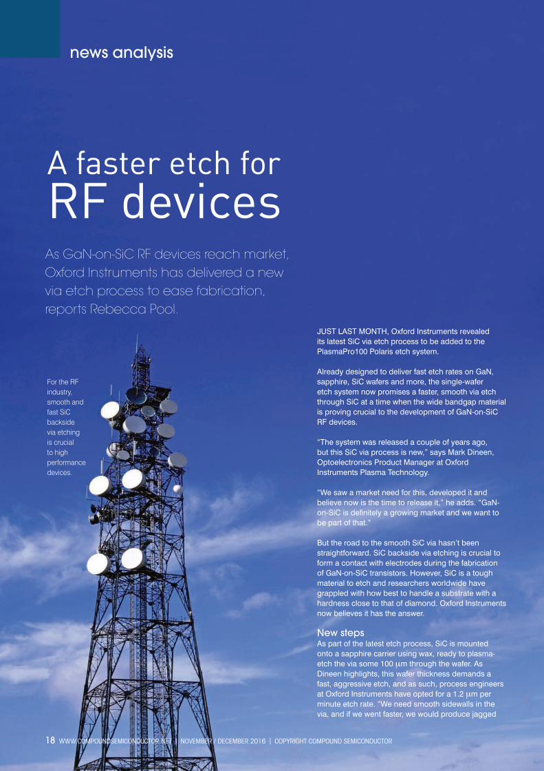
For the RF industry, smooth and fast SiC backside via etching is crucial to high performance devices.
News Analysis v6MGRS.indd 18 28/11/2016 12:58

COPYRIGHT COMPOUND SEMICONDUCTOR l NOVEMBER / DECEMBER 2016 l WWW.COMPOUNDSEMICONDUCTOR.NET 19
news analysis
features within the via which leads to localised heating and reduces device lifetime,” he says. “But any slower, then throughput is just too slow and the [system] cost of ownership is too high.”
A key issue that many researchers have encountered while optimising SiC substrate via etch processes is the formation of so-called pillars in the via hole, which impede metallisation. These unusual structures form on the end of micro-pipes – hollow tubes that are created during SiC growth – and are exposed after the relatively thick SiC wafer is chemically thinned to around 100 μm for the via etch.
Myriad researchers have experimented with pre-etch clean and etch processes to avoid pillar formation. But according to Dineen, Oxford Instruments has countered this problem by introducing a 30 second etch to the process. It smoothly removes the top layer and accompanying defects to produce a clean surface prior to the main SiC via etch.
So, with defects removed, the relatively fast, aggressive plasma-etch swiftly produces a smooth, slightly sloped via, ready for post-etch metallisation. However, this process also generates heat around the wafer and sapphire carrier, spelling bad news for the all-important wax attachments that have an upper temperature limit of 150°C.
To maintain wax integrity, the wafer is electrostatically clamped to a lower electrode, which contains liquid cooling channels to transfer heat away through the electrode. As Dineen highlights, electrostatic clamping is widely used in the silicon industry, but during this SiC via etch process, a non-conducting sapphire substrate is being handled that will adhere to the clamp at the end of the etch.
Given this, the company transferred a technology to the system that was developed as part of its past GaN-on-sapphire LED research.
“We had developed an electrostatic clamp that could efficiently clamp bare sapphire as part of our patterned sapphire substrate process,” explains Dineen. “Thanks to the control method we developed, here we have excellent cooling in our system and the wafers are handled very smoothly.”
While the company capitalises on lessons learned from LED process development, does it also expect the up and coming GaN-on-SiC RF device market to provide the same potential for growth? Dineen points
to the likes of Wolfspeed, Panasonic and Fujitsu, all developing GaN-on-SiC RF devices, and also highlights how China-based manufacturers are now penetrating the market.
Yet, an LED-type boom isn’t expected. As Dineen puts it: “We do see a lot of growth in this market, but I don’t think we will see anything quite as big as the LED market.”
“This is an interesting market, it’s growing and SiC also has potential in power applications,” he adds. “This all ties in with our expertise around III-V materials in these niche production markets.”
And what about rival GaN-on-silicon devices? For example, this time last year, MACOM celebrated shipping more than one million GaN-on-silicon RF devices while claiming a 100 W transistor with comparable performance at a cheaper cost. And more recently, imec has launched a GaN-on-silicon research programme to produce 8 inch wafers.
“Processing costs will be a barrier for GaN-on-SiC devices but its performance is driving demand,” he says. “If you measure GaN-on-SiC device quality versus cost, it is a strong choice compared to GaN-on-silicon. GaN-on-silicon will have a place for sure, although there are limitations on performance.”
Still, Oxford Instrument’s PlasmaPro100 Polaris etch system can handle wafer sizes up to 8 inches. And as Dineen concludes: “I’m not sure whether or not SiC wafers will reach that diameter, but GaN-on-silicon wafers are getting there, so we can etch a GaN recess into these wafers if needed.”
Oxford Instrument’s latest via etch process promises a via with smooth, slightly sloping sidewalls for high performance devices.
News Analysis v6MGRS.indd 19 28/11/2016 12:58
20 WWW.COMPOUNDSEMICONDUCTOR.NET l NOVEMBER / DECEMBER 2016 l COPYRIGHT COMPOUND SEMICONDUCTOR
news analysis
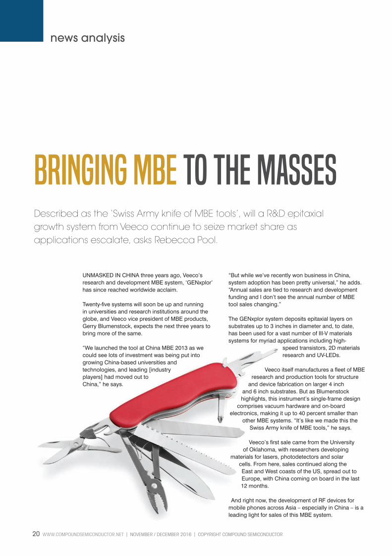
Bringing MBE to the massesDescribed as the ‘Swiss Army knife of MBE tools’, will a R&D epitaxial growth system from Veeco continue to seize market share as applications escalate, asks Rebecca Pool.
UNMASKED IN CHINA three years ago, Veeco’s research and development MBE system, ‘GENxplor’ has since reached worldwide acclaim.
Twenty-five systems will soon be up and running in universities and research institutions around the globe, and Veeco vice president of MBE products, Gerry Blumenstock, expects the next three years to bring more of the same.
“We launched the tool at China MBE 2013 as we could see lots of investment was being put into growing China-based universities and technologies, and leading [industry players] had moved out to China,” he says.
“But while we’ve recently won business in China, system adoption has been pretty universal,” he adds. “Annual sales are tied to research and development funding and I don’t see the annual number of MBE tool sales changing.”
The GENxplor system deposits epitaxial layers on substrates up to 3 inches in diameter and, to date, has been used for a vast number of III-V materials systems for myriad applications including high-
speed transistors, 2D materials research and UV-LEDs.
Veeco itself manufactures a fleet of MBE research and production tools for structure
and device fabrication on larger 4 inch and 6 inch substrates. But as Blumenstock highlights, this instrument’s single-frame design
comprises vacuum hardware and on-board electronics, making it up to 40 percent smaller than
other MBE systems. “It’s like we made this the Swiss Army knife of MBE tools,” he says.
Veeco’s first sale came from the University of Oklahoma, with researchers developing
materials for lasers, photodetectors and solar cells. From here, sales continued along the East and West coasts of the US, spread out to Europe, with China coming on board in the last 12 months.
And right now, the development of RF devices for mobile phones across Asia – especially in China – is a leading light for sales of this MBE system.
News Analysis v6MGRS.indd 20 28/11/2016 12:58
COPYRIGHT COMPOUND SEMICONDUCTOR l NOVEMBER / DECEMBER 2016 l WWW.COMPOUNDSEMICONDUCTOR.NET 21
news analysis
“Historically, western suppliers have been used for critical epilayer growth but now we’re seeing domestic Chinese suppliers acquiring this technology to produce devices for domestic consumption,” highlights Blumenstock. “This is a big shift.”
And while the company vice president emphasises that sales stem from a ‘constellation of applications all over the world’, he is excited about the opportunities the growing UV-LED market brings. “We have UV-LEDs earmarked as an application that could require larger, production tools,” he says. “It’s still early days and companies are emerging but... look at end market applications such as water purification and UV curing.These are such big applications and the UV-LED provides low power consumption and high overall power output; so to me, this feels like it could be big for our industry,” he adds.
Rival technologyHowever, it’s no secret that many device manufacturers favour MOCVD over MBE for epitaxy layer deposition. Indeed, according to Blumenstock, MOCVD is mass production friendly, with the market volumes of this type of tool dwarfing MBE systems, for say, GaN applications.
But, as he highlights, Veeco itself develops both MBE and MOCVD systems, and as such, will supply what a customer wants. “The choice depends on the end-customer and what they are looking for,” he says. “Some customers will always find a way to make MOCVD work while others will choose MBE as they feel they really can’t use anything else.”
“Certain designs of UV-LED structure require a high aluminium content and we see these being preferentially made using MBE, but we represent both technologies and take the stance that we supply what suits you,” he adds.
So with the 25th sale of GENxplor secured, where next? The company is currently working on a new suite of sources for its fledgling MBE system. Blumenstock claims company researchers have made breakthroughs in source stability and component lifetime, which will soon be introduced to systems.
“Researchers and manufacturers will be able to increase production yields and also [develop] more complex devices and stacks for higher performing optical and electronic devices,” he says. “We’re pretty excited about that.”
With the 25th sale of GENxplor secured, where next? Veeco is currently working on a new suite of sources for its fledgling MBE system. Its researchers have made breakthroughs in source stability and component lifetime.
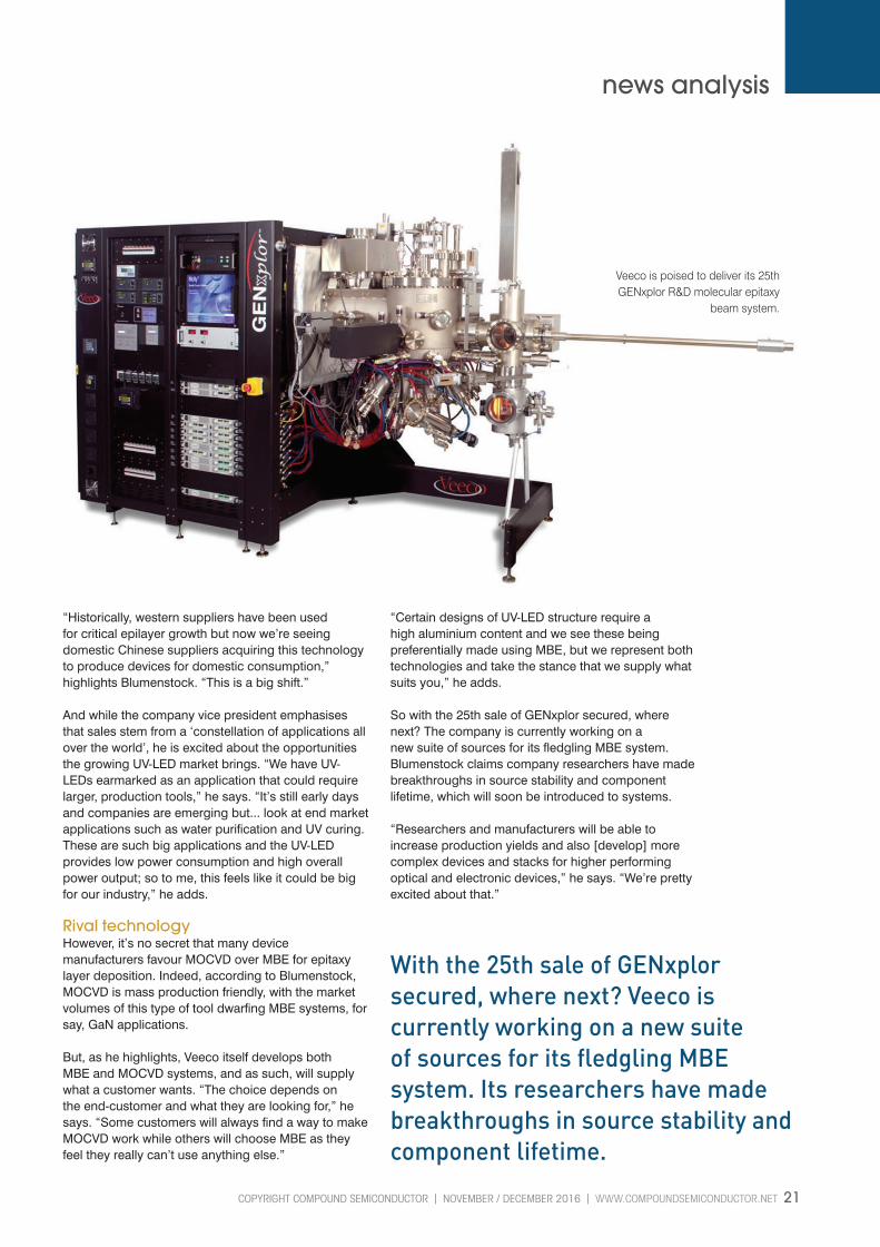
Veeco is poised to deliver its 25th GENxplor R&D molecular epitaxy
beam system.
News Analysis v6MGRS.indd 21 28/11/2016 12:58

Five key themes: £ Refining handset architectures for the 2020’s£ Perfecting Power Electronics£ Optimising Light Emitters£ Revolutionising RF Chips£ Exploiting Heterogenous Integration
Within each topic there is a key-note presentation from one of the most influential companies within this sector; one talk by a leading market analyst who will discuss trends within the industry and presentations by the leaders of firms developing cutting-edge technology in this field.
Connecting, informing and inspiring the compound semiconductor industry.
SPEAKERS ANNOUNCED!CS International 2017 will provide timely, comprehensive coverage of every
important sector within the compound semiconductor industry.
Book your place NOW !www.cs-international.net/register to secure your place
FIVE KEY THEMES LIE AT THE HEART OF CS INTERNATIONAL 2017
The 7th CS International conference will be held at the Sheraton Brussels Airport Hotel, in Belgium on Tuesday 7 & Wednesday 8 March 2017.
CS International will build on the success of its predecessors, including the leaders of the world’s biggest chipmakers and the most promising start-ups providing 30 presentations spanning 5 key themes.
Together, these talks will detail breakthroughs in device technology; offer insights into the current status and the evolution of compound semiconductor devices; and provide
details of advances in tools and processes that will help to drive up fab yields and throughputs. Attendees at this two-day conference will gain an up-to-date overview of the status of the CS industry, and have many opportunities to meet many other key players within this community.
Book your place now. Limited spaces available
CS 2017 Speakers DPS 420 x 297 v21.indd 2 28/11/2016 11:01

This two day event covers fi ve themes
Refi ning Handset Architectures for the 2020’s
Will handsets be crammed with ever more III-V content? Could GaN appear in the front-end in the coming years?
KEYNOTE
£ Stephen Kovacic: Skyworks Solutions I Taking the front-end into the 2020’s
£ Dylan Kelly: Murata Manufacturing I Topic to be announced
ANALYST
£ Eric Higham: Strategy Analytics I The foundry of the 2020’s
Exploiting Heterogenous Integration
What are the fruits of a marriage between silicon and the III-Vs? And can higher mobility materials improve microprocessors and memory?
KEYNOTE
£ Daniel Green: Defence Advanced Research Projects Agency – US Agency of Defence I Advancing technology with heterogeneous integration
SPEAKERS
£ Soon-Fatt Yoon: Nanyang Technological University I Heterogeneous integration of III-V devices on silicon with ultra-thin buffer utilising interfacial misfi t dislocations
£ Jesús A Del Alamo: Microsystems Technology Laboratories I Refi ning the III-V fi nFET
£ Nadine Collaert: imec I Looking for the ultimate low-power switch: the promise of tunnel FETs
£ Jean Fompeyrine: IBM I Advancing SRAM by adding III-Vs (COMPOSE project)
£ Shengkai Wang: Institute of Microelectronics of Chinese Academy of Sciences I III-Vs and germanium for future logic
£ Arnaud Furnemont: imec I 3D NAND scaling: an opportunity for alternative channel material
£ Gerard Colston: Advanced Epi Materials & Devices I Silicon Carbide heteroepitaxy for mass production of semiconductor devices
CS 2017 Speakers DPS 420 x 297 v21.indd 3 28/11/2016 11:01

Revolutionising RF Chips
Will GaN RF deliver the best bang per buck by increasing transistor voltages or making these devices on silicon? And what are the best options for really high frequencies?
KEYNOTE
£ John Palmour: Wolfspeed I GaN-on-SiC RF: Poised for rapid adoption
ANALYST
£ Zhen Zong: Yole Développement I Topic to be announced
SPEAKERS
£ Zach Griffi th: Teledyne Technologies I InP HBTs for high-power 70 to 500 GHz amplifi cation: its status today and where it is going
£ Rocco Giofrè: University of Rome Tor Vergata I GaN Doherty amplifi ers for backhaul radio links
£ Michael Ziehl: MACOM I The virtues of GaN-on-silicon
£ Bernd Heinz: Evatec I Al(1-x)ScxN fi lms for use in RF devices
£ David Danzilio: WIN Semiconductors I Advancing GaA integration
Optimising Light Emitters
Sponsored by JSC Technology Park Pulsar
Are colossal LED fabs revolutionising chip manufacture? And what are the big opportunities for visible lasers?
KEYNOTE
£ Hsu Chen K: Sanan Optoelectronics I Creating the biggest and best LED chipmaker in Chinan
ANALYST
£ Swapna Prakash I Lighting-up India with LEDs
SPEAKERS
£ Oleg Shchekin: Lumileds I Non-linear processes in LEDs and engineering for effi ciency at high power densities
£ Martin Behringer: OSRAM Opto Semiconductors I LED - more than just a light emitting cube
£ Tatsushi Hamaguchi: Sony Corporation I Fulfi lling the promise of the GaN VCSEL
£ Bedwyr Humphreys: Seren Photonics I Overcoming the green gap using semipolar gallium nitride
CS 2017 Speakers DPS 420 x 297 v21.indd 4 28/11/2016 11:01
DELEGATE BAG SPONSOR PORTFOLIO SPONSOR
SUPPORTED BY
LANYARD SPONSOR
All speakers and presentations are subject to change. ©2016 Angel Business Communications Ltd.
GOLD SPONSORS
PLATINUM SPONSORS
Perfecting Power Electronics
Can the best devices stem from the ultra-wide bandgap of gallium oxide? Or will they emerge from foundries processing GaN and SiC on silicon?
KEYNOTE
£ Toshimi Hitora: FLOSFIA I Unleashing the potential of gallium oxide
SPEAKERS
£ Tamara Baksht: VisIC Technologies I High efficiency at high power density: realization of GaN’s promise for power electronics
£ Frédéric Dupont: Exagan I Driving the GaN power device roadmap for large scale adoption
£ Isik Kizilyalli: US. Department of the Energy Advanced Research Project Agency I Current topics in electronic devices based on wide band-gap semiconductors for power applications and energy efficiency
£ Sujit Banerjee: Monolith Semiconductor ISlashing chip costs with SiC-on-silicon
£ Anthony Sagneri: FINsix Corporation I Wide bandgap devices: the key to the world’s smallest laptop charger
£ Markus Behet: EpiGaN I From Hype to Reality: GaN/Si - where are we today?
£ John Palmour: Wolfspeed I Topic to be announced
WIFI SPONSOR
CS 2017 Speakers DPS 420 x 297 v21.indd 5 28/11/2016 11:01
26 WWW.COMPOUNDSEMICONDUCTOR.NET l NOVEMBER / DECEMBER 2016 l COPYRIGHT COMPOUND SEMICONDUCTOR
interview SiC industry
The shifting
SiC landscapeRichard Stevenson talks to IHS Markit analyst Richard Eden about the big events in the SiC industry, such as Infineon’s plans to purchase Wolfspeed, X-Fab’s establishing of a 150 mm SiC foundry, and the acquisition of Fairchild by ON Semiconductor.
SiC interview v6MGRS.indd 26 28/11/2016 12:51

COPYRIGHT COMPOUND SEMICONDUCTOR l NOVEMBER / DECEMBER 2016 l WWW.COMPOUNDSEMICONDUCTOR.NET 27
interview SiC industry
Q Within the SiC industry, this year will be remembered for the buying of Wolfspeed, essentially Cree’s SiC division, by European electronics giant Infineon. As the first to bring the SiC diode to market, Infineon is already a leader in this technology. So what is the rationale behind its aim to buy Wolfspeed in a cash deal worth $850 million?
A There are two main reasons. Firstly, although Infineon is a big player in the SiC diode market, it’s way behind Cree and others when it comes to the potentially larger SiC MOSFET market. After several years of pushing its SiC JFETs, it only finally launched the SiC MOSFET earlier this year. So it’s four or five years behind the curve for SiC MOSFETs. By acquiring Wolfspeed, it will immediately get a product range that is established, which has gone through several design optimisations, and is already in mass production. So it can get market share.
The other key element in the Wolfspeed acquisition is that Infineon obtains the world- leading substrate wafer production capacity, and its know-how. It gives Infineon in-house control of the essential resource to make its own wafers, and it saves costs from having to buy wafers from a commercial source.
Q Will this acquisition make Europe the leader of SiC power devices, given that STMicroelectronics also produces SiC diodes and MOSFETs based on this material?
A To some extent, yes. Control of Wolfspeed’s product development will shift across the Atlantic to Europe. But I don’t think that they’ll move the actual production or design engineering for a long time yet.
Q How does the sale of Wolfspeed impact the US? Is General Electric now the local leader of this technology?
A I think General Electric is probably one of the most well-known American companies, but there are plenty of other American companies that are active in the SiC market, maybe some smaller ones. GeneSiC, Global Power Technology Group, Microsemi, Northrop Grumman, Raytheon and United Silicon Carbide are all deeply involved, and you have new companies like Monolith Semiconductor.
Q In the Asia-Pacific region, is Rohm still the leading manufacturer of SiC power devices?
A Yes, I think so. But Rohm is unusual [in this region], in that it sells all of its SiC products commercially. It has no captive, internal market making end-equipment, whereas some of the other Japanese and Asian companies that produce SiC products do so for internal use in their finished end equipment. Selling [the SiC products] is a side line. For those companies, examples would be Denso, Fuji Electric, Hitachi, Mitsubishi Electric, Toshiba, Toyota and so on.
Q ON Semiconductor has just bought Fairchild for $2.4 billion. Back in 2011, Fairchild equipped itself with SiC BJT technology by buying TranSiC. Do you think ON Semiconductor will continue to promote this technology?
A No, I don’t, because Fairchild stopped developing the SiC-based BJTs in around 2014. However, ON Semiconductor will continue to invest in wide bandgap materials, maintaining both companies’ strategies. Fairchild had already announced SiC diodes, developed by the former TranSiC team in Sweden, with its SiC MOSFETs coming soon: this work will continue unchanged. ON Semi was working with GaN, in partnership with Transphorm, as well as an in-house GaN project: these will also continue. Q Does the acquisition of SiC start-ups such as SemiSouth and TranSiC, and the multi- million dollar acquisitions on Wolfspeed and Fairchild, suggest that there is no longer a place for the little guy in the SiC power industry?
A No, there are still several little guys left in the SiC industry. For example, Anvil Semiconductors in the UK, Ascatron in Sweden, and then a host of companies in America – small guys: BASiC 3C, GeneSiC, Global Power Technology Group, Monolith Semiconductor, and United Silicon Carbide. They may have strategies to be bought eventually, but they all want to be big companies. They are all ambitious.
Q Have all the world’s leading silicon power device makers now got SiC technology, either through acquisition or in-house development?
SiC interview v6MGRS.indd 27 28/11/2016 12:51

28 WWW.COMPOUNDSEMICONDUCTOR.NET l NOVEMBER / DECEMBER 2016 l COPYRIGHT COMPOUND SEMICONDUCTOR
interview SiC industry
A I’d say no, but I would say that the ones who are not involved in SiC are probably working on GaN. The likes of Alpha & Omega Semiconductor, NXP, Panasonic and Texas Instruments are only involved in GaN. Even Vishay – which has has historically bought up companies involved in older, established technologies – is developing a 650 V discrete, normally-off GaN power transistor in-house. This has not been formerly or officially announced, but this news was quietly displayed on the Vishay booth at Electronica. Expect plans to be announced in Q1 ‘17.
Q Do these electronics giants see SiC power devices as complementary to their silicon products, or as eventual successors?
A In general, it’s a mix of both. Overall, they are hedging their bets, so they have an income stream in future, whichever way the market moves. In the short term it will be complementary, but in the long term it may be a successor – so they have got to be in that market, or their sales will just dry up.
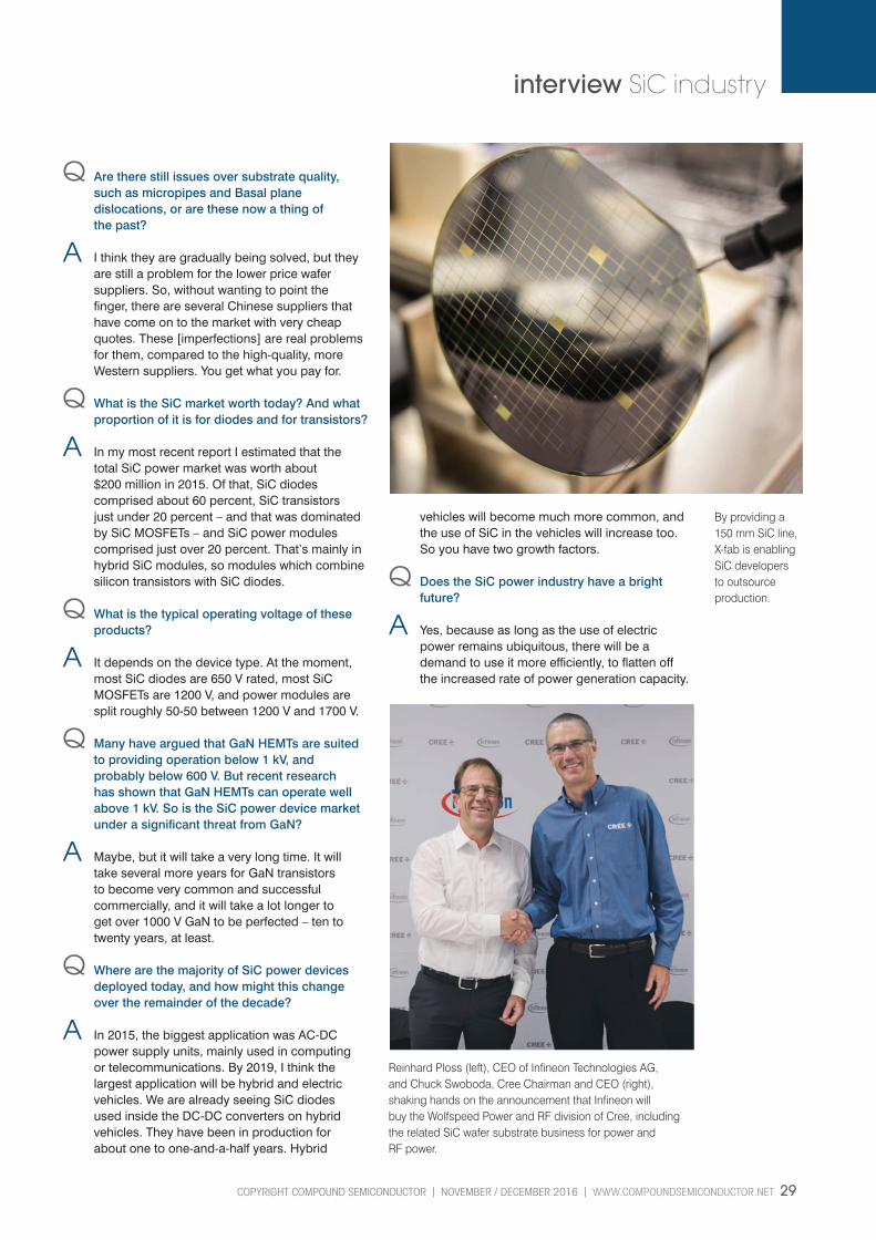
Q X-fab is developing a 6-inch SiC line that will enable companies to outsource their chip production. Do you expect this move to have a big impact on the industry?
A I think it may have an impact, but I don’t know how big it will be. It certainly enables the prospect of fabless SiC companies to spring up. When I spoke to X-fab last, they said that they had already got about five signed-up clients for the SiC foundry service. It’s probably increased a bit since then.
Q How would you describe the level of maturity of the SiC diode and transistor today? And what flavour of transistor is most popular?
A I’d say that for SiC diodes, and to some extent SiC transistors, you don’t hear about the solving of performance or reliability problems anything like as much as you did four or five years ago. So it’s definitely maturing, but there is still some room to improve further.
In terms of the flavour of transistor, SiC MOSFETs are definitely the transistor of choice of end customers, even though there are benefits to both SiC JFETs and SiC BJTs.
The market choice is driven by perception, not by the laws of physics. Engineers have been designing with normally off silicon MOSFETs for about 30 years, so they want a SiC alternative that is driven in a similar way; a technology that they are comfortable with.
Q Is there any appetite for the commercialisation of other SiC power devices, such as a thyristor?
A Not that I’ve seen.
Q How will Infineon’s purchase of Wolfspeed impact the SiC substrate market?
A As Infineon will get full control of its SiC substrate manufacturing process, it can optimise the characteristic it wants for its products. It can allocate production to suit its needs as well.
I believe that Cree was the biggest supplier of wafers in the SiC power market, so Infineon may be able to control which of its competitors it supplies – if any. So I think the likes of Dow Corning, II-VI Incorporated and SiCrystal will be rubbing their hands, because the market- leading competitor may be about to exit the market.
Q Dow Corning has strived to take a bigger share of the SiC substrate market. Has it made much ground so far, or does Wolfspeed currently dominate the substrate market?
A I think Wolfspeed, or Cree, has still been the dominant supplier in the market up until now. I know Dow Corning has tried hard, and has caught Cree heavily, but I don’t think they have overtaken them.
Q Is the manufacture of SiC chips shifting to larger substrates?
A Yes, but slowly. The market is still using 100 mm diameter wafers at the moment, but it is actively transitioning to 150 mm wafers. In my most recent report, published in February this year, I estimated the use of 150 mm wafers would overtake 100 mm by 2018.
By the end of this decade, the biggest market for SiC devices is expected to switch from power supplies to electric and hybrid electric vehicles.
SiC interview v6MGRS.indd 28 28/11/2016 12:52
COPYRIGHT COMPOUND SEMICONDUCTOR l NOVEMBER / DECEMBER 2016 l WWW.COMPOUNDSEMICONDUCTOR.NET 29
interview SiC industry
Q Are there still issues over substrate quality, such as micropipes and Basal plane dislocations, or are these now a thing of the past?
A I think they are gradually being solved, but they are still a problem for the lower price wafer suppliers. So, without wanting to point the finger, there are several Chinese suppliers that have come on to the market with very cheap quotes. These [imperfections] are real problems for them, compared to the high-quality, more Western suppliers. You get what you pay for.
Q What is the SiC market worth today? And what proportion of it is for diodes and for transistors?
A In my most recent report I estimated that the total SiC power market was worth about $200 million in 2015. Of that, SiC diodes comprised about 60 percent, SiC transistors just under 20 percent – and that was dominated by SiC MOSFETs – and SiC power modules comprised just over 20 percent. That’s mainly in hybrid SiC modules, so modules which combine silicon transistors with SiC diodes.
Q What is the typical operating voltage of these products?
A It depends on the device type. At the moment, most SiC diodes are 650 V rated, most SiC MOSFETs are 1200 V, and power modules are split roughly 50-50 between 1200 V and 1700 V.
Q Many have argued that GaN HEMTs are suited to providing operation below 1 kV, and probably below 600 V. But recent research has shown that GaN HEMTs can operate well above 1 kV. So is the SiC power device market under a significant threat from GaN?
A Maybe, but it will take a very long time. It will take several more years for GaN transistors to become very common and successful commercially, and it will take a lot longer to get over 1000 V GaN to be perfected – ten to twenty years, at least.
Q Where are the majority of SiC power devices deployed today, and how might this change over the remainder of the decade?
A In 2015, the biggest application was AC-DC power supply units, mainly used in computing or telecommunications. By 2019, I think the largest application will be hybrid and electric vehicles. We are already seeing SiC diodes used inside the DC-DC converters on hybrid vehicles. They have been in production for about one to one-and-a-half years. Hybrid
vehicles will become much more common, and the use of SiC in the vehicles will increase too. So you have two growth factors.
Q Does the SiC power industry have a bright future?
A Yes, because as long as the use of electric power remains ubiquitous, there will be a demand to use it more efficiently, to flatten off the increased rate of power generation capacity.
By providing a 150 mm SiC line, X-fab is enabling SiC developers to outsource production.
Reinhard Ploss (left), CEO of Infineon Technologies AG, and Chuck Swoboda, Cree Chairman and CEO (right), shaking hands on the announcement that Infineon will buy the Wolfspeed Power and RF division of Cree, including the related SiC wafer substrate business for power and RF power.
SiC interview v6MGRS.indd 29 28/11/2016 12:52
30 WWW.COMPOUNDSEMICONDUCTOR.NET l NOVEMBER / DECEMBER 2016 l COPYRIGHT COMPOUND SEMICONDUCTOR
technology III-V CMOS
III-V CMOS transistors on 300 mm silicon for logic applications
FOR THE LAST FIVE DECADES, the semiconductor industry has successfully benefited from the miniaturization of the MOSFET. The dimensions of transistors have been continuously scaled to meet the requirements for high performance and low power consumption as demanded by application.
Today, the semiconductor industry faces many serious challenges for extending Moore’s law beyond the 10 nm technology node. One of these challenges is to increase the transistor density, while keeping total power density under control through a scaling of the operating voltage. Unfortunately, reducing the operating voltage has unwanted consequences, impacting device performance and impairing switching speed.
One modification that can be made to the MOSFET is to replace the silicon channel with a high-mobility material, such as III-V compounds. This adjustment has the potential to enhance the on-state current, especially at low supply voltages of 0.5 V or less,
due to better carrier transport properties at low electric fields. This allows the III-V channel to show great potential in low-power, high-performance applications. However, monolithic integration of III-Vs on large-scale silicon wafers is a significant challenge.
Recently, several approaches have been used to successfully integrate InGaAs with silicon substrates. Examples include: direct epitaxy of III-V on 300 mm silicon, using a strain-relaxed buffer layer or aspect ratio trapping; direct wafer bonding; and template-assisted selective epitaxy. All these approaches are aiding the development of high quality III-V channel transistors on silicon.
At the Taiwan Semiconductor Manufacturing Company, we are playing our part in this pursuit of III-V MOSFETs by fabricating InGaAs transistors on 300 mm silicon substrates for low-voltage logic applications. To do this we have studied the epitaxial growth of the InGaAs channel, the deposition of a high-κ gate dielectric, and source/drain contact
InGaAs MOSFETs, and in general III-V on 300 mm silicon, remain channel materials of interest for future technology application
BY MAO-LIN HUNAG, SHANG-WEN CHANG, CHUN-HSIUNG LIN, HOWARD C.-H. WANG, AND CARLOS H. DIAZ FROM TAIWAN SEMICONDUCTOR MANUFACTURING COMPANY
TSMC v7MGRS.indd 30 28/11/2016 12:50

COPYRIGHT COMPOUND SEMICONDUCTOR l NOVEMBER / DECEMBER 2016 l WWW.COMPOUNDSEMICONDUCTOR.NET 31
technology III-V CMOS
resistance; and we have evaluated transistor architectures and characteristics.
Epitaxy of the InGaAs channelGrowth of a high-quality InGaAs epi-layer can be realized on 300 mm, on-axis silicon (100) wafers with a strain-relaxed buffer layer technology. The 8 percent lattice-mismatch between silicon and In0.53Ga0.47As can be accommodated by two metamorphic buffer layers, which minimize crystalline defects at the top InGaAs channel.
Formation of the strain-relaxed structure begins with the growth of a GaAs layer directly on a silicon substrate, followed by an InP buffer layer to gradually relax the misfit strain. Growth of an In0.52Al0.48As back barrier follows, and then an In0.53Ga0.47As channel, which is lattice-matched to InP.
All these III-V layers are grown by MOCVD, a technology that delivers high throughput production and has the capability for selective area growth.
Figure 1. Transmission electron microscopy images of III-V epitaxial layers grown on a 300 mm silicon substrate. (a) III-V/silicon heterostructures including a silicon substrate, strain-relaxed buffer layers, back barrier, and channel. (b) Top InGaAs channel. (M.L. Huang et. al. VLSI Symp. Tech. Dig. 2015)
TSMC v7MGRS.indd 31 28/11/2016 12:50
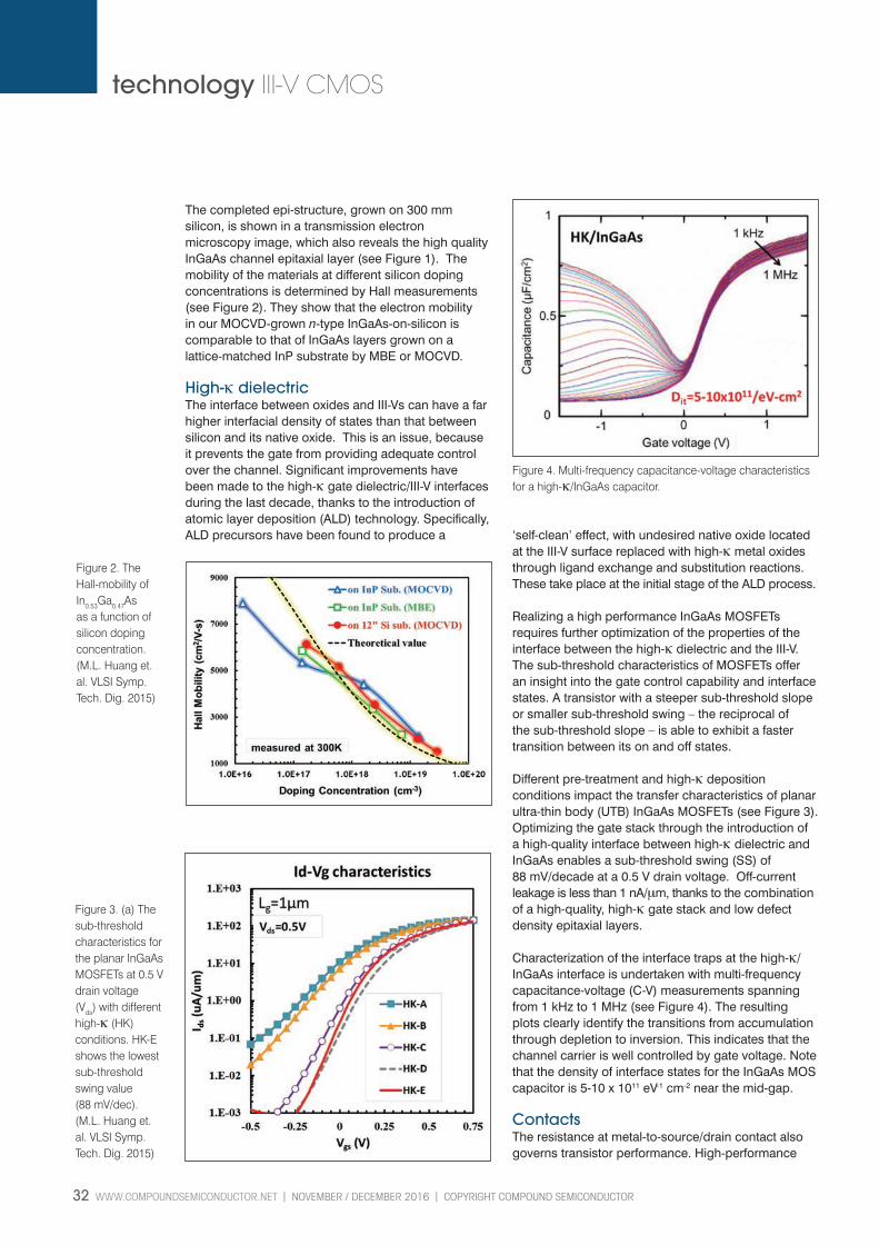
32 WWW.COMPOUNDSEMICONDUCTOR.NET l NOVEMBER / DECEMBER 2016 l COPYRIGHT COMPOUND SEMICONDUCTOR
technology III-V CMOS
Figure 2. The Hall-mobility of In0.53Ga0.47As as a function of silicon doping concentration. (M.L. Huang et. al. VLSI Symp. Tech. Dig. 2015)
Figure 3. (a) The sub-threshold characteristics for the planar InGaAs MOSFETs at 0.5 V drain voltage (Vds) with different high-κ (HK) conditions. HK-E shows the lowest sub-threshold swing value (88 mV/dec). (M.L. Huang et. al. VLSI Symp. Tech. Dig. 2015)
The completed epi-structure, grown on 300 mm silicon, is shown in a transmission electron microscopy image, which also reveals the high quality InGaAs channel epitaxial layer (see Figure 1). The mobility of the materials at different silicon doping concentrations is determined by Hall measurements (see Figure 2). They show that the electron mobility in our MOCVD-grown n-type InGaAs-on-silicon is comparable to that of InGaAs layers grown on a lattice-matched InP substrate by MBE or MOCVD.
High-κ dielectricThe interface between oxides and III-Vs can have a far higher interfacial density of states than that between silicon and its native oxide. This is an issue, because it prevents the gate from providing adequate control over the channel. Significant improvements have been made to the high-κ gate dielectric/III-V interfaces during the last decade, thanks to the introduction of atomic layer deposition (ALD) technology. Specifically, ALD precursors have been found to produce a
Figure 4. Multi-frequency capacitance-voltage characteristics for a high-κ/InGaAs capacitor.
‘self-clean’ effect, with undesired native oxide located at the III-V surface replaced with high-κ metal oxides through ligand exchange and substitution reactions. These take place at the initial stage of the ALD process.
Realizing a high performance InGaAs MOSFETs requires further optimization of the properties of the interface between the high-κ dielectric and the III-V. The sub-threshold characteristics of MOSFETs offer an insight into the gate control capability and interface states. A transistor with a steeper sub-threshold slope or smaller sub-threshold swing – the reciprocal of the sub-threshold slope – is able to exhibit a faster transition between its on and off states.
Different pre-treatment and high-κ deposition conditions impact the transfer characteristics of planar ultra-thin body (UTB) InGaAs MOSFETs (see Figure 3). Optimizing the gate stack through the introduction of a high-quality interface between high-κ dielectric and InGaAs enables a sub-threshold swing (SS) of 88 mV/decade at a 0.5 V drain voltage. Off-current leakage is less than 1 nA/μm, thanks to the combination of a high-quality, high-κ gate stack and low defect density epitaxial layers.
Characterization of the interface traps at the high-κ/InGaAs interface is undertaken with multi-frequency capacitance-voltage (C-V) measurements spanning from 1 kHz to 1 MHz (see Figure 4). The resulting plots clearly identify the transitions from accumulation through depletion to inversion. This indicates that the channel carrier is well controlled by gate voltage. Note that the density of interface states for the InGaAs MOS capacitor is 5-10 x 1011 eV-1 cm-2 near the mid-gap.
ContactsThe resistance at metal-to-source/drain contact also governs transistor performance. High-performance
TSMC v7MGRS.indd 32 28/11/2016 12:50

Untitled-3 1 28/11/2016 15:41
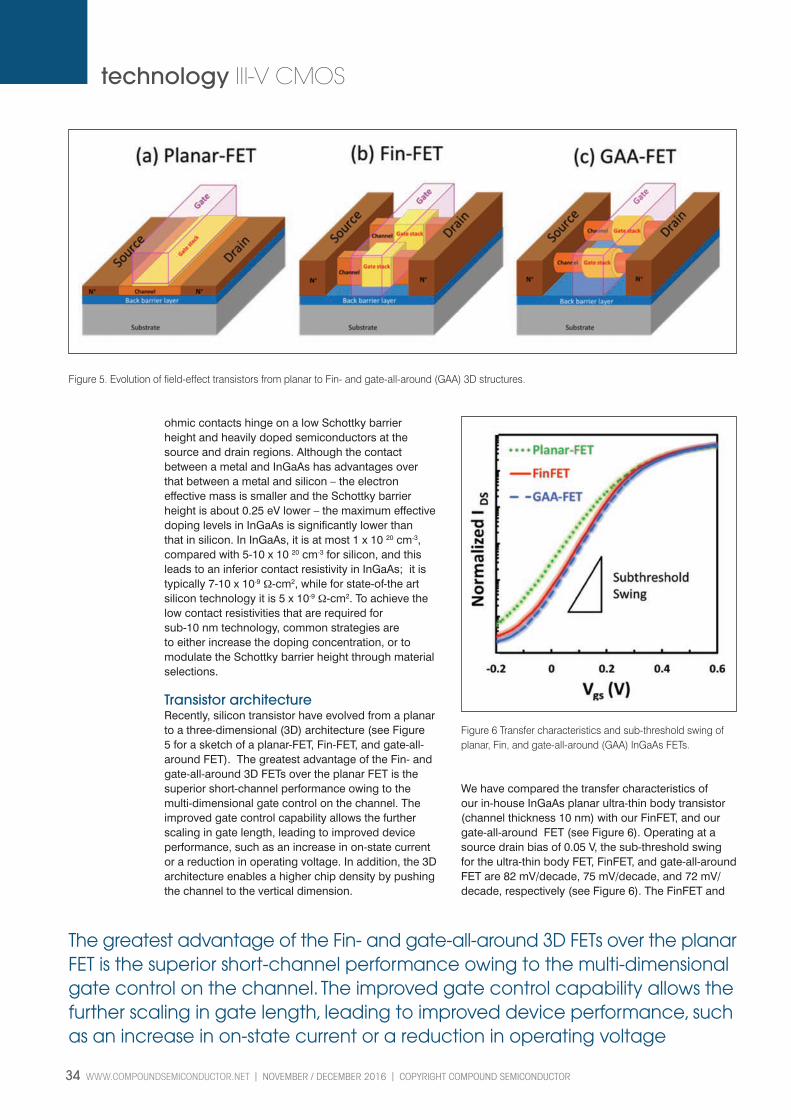
34 WWW.COMPOUNDSEMICONDUCTOR.NET l NOVEMBER / DECEMBER 2016 l COPYRIGHT COMPOUND SEMICONDUCTOR
technology III-V CMOS
ohmic contacts hinge on a low Schottky barrier height and heavily doped semiconductors at the source and drain regions. Although the contact between a metal and InGaAs has advantages over that between a metal and silicon – the electron effective mass is smaller and the Schottky barrier height is about 0.25 eV lower – the maximum effective doping levels in InGaAs is significantly lower than that in silicon. In InGaAs, it is at most 1 x 10 20 cm-3, compared with 5-10 x 10 20 cm-3 for silicon, and this leads to an inferior contact resistivity in InGaAs; it is typically 7-10 x 10-9 Ω-cm2, while for state-of-the art silicon technology it is 5 x 10⁻⁹ Ω-cm2. To achieve the low contact resistivities that are required for sub-10 nm technology, common strategies are to either increase the doping concentration, or to modulate the Schottky barrier height through material selections.
Transistor architecture Recently, silicon transistor have evolved from a planar to a three-dimensional (3D) architecture (see Figure 5 for a sketch of a planar-FET, Fin-FET, and gate-all-around FET). The greatest advantage of the Fin- and gate-all-around 3D FETs over the planar FET is the superior short-channel performance owing to the multi-dimensional gate control on the channel. The improved gate control capability allows the further scaling in gate length, leading to improved device performance, such as an increase in on-state current or a reduction in operating voltage. In addition, the 3D architecture enables a higher chip density by pushing the channel to the vertical dimension.
We have compared the transfer characteristics of our in-house InGaAs planar ultra-thin body transistor (channel thickness 10 nm) with our FinFET, and our gate-all-around FET (see Figure 6). Operating at a source drain bias of 0.05 V, the sub-threshold swing for the ultra-thin body FET, FinFET, and gate-all-around FET are 82 mV/decade, 75 mV/decade, and 72 mV/decade, respectively (see Figure 6). The FinFET and
Figure 5. Evolution of field-effect transistors from planar to Fin- and gate-all-around (GAA) 3D structures.
Figure 6 Transfer characteristics and sub-threshold swing of planar, Fin, and gate-all-around (GAA) InGaAs FETs.
The greatest advantage of the Fin- and gate-all-around 3D FETs over the planar FET is the superior short-channel performance owing to the multi-dimensional gate control on the channel. The improved gate control capability allows the further scaling in gate length, leading to improved device performance, such as an increase in on-state current or a reduction in operating voltage
TSMC v7MGRS.indd 34 28/11/2016 12:50
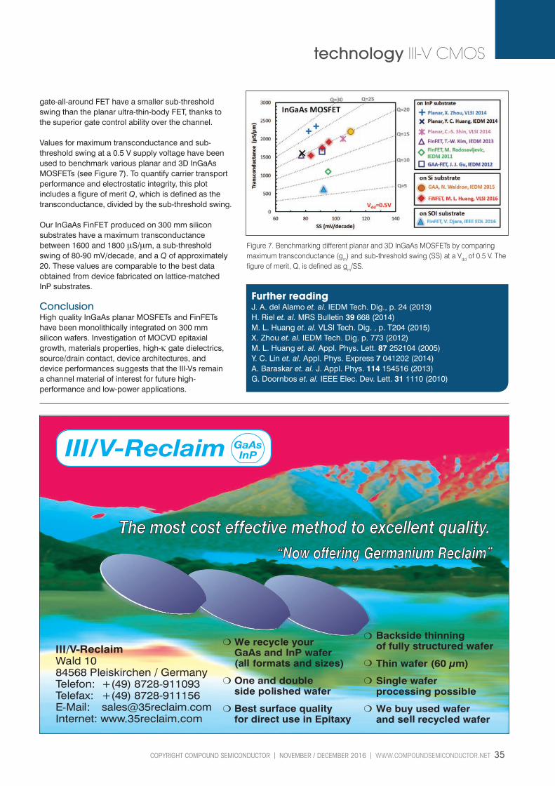
COPYRIGHT COMPOUND SEMICONDUCTOR l NOVEMBER / DECEMBER 2016 l WWW.COMPOUNDSEMICONDUCTOR.NET 35
technology III-V CMOS
Figure 7. Benchmarking different planar and 3D InGaAs MOSFETs by comparing maximum transconductance (gm) and sub-threshold swing (SS) at a Vdd of 0.5 V. The figure of merit, Q, is defined as gm/SS.
Further readingJ. A. del Alamo et. al. IEDM Tech. Dig., p. 24 (2013)H. Riel et. al. MRS Bulletin 39 668 (2014)M. L. Huang et. al. VLSI Tech. Dig. , p. T204 (2015)X. Zhou et. al. IEDM Tech. Dig. p. 773 (2012)M. L. Huang et. al. Appl. Phys. Lett. 87 252104 (2005)Y. C. Lin et. al. Appl. Phys. Express 7 041202 (2014)A. Baraskar et. al. J. Appl. Phys. 114 154516 (2013)G. Doornbos et. al. IEEE Elec. Dev. Lett. 31 1110 (2010)
gate-all-around FET have a smaller sub-threshold swing than the planar ultra-thin-body FET, thanks to the superior gate control ability over the channel.
Values for maximum transconductance and sub-threshold swing at a 0.5 V supply voltage have been used to benchmark various planar and 3D InGaAs MOSFETs (see Figure 7). To quantify carrier transport performance and electrostatic integrity, this plot includes a figure of merit Q, which is defined as the transconductance, divided by the sub-threshold swing.
Our InGaAs FinFET produced on 300 mm silicon substrates have a maximum transconductance between 1600 and 1800 μS/μm, a sub-threshold swing of 80-90 mV/decade, and a Q of approximately 20. These values are comparable to the best data obtained from device fabricated on lattice-matched InP substrates.
ConclusionHigh quality InGaAs planar MOSFETs and FinFETs have been monolithically integrated on 300 mm silicon wafers. Investigation of MOCVD epitaxial growth, materials properties, high-κ gate dielectrics, source/drain contact, device architectures, and device performances suggests that the III-Vs remain a channel material of interest for future high-performance and low-power applications.
“Now offering Germanium Reclaim”
TSMC v7MGRS.indd 35 28/11/2016 12:50

Creating and strengthening links between chipmakers and network builders
2nd PIC International Conference SPEAKERS ANNOUNCED!
PIC International 2017 will provide timely, comprehensive coverage of every important sector within the photonic integrated circuits industry.
Book your place NOW !www.picinternational.net/register
TWO DAYS, FIVE THEMES
Sales of PICs are soaring, with their deployment helping to boost the capacity of networks and data centres. To aid this industry, we are strengthening the relationships between the makers and the users of these integrated circuits by organising the 2nd PIC International, a global conference dedicated to this industry.
In 2017, the conference grows to a new auditorium to welcome more industry leaders and rising stars driving the next generation of photonic integrated circuits.
Key themes include a deep dive into PIC platforms, manufacturing solutions, device deployment in data centres, telecoms and a full update on activity in emerging markets such as life sciences.
“Over two days, PIC International gives you an incredibly valuable perspective on what it takes to realise the benefits of
integrated optoelectronic devices, and I think that’s why this conference has captured the imagination of the photonics community, ” added James Tyrrell, Programme Manager for the 2017 show. Just like in 2016, the event is co-located with CS International to bring you the best of the compound semiconductor industry. Also, we’ve matched the scheduling to make it even easier for delegates to jump between tracks and pick the speaker session that suits you best.
Join us at the Sheraton Brussels Airport Hotel, in Belgium on Tuesday 7 & Wednesday 8 March 2017.
Book your place now. Limited spaces available
LANYARD SPONSOR
SUPPORTED BY
PLATINUM SPONSORS
WIFI SPONSOR
GOLD SPONSORS
PIC 2017 Speakers DPS 420 x 297 v20.indd 2 25/11/2016 16:00

All speakers and presentations are subject to change. ©2016 Angel Business Communications Ltd.
This two day event covers five themesLeveraging PICs in long-haul and metro networks
How can PICs support traffic growth? And how can they deliver value to operators?
KEYNOTE £ Geoff Bennett: Infinera co-presenting with Eric Loos: BICS An in-depth look at the deployment of PIC technology in long haul networks, and a perspective on future application
SPEAKERS£ Mehrdad Ziari: Infinera Large scale coherent PICs in optical networks£ Vladimir Kozlov: LightCounting Market Research Impact of integrated photonics on the optical communications market£ Martin Guy: Ciena Corporation Strategies for photonic integration for metro and long-haul networks£ Tom Williams: Acacia Communications Inc. Putting silicon photonics to work on metro and long haul applications£ Le Binh: Huawei Technologies Integrated photonics systems to meet challenges in optical and wireless system convergence£ Michael Wale: Oclaro Technology PIC-enabled telecommunications and data centre interconnects: state of the art and future prospects
Supporting Data Centre Growth
Short reach communications could be a major win for PICs. But what are the customer priorities? And how can photonic integrated circuits come out on top?
KEYNOTE £ Richard Pitwon – Seagate Technology Opportunities for data centre optical interconnects
SPEAKERS£ James Regan: EFFECT Photonics InP as a platform for photonic integration£ Karen Liu: Kaiam Corporation Perspectives on hybrid integration as a rapid and flexible route to upgrading today’s datacenters£ Bert Jan Offrein: IBM Scalable integration concepts to drive down the cost of data centre photonics£ Robert Blum: Intel Corporation Silicon photonics and the future of optical connectivity in the data centre£ Jörg-Peter Elbers: ADVA Optical Networking Silicon photonics for inter-data centre interconnects
PIC Platforms
What are the key materials systems driving photonic integration? And how should these platforms evolve to unlock greater performance?
KEYNOTE£ Graham Reed: University of Southampton Ion implantation of Ge into silicon to form photonics devices
SPEAKERS£ Roel Baets: Ghent University Silicon photonics beyond transceivers
£ Timo Aalto: VTT Research Thick-SOI for PICs and I/O coupling£ Dimitris Tsiokos: Phosnet Research Group, Aristotle University of Thessaloniki CMOS compatible plasmo-photonics for mass- manufactured, powerful PICs£ Michael Geiselmann: LiGenTec Applications for thick film silicon nitride integrated circuits£ Arne Leinse: LioniX International TriPleX™: The low loss industrial silicon nitride waveguide platform. Application examples from VIS to IR£ Zhihong Huang: Hewlett Packard Enterprise Silicon photonics as a PIC platform for next generation atacentre architectures£ Martin Schell: Fraunhofer HHI Is plastic fantastic? Learnings from polymer hybrid and InP monolithic integration
Optimising PIC Design, Manufacturing & Packaging
What are the best resources for creating and delivering photonic integrated circuits?
KEYNOTE£ Michael Watts: MIT Bringing resources together to drive photonic integration
SPEAKERS£ Peter O’Brien: Tyndall National Institute Overcoming packaging hurdles for PIC devices£ Suresh Venkatesan: POET Technologies Realizing gains in energy efficiency, component cost and size-reduction through photonic integrated solutions£ Peter de Dobbelaere: Luxtera The design and processing of advanced transceiver integrated circuits£ Gilles Lamant: Cadence Design Systems Providing mainstream design flow for PICs£ André Richter: VPIphotonics Advances in layout-aware schematic-driven design automation for integrated photonic and optoelectronics£ Niek Nijenhuis: PhoeniX Software PhoeniX Software’s unique position in the photonic IC landscape£ Ignazio Piacentini: ficonTEC Testing as part of the manufacturing chain: photonics wafers, singulated dies, and fully packaged devices
New markets: Sensing, Medical?
What are the prospects for developers more broadly? And how does the supply chain need to adapt?
KEYNOTE £ Liesbet Lagae: imecimec’s progress as the pix4life project in the field of SiN photonics in the visible range for life science applications
SPEAKERS£ Pim Kat: Technobis Group Extreme fibre sensing: PIC opportunities beyond datacoms and telecoms£ Iain McKenzie: European Space Agency PICs: The final frontier£ Ewit Roos: Photon Delta Why European photonics is undervalued and a fast-track plan of how to change it
PIC 2017 Speakers DPS 420 x 297 v20.indd 3 25/11/2016 16:00
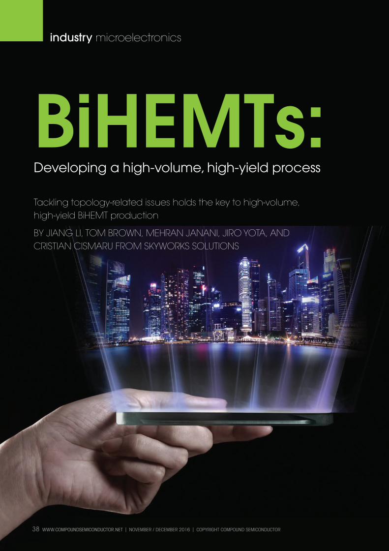
38 WWW.COMPOUNDSEMICONDUCTOR.NET l NOVEMBER / DECEMBER 2016 l COPYRIGHT COMPOUND SEMICONDUCTOR
industry microelectronics
BiHEMTs: Developing a high-volume, high-yield process
Tackling topology-related issues holds the key to high-volume, high-yield BiHEMT production
BY JIANG LI, TOM BROWN, MEHRAN JANANI, JIRO YOTA, AND CRISTIAN CISMARU FROM SKYWORKS SOLUTIONS
Skyworks v7RS.indd 38 28/11/2016 12:51
COPYRIGHT COMPOUND SEMICONDUCTOR l NOVEMBER / DECEMBER 2016 l WWW.COMPOUNDSEMICONDUCTOR.NET 39
industry microelectronics
SMARTPHONES are delivering staggering levels of performance. These marvelous devices can stream videos with great resolution, provide music on the move, take great pictures, and run a vast number of applications.
To accomplish all of this and more, numerous components are crammed together on a very small footprint. So there is great pressure to reduce the real estate of every part, including the power amplifier that enables communication between the handset and the base station.
The dominant transistor technology for the power amplifier is the InGaP/GaAs HBT. It delivers excellent RF performance in a reproducible manner, and it is manufactured in high volumes with a high yield. However, when this chip is deployed in advanced frond-end modules, it fails to meet RF designer’s zero-size requirements. Given this state of affairs, there is a compelling need to integrate the HBT with a FET or a pHEMT on the same chip, because this aids design flexibility and circuit functionality while reducing the module’s size and its overall cost.
One option for forming a single GaAs chip that integrates either the FET or the pHEMT with the HBT is to insert the FET into the emitter section of the HBT. Compared to a HBT-only process, the strengths of the resulting BiFET are a low epitaxial cost, shared process steps, and minimal impact on production cycle time. But there are also weaknesses – as the FET and HBT have shared layers, optimization of the device is hampered; and the BiFET has poor RF isolation.
The alternative approach is to vertically stack the pHEMT underneath the HBT sub-collector. This creates a BiHEMT, a device that features an absence of shared layers between the pHEMT and the HBT. Thanks to this independence, it is possible to individually optimize the thickness and doping within each device. Additional merits are good device RF performance and isolation, resulting from the integration of the pHEMT underneath the HBT sub-collector, so that it is positioned on top of the semi-insulated substrate.
However, all these advantages must be weighed against the big structure topology, which makes the fabrication of the BiHEMT more challenging. It is particularly demanding to develop a sub-micron pHEMT gate process that ensures good RF device performance.
At Skyworks Solutions we have pursued the second of the two options for device integration, successfully developing an advanced BiHEMT technology that stacks the pHEMT underneath the InGaP/GaAs HBT
sub-collector. To enable commercial success, we have identified and addressed many fabrication challenges. This has led to high volume, high-yield manufacture of GaAs BiHEMTs on our 6-inch production line.
Forming BiHEMT epiwafers is straightforward, involving the growth of the HBT epitaxial structure on top of the pHEMT. Using MOCVD, HEMT epitaxial layers are deposited on 150 mm semi-isolating GaAs substrates, before the highly doped HBT sub-collector is added, followed by the collector, base, and emitter layers.
We have introduced slight modifications to our HBT layer stack to accommodate the implementation of the pHEMT underneath the HBT. This includes the optimization of the HBT sub-collector thickness, in order to reduce the overall BiHEMT topology. The electric performance of the HBT is not compromised by this adjustment.
Additional changes are to insert etch stop layers for process robustness (see Table 1 for the InGaP/GaAs BiHEMT epitaxial structure), and to take special care
Figure 1. The BiHEMT has a severe device topology, so its production requires optimized processes to prevent yield from taking a hit.
Table 1. One of the key advantages of the BiHEMT over the BiFET is that it enables the optimization of every layer within the epitaxial structure.
Skyworks v7RS.indd 39 28/11/2016 12:51

40 WWW.COMPOUNDSEMICONDUCTOR.NET l NOVEMBER / DECEMBER 2016 l COPYRIGHT COMPOUND SEMICONDUCTOR
industry microelectronics
during HBT layer growth. These refinements minimize the possibility of degrading pHEMT performance.
To fabricate the BiHEMT, we use many conventional processes (details are provided in the box “Making a BiHEMT”). Compared to the standard HBT-only process, the additional process challenges for making the BiHEMT are primarily associated with the severe topology created by the combination of active devices, passive components, metal interconnections, and dielectric layers. There is a step height of about 2 μm between the top of the HBT emitter contact and the pHEMT gate layer at the bottom (see Figure 1).
Topography challengesDue to this substantial height difference, it is critical to optimize the photo and etch processes for gate formation, so that the pHEMT gate Schottky layer is
opened and etched with good uniformity and process control. These processes need to be reliable and provide a good process margin, to prevent wafer scrap that leads to increased loss and inferior yield.
We found that with our BiHEMT production process, the gate metal can be missing after gate lift-off (see Figure 2). Investigations revealed that the missing gate is more common at the reticle corner, due to a combination of a non-optimized gate photo process and non-optimized photo process tool conditions.
To find a solution to the missing gate issue, we introduced a novel method to pre-screen the gate yield. Implementation occurred at the post gate metal formation step, before completion of the process and the process control monitoring test.
This approach revealed that prior to optimization of gate photolithography, yield loss could be as high as almost 20 percent (See Figure 3 (a)). But gate integrity yields of 99 percent are now possible, by optimizing specific gate photo exposure conditions, equipment tuning and mask modification. These steps eliminate missing gate issue in the reticle corner (see Figure 3 (b)).
Another stumbling block to establishing a high-volume, high-yield BiHEMT process is the erosion of photoresist in the thin film TaN resistor process. Again, this is a topology-related process.
Formation of the TaN resistors, which are located at the pHEMT level, begins with a photolithography process to pattern the resistors. Dry etching of SiN follows, and then TaN deposition to achieve a clean
Figure 2. The pHEMT at the reticle corner is missing a gate, due to high topology/thick gate photo resist and a gate photo exposure that is out of focus.
Figure 3. (a) Gate integrity yield loss due to missing gates was typically seen at reticle field corners. (b) An optimized process ensures gate integrity yield after gate metal lift-off process.
Skyworks v7RS.indd 40 28/11/2016 12:51
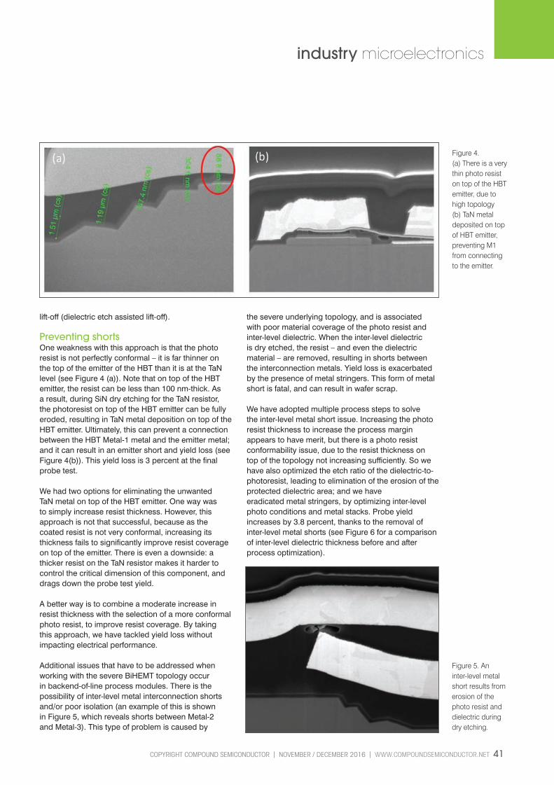
COPYRIGHT COMPOUND SEMICONDUCTOR l NOVEMBER / DECEMBER 2016 l WWW.COMPOUNDSEMICONDUCTOR.NET 41
industry microelectronics
lift-off (dielectric etch assisted lift-off).
Preventing shortsOne weakness with this approach is that the photo resist is not perfectly conformal – it is far thinner on the top of the emitter of the HBT than it is at the TaN level (see Figure 4 (a)). Note that on top of the HBT emitter, the resist can be less than 100 nm-thick. As a result, during SiN dry etching for the TaN resistor, the photoresist on top of the HBT emitter can be fully eroded, resulting in TaN metal deposition on top of the HBT emitter. Ultimately, this can prevent a connection between the HBT Metal-1 metal and the emitter metal; and it can result in an emitter short and yield loss (see Figure 4(b)). This yield loss is 3 percent at the final probe test.
We had two options for eliminating the unwanted TaN metal on top of the HBT emitter. One way was to simply increase resist thickness. However, this approach is not that successful, because as the coated resist is not very conformal, increasing its thickness fails to significantly improve resist coverage on top of the emitter. There is even a downside: a thicker resist on the TaN resistor makes it harder to control the critical dimension of this component, and drags down the probe test yield.
A better way is to combine a moderate increase in resist thickness with the selection of a more conformal photo resist, to improve resist coverage. By taking this approach, we have tackled yield loss without impacting electrical performance.
Additional issues that have to be addressed when working with the severe BiHEMT topology occur in backend-of-line process modules. There is the possibility of inter-level metal interconnection shorts and/or poor isolation (an example of this is shown in Figure 5, which reveals shorts between Metal-2 and Metal-3). This type of problem is caused by
the severe underlying topology, and is associated with poor material coverage of the photo resist and inter-level dielectric. When the inter-level dielectric is dry etched, the resist – and even the dielectric material – are removed, resulting in shorts between the interconnection metals. Yield loss is exacerbated by the presence of metal stringers. This form of metal short is fatal, and can result in wafer scrap.
We have adopted multiple process steps to solve the inter-level metal short issue. Increasing the photo resist thickness to increase the process margin appears to have merit, but there is a photo resist conformability issue, due to the resist thickness on top of the topology not increasing sufficiently. So we have also optimized the etch ratio of the dielectric-to-photoresist, leading to elimination of the erosion of the protected dielectric area; and we have eradicated metal stringers, by optimizing inter-level photo conditions and metal stacks. Probe yield increases by 3.8 percent, thanks to the removal of inter-level metal shorts (see Figure 6 for a comparison of inter-level dielectric thickness before and after process optimization).
Figure 4. (a) There is a very thin photo resist on top of the HBT emitter, due to high topology (b) TaN metal deposited on top of HBT emitter, preventing M1 from connecting to the emitter.
Figure 5. An inter-level metal short results from erosion of the photo resist and dielectric during dry etching.
Skyworks v7RS.indd 41 28/11/2016 12:51

42 WWW.COMPOUNDSEMICONDUCTOR.NET l NOVEMBER / DECEMBER 2016 l COPYRIGHT COMPOUND SEMICONDUCTOR
industry microelectronics
Making a BiHEMTProduction of the BiHEMT begins with the formation of the emitter contact. Photolithography defines the HBT emitter pattern, and emitter contact metal evaporation and lift-off follow. There is no need to employ an emitter alloy, because emitter metal contacts are deposited on a highly doped emitter top layer.
A combination of photolithography and an inductively coupled plasma dry etch, which stops on top of the InGaP HBT emitter layer, defines the emitter mesa. This pair of processes is also used to form the base pedestal. Deposition of a SiN film by PECVD provides protection to the HBT active area, while access to the pHEMT layers comes from wet-etching of the sub-collector layer.
Formation of the HBT base contact involves etching of the SiN film and the InGaP layer, metal deposition and liftoff; the HBT collector contact is defined by deposition of AuGeNi/Au and subsequent rapid thermal processing. The pHEMT source and drain ohmic contacts are formed simultaneously with the HBT collector. Devices, diodes, and other passive components are electrically isolated by helium ion implantation, and the pHEMT gate defined by photolithography, gate recess wet etch, Ti/Pt/Au gate metal deposition and lift-off.
Following formation of the intrinsic HBT and the pHEMT, devices are passivated by PECVD of SiN films. The next steps involve the fabrication of TaN thin film resistors, metal-to-metal SiN capacitors, inductors and metal interconnects. The front side process for the BiHEMT is completed with final passivation, resulting from SiN deposition. Figure 7. Optimizing processes for BiHEMT production lead to
a high die-sort yield, according to data accumulated from over 6 million units.
Figure 6. Dielectric erosion improvement comparison. (a) Before process optimization, the dielectric between Metal-1 and Metal-2 is too thin, causing poor isolation between M1 and M2; (b) Following process optimization, there is good isolation between M1 and M2, thanks to eradication of dielectric material erosion.
To determine the performance provided by our BiHEMTs, we have undertaken DC and RF testing. The results are encouraging: HBT performance is comparable to that of our HBT-only technology, while the required RF performance for various circuit applications is provided by the pHEMT.
Realizing a high-yield in BiHEMT technology is not simply a matter of optimizing multiple process
modules – it also relies critically on testability and test coverage in die-sort. To this end, we have over 60 parameters that are recorded in a DC test for process control monitoring, and over 50 parameters are probed in final test step.
Armed with these results, while implementing our processes that address all the topology-related process issues, we can realize a probe die-sort yield in BiHEMT technology that consistently exceeds 95 percent in our high-volume production line (see Figure 7).
That’s good news for engineers making smartphones, as they can now get what they crave – power amplifiers that combine great performance with a tiny footprint.
£ The authors wish to thank the contributions provided by Ravi Ramanathan, Mike Sun and Manjeet Singh of Skyworks Solutions.
Skyworks v7RS.indd 42 28/11/2016 12:51

Untitled-1 1 07/11/2016 09:38

44 WWW.COMPOUNDSEMICONDUCTOR.NET l NOVEMBER / DECEMBER 2016 l COPYRIGHT COMPOUND SEMICONDUCTOR
technology LEDs
The world’s first monolithic
full-colour LEDUltra-high-resolution flexible displays will benefit from microLEDs that efficiently emit all three primary colours
BY JYH-CHIA CHEN, MILTON YEH AND HUSSEIN S. EL-GHOROURY FROM OSTENDO TECHNOLOGY INC.
Ostendo v4RS.indd 44 28/11/2016 12:53
COPYRIGHT COMPOUND SEMICONDUCTOR l NOVEMBER / DECEMBER 2016 l WWW.COMPOUNDSEMICONDUCTOR.NET 45
technology LEDs
THERE ARE FUNDAMENTAL FLAWS with both of the leading approaches for producing LED-based white light sources and full-colour displays. If white light is formed from the colour mixing of separate red, green and blue LEDs that are packaged together as one device, the resulting unit must combine red LEDs made from AlGaInP with GaN-based green and blue emitters – and pairing these different types of LED requires special efforts, due to substantial differences in electrical characteristics and material properties. With the main alternative, there are also major downsides. In this case, a blue LED is coated with a yellow phosphor, and white light results from colour mixing. Efficiency is then compromised, due to cascade losses that occur during the blue-to-yellow colour conversion of the photons.
In addition to these drawbacks, both of these approaches are held back by basic issues related to the source, including a high packaging cost, low efficiency, a large device size, low yield and poor reliability. What’s needed, but not commercially available, is a single device that emits all the three primary colours of light.
Progress in this direction has been made by several teams, including Korean electronics giant Samsung. It has produced GaN-based, pyramid-shaped LEDs that emit multiple wavelengths simultaneously to create a white-light source. However, these devices cannot emit all three primary colours independently, so while they are suitable for lighting applications, they can’t be used for displays.
An alternative approach that is pursued by Zetian Mi’s group at McGill University is to produce monolithic red-green-blue LEDs from nanowire structures. Using a three-step selective-area growth technique, these researchers form three sets of nanowire structures on three different regions. Several wafer preparations are used before and after each selective growth. With this approach, each display pixel is capable of producing the three primary colours, which are emitted from three areas, or sub-pixels. This architecture compromises the pixel dimension of the display, and ultimately its resolution.
Addressing this limitation is our team from Ostendo Technology Inc. of Carlsbad, CA, which has created the world’s first LED that delivers controllable, tuneable full-colour emission through adjustments in current flow. Note that in addition to the three primary colours, our device produces other colours through colour-mixing techniques.
An incredibly important aspect of our technology is that it involves a growth process that is identical to that used for commercial, single-color LEDs – there is no additional pre- or post-growth process. Thanks to this, our technology is practical, and can be scaled to high-volumes and low costs.
Full-colour designUnlike conventional III-nitride LEDs, we use a different quantum well section for each primary colour. Between these sections are specially-designed intermediate carrier blocking layers, made from AlGaN layers with different thicknesses and dopant concentrations (see Figure 1 for a cross-sectional view of our monolithic, three-colour InGaN-based LED).
We have found that the intermediate carrier blocking layers play a key role in controlling the transport and distribution of the carriers across the active region. Careful selection of the thickness, composition and dopant concentration of each of the intermediate carrier blocking layers enables control of the transport of electrons and holes under various current injection conditions. Thanks to this, electrons and holes can be directed into quantum wells that lead to emission at specific dominate wavelengths. Our monolithic LEDs are grown by MOCVD, using a close-coupled shower-head reactor, on c-plane (0001) sapphire substrates. They comprise: a 2 μm-thick, undoped GaN layer; a 3 μm-thick, highly silicon-doped n-type GaN layer; an InGaN compliance layer, inserted for quality improvement purposes; blue InGaN/GaN multi-quantum wells emitting at 460 nm, which contain three 3 nm-thick In0.15Ga0.85N wells separated by 10 nm-thick InGaN barriers; a green-emitting section producing 530 nm emission from three 3 nm-thick In0.25Ga0.75N quantum wells separated by 10 nm-thick InGaN barriers; a region producing red, 650 nm emission from a single 3 nm-thick In0.35Ga0.65N well sandwiched between 10 nm-thick
Ostendo v4RS.indd 45 28/11/2016 12:53
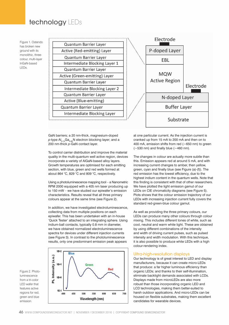
46 WWW.COMPOUNDSEMICONDUCTOR.NET l NOVEMBER / DECEMBER 2016 l COPYRIGHT COMPOUND SEMICONDUCTOR
technology LEDs
GaN barriers; a 20 nm-thick, magnesium-doped p-type Al0.15Ga0.85N electron blocking layer; and a 200 nm-thick p-GaN contact layer.
To control carrier distribution and improve the material quality in the multi-quantum well active region, devices incorporate a variety of AlGaN-based alloy layers. Growth temperatures are optimised for each emitting section, with blue, green and red wells formed at about 864 °C, 829 °C and 809 °C, respectively.
Using a photoluminescence mapping tool – a Nanometric RPM 2000 equipped with a 405 nm laser producing up to 150 mW – we have studied our epiwafer’s emission characteristics. Results reveal that all three primary colours appear at the same time (see Figure 2).
In addition, we have investigated electroluminescence, collecting data from multiple positions on each epiwafer. This has been undertaken with an in-house ‘Quick Tester’ attached to an integrating sphere. Using indium-ball contacts, typically 0.8 mm in diameter, we have obtained normalized electroluminescence spectra for devices under different injection currents (see Figure 3). In contrast to the photoluminescence results, only one predominant emission peak appears
at one particular current. As the injection current is cranked up from 15 mA to 200 mA and then on to 400 mA, emission shifts from red (~650 nm) to green (~530 nm) and finally blue (~460 nm).
The changes in colour are actually more subtle than this. Emission appears red at around 5 mA, and with increasing current changes to amber, then yellow, green, cyan and finally blue (see Figure (a)-(f)). The red emission has the lowest efficiency, due to the highest indium content in the quantum wells. Note that this finding is consistent with that of other researchers. We have plotted the light emission gamut of our LEDs on CIE chromaticity diagrams (see Figure 5). Plots shows that the colour emission trajectory of our LEDs with increasing injection current fully covers the standard red-green-blue colour gamut.
As well as providing the three primary colours, our LEDs can produce many other colours through colour mixing. This includes different tones of white, such as cool, neutral and warm white light. These are obtained by using different combinations of the intensity and width of driving current pulses, such as pulsed intensity and width modulation. With this technique, it is also possible to produce white LEDs with a high colour-rendering index.
Ultra-high-resolution displaysOur technology is of great interest to LED and display manufacturers, because it can create micro-LEDs that produce: a far higher luminous efficiency than organic LEDs; and thanks to their self-illumination, eliminate backlight demands associated with LCDs. Displays made from microLEDs are also more robust than those incorporating organic LED and LCD technologies, making them better-suited to harsh outdoor applications. And micro-LEDs can be housed on flexible substrates, making them excellent candidates for wearable devices.
Figure 1. Ostendo has broken new ground with its monolithic, three-colour, multi-layer InGaN-based LEDs.
Figure 2. Photo-luminescence from a tri-color LED wafer that features active regions for red, green and blue emission.
Ostendo v4RS.indd 46 28/11/2016 12:53

COPYRIGHT COMPOUND SEMICONDUCTOR l NOVEMBER / DECEMBER 2016 l WWW.COMPOUNDSEMICONDUCTOR.NET 47
technology LEDs
Figure 5. The light emission gamut (CIE chromaticity diagrams) from full-colour LED structures.
One group that has made significant strides with displays employing microLED arrays is that of Kei May Lau and co-workers from Hong Kong University of Science and Technology. This team recently demonstrated a micro-display with a resolution of 1700 pixels-per-inch that features micro-LED arrays integrated on silicon CMOS substrates. This micro-display has the potential to serve many applications, such as active driving of pico-projectors, augmented reality, head-up displays in cars, and headsets for gaming. However, the work by this group has been limited to blue light of differing intensity. Turning to our LEDs, and using them in combination with the bonding-on-silicon technology, would enable full-colour displays, without adding any complexity to device fabrication.
Bigger, flexible displaysAs well as being a key building block in micro-displays, the micro-LED has emerged as an important component for future flexible lighting and displays. For examples, John Rogers’ group at the University of Illinois, Urbana-Champaign, has shown that this class of LED can be attached to plastic substrates using micro-transfer printing. This technique has tremendous potential for the production of large-scale, thin and flexible lighting.
One of the merits of printing is that it can slash manufacturing costs by eliminating individual device packaging. What’s more, the small, distributed micro-LEDs can be passively cooled, due to their small size, enabling operation at higher current densities. And last, but by no means least, quantum efficiency can increase through better cooling and superior light extraction, due to the greater surface area and surface scattering. Other techniques that have been actively pursued for the realization of large-area lighting and displays include pick-and-place, ink-jet printing, self-assembly and screen printing of micro-LEDs. So far, the majority of these demonstrations have involved monochromatic light, or white-emission from blue LEDs and a yellow phosphor. Full-colour displays require a more complicated process to precisely place red, green and blue LEDs within the same display.
Manufacturing costs will rise, and resolution could be sacrificed. However, if our approach to making full-colour LEDs is adopted, it will avoid additional manufacturing steps and not compromise resolution.
In short, we believe that our novel, InGaN-based LED technology that incorporates intermediate blocking layers will deliver a significant reduction in the fabrication complexity of full-colour micro-displays. In addition, it will allow large-scale flexible displays to be realized that can compete favourably with existing organic LED technology. We are now developing our technology for displays, which will also be a game changer for next-generation lighting, due to its efficiency, compactness, simplicity and robustness.
Figure 3. Normalized electroluminescence spectra of devices under different injection currents.
Figure 4.(a)-(f). Full colour emission under different injection currents.
Further readingH. S. El-Ghoroury et. al. AIP Advances 6 075316 (2016)H. S. El-Ghoroury et. al. Display Week 2015 (San Jose, California) 371R. Wang et. al. Optics Express 22 A1768 (2014)W. Chong et. al. Compound Semiconductor Integrated Circuit Symposium (CSICs), IEEE (2014)H. Kim et al. Proceedings of the National Academy of Sciences USA 108 10072 (2011)
Ostendo v4RS.indd 47 28/11/2016 12:53

48 WWW.COMPOUNDSEMICONDUCTOR.NET l NOVEMBER / DECEMBER 2016 l COPYRIGHT COMPOUND SEMICONDUCTOR
technology power electronics
Reducing initial failures in GaN-on-GaN vertical diodesEradicating epi-layer growth pits in GaN-on-GaN diodes boosts yield by reducing failures associated with low breakdown voltages
BY FUMIMASA HORIKIRI FROM SCIOCS
THE GaN SEMICONDUCTOR device market is on the rise. GaN-on-SiC devices are gaining traction in RF applications, such as cellular base stations, and power devices based on GaN-on-silicon are starting to make a commercial impact.
However, although both of the devices are better than their silicon rivals, they are not optimal for GaN. That’s because they are hampered by their lateral structure, which is formed by hetero-epitaxial growth of GaN-based layers on SiC or silicon substrates.
Figure 1. Freestanding, 7-inch GaN substrates can be fabricated by HVPE. The dislocation density is uniformly less than 2 × 106 cm-2, while variation in the c-axis direction is the same as that for conventional smaller substrates. The connecting interfaces, which have a high dislocation density, account for just 0.2 percent of the substrate’s area.
A far more promising architecture is that of the GaN-on-GaN vertical device. It has the potential to form a key component in highly efficient power-conversion systems by combining an extremely low specific differential on-resistance with a high breakdown voltage.
At SCIOCS, which was formed in 2015 and has Sumitomo Chemical as the 100 percent shareholder, we have underlined the capability of this vertical chip by developing a very impressive GaN p–n diode. This device, formed on a freestanding GaN substrate by void-assisted separation, combines a record-breaking blocking voltage of 4.7 kV with an on-resistance of just 1.7 mΩ cm2.
To convert the record-breaking device into a great commercial success, it has to be manufactured in high volume with a good yield. But that’s currently challenging on two fronts: there is a lack of availability of large GaN substrates; and the device epilayers are plagued with a high density of pits, which lead to low breakdown voltages. We are tackling both these issues head-on – we are developing larger GaN substrates, which are formed with a novel tiling approach; and we are introducing better growth conditions that slash the epi-pit density.
Building bigger wafers…For the production of GaN devices on freestanding GaN substrates, wafer size is a far bigger issue than it is for the manufacture of lateral GaN devices on SiC and silicon. For freestanding GaN, commercially available substrates have diameters of just 2–4 inches. These small sizes impact the cost of the GaN-on-GaN devices, and when larger wafers are used, there is greater strain and deviation along the c-axis.
One way to overcome these issues is to produce far larger wafers with a tiling technique (see Figure 1). By using HVPE to join multiple hexagonal-seed, void-assisted-separation GaN substrates, we have produced 7-inch GaN substrates. They have a variation along the c-axis direction that is no more
SCOIS v5RS.indd 48 28/11/2016 12:52

To recognise and highlight key industry achievements in advancing photonic integration through platform development, manufacturing, design, packaging and device characterisation, PIC International magazine is proud to announce its PIC Awards programme. With voting taking place online and presentations made at the PIC International 2017 networking dinner on the evening of March 7 in Brussels, the awards put the spotlight on innovation.
Nominations are open to all companies, individuals and organisations within the PIC community, and we encourage
you all to take part. The awards programme is dedicated to celebrating leading lights in the industry and we would be delighted to hear from you.
The 2017 PIC Industry Awards are NOW OPEN for nominations
Closing date: 9 January 2017
PIC PLATFORMSThis award recognises advances in the development and application of key materials systems driving today’s photonic integrated circuits and providing a stepping stone to future devices. ADVANCES IN MANUFACTURINGEvolution in PIC production is helping to bring a new generation of devices into the market. This category celebrates the success stories so far. ADVANCES IN INTEGRATIONThis award recognises innovative approaches to packing more features into a chip and raising the bar to the next level. DEVICE CHARACTERISATIONAdvances in tools, equipment and measurement know-how are bringing greater insight into chip-level performance; and go hand in hand with gains in device development and production. This award showcases the leading lights in this domain. DESIGN AND PACKAGINGEquipment makers and chip designers are working ever closer to overcome the challenges of turning ideas into practical devices. In this category we celebrate the design and packaging solutions that have overcome major bottlenecks in the sector. LIFETIME ACHIEVEMENT AWARDPioneers in photonic integration have helped make PICs a reality and their knowledge and expertise underpins major advances in the industry. This award recognises outstanding service to the sector.
Nominations are now open and it is FREE to enter.
www.picawards.net
7 MarchSheraton Brussels Airport Hotel, Belgium
PIC Awards 2017 Ad v3.indd 1 21/11/2016 16:07
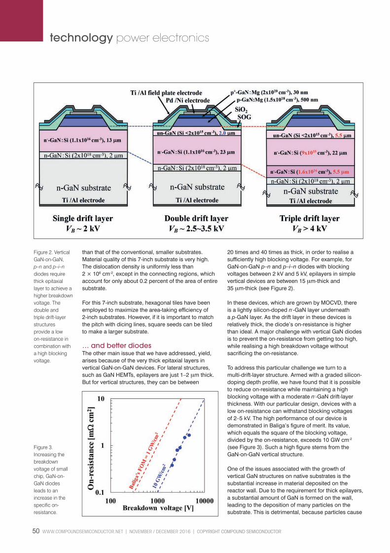
50 WWW.COMPOUNDSEMICONDUCTOR.NET l NOVEMBER / DECEMBER 2016 l COPYRIGHT COMPOUND SEMICONDUCTOR
technology power electronics
than that of the conventional, smaller substrates.Material quality of this 7-inch substrate is very high. The dislocation density is uniformly less than 2 × 106 cm-2, except in the connecting regions, which account for only about 0.2 percent of the area of entire substrate.
For this 7-inch substrate, hexagonal tiles have been employed to maximize the area-taking efficiency of 2-inch substrates. However, if it is important to match the pitch with dicing lines, square seeds can be tiled to make a larger substrate.
… and better diodesThe other main issue that we have addressed, yield, arises because of the very thick epitaxial layers in vertical GaN-on-GaN devices. For lateral structures, such as GaN HEMTs, epilayers are just 1–2 μm thick. But for vertical structures, they can be between
20 times and 40 times as thick, in order to realise a sufficiently high blocking voltage. For example, for GaN-on-GaN p–n and p–i–n diodes with blocking voltages between 2 kV and 5 kV, epilayers in simple vertical devices are between 15 μm-thick and 35 μm-thick (see Figure 2).
In these devices, which are grown by MOCVD, there is a lightly silicon-doped n--GaN layer underneath a p-GaN layer. As the drift layer in these devices is relatively thick, the diode’s on-resistance is higher than ideal. A major challenge with vertical GaN diodes is to prevent the on-resistance from getting too high, while realising a high breakdown voltage without sacrificing the on-resistance.
To address this particular challenge we turn to a multi-drift-layer structure. Armed with a graded silicon-doping depth profile, we have found that it is possible to reduce on-resistance while maintaining a high blocking voltage with a moderate n--GaN drift-layer thickness. With our particular design, devices with a low on-resistance can withstand blocking voltages of 2–5 kV. The high performance of our device is demonstrated in Baliga’s figure of merit. Its value, which equals the square of the blocking voltage, divided by the on-resistance, exceeds 10 GW cm-2 (see Figure 3). Such a high figure stems from the GaN-on-GaN vertical structure.
One of the issues associated with the growth of vertical GaN structures on native substrates is the substantial increase in material deposited on the reactor wall. Due to the requirement for thick epilayers, a substantial amount of GaN is formed on the wall, leading to the deposition of many particles on the substrate. This is detrimental, because particles cause
Figure 2. Vertical GaN-on-GaN, p–n and p–i–n diodes require thick epitaxial layer to achieve a higher breakdown voltage. The double and triple drift-layer structures provide a low on-resistance in combination with a high blocking voltage.
Figure 3. Increasing the breakdown voltage of small chip, GaN-on-GaN diodes leads to an increase in the specific on-resistance.
SCOIS v5RS.indd 50 28/11/2016 12:52
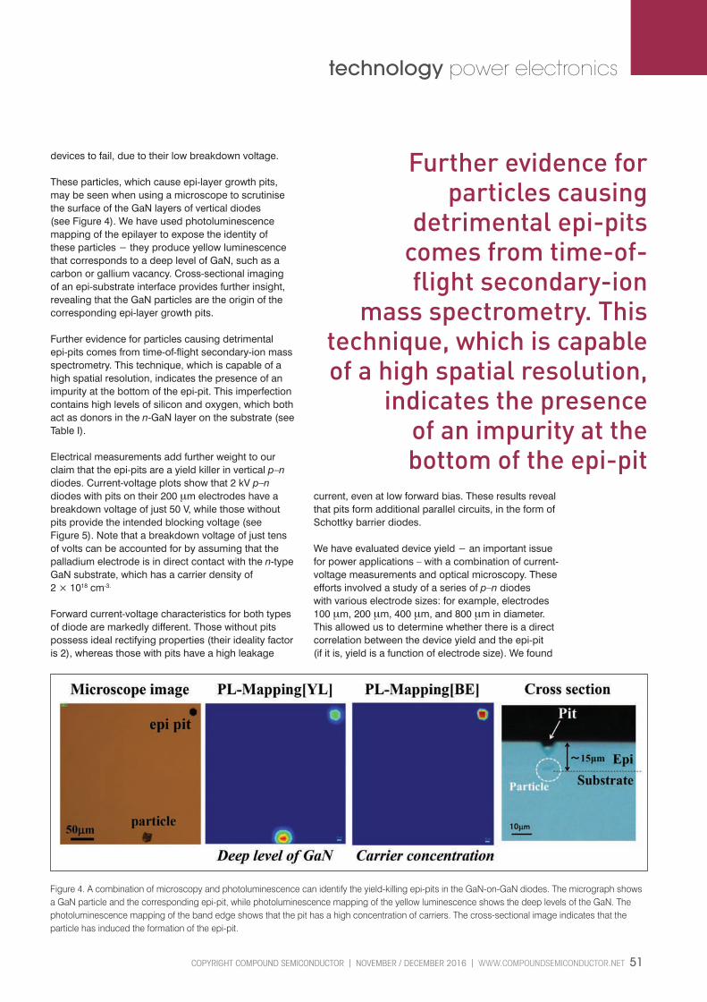
COPYRIGHT COMPOUND SEMICONDUCTOR l NOVEMBER / DECEMBER 2016 l WWW.COMPOUNDSEMICONDUCTOR.NET 51
technology power electronics
devices to fail, due to their low breakdown voltage.
These particles, which cause epi-layer growth pits, may be seen when using a microscope to scrutinise the surface of the GaN layers of vertical diodes (see Figure 4). We have used photoluminescence mapping of the epilayer to expose the identity of these particles − they produce yellow luminescence that corresponds to a deep level of GaN, such as a carbon or gallium vacancy. Cross-sectional imaging of an epi-substrate interface provides further insight, revealing that the GaN particles are the origin of the corresponding epi-layer growth pits.
Further evidence for particles causing detrimental epi-pits comes from time-of-flight secondary-ion mass spectrometry. This technique, which is capable of a high spatial resolution, indicates the presence of an impurity at the bottom of the epi-pit. This imperfection contains high levels of silicon and oxygen, which both act as donors in the n-GaN layer on the substrate (see Table I).
Electrical measurements add further weight to our claim that the epi-pits are a yield killer in vertical p–n diodes. Current-voltage plots show that 2 kV p–n diodes with pits on their 200 μm electrodes have a breakdown voltage of just 50 V, while those without pits provide the intended blocking voltage (see Figure 5). Note that a breakdown voltage of just tens of volts can be accounted for by assuming that the palladium electrode is in direct contact with the n-type GaN substrate, which has a carrier density of 2 × 1018 cm-3.
Forward current-voltage characteristics for both types of diode are markedly different. Those without pits possess ideal rectifying properties (their ideality factor is 2), whereas those with pits have a high leakage
current, even at low forward bias. These results reveal that pits form additional parallel circuits, in the form of Schottky barrier diodes.
We have evaluated device yield − an important issue for power applications – with a combination of current-voltage measurements and optical microscopy. These efforts involved a study of a series of p–n diodes with various electrode sizes: for example, electrodes 100 μm, 200 μm, 400 μm, and 800 μm in diameter. This allowed us to determine whether there is a direct correlation between the device yield and the epi-pit (if it is, yield is a function of electrode size). We found
Figure 4. A combination of microscopy and photoluminescence can identify the yield-killing epi-pits in the GaN-on-GaN diodes. The micrograph shows a GaN particle and the corresponding epi-pit, while photoluminescence mapping of the yellow luminescence shows the deep levels of the GaN. The photoluminescence mapping of the band edge shows that the pit has a high concentration of carriers. The cross-sectional image indicates that the particle has induced the formation of the epi-pit.
Further evidence for particles causing
detrimental epi-pits comes from time-of-flight secondary-ion
mass spectrometry. This technique, which is capable of a high spatial resolution,
indicates the presence of an impurity at the bottom of the epi-pit
SCOIS v5RS.indd 51 28/11/2016 12:52

52 WWW.COMPOUNDSEMICONDUCTOR.NET l NOVEMBER / DECEMBER 2016 l COPYRIGHT COMPOUND SEMICONDUCTOR
technology power electronics
Further readingH. Ohta et. al. IEEE Electron Device Lett. 36 1180 (2015)T. Yoshida et. al. Proc. 18th Int. Conf. on Crystal Growth and Epitaxy, Nagoya Japan, 7–12th August 2016 (2016), Tu1-G06-4K. Matsumoto, Compound Semiconductor Magazine, April&May 2016, p. 22 (2016)
that measured yield depends on the electrode’s size in a manner that confirms that epi-pits are fatal to the initial properties of GaN-on-GaN diodes.
To reduce the density of these killer defects, we have optimized the cleaning of the reactor, the pre-cleaning of the GaN substrate, and the growth conditions. This enabled the production of pit-free GaN-on-GaN wafers with an epi-pit density of less than 0.2 cm-2 (see Figure 6).
This low epi-pit density addresses issues associated with the yield of large-sized, vertically structured GaN-on-GaN power devices, which have a strong future ahead of them, thanks to their great performance and the development of larger GaN substrates. Over the next year or so, we will aid the commercialisation of these GaN-on-GaN epiwafers by improving the epi growth process.
Following the eradication of epi-layer growth pits, we will go on to improve the epi quality. This should
lead to a reduction in electron-trap density and an increase carrier life-time. We also plan to investigate the influence of the substrate off-angle deviation on the dislocation density, which may affect the uniformity and the reliability on vertical GaN-on-GaN devices.
£ This research was supported by the Japan Ministry of the Environment as part of the project Technical Innovation to Create a Future Ideal Society and Lifestyle.
Figure 6. Yield of p–n diodes calculated with the equation Yield= exp(-DAS), where D is the density of killer defects in cm-2, A is the device size in cm2, and S is the ratio of the defect-sensitive area. The experimental data were obtained from the yield of p–n diodes for electrode diameters of 100 μm, 200 μm, 400 μm and 800 μm. The density of killer defects was assumed to be 20 cm-2. This density correlates well with the pit density measured by optical microscopy. A recently produced epitaxial layer showed a pit density of less than 0.2 cm-2.
Table I. Time-of-flight secondary-ion mass spectrometry results around an epi-pit.
Figure 5. Reverse current-voltage characteristics of various 2 kV p–n diodes shows that epi-pits lead to a dramatic reduction in breakdown voltage. The inset shows forward current-voltage characteristics of p–n diodes with and without pits. The micrographs show diodes without the field plate. The size of the pits was approximately 15–20 μm.
SCOIS v5RS.indd 52 28/11/2016 12:52

Speakers include: IHS Markit, Qorvo, CommSolid GmbH, Weightless SIG, IHS Markit Sensors, Advanced Epi Materials and Devices, imec, Intrinsic-ID B.V., Lux Research, Wirepas Pino, oneM2M, Kinetics, The Alliance for Internet of Things Innovation (AIOTI), Texas Instruments Benelux B.V, Evertracker GmbH, Enfucell Oy, Xilinx, IBM Watson, Gemalto, Versasense; and more to come.
www.iotinternational.net
3 events 2 days 1 ticket7 - 8 March 2017Sheraton Brussels Airport Hotel, Belgium
THREE cutting edge complimentary conferences and ONE dedicated exhibition featuring leading players from across the globe.
One ticket will gain access to a 2-day event which will see 3 groups of device makers gathered under one roof.
500+ delegates who can attend any one of the 95 presentations on offer.
87 Industry Speakers CONFIRMED so far.
Connecting, informing and inspiring the compound semiconductor industry
Speakers include: Skyworks, FLOSFIA, VisIC, Exagan, ARPA-E, Monolith, FINsix, Wolfspeed, Sanan Optoelectronics, Philips Lumileds Lighting, OSRAM, Sony, WIN Semiconductors, DARPA, MIT, IBM, Institute of Microelectronics of Chinese Academy of Sciences, Murata Manufacturing, EpiGaN, Seren Photonics, Yole Développement, Teledyne Technologies, University of Rome Tor Vergata, Wolfspeed, MACOM, Evatec, Nanyang Technological University, imec, Aixtron, Ferrotec, Nanotronics, Panasonic, Advanced Epi Materials and Devices.
www.cs-international.net
Speakers include: Infinera, Ciena, Huawei Technologies, Oclaro, Seagate, Intel Corporation, Kaiam, LioniX International, POET Technologies, Luxtera, Cadence Design Systems, University of Southampton, Hewlett Packard Enterprise, Gent University, VTT Technical Research Centre of Finland, Phosnet Research Group - Aristotle University of Thessaloniki, LIGENTEC, Fraunhofer HHI, Tyndall National Institute, VPIphotonics, Technobis group, imec, European Space Agency, PhotonDelta, MIT.
www.picinternational.net
Creating and strengthening links between chipmakers and network builders
REGISTER NOW, AND SECURE YOUR PLACE. REGISTRATION ALLOWS ACCESS TO:CS INTERNATIONAL, PIC INTERNATIONAL AND IOT INTERNATIONAL
Building the IoT: Critical Device-Level Technologies
Book your place now. Limited spaces available
CS PIC IoT Conf Ad 210 x 297 v2.indd 1 25/11/2016 16:03

54 WWW.COMPOUNDSEMICONDUCTOR.NET l NOVEMBER / DECEMBER 2016 l COPYRIGHT COMPOUND SEMICONDUCTOR
technology LEDs
THE REVOLUTION in solid-state lighting is well underway. LEDs bulbs are now shipping in significant volumes, thanks to price tags that are far more competitive than they were just a few years ago.
However, if sales of this class of lighting are to continue to increase, it must not only get cheaper – it must also deliver higher powers and a better colour quality. And that means a fundamental change in the emission process.
The incumbent approach for generating white light involves using GaN-based, blue LEDs to pump phosphors that emit at longer wavelengths. But there are drawbacks with this: the phosphor can curl and delaminate, ruling out the use of such sources for extended periods of time and for providing high-power lighting.
A more promising approach is to colour-mix the emission from an AlGaInP-based red LED with green and blue LEDs made from the III-N material system. This can create a more natural white-light spectra and a higher wall-plug efficiency.
However, if this approach is to fulfil its promise, the green LED must produce a power conversion efficiency of 60 percent or more. Today it’s just half that value, a problem described as the ‘green gap’.
Green LEDs: The case for cubic GaN
Green LEDs formed from cubic GaN can have lower Auger losses, higher hole carrier mobility, greater optical gain and increased p-doping efficiency
BY CAN BAYRAM FROM THE UNIVERSITY OF ILLINOIS AT URBANA-CHAMPAIGN
Researchers have been trying to find a solution to the green gap for more than two decades, and during that time six barriers to higher efficiency have been identified: a high-indium content, a high level of defectivity, low p-doping, carrier asymmetry, polarization and Auger.
All of these six issues plaguing these conventional green LEDs, which employ the hexagonal phase of GaN, have been studied in significant depth. It is well known that the high indium content needed to ensure that InGaN quantum wells emit in the
Cubic GaN v7MGRS.indd 54 28/11/2016 13:00

COPYRIGHT COMPOUND SEMICONDUCTOR l NOVEMBER / DECEMBER 2016 l WWW.COMPOUNDSEMICONDUCTOR.NET 55
technology LEDs
green LED hampers the efficiency of the device, due to a miscibility gap in this alloy; and that the epilayers are riddled with defects, due to lattice- and thermal-mismatch, which arise from growth on foreign substrates, such as sapphire and silicon. In addition, realising a high level of p-doping in nitrides is challenging, due to a high activation energy for the magnesium impurity (it is in excess of 200 meV); there is also a significant asymmetry between electron and hole densities and mobilities, stemming from the large difference between activation energies for p-type and n-type dopants; there are strong internal electric fields within the LED, associated with non-centrosymmetry and inherit piezoelectricity of the hexagonal lattice; and last, but by no means least, Auger non-radiative recombination supresses efficiency at current densities beyond just 10 A cm-2.
Given all these issues, it is clear that the addressing of the green gap requires a technological breakthrough. And one promising solution for this is to turn to polarization-free structures.
Preventing polarizationTo date, efforts at developing polarization-free LEDs have focused on switching from an inherently polar growth plane to one that is inherently polarization-free
Figure 1. Cubic phase III-nitrides might enable a new era for ‘green’ LEDs, thanks to their ~0.2 eV lower bandgap than their hexagonal counterparts.
Cubic GaN v7MGRS.indd 55 28/11/2016 13:00
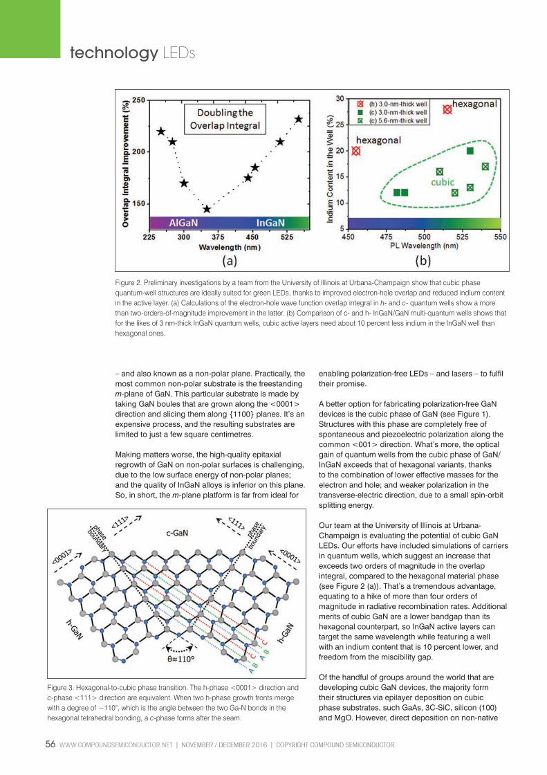
56 WWW.COMPOUNDSEMICONDUCTOR.NET l NOVEMBER / DECEMBER 2016 l COPYRIGHT COMPOUND SEMICONDUCTOR
technology LEDs
– and also known as a non-polar plane. Practically, the most common non-polar substrate is the freestanding m-plane of GaN. This particular substrate is made by taking GaN boules that are grown along the <0001> direction and slicing them along {1100} planes. It’s an expensive process, and the resulting substrates are limited to just a few square centimetres.
Making matters worse, the high-quality epitaxial regrowth of GaN on non-polar surfaces is challenging, due to the low surface energy of non-polar planes; and the quality of InGaN alloys is inferior on this plane. So, in short, the m-plane platform is far from ideal for
enabling polarization-free LEDs – and lasers – to fulfil their promise.
A better option for fabricating polarization-free GaN devices is the cubic phase of GaN (see Figure 1). Structures with this phase are completely free of spontaneous and piezoelectric polarization along the common <001> direction. What’s more, the optical gain of quantum wells from the cubic phase of GaN/InGaN exceeds that of hexagonal variants, thanks to the combination of lower effective masses for the electron and hole; and weaker polarization in the transverse-electric direction, due to a small spin-orbit splitting energy.
Our team at the University of Illinois at Urbana-Champaign is evaluating the potential of cubic GaN LEDs. Our efforts have included simulations of carriers in quantum wells, which suggest an increase that exceeds two orders of magnitude in the overlap integral, compared to the hexagonal material phase (see Figure 2 (a)). That’s a tremendous advantage, equating to a hike of more than four orders of magnitude in radiative recombination rates. Additional merits of cubic GaN are a lower bandgap than its hexagonal counterpart, so InGaN active layers can target the same wavelength while featuring a well with an indium content that is 10 percent lower, and freedom from the miscibility gap.
Of the handful of groups around the world that are developing cubic GaN devices, the majority form their structures via epilayer deposition on cubic phase substrates, such GaAs, 3C-SiC, silicon (100) and MgO. However, direct deposition on non-native
Figure 2. Preliminary investigations by a team from the University of Illinois at Urbana-Champaign show that cubic phase quantum-well structures are ideally suited for green LEDs, thanks to improved electron-hole overlap and reduced indium content in the active layer. (a) Calculations of the electron-hole wave function overlap integral in h- and c- quantum wells show a more than two-orders-of-magnitude improvement in the latter. (b) Comparison of c- and h- InGaN/GaN multi-quantum wells shows that for the likes of 3 nm-thick InGaN quantum wells, cubic active layers need about 10 percent less indium in the InGaN well than hexagonal ones.
Figure 3. Hexagonal-to-cubic phase transition. The h-phase <0001> direction and c-phase <111> direction are equivalent. When two h-phase growth fronts merge with a degree of ~110°, which is the angle between the two Ga-N bonds in the hexagonal tetrahedral bonding, a c-phase forms after the seam.
Cubic GaN v7MGRS.indd 56 28/11/2016 13:00
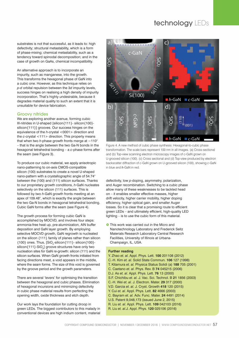
COPYRIGHT COMPOUND SEMICONDUCTOR l NOVEMBER / DECEMBER 2016 l WWW.COMPOUNDSEMICONDUCTOR.NET 57
technology LEDs
substrates is not that successful, as it leads to: high defectivity; structural metastability, which is a form of phase-mixing; chemical metastability, such as a tendency toward spinodal decomposition; and in the case of growth on GaAs, chemical incompatibility.
An alternative approach is to incorporate an impurity, such as manganese, into the growth. This transforms the hexagonal phase of GaN into a cubic one. However, as this technique relies on p-d orbital repulsion between the 3d impurity levels, success hinges on realising a high density of impurity incorporation. That’s highly undesirable, because it degrades material quality to such an extent that it is unsuitable for device fabrication.
Groovy nitridesWe are exploring another avenue, forming cubic III-nitrides in U-shaped [silicon{111}- silicon{100}- silicon{111}] grooves. Our success hinges on the equivalence of the h-crystal <0001> direction and the c-crystal <111> direction. This property means that when two h-phase growth fronts merge at ~110° – that is the angle between the two Ga-N bonds in the hexagonal tetrahedral bonding – a c-phase forms after the seam (see Figure 3).
To produce our cubic material, we apply anisotropic nano-patterning to on-axis CMOS-compatible silicon (100) substrates to create a novel U-shaped nano-pattern with a crystallographic angle of 54.74° between the (100) and (111) silicon surfaces. Thanks to our proprietary growth conditions, h-GaN nucleates selectively on the silicon (111) surfaces. This is followed by two h-GaN growth fronts meeting at an apex of 109.48°, which is exactly the angle between the two Ga-N bonds in hexagonal tetrahedral bonding. Cubic GaN forms after the seam (see Figure 4).
The growth process for forming cubic GaN is accomplished by MOCVD, and involves four steps: ammonia-free heat up, pre-aluminization, AlN buffer deposition and GaN layer growth. By employing selective MOCVD growth, GaN regrowth is nucleated on the silicon {111} family of planes rather than silicon {100} ones. Thus, [SiO2-silicon{111}- silicon{100}- silicon{111}-SiO2] groove structures have only two nucleation sites for GaN re-growth: silicon (111) and the silicon surfaces. When GaN growth fronts initiated from facing directions meet, a void appears in the middle, where the seam forms. The size of this void is governed by the groove period and the growth parameters.
There are several ‘levers’ for optimising the transition between the hexagonal and cubic phases. Elimination of hexagonal incursions and minimizing defectivity in cubic phase material results from perfecting the opening width, oxide thickness and etch depth.
Our work lays the foundation for cutting droop in green LEDs. The biggest contributors to this malady in conventional devices are high indium content, material
defectivity, low p-doping, asymmetry, polarization, and Auger recombination. Switching to a cubic phase allow many of these weaknesses to be tackled head on – it enables smaller effective masses, higher drift velocity, higher carrier mobility, higher doping efficiency, higher optical gain, and smaller Auger losses. So it is clear that a promising route to efficient green LEDs – and ultimately efficient, high-quality LED lighting – is to use the cubic form of this material.
£ This work was carried out in the Micro and Nanotechnology Laboratory and Frederick Seitz Materials Research Laboratory Central Research Facilities, University of Illinois at Urbana- Champaign, IL, USA.
Further readingY. Zhao et. al. Appl. Phys. Lett. 100 201108 (2012)C.-H. Kim et. al. Solid State Commun. 106 127 (1998)T. Kitamura et. al. Physica Status Solidi (a) 188 705 (2001)C. Caetano et. al. Phys. Rev. B 74 045215 (2006)D.J. As et. al. Appl. Phys. Lett. 76 13 (2000)S.F. Chichibu et. al. J. Vac. Sci. Technol. B 21 1856 (2003)C.-H. Wei et. al. J. Electron. Mater. 29 317 (2000)V.D. Garcia et. al. J. Cryst. Growth 418 120 (2015)Y. Cui et. al. Appl. Phys. Lett. 82 4666 (2003)C. Bayram et. al. Adv. Func. Mater. 24 4491 (2014)U.S. Patent 9,048,173 (issued June 2, 2015)R. Liu et. al. Appl. Phys. Lett. 109 042103 (2016)R. Liu et. al.J. Appl. Phys. 120 025106 (2016)
Figure 4. A new method of cubic phase synthesis: Hexagonal-to-cubic phase transformation. The scale bars represent 100 nm in all images. (a) Cross-sectional and (b) Top-view scanning electron microscopy images of c-GaN grown on U-grooved silicon (100). (c) Cross sectional and (d) Top-view produced by electron backscatter diffraction of c-GaN grown on U-grooved silicon (100), showing c-GaN in blue and h-GaN in red.
Cubic GaN v7MGRS.indd 57 28/11/2016 13:00
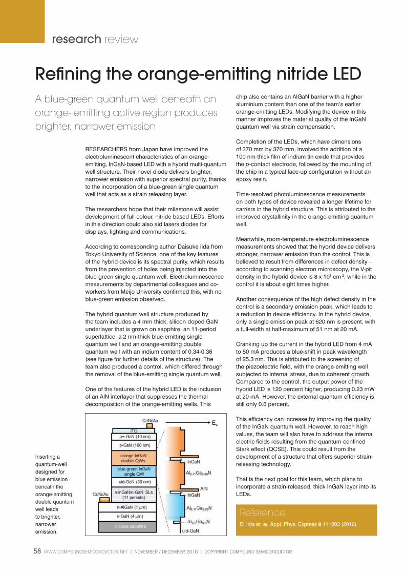
58 WWW.COMPOUNDSEMICONDUCTOR.NET l NOVEMBER / DECEMBER 2016 l COPYRIGHT COMPOUND SEMICONDUCTOR
research review
Refining the orange-emitting nitride LEDA blue-green quantum well beneath an orange- emitting active region produces brighter, narrower emission
ReferenceD. Iida et. al. Appl. Phys. Express 9 111003 (2016)
Inserting a quantum-well designed for blue emission beneath the orange-emitting, double quantum well leads to brighter, narrower emission.
RESEARCHERS from Japan have improved the electroluminescent characteristics of an orange-emitting, InGaN-based LED with a hybrid multi-quantum well structure. Their novel diode delivers brighter, narrower emission with superior spectral purity, thanks to the incorporation of a blue-green single quantum well that acts as a strain releasing layer.
The researchers hope that their milestone will assist development of full-colour, nitride based LEDs. Efforts in this direction could also aid lasers diodes for displays, lighting and communications.
According to corresponding author Daisuke Iida from Tokyo University of Science, one of the key features of the hybrid device is its spectral purity, which results from the prevention of holes being injected into the blue-green single quantum well. Electroluminescence measurements by departmental colleagues and co-workers from Meijo University confirmed this, with no blue-green emission observed.
The hybrid quantum well structure produced by the team includes a 4 mm-thick, silicon-doped GaN underlayer that is grown on sapphire, an 11-period superlattice, a 2 nm-thick blue-emitting single quantum well and an orange-emitting double quantum well with an indium content of 0.34-0.36 (see figure for further details of the structure). The team also produced a control, which differed through the removal of the blue-emitting single quantum well.
One of the features of the hybrid LED is the inclusion of an AlN interlayer that suppresses the thermal decomposition of the orange-emitting wells. This
chip also contains an AlGaN barrier with a higher aluminium content than one of the team’s earlier orange-emitting LEDs. Modifying the device in this manner improves the material quality of the InGaN quantum well via strain compensation.
Completion of the LEDs, which have dimensions of 370 mm by 370 mm, involved the addition of a 100 nm-thick film of indium tin oxide that provides the p-contact electrode, followed by the mounting of the chip in a typical face-up configuration without an epoxy resin.
Time-resolved photoluminescence measurements on both types of device revealed a longer lifetime for carriers in the hybrid structure. This is attributed to the improved crystallinity in the orange-emitting quantum well.
Meanwhile, room-temperature electroluminescence measurements showed that the hybrid device delivers stronger, narrower emission than the control. This is believed to result from differences in defect density – according to scanning electron microscopy, the V-pit density in the hybrid device is 8 x 108 cm-2, while in the control it is about eight times higher.
Another consequence of the high defect density in the control is a secondary emission peak, which leads to a reduction in device efficiency. In the hybrid device, only a single emission peak at 620 nm is present, with a full-width at half-maximum of 51 nm at 20 mA.
Cranking up the current in the hybrid LED from 4 mA to 50 mA produces a blue-shift in peak wavelength of 25.3 nm. This is attributed to the screening of the piezoelectric field, with the orange-emitting well subjected to internal stress, due to coherent growth. Compared to the control, the output power of the hybrid LED is 120 percent higher, producing 0.23 mW at 20 mA. However, the external quantum efficiency is still only 0.6 percent.
This efficiency can increase by improving the quality of the InGaN quantum well. However, to reach high values, the team will also have to address the internal electric fields resulting from the quantum-confined Stark effect (QCSE). This could result from the development of a structure that offers superior strain-releasing technology.
That is the next goal for this team, which plans to incorporate a strain-released, thick InGaN layer into its LEDs.
Research Review v7MGRS.indd 58 28/11/2016 12:53
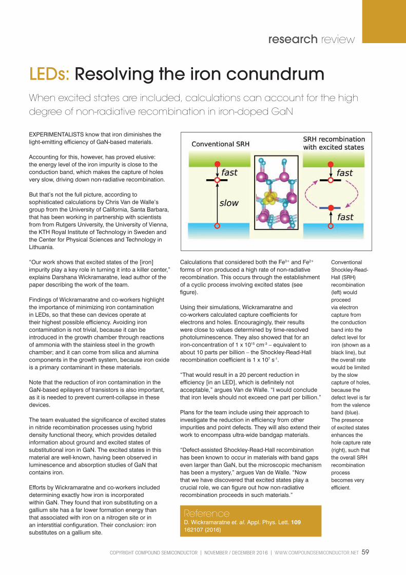
COPYRIGHT COMPOUND SEMICONDUCTOR l NOVEMBER / DECEMBER 2016 l WWW.COMPOUNDSEMICONDUCTOR.NET 59
research review
LEDs: Resolving the iron conundrumWhen excited states are included, calculations can account for the high degree of non-radiative recombination in iron-doped GaN
ReferenceD. Wickramaratne et. al. Appl. Phys. Lett. 109 162107 (2016)
EXPERIMENTALISTS know that iron diminishes the light-emitting efficiency of GaN-based materials.
Accounting for this, however, has proved elusive: the energy level of the iron impurity is close to the conduction band, which makes the capture of holes very slow, driving down non-radiative recombination.
But that’s not the full picture, according to sophisticated calculations by Chris Van de Walle’s group from the University of California, Santa Barbara, that has been working in partnership with scientists from from Rutgers University, the University of Vienna, the KTH Royal Institute of Technology in Sweden and the Center for Physical Sciences and Technology in Lithuania.
“Our work shows that excited states of the [iron] impurity play a key role in turning it into a killer center,” explains Darshana Wickramaratne, lead author of the paper describing the work of the team.
Findings of Wickramaratne and co-workers highlight the importance of minimizing iron contamination in LEDs, so that these can devices operate at their highest possible efficiency. Avoiding iron contamination is not trivial, because it can be introduced in the growth chamber through reactions of ammonia with the stainless steel in the growth chamber; and it can come from silica and alumina components in the growth system, because iron oxide is a primary contaminant in these materials.
Note that the reduction of iron contamination in the GaN-based epilayers of transistors is also important, as it is needed to prevent current-collapse in these devices.
The team evaluated the significance of excited states in nitride recombination processes using hybrid density functional theory, which provides detailed information about ground and excited states of substitutional iron in GaN. The excited states in this material are well-known, having been observed in luminescence and absorption studies of GaN that contains iron.
Efforts by Wickramaratne and co-workers included determining exactly how iron is incorporated within GaN. They found that iron substituting on a gallium site has a far lower formation energy than that associated with iron on a nitrogen site or in an interstitial configuration. Their conclusion: iron substitutes on a gallium site.
Calculations that considered both the Fe3+ and Fe2+ forms of iron produced a high rate of non-radiative recombination. This occurs through the establishment of a cyclic process involving excited states (see figure).
Using their simulations, Wickramaratne and co-workers calculated capture coefficients for electrons and holes. Encouragingly, their results were close to values determined by time-resolved photoluminescence. They also showed that for an iron-concentration of 1 x 1015 cm-3 – equivalent to about 10 parts per billion – the Shockley-Read-Hall recombination coefficient is 1 x 10⁷ s-1.
“That would result in a 20 percent reduction in efficiency [in an LED], which is definitely not acceptable,” argues Van de Walle. “I would conclude that iron levels should not exceed one part per billion.”
Plans for the team include using their approach to investigate the reduction in efficiency from other impurities and point defects. They will also extend their work to encompass ultra-wide bandgap materials.
“Defect-assisted Shockley-Read-Hall recombination has been known to occur in materials with band gaps even larger than GaN, but the microscopic mechanism has been a mystery,” argues Van de Walle. “Now that we have discovered that excited states play a crucial role, we can figure out how non-radiative recombination proceeds in such materials.”
Conventional Shockley-Read-Hall (SRH) recombination (left) would proceed via electron capture from the conduction band into the defect level for iron (shown as a black line), but the overall rate would be limited by the slow capture of holes, because the defect level is far from the valence band (blue). The presence of excited states enhances the hole capture rate (right), such that the overall SRH recombination process becomes very efficient.
Research Review v7MGRS.indd 59 28/11/2016 12:53

60 WWW.COMPOUNDSEMICONDUCTOR.NET l NOVEMBER / DECEMBER 2016 l COPYRIGHT COMPOUND SEMICONDUCTOR
research review
Etching the SiGe-on-insulator wafer (a) defines the pFET active region and an opening for the silicon seed (b). Sacrificial material is then added (c), before capping with an oxide and adding an opening to this layer (d). Sacrificial material is removed (e), before InGaAs grows from the seed (f) through the neck (g) to fill the cavity (h). The oxide cap is removed (i), before forming a nFET active region (j) and ultimately InGaAs nFETs and SiGe pFETs (k). A simplified process using a common high-κ/metal gate has been pursued by IBM Zurich (k’).
III-Vs: Combining logic and memoryTwo-dimensional integration forms invertors and SRAM
ReferenceL. Czornomaz et. al. VLSI (2016)
ENGINEERS at IBM Research Laboratory in Zurich, Switzerland, claim to have provided the first demonstration of CMOS invertors and dense SRAM arrays formed from InGaAs and SiGe devices on silicon.
These efforts differ from the vast majority of developmental work with InGaAs and SiGe transistors, which has focused solely on logic functions. Combining logic with memory is crucial, as in an advanced CPU, the SRAM cache can account for up to 80 percent of the total CPU area.
The primary motivation for building circuits with InGaAs and SiGe – alloys that have higher mobilities than silicon, and allow a reduction in the operating voltage of the circuit – is to improve the performance-power trade-off.
“We target to run our CMOS technology at an operating voltage of 0.5 volts, much lower than the typical 0.7-0.8 volts for advanced silicon technologies,” explains corresponding author Lukas Czornomaz.
If circuit designers could use this technology for servers, they could improve performance while maintaining today’s level of power consumption; and if they could employ it for making circuits for smartphones, they could slash power consumption while maintaining performance. Czornomaz and co-workers have produced their circuits with a two-dimensional integration scheme. This is the standard approach for making CMOS chips.
Their starting point, a 8 nm-thick Si0.75Ge0.25 channel on a 25 nm-thick buried oxide, is formed through germanium condensation on a silicon-on-insulator substrate. Dry etching forms the pFET active regions.
SiO2 cavities are then created, providing access to the silicon substrate. This occurs in the form of a crystalline seed, which is the starting point for the growth of InGaAs, which ideally expands to the desired shape and size.
Several other groups employ a different technology for forming III-Vs on silicon – they use long trenches that lead to many nucleation events. This creates multiple crystals, which generate a great deal of defects when they merge.
“By optimizing the growth conditions, the merging of crystals can be controlled to some extent,” argues
Czornomaz. “But it is clearly a limitation of the epitaxy-in-trenches approaches, like aspect ratio-trapping and replacement-fin [technologies].”
Device fabrication is completed with standard front-end-of-line processes with a gate-first scheme, to create modules with a raised-source/drain and high-κ/metal gate dielectric. These transistors then form the building blocks for inverters and memory cells with sizes ranging from 0.6 mm2 to 4.1 mm2.
Electrical characterisation of the transistors shows that SiGe pFETs with a 35 nm gate length do not suffer from short channel effects and produce a sub-threshold swing of 138 mV/dec. However, on-current is limited, due to the absence of a p-type, SiGe raised-source/drain.
The on-current for the In0.7Ga0.3As n-FET is much higher, but short-channel effects increase as the gate length is trimmed from 115 nm to 35 nm.
To reduce the short-channel effects, the team could move from planar devices to FinFETs, because this improves gate control over the channel as gate length shrinks below 20 nm; and they could switch from a gate-first process to a replacement-metal-gate process.
According to Czornomaz, the team’s next goals are to improve the performance of both types of device, and to scale down the technology to the required ground rules for the 7 nm node and beyond.
Research Review v7MGRS.indd 60 28/11/2016 12:53

The 2017 CS Industry Awards are NOW open for nominations
Make sure your company receives the recognition it deserves and enter the only compound semiconductor awards. Held in association with the CS International Conference 2017.
Closing date: 19 December 2016
www.csawards.net
7 MarchSheraton Brussels Airport Hotel, Belgium
CS Industry Awards Categories
£ Substrates and Materials
£ Metrology
£ High-volume Manufacturing
£ Device Design and Packaging
£ Innovation
62 WWW.COMPOUNDSEMICONDUCTOR.NET l NOVEMBER / DECEMBER 2016 l COPYRIGHT COMPOUND SEMICONDUCTOR
green pages directory
To promote your Products and Services contact: Shehzad Munshi T: +44 (0)1923 690 215E: [email protected]
Corporate Partners Green Pages 112016.indd 62 28/11/2016 13:03

COPYRIGHT COMPOUND SEMICONDUCTOR l NOVEMBER / DECEMBER 2016 l WWW.COMPOUNDSEMICONDUCTOR.NET 63
green pages directory
To promote your Products and Services contact: Shehzad Munshi T: +44 (0)1923 690 215E: [email protected]
Submit your Lab & Fab article
www.compoundsemiconductor.net
Research is the foundation for the growth of the compound semiconductor industry.
If you want to highlight the important breakthroughs that you make, submit your latest research stories to: [email protected] It is imperative that Compound Semiconductor remains a timely resource for this industry, so we are only interested in highlighting very recent work reported in academic papers.
Therefore, please only consider writing a short piece highlighting your work if you have a journal paper that has been accepted and about to appear in press, or a paper that has been published within the last month.
Corporate Partners Green Pages 112016.indd 63 28/11/2016 13:03

your!EPITAXIAL GROWTH!
partner!
Enabling advanced technologiesWorld leading technology
Complete materials range
MOCVD, MBE, CVD
Advanced semiconductor wafer products
Advanced R&D capabilities
Multiple, manufacturing sites (Europe, Asia, USA)
www.iqep.com
Untitled-1 1 02/07/2014 11:05Untitled-1 1 08/03/2016 10:23