Embed Size (px)
Citation preview

International Journal of Research Studies in Science, Engineering and Technology
Volume 2, Issue 9, September 2015, PP 1-15
ISSN 2349-4751 (Print) & ISSN 2349-476X (Online)
International Journal of Research Studies in Science, Engineering and Technology [IJRSSET] 1
Voltage Quality Improvement Using Improved DySC
Configuration
Mohammed Abdul Rahman Uzair1, Syed Misbahuddin Moeez
2,
Syed Saifuddin Zeeshan3, Syed Husoor Ullah Quadri
4
1Research Scholar, EEE, GITAM University- Hyderabad, India
2,3,4Under Graduate Student, Nawab Shah Alam Khan College of Engg & Tech,
Malakpet- Hyderabad, India [email protected],
Abstract: Power Quality (PQ) problems have obtained increasing attentions as they can affect lots of sensitive
end-users. Studies indicate that voltage sags, transients and momentary interruptions constitute 92% of all the
PQ problems occurring in the distribution power system. Typical sag can be a drop between 10% and 90% of
the rated rms voltage and has the duration time of 0.5 cycles to 1 min. According to the data presented, majority
of the sags recorded are of depth no less than 50%, but deeper sags with long duration time obviously cannot be
ignored as they are more intolerable than shallow and short-duration sags to the sensitive electrical consumers.
The most studied voltage regulator topologies can be generally categorized into two groups: the inverter-based
regulator and direct AC–AC converters. Series-connected Devices (SD) are voltage-source inverter-based
regulators and an SD compensate for voltage sags by injecting a missing voltage in series with the grid.
In the proposed paper, a new topology of series-connected compensator is presented to mitigate long duration
deep sags, and the compensation ability is highly improved with a unique shunt converter structure acting as a
parasitic boost circuit that has been theoretically analyzed. Further, the proposed active voltage quality
regulator is a cost effective solution for long duration sags that are lower than 50% of the nominal voltage as it
is transformer-less compared to the traditional dynamic voltage restorer. High operation efficiency is ensured
by applying the DC-link voltage adaptive control method. Analysis, along with simulation results, is presented
to verify the feasibility and effectiveness of the proposed topology.
Keywords: Power quality, voltage sags, Series-connected devices, DC-link, MATLAB.
1. INTRODUCTION
Many power devices have been proposed to mitigate voltage sags for sensitive loads. The used
topologies are: the AC inverter-based regulator and direct AC-AC converters. Series-connected
Devices (SD) are voltage-source inverter-based regulators and they compensate voltage sags by
injecting the missing voltage in series with the grid. The key features related to the evaluation of
certain SD topologies are cost, complexity and compensation ability. Dynamic Voltage Restorer
(DVR) is a commonly used SD. Four typical DVR system topologies are investigated and
experimentally compared. The evaluation shows that DVR with no storage and load-connected shunt
converter ranks the highest as it can compensate long duration deep sags at a relatively low
complexity and cost.
DySC is changed according to the structural differences between the DVR with load-connected shunt
converter and the one with supply-connected shunt converter. As a result, the shunt converter together
with the series converter forms a boost charging circuit and the DC-link voltage will be charged to
exceed the peak value of supply voltage. Thus obtained novel topology is called the transformer-less
active voltage quality regulator with the parasitic boost circuit (PB-AVQR), and it is capable of
mitigating long-duration deep voltage sags without increasing the cost, volume and complexity
compared with the traditional DySC topology. The DC-link voltage adaptive control method proposed
and is also applied in the PB-AVQR to improve its efficiency.
This paper starts with introducing the operating mode and working principles of the proposed
configuration. Then, the parasitic boost circuit model is provided followed by the theoretical analysis
to calculate its DC-link voltage. At last, the simulation results using MATLAB and experimental
results on a 220V- 2kW prototype are given to verify the feasibility and effectiveness of the PB-
AVQR topology.
Voltage Quality Improvement Using Improved DySC Configuration
International Journal of Research Studies in Science, Engineering and Technology [IJRSSET] 2
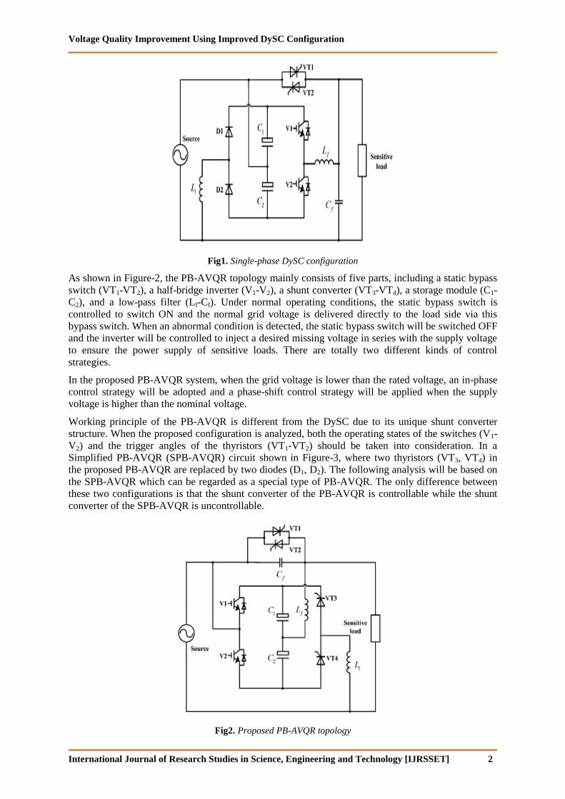
Fig1. Single-phase DySC configuration
As shown in Figure-2, the PB-AVQR topology mainly consists of five parts, including a static bypass
switch (VT1-VT2), a half-bridge inverter (V1-V2), a shunt converter (VT3-VT4), a storage module (C1-
C2), and a low-pass filter (Lf-Cf). Under normal operating conditions, the static bypass switch is
controlled to switch ON and the normal grid voltage is delivered directly to the load side via this
bypass switch. When an abnormal condition is detected, the static bypass switch will be switched OFF
and the inverter will be controlled to inject a desired missing voltage in series with the supply voltage
to ensure the power supply of sensitive loads. There are totally two different kinds of control
strategies.
In the proposed PB-AVQR system, when the grid voltage is lower than the rated voltage, an in-phase
control strategy will be adopted and a phase-shift control strategy will be applied when the supply
voltage is higher than the nominal voltage.
Working principle of the PB-AVQR is different from the DySC due to its unique shunt converter
structure. When the proposed configuration is analyzed, both the operating states of the switches (V1-
V2) and the trigger angles of the thyristors (VT1-VT2) should be taken into consideration. In a
Simplified PB-AVQR (SPB-AVQR) circuit shown in Figure-3, where two thyristors (VT3, VT4) in
the proposed PB-AVQR are replaced by two diodes (D1, D2). The following analysis will be based on
the SPB-AVQR which can be regarded as a special type of PB-AVQR. The only difference between
these two configurations is that the shunt converter of the PB-AVQR is controllable while the shunt
converter of the SPB-AVQR is uncontrollable.
Fig2. Proposed PB-AVQR topology

Mohammed Abdul Rahman Uzair et al.
International Journal of Research Studies in Science, Engineering and Technology [IJRSSET] 3
Fig3. SPB-AVQR topology
That is to say, the DC-link voltage of the SPBAVQR represents the upper limit of the DC-link voltage
in the PB-AVQR structure.
Both the compensation process and charging process can be explained based on these operating
conditions. In Figures-4 & 5, the solid line means that there is current flowing through and arrows
depict directions.
Operating conditions during the positive half-cycle are illustrated in Figure-4. When V2 is switched
ON, as shown in Figure-4(a), the grid charges the inductor L1 via the diode D2 and the capacitor C2
discharges to maintain the load voltage. When V2 is switched OFF, as shown in Figure-4(b), the
energy stored in the inductor during previous period is released to DC-link capacitors C1 and C2
through VD1 which is the anti parallel diode of V1. Operating conditions during the negative half-
cycle are given in Figure-5. When V1 is switched ON, as shown in Figure-5(a), the inductor L1 is
charged via the diode D1, and the load is compensated by the capacitor C1. When V1 is switched OFF,
as shown in Figure-5(b), the energy stored in L1 is released through VD2, which is the anti parallel
diode of V2, to capacitors C1 and C2.
So, in each half-cycle of the grid, one capacitor of the DC-link discharges to provide the energy
needed for the compensation, and this energy is actually obtained from the supply source via the
charging process described earlier.
Apparently, the charging circuit of the proposed configuration works exactly like a boost circuit and
the DC-link voltage in this situation is controlled by the duty ratio of the two switches.
So, the compensation ability of the SPB-AVQR is theoretically unlimited as long as the grid is strong
enough to provide the needed power. However, as the boost circuit is parasitic on the series inverter,
and the two switches are actually controlled according to the missing voltage, there still exist some
restrictions. The relationships between the DC-link voltage and other system parameters will be
discussed in the next section. In Figures-4 and 5, two endpoints of the inverter are marked as a and b.
Parts of the waveforms obtained at the inverter side and load side under four operating conditions are
schematically shown in Figure-4, where VaN represents the voltage between a and N. As shown in
Figure-5, when V1/V2 is switched ON/OFF, the DC-link voltage will be added/subtracted to the
supply voltage to get a switching pulse voltage Ua and the switching harmonics of UaN will be filtered
by Lf and Cf to get a smooth load voltage. The load voltage will hence be maintained at its rated value
if the inverter is properly controlled according to the required missing voltage during sags.

Voltage Quality Improvement Using Improved DySC Configuration
International Journal of Research Studies in Science, Engineering and Technology [IJRSSET] 4
Fig4. Operating conditions during positive half-cycle (a) V2 switched ON (b) V2 switched OFF
Fig5. Operating conditions during negative half-cycle (a) V1 switched ON (b) V1 switched OFF
Mohammed Abdul Rahman Uzair et al.
International Journal of Research Studies in Science, Engineering and Technology [IJRSSET] 5
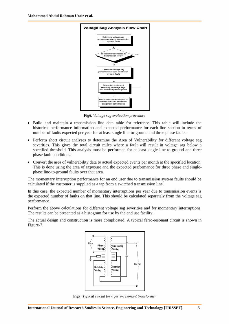
Fig6. Voltage sag evaluation procedure
Build and maintain a transmission line data table for reference. This table will include the
historical performance information and expected performance for each line section in terms of
number of faults expected per year for at least single line-to-ground and three phase faults.
Perform short circuit analyses to determine the Area of Vulnerability for different voltage sag
severities. This gives the total circuit miles where a fault will result in voltage sag below a
specified threshold. This analysis must be performed for at least single line-to-ground and three
phase fault conditions.
Convert the area of vulnerability data to actual expected events per month at the specified location.
This is done using the area of exposure and the expected performance for three phase and single-
phase line-to-ground faults over that area.
The momentary interruption performance for an end user due to transmission system faults should be
calculated if the customer is supplied as a tap from a switched transmission line.
In this case, the expected number of momentary interruptions per year due to transmission events is
the expected number of faults on that line. This should be calculated separately from the voltage sag
performance.
Perform the above calculations for different voltage sag severities and for momentary interruptions.
The results can be presented as a histogram for use by the end use facility.
The actual design and construction is more complicated. A typical ferro-resonant circuit is shown in
Figure-7.
Fig7. Typical circuit for a ferro-resonant transformer
Voltage Quality Improvement Using Improved DySC Configuration
International Journal of Research Studies in Science, Engineering and Technology [IJRSSET] 6
Ferro-resonant transformers output over 90% normal voltage as long as the input voltage is above a
minimum value, at which the output collapses to zero voltage. Voltage support during voltage sags
can be very good if the CVT is oversized for the load.
2. WORKING OF PROPOSED CIRCUIT
CVTs will handle the majority of voltage sag conditions. If voltage sags which are too severe for
CVTs or if the loads are too large for protection with CVTs, a specific energy storage technology will
have to be used for ride-through support. Protection for extremely critical loads, such as life safety
systems and critical data processing equipment, should include UPS systems or the equivalent for
complete backup capability. New energy storage technologies that can provide short duration backup
for large portions of a facility are now becoming available. These include superconducting magnetic
energy storage, flywheels and advanced battery systems. DC-link voltage is a key parameter to
evaluate the compensation ability about a series compensation device since it decides the maximum
value of the injected compensation voltage.
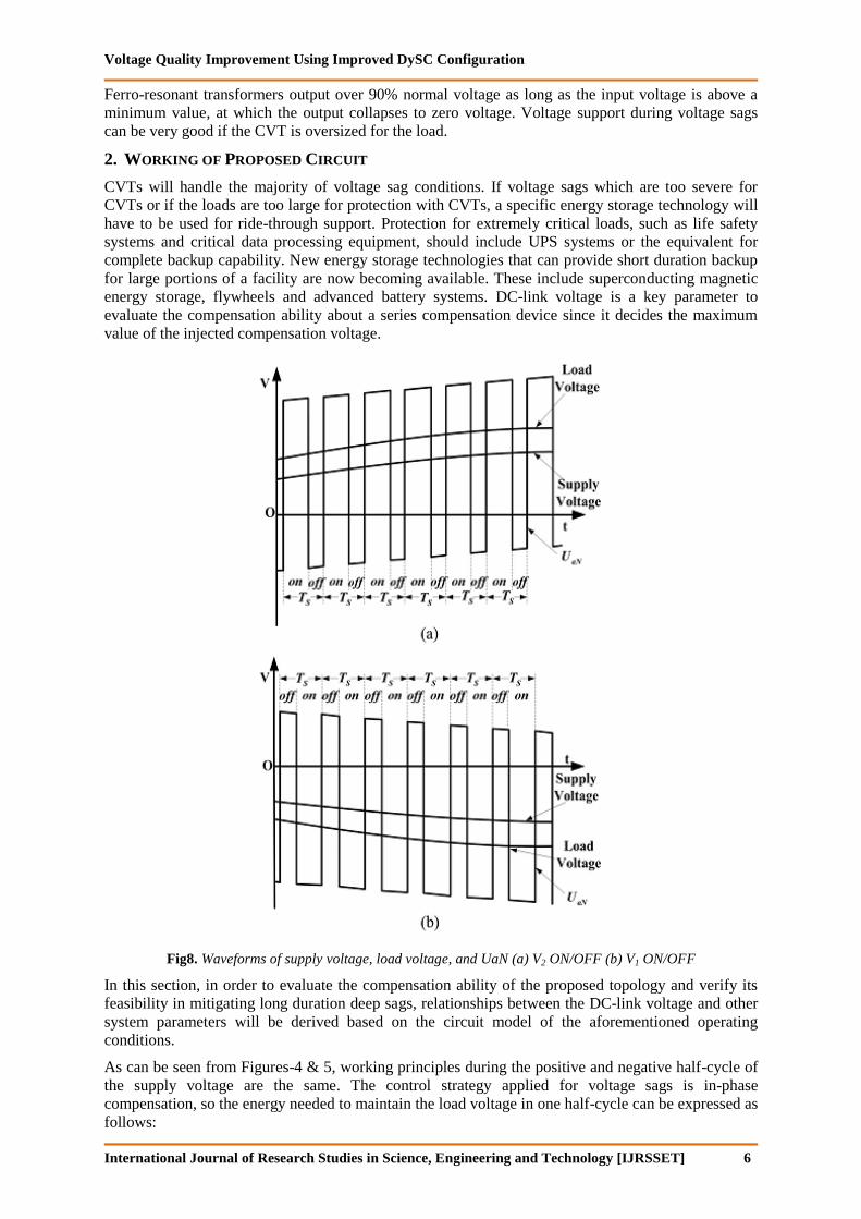
Fig8. Waveforms of supply voltage, load voltage, and UaN (a) V2 ON/OFF (b) V1 ON/OFF
In this section, in order to evaluate the compensation ability of the proposed topology and verify its
feasibility in mitigating long duration deep sags, relationships between the DC-link voltage and other
system parameters will be derived based on the circuit model of the aforementioned operating
conditions.
As can be seen from Figures-4 & 5, working principles during the positive and negative half-cycle of
the supply voltage are the same. The control strategy applied for voltage sags is in-phase
compensation, so the energy needed to maintain the load voltage in one half-cycle can be expressed as
follows:

Mohammed Abdul Rahman Uzair et al.
International Journal of Research Studies in Science, Engineering and Technology [IJRSSET] 7
E0 = (T0 ∆V / 2Vref) P0 (1)
Where T0 is the grid voltage period time, Vref is the rated rms value of the load voltage, P0 is the rated
load power, and ΔV is the rms value of the missing voltage. In steady-state compensation, the energy
needed for the compensation should completely be provided by the residential grid which is also the
charging energy through the parasitic boost circuit in this case. The charging energy provided during
T0/2 referred to as E1 equals to E0. E0 can be easily obtained according to (1), but the calculation of E1
involves with the operating conditions shown in Figure-4. The simplified circuit model of Figure-3 is
illustrated in Figure-9, where compensation loop including the filter and the load is ignored and only
the charging circuit is considered.
Fig9. Simplified circuit model (a)V2 turned ON (b)V2 turned OFF
In Figure-9, VS is the rms value of the supply voltage. Two state equations can be obtained based on
Figure-9 and written as follows:
L1dIon/dt = √2 Vs sin(ωt)
L1dIoff/dt = √2 Vs sin(ωt) - Vdc1 - Vdc2 (2)
The analysis will be significantly simplified if some realistic approximations are carried out.
Then (2) can be discredited into (3) based on two following assumptions: C1 and C2 are well designed
so that Vdc1 and Vdc2 can be regarded equal without considering their ripple voltages; the switching
frequency is much higher than the line frequency that the supply voltage in the nth switching cycle
can be treated as a constant value.
L1ΔIonn = √2 Vs sin(ωnTs)tonn
L1ΔIoffn = [√2 Vs sin(ωnTs) – 2Vdc]toffn (3)
Where tON and tOFF n are, respectively, the turn-ON and turn-OFF time of V2 in the nth switching cycle,
Ts is the switching period, Vdc is the steady-state DC-link voltage, and ΔION n or ΔIOFF n represents the
variation amount in charging current during ton or toff n. As the analysis is within the positive half-cycle
of the grid, there exists a constraint: n≤T0/2Ts. Apparently, ton and toff n here are actually the
inverter‟s duty cycle and they can be expressed as (4) when two-level symmetric regular-sampled
PWM method is adopted .

Voltage Quality Improvement Using Improved DySC Configuration
International Journal of Research Studies in Science, Engineering and Technology [IJRSSET] 8
tonn = Ts/2 [1 + √2 ΔVsin(ωnTs)/Vdc]
toffn = Ts/2 [1 - √2 ΔVsin(ωnTs)/Vdc] (4)
The recursion formula of the charging current at the end of the nth switching cycle can be obtained by
combining (3) and (4)
Ioffn = Ioff(n-1) + Ts/L1 [√2 Vref sin(ωnTs) – Vdc] (5)
Where IOFFn represents charging current instantaneous value at the end of the nth switching cycle and
ΔION n can be derived at the same time
ΔIonn = √2 Ts Vs sin(ωnTs)/2L1 [1 + √2 V sin(ωnTs)/Vdc] (6)
The energy stored in an inductor is related to the current that flows through it, so the charging energy
provided by the grid via the parasitic boost circuit in the nth switching cycle can be expressed and
then rearranged as follows:
Einn = 1/2 L1 Δ I2onn + L1 Ioff(n-1) Δ Ionn (7)
IOFF (n−1) in (7) can be superimposed according to the recursion formula shown in (5). Before the
expression is given, there are some features about the charging current should be clarified:
The value of the charging current cannot be lower than zero as the current flowing through a diode
is unidirectional.
The value of the charging current can either be zero or nonzero and its value always decreases after
increasing in one half-cycle of the sinusoidal grid voltage. Then, the nonzero terms of the charging
current can be derived as follows:
Ioff(n-1) = n-1
Σk=n0 Ts/L1 [√2 Vref sin(ωkTs) – Vdc] (8)
Where n0 is the initial superposition instant and Ioff n is always equal to zero when n is smaller than
n0. So, n0 can be calculated according to (5) and expressed as follows:
n0 = ceil [T0 arcsin(Vdc/Vref) / 2πTs] (9)
Where „ceil(•)‟ represents the rounded up function and the arcsine function There ranges from 0 to
π/2. Furthermore, when the charging current calculated by (8) decreases to the value no more than
zero , n will reach its upper limit denoted by ne. Substituting the above values, the energy provided by
the supply in the nth switching cycle can be written as follows:
Einn=(Ts2Vs
2A
2/4L1)(1+√2BA)
2+(√2Ts
2VsA/2L1Vdc)(Vdc+√2∆VA)
n-1Σk=n0(√2VrefC-Vdc) (10)
where,
A = sinωnTs
B = ΔV/Vdc
C = sinωkTs
E1 now can be obtained if (10) is added with n ranging from 1to T0/2Ts. So, the overall energy balance
equation can be written as follows:
E1 = T2
s V2
s/4L1 [(T0/2Ts
Σn=1 A2) + ( 2√2 B
T0/2TsΣn=1 A
3) + (2B
2 T0/2Ts
Σn=1 A4)] (11)
The charging current peak value Imax is considered to arise at the switching cycle after the value of (8)
reaches its upper limit. So Imax is expressed as follows:
Imax = √2 Ts Vs sin(ωnmaxTs) [1 + √2 B sin(ωnmaxTs)]/2L1 + nmax
Σn=n0 Ts (√2 Vref C – Vdc)/L1 (12)
Where nmax is the switching cycle when Ioff reaches its maximum value and nmax can be written as
follows:
nmax = ceil [T0 (π – arcsin(Vdc/Vref))/2πTs] (13)
So far, the main features of the SPB-AVQR topology can be described by (11) and (12). As shown in
(11), the DC-link voltage is not only related to the supply voltage, but also associated with the
charging inductance, load active power, and switching frequency.

Mohammed Abdul Rahman Uzair et al.
International Journal of Research Studies in Science, Engineering and Technology [IJRSSET] 9
However, the DC-link voltage cannot be obtained directly from (11) as n0 and ne cannot be computed
with unknown DC-link voltage. So, an iterative algorithm is applied to estimate the DC-link voltage,
where Ts, VS, T0, Vref, L1 and P0 are all treated as constants. A flow chart of the adopted calculating
method is illustrated in Figure-8, whereVdc0 is the initial value for Vdc and ΔVdc is the iterative step.
The algorithm is terminated if the error between E0 and E1 is smaller than the error tolerance ε.
Moreover, the charging current can be calculated by (12) and (13) as long as Vdc is obtained.
Figure-11 shows the relationships between the steady-state dc link voltage and the supply voltage
with different inductance values obtained according to (11). Other system parameters are listed as
follows:P0=2kW,Ts=(1/15000)s,T0=0.02s,Vref=220V.
The black solid line in Figure-11 is the Vdc−VS curve of the DySC topology. As can be seen in Figure-
11, the steady-state DC link voltage of the SPB-AVQR under different supply voltage is much higher
than that of the DySC topology and it decreases slightly with the falling of the supply. Additionally,
when the supply voltage is lower than 50% of its rated value, the dc-link voltage of the SPB-AVQR is
still maintained high enough for the compensation while that of the DySC is too low to mitigating the
deep sag. Figure-11 also indicates that the dc-link voltage of the SPB-AVQR becomes higher with a
lower inductance under the same circumstances. Figure-12 gives the Imax−VS curve under the same
condition. It presents that the steady-state charging current peak value increases with the decreasing of
the supply voltage and it can be suppressed by increasing the charging inductance.
Although conclusions drawn from the theoretical analysis for the SPB-AVQR can also be applied to
the proposed PB-AVQR topology, there still exist some differences in their dc-link voltages. When
the proposed PB-AVQR is discussed, the trigger pulse angle α for VT3 and VT4 should also be taken
into consideration. In the PB-AVQR circuit, the charging process begins after the VT3 or VT4 is
triggered, so the initial superposition instant n0 in (11) is now determined by α denoted byn1 and the
energy balance equation is written as follows:
(T2s V
2s / 4L1) (
ncΣn=n1 A
2 + 2√2 B
ncΣn=n1 A
3 + 2B
2
ncΣn=n1 A
4) + (T
2s V
2s/2L1)
ncΣn=n1 [(A+√2 BA
2)
n-
1Σn=n1 (√2 Vref C-Vdc)] = [T0ΔV/2Vref] P0 (14)
Fig10. Flow chart for calculating Vdc

Voltage Quality Improvement Using Improved DySC Configuration
International Journal of Research Studies in Science, Engineering and Technology [IJRSSET] 10
Fig11. Vdc − VS curve of the SPB-AVQR with different inductances.
Fig12. Imax−VS curve of the SPB-AVQR with different inductances
Fig13. Vdc−VS curve of the PB-AVQR with different trigger angles

Mohammed Abdul Rahman Uzair et al.
International Journal of Research Studies in Science, Engineering and Technology [IJRSSET] 11
Here, n is still determined by (8) as aforementioned and n1 can be derived as follows:
n1 = ceil (αT0/ 2πTs) (15)
Furthermore, the thyristors are triggered only once in each half-cycle and the current through them
should be higher than the holding current to maintain the triggered state. So, α is required to meet the
constraint expressed as follows:
√2 Vref sinα > Vdc (16)
The charging current peak value of the PB-AVQR can still be described by (12) as long as n0 is
substituted with n1.
As can be seen from (14) and (15), the trigger pulse of the PB-AVQR will certainly affect its DC-link
voltage and charging current. Figure-13 shows the Vdc−VS curve under the influence of α according to
(14). The charging inductor in Figure-13 is set to 2mH and other parameters remain the same as those
in Figure-11.
Figure-13 demonstrates the steady-state DC-link voltage gets higher with a smaller trigger angle as
the charging time becomes longer.
Fig14. Imax−VS curve of the PB-AVQR with different trigger angles
It also indicates that the PB-AVQR is capable of mitigating deep sags with a proper trigger pulse.
Figure -14 presents how α affects the Imax−VS curve under the same condition. As shown in Figure-14,
the charging current peak value can be reduced by decreasing α with the s5me supply voltage.
3. SOFTWARE REQUIRED
The software used for simulation of the proposed model is MATLAB.
The Software version is R2009b.
In order to show the validity of the proposed PB-AVQR, simulation and experimental results are
presented in this section. The simulation results are based on the MATLAB software and the
experimental results are based on a 2kW single-phase prototype. The control method applied for the
inverter is proposed and the control method for the thyristors is demonstrated.
System parameters:
There are mainly four parameters need to be designed, namely the dc-link capacitor C1/C2, the filter
inductor Lf, the filter capacitor Cf, and the charging inductor L1. During the steady-state
compensation, one capacitor discharges at the switched-on position and two capacitors are both
charged at the switched-off position in each switching cycle. Furthermore, C1 and C2 discharge,
respectively, in the negative and positive half-cycle of the supply. So, if the two capacitors are treated
equally during the charging process, the energy-balance equation that required for the capacitors can
be written as

Voltage Quality Improvement Using Improved DySC Configuration
International Journal of Research Studies in Science, Engineering and Technology [IJRSSET] 12
(T0ΔV/4Vref) P0 = 1/2[C1(2)V2dc] – 1/2[C1(2)(Vdc – νdc)
2] (17)
where Vdc is the fluctuation voltage of Vdc. In the theoretical analysis, the DC-link voltage is assumed
to be a constant, Vdc/Vdc here is limited within 5% at the voltage drop of 50% to minimize the overall
dc-link voltage ripple. In this way, the estimated minimum value of C1/C2 can be calculated according
to (17) with Vdc substituted by the dc-link set value Vdc-set. How to set the DC-link value is
introduced in and it is given as,
Vdc-set = 1.2 × √2(Vref – Vs) + 40 Vs < Vref
1.5 × √2(V2
s – V2ref) + 40 Vs > Vref (18)
Table1. Key Parameters according to design principles
Description Parameters Real Value
Nominal Voltage Vref 220 V
Line Frequency f0 50 Hz
Switching Frequency fs 15 kHz
DC-Link Capacitor C1 / C2 4700 µF
Filter Inductor Lf 1.5 mH
Filter Capacitor Cf 20 µF
Charging Inductor L1 2 mH
As shown in Figures-11 to 14, a higher DC-link voltage will be obtained with a smaller L1, but the
peak value of the charging current will get larger at the same time. So, charging inductance L1 is
designed as a result of the compromise between the compensation ability and the charging current
peak value. The main function of the output LC filter in the proposed structure is to eliminate the
harmonic components of the injected compensation voltage. The value of Lf and Cf are designed
according to its natural frequency and several other criterions which are given as follows:
1/2π√LfCf = χ ƒ8
Lf < νL/ ω0 ILmax
Cf < Iripple (χ2 + 1)/8Vdcƒ8 (19)
Where, fs is the switching frequency, vL is the voltage drop across the inductor Lf at ILmax, ILmax is
the maximum value of the load current, Iripple is the maximum ripple current of the filter and χ is the
coefficient between the switching frequency and the filter‟s natural frequency. Generally, χ ranges
from 0.05 to 0.2.The PB-AVQR system‟s key parameters are listed in Table-1 according to the design
principles mentioned earlier.
4. SIMULATION RESULTS
Fig16. Simulation result of the DySC

Mohammed Abdul Rahman Uzair et al.
International Journal of Research Studies in Science, Engineering and Technology [IJRSSET] 13
As shown in Figure-16, when the supply voltage is 180V, the DySC can effectively compensate for
the voltage sag. However, when the supply voltage drops to 100V, the load voltage becomes not
sinusoidal as the maximum injected compensation voltage is limited by the low steady-state DC-link
voltage. Figure-16 also indicates that the DySC can only mitigate deep sags for a few line cycles
depending on the energy stored in DC-link capacitors as its steady-state DC-link voltage is always
lower than the peak value of the supply voltage.
Fig17. Simulation result of the PB-AVQR
The simulation results of the proposed PB-AVQR topology under the same condition is shown in
Figure-17. In Figure-17, when supply voltage changes, the dc-link voltage precisely tracks Vdc-set
according to (18) and it also remains enough high for the compensation even with a 100V supply
voltage. Figure-17 also indicates that the transient response here is not very good, but this can be
improved by increasing the set value for dc-link voltage. The active power of the supply during the
steady-state compensation is 2kW, and it is the same as the load power which means that the load
voltage is effectively ensured. The reactive power during the steady-state compensation is about
1.1KVAR with 180V supply and is about 1.4KVAR with 100 V supply.
Fig18. Trigger signals under different supply voltage values (a) 180V supply (b) 100V supply

Voltage Quality Improvement Using Improved DySC Configuration
International Journal of Research Studies in Science, Engineering and Technology [IJRSSET] 14
The reactive power of the proposed PB-AVQR is higher than that of the DySC due to the dc-link
voltage adaptive control method. Additionally, the instantaneous value of the active and reactive
power can be suppressed by properly designing Vdc-set and the charging time of the capacitors.
Figure-18 shows trigger pulses for thyristors under different grid voltage. The supply voltage is 180V
in Figure-18(a) and is 100V in Figure-18(b). As shown in Figure-18, the trigger angle becomes
smaller to ensure the compensation energy needed when the grid voltage decreases.
5. CONCLUSION
This paper has presented a novel transformer-less active voltage quality regulator with parasitic boost
circuit to mitigate long duration deep voltage sags. The proposed PB-AVQR topology is derived from
the DySC circuit and the compensation performance is highly improved without increasing the cost,
weight, volume, and complexity. It is a relatively cost-effective solution for deep sags with long
duration time compared with the traditional DVR topology with load-side-connected shunt converter
as a series transformer is no longer needed. The working principle and circuit equations are given
through theoretical analysis. Simulation and experimental results are presented to verify the feasibility
and effectiveness of the proposed topology in the compensation for long duration deep voltage sags
that are lower than half of its rated value. The operating efficiency of the proposed PB-AVQR system
also remains at a relatively high level as the DC-link voltage adaptive control method is adopted. In a
conclusion, the proposed PB-AVQR topology in this paper provides a novel solution for long
duration deep voltage sags with great reliability and compensation performance.
REFERENCES
[1] A. Sannino, M. G. Miller, and M. H. J. Bollen, “Overview of voltage sag mitigation,” in Proc.
IEEE Power Eng. Soc. Winter Meet., 2000, vol. 4, pp. 2872–2878.
[2] S. M. Hietpas and M. Naden, “Automatic voltage regulator using an AC voltage-voltage
converter,” IEEE Trans. Ind. Appl., vol. 36, no. 1, pp. 33– 38, Jan./Feb. 2000.
[3] J. G. Nielsen and F. Blaabjerg, “A detailed comparison of system topolo-gies for dynamic voltage
restorers,” IEEE Trans. Ind. Appl., vol. 41, no. 5, pp.1272–1280, Sep./Oct. 2005.
[4] A. K. Sadigh, E. Babaei, S. H. Hosseini, and M. Farasat, “Dynamic voltage restorer based on
stacked multicell converter,” in Proc. IEEE Symp. Ind. Electron. Appl., 2009, pp. 419–424.
[5] Anil Mudireddy, Sathish Bandaru “Voltage quality regulator using boost converter,” ISSN:2248-
9278/Aug-Sep14/Vol-13/Issue-1/pg.1030-1039.

Mohammed Abdul Rahman Uzair et al.
International Journal of Research Studies in Science, Engineering and Technology [IJRSSET] 15
AUTHORS’ BIOGRAPHY
Mohammed Abdul Rahman Uzair was born at Nalgonda, a district headquarter
nearly 100kms from Hyderabad, India. He completed his BTech in Electrical and
Electronics Engineering, from JNTU Hyderabad in the year 2003. He completed
his MTech in Electrical Power Engineering, from JNTU Hyderabad in the year
2012. Currently, he is pursuing PhD from GITAM University, Hyderabad campus
on the topic „Failure Analysis of Power Transformers‟. He is working as Associate
Professor in the Department of EEE at Nawab Shah Alam Khan College of Engg
& Tech, Hyderabad. His fields of interest are Power Systems and Power
Electronics. He has published five papers so far- one in a National Journal (2011), three in
International Journals (2013,2015,2015) apart from an IEEE paper (2015).
Syed Misbahuddin Moeez was born at Hyderabad, India. He completed his
BTech in Electrical and Electronics Engineering, from JNTU Hyderabad in the
year 2015. His fields of interest are Power Systems and Power Electronics.
Syed Saifuddin Zeeshan was born at Hyderabad, India. He completed his BTech
in Electrical and Electronics Engineering, from JNTU Hyderabad in the year 2015.
His fields of interest are Power Systems and Power Electronics.
Syed Husoorullah Quadri was born at Hyderabad, India. He completed his
BTech in Electrical and Electronics Engineering, from JNTU Hyderabad in the
year 2015. His fields of interest are Power Systems, Power Electronics Control
Systems, Electrical Machines, High Voltage Engineering and Electrical Circuits.