Embed Size (px)
Citation preview

EECS 270C / Spring 2014 Prof. M. Green / U.C. Irvine 1
Voltage-Controlled Oscillator (VCO)
VC
fosc
fmin
fmax
slope = Kvco
Desirable characteristics: • Monotonic fosc vs. VC characteristic
with adequate frequency range • Well-defined Kvco
€
φout =Kvco
s + KPDKvcoF (s) / N⋅φVC
^ ^
Noise coupling from VC into PLL output is directly proportional to Kvco.
€
φin
€
φout
€
φVC
€
KPD
€
F (s)
€
Kvco
s
^
€
÷N
€
VC
€
VD +

EECS 270C / Spring 2014 Prof. M. Green / U.C. Irvine 2
Oscillator Design
€
A(s)
€
f
€
Vin ⇒ 0
€
Vout
€
Vout
Vin
≡HCL (s) =A(s)
1+ f ⋅A(s)
loop gain
Barkhausen’s Criterion:
If a negative-feedback loop satisfies:
€
f ⋅ A jωo( ) ≥1
∠A jωo( ) = −180!
then the circuit will oscillate at frequency ω0.

EECS 270C / Spring 2014 Prof. M. Green / U.C. Irvine 3
Inverters with Feedback (1)
V1 V2
V1
V2 1 inverter
feedback
V1
V2
2 inverters
feedback
1 stable equilibrium point
3 equilibrium points: 2 stable, 1 unstable (latch)
1 inverter:
V1 V2
2 inverters:

EECS 270C / Spring 2014 Prof. M. Green / U.C. Irvine 4
Inverters with Feedback (2)
3 inverters forming an oscillator:
1 unstable equilibrium point due to phase shift from 3 capacitors
V1 V2
V1
V2
Let each inverter have transfer function
€
Hinv ( jω) =A0
1+ jω p
€
Hloop ( jω) = Hinv ( jω)[ ]3
=A
0
3
1+ jω p( )3
Loop gain:
Applying Barkhausen’s criterion:
€
∠Hloop ( jω) = −3 tan−1 ωp
%
& '
(
) * = −180! ⇒ ωo = 3⋅ p
€
Hloop ( jωo ) =A
0
3
1+ 3[ ]3
2> 1 ⇒ A0 > 2

EECS 270C / Spring 2014 Prof. M. Green / U.C. Irvine 5
Ring Oscillator Operation
VA VB VC
tp tp tp
VA
VB
VC
VA
tp
tp
tp
€
12
Tosc
12Tosc = 3tp
⇒Tosc = 6tp

EECS 270C / Spring 2014 Prof. M. Green / U.C. Irvine 6
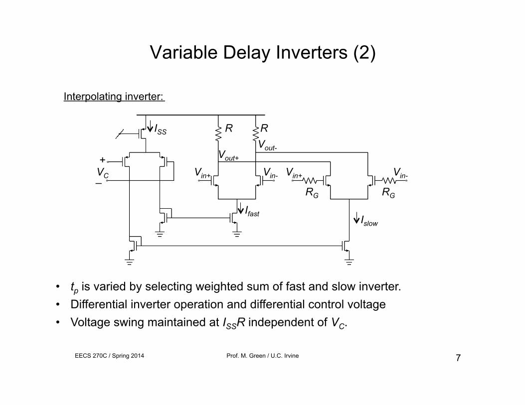
Variable Delay Inverters (1)
VC
Vin Vout
Current-starved inverter: Inverter with variable load capacitance:
Vin Vout
VC
EECS 270C / Spring 2014 Prof. M. Green / U.C. Irvine 7
Variable Delay Inverters (2)
R R
Vin+ Vin- Vin+ Vin-
Vout- Vout+
Ifast Islow
RG RG
ISS
VC +
_
Interpolating inverter:
• tp is varied by selecting weighted sum of fast and slow inverter. • Differential inverter operation and differential control voltage • Voltage swing maintained at ISSR independent of VC.

VA
VB
VC
VD
tp
tp
tp
€
12
Tosc
tp
VA
EECS 270C / Spring 2014 Prof. M. Green / U.C. Irvine 8
Differential Ring Oscillator
additional inversion (zero-delay)
VA + −
Use of 4 inverters makes quadrature signals available.
VB + −
VC + −
VD + −
VA − +
12Tosc = 4tp
⇒Tosc = 8tp

EECS 270C / Spring 2014 Prof. M. Green / U.C. Irvine 9
Resonance in Oscillation Loop
€
Hr (s)
€
Hr (s)
ω ωr
€
Hr ( jω)
€
∠Hr ( jω)
ω ωr
€
+π2
€
−π2
1
At dc: Since Hr(0) < 1, latch-up does not occur.
At resonance:
€
Hr ( jωr ) > 1
∠Hr ( jωr ) = 0
€
⇒ ωo =ω r

EECS 270C / Spring 2014 Prof. M. Green / U.C. Irvine 10
LC VCO
Vin Vout
Vin Vout
€
Hr (s)
C L
€
ωr =1LC
€
⇒
realizes negative resistance
2L
C C
€
Hr (s)
€
Hr (s)
€
⇒

EECS 270C / Spring 2014 Prof. M. Green / U.C. Irvine 11
A. Reverse-biased p-n junction
+ – VR
VR
Cj
B. MOSFET accumulation capacitance
+
–
VBG
varactor = variable reactance
Variable Capacitance
VBG
Cg
accumulation region
inversion region
p-channel
n diffusion in n-well
EECS 270C / Spring 2014 Prof. M. Green / U.C. Irvine 12
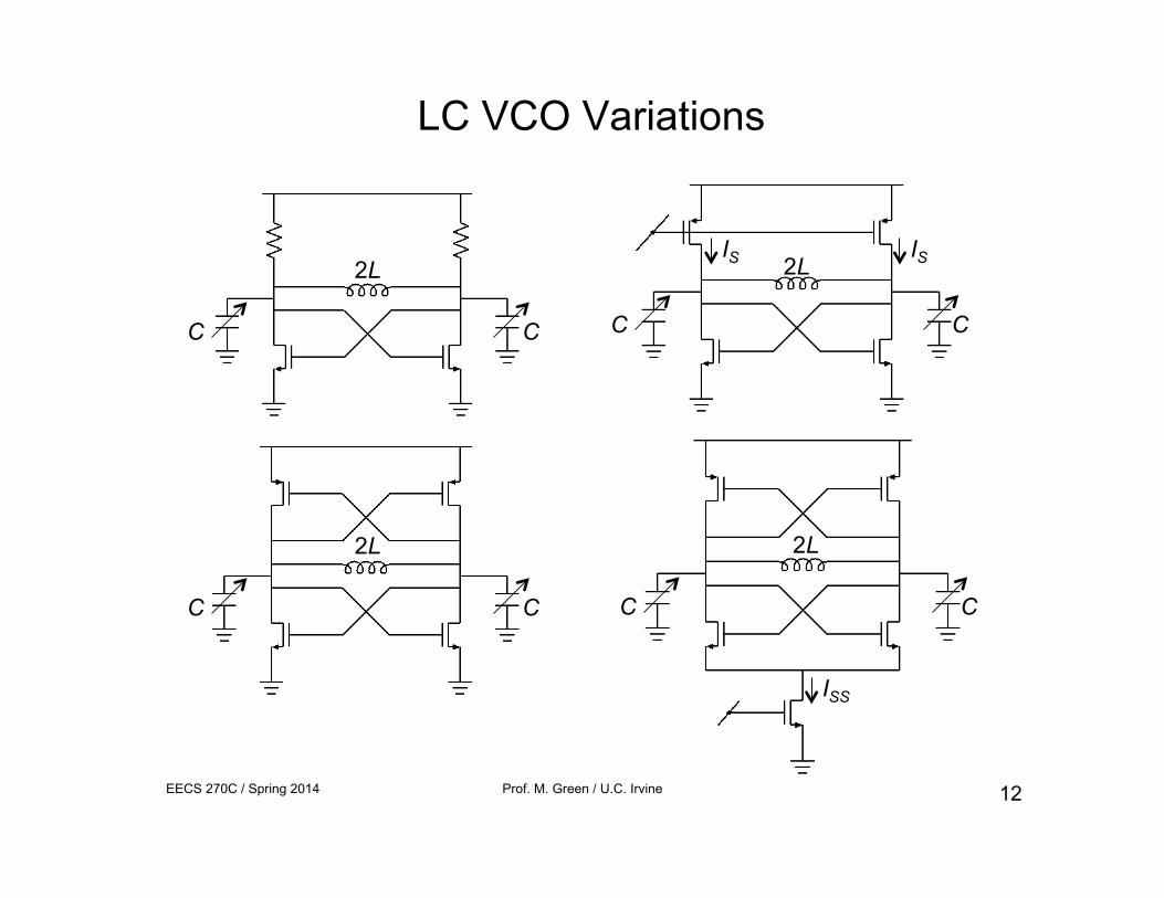
LC VCO Variations
2L
C C
2L
C C
2L
C C
ISS
2L
C C
IS IS

EECS 270C / Spring 2014 Prof. M. Green / U.C. Irvine 13
1. ideal capacitor load
2. CML buffer load
Effect of CML Loading
1.
3.8 Ω 1 nH
400 fF 400 fF
Cg = 108fF
1 nH 3.8 Ω
400 fF 400 fF 108 fF 108 fF
2.

EECS 270C / Spring 2014 Prof. M. Green / U.C. Irvine 14
Substantial parallel loss at high frequencies ⇒ weakens VCO’s tendency to oscillate
(note p < z) where:
€
Yin = jωCgs + jωCgd A0 ⋅1+ jω / z1+ jω / p
€
A0 = 1+ gmR
€
1/ p = CL +Cgd( )R
€
1/ z =CLRA0
€
Re Yin( ) = A0Cgdω2 ⋅
1 p −1 z
1+ ω p( )2
CML Buffer Input Admittance (1)
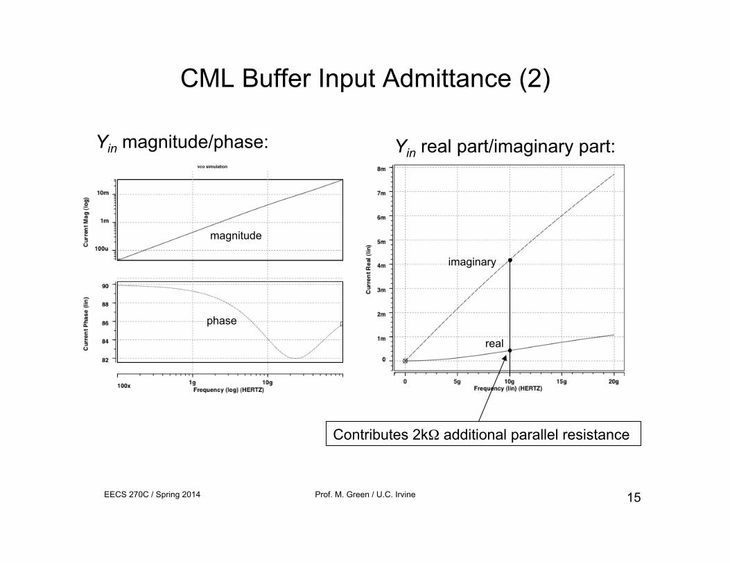
EECS 270C / Spring 2014 Prof. M. Green / U.C. Irvine 15
Yin magnitude/phase: Yin real part/imaginary part:
magnitude
phase
imaginary
real
Contributes 2kΩ additional parallel resistance
CML Buffer Input Admittance (2)

EECS 270C / Spring 2014 Prof. M. Green / U.C. Irvine 16
imaginary
real
Contributes negative parallel resistance
Cg = 108 fF
3.8 nH
3.8 Ω 1 nH
400 fF 400 fF
CML Buffer Input Admittance (3)
3. CML tuned buffer load

EECS 270C / Spring 2014 Prof. M. Green / U.C. Irvine 17
Loading VCO with tuned CML buffer allows negative real part at high frequencies ⇒ more robust oscillation!
ideal capacitor load
CML buffer load
CML tuned buffer load
CML Buffer Input Admittance (4)
Cg = 108 fF
3.8 nH
3.8 Ω 1 nH
400 fF 400 fF

EECS 270C / Spring 2014 Prof. M. Green / U.C. Irvine 18
Differential Control of LC VCO
Differential VCO control is preferred to reduce VC noise coupling into PLL output.

EECS 270C / Spring 2014 Prof. M. Green / U.C. Irvine 19
Ring Oscillator LC Oscillator
– slower – low Q ⇒ more jitter generation + Control voltage can be applied differentially + Easier to design; behavior more predictable + Less chip area
+ faster + high Q ⇒ less jitter generation – Control voltage applied single-ended – Inductors & varactors make design more difficult and behavior less predictable – More chip area (inductor)
Oscillator Type Comparison
EECS 270C / Spring 2014 Prof. M. Green / U.C. Irvine 20
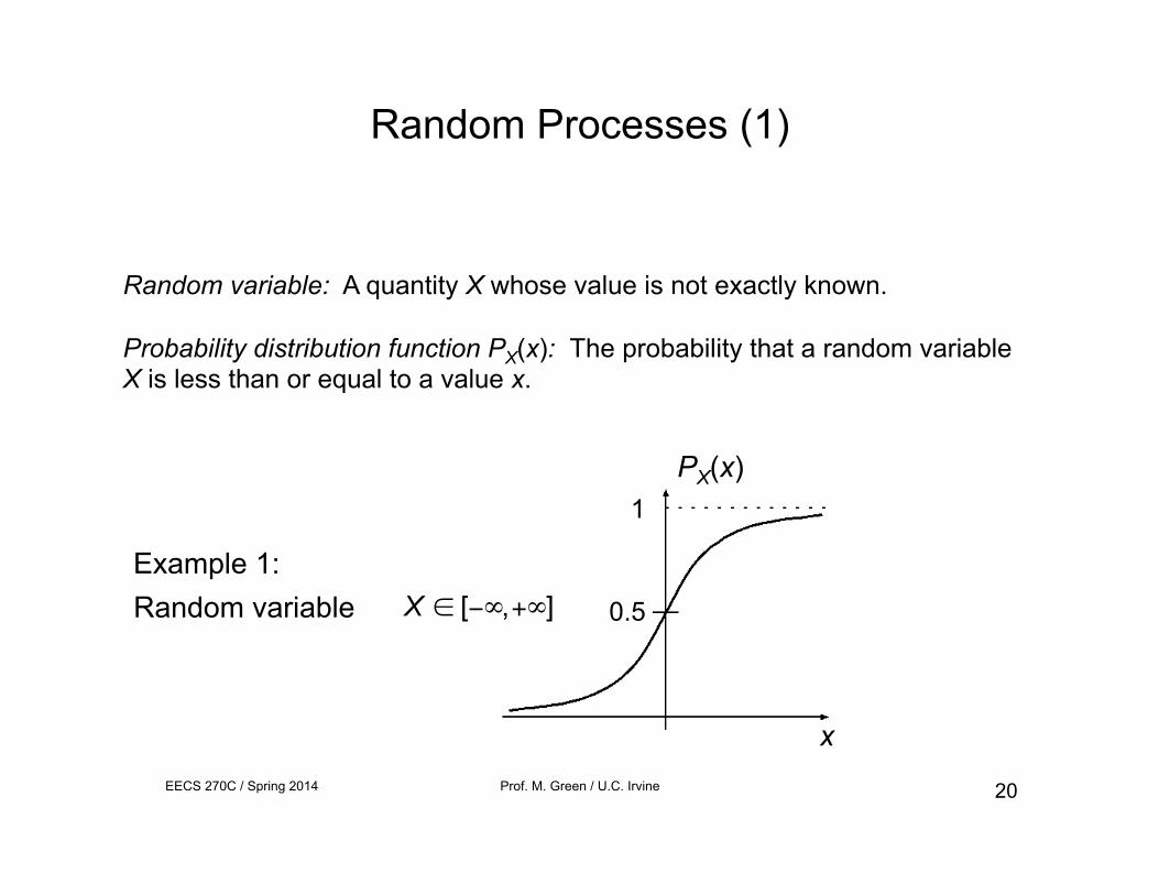
Random Processes (1)
Random variable: A quantity X whose value is not exactly known. Probability distribution function PX(x): The probability that a random variable X is less than or equal to a value x.
0.5
1
x
PX(x)
Example 1:
€
X ∈ [−∞,+∞]Random variable

EECS 270C / Spring 2014 Prof. M. Green / U.C. Irvine 21
0.5
1
x
PX(x)
x1 x2
€
P X ∈ [x1,x2]( ) = P(x2) −P(x1)
Probability of X within a range is straightforward:
If we let x2-x1 become very small …
Random Processes (2)

EECS 270C / Spring 2014 Prof. M. Green / U.C. Irvine 22
Probability density function pX(x): Probability that random variable X lies within the range of x and x+dx.
€
pX (x) ⋅dx = PX (x + dx) −PX (x)
€
⇒ pX (x) =dPX (x)
dx
0.5
1
x
PX(x)
x
pX(x)
dx
€
P X ∈ x1,x2[ ]( ) = pX (x) dxx1
x2∫
Random Processes (3)

EECS 270C / Spring 2014 Prof. M. Green / U.C. Irvine 23
Expectation value E[X]: Expected (mean) value of random variable X over a large number of samples.
€
E[X ] ≡ X = x ⋅pX (x)dx−∞
+∞
∫
Mean square value E[X2]: Mean value of the square of a random variable X2 over a large number of samples.
€
E[X 2] = x2 ⋅pX (x)dx−∞
+∞
∫
Variance:
€
E (X − X )2[ ] ≡σ 2 = x − X( )2pX (x)dx
−∞
+∞
∫
Standard deviation:
€
σ = E (X − X )2[ ]
Random Processes (4)

EECS 270C / Spring 2014 Prof. M. Green / U.C. Irvine 24
Gaussian Function
€
f (x) =1
σ 2πexp −(x − X )2
2σ 2
%
& ' '
(
) * *
x
€
f (x)
€
X
€
1σ 2π
€
0.607σ 2π
€
X −σ
€
X +σ
2σ
€
f (x)dx = 1−∞
+∞
∫
1. Provides a good model for the probability density functions of many random phenomena.
2. Can be easily characterized mathematically . 3. Combinations of Gaussian random variables are themselves
Gaussian.
€
σ,X ( )

EECS 270C / Spring 2014 Prof. M. Green / U.C. Irvine 25
Joint Probability (1)
€
P X ∈ x,x + dx[ ] and Y ∈ y,y + dy[ ]( ) = pX (x) ⋅pY (y) ⋅dx dy
€
P(x,y) ≡ P X ≤ x and Y ≤ y( )
If X and Y are statistically independent (i.e., uncorrelated):
Consider 2 random variables:

EECS 270C / Spring 2014 Prof. M. Green / U.C. Irvine 26
Consider sum of 2 random variables:
€
Z = X +Y
x
y
€
x + y = z0
€
x + y = z0 + dz
dx
dy = dz
€
P Z ∈ z0, z0 + dz[ ]( ) = pX (x)pY (y) dx dystrip∫∫
€
= pX (x)pY (z0 − x) dx−∞
∞
∫% & ' (
) * dz
€
pZ (z0)
determined by convolution of pX and pY.
Joint Probability (2)

EECS 270C / Spring 2014 Prof. M. Green / U.C. Irvine 27
*
Example: Consider the sum of 2 non-Gaussian random processes:
Joint Probability (3)
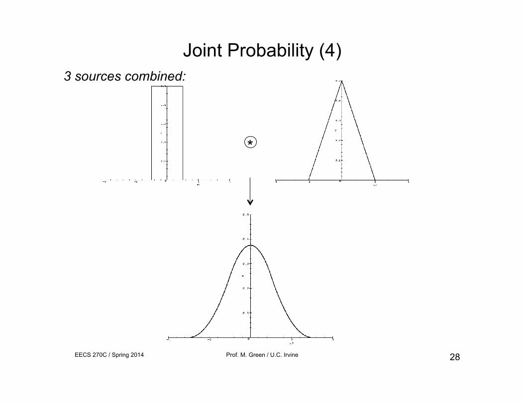
EECS 270C / Spring 2014 Prof. M. Green / U.C. Irvine 28
3 sources combined:
*
Joint Probability (4)

EECS 270C / Spring 2014 Prof. M. Green / U.C. Irvine 29
4 sources combined:
*
Joint Probability (5)

EECS 270C / Spring 2014 Prof. M. Green / U.C. Irvine 30
Central Limit Theorem: Superposition of random variables tends toward normality.
Noise sources
Joint Probability (6)

EECS 270C / Spring 2014 Prof. M. Green / U.C. Irvine 31
Fourier transform of Gaussians:
€
pX (x) =1
σ X 2πexp −(x − X )2
2σ X2
%
&
' '
(
)
* *
€
PX (ω) = exp −12σ X
2ω2%
& '
(
) * F
€
P Z ∈ z0,z0 + dz[ ]( ) = pX (x)pY (z0 − x) dx−∞
∞
∫& ' ( )
* + dz
Recall:
€
pZ (z0) = pX (x)pY (z0 − x) dx−∞
∞
∫ F
€
PZ (ω) =PX (ω) ⋅PY (ω)
€
= exp −12σ X
2ω2%
& '
(
) * ⋅exp −
12σY
2ω2%
& '
(
) *
€
= exp −12
(σ X2 +σ X
2 )ω2%
& '
(
) *
F -1
€
pZ (z) =1
2π σ X2 +σY
2( )exp −(z − Z)2
2 σ X2 +σY
2( )
%
&
' '
(
)
* *
Variances of sum of random normal processes add.

EECS 270C / Spring 2014 Prof. M. Green / U.C. Irvine 32
Autocorrelation function RX(t1,t2): Expected value of the product of 2 samples of a random variable at times t1 & t2.
€
RX (t1,t2 ) = E X (t1) ⋅X (t2 )[ ]
For a stationary random process, RX depends only on the time difference
€
RX (τ ) = E X (t) ⋅X (t +τ )[ ] for any t
€
RX (0) =σ 2Note €
τ = t1 − t2
Power spectral density SX(ω):
€
SX (ω) = E X (t) ⋅e− jωtdt−∞
+∞
∫2'
(
) ) )
*
+
, , ,
SX(ω) given in units of [dBm/Hz]

EECS 270C / Spring 2014 Prof. M. Green / U.C. Irvine 33
€
RX (τ ) =1
2πSX (ω) ⋅e jωτdω
−∞
∞
∫
Relationship between spectral density & autocorrelation function:
€
⇒ RX (0) =σ 2 =1
2πSX (ω)dω
−∞
∞
∫
Example 1: white noise
ω
€
SX (ω)
€
RX (τ )
τ
infinite variance (non-physical)
€
SX ω( ) = K
€
RX (τ ) =K2π
⋅δ t( )

EECS 270C / Spring 2014 Prof. M. Green / U.C. Irvine 34
Example 2: band-limited white noise
€
SX (ω)
ω
€
ωp
€
−ωp
€
RX (τ )
€
σ 2 =12
Kωp
€
RX (τ ) =σ 2e−ω p τ τ
€
K
€
SX ω( ) =K
1+ω2
ωp2
x
€
pX (x)
€
−σ
€
+σ
For parallel RC circuit capacitor voltage noise:
€
K =in
2
Δf⋅R2 = 2kBTR
€
ωp =1
RC
€
σVC2 =
kBTC

EECS 270C / Spring 2014 Prof. M. Green / U.C. Irvine 35
Random Jitter (Time Domain)
Experiment:
data source
CDR (DUT) analyzer
CLK
DATA RCK

EECS 270C / Spring 2014 Prof. M. Green / U.C. Irvine 36
Jitter Accumulation (1)
€
Tosc =1
fosc
Free-running oscillator output
Histogram plots
Experiment: Observe N cycles of a free-running VCO on an oscilloscope over a long measurement interval using infinite persistence.
NT
τ1 τ2 τ3 τ4
trigger
€
σ1
€
σ 2
€
σ 3
€
σ 4

EECS 270C / Spring 2014 Prof. M. Green / U.C. Irvine 37
Observation: As τ increases, rms jitter increases.
€
τ
€
στ2
proportional to τ2
proportional to τ
€
Jitter Accumulation (2)

EECS 270C / Spring 2014 Prof. M. Green / U.C. Irvine 38
Noise Spectral Density (Frequency Domain)
fosc fosc+Δf
Sv(f)
Ltotal (Δf ) =10 logP1Hz fosc +Δf( )
Ptotal
"
#
$$
%
&
''
€
dBcHz[ ]
Δf (log scale)
Ltotal Δf( )
1/Δf2 region (-20dBc/Hz/decade)
Power spectral density of oscillation waveform:
€
dBmHz[ ]
Single-sideband spectral density:
Ltotal includes both amplitude and phase noise
Ltotal(Δf) given in units of [dBc/Hz]
1/Δf3 region (-30dBc/Hz/decade)

EECS 270C / Spring 2014 Prof. M. Green / U.C. Irvine 39
€
ωr + Δω
€
ωr
Noise Analysis of LC VCO (1)
active circuitry
C L R -R C L
+
_ vc
inR
€
Z( jω) =jωL
1− ωωr
$
% &
'
( )
2
€
ωr =1LC
€
Z j ωr + Δω( )[ ] =j ωr + Δω( )L
1−ωr
2 + 2ωrΔω + Δω( )2
ωr2
≈ jL ⋅ ωr2
2Δω
Consider frequencies near resonance:
€
Q =RωrL
noise from resistor
€
ωrL =RQ⇒ Z j ωr + Δω( )[ ] ≈ j R
2Q⋅ωr
Δω
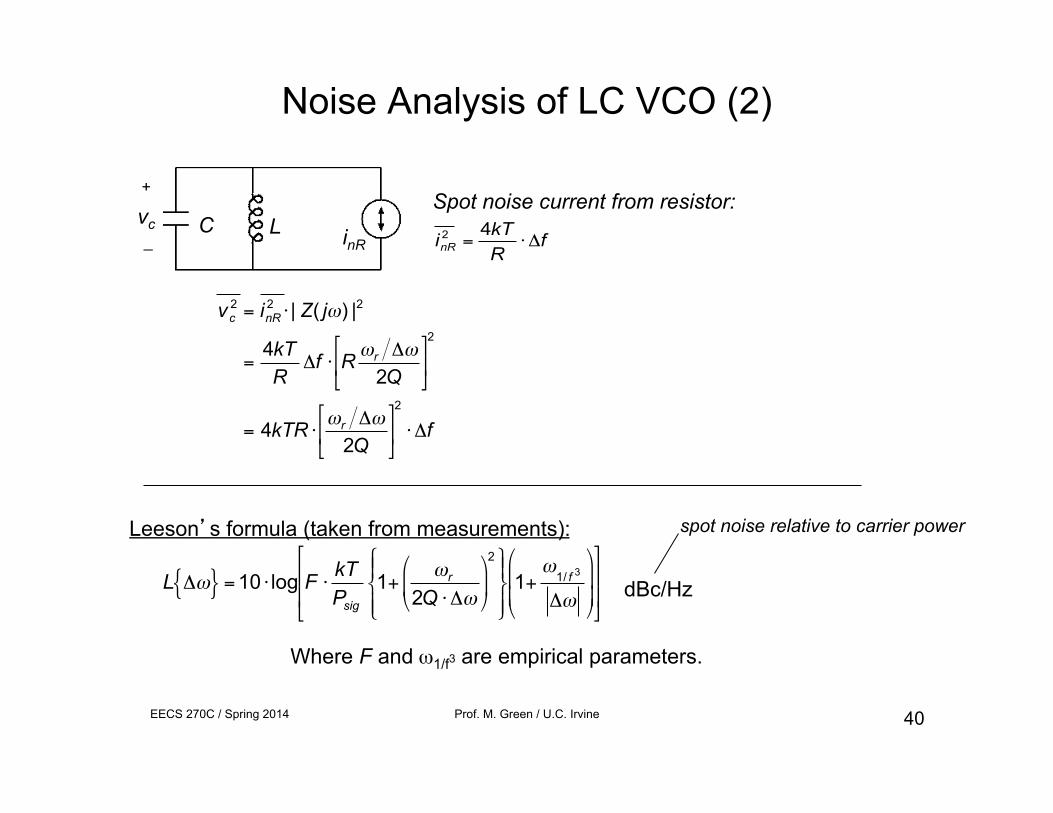
EECS 270C / Spring 2014 Prof. M. Green / U.C. Irvine 40
Spot noise current from resistor:
€
inR2 =
4kTR
⋅ ΔfC L
+
_ vc
inR
€
vc2 = inR
2 ⋅ | Z( jω) |2
=4kTR
Δf ⋅ R ωr Δω2Q
%
& '
(
) *
2
= 4kTR ⋅ωr Δω
2Q%
& '
(
) *
2
⋅ Δf
Noise Analysis of LC VCO (2)
€
L Δω{ } = 10 ⋅ log F ⋅kTPsig
1+ωr
2Q ⋅ Δω
%
& '
(
) *
2+ , -
. -
/ 0 -
1 - 1+
ω1/ f 3
Δω
%
&
' '
(
)
* *
2
3
4 4
5
6
7 7
Leeson’s formula (taken from measurements):
Where F and ω1/f3 are empirical parameters.
dBc/Hz
spot noise relative to carrier power

EECS 270C / Spring 2014 Prof. M. Green / U.C. Irvine 41
Oscillator Phase Disturbance Current impulse Δq/Δt
_ + Vosc
t t
ip(t)
Vosc(t) Vosc(t)
Vosc jumps by Δq/C
• Effect of electrical noise on oscillator phase noise is time-variant. • Current impulse results in step phase change (i.e., an integration). ⇒ current-to-phase transfer function is proportional to 1/s
ip(t)
€
τ 1
€
τ 2
€
Δφ = 0
€
Δφ < 0
ip(t)

EECS 270C / Spring 2014 Prof. M. Green / U.C. Irvine 42
Impulse Sensitivity Function (1) The phase response for a particular noise source can be determined at each point τ over the oscillation waveform.
€
Γ(τ ) ≡ Δφ(τ )Δq
⋅qmaxImpulse sensitivity function (ISF):
€
= C ⋅Vmax(normalized to signal amplitude)
change in phase charge in impulse
t
τ
€
Vosc (t)
€
Γ(τ )
€
Vmax
Example 1: sine wave
t
τ
€
Vosc (t)
€
Γ(τ )
Example 2: square wave
Note Γ has same period as Vosc.

EECS 270C / Spring 2014 Prof. M. Green / U.C. Irvine 43
Impulse Sensitivity Function (2)
€
H(s)h(t)
€
iin
€
φout
Recall from network theory:
€
Φout (s)Iin (s)
= H(s)LaPlace transform:
€
φout (t) = h(t,τ ) ⋅ iin (τ ) dτ0
t
∫Impulse response:
time-variant impulse response
€
Γ(τ ) ≡ Δφ(τ )Δq
⋅qmax ⇒ Δφ(τ ) =Γ(τ )qmax
⋅ ΔqRecall:
ISF convolution integral:
€
φ(t) =Γ(τ )qmax0
t
∫ ⋅u(t −τ ) ⋅ i (τ ) ⋅dτ[ ] =Γ(τ )qmax0
t
∫ ⋅ i (τ ) ⋅dτ
from Δq
€
= 1 for τ ∈ (0,t)
€
Γ(τ ) = ck cos kωoscτ +θk( )k=0
∞
∑
Γ can be expressed in terms of Fourier coefficients:

EECS 270C / Spring 2014 Prof. M. Green / U.C. Irvine 44
Case 1: Disturbance is sinusoidal:
€
i (t) = I0 cos mωosc + Δω( )t[ ] , m = 0, 1, 2, …
€
=I0
2qmax
ck
sin (k + m)ωosc + Δω[ ]t +θk{ }(k + m)ωosc + Δω
+sin (k −m)ωosc + Δω[ ]t +θk{ }
(k −m)ωosc + Δω
& ' (
) (
* + (
, ( k=0
∞
∑
negligible significant only for m = k
(Any frequency can be expressed in terms of m and Δω.)
€
φ(t) =I0
qmax
ck cos kωoscτ +θk( ) ⋅cos mωosc + Δω( )t[ ]{ }dτ0
t
∫k=0
∞
∑
€
Γ(τ )
€
≈I0
2qmax
⋅cm ⋅sin Δω t +θk( )
Δω
Impulse Sensitivity Function (3)

EECS 270C / Spring 2014 Prof. M. Green / U.C. Irvine 45
ω
I
2ωosc
Δω
φ
€
×I0
2qmax
c0
ω1
€
×I0
2qmax
c1
ω1
€
×I0
2qmax
c2
ω1
Impulse Sensitivity Function (4)
€
φ(t) ≈ I02qmax
⋅cm ⋅sin Δω t +θk( )
Δω⇒φ2 =
I02
8qmax2
⋅cm
2
Δω( )2
Current-to-phase frequency response:
ωosc ωosc-ω1
ω1
ω1 ωosc+ω1 2ωosc-ω1 2ωosc+ω1
For
€
i (t) = I0 cos mωosc + Δω( )t[ ]

EECS 270C / Spring 2014 Prof. M. Green / U.C. Irvine 46
€
×c0
€
×c1
€
in2
Δf
€
4kTγgm
ω ωosc 2ωosc
€
×c2
Case 2: Disturbance is stochastic:
Impulse Sensitivity Function (5)
MOSFET current noise:
thermal noise 1/f
noise
€
in2(f )Δf
= 4kTγgm + gm2 Kf
CgfA2/Hz
€
in
€
φ2 Δf ≈ in2 Δf
8qmax2
⋅cm
2
Δω( )2
€
Sφ Δω( )
Δω
€
in2
Δf
ω ωosc 2ωosc
€
×c0
€
gm2 2π ⋅Kf
Cgωthermal noise
1/f noise
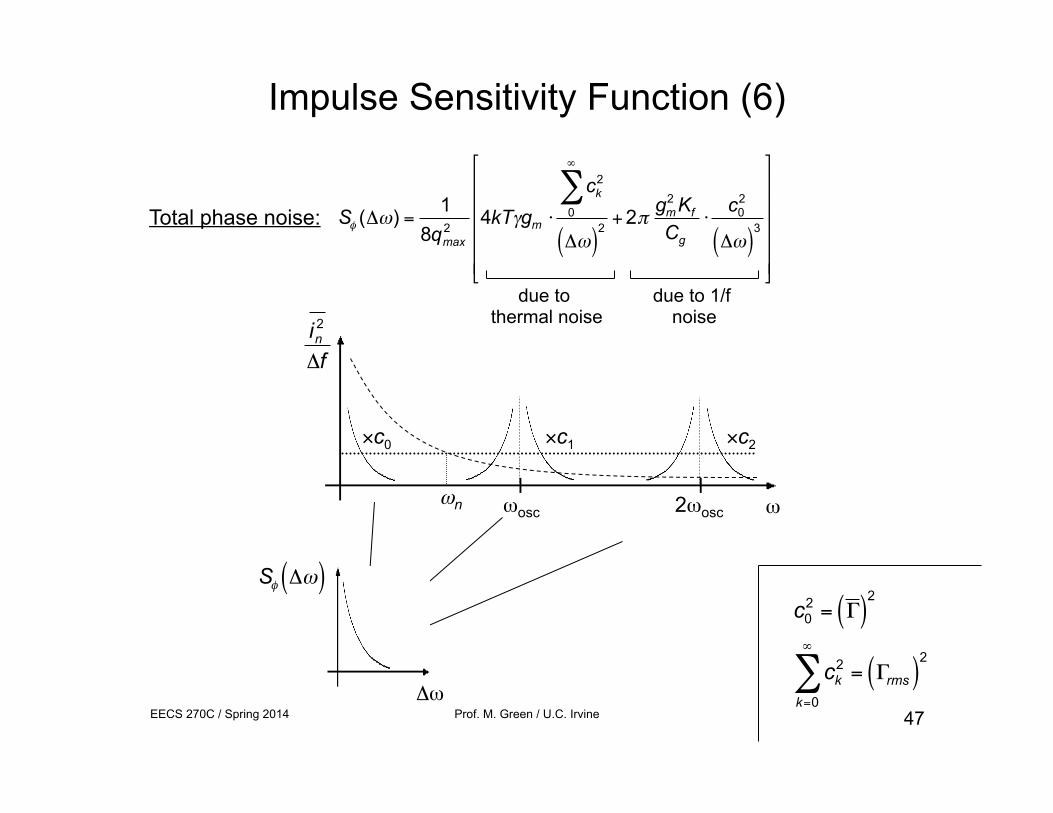
EECS 270C / Spring 2014 Prof. M. Green / U.C. Irvine 47
Impulse Sensitivity Function (6)
€
Sφ Δω( )
Δω
€
×c0
€
×c1
€
in2
Δf
ω ωosc 2ωosc
€
×c2
€
Sφ (Δω) =1
8qmax2
4kTγgm ⋅
ck2
0
∞
∑
Δω( )2
+ 2π gm2 Kf
Cg
⋅c0
2
Δω( )3
*
+
, , , , ,
-
.
/ / / / /
due to 1/f noise
due to thermal noise
Total phase noise:
€
c02 = Γ ( )
2
ck2
k=0
∞
∑ = Γrms( )2
ωn

EECS 270C / Spring 2014 Prof. M. Green / U.C. Irvine 48
Impulse Sensitivity Function (7)
€
Sφ (Δω) =1
8qmax2
4kTγgm ⋅Γrms( )
2
Δω( )2
+ 2π gm2 Kf
Cg
⋅Γ ( )
2
Δω( )3
)
*
+ + +
,
-
.
.
.
€
4kTγgm ⋅Γrms( )
2
Δω( )2
= 2π gm2 Kf
Cg
⋅Γ ( )
2
Δω( )3
€
⇒
€
Δωn ,phase =π
2kT⋅
gm
γCg
⋅ΓΓrms
(
) * *
+
, - -
2
noise corner frequency ωn
Δω (log scale)
€
Sφ Δω( ) (dBc/Hz)
€
Δωn ,phase
1/(Δω)3 region: −30 dBc/Hz/decade
1/(Δω)2 region: −20 dBc/Hz/decade

EECS 270C / Spring 2014 Prof. M. Green / U.C. Irvine 49
t
τ
€
Vosc (t)
€
Γ(τ )
t
τ
€
Vosc (t)
€
Γ(τ )
Example 1: sine wave Example 2: square wave
Impulse Sensitivity Function (8)
Example 3: asymmetric square wave
t
τ
€
Vosc (t)
€
Γ(τ )
€
Γ > 0 ⇒ will generate more 1/(Δω)3 phase noise
€
Γrms is higher ⇒ will generate more 1/(Δω)2 phase noise

EECS 270C / Spring 2014 Prof. M. Green / U.C. Irvine 50
Impulse Sensitivity Function (9)
Effect of current source in LC VCO:
Vosc + _
Due to symmetry, ISF of this noise source contains only even-order coefficients − c0 and c2 are dominant.
⇒ Noise from current source will contribute to phase noise of differential waveform.

EECS 270C / Spring 2014 Prof. M. Green / U.C. Irvine 51
Impulse Sensitivity Function (10)
ID varies over oscillation waveform
€
in2
Δf= 4kTγgm (t)
= (4kTγ ) ⋅ µCoxWL⋅ VGS (t) −Vt( )
&
' (
)
* +
Same period as oscillation
€
in02
Δf= (4kTγ ) ⋅ µCox
WL⋅ VGS(DC ) −Vt( )
&
' (
)
* + Let
Then
€
in2
Δf=
in02
Δf⋅α(t)
€
α(t) =VGS (t) −Vt
VGS(DC ) −Vtwhere
€
Γeff (τ ) = Γ(τ ) ⋅α(τ )We can use

EECS 270C / Spring 2014 Prof. M. Green / U.C. Irvine 52
ISF Example: 3-Stage Ring Oscillator
M1A M1B M2A M2B M3A M3B
MS1 MS2 MS3
R1A R1B R2A R2B R3A R3B + Vout −
fosc = 1.08 GHz PD = 11 mW

EECS 270C / Spring 2014 Prof. M. Green / U.C. Irvine 53
ISF of Diff. Pairs
ISF by tx6 for differential ring osc
-5
-4
-3
-2
-1
0
1
2
3
0 1 2 3 4 5 6 7
Radian
ISF
by t
x6
ISF by tx5 for differential ring osc
-5
-4
-3
-2
-1
0
1
2
3
0 1 2 3 4 5 6 7
Radian
ISF
by t
x5
ISF by tx4 for differential ring osc
-5
-4
-3
-2
-1
0
1
2
3
0 1 2 3 4 5 6 7
Radian
ISF
by t
x4
ISF by tx3 for differential ring osc
-5
-4
-3
-2
-1
0
1
2
3
0 1 2 3 4 5 6 7
Radian
ISF
by t
x3
ISF by tx2 for differential ring osc
-5
-4
-3
-2
-1
0
1
2
3
0 1 2 3 4 5 6 7
Radian
ISF
by t
x2
ISF by tx1 for 3stage differential ring osc
-5
-4
-3
-2
-1
0
1
2
3
0 1 2 3 4 5 6 7
Radian
ISF
by t
x1
€
ΓM1A
€
ΓM1B
€
ΓM2A
€
ΓM2B
€
ΓM3A
€
ΓM3B
€
Γrms = 1.86Γ = −0.26
for each diff. pair transistor

EECS 270C / Spring 2014 Prof. M. Green / U.C. Irvine 54
ISF of Resistors
€
ΓR1A
€
ΓR2A
€
ΓR3A
€
Γrms = 1.72Γ = −0.16
for each resistor

EECS 270C / Spring 2014 Prof. M. Green / U.C. Irvine 55
ISF of Current Sources
ISF by tail tx3 for differential ring osc
-2
-1.5
-1
-0.5
0
0.5
1
1.5
2
0 1 2 3 4 5 6 7
Radian
ISF
by t
ail t
x3
ISF by tail tx2 for differential ring osc
-2
-1.5
-1
-0.5
0
0.5
1
1.5
2
0 1 2 3 4 5 6 7
Radian
ISF
by t
ail t
x2
ISF by tail tx1 for differential ring osc
-2
-1.5
-1
-0.5
0
0.5
1
1.5
2
0 1 2 3 4 5 6 7
Radian
ISF
by t
ail t
x1
€
ΓMS1
€
ΓMS2
€
ΓMS3
ISF shows double frequency due to source-coupled node connection.
€
Γrms = 1.00Γ = −0.12
for each current source transistor

EECS 270C / Spring 2014 Prof. M. Green / U.C. Irvine 56
Phase Noise Calculation
Using: Cout = 1.13 pF Vout = 601 mV p-p qmax = 679 fC
€
L Δf{ } = 6 ⋅Γrms(dp)
2
8π 2Δf 2⋅4kTγ gm(dp)
qmax2
+ 6 ⋅Γrms(res)
2
8π 2Δf 2⋅4kT R
qmax2
+ 3 ⋅Γrms(cs)
2
8π 2Δf 2⋅4kTγ gm(cs)
qmax2
€
322Δf 2
€
122Δf 2
€
70Δf 2
€
⇒ L Δf{ } =514Δf 2 = −112 dBc/Hz @ Δf = 10 MHz

EECS 270C / Spring 2014 Prof. M. Green / U.C. Irvine 57
Phase Noise vs. Amplitude Noise (1)
€
Vosc (t) = Vc +v (t)[ ] ⋅exp j ωosct +φ(t)( )[ ]
ωosct
φ v vφ Spectrum of Vosc would
include effects of both amplitude noise v(t) and phase noise φ(t).
How are the single-sideband noise spectrum Ltotal(Δω) and phase spectral density Sφ(ω) related?

EECS 270C / Spring 2014 Prof. M. Green / U.C. Irvine 58
Phase Noise vs. Amplitude Noise (2)
t t
i(t) i(t)
Vc(t) Vc(t)
0=Δtosc
qt
ωΔ
=Δ
Recall that an input current impulse causes an enduring phase perturbation and a momentary change in amplitude:
Amplitude impulse response exhibits an exponential decay due to the natural amplitude limiting of an oscillator ...
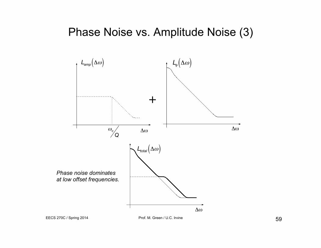
EECS 270C / Spring 2014 Prof. M. Green / U.C. Irvine 59
Δω
€
Lamp Δω( )
€
ωcQ
Δω
+
Δω
€
Ltotal Δω( )
Phase noise dominates at low offset frequencies.
Phase Noise vs. Amplitude Noise (3)
€
Lφ Δω( )
Δω

EECS 270C / Spring 2014 Prof. M. Green / U.C. Irvine 60
€
Vosc (t) = Vc +v (t)( ) ⋅cos ωosct +φ(t)( )≈ Vc +v (t)( ) ⋅ cos(ωosct) −φ(t) ⋅sin(ωosct)[ ]= Vc cos(ωosct) −φ(t) ⋅Vc sin(ωosct) +v (t) ⋅cos(ωosct)
ωosc Phase & amplitude noise can’t be distinguished in a signal.
Sv(ω)
Amplitude limiting will decrease amplitude noise but will not affect phase noise.
Phase Noise vs. Amplitude Noise (4)
noiseless oscillation waveform
phase noise
component
amplitude noise
component
phase noise
amplitude noise
ω
EECS 270C / Spring 2014 Prof. M. Green / U.C. Irvine 61
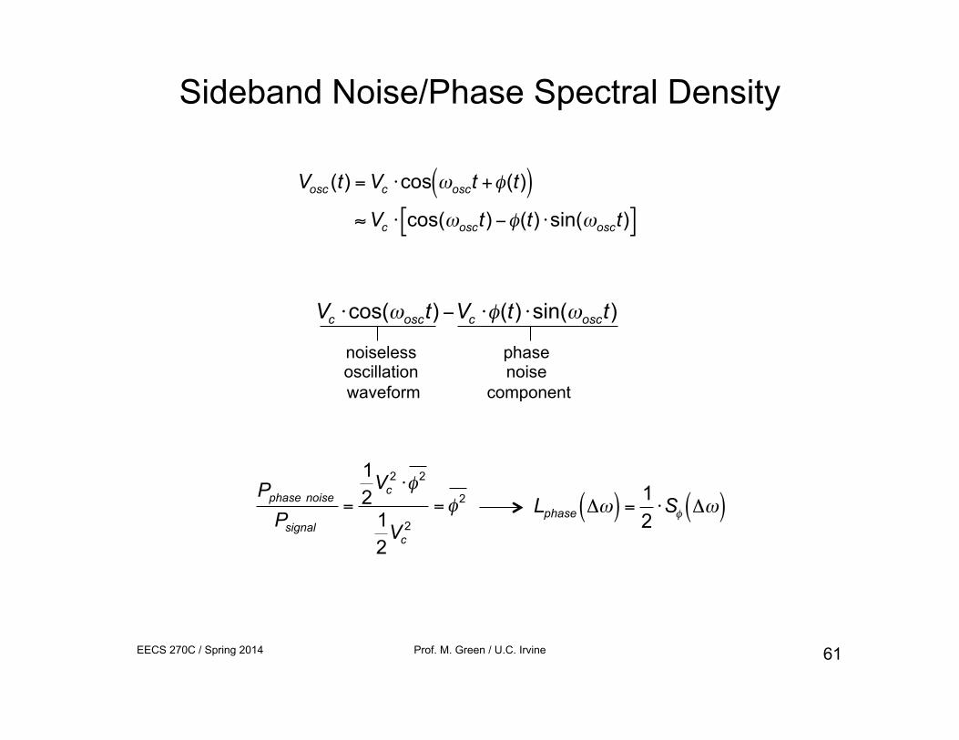
Sideband Noise/Phase Spectral Density
€
Vosc (t) = Vc ⋅cos ωosct +φ(t)( )≈Vc ⋅ cos(ωosct) −φ(t) ⋅sin(ωosct)[ ]
€
Vc ⋅cos(ωosct) −Vc ⋅φ(t) ⋅sin(ωosct)
€
Pphase noise
Psignal
=
12
Vc2 ⋅φ2
12
Vc2
=φ2
€
Lphase Δω( ) =12⋅Sφ Δω( )
noiseless oscillation waveform
phase noise
component

EECS 270C / Spring 2014 Prof. M. Green / U.C. Irvine 62
Jitter/Phase Noise Relationship (1)
€
στ2 ≡
1ωosc
2⋅E φ(t +τ ) −φ(t)[ ]
2) * +
, - .
€
=1
ωosc2
⋅ E φ2(t +τ )[ ] + E φ2 (t)[ ] −2E φ(t) ⋅φ(t +τ )[ ]{ }
€
Rφ (0)
€
Rφ (0)
€
2Rφ (τ )autocorrelation functions
€
Rφ (τ ) =1
2πSϕ (Δω) ⋅e j (Δω )τd(Δω)
−∞
∞
∫Recall Rφ and Sφ(Δω) are a Fourier transform pair:
€
⇒στ2 =
2ωosc
2⋅ Rφ (0) −Rφ (τ )[ ]
NT

EECS 270C / Spring 2014 Prof. M. Green / U.C. Irvine 63
€
Rφ (0) =1
2πSφ (Δω)d(Δω)
−∞
∞
∫
Rφ (τ ) =1
2πSφ (Δω) ⋅e j (Δω )τd(Δω)
−∞
∞
∫
€
στ2 =
1πωosc
2⋅ Sφ (Δω) 1−e j (Δω )τ( )−∞
∞
∫ d(Δω)
=1
πωosc2
⋅ Sφ (Δω) 1−cos(Δωτ ) − j sin(Δωτ )[ ]−∞
∞
∫ d(Δω)
=4
πωosc2
⋅ Sφ (Δω) ⋅sin2 Δωτ2
,
- .
/
0 1
0
∞
∫ d(Δω)
Jitter/Phase Noise Relationship (2)

EECS 270C / Spring 2014 Prof. M. Green / U.C. Irvine 64
Let
€
Sφ (Δω) =a
(Δω)2
€
στ2 =
4πωosc
2⋅
a(Δω)2
⋅sin2 (Δω)τ2
(
) *
+
, -
0
∞
∫ d(Δω)
€
=4
πωosc2
⋅aπτ
4
€
=a
ωosc2
⋅τ
Let
€
Sφ (Δω) =b
(Δω)3
€
στ2 =
4πωosc
2⋅
b(Δω)3
⋅sin2 (Δω)τ2
(
) *
+
, -
ε
∞
∫ d(Δω)
€
= ζ ⋅ τ 2
Consistent with jitter accumulation measurements!
Jitter/Phase Noise Relationship (3)
Jitter from 1/(Δω) noise: 2 Jitter from 1/(Δω) noise: 3
^
^
^
^
€
=a
fosc2⋅τ where a ≡ (2π )2 ⋅a^

EECS 270C / Spring 2014 Prof. M. Green / U.C. Irvine 65
Jitter/Phase Noise Relationship (4)
Δf
€
Sφ Δf( ) (dBc/Hz)
-100
-20dBc/Hz per decade
• Let fosc = 10 GHz • Assume phase noise dominated by 1/(Δω)2
€
Sφ Δf( ) =a
(Δf )2
€
Sφ 2 ⋅106( ) =a
2 ⋅106( )2
= 10−10 ⇒ a = 400
Setting Δf = 2 X 10⁶ and Sφ =10-10:
€
στ2 =
afc
2⋅τ =
400
10 ⋅109( )2⋅τ = 4 ⋅10−18[ ] ⋅τ
€
στ = 2 ⋅10−9[ ] ⋅ τ
Let τ = 100 ps (cycle-to-cycle jitter): ⇒ στ = 0.02ps rms (0.2 mUI rms)
Accumulated jitter:
2 MHz
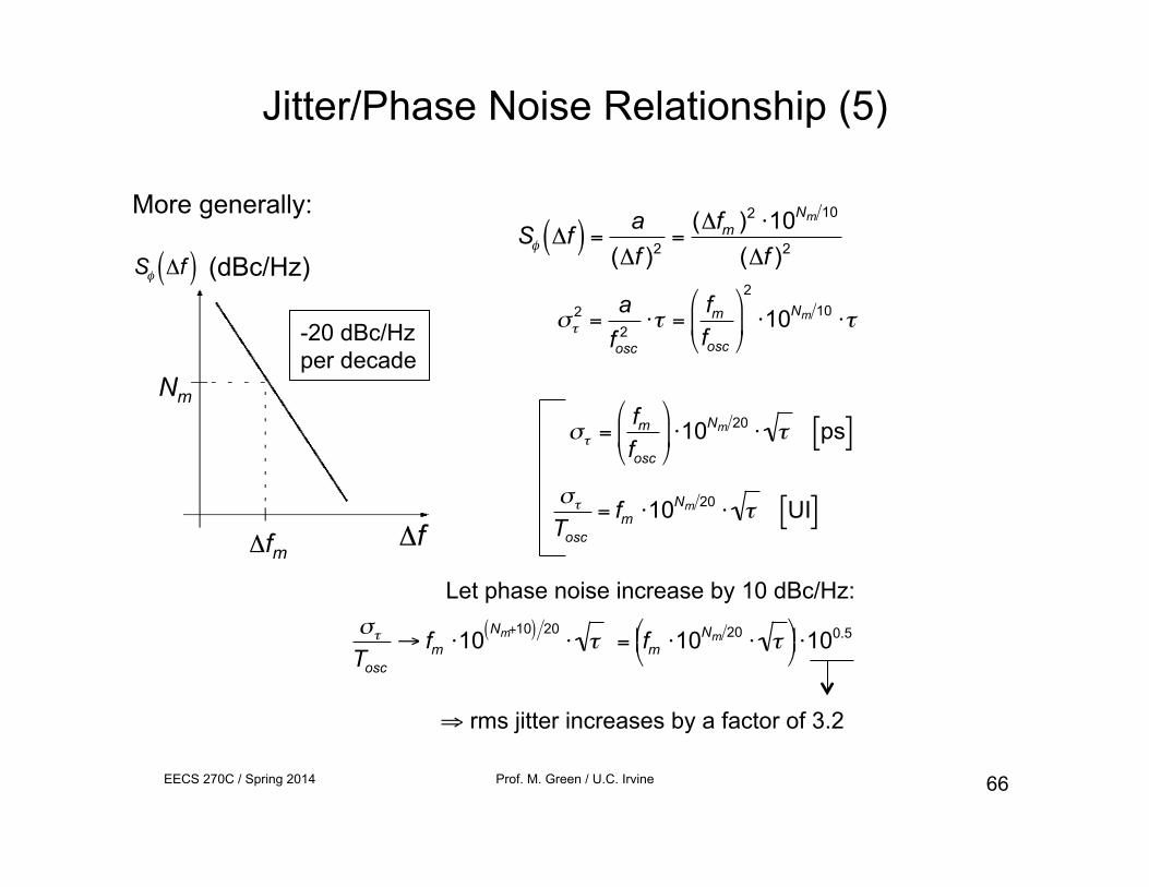
EECS 270C / Spring 2014 Prof. M. Green / U.C. Irvine 66
More generally:
Δf
€
Sφ Δf( ) (dBc/Hz)
Δfm
Nm
-20 dBc/Hz per decade
€
στ2 =
afosc
2⋅τ =
fmfosc
%
& '
(
) *
2
⋅10Nm 10 ⋅τ
€
στ =fmfosc
$
% &
'
( ) ⋅10Nm 20 ⋅ τ ps[ ]
€
στ
Tosc
= fm ⋅10Nm 20 ⋅ τ UI[ ]
€
στ
Tosc
→ fm ⋅10 Nm+10( ) 20⋅ τ = fm ⋅10Nm 20 ⋅ τ&
' ( )
* + ⋅100.5
⇒ rms jitter increases by a factor of 3.2
€
Sφ Δf( ) =a
(Δf )2=
(Δfm )2 ⋅10Nm 10
(Δf )2
Jitter/Phase Noise Relationship (5)
Let phase noise increase by 10 dBc/Hz:

EECS 270C / Spring 2014 Prof. M. Green / U.C. Irvine 67
Jitter Accumulation (1)
Kpd
phase detector
loop filter
€
F (s) Kvco
VCO
€
÷N€
+φin
φout φvco
φfb
€
φout
φε= G(s) = Kpd ⋅F (s) ⋅Kvco
2πs⋅
1N
Open-loop characteristic:
€
φout =NG(s)1+G(s)
⋅φin +1
1+G(s)⋅φvcoClosed-loop characteristic:

EECS 270C / Spring 2014 Prof. M. Green / U.C. Irvine 68
Jitter Accumulation (2)
€
G(s) =IchKvco
N⋅
1s2 (C +Cp )
⋅1+ sCR
1+ sCeq RRecall from Type-2 PLL:
Δω
|G| z p ω0
|1 + G|
-40 dB/decade
Δω
€
Sφ Δω( ) (dBc/Hz)
€
Δωn ,phase
1/(Δω)3 region: −30 dBc/Hz/decade
1/(Δω)2 region: −20 dBc/Hz/decade
Δω
€
φout
φvco
jΔω( )2
1
80 dB/decade
ω0
As a result, the phase noise at low offset frequencies is determined by input noise...
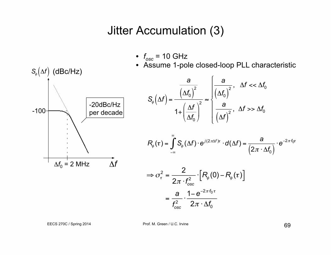
EECS 270C / Spring 2014 Prof. M. Green / U.C. Irvine 69
• fosc = 10 GHz • Assume 1-pole closed-loop PLL characteristic
Jitter Accumulation (3)
Δf
€
Sφ Δf( ) (dBc/Hz)
Δf0 = 2 MHz
-100 -20dBc/Hz per decade
€
Sφ Δf( ) =
a
Δf0( )2
1+ΔfΔf0
$
% &
'
( )
2≈
a
Δf0( )2
, Δf << Δf0
a
Δf( )2
, Δf >> Δf0
+
,
- -
.
- -
€
⇒στ2 =
22π ⋅ fosc
2⋅ Rφ (0) −Rφ (τ )[ ]
=a
fosc2⋅1−e−2π⋅f0τ
2π ⋅Δf0
€
Rφ (τ ) = Sφ (Δf ) ⋅e j (2πΔf )τ ⋅d(Δf ) =a
2π ⋅Δf0( )⋅e−2π⋅f0τ
−∞
∞
∫

EECS 270C / Spring 2014 Prof. M. Green / U.C. Irvine 70
€
a = 4×10²
For large τ:
στ = 0.02 ps rms cycle-to-cycle jitter
Jitter Accumulation (4)
Δf0 = 2 MHz
fosc = 10 GHz
€
στ2 =
afosc
2⋅1−e−2π⋅f0τ
2π ⋅Δf0≈
afosc
2⋅τ
afosc
2⋅
12π (Δf0)
)
* + +
, + +
€
, τ <<1
2π (Δf0)
, τ >>1
2π (Δf0)
For small τ:
€
στ2 (log scale)
τ
€
1(2π ) ⋅ (2 MHz)
€
slope =a
fosc2
στ = 1.4 ps rms Total accumulated jitter

EECS 270C / Spring 2014 Prof. M. Green / U.C. Irvine 71
The primary function of a PLL is to place a bound on cumulative jitter:
τ
€
στ2 (log scale)
€
στ2 (log scale)
proportional to τ (due to thermal noise)
proportional to τ2 (due to 1/f noise)
τ
Jitter Accumulation (5)

EECS 270C / Spring 2014 Prof. M. Green / U.C. Irvine 72
L(Δω) for OC-192 SONET transmitter
Closed-Loop PLL Phase Noise Measurement

EECS 270C / Spring 2014 Prof. M. Green / U.C. Irvine 73
Other Sources of Jitter in PLL
• Clock divider
• Phase detector Ripple on phase detector output can cause high-frequency jitter. This affects primarily the jitter tolerance of CDR.

EECS 270C / Spring 2014 Prof. M. Green / U.C. Irvine 74
Jitter/Bit Error Rate (1)
Histogram showing Gaussian distribution
near sampling point
1UI
Bit error rate (BER) determined by σ and UI …
L R €
2σR
€
2σ L
Eye diagram from sampling oscilloscope
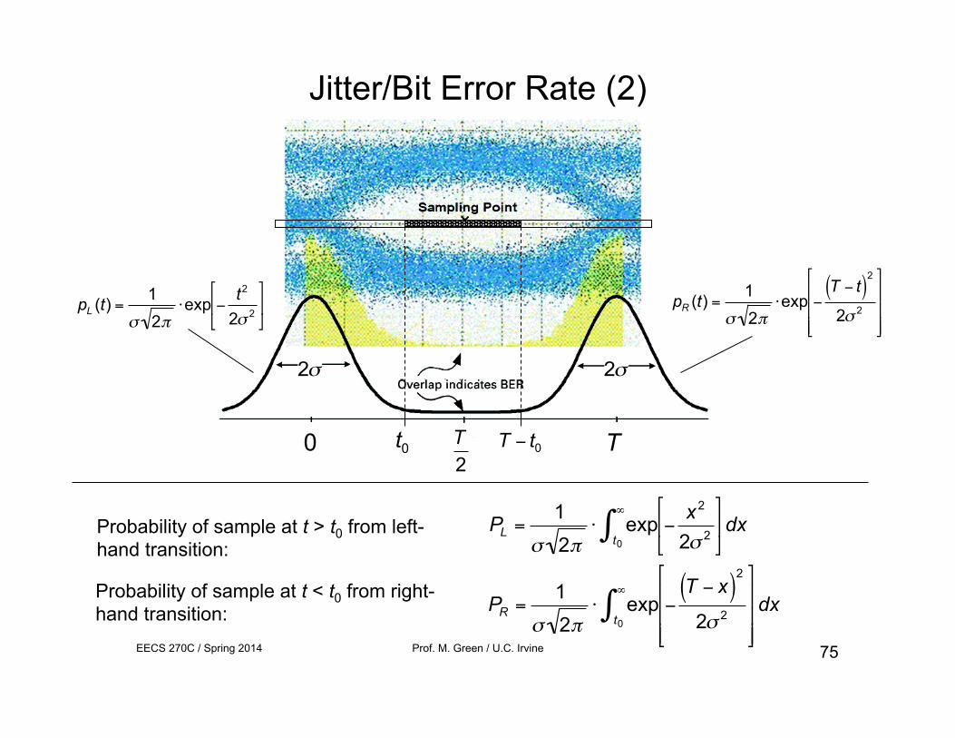
EECS 270C / Spring 2014 Prof. M. Green / U.C. Irvine 75
R
€
2σ
0 T
€
T2
€
t0
€
T − t0
€
PL =1
σ 2π⋅ exp −
x2
2σ 2
&
' (
)
* +
t0
∞
∫ dx
€
PR =1
σ 2π⋅ exp −
T − x( )2
2σ 2
&
'
( ( (
)
*
+ + +
t0
∞
∫ dx
€
pL (t) =1
σ 2π⋅exp −
t2
2σ 2
&
' (
)
* +
€
pR (t) =1
σ 2π⋅exp −
T − t( )2
2σ 2
&
'
( ( (
)
*
+ + +
Probability of sample at t > t0 from left-hand transition:
Probability of sample at t < t0 from right-hand transition:
€
2σ
Jitter/Bit Error Rate (2)

EECS 270C / Spring 2014 Prof. M. Green / U.C. Irvine 76
Total Bit Error Rate (BER) given by:
€
BER = PL + PU =1
σ 2π⋅ exp −
x2
2σ 2
&
' (
)
* +
t0
∞
∫ dx +1
σ 2π⋅ exp −
x2
2σ 2
&
' (
)
* +
T−t0
∞
∫ dx
€
=12
erfc t02σ
#
$ % %
&
' ( ( + erfc T − t0
2σ
#
$ % %
&
' ( (
*
+ , ,
-
. / /
€
where erfc(t) ≡2
π⋅ exp
t
∞
∫ −x2( )dx
€
PL =1
σ 2π⋅ exp −
x2
2σ 2
&
' (
)
* +
t0
∞
∫ dx
€
PR =1
σ 2π⋅ exp −
T − x( )2
2σ 2
&
'
( ( (
)
*
+ + +
t0
∞
∫ dx =1
σ 2π⋅ exp −
x2
2σ 2
&
' (
)
* +
T−t0
∞
∫
Jitter/Bit Error Rate (3)

EECS 270C / Spring 2014 Prof. M. Green / U.C. Irvine 77
€
•
€
•
€
•
€
•
t0 (ps)
log BER
€
σ = 5 ps
€
σ = 2.5 ps
€
σ = 2.5 ps :
€
BER ≤10−12 for t0 ∈ 18ps, 82ps[ ]
€
σ = 5 ps :
€
BER ≤10−12 for t0 ∈ 36ps, 74ps[ ]
Example: T = 100ps
(64 ps eye opening)
(38 ps eye opening)
log(0.5)
Jitter/Bit Error Rate (4)
EECS 270C / Spring 2014 Prof. M. Green / U.C. Irvine 78
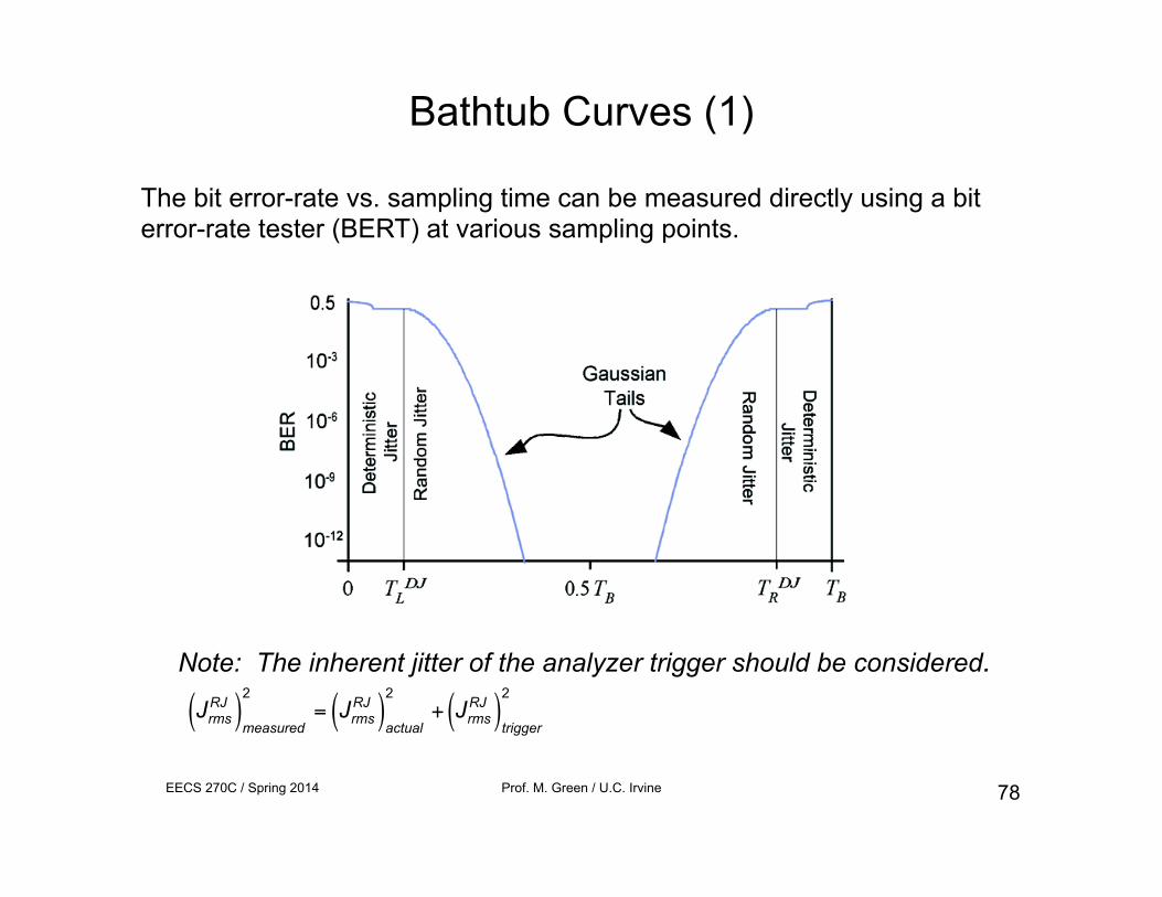
Bathtub Curves (1)
The bit error-rate vs. sampling time can be measured directly using a bit error-rate tester (BERT) at various sampling points.
Note: The inherent jitter of the analyzer trigger should be considered.
€
JrmsRJ( )
measured
2= Jrms
RJ( )actual
2+ Jrms
RJ( )trigger
2

EECS 270C / Spring 2014 Prof. M. Green / U.C. Irvine 79
Bathtub Curves (2)
Bathtub curve can easily be numerically extrapolated to very low BERs (corresponding to random jitter), allowing much lower measurement times.
Example: 10-12 BER with T = 100ps is equivalent to an average of 1 error per 100s. To verify this over a sample of 100 errors would require almost 3 hours!
€
•
€
•
€
•
€
•
t0 (ps)

EECS 270C / Spring 2014 Prof. M. Green / U.C. Irvine 80
Equivalent Peak-to-Peak Total Jitter
BER
10-10
10-11
10-12
10-13
10-14
€
JPPRJ
σ, T determine BER BER determines effective Total jitter given by:
€
JPPRJ
€
JTJ = n ⋅σ( ) + JPPDJ
€
12
nσ
€
p(t)
€
12
nσ
Areas sum to BER
€
12.7 ⋅σ
€
13.4 ⋅σ
€
14.1⋅σ
€
14.7 ⋅σ
€
15.3 ⋅σ


![RF Module Design - [Chapter 7] Voltage-Controlled Oscillator](https://img.dokumen.tips/doc/110x75/55cebbaebb61eb912f8b45f9/rf-module-design-chapter-7-voltage-controlled-oscillator.jpg)


