Embed Size (px)
Citation preview

Vivado Design Suite Tutorial
Power Analysis and Optimization
UG997 (v2014.3) October 1, 2014
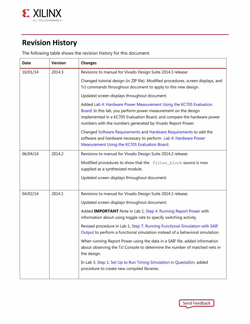
Revision History The following table shows the revision history for this document.
Date Version Changes
10/01/14 2014.3 Revisions to manual for Vivado Design Suite 2014.3 release:
Changed tutorial design (in ZIP file). Modified procedures, screen displays, and Tcl commands throughout document to apply to this new design.
Updated screen displays throughout document.
Added Lab 4: Hardware Power Measurement Using the KC705 Evaluation Board. In this lab, you perform power measurement on the design implemented in a KC705 Evaluation Board, and compare the hardware power numbers with the numbers generated by Vivado Report Power.
Changed Software Requirements and Hardware Requirements to add the software and hardware necessary to perform Lab 4: Hardware Power Measurement Using the KC705 Evaluation Board.
06/04/14 2014.2 Revisions to manual for Vivado Design Suite 2014.2 release:
Modified procedures to show that the filter_block source is now supplied as a synthesized module.
Updated screen displays throughout document.
04/02/14 2014.1 Revisions to manual for Vivado Design Suite 2014.1 release:
Updated screen displays throughout document.
Added IMPORTANT Note in Lab 1, Step 4: Running Report Power with information about using toggle rate to specify switching activity.
Revised procedure in Lab 1, Step 7: Running Functional Simulation with SAIF Output to perform a functional simulation instead of a behavioral simulation.
When running Report Power using the data in a SAIF file, added information about observing the Tcl Console to determine the number of matched nets in the design.
In Lab 3, Step 1: Set Up to Run Timing Simulation in QuestaSim, added procedure to create new compiled libraries.
Send Feedback
Power Analysis and Optimization www.xilinx.com 3 UG997 (v2014.3) October 1, 2014
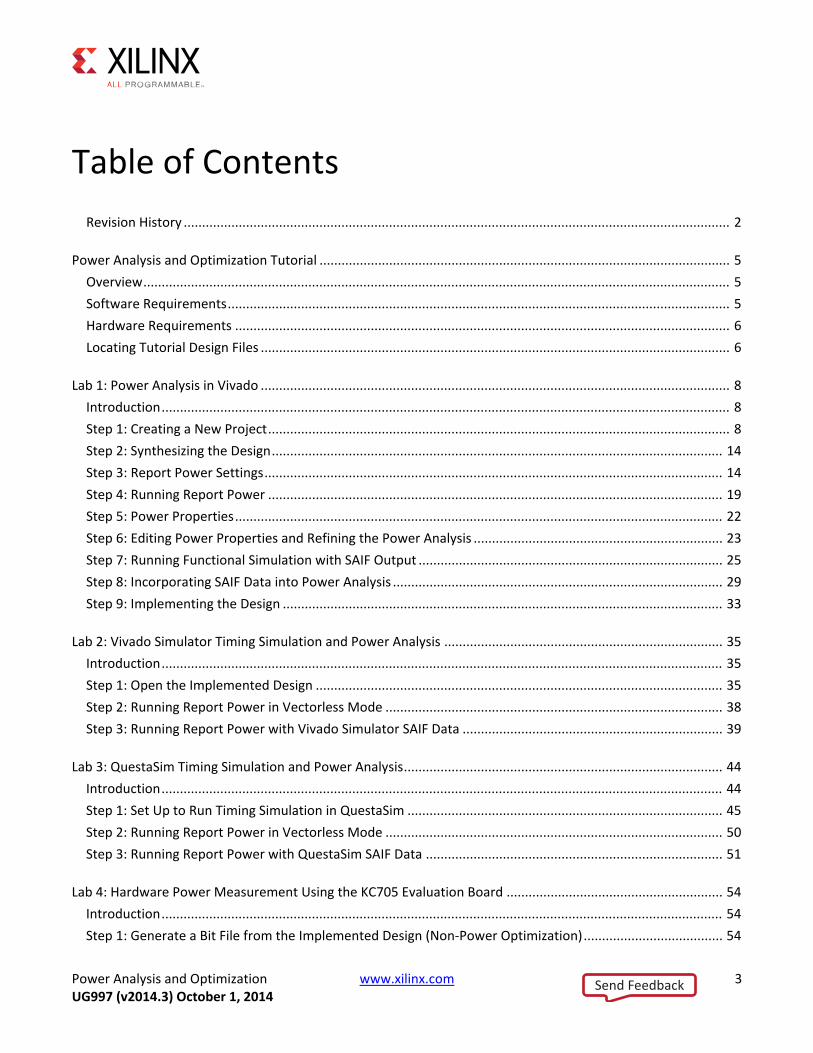
Table of Contents Revision History ..................................................................................................................................................... 2
Power Analysis and Optimization Tutorial ................................................................................................................ 5 Overview ................................................................................................................................................................ 5 Software Requirements ......................................................................................................................................... 5 Hardware Requirements ....................................................................................................................................... 6 Locating Tutorial Design Files ................................................................................................................................ 6
Lab 1: Power Analysis in Vivado ................................................................................................................................ 8 Introduction ........................................................................................................................................................... 8 Step 1: Creating a New Project .............................................................................................................................. 8 Step 2: Synthesizing the Design ........................................................................................................................... 14 Step 3: Report Power Settings ............................................................................................................................. 14 Step 4: Running Report Power ............................................................................................................................ 19 Step 5: Power Properties ..................................................................................................................................... 22 Step 6: Editing Power Properties and Refining the Power Analysis .................................................................... 23 Step 7: Running Functional Simulation with SAIF Output ................................................................................... 25 Step 8: Incorporating SAIF Data into Power Analysis .......................................................................................... 29 Step 9: Implementing the Design ........................................................................................................................ 33
Lab 2: Vivado Simulator Timing Simulation and Power Analysis ............................................................................ 35 Introduction ......................................................................................................................................................... 35 Step 1: Open the Implemented Design ............................................................................................................... 35 Step 2: Running Report Power in Vectorless Mode ............................................................................................ 38 Step 3: Running Report Power with Vivado Simulator SAIF Data ....................................................................... 39
Lab 3: QuestaSim Timing Simulation and Power Analysis ....................................................................................... 44 Introduction ......................................................................................................................................................... 44 Step 1: Set Up to Run Timing Simulation in QuestaSim ...................................................................................... 45 Step 2: Running Report Power in Vectorless Mode ............................................................................................ 50 Step 3: Running Report Power with QuestaSim SAIF Data ................................................................................. 51
Lab 4: Hardware Power Measurement Using the KC705 Evaluation Board ........................................................... 54 Introduction ......................................................................................................................................................... 54 Step 1: Generate a Bit File from the Implemented Design (Non-Power Optimization) ...................................... 54
Send Feedback
Power Analysis and Optimization www.xilinx.com 4 UG997 (v2014.3) October 1, 2014
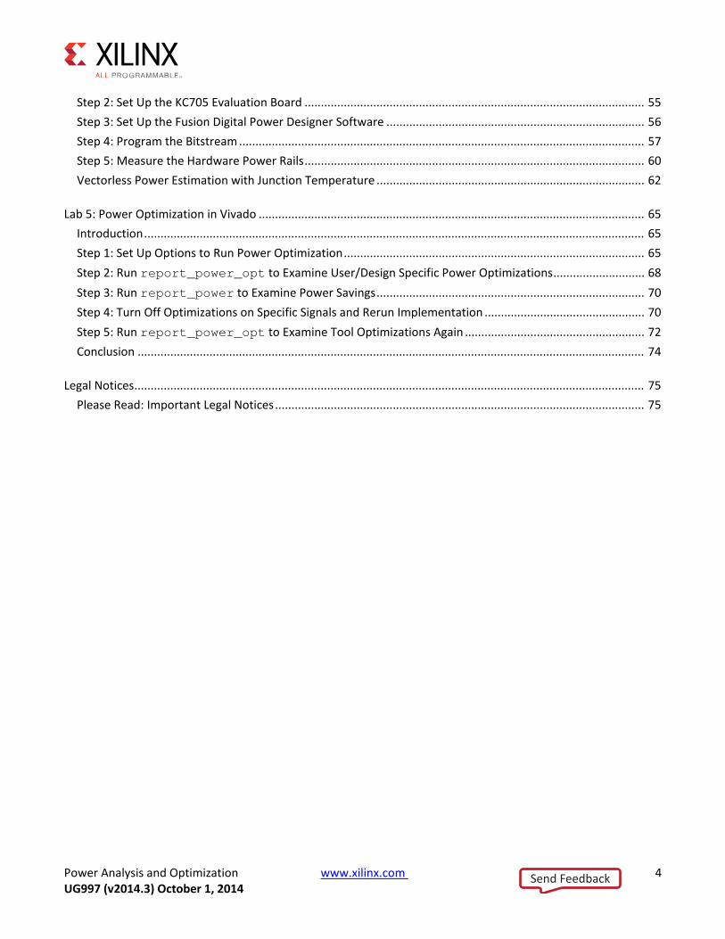
Step 2: Set Up the KC705 Evaluation Board ........................................................................................................ 55 Step 3: Set Up the Fusion Digital Power Designer Software ............................................................................... 56 Step 4: Program the Bitstream ............................................................................................................................ 57 Step 5: Measure the Hardware Power Rails ........................................................................................................ 60 Vectorless Power Estimation with Junction Temperature .................................................................................. 62
Lab 5: Power Optimization in Vivado ...................................................................................................................... 65 Introduction ......................................................................................................................................................... 65 Step 1: Set Up Options to Run Power Optimization ............................................................................................ 65 Step 2: Run report_power_opt to Examine User/Design Specific Power Optimizations ............................ 68 Step 3: Run report_power to Examine Power Savings .................................................................................. 70 Step 4: Turn Off Optimizations on Specific Signals and Rerun Implementation ................................................. 70 Step 5: Run report_power_opt to Examine Tool Optimizations Again ....................................................... 72 Conclusion ........................................................................................................................................................... 74
Legal Notices ............................................................................................................................................................ 75 Please Read: Important Legal Notices ................................................................................................................. 75
Send Feedback
Power Analysis and Optimization www.xilinx.com 5 UG997 (v2014.3) October 1, 2014
Power Analysis and Optimization Tutorial
Overview This tutorial introduces the power analysis and optimization use model recommended for use with the Xilinx® Vivado® Integrated Design Environment (IDE). The tutorial describes the basic steps involved in taking a small example design from RTL to implementation, estimating power through the different stages, and using simulation data to enhance the accuracy of the power analysis. It also describes the steps involved in using the power optimization tools in the design.
VIDEO: The Vivado Design Suite QuickTake Video Tutorial: Power Estimation and Analysis Using Vivado shows how Vivado can help you to estimate power consumption in your design and reviews best practices for getting the most accurate estimation.
VIDEO: The Vivado Design Suite QuickTake Video Tutorial: Power Optimization Using Vivado describes the factors that affect power consumption in an FPGA device and how Vivado helps to minimize power consumption in your design, and looks at some advanced control and best practices for getting the most out of Vivado power optimization.
Software Requirements This tutorial requires that the 2014.3 Vivado Design Suite software release or later is installed. For installation instructions and information, see the Vivado Design Suite User Guide: Release Notes, Installation, and Licensing (UG973).
For Hardware Power Measurement, the tutorial requires Texas Instruments Fusion Digital Power Designer software, which can be downloaded from this location:
www.ti.com/tool/fusion_digital_power_designer
Send Feedback
Power Analysis and Optimization Tutorial
Power Analysis and Optimization www.xilinx.com 6 UG997 (v2014.3) October 1, 2014
Hardware Requirements Hardware requirements for this Tutorial are:
• Supported Operating Systems to run the Vivado Design Suite, and memory recommendations when using the Vivado tools, are described in the Vivado Design Suite User Guide: Release Notes, Installation, and Licensing (UG973).
• The hardware power measurements in Lab 4: Hardware Power Measurement Using the KC705 Evaluation Board require a Xilinx Kintex-7 FPGA KC705 Evaluation Kit. You can find information on the Evaluation Kit at this location:
www.xilinx.com/products/boards-and-kits/EK-K7-KC705-G.htm
• For power measurements through TI Power Regulators (needed in Lab 4: Hardware Power Measurement Using the KC705 Evaluation Board), use the Texas Instruments USB Interface Adapter. You can find information on the USB Interface Adaptor at this location:
www.ti.com/lit/ml/sllu093/sllu093.pdf.
Locating Tutorial Design Files 1. Download the ug997-vivado-power-analysis-optimization-tutorial.zip file from
the Xilinx website:
https://secure.xilinx.com/webreg/clickthrough.do?cid=363353&license= RefDesLicense&filename=ug997-vivado-power-analysis-optimization-tutorial.zip
2. Extract the zip file contents into any write-accessible location.
This tutorial refers to the location of the extracted ug997-vivado-power-analysis-optimization-tutorial.zip file contents as <Extract_Dir>.
IMPORTANT: You will modify the tutorial design data while working through this tutorial. Use a new copy of the original data each time you start this tutorial.
Send Feedback
Power Analysis and Optimization Tutorial
Power Analysis and Optimization www.xilinx.com 7 UG997 (v2014.3) October 1, 2014
The following table describes the contents of the zip file containing the tutorial design files, ug997-vivado-power-analysis-optimization-tutorial.zip.
Directories/Files Description
/src Contains the design HDL and testbench for the functional simulation.
/src/dut_fpga.v Top module for the design.
/src/bram_tdp.v /src/bram_top.v /src/dut.v
Other design blocks - synthesized module.
dut_fpga_kc705.xdc Contains clocking and timing constraints for the design.
/src/testbench.v Testbench for simulating the design.
readme.txt A readme file about the tutorial design.
Send Feedback

Power Analysis and Optimization www.xilinx.com 8 UG997 (v2014.3) October 1, 2014
Lab 1: Power Analysis in Vivado
Introduction In this lab, you will learn about the Power Analysis and Optimization features in the Vivado IDE. The lab will take you through the steps of project creation and power analysis at the synthesis stage, using the Vivado Report Power feature in vectorless mode. It will also demonstrate using the SAIF file generated from behavioral simulation for Vivado Report Power Analysis.
You will analyze power in the Vivado IDE. Then you will examine some of the major features in the Power Report window and closely examine some power specific Tcl commands. You will also learn to create a SAIF file by simulating the design in the timing simulation stage using both the Vivado simulator and QuestaSim.
You will also learn how to invoke Power Optimization after opt_design in the Vivado IDE. You will examine the power optimization report and selectively turn power optimizations ON or OFF on specific signals, nets, modules, or hierarchy.
Step 1: Creating a New Project To create a project, use the New Project wizard to name the project, to add RTL source files and constraints, and to specify the target device.
• On Linux,
1. Go to the directory where the lab materials are stored:
cd <Extract_Dir>/Vivado_Power_Tutorial
2. Launch the Vivado IDE: vivado
Send Feedback
Lab 1: Power Analysis in Vivado
Power Analysis and Optimization www.xilinx.com 9 UG997 (v2014.3) October 1, 2014
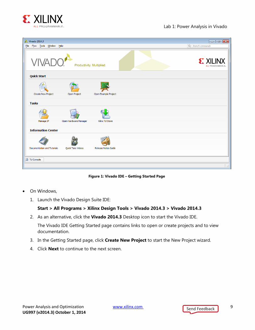
Figure 1: Vivado IDE – Getting Started Page
• On Windows,
1. Launch the Vivado Design Suite IDE:
Start > All Programs > Xilinx Design Tools > Vivado 2014.3 > Vivado 2014.3
2. As an alternative, click the Vivado 2014.3 Desktop icon to start the Vivado IDE.
The Vivado IDE Getting Started page contains links to open or create projects and to view documentation.
3. In the Getting Started page, click Create New Project to start the New Project wizard.
4. Click Next to continue to the next screen.
Send Feedback
Lab 1: Power Analysis in Vivado
Power Analysis and Optimization www.xilinx.com 10 UG997 (v2014.3) October 1, 2014
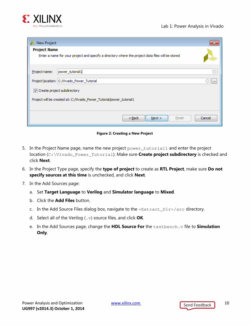
Figure 2: Creating a New Project
5. In the Project Name page, name the new project power_tutorial1 and enter the project location (C:\Vivado_Power_Tutorial). Make sure Create project subdirectory is checked and click Next.
6. In the Project Type page, specify the type of project to create as RTL Project, make sure Do not specify sources at this time is unchecked, and click Next.
7. In the Add Sources page:
a. Set Target Language to Verilog and Simulator language to Mixed.
b. Click the Add Files button.
c. In the Add Source Files dialog box, navigate to the <Extract_Dir>/src directory.
d. Select all of the Verilog (.v) source files, and click OK.
e. In the Add Sources page, change the HDL Source For the testbench.v file to Simulation Only.
Send Feedback
Lab 1: Power Analysis in Vivado
Power Analysis and Optimization www.xilinx.com 11 UG997 (v2014.3) October 1, 2014
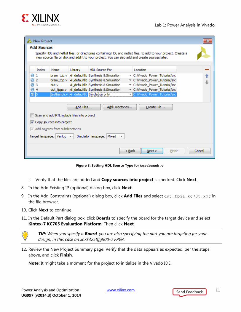
Figure 3: Setting HDL Source Type for testbench.v
f. Verify that the files are added and Copy sources into project is checked. Click Next.
8. In the Add Existing IP (optional) dialog box, click Next.
9. In the Add Constraints (optional) dialog box, click Add Files and select dut_fpga_kc705.xdc in the file browser.
10. Click Next to continue.
11. In the Default Part dialog box, click Boards to specify the board for the target device and select Kintex-7 KC705 Evaluation Platform. Then click Next.
TIP: When you specify a Board, you are also specifying the part you are targeting for your design, in this case an xc7k325tffg900-2 FPGA.
12. Review the New Project Summary page. Verify that the data appears as expected, per the steps above, and click Finish.
Note: It might take a moment for the project to initialize in the Vivado IDE.
Send Feedback
Lab 1: Power Analysis in Vivado
Power Analysis and Optimization www.xilinx.com 12 UG997 (v2014.3) October 1, 2014
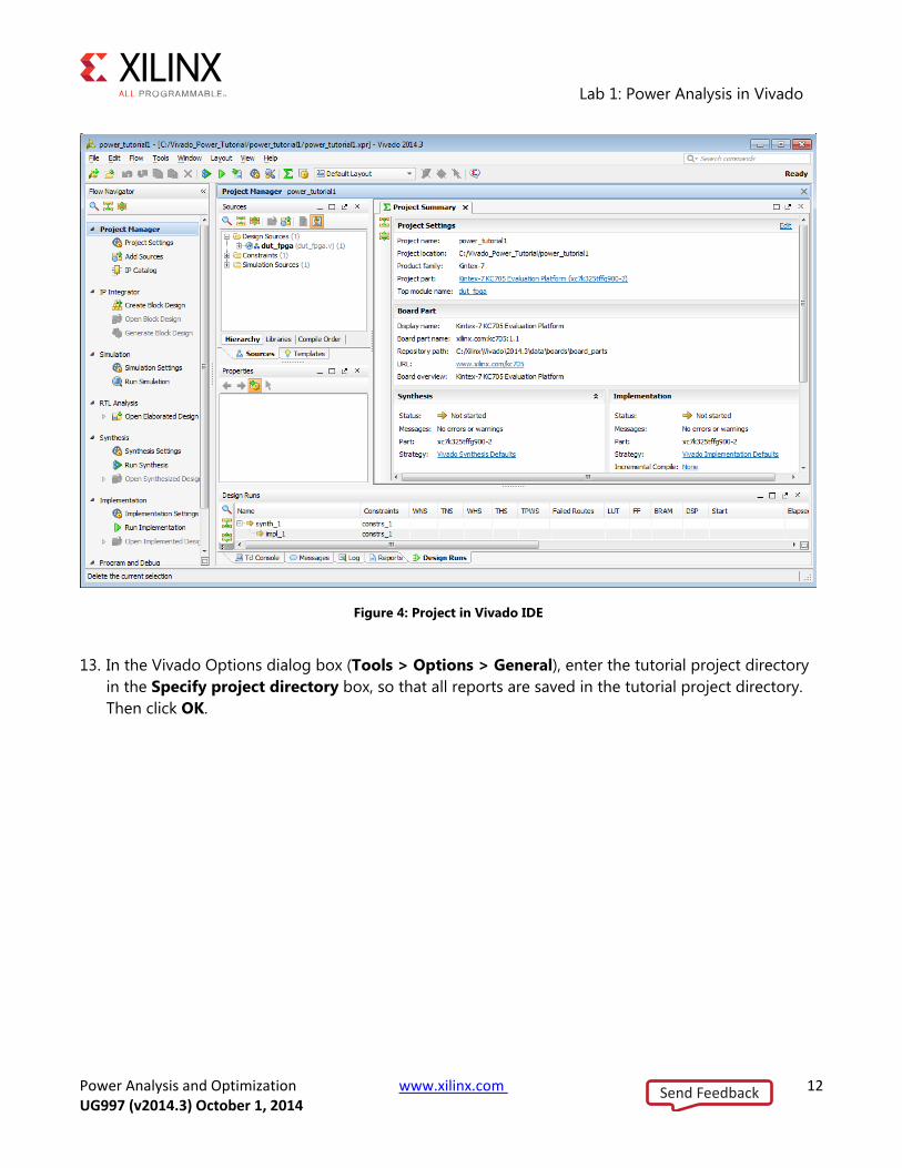
Figure 4: Project in Vivado IDE
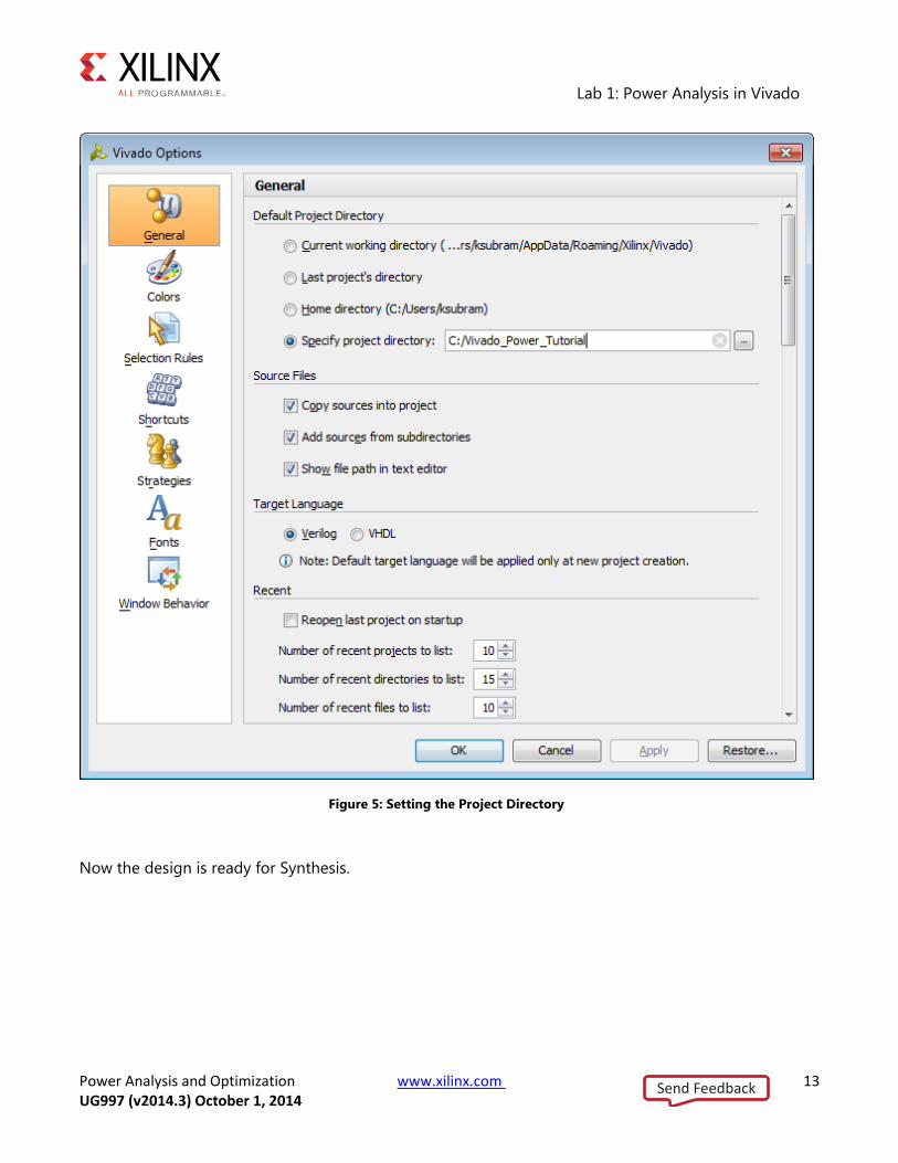
13. In the Vivado Options dialog box (Tools > Options > General), enter the tutorial project directory in the Specify project directory box, so that all reports are saved in the tutorial project directory. Then click OK.
Send Feedback
Lab 1: Power Analysis in Vivado
Power Analysis and Optimization www.xilinx.com 13 UG997 (v2014.3) October 1, 2014
Figure 5: Setting the Project Directory
Now the design is ready for Synthesis.
Send Feedback
Lab 1: Power Analysis in Vivado
Power Analysis and Optimization www.xilinx.com 14 UG997 (v2014.3) October 1, 2014
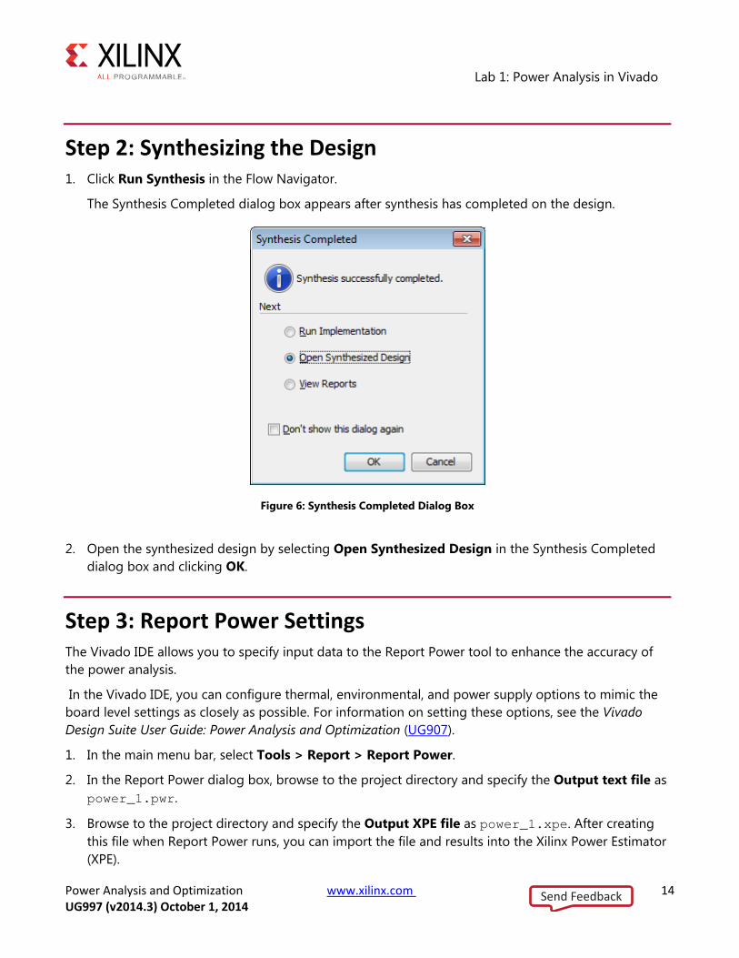
Step 2: Synthesizing the Design 1. Click Run Synthesis in the Flow Navigator.
The Synthesis Completed dialog box appears after synthesis has completed on the design.
Figure 6: Synthesis Completed Dialog Box
2. Open the synthesized design by selecting Open Synthesized Design in the Synthesis Completed dialog box and clicking OK.
Step 3: Report Power Settings The Vivado IDE allows you to specify input data to the Report Power tool to enhance the accuracy of the power analysis.
In the Vivado IDE, you can configure thermal, environmental, and power supply options to mimic the board level settings as closely as possible. For information on setting these options, see the Vivado Design Suite User Guide: Power Analysis and Optimization (UG907).
1. In the main menu bar, select Tools > Report > Report Power.
2. In the Report Power dialog box, browse to the project directory and specify the Output text file as power_1.pwr.
3. Browse to the project directory and specify the Output XPE file as power_1.xpe. After creating this file when Report Power runs, you can import the file and results into the Xilinx Power Estimator (XPE).
Send Feedback
Lab 1: Power Analysis in Vivado
Power Analysis and Optimization www.xilinx.com 15 UG997 (v2014.3) October 1, 2014
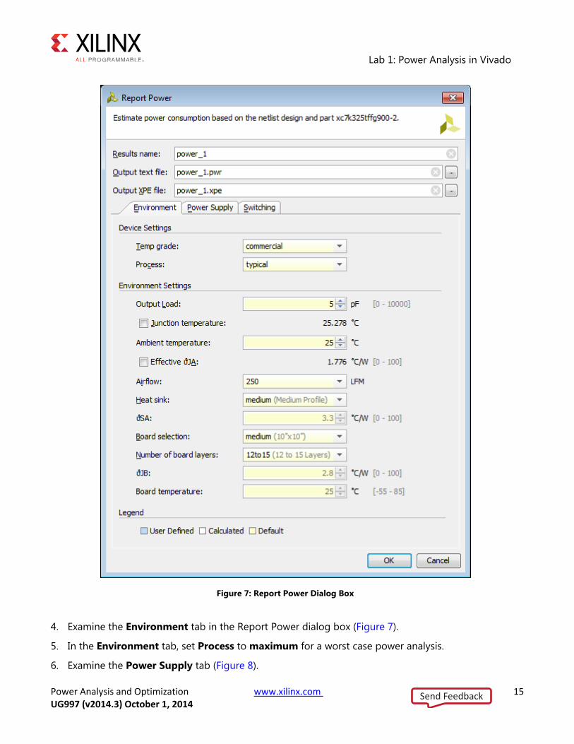
Figure 7: Report Power Dialog Box
4. Examine the Environment tab in the Report Power dialog box (Figure 7).
5. In the Environment tab, set Process to maximum for a worst case power analysis.
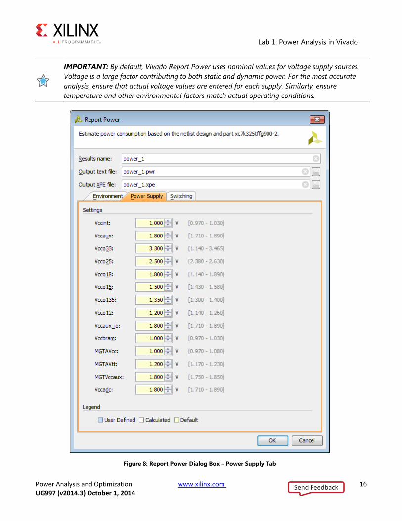
6. Examine the Power Supply tab (Figure 8).
Send Feedback
Lab 1: Power Analysis in Vivado
Power Analysis and Optimization www.xilinx.com 16 UG997 (v2014.3) October 1, 2014
IMPORTANT: By default, Vivado Report Power uses nominal values for voltage supply sources. Voltage is a large factor contributing to both static and dynamic power. For the most accurate analysis, ensure that actual voltage values are entered for each supply. Similarly, ensure temperature and other environmental factors match actual operating conditions.
Figure 8: Report Power Dialog Box – Power Supply Tab
Send Feedback

Lab 1: Power Analysis in Vivado
Power Analysis and Optimization www.xilinx.com 17 UG997 (v2014.3) October 1, 2014
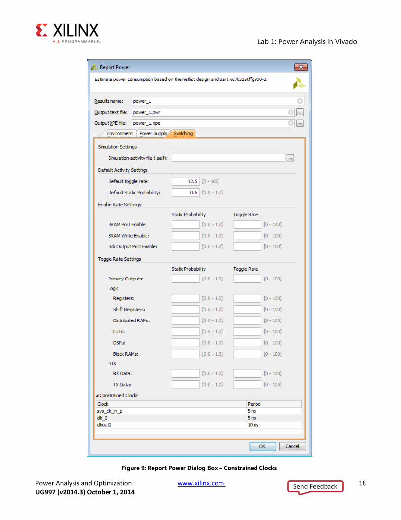
7. In the Switching tab, click on Constrained Clocks and examine the constrained clocks in the design.
IMPORTANT: Make sure all the relevant clocks in the design are constrained. All the design clocks must be defined using create_clock or create_generated_clock' XDC constraints, so that Report Power recognizes the clocks. Default toggle rate is set to 12.5% and Default percent high is set to 0.5. This will be applied to primary ports (non-clock) and block box outputs.
Send Feedback
Lab 1: Power Analysis in Vivado
Power Analysis and Optimization www.xilinx.com 18 UG997 (v2014.3) October 1, 2014
Figure 9: Report Power Dialog Box – Constrained Clocks
Send Feedback
Lab 1: Power Analysis in Vivado
Power Analysis and Optimization www.xilinx.com 19 UG997 (v2014.3) October 1, 2014
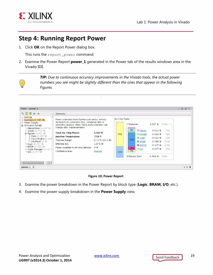
Step 4: Running Report Power 1. Click OK on the Report Power dialog box.
This runs the report_power command.
2. Examine the Power Report power_1 generated in the Power tab of the results windows area in the Vivado IDE.
TIP: Due to continuous accuracy improvements in the Vivado tools, the actual power numbers you see might be slightly different than the ones that appear in the following Figures.
Figure 10: Power Report
3. Examine the power breakdown in the Power Report by block type (Logic, BRAM, I/O, etc.).
4. Examine the power supply breakdown in the Power Supply view.
Send Feedback
Lab 1: Power Analysis in Vivado
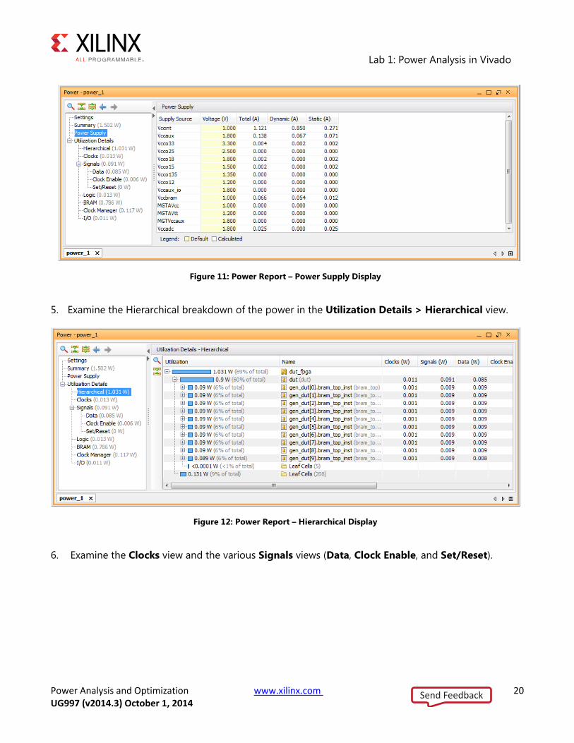
Power Analysis and Optimization www.xilinx.com 20 UG997 (v2014.3) October 1, 2014
Figure 11: Power Report – Power Supply Display
5. Examine the Hierarchical breakdown of the power in the Utilization Details > Hierarchical view.
Figure 12: Power Report – Hierarchical Display
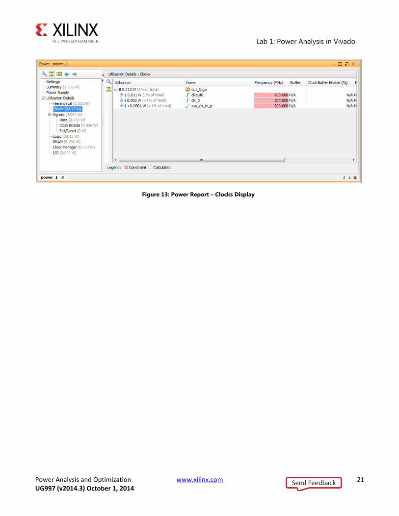
6. Examine the Clocks view and the various Signals views (Data, Clock Enable, and Set/Reset).
Send Feedback
Lab 1: Power Analysis in Vivado
Power Analysis and Optimization www.xilinx.com 21 UG997 (v2014.3) October 1, 2014
Figure 13: Power Report – Clocks Display
Send Feedback
Lab 1: Power Analysis in Vivado
Power Analysis and Optimization www.xilinx.com 22 UG997 (v2014.3) October 1, 2014
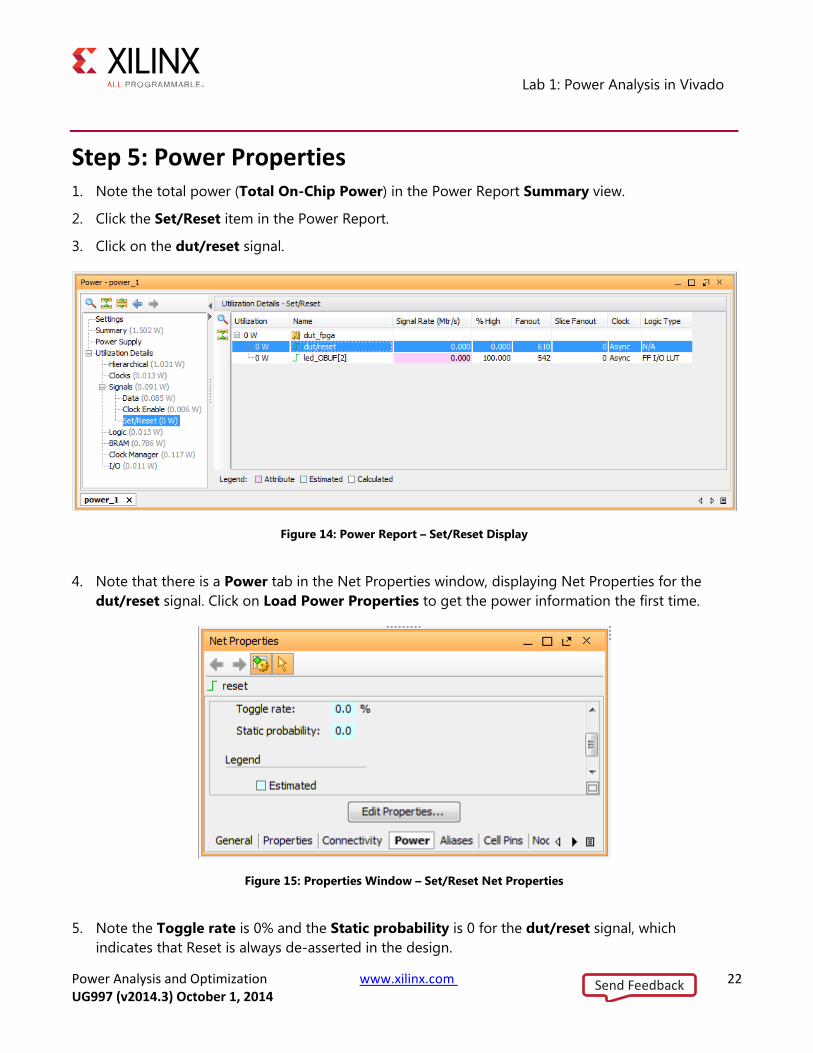
Step 5: Power Properties 1. Note the total power (Total On-Chip Power) in the Power Report Summary view.
2. Click the Set/Reset item in the Power Report.
3. Click on the dut/reset signal.
Figure 14: Power Report – Set/Reset Display
4. Note that there is a Power tab in the Net Properties window, displaying Net Properties for the dut/reset signal. Click on Load Power Properties to get the power information the first time.
Figure 15: Properties Window – Set/Reset Net Properties
5. Note the Toggle rate is 0% and the Static probability is 0 for the dut/reset signal, which indicates that Reset is always de-asserted in the design.
Send Feedback
Lab 1: Power Analysis in Vivado
Power Analysis and Optimization www.xilinx.com 23 UG997 (v2014.3) October 1, 2014
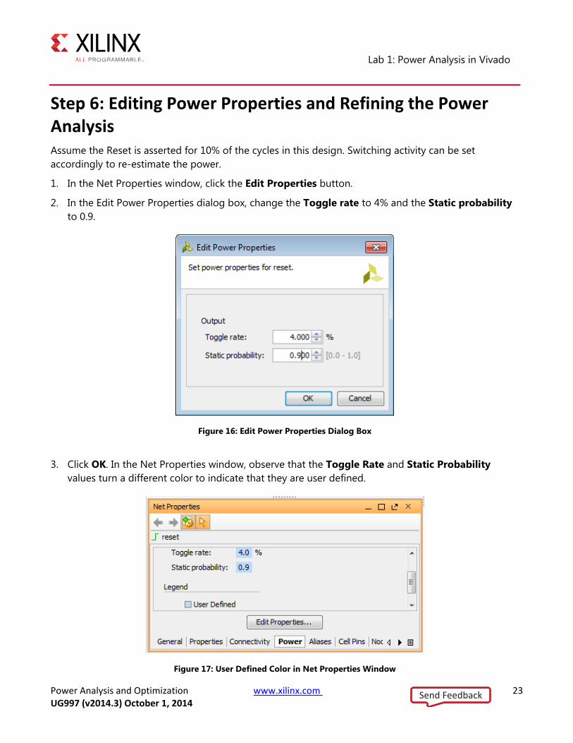
Step 6: Editing Power Properties and Refining the Power Analysis Assume the Reset is asserted for 10% of the cycles in this design. Switching activity can be set accordingly to re-estimate the power.
1. In the Net Properties window, click the Edit Properties button.
2. In the Edit Power Properties dialog box, change the Toggle rate to 4% and the Static probability to 0.9.
Figure 16: Edit Power Properties Dialog Box
3. Click OK. In the Net Properties window, observe that the Toggle Rate and Static Probability values turn a different color to indicate that they are user defined.
Figure 17: User Defined Color in Net Properties Window
Send Feedback
Lab 1: Power Analysis in Vivado
Power Analysis and Optimization www.xilinx.com 24 UG997 (v2014.3) October 1, 2014
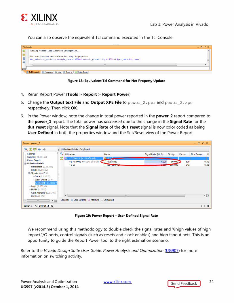
You can also observe the equivalent Tcl command executed in the Tcl Console.
Figure 18: Equivalent Tcl Command for Net Property Update
4. Rerun Report Power (Tools > Report > Report Power).
5. Change the Output text File and Output XPE File to power_2.pwr and power_2.xpe respectively. Then click OK.
6. In the Power window, note the change in total power reported in the power_2 report compared to the power_1 report. The total power has decreased due to the change in the Signal Rate for the dut_reset signal. Note that the Signal Rate of the dut_reset signal is now color coded as being User Defined in both the properties window and the Set/Reset view of the Power Report.
Figure 19: Power Report – User Defined Signal Rate
We recommend using this methodology to double check the signal rates and %high values of high impact I/O ports, control signals (such as resets and clock enables) and high fanout nets. This is an opportunity to guide the Report Power tool to the right estimation scenario.
Refer to the Vivado Design Suite User Guide: Power Analysis and Optimization (UG907) for more information on switching activity.
Send Feedback
Lab 1: Power Analysis in Vivado
Power Analysis and Optimization www.xilinx.com 25 UG997 (v2014.3) October 1, 2014
TIP: In Tcl, use the set_switching_activity command to change the signal rate and static probability of signals and use report_switching_activity to query the values that were set on the signals.
set_switching_activity -signal_rate 4 -static_probability 0.9 [get_nets dut/reset]
report_switching_activity [get_nets dut/reset]
IMPORTANT: Switching activity can also be specified in terms of toggle rate. Toggle rate is always associated with a clock. The primary ports can be associated with a specific clock using the set_input_delay command. For example:
set_input_delay -clock CLK 1 [get_nets dut/reset] If no clock association is found, Report Power will associate the ports with respect to the capturing clock. Now you can set the toggle rate on the reset net:
set_switching_activity -toggle_rate 4 -static_probability 0.9 [get_nets dut/reset]
This is equivalent to a signal rate of 4 MTr/s (signal_rate = toggle_rate * Freq = 4 * 100MHz ).
Step 7: Running Functional Simulation with SAIF Output Now that you have created a Vivado project for the tutorial design, you can set up and launch the Vivado simulator to run post-synthesis functional simulation. Simulation will generate a switching activity values file (SAIF) that will enable you to do more accurate power estimation on your design.
1. In the Flow Navigator, click Simulation Settings to set the behavioral simulation properties.
2. In the Project Settings dialog box, note that the following Simulation defaults are automatically set:
Simulator language: Mixed
Simulation set: sim_1
Simulation top-module name: testbench
Send Feedback
Lab 1: Power Analysis in Vivado
Power Analysis and Optimization www.xilinx.com 26 UG997 (v2014.3) October 1, 2014
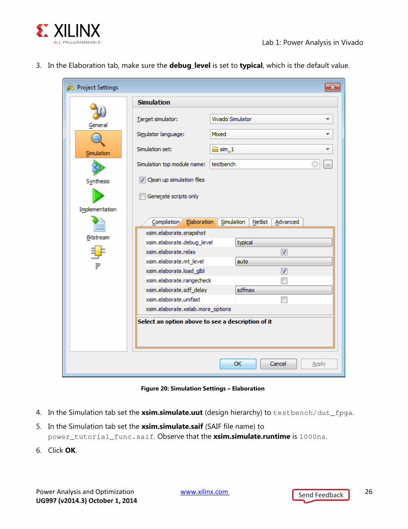
3. In the Elaboration tab, make sure the debug_level is set to typical, which is the default value.
Figure 20: Simulation Settings – Elaboration
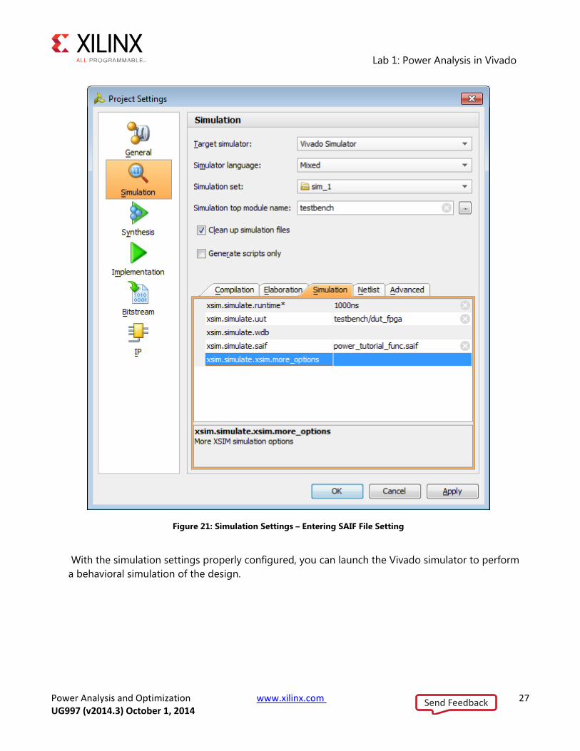
4. In the Simulation tab set the xsim.simulate.uut (design hierarchy) to testbench/dut_fpga.
5. In the Simulation tab set the xsim.simulate.saif (SAIF file name) to power_tutorial_func.saif. Observe that the xsim.simulate.runtime is 1000ns.
6. Click OK.
Send Feedback
Lab 1: Power Analysis in Vivado
Power Analysis and Optimization www.xilinx.com 27 UG997 (v2014.3) October 1, 2014
Figure 21: Simulation Settings – Entering SAIF File Setting
With the simulation settings properly configured, you can launch the Vivado simulator to perform a behavioral simulation of the design.
Send Feedback
Lab 1: Power Analysis in Vivado
Power Analysis and Optimization www.xilinx.com 28 UG997 (v2014.3) October 1, 2014
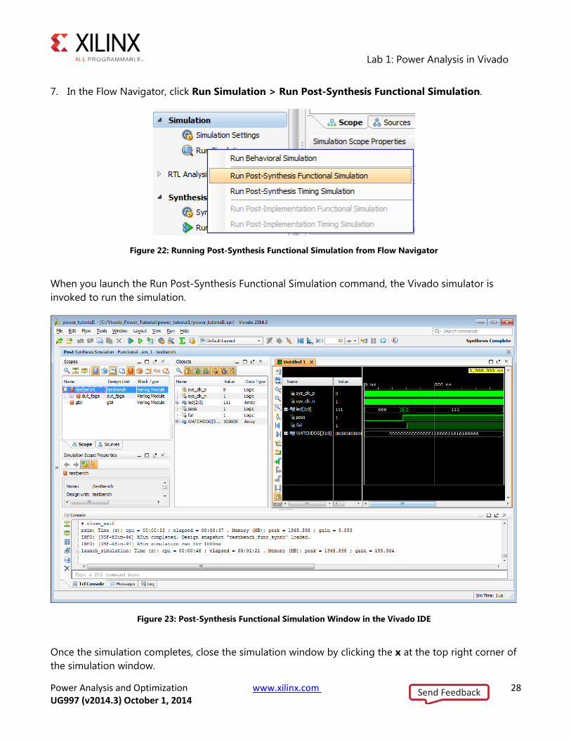
7. In the Flow Navigator, click Run Simulation > Run Post-Synthesis Functional Simulation.
Figure 22: Running Post-Synthesis Functional Simulation from Flow Navigator
When you launch the Run Post-Synthesis Functional Simulation command, the Vivado simulator is invoked to run the simulation.
Figure 23: Post-Synthesis Functional Simulation Window in the Vivado IDE
Once the simulation completes, close the simulation window by clicking the x at the top right corner of the simulation window.
Send Feedback
Lab 1: Power Analysis in Vivado
Power Analysis and Optimization www.xilinx.com 29 UG997 (v2014.3) October 1, 2014
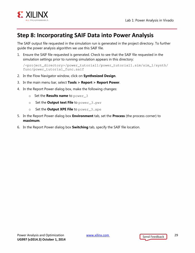
Step 8: Incorporating SAIF Data into Power Analysis The SAIF output file requested in the simulation run is generated in the project directory. To further guide the power analysis algorithm we use this SAIF file.
1. Ensure the SAIF file requested is generated. Check to see that the SAIF file requested in the simulation settings prior to running simulation appears in this directory:
/<project_directory>/power_tutorial1/power_tutorial1.sim/sim_1/synth/ func/power_tutorial_func.saif
2. In the Flow Navigator window, click on Synthesized Design.
3. In the main menu bar, select Tools > Report > Report Power.
4. In the Report Power dialog box, make the following changes:
o Set the Results name to power_3
o Set the Output text File to power_3.pwr
o Set the Output XPE File to power_3.xpe
5. In the Report Power dialog box Environment tab, set the Process (the process corner) to maximum.
6. In the Report Power dialog box Switching tab, specify the SAIF file location.
Send Feedback
Lab 1: Power Analysis in Vivado
Power Analysis and Optimization www.xilinx.com 30 UG997 (v2014.3) October 1, 2014
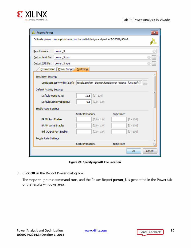
Figure 24: Specifying SAIF File Location
7. Click OK in the Report Power dialog box.
The report_power command runs, and the Power Report power_3 is generated in the Power tab of the results windows area.
Send Feedback
Lab 1: Power Analysis in Vivado
Power Analysis and Optimization www.xilinx.com 31 UG997 (v2014.3) October 1, 2014
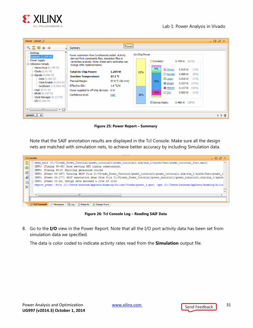
Figure 25: Power Report – Summary
Note that the SAIF annotation results are displayed in the Tcl Console. Make sure all the design nets are matched with simulation nets, to achieve better accuracy by including Simulation data.
Figure 26: Tcl Console Log – Reading SAIF Data
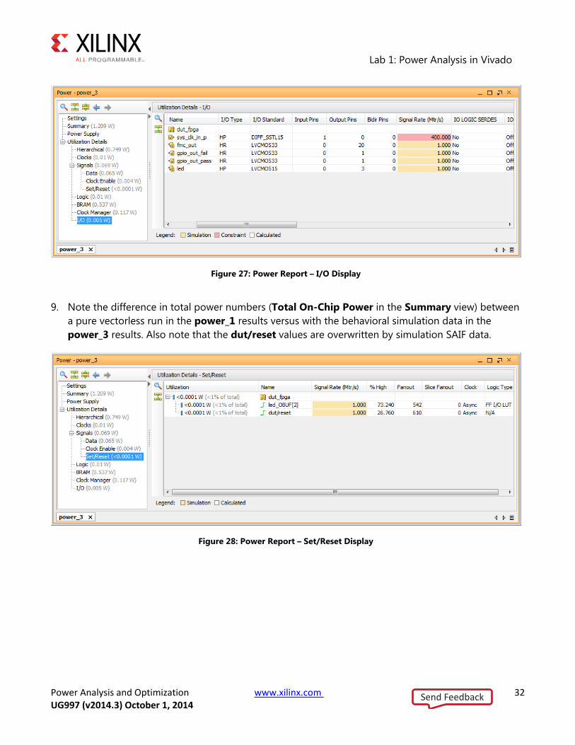
8. Go to the I/O view in the Power Report. Note that all the I/O port activity data has been set from simulation data we specified.
The data is color coded to indicate activity rates read from the Simulation output file.
Send Feedback
Lab 1: Power Analysis in Vivado
Power Analysis and Optimization www.xilinx.com 32 UG997 (v2014.3) October 1, 2014
Figure 27: Power Report – I/O Display
9. Note the difference in total power numbers (Total On-Chip Power in the Summary view) between a pure vectorless run in the power_1 results versus with the behavioral simulation data in the power_3 results. Also note that the dut/reset values are overwritten by simulation SAIF data.
Figure 28: Power Report – Set/Reset Display
Send Feedback
Lab 1: Power Analysis in Vivado
Power Analysis and Optimization www.xilinx.com 33 UG997 (v2014.3) October 1, 2014
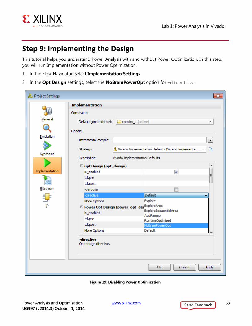
Step 9: Implementing the Design This tutorial helps you understand Power Analysis with and without Power Optimization. In this step, you will run Implementation without Power Optimization.
1. In the Flow Navigator, select Implementation Settings.
2. In the Opt Design settings, select the NoBramPowerOpt option for -directive.
Figure 29: Disabling Power Optimization
Send Feedback
Lab 1: Power Analysis in Vivado
Power Analysis and Optimization www.xilinx.com 34 UG997 (v2014.3) October 1, 2014
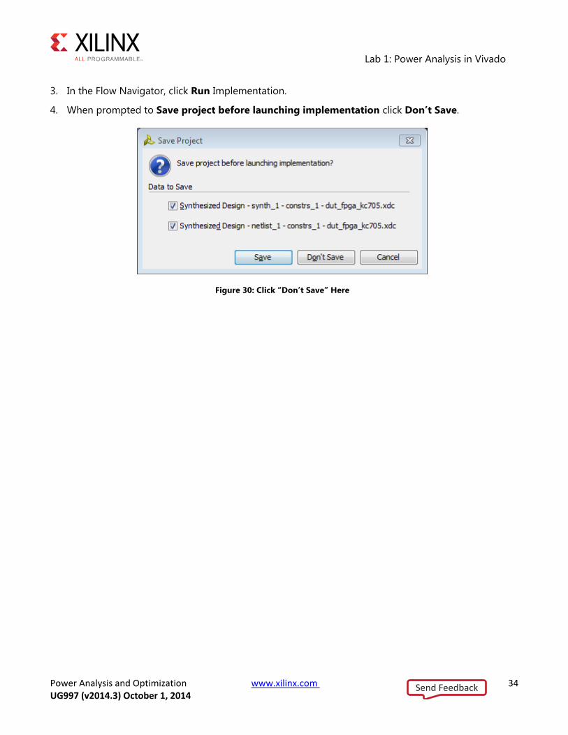
3. In the Flow Navigator, click Run Implementation.
4. When prompted to Save project before launching implementation click Don’t Save.
Figure 30: Click “Don’t Save” Here
Send Feedback
Power Analysis and Optimization www.xilinx.com 35 UG997 (v2014.3) October 1, 2014
Lab 2: Vivado Simulator Timing Simulation and Power Analysis
Introduction In this lab, you will learn about generating a SAIF file after running a timing level simulation using the Vivado Simulator. The lab will take you through the steps for SAIF file creation, running timing simulation, and estimating power using the SAIF data.
Step 1: Open the Implemented Design 1. In the Implementation Complete dialog box, select Open Implemented Design and click OK to
open the implemented design. When prompted to Save project before launching implementation click Don’t Save.
Now you are ready to set up and launch the Vivado simulator to run post implementation timing simulation. You will set the timing simulation properties in the Vivado IDE, then run the timing simulation.
2. In the Flow Navigator, click Simulation Settings to set the timing simulation properties.
3. In the Project Settings dialog box, note that the following defaults are automatically set:
Simulation set: sim_1
Simulation top-module name: testbench
4. In the Elaboration tab, make sure that debug_level is set to typical, which is the default value.
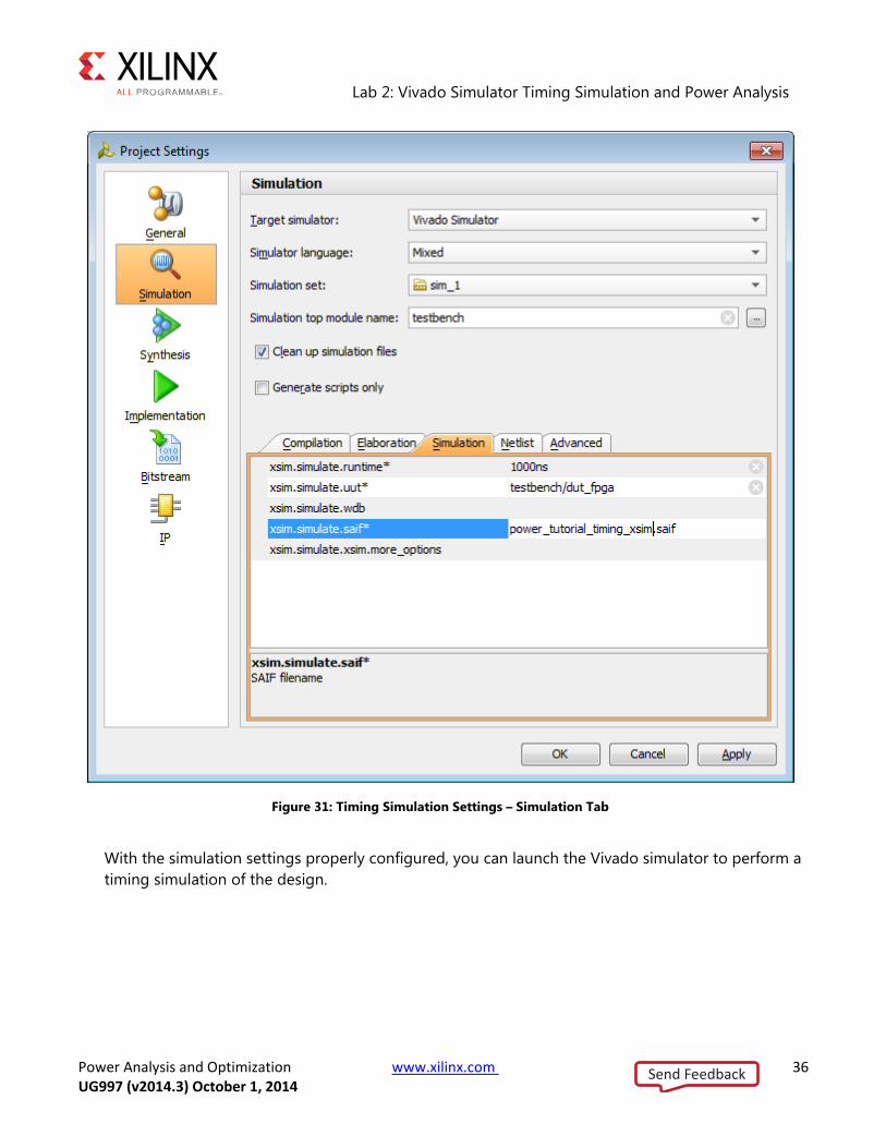
5. In the Simulation tab set the Design Under Test Instance to testbench/dut_fpga and the SAIF Filename to power_tutorial_timing_xsim.saif.
6. Observe that the Simulation Run Time is 1000ns.
7. Click OK.
Send Feedback
Lab 2: Vivado Simulator Timing Simulation and Power Analysis
Power Analysis and Optimization www.xilinx.com 36 UG997 (v2014.3) October 1, 2014
Figure 31: Timing Simulation Settings – Simulation Tab
With the simulation settings properly configured, you can launch the Vivado simulator to perform a timing simulation of the design.
Send Feedback
Lab 2: Vivado Simulator Timing Simulation and Power Analysis
Power Analysis and Optimization www.xilinx.com 37 UG997 (v2014.3) October 1, 2014
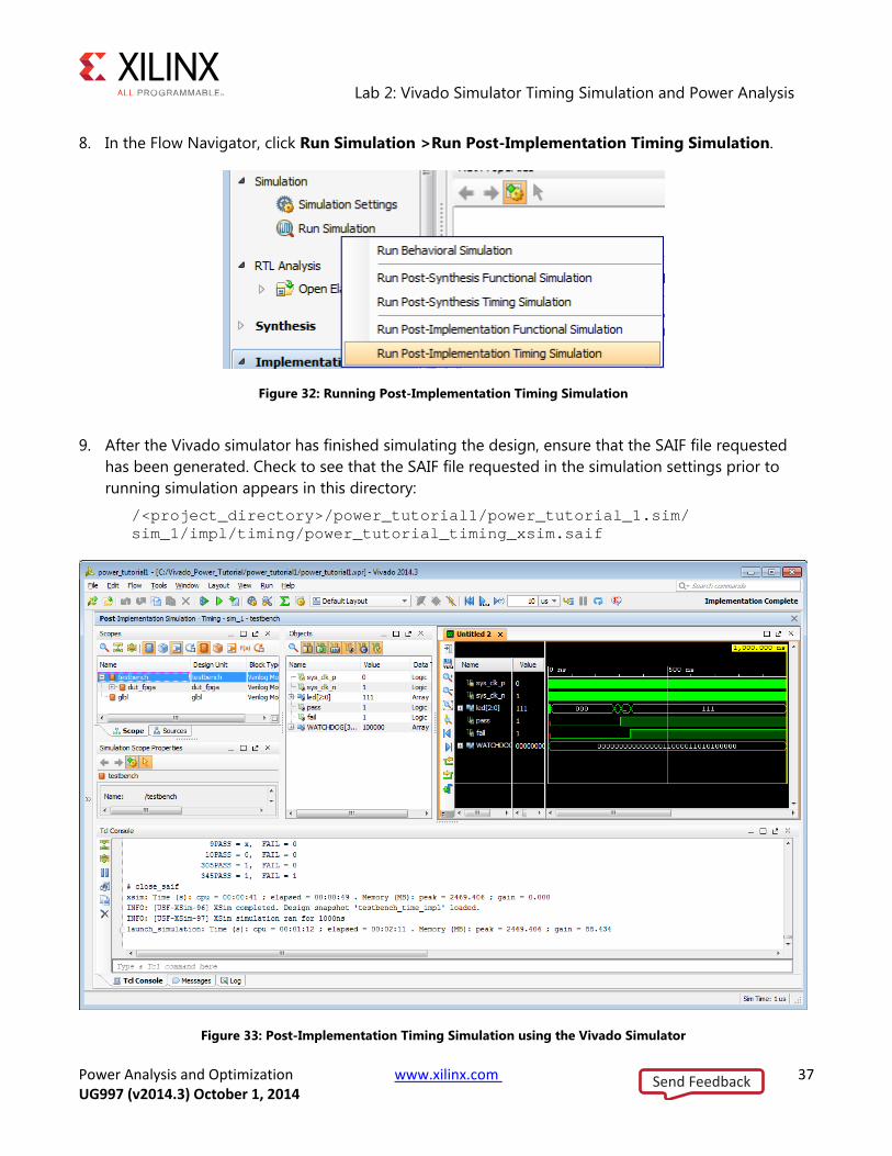
8. In the Flow Navigator, click Run Simulation >Run Post-Implementation Timing Simulation.
Figure 32: Running Post-Implementation Timing Simulation
9. After the Vivado simulator has finished simulating the design, ensure that the SAIF file requested has been generated. Check to see that the SAIF file requested in the simulation settings prior to running simulation appears in this directory:
/<project_directory>/power_tutorial1/power_tutorial_1.sim/ sim_1/impl/timing/power_tutorial_timing_xsim.saif
Figure 33: Post-Implementation Timing Simulation using the Vivado Simulator
Send Feedback
Lab 2: Vivado Simulator Timing Simulation and Power Analysis
Power Analysis and Optimization www.xilinx.com 38 UG997 (v2014.3) October 1, 2014
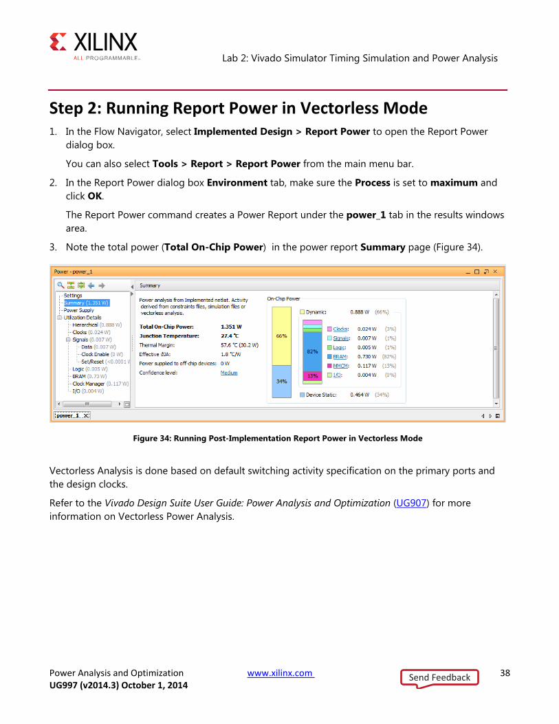
Step 2: Running Report Power in Vectorless Mode 1. In the Flow Navigator, select Implemented Design > Report Power to open the Report Power
dialog box.
You can also select Tools > Report > Report Power from the main menu bar.
2. In the Report Power dialog box Environment tab, make sure the Process is set to maximum and click OK.
The Report Power command creates a Power Report under the power_1 tab in the results windows area.
3. Note the total power (Total On-Chip Power) in the power report Summary page (Figure 34).
Figure 34: Running Post-Implementation Report Power in Vectorless Mode
Vectorless Analysis is done based on default switching activity specification on the primary ports and the design clocks.
Refer to the Vivado Design Suite User Guide: Power Analysis and Optimization (UG907) for more information on Vectorless Power Analysis.
Send Feedback
Lab 2: Vivado Simulator Timing Simulation and Power Analysis
Power Analysis and Optimization www.xilinx.com 39 UG997 (v2014.3) October 1, 2014
Step 3: Running Report Power with Vivado Simulator SAIF Data The project directory contains the SAIF output file requested in the previous timing simulation run. We use this SAIF file – a “Switching Activity Interchange Format” file – to further guide the power analysis algorithm.
1. In the main menu bar, select Tools > Report > Report Power.
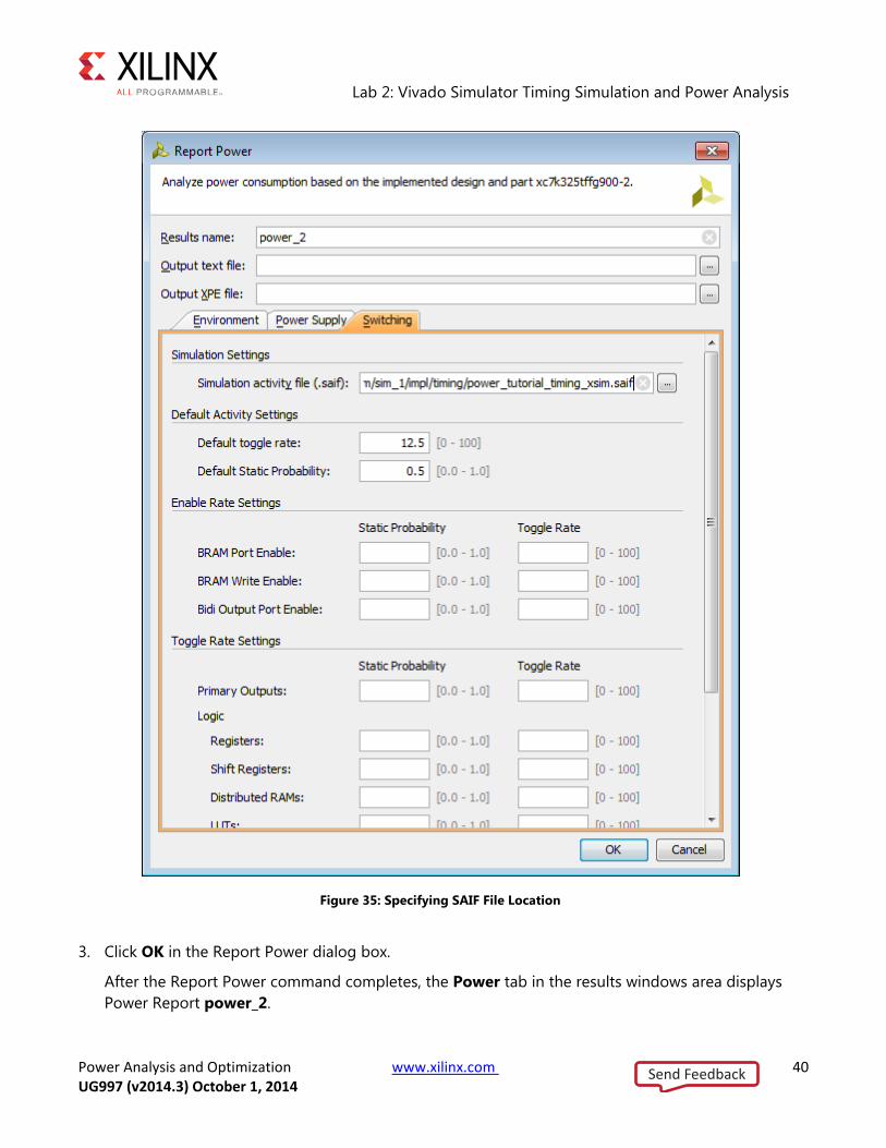
2. In the Report Power dialog box, specify the SAIF file location in the Switching tab.
The SAIF file, which was requested in the simulation settings prior to running timing simulation, should appear here:
/<project_directory>/power_tutorial1/power_tutorial1.sim/ sim_1/impl/timing/power_tutorial_timing_xsim.saif
Send Feedback
Lab 2: Vivado Simulator Timing Simulation and Power Analysis
Power Analysis and Optimization www.xilinx.com 40 UG997 (v2014.3) October 1, 2014
Figure 35: Specifying SAIF File Location
3. Click OK in the Report Power dialog box.
After the Report Power command completes, the Power tab in the results windows area displays Power Report power_2.
Send Feedback
Lab 2: Vivado Simulator Timing Simulation and Power Analysis
Power Analysis and Optimization www.xilinx.com 41 UG997 (v2014.3) October 1, 2014
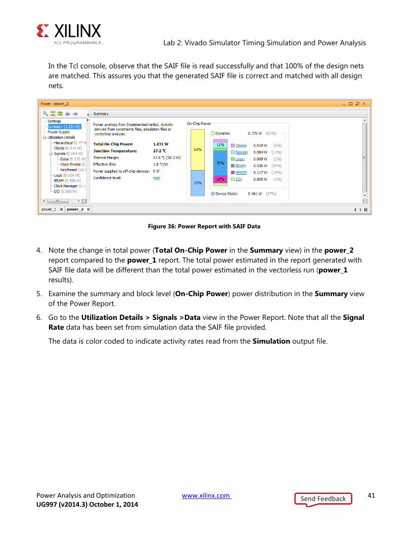
In the Tcl console, observe that the SAIF file is read successfully and that 100% of the design nets are matched. This assures you that the generated SAIF file is correct and matched with all design nets.
Figure 36: Power Report with SAIF Data
4. Note the change in total power (Total On-Chip Power in the Summary view) in the power_2 report compared to the power_1 report. The total power estimated in the report generated with SAIF file data will be different than the total power estimated in the vectorless run (power_1 results).
5. Examine the summary and block level (On-Chip Power) power distribution in the Summary view of the Power Report.
6. Go to the Utilization Details > Signals >Data view in the Power Report. Note that all the Signal Rate data has been set from simulation data the SAIF file provided.
The data is color coded to indicate activity rates read from the Simulation output file.
Send Feedback
Lab 2: Vivado Simulator Timing Simulation and Power Analysis
Power Analysis and Optimization www.xilinx.com 42 UG997 (v2014.3) October 1, 2014
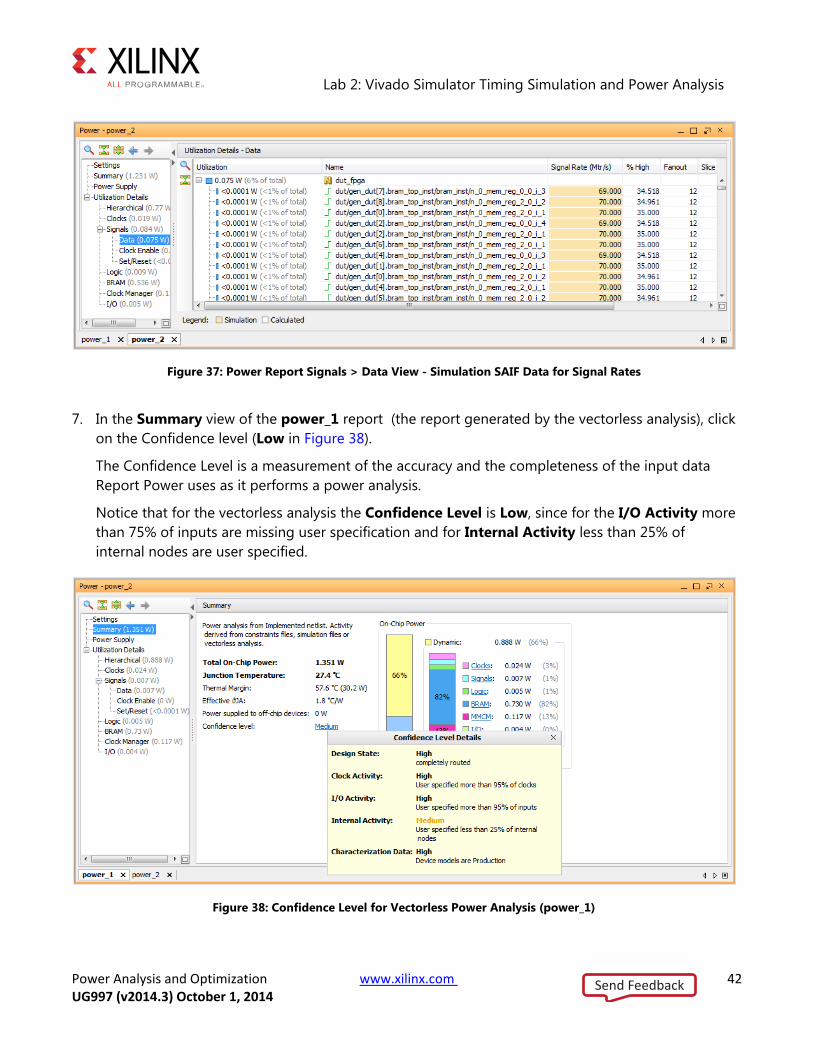
Figure 37: Power Report Signals > Data View - Simulation SAIF Data for Signal Rates
7. In the Summary view of the power_1 report (the report generated by the vectorless analysis), click on the Confidence level (Low in Figure 38).
The Confidence Level is a measurement of the accuracy and the completeness of the input data Report Power uses as it performs a power analysis.
Notice that for the vectorless analysis the Confidence Level is Low, since for the I/O Activity more than 75% of inputs are missing user specification and for Internal Activity less than 25% of internal nodes are user specified.
Figure 38: Confidence Level for Vectorless Power Analysis (power_1)
Send Feedback
Lab 2: Vivado Simulator Timing Simulation and Power Analysis
Power Analysis and Optimization www.xilinx.com 43 UG997 (v2014.3) October 1, 2014
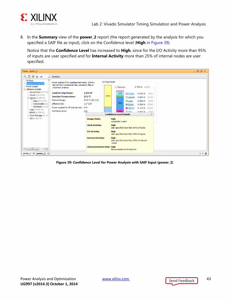
8. In the Summary view of the power_2 report (the report generated by the analysis for which you specified a SAIF file as input), click on the Confidence level (High in Figure 39).
Notice that the Confidence Level has increased to High, since for the I/O Activity more than 95% of inputs are user specified and for Internal Activity more than 25% of internal nodes are user specified.
Figure 39: Confidence Level for Power Analysis with SAIF Input (power_2)
Send Feedback
Power Analysis and Optimization www.xilinx.com 44 UG997 (v2014.3) October 1, 2014
Lab 3: QuestaSim Timing Simulation and Power Analysis
Introduction In this lab, you will learn about generating a SAIF file after running a timing level simulation using a QuestaSim simulator. The lab will take you through the steps for SAIF file creation, running timing simulation, and estimating power using the SAIF data.
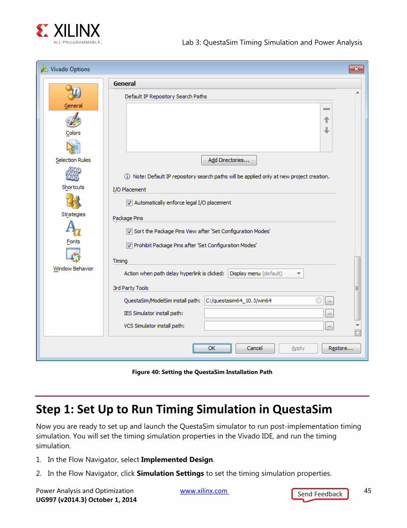
IMPORTANT: Make sure the Vivado Design Suite knows where to pick up the QuestaSim tool. You can either:
Manually set the path to ModelSim/QuestaSim using the $PATH environment variable
OR
From the Tools > Options > General dialog box, define the path to the simulator in the Vivado IDE under the 3rd Party Tools section: QuestaSim/ModelSim install path.
Send Feedback
Lab 3: QuestaSim Timing Simulation and Power Analysis
Power Analysis and Optimization www.xilinx.com 45 UG997 (v2014.3) October 1, 2014
Figure 40: Setting the QuestaSim Installation Path
Step 1: Set Up to Run Timing Simulation in QuestaSim Now you are ready to set up and launch the QuestaSim simulator to run post-implementation timing simulation. You will set the timing simulation properties in the Vivado IDE, and run the timing simulation.
1. In the Flow Navigator, select Implemented Design.
2. In the Flow Navigator, click Simulation Settings to set the timing simulation properties.
Send Feedback
Lab 3: QuestaSim Timing Simulation and Power Analysis
Power Analysis and Optimization www.xilinx.com 46 UG997 (v2014.3) October 1, 2014
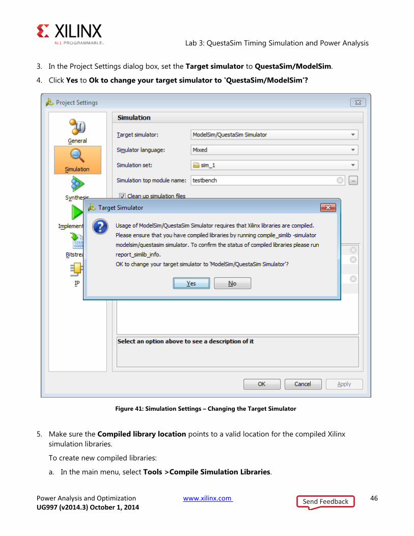
3. In the Project Settings dialog box, set the Target simulator to QuestaSim/ModelSim.
4. Click Yes to Ok to change your target simulator to ‛QuestaSim/ModelSim’?
Figure 41: Simulation Settings – Changing the Target Simulator
5. Make sure the Compiled library location points to a valid location for the compiled Xilinx simulation libraries.
To create new compiled libraries:
a. In the main menu, select Tools >Compile Simulation Libraries.
Send Feedback
Lab 3: QuestaSim Timing Simulation and Power Analysis
Power Analysis and Optimization www.xilinx.com 47 UG997 (v2014.3) October 1, 2014
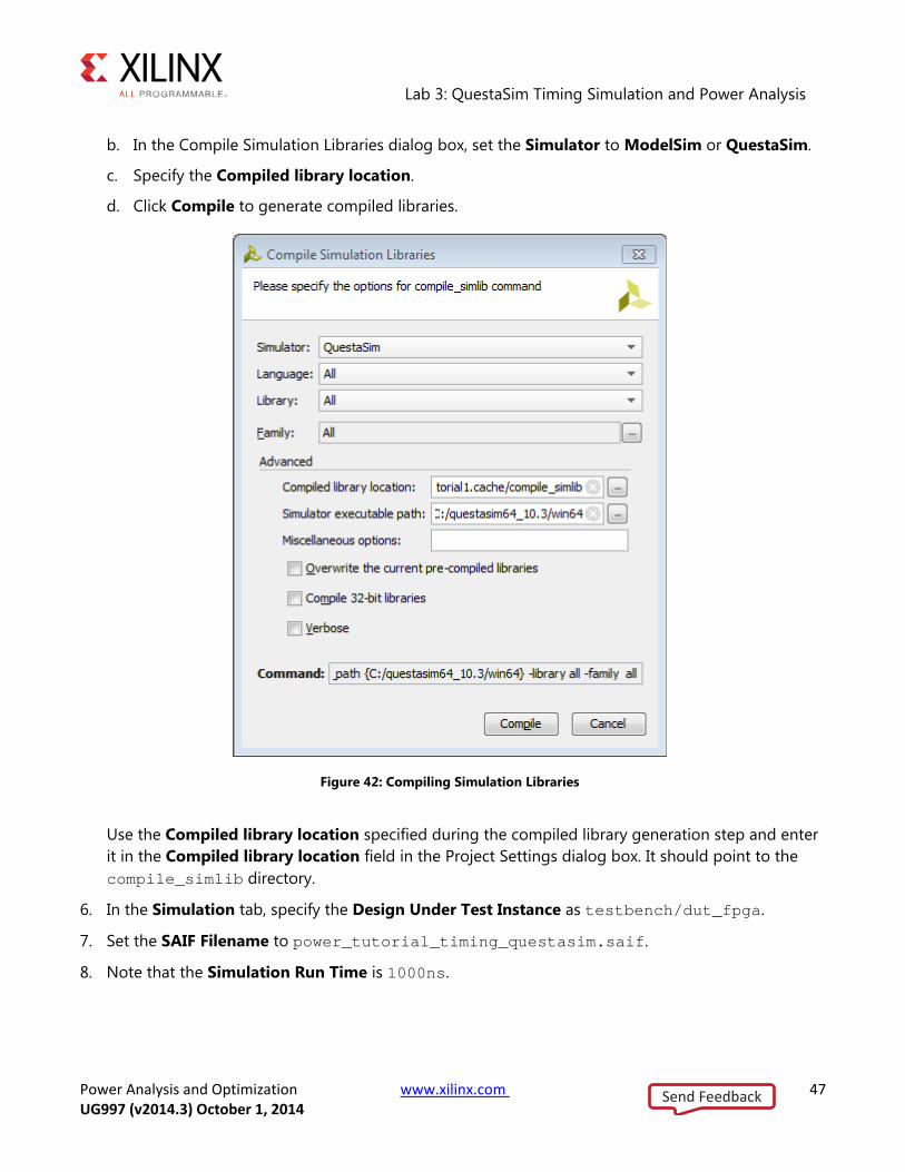
b. In the Compile Simulation Libraries dialog box, set the Simulator to ModelSim or QuestaSim.
c. Specify the Compiled library location.
d. Click Compile to generate compiled libraries.
Figure 42: Compiling Simulation Libraries
Use the Compiled library location specified during the compiled library generation step and enter it in the Compiled library location field in the Project Settings dialog box. It should point to the compile_simlib directory.
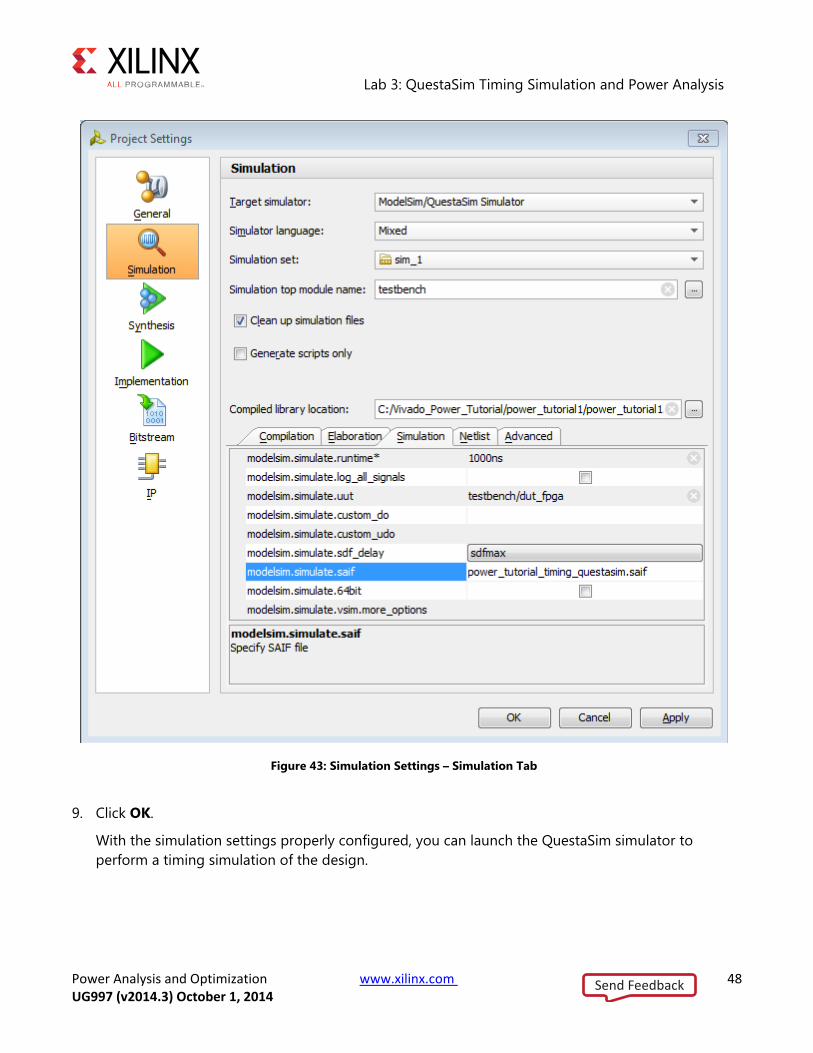
6. In the Simulation tab, specify the Design Under Test Instance as testbench/dut_fpga.
7. Set the SAIF Filename to power_tutorial_timing_questasim.saif.
8. Note that the Simulation Run Time is 1000ns.
Send Feedback
Lab 3: QuestaSim Timing Simulation and Power Analysis
Power Analysis and Optimization www.xilinx.com 48 UG997 (v2014.3) October 1, 2014
Figure 43: Simulation Settings – Simulation Tab
9. Click OK.
With the simulation settings properly configured, you can launch the QuestaSim simulator to perform a timing simulation of the design.
Send Feedback
Lab 3: QuestaSim Timing Simulation and Power Analysis
Power Analysis and Optimization www.xilinx.com 49 UG997 (v2014.3) October 1, 2014
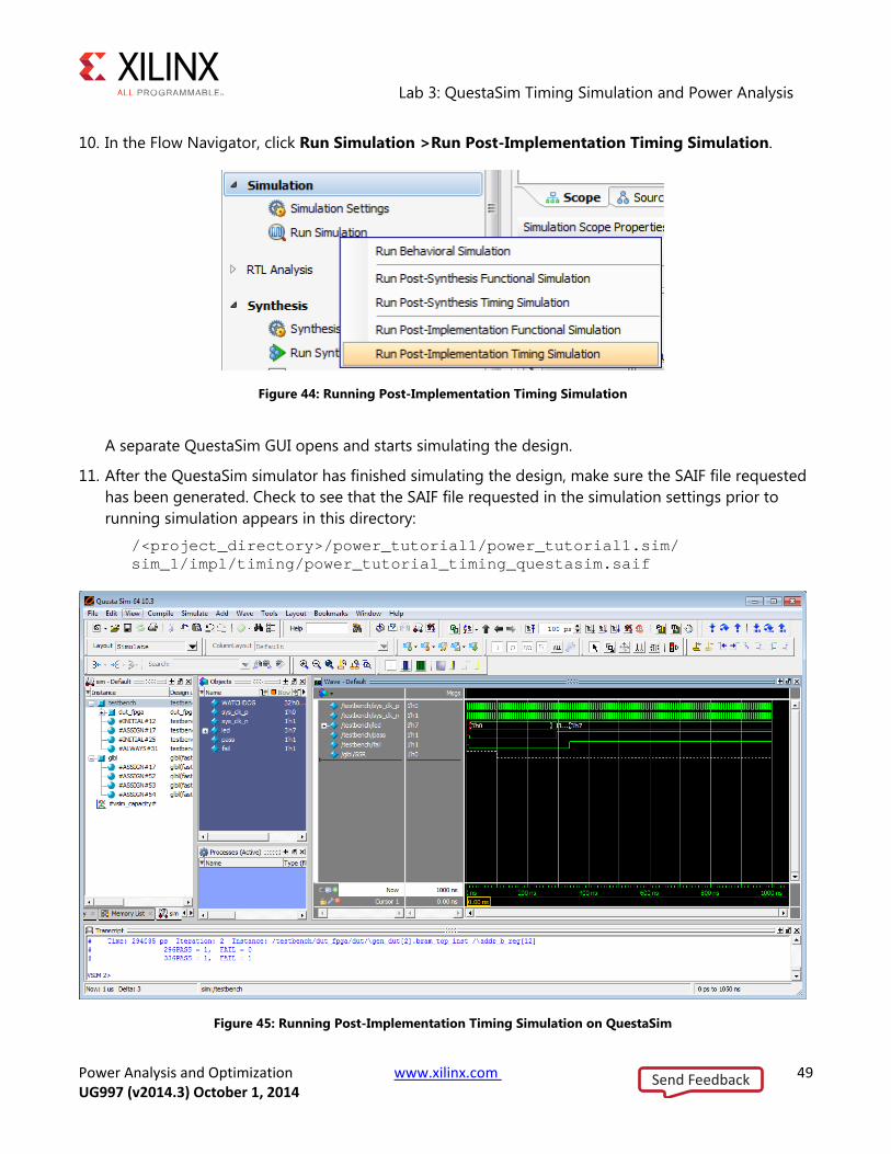
10. In the Flow Navigator, click Run Simulation >Run Post-Implementation Timing Simulation.
Figure 44: Running Post-Implementation Timing Simulation
A separate QuestaSim GUI opens and starts simulating the design.
11. After the QuestaSim simulator has finished simulating the design, make sure the SAIF file requested has been generated. Check to see that the SAIF file requested in the simulation settings prior to running simulation appears in this directory:
/<project_directory>/power_tutorial1/power_tutorial1.sim/ sim_1/impl/timing/power_tutorial_timing_questasim.saif
Figure 45: Running Post-Implementation Timing Simulation on QuestaSim
Send Feedback
Lab 3: QuestaSim Timing Simulation and Power Analysis
Power Analysis and Optimization www.xilinx.com 50 UG997 (v2014.3) October 1, 2014
Step 2: Running Report Power in Vectorless Mode
IMPORTANT: If SAIF based report_power has already been run in this session, run the reset_switching_activity -all command in the Tcl Console. This will clear the SAIF data in the power engine from the earlier runs.
1. Close any open Report Power views.
2. In the Flow Navigator, select Implemented Design > Report Power to open the Report Power dialog box.
Alternatively, select Tools > Report > Report Power in the main menu bar.
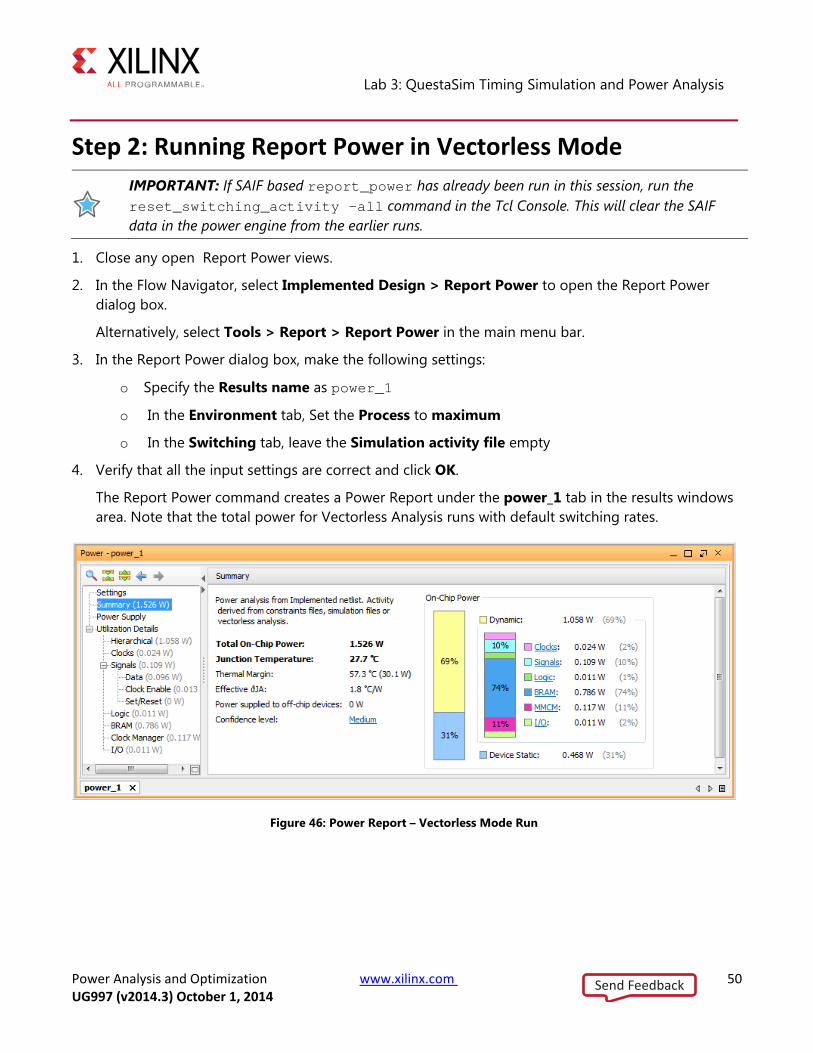
3. In the Report Power dialog box, make the following settings:
o Specify the Results name as power_1
o In the Environment tab, Set the Process to maximum
o In the Switching tab, leave the Simulation activity file empty
4. Verify that all the input settings are correct and click OK.
The Report Power command creates a Power Report under the power_1 tab in the results windows area. Note that the total power for Vectorless Analysis runs with default switching rates.
Figure 46: Power Report – Vectorless Mode Run
Send Feedback
Lab 3: QuestaSim Timing Simulation and Power Analysis
Power Analysis and Optimization www.xilinx.com 51 UG997 (v2014.3) October 1, 2014
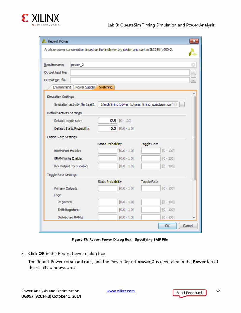
Step 3: Running Report Power with QuestaSim SAIF Data The SAIF output file requested in the simulation run has been generated under the project directory. We use this SAIF file – a “Switching Activity Interchange Format” file – to further guide the power estimation algorithm.
1. In the main menu bar, select Tools > Report > Report Power.
2. In the Report Power dialog box, specify the SAIF file location in the Switching tab.
The SAIF file, which was requested in the simulation settings prior to running simulation, should appear here:
/<project_directory>/power_tutorial1/ power_tutorial1.sim/ sim_1/impl/timing/power_tutorial_timing_questasim.saif
Send Feedback
Lab 3: QuestaSim Timing Simulation and Power Analysis
Power Analysis and Optimization www.xilinx.com 52 UG997 (v2014.3) October 1, 2014
Figure 47: Report Power Dialog Box – Specifying SAIF File
3. Click OK in the Report Power dialog box.
The Report Power command runs, and the Power Report power_2 is generated in the Power tab of the results windows area.
Send Feedback
Lab 3: QuestaSim Timing Simulation and Power Analysis
Power Analysis and Optimization www.xilinx.com 53 UG997 (v2014.3) October 1, 2014
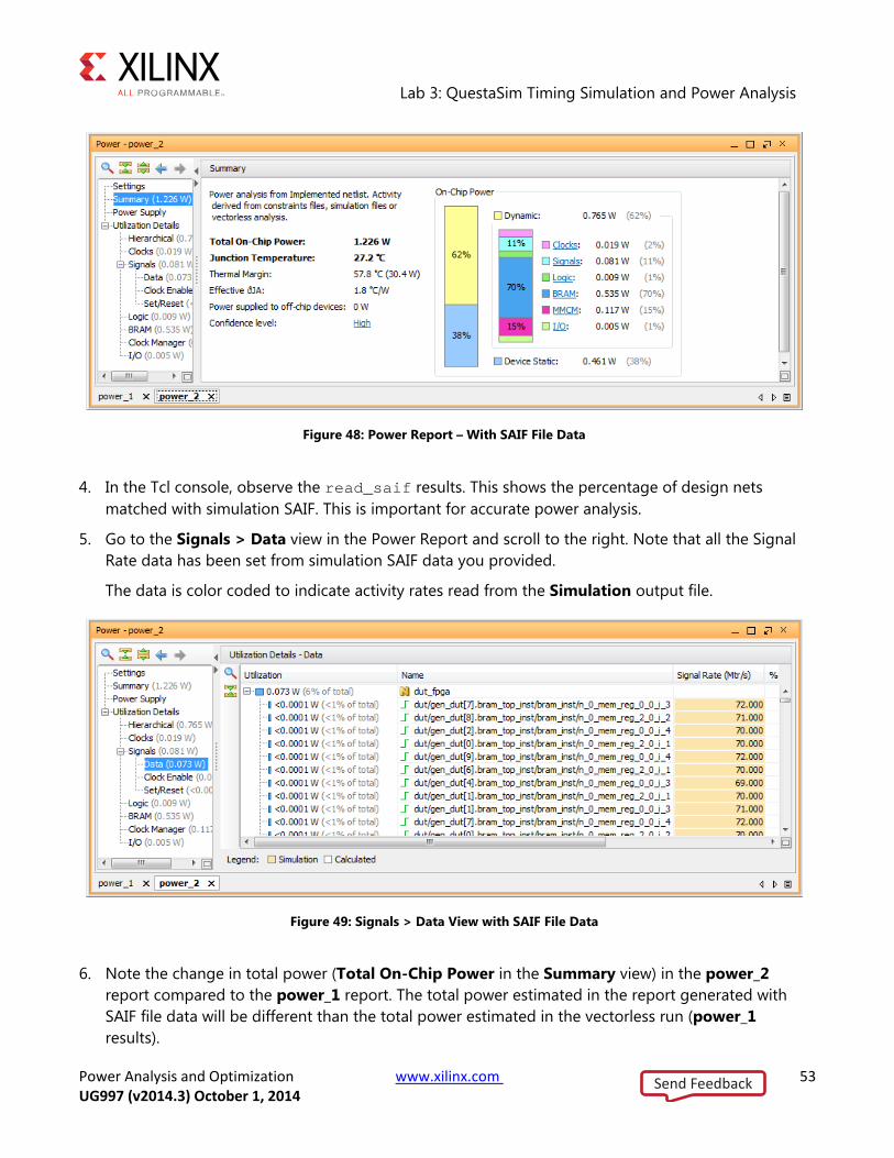
Figure 48: Power Report – With SAIF File Data
4. In the Tcl console, observe the read_saif results. This shows the percentage of design nets matched with simulation SAIF. This is important for accurate power analysis.
5. Go to the Signals > Data view in the Power Report and scroll to the right. Note that all the Signal Rate data has been set from simulation SAIF data you provided.
The data is color coded to indicate activity rates read from the Simulation output file.
Figure 49: Signals > Data View with SAIF File Data
6. Note the change in total power (Total On-Chip Power in the Summary view) in the power_2 report compared to the power_1 report. The total power estimated in the report generated with SAIF file data will be different than the total power estimated in the vectorless run (power_1 results).
Send Feedback
Lab 4: Hardware Power Measurement Using the KC705 Evaluation Board
Power Analysis and Optimization www.xilinx.com 54 UG997 (v2014.3) October 1, 2014
Lab 4: Hardware Power Measurement Using the KC705 Evaluation Board
Introduction In this lab, you will learn about basic hardware power measurement technique and correlating the hardware power numbers with the numbers generated by Vivado Report Power. The lab will take you through the steps for setting up the hardware measurement, programing a bit file using Vivado Hardware Manager and power measurement through Texas Instruments (TI) Fusion Design Software. It also includes Junction Temperature reading from Vivado System Monitor.
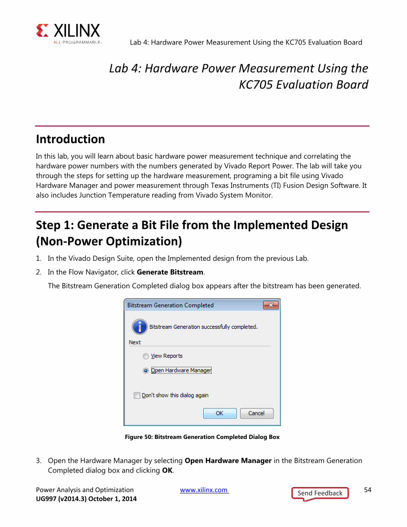
Step 1: Generate a Bit File from the Implemented Design (Non-Power Optimization) 1. In the Vivado Design Suite, open the Implemented design from the previous Lab.
2. In the Flow Navigator, click Generate Bitstream.
The Bitstream Generation Completed dialog box appears after the bitstream has been generated.
Figure 50: Bitstream Generation Completed Dialog Box
3. Open the Hardware Manager by selecting Open Hardware Manager in the Bitstream Generation Completed dialog box and clicking OK.
Send Feedback
Lab 4: Hardware Power Measurement Using the KC705 Evaluation Board
Power Analysis and Optimization www.xilinx.com 55 UG997 (v2014.3) October 1, 2014
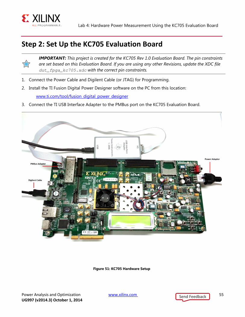
Step 2: Set Up the KC705 Evaluation Board
IMPORTANT: This project is created for the KC705 Rev 1.0 Evaluation Board. The pin constraints are set based on this Evaluation Board. If you are using any other Revisions, update the XDC file dut_fpga_kc705.xdc with the correct pin constraints.
1. Connect the Power Cable and Digilent Cable (or JTAG) for Programming.
2. Install the TI Fusion Digital Power Designer software on the PC from this location:
www.ti.com/tool/fusion_digital_power_designer
3. Connect the TI USB Interface Adapter to the PMBus port on the KC705 Evaluation Board.
Figure 51: KC705 Hardware Setup
Send Feedback
Lab 4: Hardware Power Measurement Using the KC705 Evaluation Board
Power Analysis and Optimization www.xilinx.com 56 UG997 (v2014.3) October 1, 2014
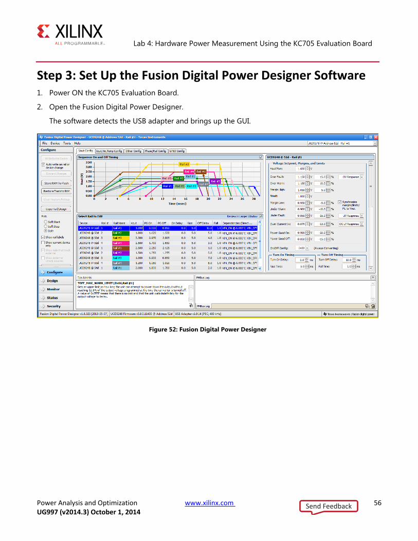
Step 3: Set Up the Fusion Digital Power Designer Software 1. Power ON the KC705 Evaluation Board.
2. Open the Fusion Digital Power Designer.
The software detects the USB adapter and brings up the GUI.
Figure 52: Fusion Digital Power Designer
Send Feedback
Lab 4: Hardware Power Measurement Using the KC705 Evaluation Board
Power Analysis and Optimization www.xilinx.com 57 UG997 (v2014.3) October 1, 2014
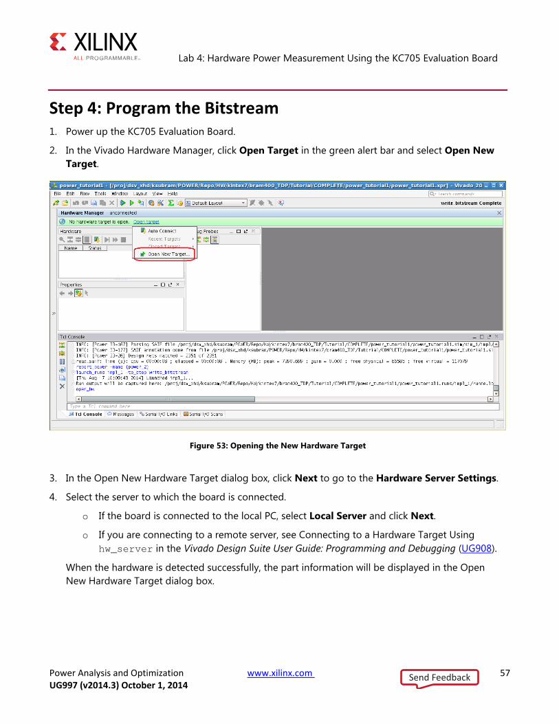
Step 4: Program the Bitstream 1. Power up the KC705 Evaluation Board.
2. In the Vivado Hardware Manager, click Open Target in the green alert bar and select Open New Target.
Figure 53: Opening the New Hardware Target
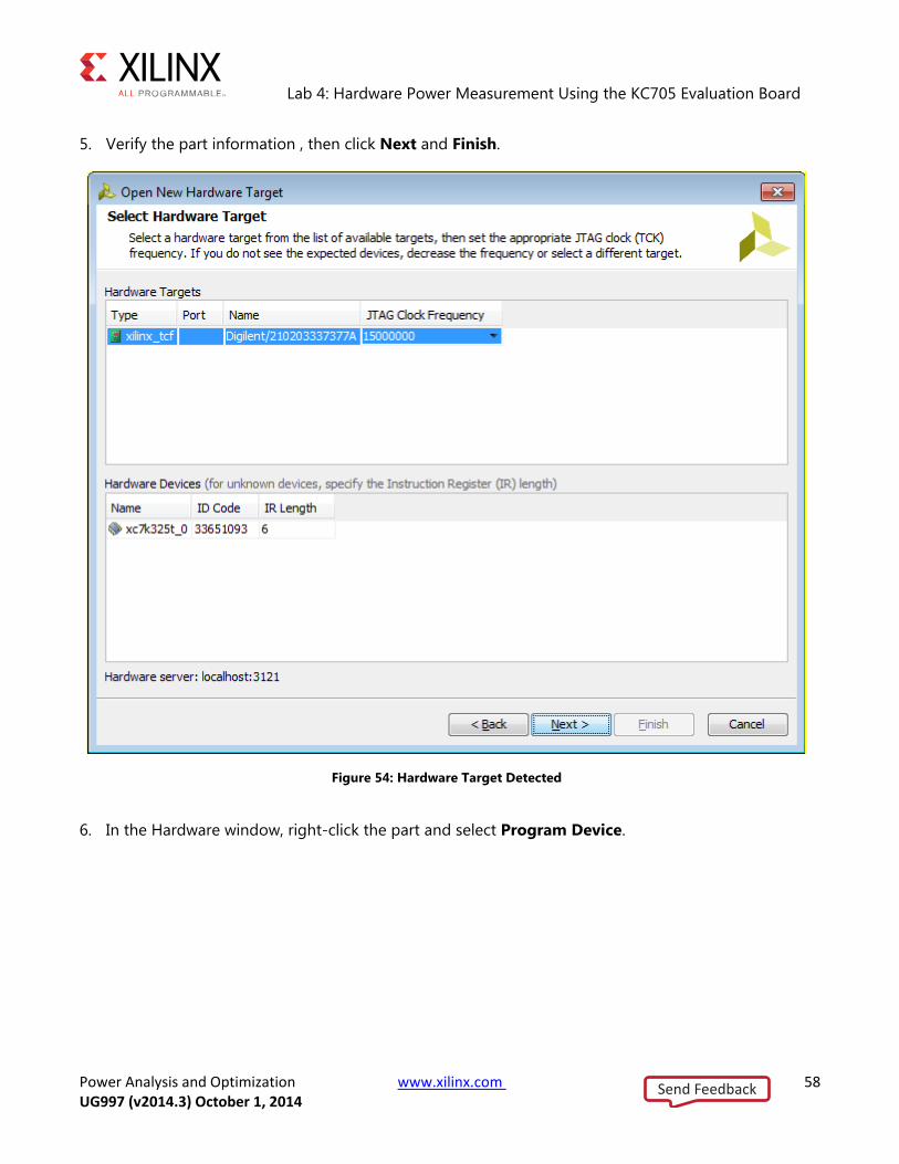
3. In the Open New Hardware Target dialog box, click Next to go to the Hardware Server Settings.
4. Select the server to which the board is connected.
o If the board is connected to the local PC, select Local Server and click Next.
o If you are connecting to a remote server, see Connecting to a Hardware Target Using hw_server in the Vivado Design Suite User Guide: Programming and Debugging (UG908).
When the hardware is detected successfully, the part information will be displayed in the Open New Hardware Target dialog box.
Send Feedback
Lab 4: Hardware Power Measurement Using the KC705 Evaluation Board
Power Analysis and Optimization www.xilinx.com 58 UG997 (v2014.3) October 1, 2014
5. Verify the part information , then click Next and Finish.
Figure 54: Hardware Target Detected
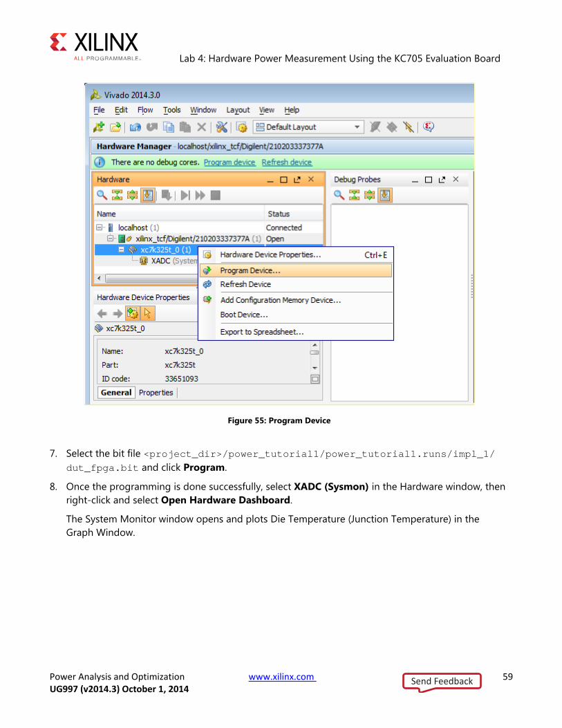
6. In the Hardware window, right-click the part and select Program Device.
Send Feedback
Lab 4: Hardware Power Measurement Using the KC705 Evaluation Board
Power Analysis and Optimization www.xilinx.com 59 UG997 (v2014.3) October 1, 2014
Figure 55: Program Device
7. Select the bit file <project_dir>/power_tutorial1/power_tutorial1.runs/impl_1/ dut_fpga.bit and click Program.
8. Once the programming is done successfully, select XADC (Sysmon) in the Hardware window, then right-click and select Open Hardware Dashboard.
The System Monitor window opens and plots Die Temperature (Junction Temperature) in the Graph Window.
Send Feedback
Lab 4: Hardware Power Measurement Using the KC705 Evaluation Board
Power Analysis and Optimization www.xilinx.com 60 UG997 (v2014.3) October 1, 2014
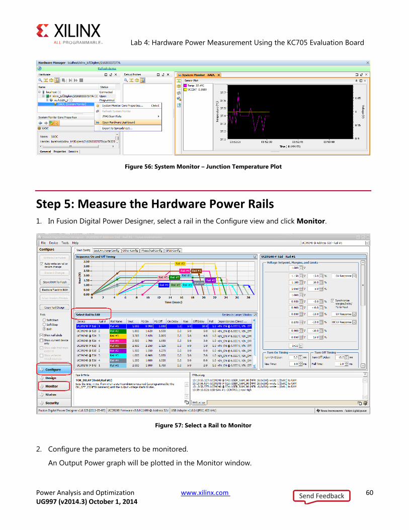
Figure 56: System Monitor – Junction Temperature Plot
Step 5: Measure the Hardware Power Rails 1. In Fusion Digital Power Designer, select a rail in the Configure view and click Monitor.
Figure 57: Select a Rail to Monitor
2. Configure the parameters to be monitored.
An Output Power graph will be plotted in the Monitor window.
Send Feedback
Lab 4: Hardware Power Measurement Using the KC705 Evaluation Board
Power Analysis and Optimization www.xilinx.com 61 UG997 (v2014.3) October 1, 2014
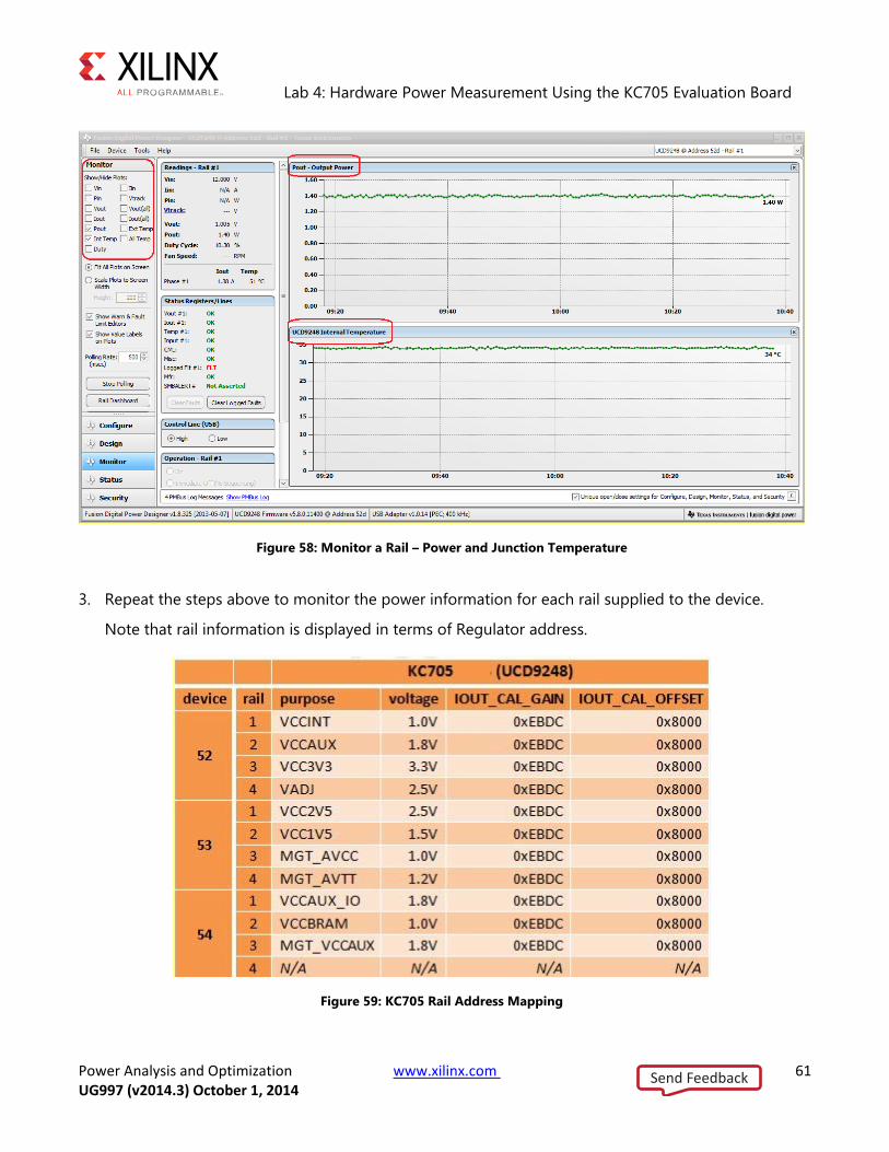
Figure 58: Monitor a Rail – Power and Junction Temperature
3. Repeat the steps above to monitor the power information for each rail supplied to the device.
Note that rail information is displayed in terms of Regulator address.
Figure 59: KC705 Rail Address Mapping
Send Feedback
Lab 4: Hardware Power Measurement Using the KC705 Evaluation Board
Power Analysis and Optimization www.xilinx.com 62 UG997 (v2014.3) October 1, 2014
4. Note down the Junction Temperature value either from the Vivado Hardware Manager or from Fusion Digital Power Designer.
Vectorless Power Estimation with Junction Temperature For further Power Analysis, you can use the measured Junction Temperature and other thermal settings to feed into Vivado Report Power for better accuracy.
1. In the Vivado Design Suite, open the tutorial project and click Open Implemented Design to display the implemented design.
2. In the Tcl Console, run the following command to reset any user defined or SAIF file defined settings.
reset_switching_activity -all
3. In the main menu bar, select Tools > Report > Report Power.
4. In the Report Power dialog box Environment tab, enter the Junction Temperature value supplied by the hardware power measurement.
5. Set the Process to maximum.
6. In the Switching tab, make sure the Simulation activity file (saif) is blank.
7. Click OK.
Send Feedback
Lab 4: Hardware Power Measurement Using the KC705 Evaluation Board
Power Analysis and Optimization www.xilinx.com 63 UG997 (v2014.3) October 1, 2014
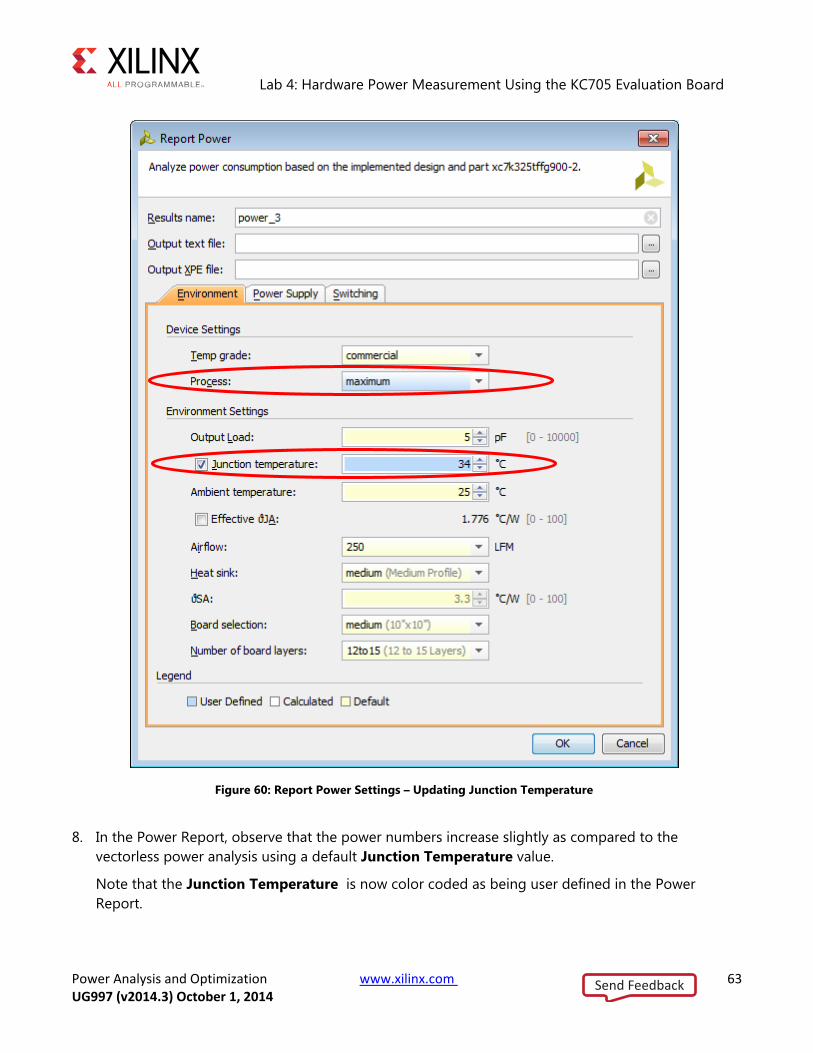
Figure 60: Report Power Settings – Updating Junction Temperature
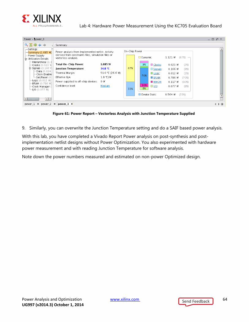
8. In the Power Report, observe that the power numbers increase slightly as compared to the vectorless power analysis using a default Junction Temperature value.
Note that the Junction Temperature is now color coded as being user defined in the Power Report.
Send Feedback
Lab 4: Hardware Power Measurement Using the KC705 Evaluation Board
Power Analysis and Optimization www.xilinx.com 64 UG997 (v2014.3) October 1, 2014
Figure 61: Power Report – Vectorless Analysis with Junction Temperature Supplied
9. Similarly, you can overwrite the Junction Temperature setting and do a SAIF based power analysis.
With this lab, you have completed a Vivado Report Power analysis on post-synthesis and post-implementation netlist designs without Power Optimization. You also experimented with hardware power measurement and with reading Junction Temperature for software analysis.
Note down the power numbers measured and estimated on non-power Optimized design.
Send Feedback

Power Analysis and Optimization www.xilinx.com 65 UG997 (v2014.3) October 1, 2014
Lab 5: Power Optimization in Vivado
Introduction In this lab, you will learn about using the Power Optimization features in Vivado. The lab will take you through the steps for invoking Power Optimization after synthesizing the design. It will also guide on using the power optimization report, making decisions and selectively turning off power optimization on signals, blocks, and hierarchies.
TIP: When you run Implementation on your design, the Vivado tools may perform BRAM power optimizations by default during opt_design. These optimizations will not affect performance, and will have little impact on area and runtime. In the previous Lab, the default BRAM power optimization was disabled by setting a NoBramPowerOpt directive to opt_design.
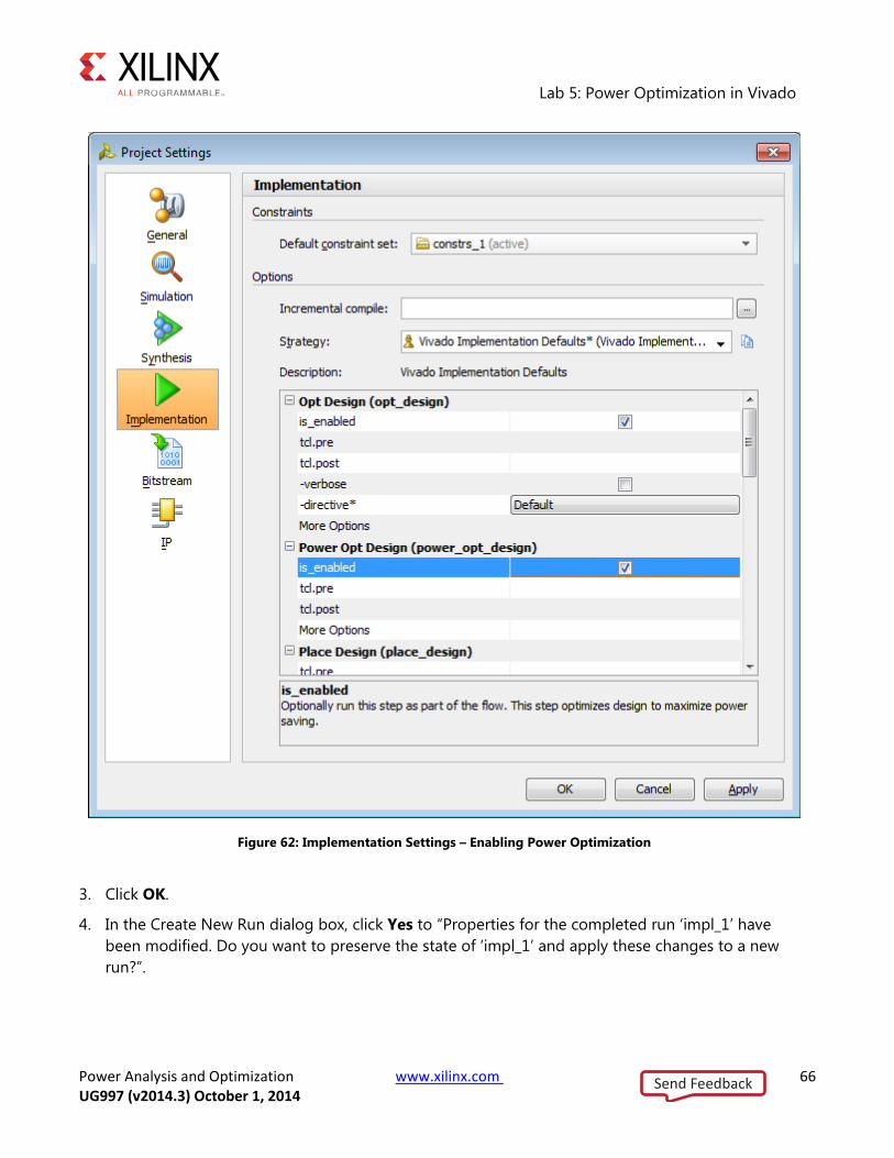
Step 1: Set Up Options to Run Power Optimization 1. In the Flow Navigator, click Implementation Settings.
2. In the Project Settings dialog box, make these settings:
o In the Opt Design settings, set the –directive option to Default.
BRAM optimization runs in the Default setting for Opt Design during Implementation. BRAM optimization was disabled in the previous lab. It is now re-enabled when the design runs Power Optimization.
o In the Power Opt Design settings, check the is_enabled box.
This ensures Power Optimization runs after opt_design. Enabling the Power Opt Design option prior to place_design results in a complete power optimization to be performed. This option yields the best possible power saving from Vivado.
Send Feedback
Lab 5: Power Optimization in Vivado
Power Analysis and Optimization www.xilinx.com 66 UG997 (v2014.3) October 1, 2014
Figure 62: Implementation Settings – Enabling Power Optimization
3. Click OK.
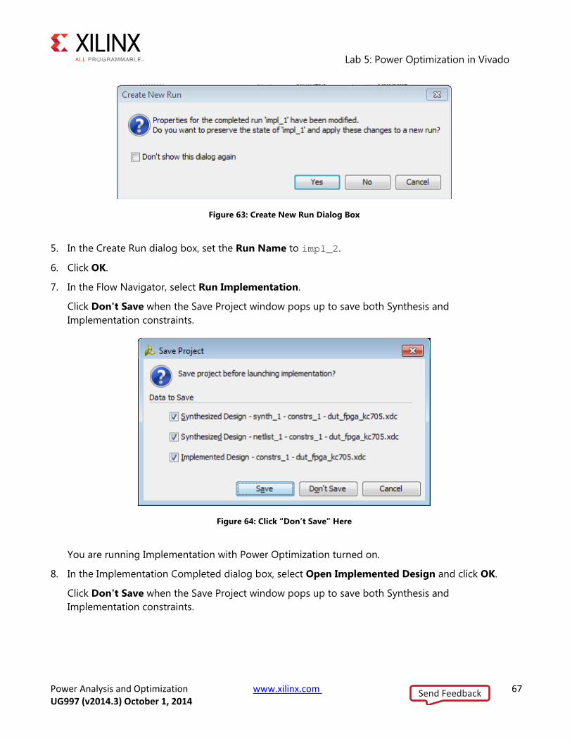
4. In the Create New Run dialog box, click Yes to “Properties for the completed run ‘impl_1’ have been modified. Do you want to preserve the state of ‘impl_1’ and apply these changes to a new run?”.
Send Feedback
Lab 5: Power Optimization in Vivado
Power Analysis and Optimization www.xilinx.com 67 UG997 (v2014.3) October 1, 2014
Figure 63: Create New Run Dialog Box
5. In the Create Run dialog box, set the Run Name to impl_2.
6. Click OK.
7. In the Flow Navigator, select Run Implementation.
Click Don't Save when the Save Project window pops up to save both Synthesis and Implementation constraints.
Figure 64: Click “Don’t Save” Here
You are running Implementation with Power Optimization turned on.
8. In the Implementation Completed dialog box, select Open Implemented Design and click OK.
Click Don't Save when the Save Project window pops up to save both Synthesis and Implementation constraints.
Send Feedback
Lab 5: Power Optimization in Vivado
Power Analysis and Optimization www.xilinx.com 68 UG997 (v2014.3) October 1, 2014
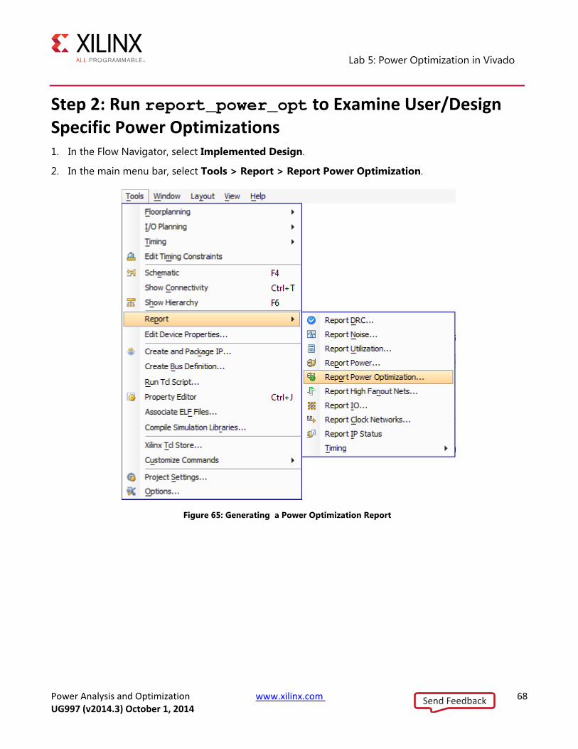
Step 2: Run report_power_opt to Examine User/Design Specific Power Optimizations 1. In the Flow Navigator, select Implemented Design.
2. In the main menu bar, select Tools > Report > Report Power Optimization.
Figure 65: Generating a Power Optimization Report
Send Feedback
Lab 5: Power Optimization in Vivado
Power Analysis and Optimization www.xilinx.com 69 UG997 (v2014.3) October 1, 2014
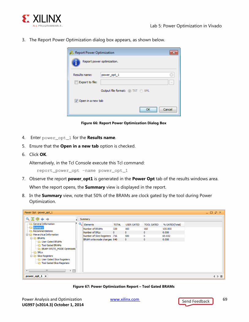
3. The Report Power Optimization dialog box appears, as shown below.
Figure 66: Report Power Optimization Dialog Box
4. Enter power_opt_1 for the Results name.
5. Ensure that the Open in a new tab option is checked.
6. Click OK.
Alternatively, in the Tcl Console execute this Tcl command:
report_power_opt -name power_opt_1
7. Observe the report power_opt1 is generated in the Power Opt tab of the results windows area.
When the report opens, the Summary view is displayed in the report.
8. In the Summary view, note that 50% of the BRAMs are clock gated by the tool during Power Optimization.
Figure 67: Power Optimization Report – Tool Gated BRAMs
Send Feedback
Lab 5: Power Optimization in Vivado
Power Analysis and Optimization www.xilinx.com 70 UG997 (v2014.3) October 1, 2014
9. In the Power Report, select Hierarchical Information > BRAMs > Tool Gated BRAMs and observe the detailed information on tool gated BRAM enables.
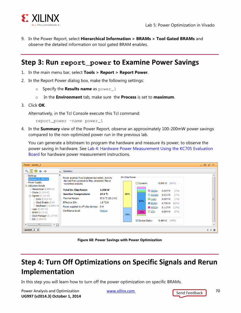
Step 3: Run report_power to Examine Power Savings 1. In the main menu bar, select Tools > Report > Report Power.
2. In the Report Power dialog box, make the following settings:
o Specify the Results name as power_1
o In the Environment tab, make sure the Process is set to maximum.
3. Click OK.
Alternatively, in the Tcl Console execute this Tcl command:
report_power -name power_1
4. In the Summary view of the Power Report, observe an approximately 100-200mW power savings compared to the non-optimized power run in the previous lab.
You can generate a bitstream to program the hardware and measure its power, to observe the power saving in hardware. See Lab 4: Hardware Power Measurement Using the KC705 Evaluation Board for hardware power measurement instructions.
Figure 68: Power Savings with Power Optimization
Step 4: Turn Off Optimizations on Specific Signals and Rerun Implementation In this step you will learn how to turn off the power optimization on specific BRAMs.
Send Feedback
Lab 5: Power Optimization in Vivado
Power Analysis and Optimization www.xilinx.com 71 UG997 (v2014.3) October 1, 2014
IMPORTANT: Power optimization works to minimize the impact on timing while maximizing power savings. However, in certain cases, if timing degrades after power optimization, you can identify and apply power optimizations only on non-timing critical clock domains or modules using the set_power_opt XDC command. Refer to the Vivado Design Suite User Guide: Power Analysis and Optimization (UG907) for more information on the set_power_opt command.
Let us assume that this BRAM is in the critical path:
dut/gen_dut[0].bram_top_inst/bram_inst/mem_reg_0_0
This step makes sure the tool does not gate this BRAM.
1. In the Tcl Console, type this command:
set_power_opt -exclude_cells [get_cells dut/gen_dut[0].bram_top_inst/bram_inst/mem_reg_0_0]
This will prevent the tool from gating this BRAM.
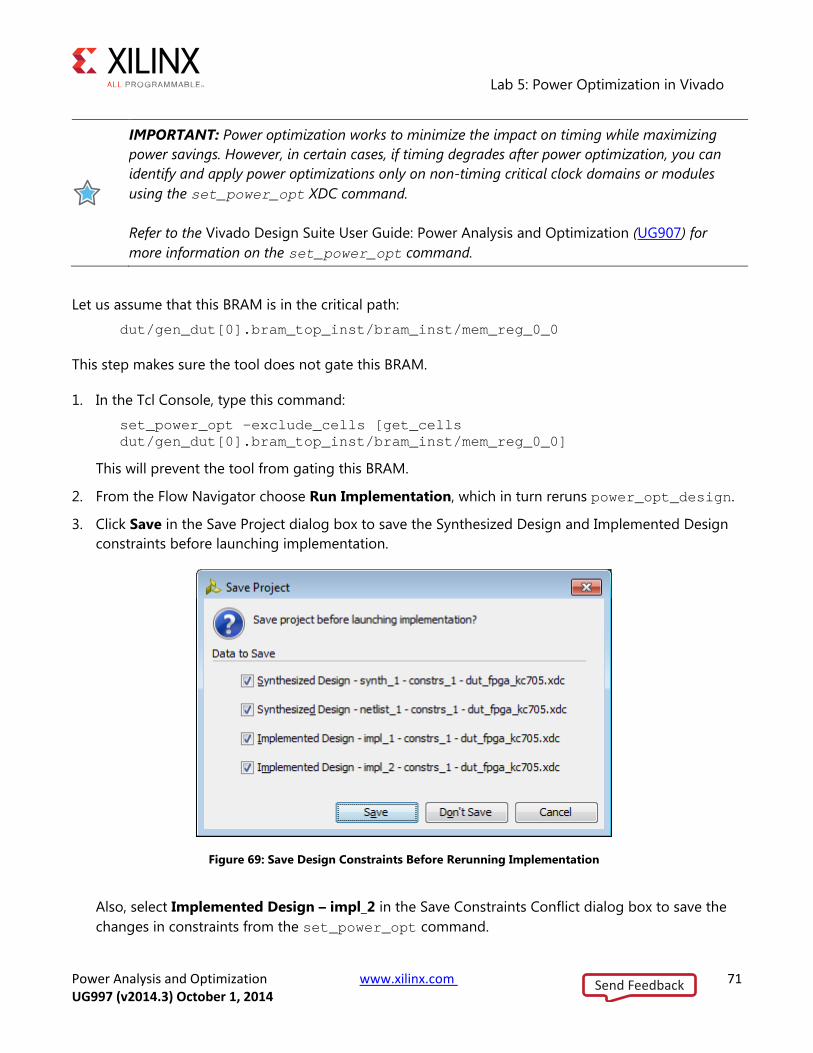
2. From the Flow Navigator choose Run Implementation, which in turn reruns power_opt_design.
3. Click Save in the Save Project dialog box to save the Synthesized Design and Implemented Design constraints before launching implementation.
Figure 69: Save Design Constraints Before Rerunning Implementation
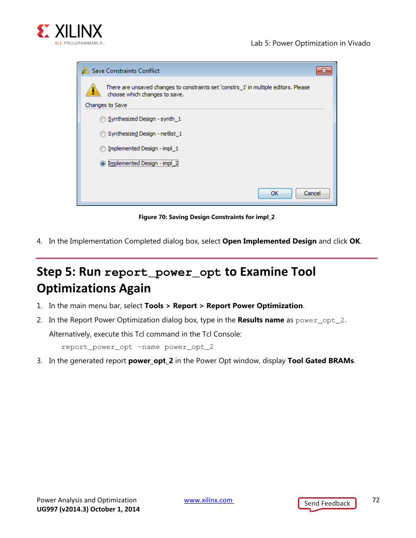
Also, select Implemented Design – impl_2 in the Save Constraints Conflict dialog box to save the changes in constraints from the set_power_opt command.
Send Feedback
Lab 5: Power Optimization in Vivado
Power Analysis and Optimization www.xilinx.com 72 UG997 (v2014.3) October 1, 2014
Figure 70: Saving Design Constraints for impl_2
4. In the Implementation Completed dialog box, select Open Implemented Design and click OK.
Step 5: Run report_power_opt to Examine Tool Optimizations Again 1. In the main menu bar, select Tools > Report > Report Power Optimization.
2. In the Report Power Optimization dialog box, type in the Results name as power_opt_2.
Alternatively, execute this Tcl command in the Tcl Console:
report_power_opt -name power_opt_2
3. In the generated report power_opt_2 in the Power Opt window, display Tool Gated BRAMs.
Send Feedback
Lab 5: Power Optimization in Vivado
Power Analysis and Optimization www.xilinx.com 73 UG997 (v2014.3) October 1, 2014
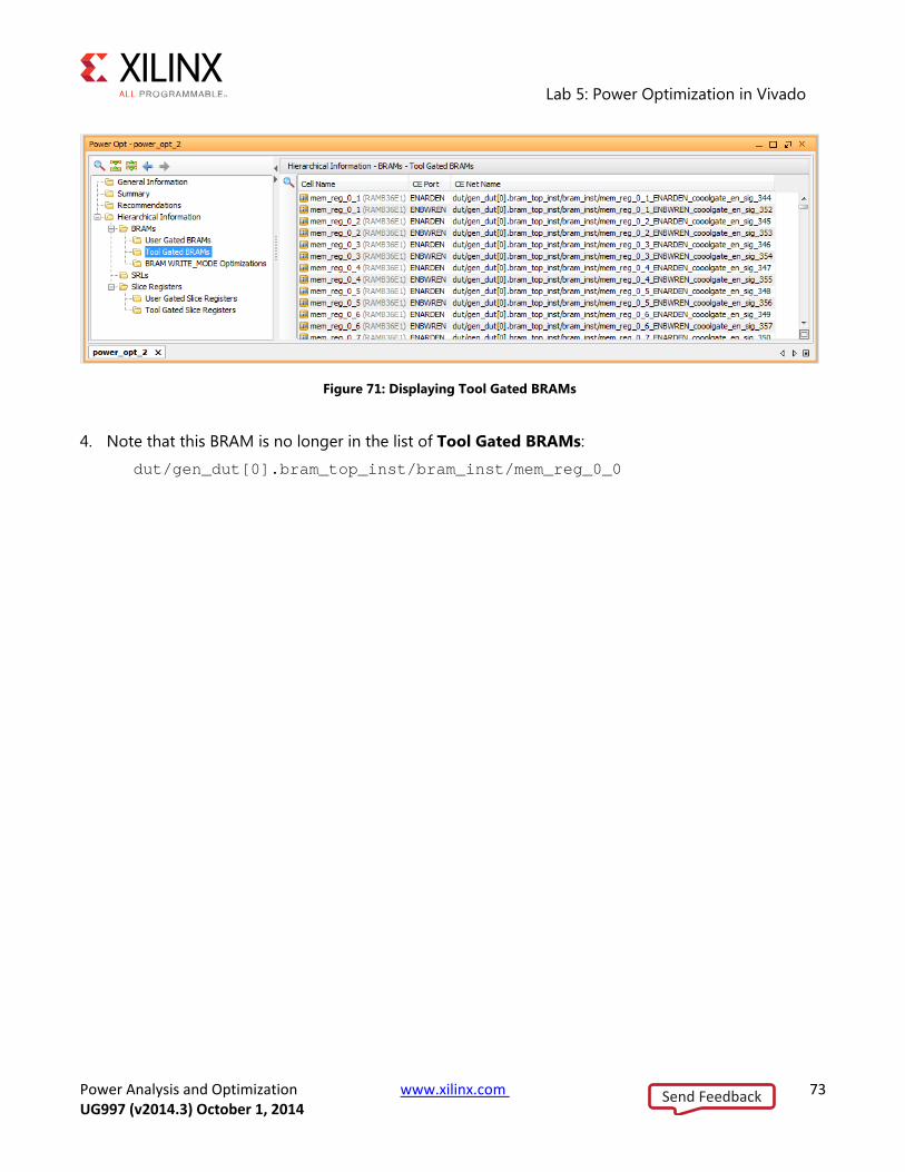
Figure 71: Displaying Tool Gated BRAMs
4. Note that this BRAM is no longer in the list of Tool Gated BRAMs:
dut/gen_dut[0].bram_top_inst/bram_inst/mem_reg_0_0
Send Feedback
Lab 5: Power Optimization in Vivado
Power Analysis and Optimization www.xilinx.com 74 UG997 (v2014.3) October 1, 2014
Conclusion In this tutorial, you accomplished the following:
• Used the Report Power dialog box to verify and set device, thermal, and environmental conditions that contribute to power estimation.
• Synthesized the design and estimated the power after synthesis.
• Set switching activities on an I/O port and reran Report Power.
• Ran functional simulation using the Vivado Simulator and generated a SAIF file that is input to Report Power for a more accurate power analysis.
• Implemented the design, ran post-implementation timing simulation using the Vivado Simulator, and generated a SAIF file that is input to report power for a more accurate power analysis.
• Ran QuestaSim post-implementation timing simulation and generated a SAIF file that is input to report power for a more accurate power analysis.
• Performed power measurement on the design implemented in a KC705 Evaluation Board. Compared the hardware power numbers with the numbers generated by Vivado Report Power.
• Learned how to invoke power optimization as part of an implementation run.
• Examined the power optimization report and selectively turned off power optimizations on a cell in the design.
Send Feedback

Power Analysis and Optimization www.xilinx.com 75 UG997 (v2014.3) October 1, 2014
Legal Notices
Please Read: Important Legal Notices The information disclosed to you hereunder (the “Materials”) is provided solely for the selection and use of Xilinx products. To the maximum extent permitted by applicable law: (1) Materials are made available "AS IS" and with all faults, Xilinx hereby DISCLAIMS ALL WARRANTIES AND CONDITIONS, EXPRESS, IMPLIED, OR STATUTORY, INCLUDING BUT NOT LIMITED TO WARRANTIES OF MERCHANTABILITY, NON-INFRINGEMENT, OR FITNESS FOR ANY PARTICULAR PURPOSE; and (2) Xilinx shall not be liable (whether in contract or tort, including negligence, or under any other theory of liability) for any loss or damage of any kind or nature related to, arising under, or in connection with, the Materials (including your use of the Materials), including for any direct, indirect, special, incidental, or consequential loss or damage (including loss of data, profits, goodwill, or any type of loss or damage suffered as a result of any action brought by a third party) even if such damage or loss was reasonably foreseeable or Xilinx had been advised of the possibility of the same. Xilinx assumes no obligation to correct any errors contained in the Materials or to notify you of updates to the Materials or to product specifications. You may not reproduce, modify, distribute, or publicly display the Materials without prior written consent. Certain products are subject to the terms and conditions of Xilinx’s limited warranty, please refer to Xilinx’s Terms of Sale which can be viewed at http://www.xilinx.com/legal.htm#tos; IP cores may be subject to warranty and support terms contained in a license issued to you by Xilinx. Xilinx products are not designed or intended to be fail-safe or for use in any application requiring fail-safe performance; you assume sole risk and liability for use of Xilinx products in such critical applications, please refer to Xilinx’s Terms of Sale which can be viewed at http://www.xilinx.com/legal.htm#tos.
© Copyright 2013-2014 Xilinx, Inc. Xilinx, the Xilinx logo, Artix, ISE, Kintex, Spartan, Virtex, Zynq, and other designated brands included herein are trademarks of Xilinx in the United States and other countries. All other trademarks are the property of their respective owner.
Send Feedback