Embed Size (px)
Citation preview
R
Virtex-5 CPRI Protocol Standard
Characterization Test Report
RPT066 (v1.0.1) June 22, 2007

Virtex-5 CPRI Protocol Standard www.xilinx.com RPT066 (v1.0.1) June 22, 2007
Xilinx is disclosing this Document and Intellectual Property (hereinafter “the Design”) to you for use in the development of designs to operate on, or interface with Xilinx FPGAs. Except as stated herein, none of the Design may be copied, reproduced, distributed, republished, downloaded, displayed, posted, or transmitted in any form or by any means including, but not limited to, electronic, mechanical, photocopying, recording, or otherwise, without the prior written consent of Xilinx. Any unauthorized use of the Design may violate copyright laws, trademark laws, the laws of privacy and publicity, and communications regulations and statutes.
Xilinx does not assume any liability arising out of the application or use of the Design; nor does Xilinx convey any license under its patents, copyrights, or any rights of others. You are responsible for obtaining any rights you may require for your use or implementation of the Design. Xilinx reserves the right to make changes, at any time, to the Design as deemed desirable in the sole discretion of Xilinx. Xilinx assumes no obligation to correct any errors contained herein or to advise you of any correction if such be made. Xilinx will not assume any liability for the accuracy or correctness of any engineering or technical support or assistance provided to you in connection with the Design.
THE DESIGN IS PROVIDED “AS IS” WITH ALL FAULTS, AND THE ENTIRE RISK AS TO ITS FUNCTION AND IMPLEMENTATION IS WITH YOU. YOU ACKNOWLEDGE AND AGREE THAT YOU HAVE NOT RELIED ON ANY ORAL OR WRITTEN INFORMATION OR ADVICE, WHETHER GIVEN BY XILINX, OR ITS AGENTS OR EMPLOYEES. XILINX MAKES NO OTHER WARRANTIES, WHETHER EXPRESS, IMPLIED, OR STATUTORY, REGARDING THE DESIGN, INCLUDING ANY WARRANTIES OF MERCHANTABILITY, FITNESS FOR A PARTICULAR PURPOSE, TITLE, AND NONINFRINGEMENT OF THIRD-PARTY RIGHTS.
IN NO EVENT WILL XILINX BE LIABLE FOR ANY CONSEQUENTIAL, INDIRECT, EXEMPLARY, SPECIAL, OR INCIDENTAL DAMAGES, INCLUDING ANY LOST DATA AND LOST PROFITS, ARISING FROM OR RELATING TO YOUR USE OF THE DESIGN, EVEN IF YOU HAVE BEEN ADVISED OF THE POSSIBILITY OF SUCH DAMAGES. THE TOTAL CUMULATIVE LIABILITY OF XILINX IN CONNECTION WITH YOUR USE OF THE DESIGN, WHETHER IN CONTRACT OR TORT OR OTHERWISE, WILL IN NO EVENT EXCEED THE AMOUNT OF FEES PAID BY YOU TO XILINX HEREUNDER FOR USE OF THE DESIGN. YOU ACKNOWLEDGE THAT THE FEES, IF ANY, REFLECT THE ALLOCATION OF RISK SET FORTH IN THIS AGREEMENT AND THAT XILINX WOULD NOT MAKE AVAILABLE THE DESIGN TO YOU WITHOUT THESE LIMITATIONS OF LIABILITY.
The Design is not designed or intended for use in the development of on-line control equipment in hazardous environments requiring fail-safe controls, such as in the operation of nuclear facilities, aircraft navigation or communications systems, air traffic control, life support, or weapons systems (“High-Risk Applications”). Xilinx specifically disclaims any express or implied warranties of fitness for such High-Risk Applications. You represent that use of the Design in such High-Risk Applications is fully at your risk.
© 2007 Xilinx, Inc. All rights reserved. XILINX, the Xilinx logo, and other designated brands included herein are trademarks of Xilinx, Inc. PowerPC is a trademark of IBM, Inc. All other trademarks are the property of their respective owners.
Revision HistoryThe following table shows the revision history for this document.
Date Version Revision
01/17/07 1.0 Initial Xilinx release.
06/22/07 1.0.1 Fixed file date issues.
R
Virtex-5 CPRI Protocol Standard www.xilinx.com 3RPT066 (v1.0.1) June 22, 2007
R
Virtex-5 CPRI Protocol Standard
IntroductionVirtex™-5 system connectivity technology delivers the lowest power solutions for building high-speed, high-bandwidth connections between devices, boards, and boxes. The RocketIO™ GTP transceiver design and proven SelectIO™ parallel I/O technologies enable flexible bridging between emerging serial standards and existing parallel standards. The features of the Virtex-5 GTP transceivers include:
• Current Mode Logic (CML) drivers/buffers with configurable termination, voltage swing, and coupling.
• Programmable transmit pre-emphasis and receive equalization for optimal signal integrity.
• Line rates from 500 Mb/s to 3.2 Gb/s with optional 5x over-sampling to bring the low-end down to 100 Mb/s.
• Optional built-in PCS features, such as 8B/10B encoding/decoding, comma alignment, channel bonding, and clock correction.
• Fixed latency modes for minimized, deterministic datapath latency.
• Out-of-band signaling support (specifically designed to address the requirements of PCI Express® and Serial ATA protocols).
• Built-in pseudo-random bitstream (PRBS) generation/checking logic for easier bit-error rate checking.
• A configuration wizard provided in the CORE Generator™ tool and a bit error rate tester (IBERT) integrated into the ChipScope™ Pro tools for easy implementation of GTP transceiver interfaces.
This document presents the GTP transceiver physical layer (PHY) electrical performance against the Common Public Radio Interface (CPRI) specifications across process, voltage, and temperature conditions. GTP transmitter and receiver electrical characteristics were measured using a combination of lab bench setups and a High Volume Characterization (HVC) system. The methods used to characterize the transceiver are based on the standards specifications and also follow the best-practice methods for some parameters.

4 www.xilinx.com Virtex-5 CPRI Protocol StandardRPT066 (v1.0.1) June 22, 2007
BackgroundR
BackgroundThe Common Public Radio Interface (CPRI) defines the specifications for a key internal interface in radio base stations between the Radio equipment control (REC) and the radio equipment (RE). The physical layer supports both an electrical and optical interface.
CPRI specifies line bit rates of 614.4 Mb/s (E6), 1228.8 Mb/s (E12), and 2457.6 Mb/s (E24). Both high voltage (HV) and low voltage (LV) variants are specified for E6 and E12. E24 has only a low voltage specification. The HV variants are based on IEEE 802.3-2002 clause 39 (1000BASE-CX) and the LV variant is based on IEEE 802.3ae-2002 clause 47 (XAUI). The system diagram shown in Figure 1 shows the CPRI interface used between the radio equipment and the radio equipment control.
Test EquipmentBoth bench and ATE based test equipment was used to characterize the GTP transceivers. Bench setups were used for the majority of the RX jitter and TX amplitude measurements. The ATE setup was based on a multi-channel ParBERT and was used for TX jitter and general characterization.
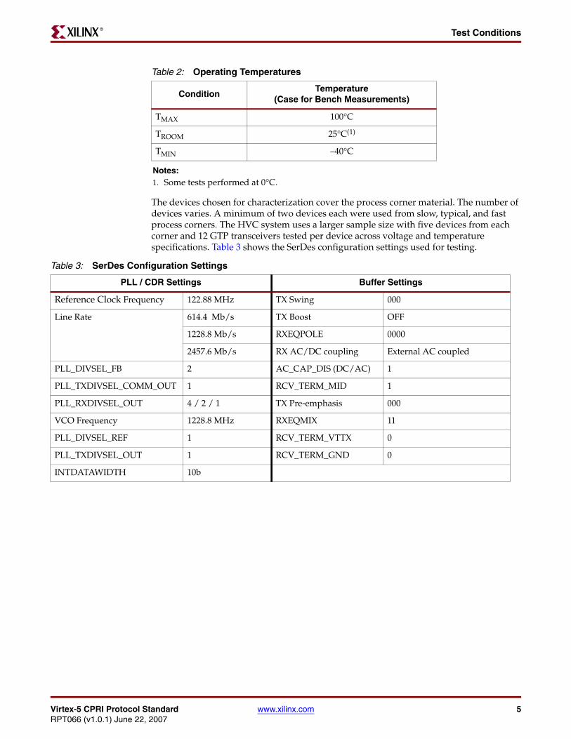
Test ConditionsTable 1 shows the operating supply voltages and Table 2 shows the operating temperatures.
Figure 1: CPRI System Diagram
TransmissionNetwork
TransmissionNetwork
Passive/ActiveElements
Passive/ActiveElements
TP2
TP3 TP4
TP1
Serdes
ConnectorConnector
Serdes
RPT066_01_011607
Table 1: Operating Supply Voltages
Condition MGTAVCC MGTAVCCPLL MGTAVTTRX MGTAVTTTX Units
VMIN 0.95 1.14V 1.14V 1.14V V
VNOM 1.0 1.20V 1.20V 1.20V V
VMAX 1.05 1.26V 1.26V 1.26V V
Notes: 1. Other FPGA voltages remain at nominal values.2. Some tests performed at ±10% VCC.
Virtex-5 CPRI Protocol Standard www.xilinx.com 5RPT066 (v1.0.1) June 22, 2007
Test ConditionsR
The devices chosen for characterization cover the process corner material. The number of devices varies. A minimum of two devices each were used from slow, typical, and fast process corners. The HVC system uses a larger sample size with five devices from each corner and 12 GTP transceivers tested per device across voltage and temperature specifications. Table 3 shows the SerDes configuration settings used for testing.
Table 2: Operating Temperatures
ConditionTemperature
(Case for Bench Measurements)
TMAX 100°C
TROOM 25°C(1)
TMIN –40°C
Notes: 1. Some tests performed at 0°C.
Table 3: SerDes Configuration Settings
PLL / CDR Settings Buffer Settings
Reference Clock Frequency 122.88 MHz TX Swing 000
Line Rate 614.4 Mb/s TX Boost OFF
1228.8 Mb/s RXEQPOLE 0000
2457.6 Mb/s RX AC/DC coupling External AC coupled
PLL_DIVSEL_FB 2 AC_CAP_DIS (DC/AC) 1
PLL_TXDIVSEL_COMM_OUT 1 RCV_TERM_MID 1
PLL_RXDIVSEL_OUT 4 / 2 / 1 TX Pre-emphasis 000
VCO Frequency 1228.8 MHz RXEQMIX 11
PLL_DIVSEL_REF 1 RCV_TERM_VTTX 0
PLL_TXDIVSEL_OUT 1 RCV_TERM_GND 0
INTDATAWIDTH 10b

6 www.xilinx.com Virtex-5 CPRI Protocol StandardRPT066 (v1.0.1) June 22, 2007
Summary of ResultsR
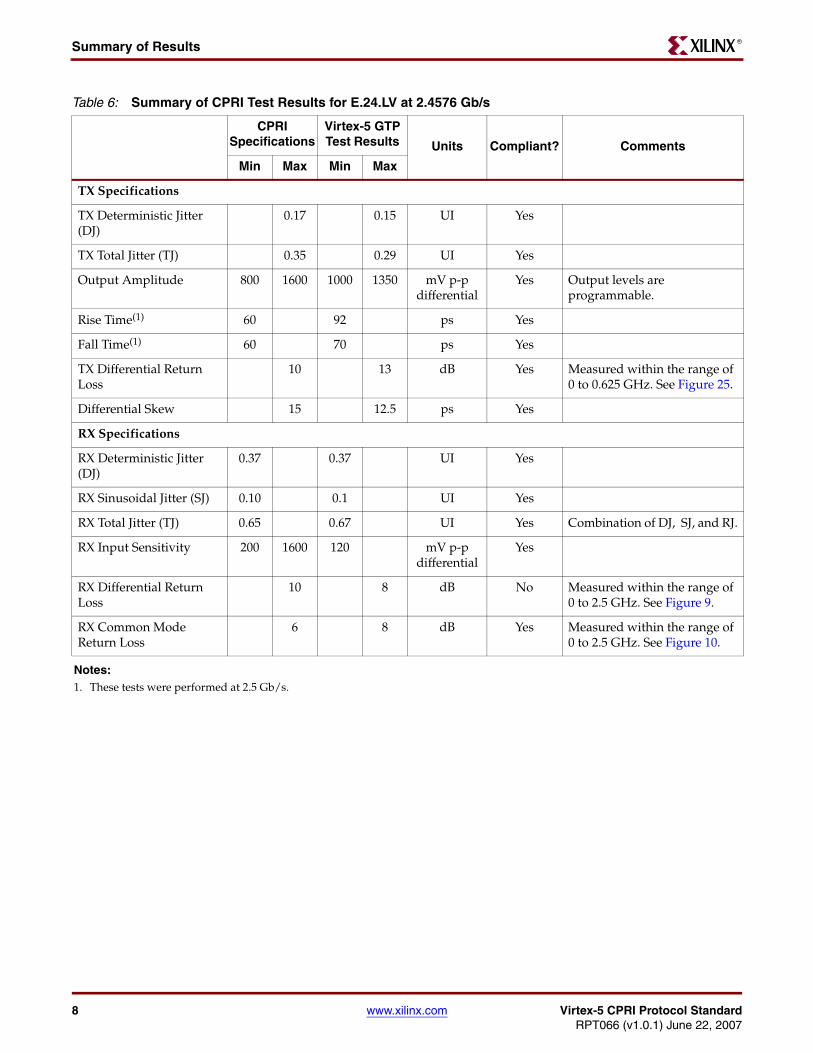
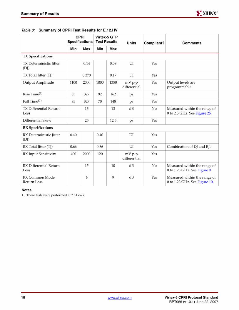
Summary of ResultsTable 4 through Table 8 are summary tables of the CPRI specification requirements and the test results for the Virtex-5 GTP transceiver.
Table 4: Summary of CPRI Test Results for E.6.LV at 614 Mb/s
CPRI Specifications
Virtex-5 GTP Test Results Units Compliant? Comments
Min Max Min Max
TX Specifications
TX Deterministic Jitter (DJ)
0.17 0.03 UI Yes
TX Total Jitter (TJ) 0.35 0.09 UI Yes
Output Amplitude(1) 800 1600 1000 1350 mV p-p differential
Yes Output levels are programmable.
Rise Time(1) 60 92 ps Yes
Fall Time(1) 60 70 ps Yes
TX Differential Return Loss
10 13 dB Yes Measured within the range of 0 to 0.625 GHz. See Figure 25.
Differential Skew 15 12.5 ps Yes
RX Specifications
RX Deterministic Jitter (DJ)
0.37 0.37 UI Yes
RX Sinusoidal Jitter (SJ) 0.10 0.15 UI Yes
RX Total Jitter (TJ) 0.65 0.7 UI Yes Combination of DJ, SJ, and RJ.
RX Input Sensitivity 200 1600 105 mV p-p differential
Yes
RX Differential Return Loss
10 10 dB Yes Measured within the range of 0 to 0.641 GHz. See Figure 9.
RX Common Mode Return Loss
6 10 dB Yes Measured within the range of 0 to 0.641 GHz. See Figure 10.
Notes: 1. These tests were performed at 2.5 Gb/s.

Virtex-5 CPRI Protocol Standard www.xilinx.com 7RPT066 (v1.0.1) June 22, 2007
Summary of ResultsR
Table 5: Summary of CPRI Test Results for E.12.LV at 1.2288 Gb/s
CPRI Specifications
Virtex-5 GTP Test Results Units Compliant? Comments
Min Max Min Max
TX Specifications
TX Deterministic Jitter (DJ)
0.17 0.09 UI Yes
TX Total Jitter (TJ) 0.35 0.17 UI Yes
Output Amplitude 800 1600 1000 1350 mV p-p differential
Yes Output levels are programmable.
Rise Time(1) 60 92 ps Yes
Fall Time(1) 60 70 ps Yes
TX Differential Return Loss
10 13 dB Yes Measured within the range of 0 to 0.625 GHz. See Figure 25.
Differential Skew 12.5 15 ps Yes
RX Specifications
RX Deterministic Jitter (DJ)
0.37 0.40 UI Yes
RX Sinusoidal Jitter (SJ) 0.10 0.1 UI Yes
RX Total Jitter (TJ) 0.65 0.76 UI Yes Combination of DJ, SJ, and RJ.
RX Input Sensitivity 200 1600 120 mV p-p differential
Yes
RX Differential Return Loss
10 10 dB Yes Measured within the range of 0 to 1.23 GHz. See Figure 9.
RX Common Mode Return Loss
6 9 dB Yes Measured within the range of 0 to 1.23 GHz. See Figure 10.
Notes: 1. These tests were performed at 2.5 Gb/s.
8 www.xilinx.com Virtex-5 CPRI Protocol StandardRPT066 (v1.0.1) June 22, 2007
Summary of ResultsR
Table 6: Summary of CPRI Test Results for E.24.LV at 2.4576 Gb/s
CPRI Specifications
Virtex-5 GTP Test Results Units Compliant? Comments
Min Max Min Max
TX Specifications
TX Deterministic Jitter (DJ)
0.17 0.15 UI Yes
TX Total Jitter (TJ) 0.35 0.29 UI Yes
Output Amplitude 800 1600 1000 1350 mV p-p differential
Yes Output levels are programmable.
Rise Time(1) 60 92 ps Yes
Fall Time(1) 60 70 ps Yes
TX Differential Return Loss
10 13 dB Yes Measured within the range of 0 to 0.625 GHz. See Figure 25.
Differential Skew 15 12.5 ps Yes
RX Specifications
RX Deterministic Jitter (DJ)
0.37 0.37 UI Yes
RX Sinusoidal Jitter (SJ) 0.10 0.1 UI Yes
RX Total Jitter (TJ) 0.65 0.67 UI Yes Combination of DJ, SJ, and RJ.
RX Input Sensitivity 200 1600 120 mV p-p differential
Yes
RX Differential Return Loss
10 8 dB No Measured within the range of 0 to 2.5 GHz. See Figure 9.
RX Common Mode Return Loss
6 8 dB Yes Measured within the range of 0 to 2.5 GHz. See Figure 10.
Notes: 1. These tests were performed at 2.5 Gb/s.

Virtex-5 CPRI Protocol Standard www.xilinx.com 9RPT066 (v1.0.1) June 22, 2007
Summary of ResultsR
Table 7: Summary of CPRI Test Results for E.6.HV
CPRI Specifications
Virtex-5 GTP Test Results Units Compliant? Comments
Min Max Min Max
TX Specifications
TX Deterministic Jitter (DJ)
0.14 0.03 UI Yes
TX Total Jitter (TJ) 0.279 0.09 UI Yes
Output Amplitude(1) 1100 2000 900 1100 mV p-p differential
Yes Output levels are programmable.
Rise Time(1) 85 327 92 ps Yes
Fall Time(1) 85 327 70 ps Yes
TX Differential Return Loss
15 13 dB No Measured within the range of 0 to 0.625 GHz. See Figure 25.
Differential Skew 25 12.5 ps Yes
RX Specifications
RX Deterministic Jitter (DJ)
0.40 0.40 UI Yes
RX Total Jitter (TJ) 0.66 0.69 UI Yes Combination of DJ and RJ.
RX Input Sensitivity 400 2000 105 mV p-p differential
Yes
RX Differential Return Loss
15 10 dB No Measured within the range of 0 to 0.641 GHz. See Figure 9.
RX Common Mode Return Loss
6 10 dB Yes Measured within the range of 0 to 0.641 GHz. See Figure 10.
Notes: 1. These tests were performed at 2.5 Gb/s.
10 www.xilinx.com Virtex-5 CPRI Protocol StandardRPT066 (v1.0.1) June 22, 2007
Summary of ResultsR
Table 8: Summary of CPRI Test Results for E.12.HV
CPRI Specifications
Virtex-5 GTP Test Results Units Compliant? Comments
Min Max Min Max
TX Specifications
TX Deterministic Jitter (DJ)
0.14 0.09 UI Yes
TX Total Jitter (TJ) 0.279 0.17 UI Yes
Output Amplitude 1100 2000 1000 1350 mV p-p differential
Yes Output levels are programmable.
Rise Time(1) 85 327 92 162 ps Yes
Fall Time(1) 85 327 70 148 ps Yes
TX Differential Return Loss
15 13 dB No Measured within the range of 0 to 2.5 GHz. See Figure 25.
Differential Skew 25 12.5 ps Yes
RX Specifications
RX Deterministic Jitter (DJ)
0.40 0.40 UI Yes
RX Total Jitter (TJ) 0.66 0.66 UI Yes Combination of DJ and RJ.
RX Input Sensitivity 400 2000 120 mV p-p differential
Yes
RX Differential Return Loss
15 10 dB No Measured within the range of 0 to 1.23 GHz. See Figure 9.
RX Common Mode Return Loss
6 9 dB Yes Measured within the range of 0 to 1.23 GHz. See Figure 10.
Notes: 1. These tests were performed at 2.5 Gb/s.
Virtex-5 CPRI Protocol Standard www.xilinx.com 11RPT066 (v1.0.1) June 22, 2007
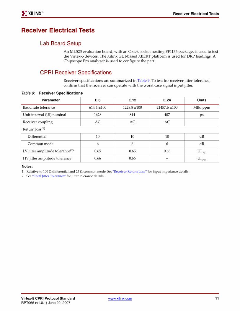
Receiver Electrical TestsR
Receiver Electrical Tests
Lab Board SetupAn ML523 evaluation board, with an Oztek socket hosting FF1136 package, is used to test the Virtex-5 devices. The Xilinx GUI-based XBERT platform is used for DRP loadings. A Chipscope Pro analyzer is used to configure the part.
CPRI Receiver SpecificationsReceiver specifications are summarized in Table 9. To test for receiver jitter tolerance, confirm that the receiver can operate with the worst case signal input jitter.
Table 9: Receiver Specifications
Parameter E.6 E.12 E.24 Units
Baud rate tolerance 614.4 ±100 1228.8 ±100 21457.6 ±100 MBd ppm
Unit interval (UI) nominal 1628 814 407 ps
Receiver coupling AC AC AC
Return loss(1)
Differential 10 10 10 dB
Common mode 6 6 6 dB
LV jitter amplitude tolerance(2) 0.65 0.65 0.65 UIp-p
HV jitter amplitude tolerance 0.66 0.66 – UIp-p
Notes: 1. Relative to 100 Ω differential and 25 Ω common mode. See“Receiver Return Loss” for input impedance details.2. See “Total Jitter Tolerance” for jitter tolerance details.
12 www.xilinx.com Virtex-5 CPRI Protocol StandardRPT066 (v1.0.1) June 22, 2007
Receiver Electrical TestsR
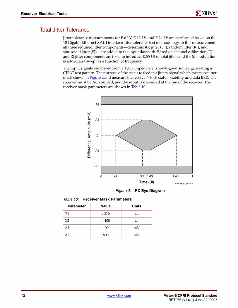
Total Jitter ToleranceJitter tolerance measurements for E.6.LV, E.12.LV, and E.24.LV are performed based on the 10 Gigabit Ethernet XAUI interface jitter tolerance test methodology. In this measurement, all three required jitter components—deterministic jitter (DJ), random jitter (RJ), and sinusoidal jitter (SJ)—are added to the input datapath. Based on channel calibration, DJ and RJ jitter components are fixed to introduce 0.55 UI of total jitter, and the SJ modulation is added and swept as a function of frequency.
The input signals are driven from a 100Ω impedance, known-good source generating a CJPAT test pattern. The purpose of the test is to feed in a jittery signal which meets the jitter mask shown in Figure 2 and measure the receiver's lock status, stability, and data BER. The receiver must be AC coupled, and the input is measured at the pin of the receiver. The receiver mask parameters are shown in Table 10.
Figure 2: RX Eye Diagram
Table 10: Receiver Mask Parameters
Parameter Value Units
X1 0.275 UI
X2 0.400 UI
A1 100 mV
A2 800 mV
0
–A1
A1
A2
–A2
0 1-X1X1 1
Time (UI)
X2 1-X2
Diff
eren
tial A
mpl
itude
(m
V)
RPT066_02_011607
Virtex-5 CPRI Protocol Standard www.xilinx.com 13RPT066 (v1.0.1) June 22, 2007
Receiver Electrical TestsR
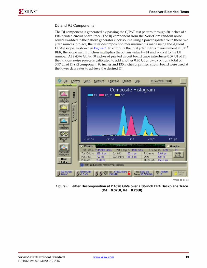
DJ and RJ Components
The DJ component is generated by passing the CJPAT test pattern through 50 inches of a FR4 printed circuit board trace. The RJ component from the NoiseCom random noise source is added to the pattern generator clock source using a power splitter. With these two jitter sources in place, the jitter decomposition measurement is made using the Agilent DCA-J scope, as shown in Figure 3. To compute the total jitter in this measurement at 10-12 BER, the scope math function multiplies the RJ rms value by 14 and adds it to the DJ number. At 2.4576 Gb/s, 50 inches of printed circuit board trace introduces 0.37 UI of DJ, the random noise source is calibrated to add another 0.20 UI of pk-pk RJ for a total of 0.57 UI of DJ+RJ component. 90 inches and 135 inches of printed circuit board were used at the lower data rates to achieve the desired DJ.
Figure 3: Jitter Decomposition at 2.4576 Gb/s over a 50-inch FR4 Backplane Trace (DJ = 0.37UI, RJ = 0.20UI)
RPT066_03_011603
14 www.xilinx.com Virtex-5 CPRI Protocol StandardRPT066 (v1.0.1) June 22, 2007
Receiver Electrical TestsR
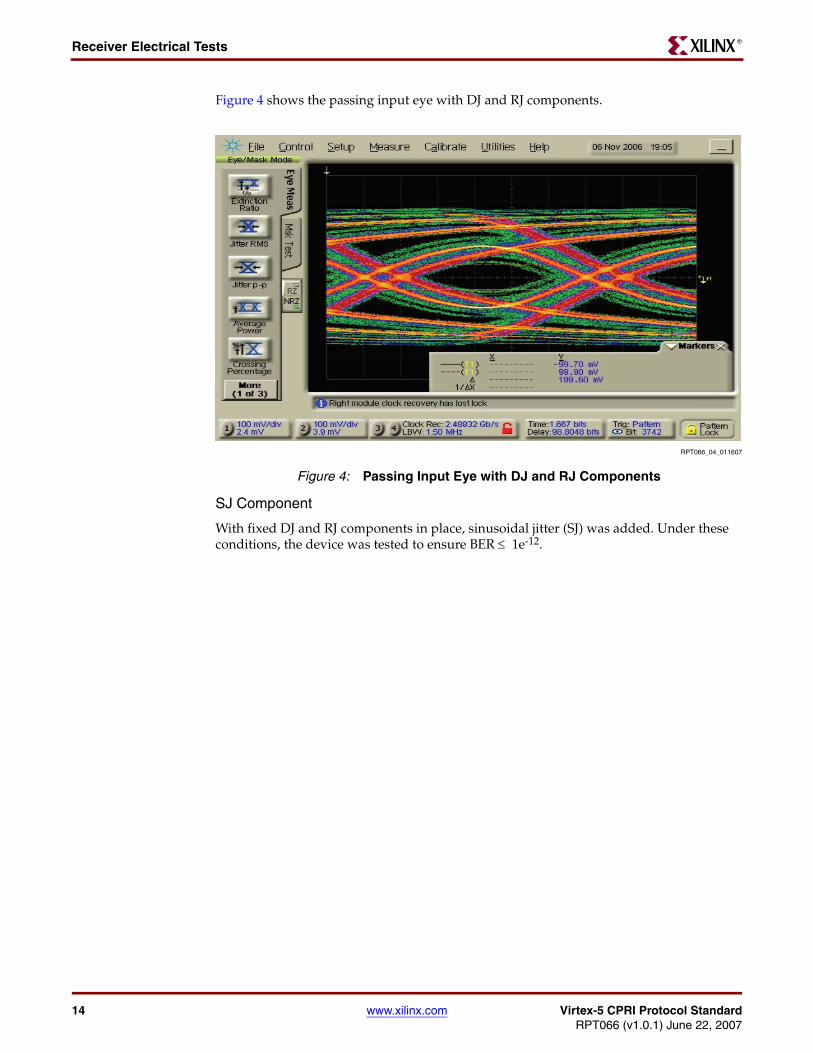
Figure 4 shows the passing input eye with DJ and RJ components.
SJ Component
With fixed DJ and RJ components in place, sinusoidal jitter (SJ) was added. Under these conditions, the device was tested to ensure BER ≤ 1e-12.
Figure 4: Passing Input Eye with DJ and RJ Components
RPT066_04_011607
Virtex-5 CPRI Protocol Standard www.xilinx.com 15RPT066 (v1.0.1) June 22, 2007
Receiver Electrical TestsR
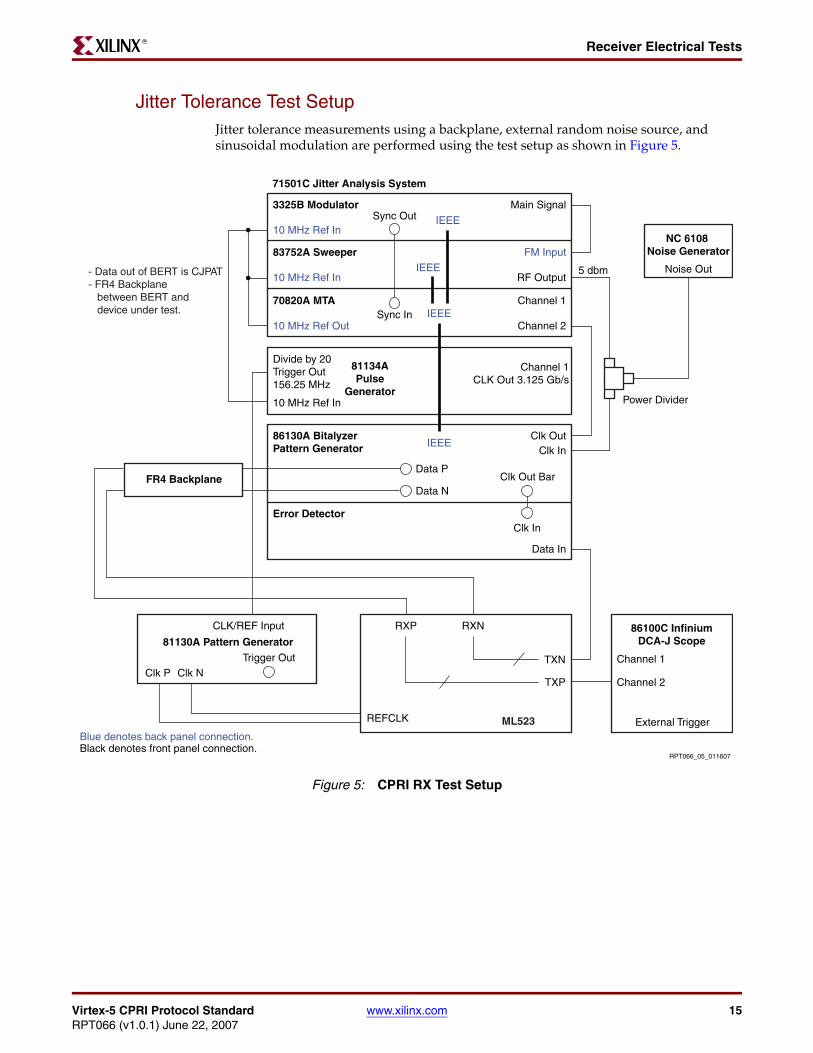
Jitter Tolerance Test SetupJitter tolerance measurements using a backplane, external random noise source, and sinusoidal modulation are performed using the test setup as shown in Figure 5.
Figure 5: CPRI RX Test Setup
Main Signal
NC 6108 Noise Generator
Noise Out
3325B ModulatorSync Out
Sync In
10 MHz Ref In
FM Input
IEEE
IEEE
IEEE
IEEE
83752A Sweeper
10 MHz Ref In RF Output5 dbm
Power Divider
Channel 170820A MTA
10 MHz Ref Out Channel 2
Clk InError Detector
86100C InfiniumDCA-J Scope
ML523
81130A Pattern Generator
81134APulse
Generator
Data In
Clk Out
Clk Out Bar
86130A BitalyzerPattern Generator
FR4 Backplane
Clk In
Data P
Data N
RXP RXN
TXN
TXP Channel 2
External Trigger
Channel 1
Channel 1CLK Out 3.125 Gb/s
Divide by 20Trigger Out156.25 MHz
10 MHz Ref In
Clk P Clk N
CLK/REF Input
Trigger Out
REFCLK
Blue denotes back panel connection.Black denotes front panel connection.
RPT066_05_011607
- Data out of BERT is CJPAT- FR4 Backplane between BERT and device under test.
71501C Jitter Analysis System
16 www.xilinx.com Virtex-5 CPRI Protocol StandardRPT066 (v1.0.1) June 22, 2007
Receiver Electrical TestsR
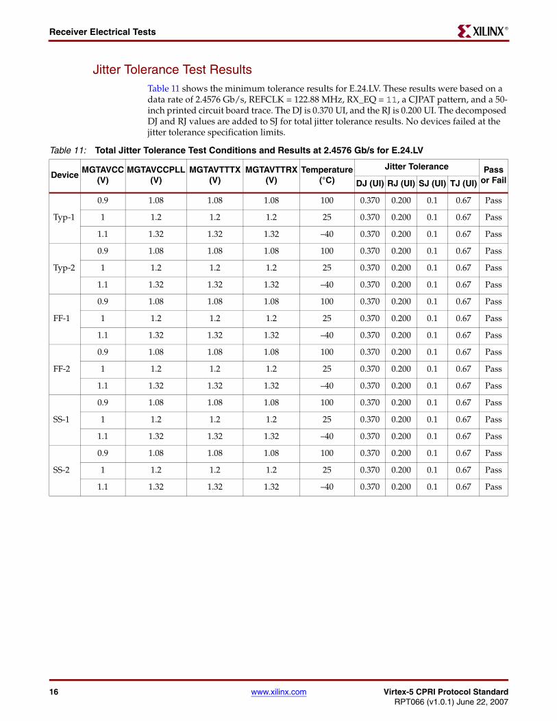
Jitter Tolerance Test ResultsTable 11 shows the minimum tolerance results for E.24.LV. These results were based on a data rate of 2.4576 Gb/s, REFCLK = 122.88 MHz, RX_EQ = 11, a CJPAT pattern, and a 50-inch printed circuit board trace. The DJ is 0.370 UI, and the RJ is 0.200 UI. The decomposed DJ and RJ values are added to SJ for total jitter tolerance results. No devices failed at the jitter tolerance specification limits.
Table 11: Total Jitter Tolerance Test Conditions and Results at 2.4576 Gb/s for E.24.LV
DeviceMGTAVCC
(V)MGTAVCCPLL
(V)MGTAVTTTX
(V)MGTAVTTRX
(V)Temperature
(°C)
Jitter Tolerance Pass or FailDJ (UI) RJ (UI) SJ (UI) TJ (UI)
Typ-1
0.9 1.08 1.08 1.08 100 0.370 0.200 0.1 0.67 Pass
1 1.2 1.2 1.2 25 0.370 0.200 0.1 0.67 Pass
1.1 1.32 1.32 1.32 –40 0.370 0.200 0.1 0.67 Pass
Typ-2
0.9 1.08 1.08 1.08 100 0.370 0.200 0.1 0.67 Pass
1 1.2 1.2 1.2 25 0.370 0.200 0.1 0.67 Pass
1.1 1.32 1.32 1.32 –40 0.370 0.200 0.1 0.67 Pass
FF-1
0.9 1.08 1.08 1.08 100 0.370 0.200 0.1 0.67 Pass
1 1.2 1.2 1.2 25 0.370 0.200 0.1 0.67 Pass
1.1 1.32 1.32 1.32 –40 0.370 0.200 0.1 0.67 Pass
FF-2
0.9 1.08 1.08 1.08 100 0.370 0.200 0.1 0.67 Pass
1 1.2 1.2 1.2 25 0.370 0.200 0.1 0.67 Pass
1.1 1.32 1.32 1.32 –40 0.370 0.200 0.1 0.67 Pass
SS-1
0.9 1.08 1.08 1.08 100 0.370 0.200 0.1 0.67 Pass
1 1.2 1.2 1.2 25 0.370 0.200 0.1 0.67 Pass
1.1 1.32 1.32 1.32 –40 0.370 0.200 0.1 0.67 Pass
SS-2
0.9 1.08 1.08 1.08 100 0.370 0.200 0.1 0.67 Pass
1 1.2 1.2 1.2 25 0.370 0.200 0.1 0.67 Pass
1.1 1.32 1.32 1.32 –40 0.370 0.200 0.1 0.67 Pass

Virtex-5 CPRI Protocol Standard www.xilinx.com 17RPT066 (v1.0.1) June 22, 2007
Receiver Electrical TestsR
Table 12 shows the minimum tolerance results for E.12.HV. These results were based on a data rate of 1.2288 Gb/s, REFCLK = 122.88 MHz. RX_EQ = 11, a CJPAT test pattern, and a 90-inch backplane. The DJ is 0.4 UI and the RJ is 0.26 UI. No devices failed at the jitter tolerance specification limit.
Table 12: Total Jitter Tolerance Test Conditions and Results at 1.2288 Gb/s for E.12.HV
DeviceMGTAVCC
(V)MGTAVCCPLL
(V)MGTAVTTTX
(V)MGTAVTTRX
(V)Temperature
(°C)
Jitter Tolerance Error Free(Min)
Pass or FailDJ (UI) RJ (UI) TJ (UI)
Typ-1
0.9 1.08 1.08 1.08 100 0.4 0.26 0.66 15 Pass
1 1.2 1.2 1.2 25 0.4 0.26 0.66 15 Pass
1.1 1.32 1.32 1.32 –40 0.4 0.26 0.66 15 Pass
Typ-2
0.9 1.08 1.08 1.08 100 0.4 0.26 0.66 15 Pass
1 1.2 1.2 1.2 25 0.4 0.26 0.66 15 Pass
1.1 1.32 1.32 1.32 –40 0.4 0.26 0.66 15 Pass
FF-1
0.9 1.08 1.08 1.08 100 0.4 0.26 0.66 15 Pass
1 1.2 1.2 1.2 25 0.4 0.26 0.66 15 Pass
1.1 1.32 1.32 1.32 –40 0.4 0.26 0.66 15 Pass
FF-2
0.9 1.08 1.08 1.08 100 0.4 0.26 0.66 15 Pass
1 1.2 1.2 1.2 25 0.4 0.26 0.66 15 Pass
1.1 1.32 1.32 1.32 –40 0.4 0.26 0.66 15 Pass
SS-1
0.9 1.08 1.08 1.08 100 0.4 0.26 0.66 15 Pass
1 1.2 1.2 1.2 25 0.4 0.26 0.66 15 Pass
1.1 1.32 1.32 1.32 –40 0.4 0.26 0.66 15 Pass
SS-2
0.9 1.08 1.08 1.08 100 0.4 0.26 0.66 15 Pass
1 1.2 1.2 1.2 25 0.4 0.26 0.66 15 Pass
1.1 1.32 1.32 1.32 –40 0.4 0.26 0.66 15 Pass
18 www.xilinx.com Virtex-5 CPRI Protocol StandardRPT066 (v1.0.1) June 22, 2007
Receiver Electrical TestsR
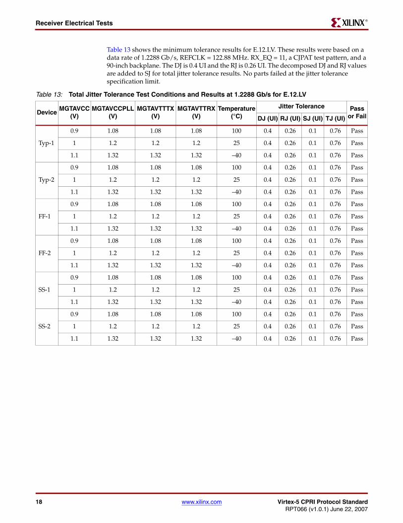
Table 13 shows the minimum tolerance results for E.12.LV. These results were based on a data rate of 1.2288 Gb/s, REFCLK = 122.88 MHz. RX_EQ = 11, a CJPAT test pattern, and a 90-inch backplane. The DJ is 0.4 UI and the RJ is 0.26 UI. The decomposed DJ and RJ values are added to SJ for total jitter tolerance results. No parts failed at the jitter tolerance specification limit.
Table 13: Total Jitter Tolerance Test Conditions and Results at 1.2288 Gb/s for E.12.LV
DeviceMGTAVCC
(V)MGTAVCCPLL
(V)MGTAVTTTX
(V)MGTAVTTRX
(V)Temperature
(°C)
Jitter Tolerance Pass or FailDJ (UI) RJ (UI) SJ (UI) TJ (UI)
Typ-1
0.9 1.08 1.08 1.08 100 0.4 0.26 0.1 0.76 Pass
1 1.2 1.2 1.2 25 0.4 0.26 0.1 0.76 Pass
1.1 1.32 1.32 1.32 –40 0.4 0.26 0.1 0.76 Pass
Typ-2
0.9 1.08 1.08 1.08 100 0.4 0.26 0.1 0.76 Pass
1 1.2 1.2 1.2 25 0.4 0.26 0.1 0.76 Pass
1.1 1.32 1.32 1.32 –40 0.4 0.26 0.1 0.76 Pass
FF-1
0.9 1.08 1.08 1.08 100 0.4 0.26 0.1 0.76 Pass
1 1.2 1.2 1.2 25 0.4 0.26 0.1 0.76 Pass
1.1 1.32 1.32 1.32 –40 0.4 0.26 0.1 0.76 Pass
FF-2
0.9 1.08 1.08 1.08 100 0.4 0.26 0.1 0.76 Pass
1 1.2 1.2 1.2 25 0.4 0.26 0.1 0.76 Pass
1.1 1.32 1.32 1.32 –40 0.4 0.26 0.1 0.76 Pass
SS-1
0.9 1.08 1.08 1.08 100 0.4 0.26 0.1 0.76 Pass
1 1.2 1.2 1.2 25 0.4 0.26 0.1 0.76 Pass
1.1 1.32 1.32 1.32 –40 0.4 0.26 0.1 0.76 Pass
SS-2
0.9 1.08 1.08 1.08 100 0.4 0.26 0.1 0.76 Pass
1 1.2 1.2 1.2 25 0.4 0.26 0.1 0.76 Pass
1.1 1.32 1.32 1.32 –40 0.4 0.26 0.1 0.76 Pass
Virtex-5 CPRI Protocol Standard www.xilinx.com 19RPT066 (v1.0.1) June 22, 2007
Receiver Electrical TestsR
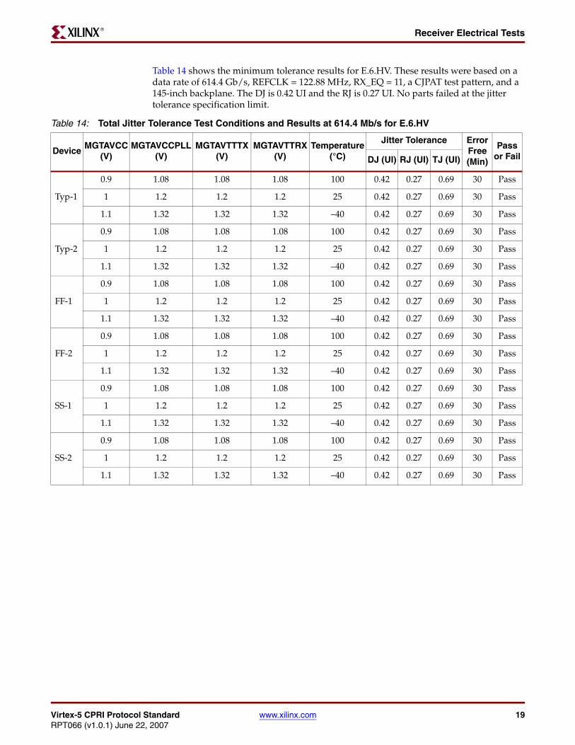
Table 14 shows the minimum tolerance results for E.6.HV. These results were based on a data rate of 614.4 Gb/s, REFCLK = 122.88 MHz, RX_EQ = 11, a CJPAT test pattern, and a 145-inch backplane. The DJ is 0.42 UI and the RJ is 0.27 UI. No parts failed at the jitter tolerance specification limit.
Table 14: Total Jitter Tolerance Test Conditions and Results at 614.4 Mb/s for E.6.HV
DeviceMGTAVCC
(V)MGTAVCCPLL
(V)MGTAVTTTX
(V)MGTAVTTRX
(V)Temperature
(°C)
Jitter Tolerance Error Free(Min)
Pass or FailDJ (UI) RJ (UI) TJ (UI)
Typ-1
0.9 1.08 1.08 1.08 100 0.42 0.27 0.69 30 Pass
1 1.2 1.2 1.2 25 0.42 0.27 0.69 30 Pass
1.1 1.32 1.32 1.32 –40 0.42 0.27 0.69 30 Pass
Typ-2
0.9 1.08 1.08 1.08 100 0.42 0.27 0.69 30 Pass
1 1.2 1.2 1.2 25 0.42 0.27 0.69 30 Pass
1.1 1.32 1.32 1.32 –40 0.42 0.27 0.69 30 Pass
FF-1
0.9 1.08 1.08 1.08 100 0.42 0.27 0.69 30 Pass
1 1.2 1.2 1.2 25 0.42 0.27 0.69 30 Pass
1.1 1.32 1.32 1.32 –40 0.42 0.27 0.69 30 Pass
FF-2
0.9 1.08 1.08 1.08 100 0.42 0.27 0.69 30 Pass
1 1.2 1.2 1.2 25 0.42 0.27 0.69 30 Pass
1.1 1.32 1.32 1.32 –40 0.42 0.27 0.69 30 Pass
SS-1
0.9 1.08 1.08 1.08 100 0.42 0.27 0.69 30 Pass
1 1.2 1.2 1.2 25 0.42 0.27 0.69 30 Pass
1.1 1.32 1.32 1.32 –40 0.42 0.27 0.69 30 Pass
SS-2
0.9 1.08 1.08 1.08 100 0.42 0.27 0.69 30 Pass
1 1.2 1.2 1.2 25 0.42 0.27 0.69 30 Pass
1.1 1.32 1.32 1.32 –40 0.42 0.27 0.69 30 Pass

20 www.xilinx.com Virtex-5 CPRI Protocol StandardRPT066 (v1.0.1) June 22, 2007
Receiver Electrical TestsR
Table 15 shows the minimum tolerance results for E.6.LV. These results were based on a data rate of 614.4 Mb/s, REFCLK = 122.88 MHz, RX_EQ = 11, a CJPAT test pattern, and a 135-inch backplane. The DJ is 0.37 UI and the RJ is 0.18 UI. The decomposed DJ and RJ values are added to SJ for total jitter tolerance results. No parts failed at the jitter tolerance specification limit.
Receiver Input SensitivityThe receiver differential amplitude test measures the minimum differential voltage amplitude between the positive and negative receiver pins with error free operation of the GTP receivers for the duration of the 0.5s test period. The input signals are to be driven from a 100Ω impedance, known-good source.
Test SetupA variable input voltage is applied to the DUT RX from the Agilent ParBERT pattern generator, and a BER test is performed. RX input sensitivity is defined as the last passing voltage.
Table 15: Total Jitter Tolerance Test Conditions and Results at 614.4 Mb/s for E.6.LV
DeviceMGTAVCC
(V)MGTAVCCPLL
(V)MGTAVTTTX
(V)MGTAVTTRX
(V)Temperature
(°C)
Jitter Tolerance Pass or FailDJ (UI) RJ (UI) SJ (UI) TJ (UI)
Typ-1
0.9 1.08 1.08 1.08 100 0.37 0.18 0.15 0.7 Pass
1 1.2 1.2 1.2 25 0.37 0.18 0.15 0.7 Pass
1.1 1.32 1.32 1.32 –40 0.37 0.18 0.15 0.7 Pass
Typ-2
0.9 1.08 1.08 1.08 100 0.37 0.18 0.15 0.7 Pass
1 1.2 1.2 1.2 25 0.37 0.18 0.15 0.7 Pass
1.1 1.32 1.32 1.32 –40 0.37 0.18 0.15 0.7 Pass
FF-1
0.9 1.08 1.08 1.08 100 0.37 0.18 0.15 0.7 Pass
1 1.2 1.2 1.2 25 0.37 0.18 0.15 0.7 Pass
1.1 1.32 1.32 1.32 –40 0.37 0.18 0.15 0.7 Pass
FF-2
0.9 1.08 1.08 1.08 100 0.37 0.18 0.15 0.7 Pass
1 1.2 1.2 1.2 25 0.37 0.18 0.15 0.7 Pass
1.1 1.32 1.32 1.32 –40 0.37 0.18 0.15 0.7 Pass
SS-1
0.9 1.08 1.08 1.08 100 0.37 0.18 0.15 0.7 Pass
1 1.2 1.2 1.2 25 0.37 0.18 0.15 0.7 Pass
1.1 1.32 1.32 1.32 –40 0.37 0.18 0.15 0.7 Pass
SS-2
0.9 1.08 1.08 1.08 100 0.37 0.18 0.15 0.7 Pass
1 1.2 1.2 1.2 25 0.37 0.18 0.15 0.7 Pass
1.1 1.32 1.32 1.32 –40 0.37 0.18 0.15 0.7 Pass
Virtex-5 CPRI Protocol Standard www.xilinx.com 21RPT066 (v1.0.1) June 22, 2007
Receiver Electrical TestsR
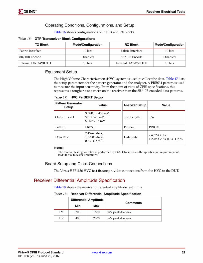
Operating Conditions, Configurations, and Setup
Table 16 shows configurations of the TX and RX blocks.
Equipment Setup
The High Volume Characterization (HVC) system is used to collect the data. Table 17 lists the setup parameters for the pattern generator and the analyzer. A PRBS31 pattern is used to measure the input sensitivity. From the point of view of CPRI specifications, this represents a tougher test pattern on the receiver than the 8B/10B encoded data patterns.
Board Setup and Clock Connections
The Virtex-5 FF1136 HVC test fixture provides connections from the HVC to the DUT.
Receiver Differential Amplitude SpecificationTable 18 shows the receiver differential amplitude test limits.
Table 16: GTP Transceiver Block Configurations
TX Block Mode/Configuration RX Block Mode/Configuration
Fabric Interface 10 bits Fabric Interface 10 bits
8B/10B Encode Disabled 8B/10B Encode Disabled
Internal DATAWIDTH 10 bits Internal DATAWIDTH 10 bits
Table 17: HVC ParBERT Setup
Pattern Generator Setup
Value Analyzer Setup Value
Output LevelSTART = 400 mV, STOP = 0 mV, STEP = 15 mV
Test Length 0.5s
Pattern PRBS31 Pattern PRBS31
Data Rate2.4576 Gb/s, 1.2288 Gb/s, 0.630 Gb/s(1)
Data Rate2.4576 Gb/s, 1.2288 Gb/s, 0.630 Gb/s
Notes: 1. The receiver testing for E.6 was performed at 0.630 Gb/s (versus the specification requirement of
0.6144) due to tester limitations.
Table 18: Receiver Differential Amplitude Specification
Differential AmplitudeComments
Min Max
LV 200 1600 mV peak-to-peak
HV 400 2000 mV peak-to-peak
22 www.xilinx.com Virtex-5 CPRI Protocol StandardRPT066 (v1.0.1) June 22, 2007
Receiver Electrical TestsR
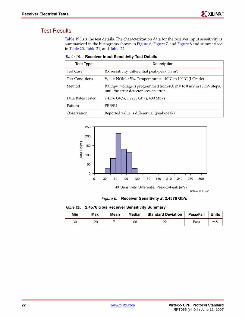
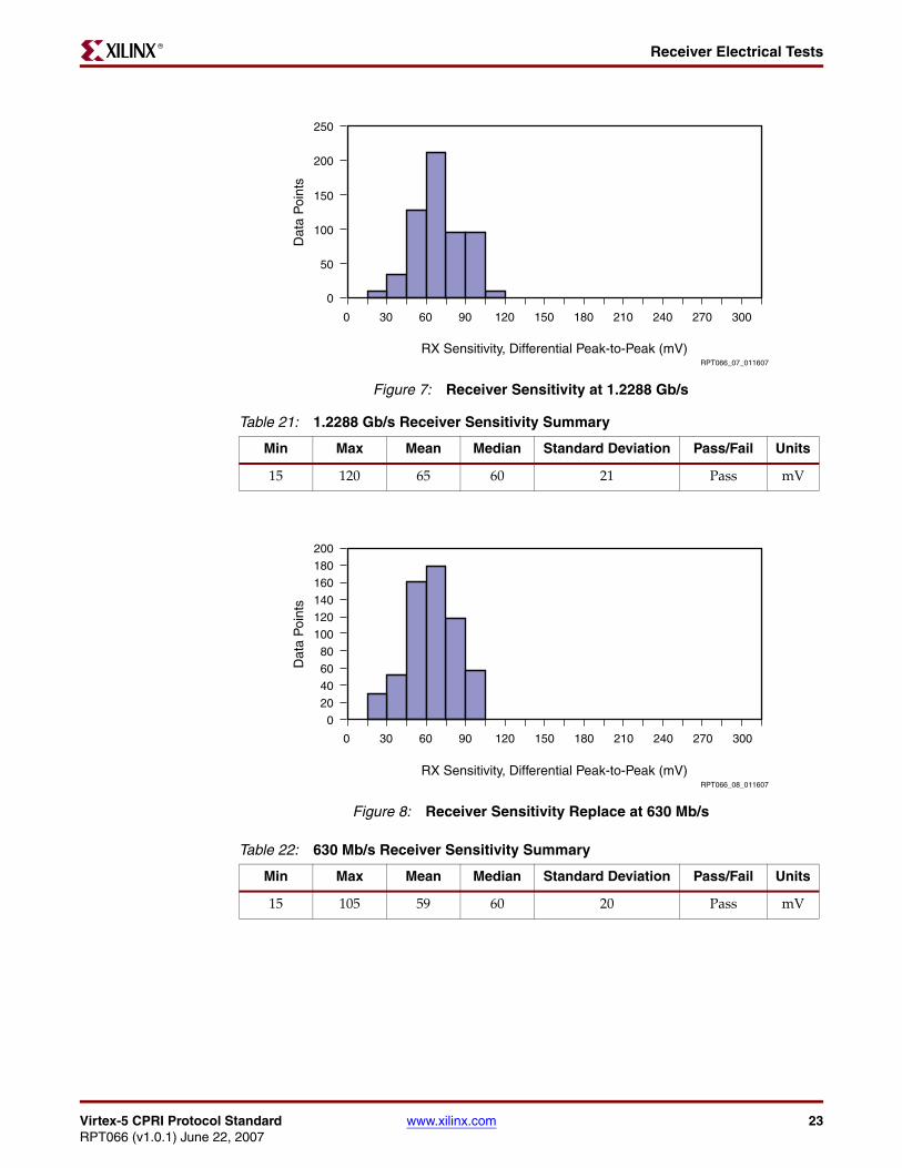
Test ResultsTable 19 lists the test details. The characterization data for the receiver input sensitivity is summarized in the histograms shown in Figure 6, Figure 7, and Figure 8 and summarized in Table 20, Table 21, and Table 22.
Table 19: Receiver Input Sensitivity Test Details
Test Type Description
Test Case RX sensitivity, differential peak-peak, in mV
Test Conditions VCC = NOM, ±5%, Temperature = –40°C to 100°C (I-Grade)
Method RX input voltage is programmed from 400 mV to 0 mV in 15 mV steps, until the error detector sees an error.
Data Rates Tested 2.4576 Gb/s, 1.2288 Gb/s, 630 Mb/s
Pattern PRBS31
Observation Reported value is differential (peak-peak)
Figure 6: Receiver Sensitivity at 2.4576 Gb/s
Table 20: 2.4576 Gb/s Receiver Sensitivity Summary
Min Max Mean Median Standard Deviation Pass/Fail Units
30 120 71 60 22 Pass mV
200
150
100
50
250
0
0 30 60 90 120 150 210 240 270 300180
RX Sensitivity, Differential Peak-to-Peak (mV)
Dat
a P
oint
s
RPT066_06_011607
Virtex-5 CPRI Protocol Standard www.xilinx.com 23RPT066 (v1.0.1) June 22, 2007
Receiver Electrical TestsR
Figure 7: Receiver Sensitivity at 1.2288 Gb/s
Table 21: 1.2288 Gb/s Receiver Sensitivity Summary
Min Max Mean Median Standard Deviation Pass/Fail Units
15 120 65 60 21 Pass mV
Figure 8: Receiver Sensitivity Replace at 630 Mb/s
Table 22: 630 Mb/s Receiver Sensitivity Summary
Min Max Mean Median Standard Deviation Pass/Fail Units
15 105 59 60 20 Pass mV
200
150
100
50
250
0
0 30 60 90 120 150 210 240 270 300180
RX Sensitivity, Differential Peak-to-Peak (mV)
Dat
a P
oint
s
RPT066_07_011607
200
180
160
140
120
100
80
60
40
20
0
0 30 60 90 120 150 210 240 270 300180
RX Sensitivity, Differential Peak-to-Peak (mV)
Dat
a P
oint
s
RPT066_08_011607

24 www.xilinx.com Virtex-5 CPRI Protocol StandardRPT066 (v1.0.1) June 22, 2007
Receiver Electrical TestsR
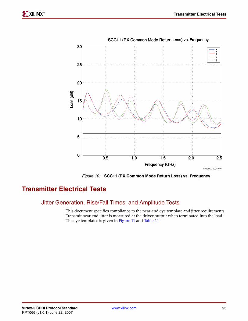
Receiver Return LossThe receiver input should have a differential return loss better than 10 dB for the LV variants and better than 15 dB for the HV variants. The common mode return loss should be better than 6 dB for both variants. The maximum measurement frequency is the baud rate of the variant (that is 0.6144 GHz for E.6.) This includes contributions from on-chip circuitry, the chip package, and any off-chip components related to the receiver. AC coupling components are included in this requirement. The reference impedance for return loss measurements is 100Ω for differential return loss and 25Ω for common mode.
The frequency domain return loss measurements (Figure 9 and Figure 10) were made using the UNH inter-operability lab guidelines. The four traces represent different GTP receivers with varying PCB trace lengths. The common mode return loss is within the requirements of the CPRI specifications. The return loss measurements based on the UNH inter-operability labs testing show a differential return loss of 8 dB at 2.5 GHz.
Higher return loss values (more positive) increase the amount of reflections back to the transmitter resulting in more inter-symbol interference (ISI). The GTP receiver equalization circuits can mitigate the effects of eye closure due to the reflection. The UNH inter-operability lab testing showed no increase in receiver BER due to the receiver differential return loss.
Figure 9: SDD11 (RX Differential Return Loss) vs. Frequency
RPT066_09_011607
Virtex-5 CPRI Protocol Standard www.xilinx.com 25RPT066 (v1.0.1) June 22, 2007
Transmitter Electrical TestsR
Transmitter Electrical Tests
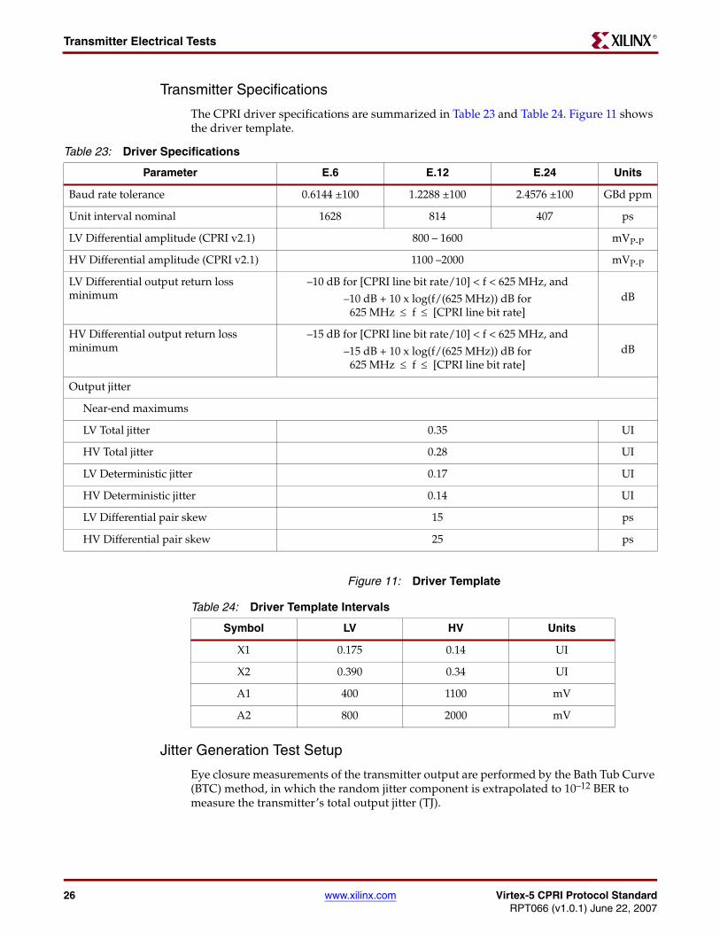
Jitter Generation, Rise/Fall Times, and Amplitude TestsThis document specifies compliance to the near-end eye template and jitter requirements. Transmit near-end jitter is measured at the driver output when terminated into the load. The eye templates is given in Figure 11 and Table 24.
Figure 10: SCC11 (RX Common Mode Return Loss) vs. Frequency
RPT066_10_011607
26 www.xilinx.com Virtex-5 CPRI Protocol StandardRPT066 (v1.0.1) June 22, 2007
Transmitter Electrical TestsR
Transmitter Specifications
The CPRI driver specifications are summarized in Table 23 and Table 24. Figure 11 shows the driver template.
Jitter Generation Test Setup
Eye closure measurements of the transmitter output are performed by the Bath Tub Curve (BTC) method, in which the random jitter component is extrapolated to 10–12 BER to measure the transmitter’s total output jitter (TJ).
Table 23: Driver Specifications
Parameter E.6 E.12 E.24 Units
Baud rate tolerance 0.6144 ±100 1.2288 ±100 2.4576 ±100 GBd ppm
Unit interval nominal 1628 814 407 ps
LV Differential amplitude (CPRI v2.1) 800 – 1600 mVP-P
HV Differential amplitude (CPRI v2.1) 1100 –2000 mVP-P
LV Differential output return loss minimum
–10 dB for [CPRI line bit rate/10] < f < 625 MHz, and
–10 dB + 10 x log(f/(625 MHz)) dB for 625 MHz ≤ f ≤ [CPRI line bit rate]
dB
HV Differential output return loss minimum
–15 dB for [CPRI line bit rate/10] < f < 625 MHz, and
–15 dB + 10 x log(f/(625 MHz)) dB for 625 MHz ≤ f ≤ [CPRI line bit rate]
dB
Output jitter
Near-end maximums
LV Total jitter 0.35 UI
HV Total jitter 0.28 UI
LV Deterministic jitter 0.17 UI
HV Deterministic jitter 0.14 UI
LV Differential pair skew 15 ps
HV Differential pair skew 25 ps
Figure 11: Driver Template
Table 24: Driver Template Intervals
Symbol LV HV Units
X1 0.175 0.14 UI
X2 0.390 0.34 UI
A1 400 1100 mV
A2 800 2000 mV
Virtex-5 CPRI Protocol Standard www.xilinx.com 27RPT066 (v1.0.1) June 22, 2007
Transmitter Electrical TestsR
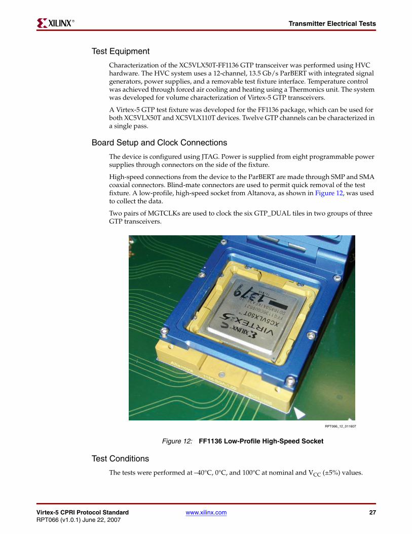
Test Equipment
Characterization of the XC5VLX50T-FF1136 GTP transceiver was performed using HVC hardware. The HVC system uses a 12-channel, 13.5 Gb/s ParBERT with integrated signal generators, power supplies, and a removable test fixture interface. Temperature control was achieved through forced air cooling and heating using a Thermonics unit. The system was developed for volume characterization of Virtex-5 GTP transceivers.
A Virtex-5 GTP test fixture was developed for the FF1136 package, which can be used for both XC5VLX50T and XC5VLX110T devices. Twelve GTP channels can be characterized in a single pass.
Board Setup and Clock Connections
The device is configured using JTAG. Power is supplied from eight programmable power supplies through connectors on the side of the fixture.
High-speed connections from the device to the ParBERT are made through SMP and SMA coaxial connectors. Blind-mate connectors are used to permit quick removal of the test fixture. A low-profile, high-speed socket from Altanova, as shown in Figure 12, was used to collect the data.
Two pairs of MGTCLKs are used to clock the six GTP_DUAL tiles in two groups of three GTP transceivers.
Test Conditions
The tests were performed at –40°C, 0°C, and 100°C at nominal and VCC (±5%) values.
Figure 12: FF1136 Low-Profile High-Speed Socket
RPT066_12_011607

28 www.xilinx.com Virtex-5 CPRI Protocol StandardRPT066 (v1.0.1) June 22, 2007
Transmitter Electrical TestsR
Table 25 lists the nominal voltages for the power supplies.
Test Details
Five pieces each of the typical, slow, and fast corner material were characterized using HVC over voltage and temperature corners. All 12 GTP transceivers on each unit were tested.
The configuration designs use FPGA logic loopback in single-byte mode with both TXUSRCLK/2 and RXUSRCLK/2 clocked from TXOUTCLK. The configuration provides connections to GTP_RESET, CDR_RESET, and the DRP interface. For all test cases, the RX is configured for termination to GND with the RX front-end using internal AC coupling.
The data flow through the GTP transceiver is shown in Figure 13. Serial data to the RX is provided by the Agilent ParBERT pattern generator. This data is converted to 8-bit or 10-bit data at the PMA deserializer and passed through the PCS. The RX parallel data port is connected to the TX parallel data port in the FPGA logic. The 8-bit or 10-bit parallel data is then sent through the TX PCS and converted back to serial data at the TX PMA. The TX serial data is connected to the ParBERT data analyzer.
Table 25: Power Supply Voltage Ranges
Supply Use Nominal Voltage
VCCINT FPGA Logic main supply and GTP PCS 1.00V
VCCAUX FPGA Logic AUX supply, low noise 2.50V
VCCIO Fabric I/O supply 2.50V
MGTAVCC GTP main supply 1.00V
MGTAVCCPLL GTP supply for PLLs, low noise 1.20V
MGTVTTX GTP TX supply 1.20V
MGTVTRX GTP RX supply 1.20V
MGTVTTRXC GTP RX always on supply used to maintain termination resistor calibration when GTP transceiver is powered down
1.20V
1. All supply voltages were adjusted together.2. All GTP supplies use L/C passive filtering. See the Virtex-5 RocketIO GTP Transceiver User Guide for
details.

Virtex-5 CPRI Protocol Standard www.xilinx.com 29RPT066 (v1.0.1) June 22, 2007
Transmitter Electrical TestsR
Figure 13: Data Flow Through the GTP Transceiver
TX-PMA TX-PCS
TXDriver
TX PIPE Control
TX
DAT
A[1
5:0]
RX
DAT
A[1
5:0]
From Shared PMA PLL
TX Preemp PISO
PhaseAdjustFIFO
8B/10BEncoder
FPGATX
Interface
PolarityControl
PRBSGenerator
RPT066_13_011607
SharedPMAPLL
Divider
TXOOB
&PCI
RXGlue
RX-PMASerialData
SerialData
ParallelData
RX-PCS
From Shared PMA PLL
RX EQ
RXP, RXN
TXP, TXN
RX OOB
SIPO10B/8BDecoder
FPGARX
Interface
RXPolarity
Over-sampling
Loss of Sync
Rx Status Control
PRBSCheck
RXCDR
SharedPMAPLL
Divider
CommaDetect
andAlign
ElasticBuffer
RXPMAdig
TXGlue
TXPMAdig
30 www.xilinx.com Virtex-5 CPRI Protocol StandardRPT066 (v1.0.1) June 22, 2007
Transmitter Electrical TestsR
Jitter Generation Test Results
Table 26 summarizes the test conditions for the jitter generation measurements. PRBS7 data pattern is used for output jitter measurements instead of the required CJPAT test pattern. The GTP transmitter behavior is similar for PRBS7 and CJPAT. The measured output jitter was not filtered and represents a pessimistic broadband jitter.
Table 26: Test Conditions for Jitter Generation
Condition Description
Test Case Eye Width in UI (Unit Interval)
Conditions VCC = NOM, ±5%; Temperature = –40°C to +100°C (I-Grade)
Method
BTC method. Eye Step = 0.005 UI, and number of bits collected = 108. A BER test is performed at each step in the eye, and the BER rate is calculated.
Dual Dirac method is used to extrapolate the eye opening at BER = 10-12. BTC functional call reports TJ (Total Jitter = 1-eye opening) and estimate for RJ.
Configuration/StandardDATARATE = 2.4576 Gb/s, 1.288 Gb/s, 614.4 Mb/s, MGTCLK = 122.88 MHz, Target STD = CPRI. PLL = N/M/P = 10/1/1.
Pattern PRBS7, 500 mV p-p
LV Specification TJ < 0.35 UI (EW > 0.65 UI)
HV Specification TJ < 0.279 UI (EW > 0.721 UI)
E24.LV ResultsRJ (p-p)/DJ
RJ=0.15 UI/DJ=0.07 UI
E.12.LV Specification TJ < 0.35 UI (EW > 065 UI)
E.12.LV Results RJ (p-p)/DJ
RJ = 0.07 UI/DJ = 0.05 UI
E.6.LV Specification TJ < 0.35 UI (EW > 065 UI)
E.6.LV Results RJ (p-p)/DJ
RJ = 0.04 UI/DJ = 0.02 UI

Virtex-5 CPRI Protocol Standard www.xilinx.com 31RPT066 (v1.0.1) June 22, 2007
Transmitter Electrical TestsR
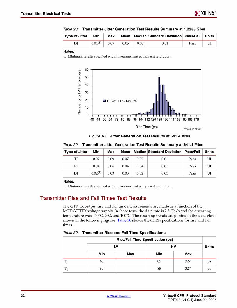
The test results are shown in Figure 14 through Figure 16 and summarized in Table 27 through Table 29.
Figure 14: Jitter Generation Test Results at 2.4576 Gb/s
Table 27: Transmitter Jitter Generation Test Results Summary at 2.4576 Gb/s
Type of Jitter Min Max Mean Median Standard Deviation Pass/Fail Units
TJ 0.15 0.29 0.22 0.21 0.02 Pass UI
RJ 0.08 0.26 0.15 0.15 0.02 Pass UI
DJ 0(1) 0.15 0.07 0.07 0.02 Pass UI
Notes: 1. Minimum results specified within measurement equipment resolution.
Figure 15: Jitter Generation Test Results at 1.2288 Gb/s
Table 28: Transmitter Jitter Generation Test Results Summary at 1.2288 Gb/s
Type of Jitter Min Max Mean Median Standard Deviation Pass/Fail Units
TJ 0.12 0.17 0.12 0.12 0.01 Pass UI
RJ 0.08 0.18 0.07 0.07 0.01 Pass UI
180
160
140
80
20
40
100
120
60
0
0.00
00.
0250.
050
0.10
00.
075
0.12
50.
0500.
175
TJ(UI)
0.20
0
Dat
a P
oint
s
0.22
50.
2750.
3000.
3250.
3500.
3750.
400
0.45
00.
4750.
500
0.42
5
RPT066_14_011607
60
50
40
20
30
10
0
RT AVTTTX=1.2V+5%
Rise Time (ps)
Num
ber
of G
TP
Tra
nsce
iver
s
RPT066_15_011607
40 48 56 64 72 80 88 96 104 112 120 128 136 144 152 160 165 176
32 www.xilinx.com Virtex-5 CPRI Protocol StandardRPT066 (v1.0.1) June 22, 2007
Transmitter Electrical TestsR
Transmitter Rise and Fall Times Test ResultsThe GTP TX output rise and fall time measurements are made as a function of the MGTAVTTTX voltage supply. In these tests, the data rate is 2.5 Gb/s and the operating temperature was –40°C, 0°C, and 100°C. The resulting trends are plotted in the data plots shown in the following figures. Table 30 shows the CPRI specifications for rise and fall times.
DJ 0.04(1) 0.09 0.05 0.05 0.01 Pass UI
Notes: 1. Minimum results specified within measurement equipment resolution.
Figure 16: Jitter Generation Test Results at 641.4 Mb/s
Table 29: Transmitter Jitter Generation Test Results Summary at 641.4 Mb/s
Type of Jitter Min Max Mean Median Standard Deviation Pass/Fail Units
TJ 0.07 0.09 0.07 0.07 0.01 Pass UI
RJ 0.04 0.06 0.04 0.04 0.01 Pass UI
DJ 0.02(1) 0.03 0.03 0.02 0.01 Pass UI
Notes: 1. Minimum results specified within measurement equipment resolution.
Table 28: Transmitter Jitter Generation Test Results Summary at 1.2288 Gb/s
Type of Jitter Min Max Mean Median Standard Deviation Pass/Fail Units
60
50
40
20
30
10
040 48 56 64 72 80 88 96 104 112 120 128 136 144 152 160 165 176
RT AVTTTX=1.2V-5%
Rise Time (ps)
Num
ber
of G
TP
Tra
nsce
iver
s
RPT066_16_011607
Table 30: Transmitter Rise and Fall Time Specifications
Rise/Fall Time Specification (ps)
UnitsLV HV
Min Max Min Max
Tr 60 85 327 ps
Tf 60 85 327 ps

Virtex-5 CPRI Protocol Standard www.xilinx.com 33RPT066 (v1.0.1) June 22, 2007
Transmitter Electrical TestsR
Figure 17 and Figure 18 shows the histogram distribution of the rise time of the XCV5LX50T TX side output at a 2.5 Gb/s data rate, with a 00001111 data pattern, and MGTAVTTTX equal to 1.2V ± 5%. Table 31 summarizes the transmitter rise time.
Figure 19 and Figure 20 show the histogram distribution of the fall time of the XCV5LX50T TX side output at a 2.5 Gb/s data rate, with a 00001111 data pattern, and MGTAVTTTX equal to 1.2V ± 5%. Table 32 summarizes the transmitter fall time.
Figure 17: XC5VLX50T Rise Time MGTAVTTTX = 1.26V
Figure 18: XC5VLX50T Rise Time MGTAVTTTX = 1.14V
Table 31: Transmitter Rise Time Summary
Min Max Mean Median Standard Deviation Pass/Fail Units
92 162 126 127 9.43 Pass ps
200
50
100
250
300
150
0
0.00
00.
0250.
050
0.10
00.
075
0.12
50.
0500.
175
TJ(UI)
0.20
0
Dat
a P
oint
s
0.22
50.
2750.
3000.
3250.
3500.
3750.
400
0.45
00.
4750.
500
0.42
5
RPT066_17_011607
200
50
100
350
250
300
400
150
0
0.00
00.
0250.
050
0.10
00.
075
0.12
50.
0500.
175
TJ(UI)
0.20
0
Dat
a P
oint
s
0.22
50.
2750.
3000.
3250.
3500.
3750.
400
0.45
00.
4750.
500
0.42
5
RPT066_18_011607

34 www.xilinx.com Virtex-5 CPRI Protocol StandardRPT066 (v1.0.1) June 22, 2007
Transmitter Electrical TestsR
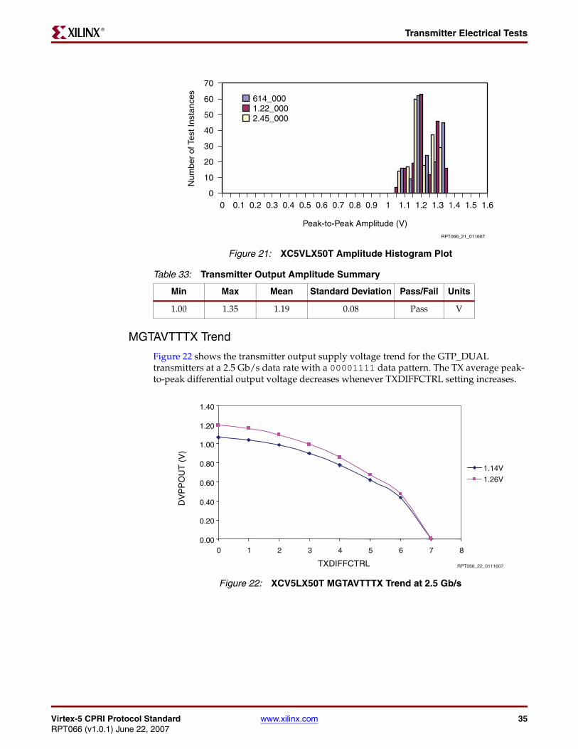
Transmitter Differential Amplitude Test Results
The transmitter differential amplitudes measures the differential voltage amplitude between the positive and negative GTP transceiver pins when the transmit eye is fully open. See Table 23, page 26 for amplitude limits.
The histogram plots (Figure 21) show the transmitter peak-to-peak output amplitude for all three CPRI specific data rates, and for TXDIFFCTRL= 000.
Figure 19: XC5VLX50T Fall Time at MGTAVTTTX = 1.26V
Figure 20: XC5VLX50T Fall Time at MGTAVTTTX = 1.14V
Table 32: Transmitter Fall Time Summary
Min Max Mean Median Standard Deviation Pass/Fail Units
70 148 105 105 12.29 Pass ps
30
25
20
10
15
5
0
FT AVTTTX=1.2V+5%
Fall Time (ps)
Num
ber
of G
TP
Tra
nsce
iver
s
RPT066_19_011607
40 48 56 64 72 80 88 96 104 112 120 128 136 144 152 160 165 176
30
25
20
10
15
5
0
FT AVTTTX=1.2V-5%
Fall Time (ps)
Num
ber
of G
TP
Tra
nsce
iver
s
RPT066_20_011607
40 48 56 64 72 80 88 96 104 112 120 128 136 144 152 160 165 176
Virtex-5 CPRI Protocol Standard www.xilinx.com 35RPT066 (v1.0.1) June 22, 2007
Transmitter Electrical TestsR
MGTAVTTTX Trend
Figure 22 shows the transmitter output supply voltage trend for the GTP_DUAL transmitters at a 2.5 Gb/s data rate with a 00001111 data pattern. The TX average peak-to-peak differential output voltage decreases whenever TXDIFFCTRL setting increases.
Figure 21: XC5VLX50T Amplitude Histogram Plot
Table 33: Transmitter Output Amplitude Summary
Min Max Mean Standard Deviation Pass/Fail Units
1.00 1.35 1.19 0.08 Pass V
70
60
50
40
30
20
10
00 0.1 0.2 0.3 0.4 0.5
Peak-to-Peak Amplitude (V)
614_000
Num
ber
of T
est I
nsta
nces
0.6 0.7 0.8 0.9 1 1.1 1.2 1.3 1.4 1.5 1.6
1.22_0002.45_000
RPT066_21_011607
Figure 22: XCV5LX50T MGTAVTTTX Trend at 2.5 Gb/s
0.00
0.20
0.40
0.60
0.80
1.00
1.20
1.40
0 1 2 3 4 5 6 7 8
TXDIFFCTRL
DV
PP
OU
T (
V)
1.14V
1.26V
RPT066_22_0111607

36 www.xilinx.com Virtex-5 CPRI Protocol StandardRPT066 (v1.0.1) June 22, 2007
Transmitter Electrical TestsR
Temperature Trend
Figure 23 shows the temperature trend at a 2.5 Gb/s data rate with a 00001111 data pattern. The temperature does not have significant effects on the TX average peak-to-peak differential output voltage. Minimal amplitude differences were seen due to changes in data rate.
Figure 23: XCV5LX50T Temperature Trend at 2.5 Gb/s
1.4
1.2
1
0.8
0.6
0.4
0.2
0
0 1 2 3 4 5 6 7
TXDIFFCTRL
DV
PP
OU
T(V
)
8
RPT066_23_011607
–40oC
0oC
100oC
Virtex-5 CPRI Protocol Standard www.xilinx.com 37RPT066 (v1.0.1) June 22, 2007
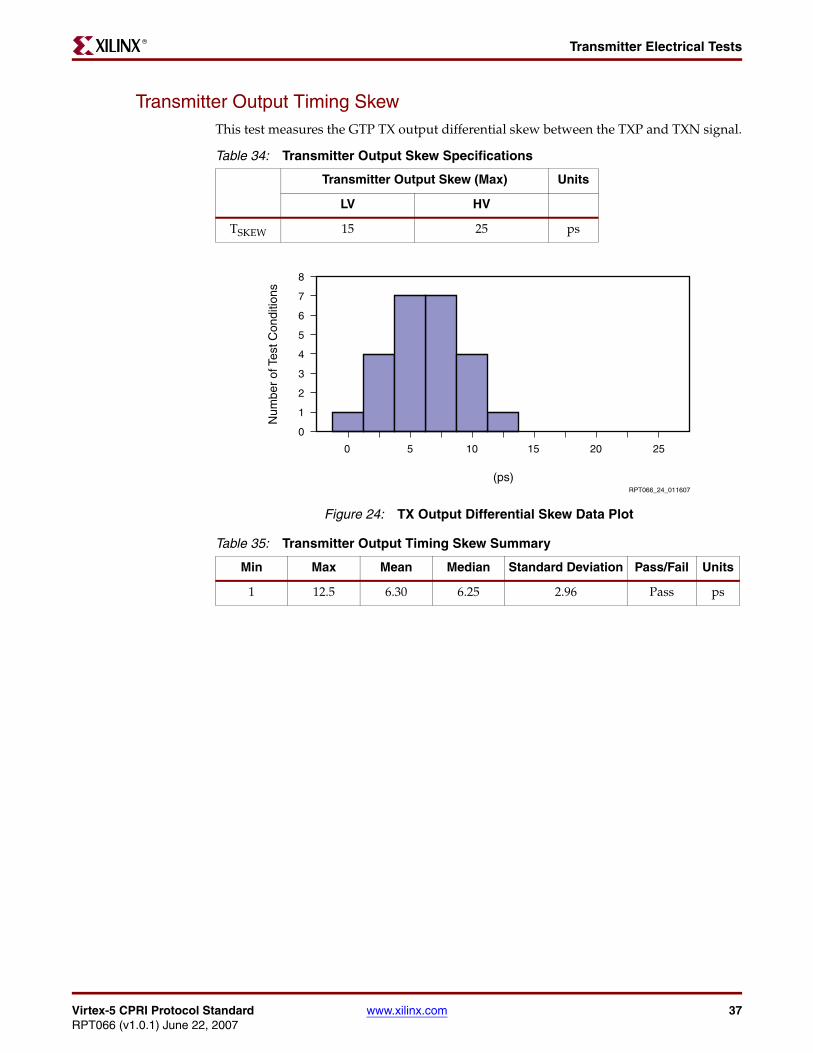
Transmitter Electrical TestsR
Transmitter Output Timing SkewThis test measures the GTP TX output differential skew between the TXP and TXN signal.
Table 34: Transmitter Output Skew Specifications
Transmitter Output Skew (Max) Units
LV HV
TSKEW 15 25 ps
Figure 24: TX Output Differential Skew Data Plot
Table 35: Transmitter Output Timing Skew Summary
Min Max Mean Median Standard Deviation Pass/Fail Units
1 12.5 6.30 6.25 2.96 Pass ps
7
4
3
2
1
5
8
6
0
0 5 10 2015 25
(ps)
Num
ber
of T
est C
ondi
tions
RPT066_24_011607
38 www.xilinx.com Virtex-5 CPRI Protocol StandardRPT066 (v1.0.1) June 22, 2007
Transmitter Electrical TestsR
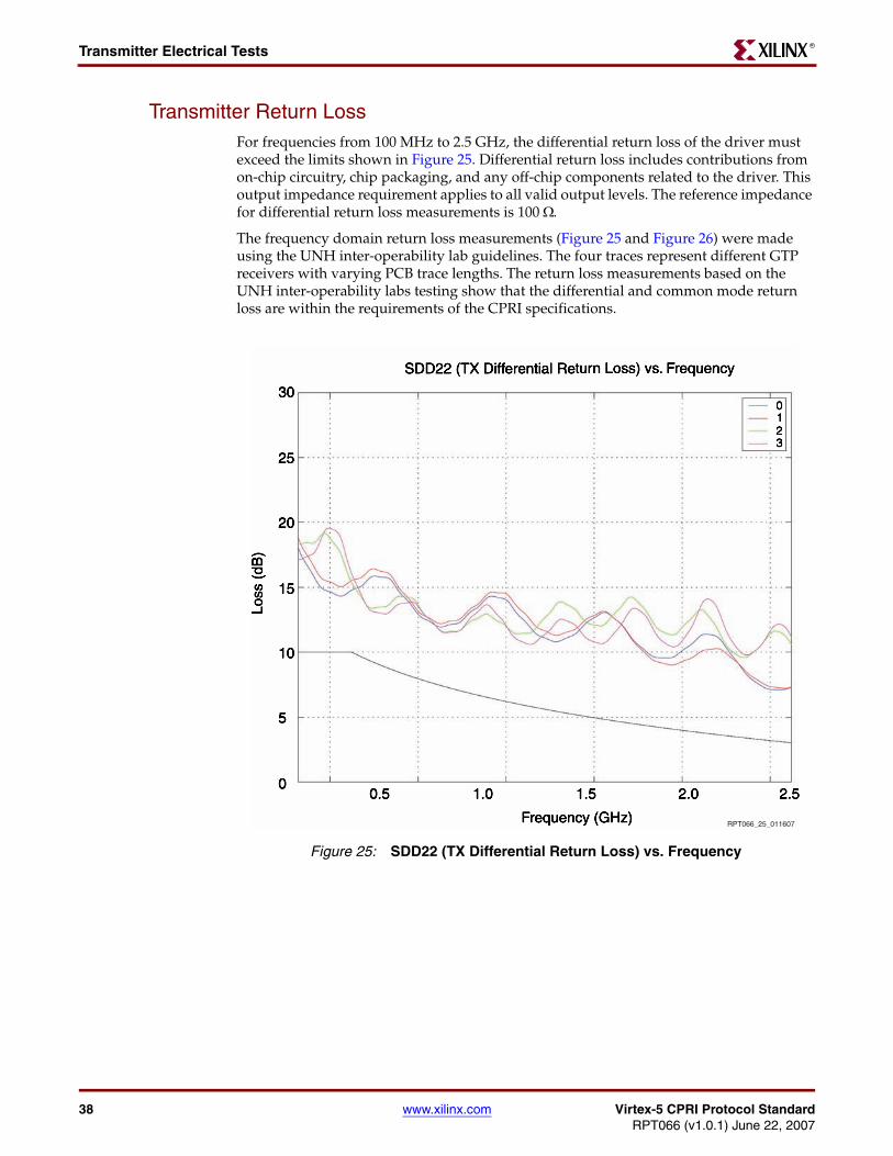
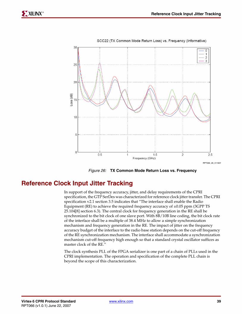
Transmitter Return LossFor frequencies from 100 MHz to 2.5 GHz, the differential return loss of the driver must exceed the limits shown in Figure 25. Differential return loss includes contributions from on-chip circuitry, chip packaging, and any off-chip components related to the driver. This output impedance requirement applies to all valid output levels. The reference impedance for differential return loss measurements is 100 Ω.
The frequency domain return loss measurements (Figure 25 and Figure 26) were made using the UNH inter-operability lab guidelines. The four traces represent different GTP receivers with varying PCB trace lengths. The return loss measurements based on the UNH inter-operability labs testing show that the differential and common mode return loss are within the requirements of the CPRI specifications.
Figure 25: SDD22 (TX Differential Return Loss) vs. Frequency
RPT066_25_011607
Virtex-5 CPRI Protocol Standard www.xilinx.com 39RPT066 (v1.0.1) June 22, 2007
Reference Clock Input Jitter TrackingR
Reference Clock Input Jitter TrackingIn support of the frequency accuracy, jitter, and delay requirements of the CPRI specification, the GTP SerDes was characterized for reference clock jitter transfer. The CPRI specification v2.1 section 3.5 indicates that “The interface shall enable the Radio Equipment (RE) to achieve the required frequency accuracy of ±0.05 ppm (3GPP TS 25.104[8] section 6.3). The central clock for frequency generation in the RE shall be synchronized to the bit clock of one slave port. With 8B/10B line coding, the bit clock rate of the interface shall be a multiple of 38.4 MHz to allow a simple synchronization mechanism and frequency generation in the RE. The impact of jitter on the frequency accuracy budget of the interface to the radio base station depends on the cut-off frequency of the RE synchronization mechanism. The interface shall accommodate a synchronization mechanism cut-off frequency high enough so that a standard crystal oscillator suffices as master clock of the RE.”
The clock synthesis PLL of the FPGA serializer is one part of a chain of PLLs used in the CPRI implementation. The operation and specification of the complete PLL chain is beyond the scope of this characterization.
Figure 26: TX Common Mode Return Loss vs. Frequency
RPT066_26_011607

40 www.xilinx.com Virtex-5 CPRI Protocol StandardRPT066 (v1.0.1) June 22, 2007
Reference Clock Input Jitter TrackingR
Test Setup
Reference clock input jitter tolerance measurements are performed using the test setup in Figure 27.
• At 2.4576 Gb/s, each vertical scale jitter tolerance number in UI should be divided by 20 to get the jitter tolerance UI value in terms of reference clock UI (1 UI = 8.138 ns for 122.88 MHz reference clock frequency.) For example, if the injected jitter which caused the failure was 0.2 UI at 2.4576 Gb/s (period = 406.9 ps), this would translate to 406.9 ps x 0.2 UI = 81.38 ps.
• At 1228.8 Mb/s, each vertical scale jitter tolerance number in UI should be divided by 10 to get the jitter tolerance UI value in terms of reference clock UI (1 UI = 8.138 ns for 122.88 MHz reference clock frequency). For example, 20 UI of plotted jitter tolerance amplitude is 2 UI (20/10) at the reference clock frequency of 122.88 MHz.
• At 614.4 MB/s, each vertical scale jitter tolerance number in UI should be divided by 5 to get the jitter tolerance UI value in terms of reference clock UI (1 UI = 8.138 ns for 122.88 MHz reference clock frequency). For example, 20 UI of plotted jitter tolerance amplitude is 4 UI (20/5) at the reference clock frequency of 122.88 MHz.
Figure 27: Reference Clock Input Jitter Tolerance Test Setup
Blue denotes back panel connection.
GPIB
HP-MSIB
HP-MSIB
Clk In
Trigger Out
Error Detector
Error Out
Error InCLK
SUB CLK
DATA
Clock Out N/P
Clock In Data In
TXN
RXN20
20
RXP
REF CLK
RPT066_27_011607
Channel 1
External TriggerChannel 2
TXP
Data Out N/P
= 2.4576 Gbps= 1228.9 MHz (RxDivSel_Out=1)= 122.88 MHz
= 1228.8 Mbps= 1228.8 MHz (RxDivSel_Out=2)= 122.88 MHz
= 614.4 Mbps= 1228.8 MHz (RxDivSel_Out=4)= 122.88 MHz
Target Line RateVCO Frequency
RefClk Frequency
Target Line RateVCO Frequency
RefClk Frequency
Target Line RateVCO Frequency
RefClk Frequency
83752A Clock Source
86100A Infinium DCA Scope
70004A Display
70832B 12 Gbps BERTPattern Generator
ML523Board
Xaui Backplane 30 Inch
BIAS-T
N4903A JBERT
70340A Sig Gen1-20 GHz

Virtex-5 CPRI Protocol Standard www.xilinx.com 41RPT066 (v1.0.1) June 22, 2007
Reference Clock Input Jitter TrackingR
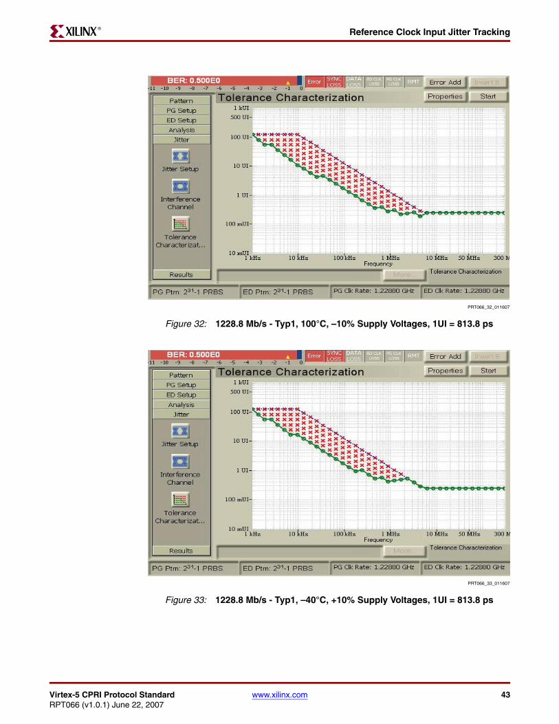
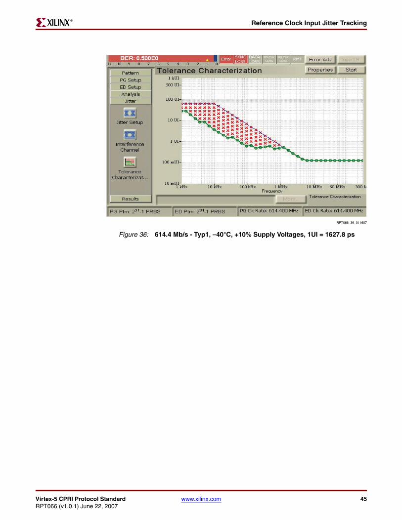
In the following figures, the green dots represent the passing data points, the red cross-stitch marks represent the failing points, and the blue line on top represents the equipment test limit.
Figure 28: 2.4576 Gb/s - Typ1, 25°C, Nominal Supply Voltages, 1UI = 406.9 ps
Figure 29: 2.4576 Gb/s - Typ1, 100°C, –10% Supply Voltages, 1UI = 406.9 ps
RPT066_28_011607
RPT066_29_011607
42 www.xilinx.com Virtex-5 CPRI Protocol StandardRPT066 (v1.0.1) June 22, 2007
Reference Clock Input Jitter TrackingR
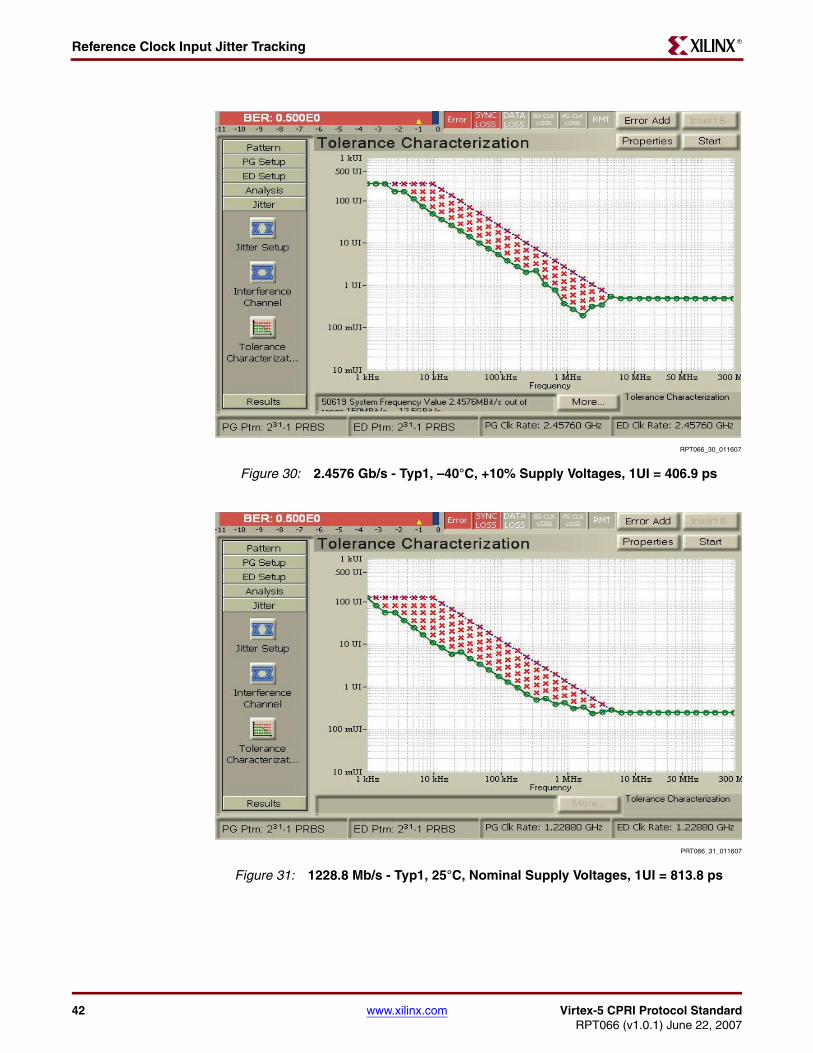
Figure 30: 2.4576 Gb/s - Typ1, –40°C, +10% Supply Voltages, 1UI = 406.9 ps
Figure 31: 1228.8 Mb/s - Typ1, 25°C, Nominal Supply Voltages, 1UI = 813.8 ps
RPT066_30_011607
PRT066_31_011607
Virtex-5 CPRI Protocol Standard www.xilinx.com 43RPT066 (v1.0.1) June 22, 2007
Reference Clock Input Jitter TrackingR
Figure 32: 1228.8 Mb/s - Typ1, 100°C, –10% Supply Voltages, 1UI = 813.8 ps
Figure 33: 1228.8 Mb/s - Typ1, –40°C, +10% Supply Voltages, 1UI = 813.8 ps
PRT066_32_011607
PRT066_33_011607

44 www.xilinx.com Virtex-5 CPRI Protocol StandardRPT066 (v1.0.1) June 22, 2007
Reference Clock Input Jitter TrackingR
Figure 34: 614.4 Mb/s - Typ1, 25°C, Nominal Supply Voltages, 1UI = 1627.8 ps
Figure 35: 614.4 Mb/s - Typ1, 100°C, –10% Supply Voltages, 1UI = 1627.8 ps
RPT066_34_011607
RPT066_35_011607
Virtex-5 CPRI Protocol Standard www.xilinx.com 45RPT066 (v1.0.1) June 22, 2007
Reference Clock Input Jitter TrackingR
Figure 36: 614.4 Mb/s - Typ1, –40°C, +10% Supply Voltages, 1UI = 1627.8 ps
RPT066_36_011607