Embed Size (px)
Citation preview

VIII-Ⅱ-1. Project Research
Project 1

PR1 Irradiation Effects on Microstructural Evolution in Materials Irradiated by Particles with High Energy
Q. Xu
Research Reactor Institute, Kyoto University
OBJECTIVES: Neutron irradiations in KUR have been used to not only estimate degradation mechanical proper-ties of materials but also develop new materials, such as material for optoelectronic and high-power devices. In addition, other irradiation facilities, such as ions, elec-trons and γ rays, have also been used in the present pro-ject research to clarify the damage structural develop-ment.
RESULTS: The allotted research subject (ARS) and the name of co-researches in each ARS are listed below. Ferritic steels containing Cr are expected to be used for the first-wall component in fusion reactors. Neutron irra-diation induced phase separation in Fe-30Cr binary alloy. Transmutation of 14C, which related luminescence and net carrier concentration, in GaN by a (n, p) reaction of 14N was reported. Others results are presented in detail in this progress reports. ARS-1 Neutron-transmuted Carbon-14 in neutron-irradiated GaN compensation of DX-like center (K. Kuriyama, T. Ida, K. Kamioka, K. Kushida, and Q. Xu) ARS-2 Neutron irradiation effects of superconducting magnet materials at low temperature (T. Nakamoto, M. Yoshida, T. Ogitsu, Y. Makida, K. Yo-shimura, S. Mihara, K. Sasaki, M. Sugano, H. Nishiguchi, M. Iio, Y. Kuno, M. Aoki, A. Sato, T. Itahashi, Q. Xu, K. Sato, Y. Kuriyama, Y. Mori and T. Yoshiie) ARS-3 Study on formation and recovery processes of radiation damage in crystalline materials (A. Kinomura, K. Sato, Q. Xu and T. Yoshiie) ARS-4 Blue emission of natural calcite by gamma rays (T. Awata, Y. Bando and Q. Xu) ARS-5 Annealing behavior of thermal diffusivity in ceramics irradiated by 30 MeV electron and neutron
(M. Akiyoshi, I. Takagi, T. Yoshiie, Q. Xu, K. Sato)
ARS-6 Annealing behavior of vacancy-type defects in Mg-Zn-Y alloy with LPSO structure introduced by electron-irradiation at liqiud nitrogen temperature (Y. Nagai, K. Inoue, T. Toyama, Y. Matsukawa, Y. Shimizu, A. Kuramoto, H. Takamizawa, Y. Kakubo, T. Yoshiie, Q. Xu and K. Sato) ARS-7 Radiation damage in bulk amorphous alloys by electron irradiation (F.Hori, N. Onodera, A.Ishii, S.Mineno, A.Iwase, Y. Yokoyama, Q.Xu, K.Sato and T.Yoshiie) ARS-8 Development of replica extraction method for vanadium alloys and its application for neutron-irradiated ones (K. Fukumoto and Q. Xu) ARS-9 Damage evolution in neutron-irradiated metals during neutron irradiation at elevated temperatures (I.Mukouda, K. Yamakawa, T. Yoshiie, Q. Xu) ARS-10 Positron annihilation behavior of Fe-Cr alloys after neu-tron irradiation in KUR (R. Kasada, K. Sato, Q. Xu, T. Yoshiie) ARS-11 Similarity of radiation resistance of nanocrystalline Ni by ion and neutron irradiation (H. Tsuchida, A. Itoh, K. Sato, T. Yoshiie, Q. Xu) ARS-12 Interaction between deuterium and defects in tungsten (2) (K. Sato, R. Tamiya, Q. Xu and T. Yoshiie) ARS-13 Irradiation effects on stress loading property of refractory metal at high temperature (K. Tokunaga, K. Araki, T. Ukita, Q. Xu, T. Yoshiie) ARS-14 Effect of substrate temperature in nanocell fabrication of GaSb (N. Nitta, K. Yokoyama and M. Taniwaki ARS-15 Deuterium retention in electron-irradiated VPS-W Y. Hatano. J. Shi, T. Nozaki, K. Masude, T. Tokunaga, H. Watanabe, N. Yoshida, K. Sato and Q. Xu
採択課題番号 24P1 材料の組織変化に及ぼす高エネルギー粒子線の照射効果 プロジェクト
(京大・原子炉)徐 虬

PR1-1 Neutron-Transmuted Carbon-14 in Neutron-Irradiated GaN: Compensation of DX-like Center
K. Kuriyama, T. Ida, K. Kamioka, K. Kushida1 and Q. Xu2 College of Engineering and Research Center of Ion Beam Technology, Hosei University 1Osaka Kyoiku University 2Research Reactor Institute, Kyoto University INTRODUCTION: In our previous study [1], we re-ported that Ge atoms were transmuted into Ga in GaN by a (n,γ) reaction of 69Ga and 71Ga, which acted as do-nors. 14C atoms would be also transmuted from 14N in GaN by a (n,p) reaction of 14N. In the present study, we report the transmutation of 14C in GaN by a (n,p) reaction of 14N. The transmuted 14C related luminescence and net carrier concentration are studied by combining photolu-minescence, liquid scintillation, and Raman scattering. EXPERIMENTS: GaN single crystal films grown by metalorganic-vapor-phase epitaxy were irradiated with fast and thermal neutrons at fluxes of 3.9 x 1013 cm-2s-1 and 8.15 x 1013 cm-2s-1, respectively. Irradiation time was 48 hours. The calculated 72Ge and 14C concentrations were 1.24 x 1018 cm-3 and 1.13 x 1018 cm-3, respectively. RESULTS: The transmuted 14C was studied by the liq-uid scintillation method to detect β-rays emitted in the process of 14C decays from 14N. Tritium (3H) is also emitted by a (n,t) reaction of 14N due to the neutron irra-diation above 4.5 MeV. Figure 1 shows the liquid scintil-lation spectra of NTD-GaN. The transmuted 3H concen-tration is three orders of magnitude lower than that of 14C. However, the radiation dose of the emitted 3H is ten times higher than that of 14C. This attributes to the dif-ference of the half-life, namely 14C has a half-life of 5730 years, but that of 3H is 12.33 years. The short half-life elements release more radiation.
As shown in figure 2, photoluminescence relating to carbon [2], DX-like center of Ge [1], and yellow lumi-nescence band (YL) relating to the crystal defects by fast neutron was observed in 1000 oC annealed NTD-GaN.
Figure 3 shows a Raman spectrum. The peaks at 421 cm-1 and 756 cm-1 are related to the sapphire substrate. The spectra relating to the NTD-GaN are observed at 740 cm-1 and 575 cm-1. The free electron concentration (N) estimated from N = 1.1 x 10¹⁷ (νmax - 736) 0.764 [3], where νmax is the LO mode frequency, is 3.17 x 1017 cm-3. This value is lower than that from the transmuted Ge concen-tration. Therefore, the DX-like center of Ge [1] would be
compensated by the transmuted 14C acceptor. Fig 1. Liquid scintillation spectra of NTD-GaN. Fig 2. Photoluminescence spectra of 1000 oC annealed NTD-GaN. Fig 3. Raman spectra of 1000 oC annealed NTD-GaN. REFERENCES: [1] K. Kuriyama, T. Tokumasu, J. Takahashi, H. Kondo,
and M. Okada, Appl. Phys. Lett. 80, (2002) 3328; [2] S. Fischer, C. Wetzel, and E. E. Haller, and B. K.
Meyer, Appl. Phys. Lett. 67, (1995) 1298. [3] C. Wetzel, W. Walukiewicz, E. E. Haller, J. Ager Ⅲ, I.
Grzegory, S. Porowski, and T. Suski, Phys. Rev. B 53, (1996) 1322.
A part of this work was presented in 31th Int. Conf. Physics of Semiconductors in Zurich (2012, July. 30 ~ August. 2).
採択課題番号 24P1-1 化合物半導体の照射効果と電気的・光学的物性に関する研究 プロジェクト
(法政大院)栗山一男、伊田孝寛、上岡一馬(大阪教育大)串田一雅
(京大・原子炉)徐 虬

プロジェクト
Neutron Irradiation Effects of Superconducting Magnet Materials at Low Temperature
T. Nakamoto, M. Yoshida, T. Ogitsu, Y. Makida, K. Yoshimura, S. Mihara, K. Sasaki, M. Sugano, H. Nishiguchi, M. Iio, Y. Kuno1, M. Aoki1, A. Sato1, T. Itahashi1, Q. Xu2, K. Sato2, Y. Kuriyama2, Y. Mori2 and T. Yoshiie2
J-PARC Center, KEK 1Department of Physics, Osaka University 2Research Reactor Institute, Kyoto University
INTRODUCTION: The superconducting magnets will be subjected to a high neutron fluence of 1021 n/m2 or higher in the operation life time in the high energy particle physics experiments, such as a high luminosity upgrade of the LHC at CERN and the muon source for the COMET experiment at J - P A R C. Since electrical resistivity of a stabilizer at low temperature, which is very sensitive to neutron irradiation, is one of the important parameters for the quench protection of the magnet system. A series of electrical resistivity measurement at neutron irradiation for the aluminum stabilizer with additives of yttrium taken from the prototype superconducting cable as well as copper stabilizer was started in 2011. In 2012, the second irradiation test with the same samples in 2011 was performed to observe the effect of the multiple irradiations and the thermal cycles to room temperature. EXPERIMENTS: The irradiation tests have been carried out at a low temperature irradiation facility (LTL) at E-4 line of KUR. The aluminum stabilizer samples (RRR~350) with dimensions of 1 mm x 1 mm x 70 mm were cut from the superconducting cable manufactured by Hitachi Cable. The copper stabilizer sample (RRR~300) also has the same dimensions. The electric resistance was measured by a 4-wire method employing a Keithley 6221 current source and a Keithley 2182A voltmeter. The temperature was determined by using a thermocouple of Au(Fe) and Chromel, since the Cernox sensor (CX-1050-SD) showed a temperature drift during neutron exposure due to the irradiation damage. The thermocouple and the Cernox sensor and placed just behind the samples to measure the temperature of the helium gas coolant. RESULTS: The second irradiation test for two aluminum samples (Al-Y1, Al-Y2) and one copper sample was carried out in Nov. 2012. The irradiation condition is basically same as the first irradiation in 2011. After cooling down to 13 K, the reactor was turned on to a power of 1 MW. The estimated fast neutron fluence in 52 hour operation is 2.6 x 10²⁰ n/m2. Resistance of the samples and temperature variations during the irradiation are shown in Fig. 1. The temperature jumped from 13 K to 15 K at the beginning due to radiation from the reactor
core. During exposure the thermocouple indicates stable temperature while the Cernox sensor readout drifts up to 18 K due to irradiation damage. Behavior of the induced resistance by the neutron irradiation is very similar to the previous results in 2011: the resistance shows linear increase with respect to the neutron fluence during the exposure. Degradation rates of the electrical resistivity at the fluence of 1020 n/m2 are 2.7 x 101 pΩm and 1.0 x 101 pΩm for the aluminum and the copper samples, respectively. Anneal effects of the samples due to the thermal cycle to room temperature were observed. For the aluminum samples, the induced resistance was fully recovered to be the original resistance by the thermal cycles for the first and the second neutron irradiations. For the copper sample, however, the recovery of the resistance by the thermal cycle was imperfect. The recovery rates, defined as how much induced electrical resistivity due to the irradiation is recovered by the thermal cycle, were 84 % and 96 % for the first and the second irradiations, respectively. These results seem to be consistent with the previous works. SUMMARY: A series of neutron irradiation tests have been pursued at KUR, with the aim of R&D for radiation hard superconducting magnets. The aluminum stabilizer with yttrium additive and the copper stabilizer from the superconducting cable were irradiated in 2011 and 2012 in order to investigate the multiple irradiation effects and the anneal effects by the thermal cycles on electrical resistivity. Each sample showed consistent resistivity increase in the first and the second irradiation runs. A full recovery of the resistivity was confirmed in the aluminum sample while the copper sample indicated the recovery rate of around 90 %.
Fig.1. Electrical resistance of aluminum and copper
stabilizer samples during the neutron irradiation in 2012.
PR1-2

採択課題番号 24P1-3 結晶材料における照射損傷形成と回復過程の研究 プロジェクト
(産総研)木野村淳(京大・原子炉)佐藤紘一、徐 、義家敏正
Study on Formation and Recovery Processes of Radiation Damage in Crystalline Materials
A. Kinomura, K. Sato1, Q. Xu1 and T. Yoshiie1
National Institute of Advanced Industrial Science and Technology (AIST) 1 Kyoto University Research Reactor Institute (KURRI)
INTRODUCTION: Radiation effects of ion irradiation have been extensively studied for various materials. In general, radiation damage degrades crystallinity and gives harmful effects on material properties. However, under appropriate irradiation or annealing conditions, the radiation effects can induce interesting phenomena or useful structures in materials. A typical example of such effects is the ion beam annealing in Si, where implantation-induced damage layers are recrystallized by other ion irradiation. Thus, it is important to investigate the radiation effects of energetic particles (ions and neutrons) with materials. EXPERIMENTS: Two types of experiments have been performed so far. As the first experiment, neutron enhanced annealing of ion-implantation induced damage in single-crystalline Si was studied. Si ion implantation to crystalline Si samples was performed at 200 keV to doses of 5×10¹⁴ – 2×1015 cm-2 to induce radiation damage or amorphous phases. The damaged Si samples were neutron-irradiated in the KUR (Kyoto University Reactor) core or SSS irradiation facilities. The samples with and without neutron irradiation were characterized by Rutherford backscattering/channeling (RBS/C). As the second exeriment, gettering of metal impurities to hydrogen-implanted multicrystalline Si was studied. The multicrystalline Si was implanted with 50 keV H+ to a dose of 3×1016 cm-2 and annealed at 750 or 850 ºC for 1h. The gettering effect of metal impurities was characterized by neutron activation analysis using the core or hydronuematic irradiation facilities of KUR. RESULTS: In the neutron enhanced annealing experiments, annealing effects were negligible in the case of amorphized samples (with doses of 1 or 2×1015 cm-2). The heavily damaged samples (with a dose of 5×1014 cm-2) showed sufficient annealing effects for the core and SSS irradiations. The sample temperature of the SSS irradiation was accurately controlled at 400 ºC. On the other hand, the sample temperature of the core irradiation cannot be measured during the neutron irradiation, although the water temperature in the KUR core can be measured. Thus it is important to estimate the sample
temperature of the irradiation capsule. We numerically solved one- or two-dimensional partial differential equation of heat flow for the Si sample in a KUR core irradiation capsule. The capsule consists of outer and inner sub-capsules made of Al. He gas was introduced in the capsule. The ambient temperature of the capsule was adjusted to the water temperature of the reactor core (49 ºC in this calculation). Such information together with capsule and sample sizes was put in the calculation. Figure 1 shows the calculated temperature distributions (cross-sectional views) of the core irradiation capsule with Si samples. Fig. 1(a) and 1(b) assumed the circular and the rectangular sample shape with the same cross-sectional area. The maximum temperatures in the capsule were 85 and 81 ºC for Fig. 1(a) and 1(b), respectively. From these calculations, the sample temperature during the neutron irradiation at the KUR core irradiation facility was estimated to be less than 90 ºC. The RBS/C spectra of the control sample thermally annealed at 90 ºC showed that the damage peak was bigger than that of the neutron irradiated sample. We confirmed that the neutron enhanced annealing occurred in the core irradiation as well as in the SSS irradiation at 400 ºC. The specimen for cross-section TEM (transmission electron microscophy) for the gettering experiment was prepared by the FIB milling machine. The best milling condition was determined and the further sample preparation is in progress. In summary, the sample temperature during neutron irradiation of the core irradiation facility was calculated. The FIB-milling condition for the multicrysalline Si sample for the gettering experiment was determined. ACKNOWLEDGMENT: We would like to thank colleagues in AIST for their assistance on this study.
Fig. 1 Calculated temperature distributions (cross sectional views) inside the KUR core irradiation capsule with Si samples. The circular (a) and rectangular (b) shapes of the samples were assumed.
(a) (b)
PR1-3
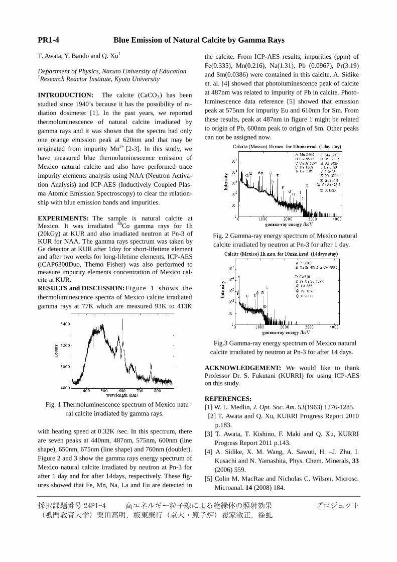
PR1-4 Blue Emission of Natural Calcite by Gamma Rays T. Awata, Y. Bando and Q. Xu1 Department of Physics, Naruto University of Education 1Research Reactor Institute, Kyoto University INTRODUCTION: The calcite (CaCO3) has been studied since 1940’s because it has the possibility of ra-diation dosimeter [1]. In the past years, we reported thermoluminescence of natural calcite irradiated by gamma rays and it was shown that the spectra had only one orange emission peak at 620nm and that may be originated from impurity Mn2+ [2-3]. In this study, we have measured blue thermoluminescence emission of Mexico natural calcite and also have performed trace impurity elements analysis using NAA (Neutron Activa-tion Analysis) and ICP-AES (Inductively Coupled Plas-ma Atomic Emission Spectroscopy) to clear the relation-ship with blue emission bands and impurities. EXPERIMENTS: The sample is natural calcite at Mexico. It was irradiated 60Co gamma rays for 1h (20kGy) at KUR and also irradiated neutron at Pn-3 of KUR for NAA. The gamma rays spectrum was taken by Ge detector at KUR after 1day for short-lifetime element and after two weeks for long-lifetime elements. ICP-AES (iCAP6300Duo, Themo Fisher) was also performed to measure impurity elements concentration of Mexico cal-cite at KUR. RESULTS and DISCUSSION: Figure 1 shows the thermoluminescence spectra of Mexico calcite irradiated gamma rays at 77K which are measured 93K to 413K
Fig. 1 Thermoluminescence spectrum of Mexico natu-
ral calcite irradiated by gamma rays. with heating speed at 0.32K /sec. In this spectrum, there are seven peaks at 440nm, 487nm, 575nm, 600nm (line shape), 650nm, 675nm (line shape) and 760nm (doublet). Figure 2 and 3 show the gamma rays energy spectrum of Mexico natural calcite irradiated by neutron at Pn-3 for after 1 day and for after 14days, respectively. These fig-ures showed that Fe, Mn, Na, La and Eu are detected in
the calcite. From ICP-AES results, impurities (ppm) of Fe(0.335), Mn(0.216), Na(1.31), Pb (0.0967), Pr(3.19) and Sm(0.0386) were contained in this calcite. A. Sidike et. al. [4] showed that photoluminescence peak of calcite at 487nm was related to impurity of Pb in calcite. Photo-luminescence data reference [5] showed that emission peak at 575nm for impurity Eu and 610nm for Sm. From these results, peak at 487nm in figure 1 might be related to origin of Pb, 600nm peak to origin of Sm. Other peaks can not be assigned now.
Fig. 2 Gamma-ray energy spectrum of Mexico natural calcite irradiated by neutron at Pn-3 for after 1 day.
Fig.3 Gamma-ray energy spectrum of Mexico natural
calcite irradiated by neutron at Pn-3 for after 14 days. ACKNOWLEDGEMENT: We would like to thank Professor Dr. S. Fukutani (KURRI) for using ICP-AES on this study. REFERENCES: [1] W. L. Medlin, J. Opt. Soc. Am. 53(1963) 1276-1285. [2] T. Awata and Q. Xu, KURRI Progress Report 2010
p.183. [3] T. Awata, T. Kishino, F. Maki and Q. Xu, KURRI
Progress Report 2011 p.143. [4] A. Sidike, X. M. Wang, A. Sawuti, H. –J. Zhu, I.
Kusachi and N. Yamashita, Phys. Chem. Minerals, 33 (2006) 559.
[5] Colin M. MacRae and Nicholas C. Wilson, Microsc. Microanal. 14 (2008) 184.
採択課題番号 24P1-4 高エネルギー粒子線による絶縁体の照射効果 プロジェクト
(鳴門教育大学)粟田高明,板東康行(京大・原子炉)義家敏正,徐虬

PR1-5 Annealing Behavior of Thermal Diffusivity in Ceramics Irradiated by 30MeV Electron and Neutron
M. Akiyoshi, I. Takagi, T. Yoshiie1, Q. Xu1 and K. Sato1 Faculty of Engineering, Kyoto University 1Research Reactor Institute, Kyoto University INTRODUCTION: It is well known that neutron-irradiated ceramics showed significant degradation in thermal diffusivity, while thermal diffusivity during the irradiation is still not estimated. A temperature of a specimen is calculated from the thermal conductivity easily, but at an irradiation con-dition, thermal conductivity of specimen decreased, and that rise the temperature of the specimen. The increased temperature anneals the irradiation induced defects, and that recover the thermal conductivity. To resolve this problem, kinetic analysis is required. In this analysis, most important information is the behavior of point de-fects. EXPERIMENTS: Accordingly, in this work, 30MeV electron accelerator KURRI-Linac is used to induce point-defects in bulk specimens of typical structural ceramics (AlN and β-SiC) to 1.5x1024e/m2 which correspond to 0.01dpa. The irradi-ation was performed in the water-cooled specimen holder at around 80℃. After the irradiation, isochronal annealing was con-ducted every 100℃ up to 1100℃ in vacuum using the SiC furnace of TC-7000H. Specimens were annealed for 1 h at an objective temperature. After the annealing, specimens were cooled in the furnace to the room tem-perature, and then thermal diffusivity was measured by the laser-flash method using a specially ordered meas-urement system (ULVAC Techno. TC-7000H/Special), and was analyzed with the t1/2 method. In addition, neutron-irradiations have been performed in the experimental fast reactor JOYO using CMIR-4 rig in previous works. The capsule T51 was irradiated to 28 dpa at 502℃ and the capsule T57 was irradiated to 37 dpa at 738℃. These samples were also isochronal annealed up to 1500℃ and measurements of thermal diffusivity were performed at room temperature. RESULTS: Figs. 1 and 2 show recovery behavior of the thermal diffusivity in the electron- and neutron-irradiated AlN and β-SiC ceramic specimens with isochronal annealing. The filled symbols in the figure represent the result from electron-irradiated specimen, and their thermal diffusivi-ties were shown with left-side axis. The error bar shows standard deviation among the values measured about 10 times. The open symbols represent the result from neu-tron-irradiated specimens. All electron-irradiated specimen showed the recovery of
thermal diffusivity from 400-500℃, and AlN specimens recovered linearly with the annealing temperature (Fig.1). The electron-irradiated β-SiC specimen (Fig.2) showed recovery from 400℃ with quadric curve. In the case of neutron-irradiated AlN, the onset temper-ature of recovery ( 800-900℃ ) is higher than and inde-pendent of the irradiation temperature. On the other hand, the electron-irradiated specimen recovered from 400-500℃, that is obviously lower than the onset tem-perature of recovery in neutron-irradiated specimens and higher than the irradiated temperature. The neu-tron-irradiated β-SiC showed almost same behavior as the electron-irradiated specimen at lower temperature. While the neutron-irradiated and β-SiC recovered rapidly with quadric curve above 1000℃. This difference may arise from the difference in the crystal structure discussed in a previous work, where the defect structure was explained by the pileup model (AlN) and nano-partition model (β-SiC).
0 500 1000 1500
0.40
0.50
0.60
0.70
0
0.10
0.20
Annealing Temperature / ℃
Ther
mal
Diff
usiv
ity /
10 -4
m2 /s
Electron irradiated AlN (KURL-0708, 0.01dpa at 80℃) Neutron irradiated AlN (T51, 28dpa at 502℃) Neutron irradiated AlN (T57, 37dpa at 738℃)
Fig.1 Recovery behavior of thermal diffusivity in elec-tron-irradiated AlN ceramic with isochronal annealing.
0 500 1000 15000
0.20
0.40
0.60
0.80
0.05
0.10
0.15
Annealing Temperature / ℃
Ther
mal
Diff
usiv
ity /
10 -4
m2 /s Electron irradiated β-SiC (KURL-0708, 0.01dpa at 80℃)
Neutron irradiated β-SiC (T51, 28dpa at 502℃) Neutron irradiated β-SiC (T57, 37dpa at 738℃)
Fig.2 Recovery behavior of thermal diffusivity in elec-tron-irradiated β-SiC ceramic with isochronal annealing.
採択課題番号 24P1-5 電子線照射後セラミックス中の欠陥評価 プロジェクト
(京大・工)秋吉 優史、高木 郁二(京大・原子炉)義家 敏正、徐 虫L、佐藤 紘一
PR1-6 Annealing Behavior of Vacancy-Type Defects in Mg-Zn-Y Alloy with LPSO Structure Introduced by Electron-irradiation at Liquid Nitrogen Temperature
Y. Nagai, K. Inoue, T. Toyama, Y. Matsukawa, Y. Shimi-zu, A. Kuramoto, H. Takamizawa, Y. Kakubo, T. Yoshiie1, Q. Xu1 and K. Sato1
Institute for Materials Research, Tohoku University 1Research Reactor Institute, Kyoto University
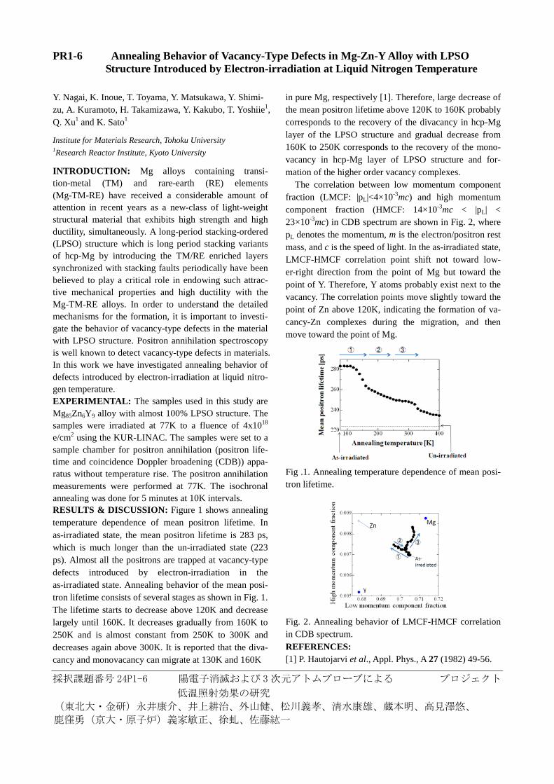
INTRODUCTION: Mg alloys containing transi-tion-metal (TM) and rare-earth (RE) elements (Mg-TM-RE) have received a considerable amount of attention in recent years as a new-class of light-weight structural material that exhibits high strength and high ductility, simultaneously. A long-period stacking-ordered (LPSO) structure which is long period stacking variants of hcp-Mg by introducing the TM/RE enriched layers synchronized with stacking faults periodically have been believed to play a critical role in endowing such attrac-tive mechanical properties and high ductility with the Mg-TM-RE alloys. In order to understand the detailed mechanisms for the formation, it is important to investi-gate the behavior of vacancy-type defects in the material with LPSO structure. Positron annihilation spectroscopy is well known to detect vacancy-type defects in materials. In this work we have investigated annealing behavior of defects introduced by electron-irradiation at liquid nitro-gen temperature. EXPERIMENTAL: The samples used in this study are Mg85Zn6Y9 alloy with almost 100% LPSO structure. The samples were irradiated at 77K to a fluence of 4x10¹⁸ e/cm2 using the KUR-LINAC. The samples were set to a sample chamber for positron annihilation (positron life-time and coincidence Doppler broadening (CDB)) appa-ratus without temperature rise. The positron annihilation measurements were performed at 77K. The isochronal annealing was done for 5 minutes at 10K intervals. RESULTS & DISCUSSION: Figure 1 shows annealing temperature dependence of mean positron lifetime. In as-irradiated state, the mean positron lifetime is 283 ps, which is much longer than the un-irradiated state (223 ps). Almost all the positrons are trapped at vacancy-type defects introduced by electron-irradiation in the as-irradiated state. Annealing behavior of the mean posi-tron lifetime consists of several stages as shown in Fig. 1. The lifetime starts to decrease above 120K and decrease largely until 160K. It decreases gradually from 160K to 250K and is almost constant from 250K to 300K and decreases again above 300K. It is reported that the diva-cancy and monovacancy can migrate at 130K and 160K
in pure Mg, respectively [1]. Therefore, large decrease of the mean positron lifetime above 120K to 160K probably corresponds to the recovery of the divacancy in hcp-Mg layer of the LPSO structure and gradual decrease from 160K to 250K corresponds to the recovery of the mono-vacancy in hcp-Mg layer of LPSO structure and for-mation of the higher order vacancy complexes.
The correlation between low momentum component fraction (LMCF: |pL|<4×10⁻³mc) and high momentum component fraction (HMCF: 14×10-3mc < |pL| < 23×10-3mc) in CDB spectrum are shown in Fig. 2, where pL denotes the momentum, m is the electron/positron rest mass, and c is the speed of light. In the as-irradiated state, LMCF-HMCF correlation point shift not toward low-er-right direction from the point of Mg but toward the point of Y. Therefore, Y atoms probably exist next to the vacancy. The correlation points move slightly toward the point of Zn above 120K, indicating the formation of va-cancy-Zn complexes during the migration, and then move toward the point of Mg.
Fig .1. Annealing temperature dependence of mean posi-tron lifetime.
Fig. 2. Annealing behavior of LMCF-HMCF correlation in CDB spectrum. REFERENCES: [1] P. Hautojarvi et al., Appl. Phys., A 27 (1982) 49-56.
採択課題番号 24P1-6 陽電子消滅および 3次元アトムプローブによる プロジェクト
低温照射効果の研究
(東北大・金研)永井康介、井上耕治、外山健、松川義孝、清水康雄、蔵本明、高見澤悠、
鹿窪勇(京大・原子炉)義家敏正、徐虬、佐藤紘一

PR1-7 Radiation Damage in Bulk Amorphous Alloys by Electron Irradiation
F. Hori, N. Onodera, K. Ishii, A. Iwase, Y.Yokoyama1, Q.Xu2, K.Sato2 and T.Yoshiie2
Dept. of Mater. Sci., Osaka Prefecture University 2Institute of Materials Research, Tohoku University 1Research Reactor Institute, Kyoto University
INTRODUCTION: It is well known that the irradiation damage of the metal under high-energy particles irradiation makes various effects with the alloy compositions. The amorphous alloys, which have no long-range atomic periodicity, are expected to be useful for various applications due to their superior mechanical properties such as hardness, strength, corrosion resistance and micro-formability. We have been studying the radiation effects of various kinds of high energetic particles irradiation, such as an electron, proton and ions, irradiation on free volume and mechanical properties of ZrCuAl bulk glassy alloy. We have measured X-ray diffraction, DSC, positron annihilation and bulk density measurements for before and after an electron irradiated samples.
EXPERIMENTS: A samples of Zr50Cu40Al10 bulk metallic glass with 8 mm in diameter and 60 mm in length was prepared by a tilt casting technique. For positron annihilation measurements, alloy sample was cut into the size of about 0.5 mm thickness. 8 MeV electron irradiations with total doses from 4.0x10¹⁷ to 2x10¹⁸ e/cm2 was performed for these alloys at 300 K by LINAC at Research Reactor Institute, Kyoto University. Irradiated samples were examined by X-ray diffraction, positron annihilation lifetime and coincidence Doppler broadening measurements at room temperature. The positron annihilation lifetime spectra consist of more than 3.0 x 10⁶ counts. The positron lifetime spectra were analyzed by the POSITRONFIT and CONTIN-PALS II program. The CONTIN program provides the annihilation probability density function f(λ).
RESULTS: Figure 1 shows the change of the positron annihilation probability density distribution
function f(λ) of before and after electron irradiated sample of Zr50Cu40Al10 bulk metallic glasses. In this figure, peak position of positron lifetime distribution increases and the shape of its profile becomes slightly sharpen. In our previous work, mean positron lifetime increases from 167 to 176 psec by 8 MeV electron irradiation with the fluence of 2x10¹⁸ e/cm2 [1,2], i.e, their difference is about 9 psec. This value is consistent with the shift of positron lifetime distribution peak by the irradiation. Also, no peak separation can be seen by the irradiation. These indicate that the electron irradiation does not retain a vacancy type defect randomly, but the damages have some interactions with intrinsic open volume. Consequently, mean size of free volume grows.
REFERENCES [1] F.Hori et al., KURRI progress report 2011 [2] Y.Fukumoto, A.Ishii, A.Iwase, Y.Yokoyama, F.Hori, J. Phys.: Conf. 225 (2010) 012010
Fig. 1 Positron annihilation probability density function of as-prepared and after 8 MeV electron irradiated ZrCuAl bulk glassy alloy.
0
5
10
15
20
25
30
100 150 200 250 300
As-cast
2×10¹⁸ e-/cm2
Inte
nsity
(%)
Positron lifetime (ps)
Zr50
Cu40
Al10
採択課題番号 24P1-7 金属合金における照射効果の研究 プロジェクト
(阪府大・工)堀史説、小野寺直利、石井康嗣、岩瀬彰宏
(京大・原子炉)徐虫 L 、義家敏正、佐藤紘一
PR1-8 Development of Replica Extraction Method for Vanadium Alloys and its Application
for Neutron-Irradiated Ones
K. Fukumoto and Q. Xu
1
RINE, Univ. of Fukui 1 Research Reactor Institute, Kyoto University
INTRODUCTION:
Vanadium-base alloys are attractive candidates of low
activation structural materials for future fusion reactors.
Since small Ti(OCN) precipitates were the dominant mi-
crostructural feature in neutron-irradiated V-4Cr-4Ti al-
loys at elevated temperatures, the precipitation processes
of Ti(OCN) should be well understood. For this purpose,
we have irradiated V-4Cr-4Ti alloy by neutrons to induce
defect clusters due to displacement cascades and have
studied the characterization of neutron-induced precipi-
tates. Electron microscopy and microanalysis were em-
ployed to investigate the features and mechanisms of
precipitation process in the V-4Cr-4Ti alloy under irradi-
ation through knowledge the crystallography, chemical
composition and size distribution of precipitates. A car-
bon replica technique has been developed to extract pre-
cipitates from vanadium alloys. Using this technique,
precipitation phases can be extracted from neu-
tron-irradiated or thermal-aged V-4Cr-4Ti alloys.
EXPERIMENTS: The majority of test specimens for
this study were prepared from V-4Cr-4Ti alloys. Before
irradiation, all specimens were annealed in vacuum at
1000°C for 2hrs. Neutron irradiation experiments were
performed in the e JOYO reactor. Two irradiation condi-
tions were selected to investigate the nature of irradia-
tion-induced precipitates. The irradiation temperatures,
irradiation doses and displacement damages for 1/3CVN
specimen was intended to be 450°C, 2.3x1026
n/m2
(E>0.1MeV) and 15dpa estimated for pure vanadium.
Those conditions for SSJ-3 specimen was intended to be
593°C, 1.7x1027
n/m2
(E>0.1MeV) and 107dpa. The
microstructural TEM observations were performed in
KUR/Kyoto Univ.
The carbon replica technique yielded measurements
of chemical compositions for irradiation-induced precip-
itates without matrix contribution. A mechanically pol-
ished surface of specimen was put into a chemical pol-
ishing solution for 30s. A carbon layer was sputtered on
the specimen surface and then, an electro-etching proce-
dure was performed in order to collect the replicas.
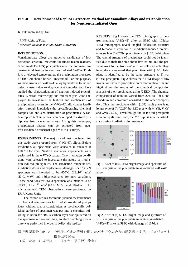
RESULTS: Fig.1 shows the TEM micrographs of neu-
tron-irradiated V-4Cr-4Ti alloy at 593C with 105dpa.
TEM micrographs reveal tangled dislocation structure
and bimodal distribution of irradiation-induced precipi-
tates such as Ti-(CON) precipitate with {100} habit plane.
The crystal structure of precipitates could not be identi-
fied due to their fine size about few ten nm, but the pre-
vious work for neutron-irradiated V-Cr-Ti and V-Ti alloys
have already reported that precipitate with {100} habit
plane is identified to be the same structure as Ti-rich
(CON) precipitate. Fig.2 shows the STEM image of tiny
irradiation-induced precipitate on carbon replica film and
Fig.6 shows the results of the chemical composition
analysis of their precipitates using X-EDX. The chemical
composition of titanium varied from 20% to 100% and
vanadium and chromium consisted of the other composi-
tion. Thus the precipitate with {100} habit plane is no
longer type of Ti-(CON) but MX type with M=(Ti, V, Cr)
and X=(C, O, N). Even though the Ti-(CON) precipitate
is in an equilibrium state, the MX type is in a metastable
state during irradiation circumstance.
0%
20%
40%
60%
80%
100%
Cr
V
Ti
1μ m
Fig.1. A set of (a) STEM bright image and spectrum of
EDS analysis of the precipitate in as received V-4Cr-4Ti
alloo
0%
20%
40%
60%
80%
100%
Cr
V
Ti
0.5μ m
Fig.2. A set of (a) STEM bright image and spectrum of
EDS analysis of the precipitate in neutron -irradiated
V-4Cr-4Ti alloy at 593C with damage of 107dpa.
採択課題番号 24P1-8 中性子・イオン照射を用いたバナジウム合金の熱処理による プロジェクト
損傷回復過程
(福井大院工)福元謙一 (京大・原子炉)徐虫 L

採択課題番号 24P1-9 高温での中性子照射金属中の点欠陥集合体動的挙動と プロジェクト
損傷組織発達過程
(広島国際大学)向田一郎、(愛媛大)山川浩二、(京大原子炉) 義家敏正、徐 虬
Damage Evolution in Neutron-Irradiated Metals during Neutron Irradiation at Elevated Temperatures
I. Mukouda, K. Yamakawa1, T. Yoshiie2 and Q. Xu2
Hiroshima International University 1Faculty of Engineering, Ehime University 2Research Reactor Institute, Kyoto University
INTRODUCTION: Copper and nickel are used as typical FCC metals in radiation damage studies. Many studies have been carried out and reviewed by Singh and Zinkle [1]. They concluded that there is a lack of information on the microstructure of copper and nickel irradiated to below 10-2 dpa at 100 to 300oC [1]. Zinkle and Snead carried out fission neutron irradiation at 230oC to damage levels between 10-2 and 10-1 dpa [2]. They concluded that a high density of small SFT and dislocation loops was observed in copper and nickel, and small voids were observed in irradiated copper. Recently Shimomura and Mukouda carried out fission neutron irradiation of copper at 200 and 300oC at a similar range of dose, we reported dose dependence of voids and SFTs previously. The present work is carried out to examine the evolution of vacancy clusters and voids in neutron-irradiated copper of transient regime at elevated temperatures. To obtain precise results, the irradiation was carried out at the temperature controlled irradiation facility in the KUR.
EXPERIMENTAL PROCEDURES: The specimens used in this study were pure copper and nickel. Specimens were cold-rolled to 0.05 mm and punched out to disks of 3mm in diameter, and annealed in vacuum. Neutron irradiation was carried out in the temperature controlled capsule at KUR reactor in SSS at 1MW. The specimen temperature was kept at 300oC or 200oC during irradiation. After radiation cooling, specimens were electro-polished and using JEOL-2010 TEM at an accelerating voltage of 200kV. Void images were observed by bright field technique of off-Bragg diffraction condition (void contrast) and weak beam dark field (WBDF) image.
RESULTS AND DISCUSSIONS: Figure 1 shows TEM observation of neutron- irradiated copper at 300oC, 5.7 x 10¹⁷ n/cm2, by bright field image. Large voids were seldom observed in this specimen. Fig. 2 shows TEM observation of same specimen by dark field image. Large SFT and small interstitial clusters were observed. The number density of voids and point defect clusters were smaller than irradiation at 5MW 300oC specimen [3]. Fast neutron flux was 1.7 x 10¹³ at 5MW, 3.4 x 10¹² n/cm2s. Another irradiation conditions are progressing now.
REFERENCES [1] B. N. Singh and S. J. Zinkle, J. Nucl. Mater., 206, 212 (1993). [2] S. J. Zinkle and L. L. Snead, J. Nucl. Mater., 225, 123 (1995). [3] I. Mukouda and Y. Shimomura, Mat. Res. Soc. Symp. Proc., 650, R3.11.1-R3.11.6 (2001)
KUR 1MW 300oC 47h
KUR 1MW 300oC 47h
Fig. 1. TEM observation of neutron- irradiated copper at 300oC, 5.7 x 10¹⁷ n/cm2, by bright
field image.
Fig. 2. TEM observation of neutron- irradiated copper at 300oC, 5.7 x 10¹⁷ n/cm2, by dark
field image, (g,5g) g=200.
PR1-9
PR1-10 Positron Annihilation Behavior of Fe-Cr Alloys after Neutron Irradiation in KUR
R. Kasada, K. Sato1, Q. Xu1 and T. Yoshiie1
Institute of Advanced Energy, Kyoto University 1Research Reactor Institute, Kyoto University
INTRODUCTION: Ferritic steels containing Cr are expected to be used for the first-wall component in the fusion reactors as well as the fuel pin cladding in the Generation IV nuclear fission systems [1]. However, high-Cr steels may suffer from thermal aging embrittle-ment, which is well-known 475 °C embrittlement. This is mainly due to phase separation of Fe and Cr as shown in the phase diagram (Fig.1). In the previous study [2], we applied a positron annihilation spectrometry to detect the phase separation in the Fe-Cr alloys under “the Strategic Promotion Program for Basic Nuclear Research by the Ministry of Education, Culture, Sports, Science and Technology of Japan”.
The present collaborative research has moved to in-vestigate the neutron irradiation effect on the phase sep-aration of Fe-Cr ferritic alloys. In the FY2012 we have obtained the first result of positron annihilation study on the Fe-Cr binary alloys before and after the neutron irra-diation in KUR.
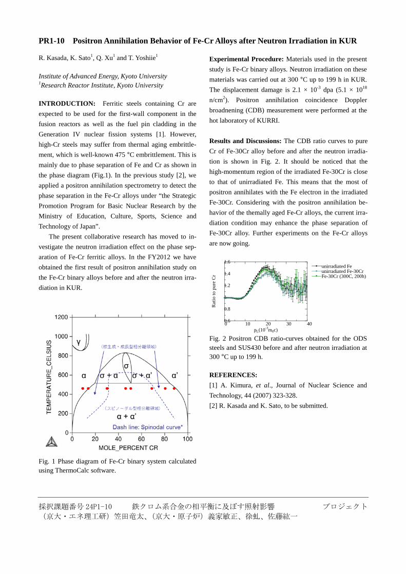
Fig. 1 Phase diagram of Fe-Cr binary system calculated using ThermoCalc software.
Experimental Procedure: Materials used in the present study is Fe-Cr binary alloys. Neutron irradiation on these materials was carried out at 300 °C up to 199 h in KUR. The displacement damage is 2.1 × 10⁻³ dpa (5.1 × 10¹⁸ n/cm2). Positron annihilation coincidence Doppler broadnening (CDB) measurement were performed at the hot laboratory of KURRI.
Results and Discussions: The CDB ratio curves to pure Cr of Fe-30Cr alloy before and after the neutron irradia-tion is shown in Fig. 2. It should be noticed that the high-momentum region of the irradiated Fe-30Cr is close to that of unirradiated Fe. This means that the most of positron annihilates with the Fe electron in the irradiated Fe-30Cr. Considering with the positron annihilation be-havior of the themally aged Fe-Cr alloys, the current irra-diation condition may enhance the phase separation of Fe-30Cr alloy. Further experiments on the Fe-Cr alloys are now going.
0 10 20 30 400.6
0.8
1
1.2
1.4
1.6
pL(10-3m0c)
Rat
io to
pur
e C
r
unirradiated Feunirradiated Fe-30CrFe-30Cr (300C, 200h)
Fig. 2 Positron CDB ratio-curves obtained for the ODS steels and SUS430 before and after neutron irradiation at 300 °C up to 199 h.
REFERENCES: [1] A. Kimura, et al., Journal of Nuclear Science and Technology, 44 (2007) 323-328. [2] R. Kasada and K. Sato, to be submitted.
採択課題番号 24P1-10 鉄クロム系合金の相平衡に及ぼす照射影響 プロジェクト
(京大・エネ理工研)笠田竜太、(京大・原子炉)義家敏正、徐虬、佐藤紘一
PR1-11 Similarity of Radiation Resistance of Nanocrystalline Ni by Ion and Neutron Irradiation
H. Tsuchida, A. Itoh1, K. Sato2, T. Yoshiie2 and Q. Xu2
Quantum Science and Engineering Center, Kyoto Uni-versity 1Depertment of Nuclear Engineering, Kyoto University 2Research Reactor Institute, Kyoto University
INTRODUCTION: Nanocrystalline (NC) materials are known to have high resistance to radiation damage effects, because the grain boundaries act as effective sinks that absorb radiation-induced defects. Up to the present, we have studied radiation damage in NC nickel under ion or neutron irradiation using positron annihila-tion spectroscopy. In the ion irradiation study, we inves-tigated the dependence of the grain size on the formation of transient vacancy defects that occurred during irradia-tion in a real-time measurement of Doppler-broadening positron-annihilation spectroscopy [1]. It was found that the transient vacancies were unstable in NC materials and they could be annihilated at grain boundaries or via re-combination with freely migrating interstitials during irradiation. In the neutron irradiation study, we investi-gated the grain size dependence on defect accumulation using positron annihilation lifetime spectroscopy. The results showed that for NC materials the defect accumu-lation is suppressed, whereas for coarse-grained materials, the defect accumulation or defect clustering is occurred with increasing the neutron fluence. These results suggest that grain boundaries play an important role in the mechanism of radiation resistance in NC materials. In this work, we studied similarity of radiation re-
sistance of NC Ni, in comparison between ion and neu-tron irradiation. It was found that defect accumulation near grain boundaries is suppressed both for ion and neu-tron irradiation.
EXPERIMENTS: An NC Ni, obtained from the Goodfellow Company, UK, was used as a specimen. The average grain size was 30 nm. The specimens were irra-diated with neutron at the dpa 3.8 x 10⁻⁵-1.8 x 10⁻³. Va-cancy defects produced in the irradiated specimens were analyzed by positron annihilation lifetime spectroscopy. We also performed irradiation experiments with high-energy heavy ions. To measure vacancy defects produced during irradiation, the specimens were analyzed by in situ Doppler-broadening positron-annihilation spec-troscopy.
RESULTS: We studied a change in microstructure NC Ni for neutron irradiation, and measured values of posi-tron annihilation lifetime as a function of the dpa. We found that the value of the lifetime, corresponding to the positron annihilation occurring near grain boundaries, remain unchanged with increasing the dpa. This indicates
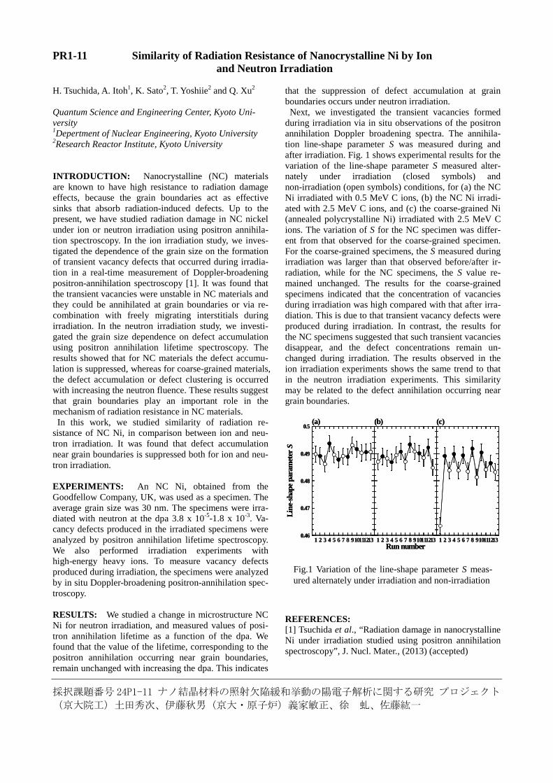
that the suppression of defect accumulation at grain boundaries occurs under neutron irradiation. Next, we investigated the transient vacancies formed during irradiation via in situ observations of the positron annihilation Doppler broadening spectra. The annihila-tion line-shape parameter S was measured during and after irradiation. Fig. 1 shows experimental results for the variation of the line-shape parameter S measured alter-nately under irradiation (closed symbols) and non-irradiation (open symbols) conditions, for (a) the NC Ni irradiated with 0.5 MeV C ions, (b) the NC Ni irradi-ated with 2.5 MeV C ions, and (c) the coarse-grained Ni (annealed polycrystalline Ni) irradiated with 2.5 MeV C ions. The variation of S for the NC specimen was differ-ent from that observed for the coarse-grained specimen. For the coarse-grained specimens, the S measured during irradiation was larger than that observed before/after ir-radiation, while for the NC specimens, the S value re-mained unchanged. The results for the coarse-grained specimens indicated that the concentration of vacancies during irradiation was high compared with that after irra-diation. This is due to that transient vacancy defects were produced during irradiation. In contrast, the results for the NC specimens suggested that such transient vacancies disappear, and the defect concentrations remain un-changed during irradiation. The results observed in the ion irradiation experiments shows the same trend to that in the neutron irradiation experiments. This similarity may be related to the defect annihilation occurring near grain boundaries.
1 2 3 4 5 6 7 8 910111213
(c)
1 2 3 4 5 6 7 8 9101112130.46
0.47
0.48
0.49
0.5
Line
-shap
e par
amet
er S
(a)
1 2 3 4 5 6 7 8 910111213Run number
(b)
1 2 3 4 5 6 7 8 910111213
(c)
1 2 3 4 5 6 7 8 9101112130.46
0.47
0.48
0.49
0.5
Line
-shap
e par
amet
er S
(a)
1 2 3 4 5 6 7 8 910111213Run number
(b)
REFERENCES: [1] Tsuchida et al., “Radiation damage in nanocrystalline Ni under irradiation studied using positron annihilation spectroscopy”, J. Nucl. Mater., (2013) (accepted)
採択課題番号 24P1-11 ナノ結晶材料の照射欠陥緩和挙動の陽電子解析に関する研究 プロジェクト
(京大院工)土田秀次、伊藤秋男(京大・原子炉)義家敏正、徐 虬、佐藤紘一
Fig.1 Variation of the line-shape parameter S meas-ured alternately under irradiation and non-irradiation
PR1-12 Interaction between Deuterium and Defects in Tungsten (2)
K. Sato, R. Tamiya1, Q. Xu and T. Yoshiie
Research Reactor Institute, Kyoto University 1Graduate School of Engineering, Kyoto University
INTRODUCTION: In a fusion reactor, plasma-facing materials (PFMs) must withstand the damage produced by hydrogen and helium at up to 10 keV of energy and heat loads from the plasma, in addition, the neutrons with high energy, high flux and high fluence similar to the structural components. Hydrogen isotopes retain in va-cancy-type defects in PFMs, and this is a critical problem for fusion reactors. To know the interaction between va-cancy-type defects and hydrogen isotopes is very im-portant. In this study, the size and density of vacan-cy-type defects in tungsten was obtained by positron an-nihilation lifetime (PAL) measurements. Next, thermal desorption spectra of deuterium was obtained after deu-terium charging. From these results, trapping site and dissociation energy of deuterium were identified.
EXPERIMENTS: The samples were 99.95% pure tungsten (A.L.M.T. Corp.). The 0.2-mm-thick sheet was punched to 5mm in diameter. These samples were an-nealed at 1773 K for 1 h in a vacuum of less than 10−4 Pa. Electron and deuterium ion irradiations were carried out to introduce defects. Electron irradiation was performed at Electron Linear Accelerator of Research Reactor Insti-tute, Kyoto University. 8 MeV electrons were irradiated up to 9.4×10¹⁷ /cm2 (1.3×10⁻⁴ dpa). A displacement threshold energy used for irradiation dose calculation was 42 eV [1]. Deuterium ion irradiation was performed at Low-energy ion irradiation system of Research Reactor Institute, Kyoto University. 5 keV D2
+ ions were irradi-ated up to 1.0×10¹⁸ /cm2 (20 dpa at defect peak) at room temperature (R.T.). Iron ion irradiation was performed at 2.0-MV tandem accelerator of Quantum Science and En-gineering Center, Kyoto University. 6 MeV Fe3+ ions were irradiated up to 2.3×10¹⁹ /cm2 (8.4 dpa at defect peak) at 573 K. After that, 1 keV D2
+ ions, which do not form irradiation defects, were implanted by low-energy ion irradiation system. Thermal desorption spectroscopy was carried out from R.T. to 1523 K in order to detect elimination behavior of deuterium from tungsten.
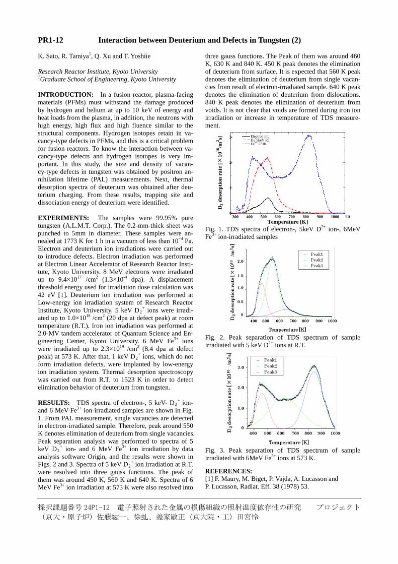
RESULTS: TDS spectra of electron-, 5 keV- D2+ ion-
and 6 MeV-Fe3+ ion-irradiated samples are shown in Fig. 1. From PAL measurement, single vacancies are detectedin electron-irradiated sample. Therefore, peak around 550 K denotes elimination of deuterium from single vacancies. Peak separation analysis was performed to spectra of 5 keV D2
+ ion- and 6 MeV Fe3+ ion irradiation by data analysis software Origin, and the results were shown in Figs. 2 and 3. Spectra of 5 keV D2
+ ion irradiation at R.T. were resolved into three gauss functions. The peak of them was around 450 K, 560 K and 640 K. Spectra of 6 MeV Fe3+ ion irradiation at 573 K were also resolved into
three gauss functions. The Peak of them was around 460 K, 630 K and 840 K. 450 K peak denotes the elimination of deuterium from surface. It is expected that 560 K peak denotes the elimination of deuterium from single vacan-cies from result of electron-irradiated sample. 640 K peak denotes the elimination of deuterium from dislocations. 840 K peak denotes the elimination of deuterium from voids. It is not clear that voids are formed during iron ion irradiation or increase in temperature of TDS measure-ment.
300 400 500 600 700 800 900 1000 1100
1
2
3 Electron irr. D2
+5keV RT Fe3+ 573K
D2 d
esor
ptio
n ra
te [×
1016
/m2 s]
Temperature [K]Fig. 1. TDS spectra of electron-, 5keV D2+ ion-, 6MeV Fe3+ ion-irradiated samples
Fig. 2. Peak separation of TDS spectrum of sample irradiated with 5 keV D2+ ions at R.T.
Fig. 3. Peak separation of TDS spectrum of sample irradiated with 6MeV Fe3+ ions at 573 K.
REFERENCES: [1] F. Maury, M. Biget, P. Vajda, A. Lucasson and P. Lucasson, Radiat. Eff. 38 (1978) 53.
採択課題番号 24P1-12 電子照射された金属の損傷組織の照射温度依存性の研究 プロジェクト
(京大・原子炉)佐藤紘一、徐虬、義家敏正(京大院・工)田宮怜
採択課題番号 24P1-13 高融点金属材料の高温下における応力負荷特性に及ぼす照射効果 プロジェクト
(九大・応力研)徳永 和俊、荒木 邦明(九大・総理工)浮田 天志
(京大・原子炉)徐 虬、義家 敏正
Irradiation Effects on Stress Loading Property of Refractory Metal
at High Temperature
K. Tokunaga, K. Araki, T, Ukita1,
Q. Xu2 andT. Yoshiie
2
Institute for Applied Mechanics, Kyushu University 1Interdisciplinary Graduate School of Engineering
Sciences, Kyushu University 2Research Reactor Institute, Kyoto University
INTRODUCTION: Tungsten (W) is the primary can-
didate for use as plasma facing materials/components
(PFM/PFC). PFM/PFC will be subjected to heavy
thermal loads in the steady state or transient mode com-
bined with high energy neutron irradiation that will cause
serious material degradation. It is necessary to clarify
mechanical strength to evaluate thermal behaviour of
tungsten materials by high heat loading. In the present
works, the tensile testing of W material has been per-
formed up to at 1600 oC to obtain stress-strain curves. In
addition, thermo elasto-plastic stress analyses of W
specimen have been carried out to evaluate modification
of the W specimen exposed to high heat loading. Fur-
thermore, the calculated results have been compared to
surface modification of W specimen under cyclic thermal
loading experiments using an electron beam to evaluate
thermo-mechanical performance of W.
EXPERIMENTS: W material used in the present work
was ITER grade W. Tensile testing was performed on
dog-bone shaped tensile test specimens with an overall
length of 16 mm, a gauge length of 5 mm and an effec-
tive cross section of 0.6 mm2. The orientation of the
specimens used were parallel (L-R type) and perpendicu-
lar (T-R type) directions to rolling direction along rolling
surface, respectively. The tests were conducted at RT, 200,
400, 650, 800, 1000, 1300, 1600 oC. The tests were per-
formed at a strain rate of 2 x10⁻⁴
s-1
. In addition, ITER
grade W was machined to the dimensions of 10 mm x 10
mm x 1mm, followed by mechanical and electro polish-
ing. The polished specimens were subjected to high
heat load experiments by an electron beam irradiation test
simulator. The experiments were conducted at the irradia-
tion conditions; repeated irradiations of 2 s-irradiation
and 7.5 s-rest with one cycle of 9.5 s for totally 200 times.
The surface temperature of the specimens changes from
below 450oC to 1300
oC by 2 s-irradiation. Before and
after the irradiation, the specimen surfaces were exam-
ined by SEM. The thermo elasto-plastic stress analyses
using a transient finite element analyses (FEA) have been
performed to evaluate the thermal behaviour and surface
modification of the W specimens during the high heat
loading experiments. Stress-strain curves of ITER grade
W have been obtained by the tensile testing used in the
FEA.
RESULTS: Figure 1 shows stress-strain curves of
ITER grade W (L-R type) with various temperatures.
Brittle fracture occurs both L-R and T-R type specimens
at RT. On the other hand, ductile fracture occurs on L-R
type specimen but not T-R type specimen at 200 oC. This
result means that DBTT of the specimen is around at 200 oC in the case of the strain rate. Yield strength decreases
and total elongation increases with increasing test tem-
perature. There is difference of about 100 MPa between
L-R and T-R type specimens on tensile strength at RT and
200 oC, however, there is no difference between them
above 400 oC. The reason for this is considered that mi-
gration of dislocation do not occurs at low temperature,
and shape of grain boundary for direction of stress influ-
ences tensile strength. On the other hand, there is differ-
ence between L-R and T-R type specimens on total elon-
gation, even if high temperature which ductile fracture
occurs, and total elongation of L-R type specimen is
higher than that of T-R type specimen. The repeated
heating by electron beam irradiations of 20 times caused
surface roughening in the intragranular. The subsequent
repeated irradiations of totally 200 times caused signifi-
cant surface roughening, cracking in the intragranular and
grain boundaries and surface exfoliation. The FEA in-
dicated that compressive stress is generated in the elec-
tron beam irradiated area during the electron beam irradi-
ation. On the other hand, tensile stress is generated during
cooling after the irradiation of the electron bean is ended.
In addition, plastic deformation occurs and residual stress
remains in the W specimen. Those results suggest that the
surface roughening is considered to be caused due to
plastic deformation by the thermal stresses. Irradiation
effect for stress loading property is planning to be inves-
tigated in the next stage.
Fig. 1 Stress-strain curves of ITER grade
W (LT-R type) with various temperatures.
PR1-13
PR1-14 Effect of Substrate Temperature in Nanocell Fabrication of GaSb*
N. Nitta, K. Yokoyama and M. Taniwaki
Department of Environmental Systems Engineering, Ko-chi University of Technology
INTRODUCTION The authors proposed a novel nanofabrication tech-nique and have performed to fabricate nanocell lattices by focused ion beam (FIB) at room temperature. In their past studies, mainly the possible range of the cell interval and ion dose yielding ordered nanocell lattices has been obtained only at room temperature. However, the mobility of the point defects, which dominates the nanocell formation, depends strongly on the tempera-ture, then, the range of the parameters for successful nanocell formation must differ so much by substrate temperature. Then, in this work, the authors investi-gated the effect of the substrate temperature by fabri-cating nanocell lattices on GaSb (100) surface at room temperature and at lower temperature (130 K) and comparing them.
EXPERIMENT Nanocell lattices were fabricated using FIB Quanta 3D 200i by the nanofabrication technique that the authors had proposed. In order to know the possible range of the cell interval for the ordered nanocell lattice, an initial pattern consisting of nine matrices with a dif-ferent void interval was created by the same ion dose per one dot in box repairing mode of the FIB with 30 keV Ga+ and it was developed by a constant ion dose per unit area in the image scanning mode of the same FIB. Such processes were performed in variations of initial ion dose and developing ion dose at room tem-perature and 130 K. The ion doses per one dot in the initial procedure were 1.13×10⁴ - 2.25×10⁶ ions/dot and the ion doses per unit area in the second procedure were 1.6×10¹³ - 2.9×10¹⁴ ions/cm2. The change of the pattern during irradiation was observed in situ by FIB secondary electron image.
RESULTS The lattice image of the pattern at 130K is observed obscurely, which may be due to the gas adsorption on the surface. The dot contrast is bright on the sample fabricated at 130K in contrast to the dark image on the sample at room temperature. The bright contrast means the elevation of the surface. This is due to the low migration of vacancies at cryogenic temperature, which retards the growth of void comparing at room temperature and then the top surfaces of the voids were not yet completely removed. The ordered im-age at 130 K was observed in the dot interval of 80 nm which was not made at room temperature. The devel-opment of the pattern by scanning at 130 K was re-
tarded comparing at room temperature, which is again attributed to the difference in the migration of point defects, especially vacancies. The cell diameter in one scanned pattern was larger in larger dot interval, and 55 – 108 nm at 130 K and 90 – 125 nm at room temperature. It increased monotonously with in-creasing scan times in every lattice at both tempera-tures, though it saturated to a critical value a little less than its dot interval. However, some difference is observed between two substrate temperatures; the curve of cell diameter against scan times is a convex below at 130 K, and linear or a convex on the top at room temperature. The increasing rate of the diameter to scan times at early scanning stage is 7.8 nm/one scan at 140 K and 13.7 nm/one scan at room tempera-ture. We consider that this difference may be caused by the difference of the nanocell development mecha-nisms (probably it contains two elementary mecha-nism at least) between at room temperature and at cryogenic temperature. This detailed understanding is our future issue.
CONCLUSION The nanocell fabrication experiment on GaSb (100) using 30 keV Ga+ at room temperature is summarized as follows. The appropriate ion dose for fabrication of the initial void is 1.13 – 2.25×10⁵ ions/dot, and nano-cell lattice with 80 – 300 nm dot interval is achieved.The nanocell fabrication on GaSb surface at low temperature has several advantages over that at room temperature. One is to suppress the secondary void formation. In the case of 130 K, secondary voids formed first by 8 scans, though they formed by 5 scans at room temperature and their size was smaller at 130 K. Another advantage at low temperature is to create the ordered nanocell lattice with smaller dot interval. Nanocell formation mechanism at cryogenic temperature is somewhat different from that at room temperature. Fabrication at low temperature has some advantages in application, that is, nanocell lat-tices are easily obtained in wider range of dot interval, without secondary void formation.
*This report is summarized from “Nanocell fabricationon GaSb at room temperature and cryogenic tempera-ture (N. Nitta, K. Yokoyama, and M. Taniwaki, AIP conf. Proc. 1496)
採択課題番号 24P1-14 半導体イオン照射によって導入される点欠陥挙動の解明と プロジェクト
ナノセル技術の開発
(高知工科大)谷脇雅文,新田紀子 (京大原子炉)義家敏正,徐 虬
PR1-15 Deuterium Retention in Electron-Irradiated VPS-W
Y. Hatano, J. Shi, T. Nozaki, K. Masuda, T. Tokunaga1, H. Watanabe1, N. Yoshida1, K. Sato2 and Q. Xu2
Hydrogen Isotope Research Center, University of To-yama 1Research Institute for Applied Mechanics, Kyushu University 2Research Reactor Institute, Kyoto University
INTRODUCTION: Tungsten (W) is currently recog-nized as a primary candidate of plasma-facing material (PFM) for future fusion reactors. Vacuum plasma spray-ing is a technique to prepare W layers on structural mate-rials such as reduced-activation ferritic/martensitic steels. Tritium (T) is the radioisotope of hydrogen and used as fuel in fusion reactors together with deuterium (D). The fusion reaction of D and T forms 3.5 MeV He and 14 MeV neutrons. PFMs are subjected to irradiation of those high energy neutrons. Therefore, understanding of T re-tention in PFMs and effects of neutron irradiation is im-portant issue for assessing safety margins of fusion reac-tors. Indeed, significant increase in D retention with neu-tron irradiation has been observed for bulk W fabricated by powder metallurgy in Japan–US Joint Research Pro-ject TITAN [1–2]. From these viewpoints, effects of dis-placement damages on D retention in VPS-W were ex-amined in this study with irradiation of 8 MeV electrons. High energy electrons induce defects throughout the thickness of materials like neutrons, while ions form de-fects only in a shallow region beneath the surface.
EXPERIMENTS: The specimens used were VPS-W layers (0.6 mm thickness) prepared on car-bon/carbon-fiber composite (CFC, CX-2002U) by Plan-see Aktiengesllshaft. After removing CFC substrates by mechanical polishing, the VPS-W layers were exposed to D2 gas in a high-vacuum device at 100 kPa and 673 K for 10 hours under the following conditions:
(1) As-received, (2) After heating in vacuum at 1273 K for 1.5 hours, (3) After irradiation with 8 MeV electrons up to 10−3
displacement per atom (dpa) following the above-mentioned heat treatment in vacuum.
Exposure to D2 gas under several different conditions showed that the specimens were saturated with D under the above-mentioned conditions. The D retention was measured by thermal desorption spectroscopy (TDS) at the temperature ramp rate of 0.5 K s−1. Desorption spec-tra were simulated with the program TMAP4 [3].
RESULTS: The retention of D in VPS-W layer under as-received conditions was 1 × 10⁻⁵ in atomic ratio, [D]/[W]. It decreased to [D]/[W] = 1 × 10⁻⁶ by the heat treatment in vacuum at 1273 K. During the heat treatment,
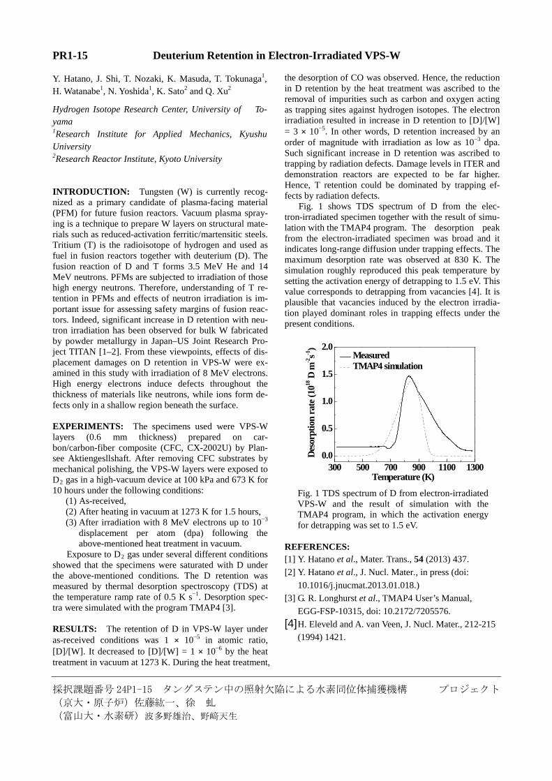
the desorption of CO was observed. Hence, the reduction in D retention by the heat treatment was ascribed to the removal of impurities such as carbon and oxygen acting as trapping sites against hydrogen isotopes. The electron irradiation resulted in increase in D retention to [D]/[W] = 3 × 10⁻⁵. In other words, D retention increased by an order of magnitude with irradiation as low as 10−3 dpa. Such significant increase in D retention was ascribed to trapping by radiation defects. Damage levels in ITER and demonstration reactors are expected to be far higher. Hence, T retention could be dominated by trapping ef-fects by radiation defects. Fig. 1 shows TDS spectrum of D from the elec-tron-irradiated specimen together with the result of simu-lation with the TMAP4 program. The desorption peak from the electron-irradiated specimen was broad and it indicates long-range diffusion under trapping effects. The maximum desorption rate was observed at 830 K. The simulation roughly reproduced this peak temperature by setting the activation energy of detrapping to 1.5 eV. This value corresponds to detrapping from vacancies [4]. It is plausible that vacancies induced by the electron irradia-tion played dominant roles in trapping effects under the present conditions.
300 500 700 900 1100 13000.0
0.5
1.0
1.5
2.0 Measured TMAP4 simulation
Deso
rptio
n ra
te (1
018 D
m-2s-1
)
Temperature (K)
Fig. 1 TDS spectrum of D from electron-irradiated VPS-W and the result of simulation with the TMAP4 program, in which the activation energy for detrapping was set to 1.5 eV.
REFERENCES: [1] Y. Hatano et al., Mater. Trans., 54 (2013) 437. [2] Y. Hatano et al., J. Nucl. Mater., in press (doi:
10.1016/j.jnucmat.2013.01.018.) [3] G. R. Longhurst et al., TMAP4 User’s Manual,
EGG-FSP-10315, doi: 10.2172/7205576. [4] H. Eleveld and A. van Veen, J. Nucl. Mater., 212-215
(1994) 1421.
採択課題番号 24P1-15 タングステン中の照射欠陥による水素同位体捕獲機構 プロジェクト
(京大・原子炉)佐藤紘一、徐 虬
(富山大・水素研)波多野雄治、野﨑天生