Embed Size (px)
Citation preview

www.bookspar.com | Website for students | VTU NOTES
COMPUTER ORGANISATIONCHAPTER – 1
BASIC STRUCTURE OF COMPUTERS
Computer types: -
A computer can be defined as a fast electronic calculating machine that accepts the (data) digitized input information process it as per the list of internally stored instructions and produces the resulting information.
List of instructions are called programs & internal storage is called computer memory.
The different types of computers are1. Personal computers: - This is the most common type found in homes, schools,
Business offices etc., It is the most common type of desk top computers with processing and storage units along with various input and output devices.
2. Note book computers: - These are compact and portable versions of PC3. Work stations: - These have high resolution input/output (I/O) graphics
capability, but with same dimensions as that of desktop computer. These are used in engineering applications of interactive design work.
4. Enterprise systems: - These are used for business data processing in medium to large corporations that require much more computing power and storage capacity than work stations. Internet associated with servers have become a dominant worldwide source of all types of information.
5. Super computers: - These are used for large scale numerical calculations required in the applications like weather forecasting etc.,
Functional unit: - A computer consists of five functionally independent main parts input, memory,
arithmetic logic unit (ALU), output and control unit.
www.bookspar.com | Website for students | VTU NOTES 1
I/O Processor Memory
Input
Output
ALU
Control Unit

www.bookspar.com | Website for students | VTU NOTESFig a : Functional units of computer
Input device accepts the coded information as source program i.e. high level language. This is either stored in the memory or immediately used by the processor to perform the desired operations. The program stored in the memory determines the processing steps. Basically the computer converts one source program to an object program. i.e. into machine language.
Finally the results are sent to the outside world through output device. All of these actions are coordinated by the control unit.
Input unit: - The source program/high level language program/coded information/simply data
is fed to a computer through input devices keyboard is a most common type. Whenever a key is pressed, one corresponding word or number is translated into its equivalent binary code over a cable & fed either to memory or processor.
Joysticks, trackballs, mouse, scanners etc are other input devices.
Memory unit: - Its function into store programs and data. It is basically to two types
1. Primary memory2. Secondary memory
1. Primary memory: - Is the one exclusively associated with the processor and operates at the electronics speeds programs must be stored in this memory while they are being executed. The memory contains a large number of semiconductors storage cells. Each capable of storing one bit of information. These are processed in a group of fixed site called word.
To provide easy access to a word in memory, a distinct address is associated with
each word location. Addresses are numbers that identify memory location.
Number of bits in each word is called word length of the computer. Programs must reside in the memory during execution. Instructions and data can be written into the memory or read out under the control of processor.
Memory in which any location can be reached in a short and fixed amount of time after specifying its address is called random-access memory (RAM).
The time required to access one word in called memory access time. Memory which is only readable by the user and contents of which can’t be altered is called read only memory (ROM) it contains operating system.
Caches are the small fast RAM units, which are coupled with the processor and are aften contained on the same IC chip to achieve high performance. Although primary storage is essential it tends to be expensive.
www.bookspar.com | Website for students | VTU NOTES 2

www.bookspar.com | Website for students | VTU NOTES2 Secondary memory: - Is used where large amounts of data & programs have to be stored, particularly information that is accessed infrequently.
Examples: - Magnetic disks & tapes, optical disks (ie CD-ROM’s), floppies etc.,
Arithmetic logic unit (ALU):- Most of the computer operators are executed in ALU of the processor like
addition, subtraction, division, multiplication, etc. the operands are brought into the ALU from memory and stored in high speed storage elements called register. Then according to the instructions the operation is performed in the required sequence.
The control and the ALU are may times faster than other devices connected to a computer system. This enables a single processor to control a number of external devices such as key boards, displays, magnetic and optical disks, sensors and other mechanical controllers.
Output unit:- These actually are the counterparts of input unit. Its basic function is to send the
processed results to the outside world.
Examples:- Printer, speakers, monitor etc.
Control unit:- It effectively is the nerve center that sends signals to other units and senses their
states. The actual timing signals that govern the transfer of data between input unit, processor, memory and output unit are generated by the control unit.
Basic operational concepts: - To perform a given task an appropriate program consisting of a list of
instructions is stored in the memory. Individual instructions are brought from the memory into the processor, which executes the specified operations. Data to be stored are also stored in the memory.
Examples: - Add LOCA, R0
This instruction adds the operand at memory location LOCA, to operand in register R0 & places the sum into register. This instruction requires the performance of several steps,
1. First the instruction is fetched from the memory into the processor.2. The operand at LOCA is fetched and added to the contents of R0
3. Finally the resulting sum is stored in the register R0
The preceding add instruction combines a memory access operation with an ALUOperations. In some other type of computers, these two types of operations are performed by separate instructions for performance reasons.
Load LOCA, R1Add R1, R0
www.bookspar.com | Website for students | VTU NOTES 3

www.bookspar.com | Website for students | VTU NOTES Transfers between the memory and the processor are started by sending the
address of the memory location to be accessed to the memory unit and issuing the appropriate control signals. The data are then transferred to or from the memory.
Fig b : Connections between the processor and the memory
The fig shows how memory & the processor can be connected. In addition to the ALU & the control circuitry, the processor contains a number of registers used for several different purposes.
The instruction register (IR):- Holds the instructions that is currently being executed. Its output is available for the control circuits which generates the timing signals that control the various processing elements in one execution of instruction.
The program counter PC:- This is another specialized register that keeps track of execution of a program. It
contains the memory address of the next instruction to be fetched and executed.
Besides IR and PC, there are n-general purpose registers R0 through Rn-1.The other two registers which facilitate communication with memory are: -
1. MAR – (Memory Address Register):- It holds the address of the location to be accessed.
www.bookspar.com | Website for students | VTU NOTES 4
n- GPRs
MEMORY
MAR
PC
IR
MDR CONTROL
ALU
R0 R1 … … … …
Rn-1

www.bookspar.com | Website for students | VTU NOTES2. MDR – (Memory Data Register):- It contains the data to be written into or read
out of the address location.
Operating steps are1. Programs reside in the memory & usually get these through the I/P unit.2. Execution of the program starts when the PC is set to point at the first instruction
of the program.3. Contents of PC are transferred to MAR and a Read Control Signal is sent to the
memory.4. After the time required to access the memory elapses, the address word is read out
of the memory and loaded into the MDR.5. Now contents of MDR are transferred to the IR & now the instruction is ready to
be decoded and executed.6. If the instruction involves an operation by the ALU, it is necessary to obtain the
required operands.7. An operand in the memory is fetched by sending its address to MAR & Initiating
a read cycle.8. When the operand has been read from the memory to the MDR, it is transferred
from MDR to the ALU.9. After one or two such repeated cycles, the ALU can perform the desired
operation.10. If the result of this operation is to be stored in the memory, the result is sent to
MDR.11. Address of location where the result is stored is sent to MAR & a write cycle is
initiated.12. The contents of PC are incremented so that PC points to the next instruction that
is to be executed.
Normal execution of a program may be preempted (temporarily interrupted) if some devices require urgent servicing, to do this one device raises an Interrupt signal.
An interrupt is a request signal from an I/O device for service by the processor. The processor provides the requested service by executing an appropriate interrupt service routine.
The Diversion may change the internal stage of the processor its state must be saved in the memory location before interruption. When the interrupt-routine service is completed the state of the processor is restored so that the interrupted program may continue.
Bus structure: - The simplest and most common way of interconnecting various parts of the
computer. To achieve a reasonable speed of operation, a computer must be organized so that
all its units can handle one full word of data at a given time.
www.bookspar.com | Website for students | VTU NOTES 5

www.bookspar.com | Website for students | VTU NOTES A group of lines that serve as a connecting port for several devices is called a
bus. In addition to the lines that carry the data, the bus must have lines for address and
control purpose.
Simplest way to interconnect is to use the single bus as shown
Fig c: Single bus structure
Since the bus can be used for only one transfer at a time, only two units can actively use the bus at any given time. Bus control lines are used to arbitrate multiple requests for use of one bus.
Single bus structure is
Low cost Very flexible for attaching peripheral devices
Multiple bus structure certainly increases, the performance but also increases the cost significantly.
All the interconnected devices are not of same speed & time, leads to a bit of a problem. This is solved by using cache registers (ie buffer registers). These buffers are electronic registers of small capacity when compared to the main memory but of comparable speed.
The instructions from the processor at once are loaded into these buffers and then the complete transfer of data at a fast rate will take place.
Performance: - The most important measure of the performance of a computer is how quickly it
can execute programs. The speed with which a computer executes program is affected by
www.bookspar.com | Website for students | VTU NOTES 6
INPUT MEMORY PROCESSOR OUTPUT

www.bookspar.com | Website for students | VTU NOTESthe design of its hardware. For best performance, it is necessary to design the compiles, the machine instruction set, and the hardware in a coordinated way.
The total time required to execute the program is elapsed time is a measure of the performance of the entire computer system. It is affected by the speed of the processor, the disk and the printer. The time needed to execute a instruction is called the processor time.
Just as the elapsed time for the execution of a program depends on all units in a computer system, the processor time depends on the hardware involved in the execution of individual machine instructions. This hardware comprises the processor and the memory which are usually connected by the bus as shown in the fig c.
Bus
Fig d :The processor cache
The pertinent parts of the fig. c is repeated in fig. d which includes the cache memory as part of the processor unit.
Let us examine the flow of program instructions and data between the memory and the processor. At the start of execution, all program instructions and the required data are stored in the main memory. As the execution proceeds, instructions are fetched one by one over the bus into the processor, and a copy is placed in the cache later if the same instruction or data item is needed a second time, it is read directly from the cache.
The processor and relatively small cache memory can be fabricated on a single IC chip. The internal speed of performing the basic steps of instruction processing on chip is very high and is considerably faster than the speed at which the instruction and data can be fetched from the main memory. A program will be executed faster if the movement of instructions and data between the main memory and the processor is minimized, which is achieved by using the cache.
For example:- Suppose a number of instructions are executed repeatedly over a short period of time as happens in a program loop. If these instructions are available in the cache, they can be fetched quickly during the period of repeated use. The same applies to the data that are used repeatedly.
Processor clock: -
www.bookspar.com | Website for students | VTU NOTES 7
Main Memory
Processor Cache Memory

www.bookspar.com | Website for students | VTU NOTES Processor circuits are controlled by a timing signal called clock. The clock
designer the regular time intervals called clock cycles. To execute a machine instruction the processor divides the action to be performed into a sequence of basic steps that each step can be completed in one clock cycle. The length P of one clock cycle is an important parameter that affects the processor performance.
Processor used in today’s personal computer and work station have a clock rates that range from a few hundred million to over a billion cycles per second.
Basic performance equation: - We now focus our attention on the processor time component of the total elapsed
time. Let ‘T’ be the processor time required to execute a program that has been prepared in some high-level language. The compiler generates a machine language object program that corresponds to the source program. Assume that complete execution of the program requires the execution of N machine cycle language instructions. The number N is the actual number of instruction execution and is not necessarily equal to the number of machine cycle instructions in the object program. Some instruction may be executed more than once, which in the case for instructions inside a program loop others may not be executed all, depending on the input data used.
Suppose that the average number of basic steps needed to execute one machine cycle instruction is S, where each basic step is completed in one clock cycle. If clock rate is ‘R’ cycles per second, the program execution time is given by
this is often referred to as the basic performance equation.
We must emphasize that N, S & R are not independent parameters changing one may affect another. Introducing a new feature in the design of a processor will lead to improved performance only if the overall result is to reduce the value of T.
Pipelining and super scalar operation: - We assume that instructions are executed one after the other. Hence the value of
S is the total number of basic steps, or clock cycles, required to execute one instruction. A substantial improvement in performance can be achieved by overlapping the execution of successive instructions using a technique called pipelining.
Consider Add R1 R2 R3
This adds the contents of R1 & R2 and places the sum into R3.
The contents of R1 & R2 are first transferred to the inputs of ALU. After the addition operation is performed, the sum is transferred to R3. The processor can read the next instruction from the memory, while the addition operation is being performed. Then of that instruction also uses, the ALU, its operand can be transferred to the ALU inputs at the same time that the add instructions is being transferred to R3.
www.bookspar.com | Website for students | VTU NOTES 8

www.bookspar.com | Website for students | VTU NOTES In the ideal case if all instructions are overlapped to the maximum degree
possible the execution proceeds at the rate of one instruction completed in each clock cycle. Individual instructions still require several clock cycles to complete. But for the purpose of computing T, effective value of S is 1.
A higher degree of concurrency can be achieved if multiple instructions pipelines are implemented in the processor. This means that multiple functional units are used creating parallel paths through which different instructions can be executed in parallel with such an arrangement, it becomes possible to start the execution of several instructions in every clock cycle. This mode of operation is called superscalar execution. If it can be sustained for a long time during program execution the effective value of S can be reduced to less than one. But the parallel execution must preserve logical correctness of programs, that is the results produced must be same as those produced by the serial execution of program instructions. Now a days may processor are designed in this manner.
Clock rate:- These are two possibilities for increasing the clock rate ‘R’.
1. Improving the IC technology makes logical circuit faster, which reduces the time of execution of basic steps. This allows the clock period P, to be reduced and the clock rate R to be increased.
2. Reducing the amount of processing done in one basic step also makes it possible to reduce the clock period P. however if the actions that have to be performed by an instructions remain the same, the number of basic steps needed may increase.
Increase in the value ‘R’ that are entirely caused by improvements in IC technology affects all aspects of the processor’s operation equally with the exception of the time it takes to access the main memory. In the presence of cache the percentage of accesses to the main memory is small. Hence much of the performance gain excepted from the use of faster technology can be realized.
Instruction set CISC & RISC:- Simple instructions require a small number of basic steps to execute. Complex
instructions involve a large number of steps. For a processor that has only simple instruction a large number of instructions may be needed to perform a given programming task. This could lead to a large value of ‘N’ and a small value of ‘S’ on the other hand if individual instructions perform more complex operations, a fewer instructions will be needed, leading to a lower value of N and a larger value of S. It is not obvious if one choice is better than the other.
But complex instructions combined with pipelining (effective value of S 1) would achieve one best performance. However, it is much easier to implement efficient pipelining in processors with simple instruction sets.
Performance measurements:- It is very important to be able to access the performance of a computer, comp
designers use performance estimates to evaluate the effectiveness of new features.
www.bookspar.com | Website for students | VTU NOTES 9

www.bookspar.com | Website for students | VTU NOTES The previous argument suggests that the performance of a computer is given by
the execution time T, for the program of interest.
Inspite of the performance equation being so simple, the evaluation of ‘T’ is highly complex. Moreover the parameters like the clock speed and various architectural features are not reliable indicators of the expected performance.
Hence measurement of computer performance using bench mark programs is done to make comparisons possible, standardized programs must be used.
The performance measure is the time taken by the computer to execute a given bench mark. Initially some attempts were made to create artificial programs that could be used as bench mark programs. But synthetic programs do not properly predict the performance obtained when real application programs are run.
A non profit organization called SPEC- system performance evaluation corporation selects and publishes bench marks.
The program selected range from game playing, compiler, and data base applications to numerically intensive programs in astrophysics and quantum chemistry. In each case, the program is compiled under test, and the running time on a real computer is measured. The same program is also compiled and run on one computer selected as reference.The ‘SPEC’ rating is computed as follows.
Running time on the reference computer SPEC rating =
Running time on the computer under test
If the SPEC rating = 50
Means that the computer under test is 50 times as fast as the ultra sparc 10. This is repeated for all the programs in the SPEC suit, and the geometric mean of the result is computed.
Let SPECi be the rating for program ‘i’ in the suite. The overall SPEC rating for the computer is given by
SPEC rating =
Where ‘n’ = number of programs in suite.
Since actual execution time is measured the SPEC rating is a measure of the combined effect of all factors affecting performance, including the compiler, the OS, the processor, the memory of comp being tested.
Multiprocessor & microprocessors:-
www.bookspar.com | Website for students | VTU NOTES 10

www.bookspar.com | Website for students | VTU NOTES Large computers that contain a number of processor units are called
multiprocessor system. These systems either execute a number of different application tasks in parallel or
execute subtasks of a single large task in parallel. All processors usually have access to all memory locations in such system &
hence they are called shared memory multiprocessor systems. The high performance of these systems comes with much increased complexity
and cost. In contrast to multiprocessor systems, it is also possible to use an interconnected
group of complete computers to achieve high total computational power. These computers normally have access to their own memory units when the tasks they are executing need to communicate data they do so by exchanging messages over a communication network. This properly distinguishes them from shared memory multiprocessors, leading to name message-passing multi computer.
www.bookspar.com | Website for students | VTU NOTES 11

www.bookspar.com | Website for students | VTU NOTESCOMPUTER ORGANISATION
CHAPTER – 2
Number Representation:- Consider an n-bit vectorB =
Where = 0 or 1 for 0 . This vector can represent unsigned integer values V in the range 0 to -1, where
V(B) = We obviously need to represent both positive and negative numbers. Three systems are used for representing such numbers :
Sign-and-magnitude 1’s-complement 2’s-complement
In all three systems, the leftmost bit is 0 for positive numbers and 1 for negative numbers. Fig 2.1 illustrates all three representations using 4-bit numbers. Positive values have identical representations in al systems, but negative values have different representations. In the sign-and-magnitude systems, negative values are represented by changing the most significant bit (b3 in figure 2.1) from 0 to 1 in the B vector of the corresponding positive value. For example, +5 is represented by 0101, and -5 is represented by 1101. In 1’s-complement representation, negative values are obtained by complementing each bit of the corresponding positive number. Thus, the representation for -3 is obtained by complementing each bit in the vector 0011 to yield 1100. clearly, the same operation, bit complementing, is done in converting a negative number to the corresponding positive value. Converting either way is referred to as forming the 1’s-complement of a given number. Finally, in the 2’s-complement system, forming the 2’s-complement of a number is done by subtracting that number from 2n. B Values represented Sign and
b3b2b1 b0 magnitude1's complement
2's complement
0 1 1 1 +7 +7 +70 1 1 0 +6 +6 +60 1 0 1 +5 +5 +50 1 0 0 +4 +4 +40 0 1 1 +3 +3 +30 0 1 0 +2 +2 +20 0 0 1 +1 +1 +10 0 0 0 +0 +0 +01 0 0 0 -0 -0 -01 0 0 1 -1 -1 -11 0 1 0 -2 -2 -21 0 1 1 -3 -3 -31 1 0 0 -4 -4 -41 1 0 1 -5 -5 -51 1 1 0 -6 -6 -61 1 1 1 -7 -7 -7
Hence, the 2’s complement of a number is obtained by adding 1 to the 1’s complement of that number.
www.bookspar.com | Website for students | VTU NOTES 12

www.bookspar.com | Website for students | VTU NOTESAddition of Positive numbers:-
Consider adding two 1-bit numbers. The results are shown in figure 2.2. Note that the sum of 1 and 1 requires the 2-bit vector 10 to represent the value 2. We say that the sum is 0 and the carry-out is 1. In order to add multiple-bit numbers, we use a method analogous to that used for manual computation with decimal numbers. We add bit pairs starting from the low-order (right) and of the bit vectors, propagating carries toward the high-order (left) end.
0 1 0 1+ 0 + 0 + 1 + 1____ ____ ___ ___ 0 1 1 1 0
Carry-outFigure 2.2 Addition of 1-bit numbers.
MEMORY LOCATIONS AND ADDRESSES:-
Number and character operands, as well as instructions, are stored in the memory of a computer. The memory consists of many millions of storage cells, each of which can store a bit of information having the value 0 or 1. Because a single bit represents a very small amount of information, bits are seldom handled individually. The usual approach is to deal with them in groups of fixed size. For this purpose, the memory is organized so that a group of n bits can be stored or retrieved in a single, basic operation. Each group of n bits is referred to as a word of information, and n is called the word length. The memory of a computer can be schematically represented as a collection of words as shown in figure (a).
Modern computers have word lengths that typically range from 16 to 64 bits. If the word length of a computer is 32 bits, a single word can store a 32-bit 2’s complement number or four ASCII characters, each occupying 8 bits. A unit of 8 bits is called a byte.
Accessing the memory to store or retrieve a single item of information, either a word or a byte, requires distinct names or addresses for each item location. It is customary to use numbers from 0 through 2K-1, for some suitable values of k, as the addresses of successive locations in the memory. The 2k addresses constitute the address space of the computer, and the memory can have up to 2k addressable locations. 24-bit address generates an address space of 224 (16,777,216) locations. A 32-bit address creates an address space of 232 or 4G (4 giga) locations.
BYTE ADDRESSABILITY:- We now have three basic information quantities to deal with: the bit, byte and
word. A byte is always 8 bits, but the word length typically ranges from 16 to 64 bits. The most practical assignment is to have successive addresses refer to successive byte
www.bookspar.com | Website for students | VTU NOTES 13
www.bookspar.com | Website for students | VTU NOTESFig a Memory words
n bits
… … …
… … …
(a) A signed integer
32 bitsb31 b30 ……. b1 b0
Sign bit: b31 = 0 for positive numbers
b32 = 1 for negative numbers
(b) Four characters
8 bits 8 bits 8 bits 8 bits ASCII ASCII ASCII ASCII Character character character character
Locations in the memory. This is the assignment used in most modern computers, and is the one we will normally use in this book. The term byte-addressable memory is use for this assignment. Byte locations have addresses 0,1,2, …. Thus, if the word length of the machine is 32 bits, successive words are located at addresses 0,4,8,…., with each word consisting of four bytes.
BIG-ENDIAN AND LITTLE-ENDIAN ASIGNMENTS:-
www.bookspar.com | Website for students | VTU NOTES 14
First word
Second word
i-th word
Last word

www.bookspar.com | Website for students | VTU NOTES There are two ways that byte addresses can be assigned across words, as shown
in fig b. The name big-endian is used when lower byte addresses are used for the more significant bytes (the leftmost bytes) of the word. The name little-endian is used for the opposite ordering, where the lower byte addresses are used for the less significant bytes (the rightmost bytes) of the word.
In addition to specifying the address ordering of bytes within a word, it is also necessary to specify the labeling of bits within a byte or a word. The same ordering is also used for labeling bits within a byte, that is, b7, b6, …., b0, from left to right.
Word Address Byte address Byte address
0 0
4 4
2k-4 2k-4
(a) Big-endian assignment (b) Little-endian assignment
WORD ALIGNMENT:- In the case of a 32-bit word length, natural word boundaries occur at addresses 0,
4, 8, …, as shown in above fig. We say that the word locations have aligned addresses . in general, words are said to be aligned in memory if they begin at a byte address that is a multiple of the number of bytes in a word. The memory of bytes in a word is a power of 2. Hence, if the word length is 16 (2 bytes), aligned words begin at byte addresses 0,2,4,…, and for a word length of 64 (23 bytes), aligned words begin at bytes addresses 0,8,16 ….
There is no fundamental reason why words cannot begin at an arbitrary byte address. In that case, words are said to have unaligned addresses. While the most common case is to use aligned addresses, some computers allow the use of unaligned word addresses.
ACCESSING NUMBERS, CHARACTERS, AND CHARACTER STRINGS:-
www.bookspar.com | Website for students | VTU NOTES 15
0 1 2 3
4 5 6 7
…. …. ….
2k-4 2k-3 2k-2 2k-1
3 2 1 0
7 6 5 4
…. …. ….
2k-1 2k-2 2k-3 2k-4

www.bookspar.com | Website for students | VTU NOTES A number usually occupies one word. It can be accessed in the memory by
specifying its word address. Similarly, individual characters can be accessed by their byte address.
In many applications, it is necessary to handle character strings of variable length. The beginning of the string is indicated by giving the address of the byte containing its first character. Successive byte locations contain successive characters of the string. There are two ways to indicate the length of the string. A special control character with the meaning “end of string” can be used as the last character in the string, or a separate memory word location or processor register can contain a number indicating the length of the string in bytes.
MEMORY OPERATIONS:- Both program instructions and data operands are stored in the memory. To
execute an instruction, the processor control circuits must cause the word (or words) containing the instruction to be transferred from the memory to the processor. Operands and results must also be moved between the memory and the processor. Thus, two basic operations involving the memory are needed, namely, Load (or Read or Fetch) and Store (or Write).
The load operation transfers a copy of the contents of a specific memory location to the processor. The memory contents remain unchanged. To start a Load operation, the processor sends the address of the desired location to the memory and requests that its contents be read. The memory reads the data stored at that address and sends them to the processor.
The store operation transfers an item of information from the processor to a specific memory location, destroying the former contents of that location. The processor sends the address of the desired location to the memory, together with the data to be written into that location.
An information item of either one word or one byte can be transferred between the processor and the memory in a single operation. Actually this transfer in between the CPU register & main memory.
INSTRUCTIONS AND INSTRUCTION SEQUENCING:- A computer must have instructions capable of performing four types of
operations. Data transfers between the memory and the processor registers Arithmetic and logic operations on data Program sequencing and control I/O transfers
REGISTER TRANSFER NOTATION:- Transfer of information from one location in the computer to another. Possible
locations that may be involved in such transfers are memory locations that may be
www.bookspar.com | Website for students | VTU NOTES 16

www.bookspar.com | Website for students | VTU NOTESinvolved in such transfers are memory locations, processor registers, or registers in the I/O subsystem. Most of the time, we identify a location by a symbolic name standing for its hardware binary address.
Example, names for the addresses of memory locations may be LOC, PLACE, A, VAR2; processor registers names may be R0, R5; and I/O register names may be DATAIN, OUTSTATUS, and so on. The contents of a location are denoted by placing square brackets around the name of the location. Thus, the expression
R1 [LOC]Means that the contents of memory location LOC are transferred into processor register R1.
As another example, consider the operation that adds the contents of registers R1 and R2, and then places their sum into register R3. This action is indicated as
R3 [R1] + [R2]
This type of notation is known as Register Transfer Notation (RTN). Note that the right-hand side of an RTN expression always denotes a value, and the left-hand side is the name of a location where the value is to be places, overwriting the old contents of that location.
ASSEMBLY LANGUAGE NOTATION:- Another type of notation to represent machine instructions and programs. For
this, we use an assembly language format. For example, an instruction that causes the transfer described above, from memory location LOC to processor register R1, is specified by the statement
Move LOC, R1
The contents of LOC are unchanged by the execution of this instruction, but the old contents of register R1 are overwritten.
The second example of adding two numbers contained in processor registers R1 and R2 and placing their sum in R3 can be specified by the assembly language statement
Add R1, R2, R3
BASIC INSTRUCTIONS:- The operation of adding two numbers is a fundamental capability in any
computer. The statementC = A + B
In a high-level language program is a command to the computer to add the current values of the two variables called A and B, and to assign the sum to a third variable, C. When the program containing this statement is compiled, the three variables, A, B, and C, are assigned to distinct locations in the memory. We will use the variable names to refer to the corresponding memory location addresses. The contents of these locations represent the values of the three variables. Hence, the above high-level language statement requires the action.
C [A] + [B]
www.bookspar.com | Website for students | VTU NOTES 17

www.bookspar.com | Website for students | VTU NOTES
To carry out this action, the contents of memory locations A and B are fetched from the memory and transferred into the processor where their sum is computed. This result is then sent back to the memory and stored in location C.
Let us first assume that this action is to be accomplished by a single machine instruction. Furthermore, assume that this instruction contains the memory addresses of the three operands – A, B, and C. This three-address instruction can be represented symbolically as
Add A, B, C
Operands A and B are called the source operands, C is called the destination operand, and Add is the operation to be performed on the operands. A general instruction of this type has the format.
Operation Source1, Source 2, Destination
If k bits are needed for specify the memory address of each operand, the encoded form of the above instruction must contain 3k bits for addressing purposes in addition to the bits needed to denote the Add operation.
An alternative approach is to use a sequence of simpler instructions to perform the same task, with each instruction having only one or two operands. Suppose that two-address instructions of the form
Operation Source, Destination
Are available. An Add instruction of this type isAdd A, B
Which performs the operation B [A] + [B].
A single two-address instruction cannot be used to solve our original problem, which is to add the contents of locations A and B, without destroying either of them, and to place the sum in location C. The problem can be solved by using another two-address instruction that copies the contents of one memory location into another. Such an instruction is
Move B, C
Which performs the operations C [B], leaving the contents of location B unchanged.
Using only one-address instructions, the operation C [A] + [B] can be performed by executing the sequence of instructions
Load AAdd BStore C
Some early computers were designed around a single accumulator structure. Most modern computers have a number of general-purpose processor registers – typically 8 to 32, and even considerably more in some cases. Access to data in these registers is
www.bookspar.com | Website for students | VTU NOTES 18

www.bookspar.com | Website for students | VTU NOTESmuch faster than to data stored in memory locations because the registers are inside the processor.
Let Ri represent a general-purpose register. The instructionsLoad A, Ri
Store Ri, A andAdd A, Ri
Are generalizations of the Load, Store, and Add instructions for the single-accumulator case, in which register Ri performs the function of the accumulator.
When a processor has several general-purpose registers, many instructions involve only operands that are in the register. In fact, in many modern processors, computations can be performed directly only on data held in processor registers. Instructions such as
Add Ri, RjOr
Add Ri, Rj, Rk In both of these instructions, the source operands are the contents of registers Ri
and Rj. In the first instruction, Rj also serves as the destination register, whereas in the second instruction, a third register, Rk, is used as the destination.
It is often necessary to transfer data between different locations. This is achieved with the instruction
Move Source, Destination When data are moved to or from a processor register, the Move instruction can be
used rather than the Load or Store instructions because the order of the source and destination operands determines which operation is intended. Thus,
Move A, RiIs the same as
Load A, RiAnd
Move Ri, AIs the same as
Store Ri, A
In processors where arithmetic operations are allowed only on operands that are processor registers, the C = A + B task can be performed by the instruction sequence
Move A, RiMove B, RjAdd Ri, RjMove Rj, C
In processors where one operand may be in the memory but the other must be in register, an instruction sequence for the required task would be
Move A, RiAdd B, RiMove Ri, C
www.bookspar.com | Website for students | VTU NOTES 19

www.bookspar.com | Website for students | VTU NOTES The speed with which a given task is carried out depends on the time it takes to
transfer instructions from memory into the processor and to access the operands referenced by these instructions. Transfers that involve the memory are much slower than transfers within the processor.
We have discussed three-, two-, and one-address instructions. It is also possible to use instructions in which the locations of all operands are defined implicitly. Such instructions are found in machines that store operands in a structure called a pushdown stack. In this case, the instructions are called zero-address instructions.
INSTRUCTION EXECUTION AND STRAIGHT-LINE SEQUENCING:- In the preceding discussion of instruction formats, we used to task C [A] + [B].
fig 2.8 shows a possible program segment for this task as it appears in the memory of a computer. We have assumed that the computer allows one memory operand per instruction and has a number of processor registers. The three instructions of the program are in successive word locations, starting at location i. since each instruction is 4 bytes long, the second and third instructions start at addresses i + 4 and i + 8.
Address Contents
Begin execution here i 3-instructioni + 4 program
segmenti + 8
A
B Data for the program
C
Let us consider how this program is executed. The processor contains a register called the program counter (PC), which holds the address of the instruction to be executed next. To begin executing a program, the address of its first instruction (I in our example) must be placed into the PC. Then, the processor control circuits use the information in the PC to fetch and execute instructions, one at a time, in the order of increasing addresses. This is called straight-line sequencing. During the execution of each instruction, the PC is incremented by 4 to point to the next instruction. Thus, after the Move instruction at location i + 8 is executed, the PC contains the value i + 12, which is the address of the first instruction of the next program segment.
www.bookspar.com | Website for students | VTU NOTES 20
Move A, R0 Move B, R0 Move R0, C
… …
… …
… …

www.bookspar.com | Website for students | VTU NOTES Executing a given instruction is a two-phase procedure. In the first phase, called
instruction fetch, the instruction is fetched from the memory location whose address is in the PC. This instruction is placed in the instruction register (IR) in the processor. The instruction in IR is examined to determine which operation is to be performed. The specified operation is then performed by the processor. This often involves fetching operands from the memory or from processor registers, performing an arithmetic or logic operation, and storing the result in the destination location.
BRANCHING:- Consider the task of adding a list of n numbers. Instead of using a long list of add
instructions, it is possible to place a single add instruction in a program loop, as shown in fig b. The loop is a straight-line sequence of instructions executed as many times as needed. It starts at location LOOP and ends at the instruction Branch > 0. During each pass through this loop, the address of the next list entry is determined, and that entry is fetched and added to R0.
i i+4
i+8
i+4n-4 i+4n
SUM NUM1 NUM2
NUMn
fig a A straight-line program for adding n numbers
www.bookspar.com | Website for students | VTU NOTES
Move NUM1, R0 Add NUM2, R0 Add NUM3, R0 … … Add NUMn, R0 Move R0, SUM
…. ….
…. ….
21

www.bookspar.com | Website for students | VTU NOTES
LOOPProgram loop
SUM N NUM1 NUM2
NUMn
Fig b Using a loop to add n numbers
Assume that the number of entries in the list, n, is stored in memory location N, as shown. Register R1 is used as a counter to determine the number of time the loop is executed. Hence, the contents of location N are loaded into register R1 at the beginning of the program. Then, within the body of the loop, the instruction.
Decrement R1Reduces the contents of R1 by 1 each time through the loop.
This type of instruction loads a new value into the program counter. As a result, the processor fetches and executes the instruction at this new address, called the branch target, instead of the instruction at the location that follows the branch instruction in sequential address order. A conditional branch instruction causes a branch only if a specified condition is satisfied. If the condition is not satisfied, the PC is incremented in the normal way, and the next instruction in sequential address order is fetched and executed.
Branch > 0 LOOP
(branch if greater that 0) is a conditional branch instruction that causes a branch to location LOOP if the result of the immediately preceding instruction, which is the decremented value in register R1, is greater that zero. This means that the loop is repeated, as long as there are entries in the list that are yet to be added to R0. at the end of the nth pass through the loop, the Decrement instruction produces a value of zero, and hence, branching does not occur.
CONDITION CODES:- The processor keeps track of information about the results of various operations
for use by subsequent conditional branch instructions. This is accomplished by recording
www.bookspar.com | Website for students | VTU NOTES
Move N, R1 Clear R0 Determine address of “Next” number and add “Next” number to R0 Decrement R1 Branch >0 LOOP Move R0, SUM
……. ……. …….
n
…… …... …...
22

www.bookspar.com | Website for students | VTU NOTESthe required information in individual bits, often called condition code flags. These flags are usually grouped together in a special processor register called the condition code register or status register. Individual condition code flags are set to 1 or cleared to 0, depending on the outcome of the operation performed.
Four commonly used flags are
N(negative) Set to 1 if the result is negative; otherwise, cleared to 0Z(zero) Set to 1 if the result is 0; otherwise, cleared to 0V(overflow) Set ot1 if arithmetic overflow occurs; otherwise, cleared to 0C(carry) Set to 1 if a carry-out results from the operation; otherwise, cleared to 0
The instruction Branch > 0, discussed in the previous section, is an example of a branch instruction that tests one or more of the condition flags. It causes a branch if the value tested is neither negative nor equal to zero. That is, the branch is taken if neither N nor Z is 1. The conditions are given as logic expressions involving the condition code flags.
In some computers, the condition code flags are affected automatically by instructions that perform arithmetic or logic operations. However, this is not always the case. A number of computers have two versions of an Add instruction.
GENERATING MEMORY ADDRESSES:- Let us return to fig b. The purpose of the instruction block at LOOP is to add a
different number from the list during each pass through the loop. Hence, the Add instruction in the block must refer to a different address during each pass. How are the addresses to be specified ? The memory operand address cannot be given directly in a single Add instruction in the loop. Otherwise, it would need to be modified on each pass through the loop.
The instruction set of a computer typically provides a number of such methods, called addressing modes. While the details differ from one computer to another, the underlying concepts are the same.
ADDRESSING MODES:- In general, a program operates on data that reside in the computer’s memory.
These data can be organized in a variety of ways. If we want to keep track of students’ names, we can write them in a list. Programmers use organizations called data structures to represent the data used in computations. These include lists, linked lists, arrays, queues, and so on.
Programs are normally written in a high-level language, which enables the programmer to use constants, local and global variables, pointers, and arrays. The different ways in which the location of an operand is specified in an instruction are referred to as addressing modes.
Table 2.1 Generic addressing modes
www.bookspar.com | Website for students | VTU NOTES 23

www.bookspar.com | Website for students | VTU NOTESName Assembler syntax Addressing function
Immediate # Value Operand = ValueRegister Ri EA = RiAbsolute (Direct) LOC EA = LOCIndirect (Ri) EA = [Ri]
(LOC) EA = [LOC]Index X(Ri) EA = [Ri] + XBase with index (Ri, Rj) EA = [Ri] + [Rj]Base with index X (Ri, Rj) EA = [Ri] + [Rj] + Xand offsetRelative X(PC) EA = [PC] + XAutoincrement (Ri)+ EA = [Ri]; Increment RiAutodecrement -(Ri) Decrement Ri; EA = [Ri]
EA = effective addressValue = a signed number
IMPLEMENTATION OF VARIABLE AND CONSTANTS:- Variables and constants are the simplest data types and are found in almost every
computer program. In assembly language, a variable is represented by allocating a register or memory location to hold its value. Thus, the value can be changed as needed using appropriate instructions.
Register mode - The operand is the contents of a processor register; the name (address) of the register is given in the instruction.
Absolute mode – The operand is in a memory location; the address of this location is given explicitly in the instruction. (In some assembly languages, this mode is called Direct).
The instructionMove LOC, R2
Processor registers are used as temporary storage locations where the data is a register are accessed using the Register mode. The Absolute mode can represent global variables in a program. A declaration such as
Integer A, B;
Immediate mode – The operand is given explicitly in the instruction.For example, the instruction
Move 200immediate, R0
Places the value 200 in register R0. Clearly, the Immediate mode is only used to specify the value of a source operand. Using a subscript to denote the Immediate mode is not appropriate in assembly languages. A common convention is to use the sharp sign (#)
www.bookspar.com | Website for students | VTU NOTES 24

www.bookspar.com | Website for students | VTU NOTESin front of the value to indicate that this value is to be used as an immediate operand. Hence, we write the instruction above in the form
Move #200, R0
INDIRECTION AND POINTERS:- In the addressing modes that follow, the instruction does not give the operand or
its address explicitly, Instead, it provides information from which the memory address of the operand can be determined. We refer to this address as the effective address (EA) of the operand.
Indirect mode – The effective address of the operand is the contents of a register or memory location whose address appears in the instruction.
To execute the Add instruction in fig (a), the processor uses the value which is in register R1, as the effective address of the operand. It requests a read operation from the memory to read the contents of location B. the value read is the desired operand, which the processor adds to the contents of register R0. Indirect addressing through a memory location is also possible as shown in fig (b). In this case, the processor first reads the contents of memory location A, then requests a second read operation using the value B as an address to obtain the operand.
Fig (a) Through a general-purpose register (b) Through a memory location
Main memory
A
B
R1 Register B
Address Contents
Move N, R1Move #NUM, R2Clear R0
LOOP Add (R2), R0Add #4, R2
www.bookspar.com | Website for students | VTU NOTES 25
Add (R1), R0 … … …
Operand
B
Add (A), R0
………B
………
Operands

www.bookspar.com | Website for students | VTU NOTESDecrement R1Branch > 0 LOOPMove R0, SUM
The register or memory location that contains the address of an operand is called a pointer. Indirection and the use of pointers are important and powerful concepts in programming.
In the program shown Register R2 is used as a pointer to the numbers in the list, and the operands are accessed indirectly through R2. The initialization section of the program loads the counter value n from memory location N into R1 and uses the immediate addressing mode to place the address value NUM1, which is the address of the first number in the list, into R2. Then it clears R0 to 0. The first two instructions in the loop implement the unspecified instruction block starting at LOOP. The first time through the loop, the instruction Add (R2), R0 fetches the operand at location NUM1 and adds it to R0. The second Add instruction adds 4 to the contents of the pointer R2, so that it will contain the address value NUM2 when the above instruction is executed in the second pass through the loop.
Where B is a pointer variable. This statement may be compiled intoMove B, R1Move (R1), A
Using indirect addressing through memory, the same action can be achieved withMove (B), A
Indirect addressing through registers is used extensively. The above program shows the flexibility it provides. Also, when absolute addressing is not available, indirect addressing through registers makes it possible to access global variables by first loading the operand’s address in a register.
INDEXING AND ARRAYS:- A different kind of flexibility for accessing operands is useful in dealing with
lists and arrays.
Index mode – the effective address of the operand is generated by adding a constant value to the contents of a register.
The register use may be either a special register provided for this purpose, or, more commonly, it may be any one of a set of general-purpose registers in the processor. In either case, it is referred to as index register. We indicate the Index mode symbolically as
X (Ri)
Where X denotes the constant value contained in the instruction and Ri is the name of the register involved. The effective address of the operand is given by
EA = X + [Rj]
www.bookspar.com | Website for students | VTU NOTES 26

www.bookspar.com | Website for students | VTU NOTES The contents of the index register are not changed in the process of generating
the effective address. In an assembly language program, the constant X may be given either as an explicit number or as a symbolic name representing a numerical value.
Fig a illustrates two ways of using the Index mode. In fig a, the index register, R1, contains the address of a memory location, and the value X defines an offset (also called a displacement) from this address to the location where the operand is found. An alternative use is illustrated in fig b. Here, the constant X corresponds to a memory address, and the contents of the index register define the offset to the operand. In either case, the effective address is the sum of two values; one is given explicitly in the instruction, and the other is stored in a register.
Fig (a) Offset is given as a constant
1000 R1
20 = offset
1020
1000 R1
20 = offset
1020
Fig (b) Offset is in the index register
www.bookspar.com | Website for students | VTU NOTES 27
Add 20(R1), R2………
………
Operands
1000
Add 1000(R1), R2………
………
Operand
20

www.bookspar.com | Website for students | VTU NOTES
Move #LIST, R0Clear R1Clear R2Clear R3Move N, R4
LOOP Add 4(R0), R1Add 8(R0), R2Add 12(R0), R3Add #16, R0Decrement R4Branch>0 LOOPMove R1, SUM1Move R2, SUM2Move R3, SUM3
In the most basic form of indexed addressing several variations of this basic form provide a very efficient access to memory operands in practical programming situations. For example, a second register may be used to contain the offset X, in which case we can write the Index mode as
(Ri, Rj)
The effective address is the sum of the contents of registers Ri and Rj. The second register is usually called the base register. This form of indexed addressing provides more flexibility in accessing operands, because both components of the effective address can be changed.
Another version of the Index mode uses two registers plus a constant, which can be denoted as
X(Ri, Rj)
In this case, the effective address is the sum of the constant X and the contents of registers Ri and Rj. This added flexibility is useful in accessing multiple components inside each item in a record, where the beginning of an item is specified by the (Ri, Rj) part of the addressing mode. In other words, this mode implements a three-dimensional array.
RELATIVE ADDRESSING:- We have defined the Index mode using general-purpose processor registers. A
useful version of this mode is obtained if the program counter, PC, is used instead of a general purpose register. Then, X(PC) can be used to address a memory location that is X bytes away from the location presently pointed to by the program counter.
www.bookspar.com | Website for students | VTU NOTES 28

www.bookspar.com | Website for students | VTU NOTESRelative mode – The effective address is determined by the Index mode using the program counter in place of the general-purpose register Ri.
This mode can be used to access data operands. But, its most common use is to specify the target address in branch instructions. An instruction such as
Branch > 0 LOOP
Causes program execution to go to the branch target location identified by the name LOOP if the branch condition is satisfied. This location can be computed by specifying it as an offset from the current value of the program counter. Since the branch target may be either before or after the branch instruction, the offset is given as a signed number.
Autoincrement mode – the effective address of the operand is the contents of a register specified in the instruction. After accessing the operand, the contents of this register are automatically to point to the next item in a list.
(Ri)+
Autodecrement mode – the contents of a register specified in the instruction are first automatically decremented and are then used as the effective address of the operand.
-(Ri)
Move N, R1Move #NUM1, R2Clear R0
LOOP Add (R2)+, R0Decrement R1Branch>0 LOOPMove R0, SUM
Fig c The Autoincrement addressing mode used in the program of fig 2.12
ASSEMBLY LANGUAGE:- Machine instructions are represented by patterns of 0s and 1s. Such patterns are
awkward to deal with when discussing or preparing programs. Therefore, we use symbolic names to represent the pattern. So far, we have used normal words, such as Move, Add, Increment, and Branch, for the instruction operations to represent the corresponding binary code patterns. When writing programs for a specific computer, such words are normally replaced by acronyms called mnemonics, such as MOV, ADD, INC, and BR. Similarly, we use the notation R3 to refer to register 3, and LOC to refer to a
www.bookspar.com | Website for students | VTU NOTES 29
www.bookspar.com | Website for students | VTU NOTESmemory location. A complete set of such symbolic names and rules for their use constitute a programming language, generally referred to as an assembly language.
Programs written in an assembly language can be automatically translated into a sequence of machine instructions by a program called an assembler. When the assembler program is executed, it reads the user program, analyzes it, and then generates the desired machine language program. The latter contains patterns of 0s and 1s specifying instructions that will be executed by the computer. The user program in its original alphanumeric text format is called a source program, and the assembled machine language program is called an object program.
ASSEMBLER DIRECTIVES:- In addition to providing a mechanism for representing instructions in a program,
the assembly language allows the programmer to specify other information needed to translate the source program into the object program. We have already mentioned that we need to assign numerical values to any names used in a program. Suppose that the name SUM is used to represent the value 200. This fact may be conveyed to the assembler program through a statement such as
SUM EQU 200
This statement does not denote an instruction that will be executed when the object program is run; in fact, it will not even appear in the object program. It simply informs the assembler that the name SUM should be replaced by the value 200 wherever it appears in the program. Such statements, called assembler directives (or commands), are used by the assembler while it translates a source program into an object program.
100104108 LOOP
112 116 120 124 128 132
SUM 200 N 204
NUM1 208NUM2 212
NUMn 604
www.bookspar.com | Website for students | VTU NOTES
Move N, R1 Move # NUM1,R2 Clear R0 Add (R2), R0 Add #4, R2 Decrement R1 Branch>0 LOOP Move R0, SUM
…. …. ….
100
…. …. ….
30

www.bookspar.com | Website for students | VTU NOTES
Fig 2.17 Memory arrangement for the program in fig b.
ASSEMBLY AND EXECUTION OF PRGRAMS:- A source program written in an assembly language must be assembled into a
machine language object program before it can be executed. This is done by the assembler program, which replaces all symbols denoting operations and addressing modes with the binary codes used in machine instructions, and replaces all names and labels with their actual values.
The assembler assigns addresses to instructions and data blocks, starting at the address given in the ORIGIN assembler directives. It also inserts constants that may be given in DATAWORD commands and reserves memory space as requested by RESERVE commands.
As the assembler scans through a source programs, it keeps track of all names and the numerical values that correspond to them in a symbol table. Thus, when a name appears a second time, it is replaced with its value from the table. A problem arises when a name appears as an operand before it is given a value. For example, this happens if a forward branch is required. A simple solution to this problem is to have the assembler scan through the source program twice. During the first pass, it creates a complete symbol table. At the end of this pass, all names will have been assigned numerical values. The assembler then goes through the source program a second time and substitutes values for all names from the symbol table. Such an assembler is called a two-pass assembler.
The assembler stores the object program on a magnetic disk. The object program must be loaded into the memory of the computer before it is executed. For this to happen, another utility program called a loader must already be in the memory.
When the object program begins executing, it proceeds to completion unless there are logical errors in the program. The user must be able to find errors easily. The assembler can detect and report syntax errors. To help the user find other programming errors, the system software usually includes a debugger program. This program enables the user to stop execution of the object program at some points of interest and to examine the contents of various processor registers and memory locations.
NUMBER NOTATION:- When dealing with numerical values, it is often convenient to use the familiar
decimal notation. Of course, these values are stored in the computer as binary numbers. In some situations, it is more convenient to specify the binary patterns directly. Most assemblers allow numerical values to be specified in different ways, using conventions that are defined by the assembly language syntax. Consider, for example, the number 93, which is represented by the 8-bit binary number 01011101. If this value is to be used an immediate operand, it can be given as a decimal number, as in the instructions.
ADD #93, R1
www.bookspar.com | Website for students | VTU NOTES 31

www.bookspar.com | Website for students | VTU NOTESOr as a binary number identified by a prefix symbol such as a percent sign, as in
ADD #%01011101, R1
Binary numbers can be written more compactly as hexadecimal, or hex, numbers, in which four bits are represented by a single hex digit. In hexadecimal representation, the decimal value 93 becomes 5D. In assembly language, a hex representation is often identified by a dollar sign prefix. Thus, we would write
ADD #$5D, R1
BASIC INPUT/OUTPUT OPERATIONS:- We now examine the means by which data are transferred between the memory
of a computer and the outside world. Input/Output (I/O) operations are essential, and the way they are performed can have a significant effect on the performance of the computer.
Consider a task that reads in character input from a keyboard and produces character output on a display screen. A simple way of performing such I/O tasks is to use a method known as program-controlled I/O. The rate of data transfer from the keyboard to a computer is limited by the typing speed of the user, which is unlikely to exceed a few characters per second. The rate of output transfers from the computer to the display is much higher. It is determined by the rate at which characters can be transmitted over the link between the computer and the display device, typically several thousand characters per second. However, this is still much slower than the speed of a processor that can execute many millions of instructions per second. The difference in speed between the processor and I/O devices creates the need for mechanisms to synchronize the transfer of data between them.
Bus
Fig a Bus connection for processor, keyboard, and display
The keyboard and the display are separate device as shown in fig a. the action of striking a key on the keyboard does not automatically cause the corresponding character to be displayed on the screen. One block of instructions in the I/O program transfers the
www.bookspar.com | Website for students | VTU NOTES 32
Processor
SIN
Keyboard
SOUT
Display
DATAIN DATAOUT

www.bookspar.com | Website for students | VTU NOTEScharacter into the processor, and another associated block of instructions causes the character to be displayed.
Striking a key stores the corresponding character code in an 8-bit buffer register associated with the keyboard. Let us call this register DATAIN, as shown in fig a. To inform the processor that a valid character is in DATAIN, a status control flag, SIN, is set to 1. A program monitors SIN, and when SIN is set to 1, the processor reads the contents of DATAIN. When the character is transferred to the processor, SIN is automatically cleared to 0. If a second character is entered at the keyboard, SIN is again set to 1, and the processor repeats.
An analogous process takes place when characters are transferred from the processor to the display. A buffer register, DATAOUT, and a status control flag, SOUT, are used for this transfer. When SOUT equals 1, the display is ready to receive a character.
In order to perform I/O transfers, we need machine instructions that can check the state of the status flags and transfer data between the processor and the I/O device. These instructions are similar in format to those used for moving data between the processor and the memory. For example, the processor can monitor the keyboard status flag SIN and transfer a character from DATAIN to register R1 by the following sequence of operations.STACKS AND QUEUES: -
A computer program often needs to perform a particular subtask using the familiar subroutine structure. In order to organize the control and information linkage between the main program and the subroutine, a data structure called a stack is used. This section will describe stacks, as well as a closely related data structure called a queue.
Data operated on by a program can be organized in a variety of ways. We have already encountered data structured as lists. Now, we consider an important data structure known as a stack. A stack is a list of data elements, usually words or bytes, with the accessing restriction that elements can be added or removed at one end of the list only. This end is called the top of the stack, and the other end is called the bottom. Another descriptive phrase, last-in-first-out (LIFO) stack, is also used to describe this type of storage mechanism; the last data item placed on the stack is the first one removed when retrieval begins. The terms push and pop are used to describe placing a new item on the stack and removing the top item from the stack, respectively.
Fig b shows a stack of word data items in the memory of a computer. It contains numerical values, with 43 at the bottom and -28 at the top. A processor register is used to keep track of the address of the element of the stack that is at the top at any given time. This register is called the stack pointer (SP). It could be one of the general-purpose registers or a register dedicated to this function. Fig b A stack of words in the memory
0
www.bookspar.com | Website for students | VTU NOTES
…. …. …. -28 17 739 …. …. …. 43 …. …. ….
33

www.bookspar.com | Website for students | VTU NOTESStack pointer register
SP Current
Stack
BOTTOMBottom element
2k-1
Another useful data structure that is similar to the stack is called a queue. Data are stored in and retrieved from a queue on a first-in-first-out (FIFO) basis. Thus, if we assume that the queue grows in the direction of increasing addresses in the memory, which is a common practice, new data are added at the back (high-address end) and retrieved from the front (low-address end) of the queue.
There are two important differences between how a stack and a queue are implemented. One end of the stack is fixed (the bottom), while the other end rises and falls as data are pushed and popped. A single pointer is needed to point to the top of the stack at any given time. On the other hand, both ends of a queue move to higher addresses as data are added at the back and removed from the front. So two pointers are needed to keep track of the two ends of the queue.
Another difference between a stack and a queue is that, without further control, a queue would continuously move through the memory of a computer in the direction of higher addresses. One way to limit the queue to a fixed region in memory is to use a circular buffer. Let us assume that memory addresses from BEGINNING to END are assigned to the queue. The first entry in the queue is entered into location BEGINNING, and successive entries are appended to the queue by entering them at successively higher addresses. By the time the back of the queue reaches END, space will have been created at the beginning if some items have been removed from the queue. Hence, the back pointer is reset to the value BEGINNING and the process continues. As in the case of a stack, care must be taken to detect when the region assigned to the data structure is either completely full or completely empty.
SUBROUTINES: - In a given program, it is often necessary to perform a particular subtask many
times on different data-values. Such a subtask is usually called a subroutine. For example, a subroutine may evaluate the sine function or sort a list of values into increasing or decreasing order.
It is possible to include the block of instructions that constitute a subroutine at every place where it is needed in the program. However, to save space, only one copy of the instructions that constitute the subroutine is placed in the memory, and any program that requires the use of the subroutine simply branches to its starting location. When a program branches to a subroutine we say that it is calling the subroutine. The instruction that performs this branch operation is named a Call instruction.
www.bookspar.com | Website for students | VTU NOTES 34

www.bookspar.com | Website for students | VTU NOTES After a subroutine has been executed, the calling program must resume
execution, continuing immediately after the instruction that called the subroutine. The subroutine is said to return to the program that called it by executing a Return instruction.
The way in which a computer makes it possible to call and return from subroutines is referred to as its subroutine linkage method. The simplest subroutine linkage method is to save the return address in a specific location, which may be a register dedicated to this function. Such a register is called the link register. When the subroutine completes its task, the Return instruction returns to the calling program by branching indirectly through the link register.
The Call instruction is just a special branch instruction that performs the following operations
Store the contents of the PC in the link register Branch to the target address specified by the instruction
The Return instruction is a special branch instruction that performs the operation Branch to the address contained in the link register
Fig a illustrates this procedure
Memory MemoryLocation Calling program location Subroutine SUB
….….
200 Call SUB 1000 first instruction 204 next instruction ….
…. ….…. Return….
1000
PC
Link
Call Return
Fig b Subroutine linkage using a link register
SUBROUTINE NESTING AND THE PROCESSOR STACK:-
www.bookspar.com | Website for students | VTU NOTES 35
204
204

www.bookspar.com | Website for students | VTU NOTES A common programming practice, called subroutine nesting, is to have one
subroutine call another. In this case, the return address of the second call is also stored in the link register, destroying its previous contents. Hence, it is essential to save the contents of the link register in some other location before calling another subroutine. Otherwise, the return address of the first subroutine will be lost.
Subroutine nesting can be carried out to any depth. Eventually, the last subroutine called completes its computations and returns to the subroutine that called it. The return address needed for this first return is the last one generated in the nested call sequence. That is, return addresses are generated and used in a last-in-first-out order. This suggests that the return addresses associated with subroutine calls should be pushed onto a stack. A particular register is designated as the stack pointer, SP, to be used in this operation. The stack pointer points to a stack called the processor stack. The Call instruction pushes the contents of the PC onto the processor stack and loads the subroutine address into the PC. The Return instruction pops the return address from the processor stack into the PC.
PARAMETER PASSING:- When calling a subroutine, a program must provide to the subroutine the
parameters, that is, the operands or their addresses, to be used in the computation. Later, the subroutine returns other parameters, in this case, the results of the computation. This exchange of information between a calling program and a subroutine is referred to as parameter passing. Parameter passing may be accomplished in several ways. The parameters may be placed in registers or in memory locations, where they can be accessed by the subroutine. Alternatively, the parameters may be placed on the processor stack used for saving the return address.
The purpose of the subroutines is to add a list of numbers. Instead of passing the actual list entries, the calling program passes the address of the first number in the list. This technique is called passing by reference. The second parameter is passed by value, that is, the actual number of entries, n, is passed to the subroutine.
THE STACK FRAME:- Now, observe how space is used in the stack in the example. During execution of
the subroutine, six locations at the top of the stack contain entries that are needed by the subroutine. These locations constitute a private workspace for the subroutine, created at the time the subroutine is entered and freed up when the subroutine returns control to the calling program. Such space is called a stack frame.
Fig a A subroutine stack frame example.
SP(stack pointer)
Stackframefor
FP called
www.bookspar.com | Website for students | VTU NOTES
Saved [R1] Saved [R0] Localvar3 Localvar2 Localvar1 Saved [FP] Return address Param1 Param2 Param3 Param4
36

www.bookspar.com | Website for students | VTU NOTES(frame pointer) subroutine
Old TOS
fig b shows an example of a commonly used layout for information in a stack frame. In addition to the stack pointer SP, it is useful to have another pointer register, called the frame pointer (FP), for convenient access to the parameters passed to the subroutine and to the local memory variables used by the subroutine. These local variables are only used within the subroutine, so it is appropriate to allocate space for them in the stack frame associated with the subroutine. We assume that four parameters are passed to the subroutine, three local variables are used within the subroutine, and registers R0 and R1 need to be saved because they will also be used within the subroutine.
The pointers SP and FP are manipulated as the stack frame is built, used, and dismantled for a particular of the subroutine. We begin by assuming that SP point to the old top-of-stack (TOS) element in fig b. Before the subroutine is called, the calling program pushes the four parameters onto the stack. The call instruction is then executed, resulting in the return address being pushed onto the stack. Now, SP points to this return address, and the first instruction of the subroutine is about to be executed. This is the point at which the frame pointer FP is set to contain the proper memory address. Since FP is usually a general-purpose register, it may contain information of use to the Calling program. Therefore, its contents are saved by pushing them onto the stack. Since the SP now points to this position, its contents are copied into FP.
Thus, the first two instructions executed in the subroutine are
Move FP, -(SP)Move SP, FP
After these instructions are executed, both SP and FP point to the saved FP contents.
Subtract #12, SP
Finally, the contents of processor registers R0 and R1 are saved by pushing them onto the stack. At this point, the stack frame has been set up as shown in the fig.
The subroutine now executes its task. When the task is completed, the subroutine pops the saved values of R1 and R0 back into those registers, removes the local variables from the stack frame by executing the instruction.
Add #12, SP
And pops the saved old value of FP back into FP. At this point, SP points to the return address, so the Return instruction can be executed, transferring control back to the calling program.
www.bookspar.com | Website for students | VTU NOTES 37
www.bookspar.com | Website for students | VTU NOTES
LOGIC INSTRUCTIONS:- Logic operations such as AND, OR, and NOT, applied to individual bits, are the
basic building blocks of digital circuits, as described. It is also useful to be able to perform logic operations is software, which is done using instructions that apply these operations to all bits of a word or byte independently and in parallel. For example, the instruction
Not dst
SHIFT AND ROTATE INSTRUCTIONS:- There are many applications that require the bits of an operand to be shifted right
or left some specified number of bit positions. The details of how the shifts are performed depend on whether the operand is a signed number or some more general binary-coded information. For general operands, we use a logical shift. For a number, we use an arithmetic shift, which preserves the sign of the number.
Logical shifts:- Two logical shift instructions are needed, one for shifting left (LShiftL) and
another for shifting right (LShiftR). These instructions shift an operand over a number of bit positions specified in a count operand contained in the instruction. The general form of a logical left shift instruction is
LShiftL count, dst
(a) Logical shift left LShiftL #2, R0
0
before :
after:
(b) Logical shift right LShiftR #2, R0
Before:
www.bookspar.com | Website for students | VTU NOTES 38
C R0
0 0 1 1 1 0 . . . 0 1 1
1 1 1 0 . . . 0 1 1 0 0
R0 C
0 1 1 1 0 . . . 0 1 1 0

www.bookspar.com | Website for students | VTU NOTES
After:
( c) Arithmetic shift right AShiftR #2, R0
Before:
After:
Rotate Operations:- In the shift operations, the bits shifted out of the operand are lost, except for the
last bit shifted out which is retained in the Carry flag C. To preserve all bits, a set of rotate instructions can be used. They move the bits that are shifted out of one end of the operand back into the other end. Two versions of both the left and right rotate instructions are usually provided. In one version, the bits of the operand are simply rotated. In the other version, the rotation includes the C flag.
(a) Rotate left without carry RotateL #2, R0
Before:
After:
www.bookspar.com | Website for students | VTU NOTES 39
0 0 0 1 1 1 0 . . . 0 1
R0 C
1 0 0 1 1 . . . 0 1 0 0
1 1 1 0 0 1 1 . . . 0 1
C R0
0 0 1 1 1 0 . . . 0 1 1
1 1 1 0 . . . 0 1 1 0 1

www.bookspar.com | Website for students | VTU NOTES
(b) Rotate left with carry RotateLC #2, R0
Before:
after:
(c ) Rotate right without carry RotateR #2, R0
Before:
After:
(d) Rotate right with carry RotateRC #2, R0
Before:
www.bookspar.com | Website for students | VTU NOTES 40
C R0
0 0 1 1 1 0 . . . 0 1 1
1 1 1 0 . . 0 1 1 0 0
C
0 1 1 1 0 . . . 0 1 1 0
1 1 0 1 1 1 0 . . . 0 1
R0 C
0 1 1 1 0 . . . 0 1 1 0

www.bookspar.com | Website for students | VTU NOTES
after:
ENCODING OF MACHINE INSTRUCTIONS:- We have introduced a variety of useful instructions and addressing modes. These
instructions specify the actions that must be performed by the processor circuitry to carry out the desired tasks. We have often referred to them as machine instructions. Actually, the form in which we have presented the instructions is indicative of the form used in assembly languages, except that we tried to avoid using acronyms for the various operations, which are awkward to memorize and are likely to be specific to a particular commercial processor. To be executed in a processor, an instruction must be encoded in a compact binary pattern. Such encoded instructions are properly referred to as machine instructions. The instructions that use symbolic names and acronyms are called assembly language instructions, which are converted into the machine instructions using the assembler program.
We have seen instructions that perform operations such as add, subtract, move, shift, rotate, and branch. These instructions may use operands of different sizes, such as 32-bit and 8-bit numbers or 8-bit ASCII-encoded characters. The type of operation that is to be performed and the type of operands used may be specified using an encoded binary pattern referred to as the OP code for the given instruction. Suppose that 8 bits are allocated for this purpose, giving 256 possibilities for specifying different instructions. This leaves 24 bits to specify the rest of the required information.
Let us examine some typical cases. The instructionAdd R1, R2
Has to specify the registers R1 and R2, in addition to the OP code. If the processor has 16 registers, then four bits are needed to identify each register. Additional bits are needed to indicate that the Register addressing mode is used for each operand.The instruction
Move 24(R0), R5
Requires 16 bits to denote the OP code and the two registers, and some bits to express that the source operand uses the Index addressing mode and that the index value is 24.The shift instruction
LShiftR #2, R0
And the move instructionMove #$3A, R1
www.bookspar.com | Website for students | VTU NOTES 41
R0
1 0 0 1 1 1 0 . . . 0 1

www.bookspar.com | Website for students | VTU NOTES
Have to indicate the immediate values 2 and #$3A, respectively, in addition to the 18 bits used to specify the OP code, the addressing modes, and the register. This limits the size of the immediate operand to what is expressible in 14 bits.Consider next the branch instruction
Branch >0 LOOP
Again, 8 bits are used for the OP code, leaving 24 bits to specify the branch offset. Since the offset is a 2’s-complement number, the branch target address must be within 223 bytes of the location of the branch instruction. To branch to an instruction outside this range, a different addressing mode has to be used, such as Absolute or Register Indirect. Branch instructions that use these modes are usually called Jump instructions.
In all these examples, the instructions can be encoded in a 32-bit word. Depicts a possible format. There is an 8-bit Op-code field and two 7-bit fields for specifying the source and destination operands. The 7-bit field identifies the addressing mode and the register involved (if any). The “Other info” field allows us to specify the additional information that may be needed, such as an index value or an immediate operand.
But, what happens if we want to specify a memory operand using the Absolute addressing mode? The instruction
Move R2, LOC
(a) One-word instruction
(b) Two-Word instruction
(c ) Three-operand instruction
www.bookspar.com | Website for students | VTU NOTES 42
Opcode Source Dest Other info
Opcode Source Dest Other info
Memory address/Immediate operand
Op code Ri Rj Rk Other info

www.bookspar.com | Website for students | VTU NOTES Requires 18 bits to denote the OP code, the addressing modes, and the register.
This leaves 14 bits to express the address that corresponds to LOC, which is clearly insufficient.
And #$FF000000. R2
In which case the second word gives a full 32-bit immediate operand.
If we want to allow an instruction in which two operands can be specified using the Absolute addressing mode, for example
Move LOC1, LOC2
Then it becomes necessary to use tow additional words for the 32-bit addresses of the operands.
This approach results in instructions of variable length, dependent on the number of operands and the type of addressing modes used. Using multiple words, we can implement quite complex instructions, closely resembling operations in high-level programming languages. The term complex instruction set computer (CISC) has been used to refer to processors that use instruction sets of this type.
The restriction that an instruction must occupy only one word has led to a style of computers that have become known as reduced instruction set computer (RISC). The RISC approach introduced other restrictions, such as that all manipulation of data must be done on operands that are already in processor registers. This restriction means that the above addition would need a two-instruction sequence
Move (R3), R1Add R1, R2
If the Add instruction only has to specify the two registers, it will need just a portion of a 32-bit word. So, we may provide a more powerful instruction that uses three operands
Add R1, R2, R3
Which performs the operation
R3 [R1] + [R2]
A possible format for such an instruction in shown in fig c. Of course, the processor has to be able to deal with such three-operand instructions. In an instruction set where all arithmetic and logical operations use only register operands, the only memory references are made to load/store the operands into/from the processor registers.
RISC-type instruction sets typically have fewer and less complex instructions than CISC-type sets. We will discuss the relative merits of RISC and CISC approaches in Chapter 8, which deals with the details of processor design.
www.bookspar.com | Website for students | VTU NOTES 43

www.bookspar.com | Website for students | VTU NOTES
CHAPTER – 03THE SYSTEM MEMORY
Basic Concepts: -
The maximum size of the Main Memory (MM) that can be used in any computer is determined by its addressing scheme. For example, a 16-bit computer that generates 16-bit addresses is capable of addressing upto 216 =64K memory locations. If a machine generates 32-bit addresses, it can access upto 232 = 4G memory locations. This number represents the size of address space of the computer.
If the smallest addressable unit of information is a memory word, the machine is called word-addressable. If individual memory bytes are assigned distinct addresses, the computer is called byte-addressable. Most of the commercial machines are byte-addressable. For example in a byte-addressable 32-bit computer, each memory word contains 4 bytes. A possible word-address assignment would be:
Word Address Byte Address0 0 1 2 34 4 5 6 78 8 9 10 11. …... …... …..
With the above structure a READ or WRITE may involve an entire memory word or it may involve only a byte. In the case of byte read, other bytes can also be read but ignored by the CPU. However, during a write cycle, the control circuitry of the MM must ensure that only the specified byte is altered. In this case, the higher-order 30 bits can specify the word and the lower-order 2 bits can specify the byte within the word.
CPU-Main Memory Connection – A block schematic: -
From the system standpoint, the Main Memory (MM) unit can be viewed as a “block box”. Data transfer between CPU and MM takes place through the use of two CPU registers, usually called MAR (Memory Address Register) and MDR (Memory Data Register). If MAR is K bits long and MDR is ‘n’ bits long, then the MM unit may contain upto 2k addressable locations and each location will be ‘n’ bits wide, while the word length is equal to ‘n’ bits. During a “memory cycle”, n bits of data may be transferred between the MM and CPU. This transfer takes place over the processor bus, which has k address lines (address bus), n data lines (data bus) and control lines like Read, Write, Memory Function completed (MFC), Bytes specifiers etc (control bus). For a read operation, the CPU loads the address into MAR, set READ to 1 and sets other control signals if required. The data from the MM is loaded into MDR and MFC is set to 1. For a write operation, MAR, MDR are suitably loaded by the CPU, write is set to 1 and other control signals are set suitably. The MM control circuitry loads the data into appropriate locations and sets MFC to 1. This organization is shown in the following block schematic
www.bookspar.com | Website for students | VTU NOTES 44

www.bookspar.com | Website for students | VTU NOTES
Address Bus (k bits)
Data bus (n bits)
CPU Control Bus
(Read, Write, MFC, Byte Specifier etc)
Some Basic Concepts
Memory Access Times: - It is a useful measure of the speed of the memory unit. It is the time that elapses
between the initiation of an operation and the completion of that operation (for example, the time between READ and MFC).
Memory Cycle Time :-
It is an important measure of the memory system. It is the minimum time delay required between the initiations of two successive memory operations (for example, the time between two successive READ operations). The cycle time is usually slightly longer than the access time.
Random Access Memory (RAM): -A memory unit is called a Random Access Memory if any location can be
accessed for a READ or WRITE operation in some fixed amount of time that is independent of the location’s address. Main memory units are of this type. This distinguishes them from serial or partly serial access storage devices such as magnetic tapes and disks which are used as the secondary storage device.
Cache Memory:-The CPU of a computer can usually process instructions and data faster than they
can be fetched from compatibly priced main memory unit. Thus the memory cycle time become the bottleneck in the system. One way to reduce the memory access time is to use cache memory. This is a small and fast memory that is inserted between the larger, slower main memory and the CPU. This holds the currently active segments of a program and its data. Because of the locality of address references, the CPU can, most of the time, find the relevant information in the cache memory itself (cache hit) and infrequently needs access to the main memory (cache miss) with suitable size of the cache memory, cache hit rates of over 90% are possible leading to a cost-effective increase in the performance of the system.
www.bookspar.com | Website for students | VTU NOTES 45
Main Memory upto 2k addressable locations
Word length = n bits
MAR
MDR

www.bookspar.com | Website for students | VTU NOTESMemory Interleaving: - This technique divides the memory system into a number of memory modules and arranges addressing so that successive words in the address space are placed in different modules. When requests for memory access involve consecutive addresses, the access will be to different modules. Since parallel access to these modules is possible, the average rate of fetching words from the Main Memory can be increased.
Virtual Memory: - In a virtual memory System, the address generated by the CPU is referred to as a virtual or logical address. The corresponding physical address can be different and the required mapping is implemented by a special memory control unit, often called the memory management unit. The mapping function itself may be changed during program execution according to system requirements.
Because of the distinction made between the logical (virtual) address space and the physical address space; while the former can be as large as the addressing capability of the CPU, the actual physical memory can be much smaller. Only the active portion of the virtual address space is mapped onto the physical memory and the rest of the virtual address space is mapped onto the bulk storage device used. If the addressed information is in the Main Memory (MM), it is accessed and execution proceeds. Otherwise, an exception is generated, in response to which the memory management unit transfers a contigious block of words containing the desired word from the bulk storage unit to the MM, displacing some block that is currently inactive. If the memory is managed in such a way that, such transfers are required relatively infrequency (ie the CPU will generally find the required information in the MM), the virtual memory system can provide a reasonably good performance and succeed in creating an illusion of a large memory with a small, in expensive MM.
Internal Organization of Semiconductor Memory Chips:-
Memory chips are usually organized in the form of an array of cells, in which each cell is capable of storing one bit of information. A row of cells constitutes a memory word, and the cells of a row are connected to a common line referred to as the word line, and this line is driven by the address decoder on the chip. The cells in each column are connected to a sense/write circuit by two lines known as bit lines. The sense/write circuits are connected to the data input/output lines of the chip. During a READ operation, the Sense/Write circuits sense, or read, the information stored in the cells selected by a word line and transmit this information to the output lines. During a write operation, they receive input information and store it in the cells of the selected word.
The following figure shows such an organization of a memory chip consisting of 16 words of 8 bits each, which is usually referred to as a 16 x 8 organization.
The data input and the data output of each Sense/Write circuit are connected to a single bi-directional data line in order to reduce the number of pins required. One control line, the R/W (Read/Write) input is used a specify the required operation and another control line, the CS (Chip Select) input is used to select a given chip in a multichip memory system. This circuit requires 14 external connections, and allowing 2 pins for
www.bookspar.com | Website for students | VTU NOTES 46

www.bookspar.com | Website for students | VTU NOTESpower supply and ground connections, can be manufactured in the form of a 16-pin chip. It can store 16 x 8 = 128 bits.
Another type of organization for 1k x 1 format is shown below:
5 – Bit Row Address W0
W1
W31
Sence/Write Circuitr
R/W
CS CS
5 – Bit column AddressData input Data output
The 10-bit address is divided into two groups of 5 bits each to form the row and column addresses for the cell array. A row address selects a row of 32 cells, all of which are accessed in parallel. One of these, selected by the column address, is connected to the external data lines by the input and output multiplexers. This structure can store 1024 bits, can be implemented in a 16-pin chip.
A Typical Memory Cell
Semiconductor memories may be divided into bipolar and MOS types. They may be compared as follows:
Characteristic Bipolar MOSPower Dissipation More Less
www.bookspar.com | Website for students | VTU NOTES 47
5-BitDecoder
32X32memory cell
array
Two 32 – to – 1 Multiplexers(input & 1 output)
10BITADDRESS
www.bookspar.com | Website for students | VTU NOTESBit Density Less MoreImpedance Lower HigherSpeed More Less
Bipolar Memory Cell
A typical bipolar storage cell is shown below:
Two transistor inverters connected to implement a basic flip-flop. The cell is connected to one word line and two bits lines as shown. Normally, the bit lines are kept at about 1.6V, and the word line is kept at a slightly higher voltage of about 2.5V. Under these conditions, the two diodes D1 and D2 are reverse biased. Thus, because no current flows through the diodes, the cell is isolated from the bit lines.
Read Operation:- Let us assume the Q1 on and Q2 off represents a 1 to read the contents of a given
cell, the voltage on the corresponding word line is reduced from 2.5 V to approximately 0.3 V. This causes one of the diodes D1 or D2 to become forward-biased, depending on whether the transistor Q1 or Q2 is conducting. As a result, current flows from bit line b when the cell is in the 1 state and from bit line b when the cell is in the 0 state. The Sense/Write circuit at the end of each pair of bit lines monitors the current on lines b and b’ and sets the output bit line accordingly.
Write Operation: - While a given row of bits is selected, that is, while the voltage on the
corresponding word line is 0.3V, the cells can be individually forced to either the 1 state by applying a positive voltage of about 3V to line b’ or to the 0 state by driving line b. This function is performed by the Sense/Write circuit.MOS Memory Cell: -
MOS technology is used extensively in Main Memory Units. As in the case of bipolar memories, many MOS cell configurations are possible. The simplest of these is a flip-flop circuit. Two transistors T1 and T2 are connected to implement a flip-flop. Active pull-up to VCC is provided through T3 and T4. Transistors T5 and T6 act as switches that can be opened or closed under control of the word line. For a read operation, when the cell is selected, T5 or T6 is closed and the corresponding flow of current through b or b’ is sensed by the sense/write circuits to set the output bit line
www.bookspar.com | Website for students | VTU NOTES 48

www.bookspar.com | Website for students | VTU NOTESaccordingly. For a write operation, the bit is selected and a positive voltage is applied on the appropriate bit line, to store a 0 or 1. This configuration is shown below:
Static Memories Vs Dynamic Memories:-
Bipolar as well as MOS memory cells using a flip-flop like structure to store information can maintain the information as long as current flow to the cell is maintained. Such memories are called static memories. In contracts, Dynamic memories require not only the maintaining of a power supply, but also a periodic “refresh” to maintain the information stored in them. Dynamic memories can have very high bit densities and very lower power consumption relative to static memories and are thus generally used to realize the main memory unit.
Dynamic Memories:-
The basic idea of dynamic memory is that information is stored in the form of a charge on the capacitor. An example of a dynamic memory cell is shown below:
When the transistor T is turned on and an appropriate voltage is applied to the bit line, information is stored in the cell, in the form of a known amount of charge stored on the capacitor. After the transistor is turned off, the capacitor begins to discharge. This is caused by the capacitor’s own leakage resistance and the very small amount of current that still flows through the transistor. Hence the data is read correctly only if is read before the charge on the capacitor drops below some threshold value. During a Read
operation, the bit line is placed in a high-impendance state, the transistor is turned on and a sense circuit connected to the bit line is used to determine whether the charge on the capacitor is above or below the threshold value. During such a Read, the charge on the
www.bookspar.com | Website for students | VTU NOTES 49

www.bookspar.com | Website for students | VTU NOTEScapacitor is restored to its original value and thus the cell is refreshed with every read operation.
Typical Organization of a Dynamic Memory Chip:- RAS
A7-0 CS DI/D0
R/W
CAS
A typical organization of a 64k x 1 dynamic memory chip is shown below:
The cells are organized in the form of a square array such that the high-and lower-order 8 bits of the 16-bit address constitute the row and column addresses of a cell, respectively. In order to reduce the number of pins needed for external connections, the row and column address are multiplexed on 8 pins. To access a cell, the row address is applied first. It is loaded into the row address latch in response to a single pulse on the Row Address Strobe (RAS) input. This selects a row of cells. Now, the column address is applied to the address pins and is loaded into the column address latch under the control of the Column Address Strobe (CAS) input and this address selects the appropriate sense/write circuit. If the R/W signal indicates a Read operation, the output of the selected circuit is transferred to the data output. Do. For a write operation, the data on the DI line is used to overwrite the cell selected.
It is important to note that the application of a row address causes all the cells on the corresponding row to be read and refreshed during both Read and Write operations. To ensure that the contents of a dynamic memory are maintained, each row of cells must be addressed periodically, typically once every two milliseconds. A Refresh circuit performs this function. Some dynamic memory chips incorportate a refresh facility the chips themselves and hence they appear as static memories to the user! such chips are often referred to as Pseudostatic.
www.bookspar.com | Website for students | VTU NOTES 50
RowDecoder
4096*(512*8)
Cell arrayRow Address
Latch
Sense/Writecircuits
ColumnDecoder
ColumnAddress
Latch
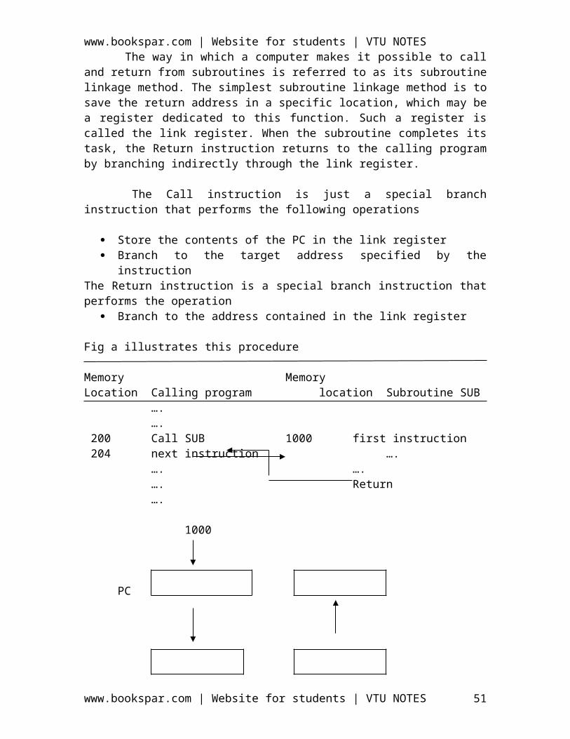
www.bookspar.com | Website for students | VTU NOTES Another feature available on many dynamic memory chips is that once the row
address is loaded, successive locations can be accessed by loading only column addresses. Such block transfers can be carried out typically at a rate that is double that for transfers involving random addresses. Such a feature is useful when memory access follow a regular pattern, for example, in a graphics terminal.
Because of their high density and low cost, dynamic memories are widely used in the main memory units of computers. Commercially available chips range in size from 1k to 4M bits or more, and are available in various organizations like 64k x 1, 16k x 4, 1MB x 1 etc.
DESIGN CONSIDERATION FOR MEMORY SYSTEMS:-
The choice of a RAM chip for a given application depends on several factors like speed, power dissipation, size of the chip, availability of block transfer feature etc.
Bipolar memories are generally used when very fast operation is the primary requirement. High power dissipation in bipolar circuits makes it difficult to realize high bit densities.
Dynamic MOS memory is the predominant technology used in the main memories of computer, because their high bit-density makes it possible to implement large memories economically.
Static MOS memory chips have higher densities and slightly longer access times compared to bipolar chips. They have lower densities than dynamic memories but are easier to use because they do not require refreshing.
Design using static Memory Chips: -
Consider the design of a memory system of 64k x 16 using 16k x 1 static memory chips. We can use a column of 4 chips to implement one bit position. Sixteen such sets provide the required 64k x 16 memories. Each chip has a control input called chip select, which should be set to 1 to enable the chip to participate in a read or write operation. When this signal is 0, the chip is electrically isolated from the rest of the system. The high-order 2 bits of the 16-bit address bus are decoded to obtain the four chip select control signals, and the remaining 14address bits are used to access specific bit locations inside each chip of the selected row. The /W input of all chips are fed together to provide a common Read/ control. This organization is shown in the following figure.
21-bit addressesA0
A1..
www.bookspar.com | Website for students | VTU NOTES 51

www.bookspar.com | Website for students | VTU NOTES
A19 A20
21-bit decoder
512 K x 8memory chip
D31-24
D23-16 D15-8 D7-0
Design using Dynamic Memory Chips: -
The design of a memory system using dynamic memory chips is similar to the design using static memory chips, but with the following important differences in the control circuitry.
The row and column parts of the address of each chip have to be multiplexed; A refresh circuit is needed; and The timing of various steps of a memory cycle must be carefully controlled.
A memory system of 256k x 16 designed using 64k x 1 DRAM chips, is shown below;
www.bookspar.com | Website for students | VTU NOTES 52

www.bookspar.com | Website for students | VTU NOTES
The memory unit is assumed to be connected to an asynchronous memory bus that has 18 address lines (ADRS 17-0), 16 data lines (DATA15-0), two handshake signals (Memory request and MFC), and a Read/ line to specify the operation (read to Write).
The memory chips are organized into 4 rows, with each row having 16 chips. Thus each column of the 16 columns implements one bit position. The higher order 12 bits of the address are decoded to get four chip select control signals which are used to select one of the four rows. The remaining 16 bits, after multiplexing, are used to access specific bit locations inside each chip of the selected row. The R/W inputs of all chips are tied together to provide a common Read/Write control. The DI and DO lines, together, provide D15 – D0 i.e. the data bus DATA15-0.
The operation of the control circuit can be described by considering a normal memory read cycle. The cycle begins when the CPU activates the address, the Read/ and the Memory Request lines. When the memory request line becomes active, the Access control block sets the start signal to 1. The timing control block responds by setting Busy lines to 1, in order to prevent the access control block from accepting new requests until the current cycle ends. The timing control block then loads the row and column addresses into the memory chips by activating the RAS and CAS lines. During this time, it uses the Row/ line to select first the row address, ADRS15-8, followed by the column address, ADRS(7-0).
Refresh Operation:-
The Refresh control block periodically generates Refresh, requests, causing the access control block to start a memory cycle in the normal way. This block allows the refresh operation by activating the Refresh Grant line. The access control block arbitrates between Memory Access requests and Refresh requests, with priority to Refresh requests in the case of a tie to ensure the integrity of the stored data.
www.bookspar.com | Website for students | VTU NOTES 53

www.bookspar.com | Website for students | VTU NOTES
As soon as the Refresh control block receives the Refresh Grant signal, it activates the Refresh line. This causes the address multiplexer to select the Refresh counter as the source and its contents are thus loaded into the row address latches of all memory chips when the RAS signal is activated. During this time the R/ line may be low, causing an inadvertent write operation. One way to prevent this is to use the Refresh line to control the decoder block to deactivate all the chip select lines. The rest of the refresh cycle is the same as in a normal cycle. At the end, the Refresh control block increments the refresh counter in preparation for the next Refresh cycle.
Even though the row address has 8 bits, the Refresh counter need only be 7 bits wide because of the cell organization inside the memory chips. In a 64k x 1 memory chip, the 256x256 cell array actually consists of two 128x256 arrays. The low order 7 bits of the row address select a row from both arrays and thus the row from both arrays is refreshed!
Ideally, the refresh operation should be transparent to the CPU. However, the response of the memory to a request from the CPU or from a DMA device may be delayed if a Refresh operation is in progress. Further, in the case of a tie, Refresh operation is given priority. Thus the normal access may be delayed. This delay will be more if all memory rows are refreshed before the memory is returned to normal use. A more common scheme, however, interleaves Refresh operations on successive rows with accesses from the memory bus. In either case, Refresh operations generally use less than 5% of the available memory cycles, so the time penalty caused by refreshing is very small.
The variability in the access times resulting from refresh can be easily accommodated in an asynchronous bus scheme. With synchronous buses, it may be necessary for the Refresh circuit to request bus cycles as a DMA device would!
Semi Conductor Rom Memories: - Semiconductor read-only memory (ROM) units are well suited as the control
store components in micro programmed processors and also as the parts of the main memory that contain fixed programs or data.
The following figure shows a possible configuration for a bipolar ROM cell.
The word line is normally held at a low voltage. If a word is to be selected, the voltage of the corresponding word line is momentarily raised, which causes all transistors whose emitters are connected to their corresponding bit lines to be turned on. The current that flows from the voltage supply to the bit line can be detected by a sense circuit. The bit positions in which current is detected are read as 1s, and the remaining bits are read as Os.
www.bookspar.com | Website for students | VTU NOTES 54

www.bookspar.com | Website for students | VTU NOTESTherefore, the contents of a given word are determined by the pattern of emitter to bit-line connections similar configurations are possible in MOS technology.
Data are written into a ROM at the time of manufacture programmable ROM (PROM) devices allow the data to be loaded by the user. Programmability is achieved by connecting a fuse between the emitter and the bit line. Thus, prior to programming, the memory contains all 1s. The user can inserts Os at the required locations by burning out the fuses at these locations using high-current pulses. This process is irreversible.
ROMs are attractive when high production volumes are involved. For smaller numbers, PROMs provide a faster and considerably less expensive approach.
Chips which allow the stored data to be erased and new data to be loaded. Such a chip is an erasable, programmable ROM, usually called an EPROM. It provides considerable flexibility during the development phase. An EPROM cell bears considerable resemblance to the dynamic memory cell. As in the case of dynamic memory, information is stored in the form of a charge on a capacitor. The main difference is that the capacitor in an EPROM cell is very well insulated. Its rate of discharge is so low that it retains the stored information for very long periods. To write information, allowing charge to be stored on the capacitor.
The contents of EPROM cells can be erased by increasing the discharge rate of the storage capacitor by several orders of magnitude. This can be accomplished by allowing ultraviolet light into the chip through a window provided for that purpose, or by the application of a high voltage similar to that used in a write operation. If ultraviolet light is used, all cells in the chip are erased at the same time. When electrical erasure is used, however, the process can be made selective. An electrically erasable EPROM, often referred to as EEPROM. However, the circuit must now include high voltage generation. Some E2PROM chips incorporate the circuitry for generating these voltages o the chip itself. Depending on the requirements, suitable device can be selected.
Classification of memory devices
Memory devise
Read/Write Read only
Static Dynamic ROM PROM Erasable PROM
Bi-polar MOS UV Erasable PROM E2PROM
Cache Memory:-
Analysis of a large number of typical programs has shown that most of their execution time is spent on a few main row lines in which a number of instructions are
www.bookspar.com | Website for students | VTU NOTES 55
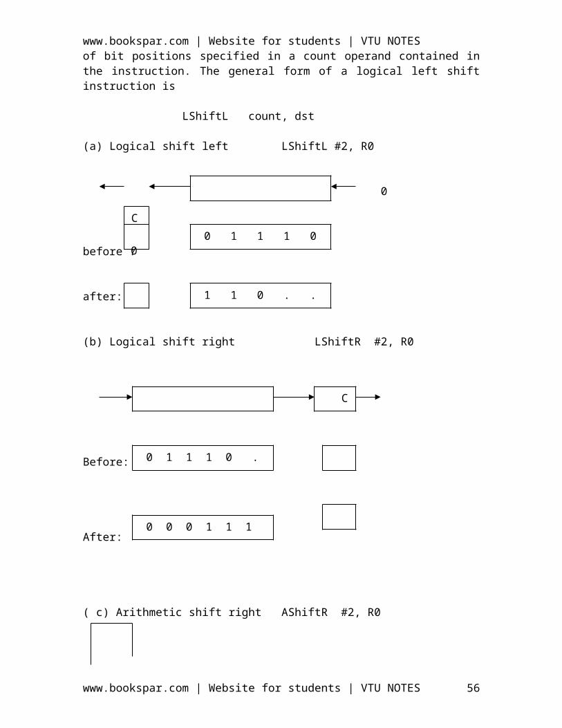
www.bookspar.com | Website for students | VTU NOTESexecuted repeatedly. These instructions may constitute a simple loop, nested loops or few procedure that repeatedly call each other. The main observation is that many instructions in a few localized are as of the program are repeatedly executed and that the remainder of the program is accessed relatively infrequently. This phenomenan is referred to as locality of reference.
If the active segments of a program can be placed in a fast memory, then the total execution time can be significantly reduced, such a memory is referred as a cache memory which is in served between the CPU and the main memory as shown in fig.1
Fig.1 cache memory between main memory & cpu.
Two Level memory Hierarchy: We will adopt the terms Primary level for the smaller, faster memory and the secondary level for larger, slower memory, we will also allow cache to be a primary level with slower semiconductor memory as the corresponding secondary level. At a different point in the hierarchy, the same S.C memory could be the primary level with disk as the secondary level.
Primary and Secondary addresses:-
A two level hierarchy and its addressing are illustrated in fig.2. A system address is applied to the memory management unit (MMU) that handles the mapping function for the particular pair in the hierarchy. If the MMU finds the address in the Primary level, it provides Primary address, which selects the item from the Primary memory. This translation must be fast, because every time memory is accessed, the system address must be translated. The translation may fail to produce a Primary address because the requested items is not found, so that information can be retrieved from the secondary level and transferred to the Primary level.
Hits and Misses:- Successful translation of reference into Primary address is called a hit, and failure is a miss. The hit ratio is (1-miss ratio). If tp is the Primary memory access time and ts is the secondary access time, the average access time for the two level hierarchy is
ta = h tp + (1-h)ts
www.bookspar.com | Website for students | VTU NOTES 56
CPU CACHE Main memory

www.bookspar.com | Website for students | VTU NOTES
The Cache:- The Mapping Function
Fig. Shows a schematic view of the cache mapping function. The mapping function is responsible for all cache operations. It is implemented in hardware, because of the required high speed operation. The mapping function determines the following.
Placement strategies – Where to place an incoming block in the cache Replacement strategies – Which block to replace when a cache miss occurs How to handle Read and Writes up as cache hit and mises
Three different types of mapping functions are in common use1. Associative mapping cache2. Direct mapping cache3. Block-set-associative mapping cache
1. Associative mapped caches:- In this any block from main memory can be placed any where in the cache. After being placed in the cache, a given block is identified uniquely by its main memory block number, referred to as the tag, which is stored inside a separate tag memory in the cache.
Regardless of the kind of cache, a given block in the cache may or may not contain valid information. For example, when the system has just been powered up add before the cache has had any blocks loaded into it, all the information there is invalid. The cache maintains a valid bit for each block to keep track of whether the information in the corresponding block is valid.
Fig4. shows the various memory structures in an associative cache, The cache itself contain 256, 8byte blocks, a 256 x 13 bit tag memory for holding the tags of the blocks currently stored in the cache, and a 256 x 1 bit memory for storing the valid bits, Main memory contains 8192, 8 byte blocks. The figure indicates that main memory address references are partition into two fields, a 3 bit word field describing the location of the desired word in the cache line, and a 13 bit tag field describing the main memory block number desired. The 3 bit word field becomes essentially a “cache address” specifying where to find the word if indeed it is in the cache.
The remaining 13 bits must be compared against every 13 bit tag in the tag memory to see if the desired word is present.
www.bookspar.com | Website for students | VTU NOTES 57
CPUWord Cache Block
MainMemory
Mapping function

www.bookspar.com | Website for students | VTU NOTES
In the fig, above, main memory block 2 has been stored in the 256 cache block and so the 256th tag entry is 2 mm block 119 has been stored in the second cache block corresponding entry in tag memory is 119 mm block 421 has been stored in cache block 0 and tag memory location 0 has been set to 421. Three valid bits have also been set, indicating valid information in these locations.
The associative cache makes the most flexible and complete use of its capacity, storing blocks wherever it needs to, but there is a penalty to be paid for this flexibility the tag memory must be searched in for each memory reference.
Fig.5 shows the mechanism of operation of the associative cache. The process begins with the main memory address being placed in the argument register of the (associative) tag memory (1) if there is a match (hit), (2) and if the ratio bit for the block is set (3), then the block is gated out of the cache (4), and the 3 bit offset field is used to select the byte corresponding to the block offset field of the main memory address (5) That byte is forwarded to the CPU, (6)
2. Direct mapped caches:- In this a given main memory block can be placed in one and only one place in the cache. Fig6. Shows an example of a direct – mapped cache. For simplicity, the example again uses a 256 block x 8 byte cache and a 16 bit main memory
www.bookspar.com | Website for students | VTU NOTES 58

www.bookspar.com | Website for students | VTU NOTESaddress. The main memory in the fig. has 256 rows x 32 columns, still fielding 256 x 32 = 8192 = 213 total blocks as before. Notice that the main memory address is partitioned into 3 fields. The word field still specifies the word in the block. The group field specifies which of the 256 cache locations the block will be in, if it is indeed in the cache. The tag field specifies which of the 32 blocks from main memory is actually present in the cache. Now the cache address is composed of the group field, which specifies the address of the block location in the cache and the word field, which specifies the address of the word in the block. There is also valid bit specifying whether the information in the selected block in valid.
The fig.6 shows block 7680, from group 0 of MM placed in block location 0 of the cache and the corresponding tag set to 30. Similarly MM block 259 is in MM group 2, column 1, it is placed in block location 2 of the cache and the corresponding tag memory entry is 1.
The tasks required of the direct – mapped cache in servicing a memory request are shown in fig7.
The fig. shows the group field of the memory address being decoded 1) and used to select the tag of the one cache block location in which the block must be stored if it is the cache. If the valid bit for that block location is gated (2), then that tag is gated out, (3) and compared with the tag of the incoming memory address (4), A cache hit gates the cache block out (5) and the word field selects the specified word from the block (6), only one tag needs to be compared, resulting in considerably less hardware than in the associative memory case.
www.bookspar.com | Website for students | VTU NOTES 59

www.bookspar.com | Website for students | VTU NOTES
The direct mapped cache has the advantage of simplicity, but the obvious disadvantage that only a single block from a given group can be present in the cache at any given time.
3. Block-set-Associative cache:-
Block-set-Associative caches share properties of both of the previous mapping functions. It is similar to the direct-mapped cache, but now more than one block from a given group in main memory can occupy the same group in the cache. Assume the same main memory and block structure as before, but with the cache being twice as large, so that a set of two main memory blocks from the same group can occupy a given cache group.
Fig 8 shows a 2 way set associative cache that is similar to the direct mapped cache in the previous example, but with twice as many blocks in the cache, arranged so that a set of any two blocks from each main memory group can be stored in the cache. MM is still partitioned into an 8 bit set field and a 5 bit tag field, but now there are two possible places in which a given block can reside and both must be searched associatively.
The cache group address is the same as that of the direct matched cache, an 8 bit block location and a 3 bit word location. Fig 8 shows that the cache entries corresponding to the second group contains blocks 513 and 2304. the group field now called the set field, is again decoded and directs the search to the correct group and new only the tags in the selected group must be searched. So instead of 256 compares, the cache only needs to do 2.
For simplicity, the valid bits are not shown, but they must be present. The cache hard ware would be similar so that shown in fig 7. but there would be two simultaneous comparisons of the two blocks in the set.
www.bookspar.com | Website for students | VTU NOTES 60

www.bookspar.com | Website for students | VTU NOTES
Solved Problems:-1. A block set associative cache consists of a total of 64 blocks divided into 4 block
sets. The MM contains 4096 blocks each containing 128 words.a) How many bits are there in MM address?b) How many bits are there in each of the TAG, SET & word fields
Solution:- Number of sets = 64/4 = 16Set bits = 4(24 = 16)Number of words = 128Word bits = 7 bits (27 = 128)MM capacity : 4096 x 128 (212 x 27 = 219)
a) Number of bits in memory address = 19 bitsb)
8 4 7TAG SET WORDTAG bits = 19 – (7+4) = 8 bits.
2. A computer system has a MM capacity of a total of 1M 16 bits words. It also has a 4K words cache organized in the block set associative manner, with 4 blocks per set & 64 words per block. Calculate the number of bits in each of the TAG, SET & WORD fields of MM address format.
Solution: Capacity: 1M (220 = 1M)Number of words per block = 64Number of blocks in cache = 4k/64 = 64
Number of sets = 64/4 = 16Set bits = 4 (24 = 16)Word bits = 6 bits (26 = 64)Tag bits = 20-(6+4) = 10 bitsMM address format
10 4 6 TAG SET WORD
www.bookspar.com | Website for students | VTU NOTES 61

www.bookspar.com | Website for students | VTU NOTES
Virtual Memory:-
Virtual memory is the technique of using secondary storage such as disks to enter the apparent size of accessible memory beyond its actual physical size. Virtual memory is implemented by employing a memory-management unit (MMU) to translate every logical address reference into a physical address reference as shown in fig 1. The MMU is imposed between the CPU and the physical memory where it performs these translations under the control of the operating system. Each memory reference is sued by the CPU is translated from the logical address space to the physical address space. Mapping tables guide the translation, again under the control of the operating system.
Physical Address Logical address
Virtual memory usually demand paging, which means that a Page is moved from disk into main memory only when the processor accesses a word on that page. Virtual memory pages always have a place on the disk once they are created, but are copied to main memory only on a miss or page fault.
Advantages of Virtual memory:-1. Simplified addressing:- Each program unit can be compiled into its own
memory space, beginning at address O and extending far beyond the limits of physical memory. Programs and data structures do not require address relocation at load time, nor must they be broken into fragments merely to accommodate memory limitations.
2. Cost effective use of memory: - Less expensive disk storage can replace more expensive RAM memory, since the entire program does not need to occupy physical memory at one time.
www.bookspar.com | Website for students | VTU NOTES 62
CPU MMU
Virtual address
Cache Main Memory-
---
Mapping tastes Disk

www.bookspar.com | Website for students | VTU NOTES3. Access control: - Since each memory reference must be translated, it can be
simultaneously checked for read, write and execute privileges. This allows hardward level control of access to system resources and also prevents and also prevents buggy programs or intruders from causing damage to the resources of other users or the system.
a) Memory management by segmentation:- Segmentation allows memory to be divided into segments of varying sizes depending upon requirements. Fig 2. Shows a main memory containing five segments identified by segment numbers. Each segment beings at a virtual address 0, regardless of where it is located in physical memory.
Each virtual address arriving from the CPU is added to the contents of the segment base register in the MMU to form the physical address. The virtual address may also optionally be compared to a segment limit register to trap reference beyond a specified limit.
b) Memory management by paging:- Fig 3 shows a simplified mechanism for virtual address translation in a paged MMU. The process begins in a manner similar to the segmentation process. The virtual address composed of a high order page number and a low order word number is applied to MMU. The virtual page number is limit checked to be certain that the page is within the page table, and if it is, it is added to the page table base to yield the page table entry. The page table entry contains several control fields in addition to the page field. The control fields may include access control bits, a presence bit, a dirty bit and one or more use bits, typically the access control field will include bits specifying read, write and perhaps execute permission. The presence bit indicates whether the page is currently in main memory. The use bit is set upon a read or write to the specified page, as an indication to the replaced algorithm in case a page must be replaced.
www.bookspar.com | Website for students | VTU NOTES 63

www.bookspar.com | Website for students | VTU NOTES
If the presence bit indicates a hit, then the page field of the page table entry will contain the physical page number. If the presence bit is a miss, which is page fault, then the page field of the page table entry which contains an address is secondary memory where the page is stored. This miss condition also generates an interrupt. The interrupt service routine will initiate the page fetch from secondary memory and with also suspended the requesting process until the page has been bought into main memory. If the CPU operation is a write hit, then the dirty bit is set. If the CPU operation is a write miss, then the MMU with begin a write allocate process.
Problems:-1. An address space is specified by 24 bits & the corresponding memory space is 16
bits.a) How many words are there in address space?b) How many words are there in memory space?c) If a page has 2k words, how many pages & blocks are in the system?
Solution:-a) Address space = 24 bits224 = 24.220 = 16M wordsb) Memory space: 16 bits216 = 64k wordsc) page consists of 2k wordsNumber of pages in add space = 16M/2K = 8000Number of blocks = 64k/2k = 32 blocks
2. A virtual memory has a page size of 1k words. There are 8 pages & 4 blocks. The associative memory page table has the following entries.
Page block Make a list of virtual addresses (in decimal ) that will cause a page 0 3 by cpu fault of used
www.bookspar.com | Website for students | VTU NOTES 64

www.bookspar.com | Website for students | VTU NOTES
1 1
4 2
6 0
The page numbers 2, 3, 5 & 7 are not available in associative memory page table & hence cause a page fault.
Peripheral Devices:1. Magnetic Disk Drives: Hard disk Drive organization:
The modern hard disk drive is a system in itself. It contains not only the disks that are used as the storage medium and the read write heads that access the raw data encoded on them, but also the signal conditioning circuitry and the interface electronics that separate the system user from the details & getting bits on and off the magnetic surface. The drive has 4 platters with read/write heads on the top and bottom of each platter. The drive rotates at a constant 3600rpm.
Platters and Read/Write Heads: - The heart of the disk drive is the stack of rotating platters that contain the encoded data, and the read and write heads that access that data. The drive contains five or more platters. There are read/write heads on the top and bottom of each platter, so information can be recorded on both surfaces. All heads move together across the platters. The platters rotate at constant speed usually 3600 rpm.
Drive Electronics: - The disk drive electronics are located on a printed circuit board attached to the disk drive. After a read request, the electronics must seek out and find the block requested, stream is off of the surface, error check and correct it, assembly into bytes, store it in an on-board buffer and signal the processor that the task is complete.
To assist in the task, the drive electronics include a disk controller, a special purpose processor.
Data organization on the Disk:- The drive needs to know where the data to be accessed is located on the disk. In order to provide that location information, data is organized on the disk platters by tracks and sectors. Fig 13 shows simplified view of the organization of tracks and sectors on a disk. The fig. Shows a disk with 1024 tracks, each of which has 64 sectors. The head can determine which track it is on by counting tracks from a known location and sector identities are encoded in a header written on the disk at the front of each sector.
www.bookspar.com | Website for students | VTU NOTES 65

www.bookspar.com | Website for students | VTU NOTES The number of bytes per sector is fixed for a given disk drive, varying in size
from 512 bytes to 2KB. All tracks with the same number, but as different surfaces, form a cylinder.
The information is recorded on the disk surface 1 bit at a time by magnetizing a small area on the track with the write head. That bit is detected by sending the direction of that magnetization as the magnetized area passes under the read head as shown in fig 14.
Fig 5. shows how a typical sector might be organized. The header usually contains both synchronization and location information. The synchronization information allows the head positioning circuitry to keep the heads centered on the track and the location information allows the disk controller to determine the sectors & identifies as the header passes, so that the data can be captured if it is read or stored, if it is a write. The 12 bytes of ECC (Error Correcting Code) information are used to detect and correct errors in the 512 byte data field.
Generally the disk drive manufacturer initializes or formats the drive by writing its original track and sector information on the surfaces and checks to determine whether data can be written and read from each sector. If any sectors are found to be bad, that is incapable of being used even with ECC, then they are marked as being defective so their use can be avoided by operating system.
The operating system interface:- The operating system specifies the track, sector and surface of the desired block. The disk controller translates that requests to a series of low level disk operations. Fig 15 shows logical block address (LBA) used to communicate requests to the drive controller.
Head #, Cylinder #, and Sector # refer to the starting address of the information and sector count specifies the number of sectors requested.
4 4 16 8 8Drive # Head # Cylinder # Sector # Sector count
www.bookspar.com | Website for students | VTU NOTES 66

www.bookspar.com | Website for students | VTU NOTESLogical block address
Fig 15. Block address for disk address.
The Disk Access Process:- Let us follow the process of reading a sector from the disk1. The OS communicates the LBA to the disk drive and issues the read command.2. The drive seeks the correct track by moving the heads to the correct position and
enabling the one on the specified surface. The read feed reads sector numbers as they travel by until the requested one is found.
3. Sector data and ECC stream into a buffer on the drive interface. ECC is done as the fly.
4. The drive communicates ‘data ready’ to the OS.5. The OS reads data, either byte by byte or by issuing a DMA command.
Disk Drive Dynamic Properties: -
Dynamic properties are those that deal with the access time for the reading and writing of data. The calculation of data access time is not simple. It depends not only as the rotational speed of the disk, but also the location of the read/write head when it begins the access. There are several measures of data access times.
1. Seek time: - Is the average time required to move the read/write head to the desired track. Actual seek time which depend on where the head is when the request is received and how far it has to travel, but since there is no way to know what these values will be when an access request is made, the average figure is used. Average seek time must be determined by measurement. It will depend on the physical size of the drive components and how fast the heads can be accelerated and decelerated. Seek times are generally in the range of 8-20 m sec and have not changed much in recent years.
2. Track to track access time: - Is the time required to move the head from one track to adjoining one. This time is in the range of 1-2 m sec.
3. Rotational latency: - Is the average time required for the needed sector to pass under head once and head has been positioned once at the correct track. Since on the average the desired sector will be half way around the track from where the head is when the head first arrives at the track, rotational latency is taken to be ½ the rotation time. Current rotation speeds are from 3600 to 7200 rpm, which yield rotational latencies in the 4-8 ms range.
4. Average Access time:- Is equal to seek time plus rotational latency.5. Burst rate: - Is the maximum rate at which the drive produces or accepts data
once the head reaches the desired sector, It is equal to the rate at which data bits stream by the head, provided that the rest of the system can produce or accept data at that rate
Burst rate (byte/sec) = rows/sec * sector/row * bytes/sector6. Sustained data rate: - Is the rate at which data can be accessed over a sustained
period of time.
www.bookspar.com | Website for students | VTU NOTES 67

www.bookspar.com | Website for students | VTU NOTESProblems 1: A hard drive has 8 surface, with 521 tracks per surface and a constant 64 sectors per track. Sector size is 1KB. The average seek time is 8 m sec, the track to track access time is 1.5 m sec and the drive runs at 3600 rpm. Successive tracks in a cylinder can be read without head movement.
a) What is the drive capacity?b) What is the average access time for the drive?c) Estimate the time required to transfer a 5MB file?d) What is the burst transfer rate?
Solution:-a) Capacity = Surfaces x tracks x sectors x sector size
= 8 x 521 x 64 x 1k = 266.752MBb) Rotational latency : Rotation time/2 = 60/3600x2 = 8.3 m sec
Average Access time = Seek time + Rotational latency= 8 m sec + 8.3 m sec = 16.3 m sec
c) Assume the file is stored in successive sectors and tracks starting at sector #0, track#0 of cylinder #i. A 5MB file will need 1000 blocks and occupy from cylinder #1, track #0, sector #0 to cylinder #(i+9), track #6, sector #7, we also assume the size of disk buffer is unlimited.
The disk needs 8ms, which is the seek time, to find the cylinder #i, 8.3 ms to find sector #0 and 8 x (60/3600) seconds to read all 8 tracks data of this cylinder. Then the time needed for the read to move to next adjoining track will be only 1.5 m sec.
Which is the track to track access time. Assume a rotational latency before each new track.
Access time = 8+9(8.38x16.6+1.5)+8.3+6x16.6+8/64x16.6 = 1406.6 m sec
d) Burst rate = rows/sec x sectors/row x bytes/sector= 3600/60 x 64 x 1k = 3.84 MB/sec
Problem 2: A floppy disk drive has a maximum area bits density of 500 bits per mm 2. its innermost track is at a radius of 2cm, and its outermost track is at radius of 5cm. It rotates at 300rpm.
a) What is the total capacity of the drive?b) What is its burst data rate in bytes per second?
Solution:-
a) At the maximum area density the bit spacing equals the track spacing t, so 500 = 1/t2
or t = 0.045 mm
www.bookspar.com | Website for students | VTU NOTES 68

www.bookspar.com | Website for students | VTU NOTESThe number of tracks = (50-20)/0.045 = 666
The number of bits per track = 40p/0.045 2791Thus the unformatted or raw capacity is 666 x 2791 = 1,841,400 bits
b) Given 5 raw per second the (raw)burst rate isRev/second x bytes/rev = 5 x 2791/8 = 1744 bytes/sec
Optical DisksCompact Disk (CD) Technology:- The optical technology that is used for CD system is based on laser light source. A laser beam is directed onto the surface of the spinning disk. Physical indentations in the surface are arranged along the tracks of the disk. They reflect the focused beam towards a photo detector, which detects the stored binary patterns.
The laser emits a coherent light beam that is sharply focused on the surface of the disk. Coherent light consists of Synchronized waves that have the same wavelength. If a coherent light beam is combined with another beam of the same kind, and the two beams are in phase, then the result will be brighter beam. But, if a photo detector is used to detect the beams, it will detect a bright spot in the first case and a dark spot in the second case.
A cross section of a small portion of a CD shown in fig. 16
The bottom payer is Polycarbonate plastic, which functions as a clear glass base. The surface of this plastic is Programmed to store data by indenting it with pits. The unindented parts are called lands. A thin layer of reflecting aluminium material is placed on top of a programmed disk. The aluminium is then covered by a protective acrylic. Finally the topmost layer is deposited and stamped with a label.
The laser source and the Photo detector are positioned below the polycarbonate plastic. The emitted bean travels through this plastic, reflects off the aluminium layer and travels back toward photo detector.
Some important optical disks are listed below1. CD-ROM2. CD-RWs (CD-re writables)3. DVD technology (Digital Versatile disk)
Problem 1:- A certain two-way associative cache has an access time of 40 nano seconds, compared to a miss time of 90 nano seconds. Without the cache, main memory access time was 90 nano seconds. Without the cache, main memory access time was 70 nano seconds. Running a set of benchmarks with and without the cache indicated a speed up of 1.4.
www.bookspar.com | Website for students | VTU NOTES 69

www.bookspar.com | Website for students | VTU NOTESWhat is the approximate hit rate?Solution:- Hit:tn = 40 nano seconds
Miss:tm = 90No Cache: tn = 70
Access time with Cache ta = h.tn+(1-h)tm = tn-h(tn-tn)Speed up S = tn/ta = 70/90-50h = 1.4Which gives hit ratio h = 80%
Problem 2: A 16 MB main memory has a 32 KB direct mapped Cache with 8 bytes per line.
a. How many lines are there in the Cache.b. Show how the main memory address is Partitioned?
Solution:- a. Number of Cache lines = 215/23 = 212 lines b. 23 15 14 32 0
Tag (9 bits) Group (12 bits) Bytes (3)16MB = 24.220 = 224
Problems 3:- A certain memory system has a 32 MB main memory and a 64 KB Cache. Block are 16 bytes in sizes. Show the field in memory address if the cache is
a. Associativeb. Direct mappedc. 8 way set-associative
Solution:- A 32 MB memory requires a 25 bit address. A byte in the 64 KB Cache is located by a 16 bit address. 4 bits select one byte from a 16 byte block.
a. For an associative Cache, a main memory address appear as
Tag Byte
b. For direct mapped Cache, a main memory address appears as
Tag Group Byte
c. For an 8-way set-associative Cache, a main memory address appears as
Tag Group Byte
www.bookspar.com | Website for students | VTU NOTES 70
24 4 3 0
24 16 15 4 3 0
24 13 12 4 3 0

www.bookspar.com | Website for students | VTU NOTESChapter – 03
ACCESSING I/O DEVICES: - A simple arrangement to connect I/O devices to a computer is to use a single bus
arrangement. The bus enables all the devices connected to it to exchange information. Typically, it consists of three sets of lines used to carry address, data, and control signals. Each I/O device is assigned a unique set of addresses. When the processor places a particular address on the address line, the device that recognizes this address responds to the commands issued on the control lines. The processor requests either a read or a write operation, and the requested data are transferred over the data lines, when I/O devices and the memory share the same address space, the arrangement is called memory-mapped I/O.
With memory-mapped I/O, any machine instruction that can access memory can be used to transfer data to or from an I/O device. For example, if DATAIN is the address of the input buffer associated with the keyboard, the instruction
Move DATAIN, R0
Reads the data from DATAIN and stores them into processor register R0. Similarly, the instruction
Move R0, DATAOUT
Sends the contents of register R0 to location DATAOUT, which may be the output data buffer of a display unit or a printer.
Most computer systems use memory-mapped I/O. some processors have special In and Out instructions to perform I/O transfers. When building a computer system based on these processors, the designer had the option of connecting I/O devices to use the special I/O address space or simply incorporating them as part of the memory address space. The I/O devices examine the low-order bits of the address bus to determine whether they should respond.
The hardware required to connect an I/O device to the bus. The address decoder enables the device to recognize its address when this address appears on the address lines. The data register holds the data being transferred to or from the processor. The status register contains information relevant to the operation of the I/O device. Both the data and status registers are connected to the data bus and assigned unique addresses. The address decoder, the data and status registers, and the control circuitry required to coordinate I/O transfers constitute the device’s interface circuit.
I/O devices operate at speeds that are vastly different from that of the processor. When a human operator is entering characters at a keyboard, the processor is capable of executing millions of instructions between successive character entries. An instruction that reads a character from the keyboard should be executed only when a character is available in the input buffer of the keyboard interface. Also, we must make sure that an input character is read only once.
www.bookspar.com | Website for students | VTU NOTES 71

www.bookspar.com | Website for students | VTU NOTES
This example illustrates program-controlled I/O, in which the processor repeatedly checks a status flag to achieve the required synchronization between the processor and an input or output device. We say that the processor polls the device. There are two other commonly used mechanisms for implementing I/O operations: interrupts and direct memory access. In the case of interrupts, synchronization is achieved by having the I/O device send a special signal over the bus whenever it is ready for a data transfer operation. Direct memory access is a technique used for high-speed I/O devices. It involves having the device interface transfer data directly to or from the memory, without continuous involvement by the processor.
The routine executed in response to an interrupt request is called the interrupt-service routine, which is the PRINT routine in our example. Interrupts bear considerable resemblance to subroutine calls. Assume that an interrupt request arrives during execution of instruction i in figure 1
Program 1 Program 2COMPUTER routine PRINT routine
1
2 ....
Interrupt iOccurs i+1here
…M
Figure 1. Transfer of control through the use of interrupts
The processor first completes execution of instruction i. Then, it loads the program counter with the address of the first instruction of the interrupt-service routine. For the time being, let us assume that this address is hardwired in the processor. After execution of the interrupt-service routine, the processor has to come back to instruction i +1. Therefore, when an interrupt occurs, the current contents of the PC, which point to instruction i+1, must be put in temporary storage in a known location. A Return-from-interrupt instruction at the end of the interrupt-service routine reloads the PC from the temporary storage location, causing execution to resume at instruction i +1. In many processors, the return address is saved on the processor stack.
We should note that as part of handling interrupts, the processor must inform the
device that its request has been recognized so that it may remove its interrupt-request signal. This may be accomplished by means of a special control signal on the bus. An interrupt-acknowledge signal. The execution of an instruction in the interrupt-service
www.bookspar.com | Website for students | VTU NOTES 72

www.bookspar.com | Website for students | VTU NOTESroutine that accesses a status or data register in the device interface implicitly informs that device that its interrupt request has been recognized.
So far, treatment of an interrupt-service routine is very similar to that of a subroutine. An important departure from this similarity should be noted. A subroutine performs a function required by the program from which it is called. However, the interrupt-service routine may not have anything in common with the program being executed at the time the interrupt request is received. In fact, the two programs often belong to different users. Therefore, before starting execution of the interrupt-service routine, any information that may be altered during the execution of that routine must be saved. This information must be restored before execution of the interrupt program is resumed. In this way, the original program can continue execution without being affected in any way by the interruption, except for the time delay. The information that needs to be saved and restored typically includes the condition code flags and the contents of any registers used by both the interrupted program and the interrupt-service routine.
The task of saving and restoring information can be done automatically by the processor or by program instructions. Most modern processors save only the minimum amount of information needed to maintain the registers involves memory transfers that increase the total execution time, and hence represent execution overhead. Saving registers also increase the delay between the time an interrupt request is received and the start of execution of the interrupt-service routine. This delay is called interrupt latency.
In some earlier processors, particularly those with a small number of registers, all registers are saved automatically by the processor hardware at the time an interrupt request is accepted. The data saved are restored to their respective registers as part of the execution of the Return-from interrupt instruction. Some computers provide two types of interrupts. One saves all register contents, and the other does not. A particular I/O device may use either type, depending upon its response-time requirements. Another interesting approach is to provide duplicate sets of processor registers. In this case, a different set of registers can be used by the interrupt-service routine, thus eliminating the need to save and restore registers.
INTERRUPT HARDWARE:-
We pointed out that an I/O device requests an interrupt by activating a bus line called interrupt-request. Most computers are likely to have several I/O devices that can request an interrupt. A single interrupt-request line may be used to serve n devices as depicted. All devices are connected to the line via switches to ground. To request an interrupt, a device closes its associated switch. Thus, if all interrupt-request signals INTR1 to INTRn are inactive, that is, if all switches are open, the voltage on the interrupt-request line will be equal to Vdd. This is the inactive state of the line. Since the closing of one or more switches will cause the line voltage to drop to 0, the value of INTR is the logical OR of the requests from individual devices, that is,
INTR = INTR1 + ………+INTRn
www.bookspar.com | Website for students | VTU NOTES 73

www.bookspar.com | Website for students | VTU NOTESIt is customary to use the complemented form, , to name the interrupt-request signal on the common line, because this signal is active when in the low-voltage state.
ENABLING AND DISABLING INTERRUPTS:-
The facilities provided in a computer must give the programmer complete control over the events that take place during program execution. The arrival of an interrupt request from an external device causes the processor to suspend the execution of one program and start the execution of another. Because interrupts can arrive at any time, they may alter the sequence of events from the envisaged by the programmer. Hence, the interruption of program execution must be carefully controlled.
Let us consider in detail the specific case of a single interrupt request from one device. When a device activates the interrupt-request signal, it keeps this signal activated until it learns that the processor has accepted its request. This means that the interrupt-request signal will be active during execution of the interrupt-service routine, perhaps until an instruction is reached that accesses the device in question.
The first possibility is to have the processor hardware ignore the interrupt-request line until the execution of the first instruction of the interrupt-service routine has been completed. Then, by using an Interrupt-disable instruction as the first instruction in the interrupt-service routine, the programmer can ensure that no further interruptions will occur until an Interrupt-enable instruction is executed. Typically, the Interrupt-enable instruction will be the last instruction in the interrupt-service routine before the Return-from-interrupt instruction. The processor must guarantee that execution of the Return-from-interrupt instruction is completed before further interruption can occur.
The second option, which is suitable for a simple processor with only one interrupt-request line, is to have the processor automatically disable interrupts before starting the execution of the interrupt-service routine. After saving the contents of the PC and the processor status register (PS) on the stack, the processor performs the equivalent of executing an Interrupt-disable instruction. It is often the case that one bit in the PS register, called Interrupt-enable, indicates whether interrupts are enabled.
In the third option, the processor has a special interrupt-request line for which the interrupt-handling circuit responds only to the leading edge of the signal. Such a line is said to be edge-triggered.
Before proceeding to study more complex aspects of interrupts, let us summarize the sequence of events involved in handling an interrupt request from a single device. Assuming that interrupts are enabled, the following is a typical scenario.
1. The device raises an interrupt request.2. The processor interrupts the program currently being executed.3. Interrupts are disabled by changing the control bits in the PS (except in the case of
edge-triggered interrupts).4. The device is informed that its request has been recognized, and in response, it
deactivates the interrupt-request signal.5. The action requested by the interrupt is performed by the interrupt-service routine.
www.bookspar.com | Website for students | VTU NOTES 74

www.bookspar.com | Website for students | VTU NOTES6. Interrupts are enabled and execution of the interrupted program is resumed.
HANDLING MULTIPLE DEVICES:-
Let us now consider the situation where a number of devices capable of initiating interrupts are connected to the processor. Because these devices are operationally independent, there is no definite order in which they will generate interrupts. For example, device X may request in interrupt while an interrupt caused by device Y is being serviced, or several devices may request interrupts at exactly the same time. This gives rise to a number of questions
1. How can the processor recognize the device requesting an interrupts?2. Given that different devices are likely to require different interrupt-service
routines, how can the processor obtain the starting address of the appropriate routine in each case?
3. Should a device be allowed to interrupt the processor while another interrupt is being serviced?
4. How should two or more simultaneous interrupt requests be handled?
The means by which these problems are resolved vary from one computer to another, And the approach taken is an important consideration in determining the computer’s suitability for a given application.
When a request is received over the common interrupt-request line, additional information is needed to identify the particular device that activated the line.
The information needed to determine whether a device is requesting an interrupt is available in its status register. When a device raises an interrupt request, it sets to 1 one of the bits in its status register, which we will call the IRQ bit. For example, bits KIRQ and DIRQ are the interrupt request bits for the keyboard and the display, respectively. The simplest way to identify the interrupting device is to have the interrupt-service routine poll all the I/O devices connected to the bus. The first device encountered with its IRQ bit set is the device that should be serviced. An appropriate subroutine is called to provide the requested service.
The polling scheme is easy to implement. Its main disadvantage is the time spent interrogating the IRQ bits of all the devices that may not be requesting any service. An alternative approach is to use vectored interrupts, which we describe next.
Vectored Interrupts:-
To reduce the time involved in the polling process, a device requesting an interrupt may identify itself directly to the processor. Then, the processor can immediately start executing the corresponding interrupt-service routine. The term vectored interrupts refers to all interrupt-handling schemes based on this approach.
A device requesting an interrupt can identify itself by sending a special code to the processor over the bus. This enables the processor to identify individual devices even
www.bookspar.com | Website for students | VTU NOTES 75

www.bookspar.com | Website for students | VTU NOTESif they share a single interrupt-request line. The code supplied by the device may represent the starting address of the interrupt-service routine for that device. The code length is typically in the range of 4 to 8 bits. The remainder of the address is supplied by the processor based on the area in its memory where the addresses for interrupt-service routines are located.
This arrangement implies that the interrupt-service routine for a given device must always start at the same location. The programmer can gain some flexibility by storing in this location an instruction that causes a branch to the appropriate routine.
Interrupt Nesting: -
Interrupts should be disabled during the execution of an interrupt-service routine, to ensure that a request from one device will not cause more than one interruption. The same arrangement is often used when several devices are involved, in which case execution of a given interrupt-service routine, once started, always continues to completion before the processor accepts an interrupt request from a second device. Interrupt-service routines are typically short, and the delay they may cause is acceptable for most simple devices.
For some devices, however, a long delay in responding to an interrupt request may lead to erroneous operation. Consider, for example, a computer that keeps track of the time of day using a real-time clock. This is a device that sends interrupt requests to the processor at regular intervals. For each of these requests, the processor executes a short interrupt-service routine to increment a set of counters in the memory that keep track of time in seconds, minutes, and so on. Proper operation requires that the delay in responding to an interrupt request from the real-time clock be small in comparison with the interval between two successive requests. To ensure that this requirement is satisfied in the presence of other interrupting devices, it may be necessary to accept an interrupt request from the clock during the execution of an interrupt-service routine for another device.
This example suggests that I/O devices should be organized in a priority structure. An interrupt request from a high-priority device should be accepted while the processor is servicing another request from a lower-priority device.
A multiple-level priority organization means that during execution of an interrupt-service routine, interrupt requests will be accepted from some devices but not from others, depending upon the device’s priority. To implement this scheme, we can assign a priority level to the processor that can be changed under program control. The priority level of the processor is the priority of the program that is currently being executed. The processor accepts interrupts only from devices that have priorities higher than its own.
The processor’s priority is usually encoded in a few bits of the processor status word. It can be changed by program instructions that write into the PS. These are privileged instructions, which can be executed only while the processor is running in the supervisor mode. The processor is in the supervisor mode only when executing operating
www.bookspar.com | Website for students | VTU NOTES 76

www.bookspar.com | Website for students | VTU NOTESsystem routines. It switches to the user mode before beginning to execute application programs. Thus, a user program cannot accidentally, or intentionally, change the priority of the processor and disrupt the system’s operation. An attempt to execute a privileged instruction while in the user mode leads to a special type of interrupt called a privileged instruction.
A multiple-priority scheme can be implemented easily by using separate interrupt-request and interrupt-acknowledge lines for each device, as shown in figure. Each of the interrupt-request lines is assigned a different priority level. Interrupt requests received over these lines are sent to a priority arbitration circuit in the processor. A request is accepted only if it has a higher priority level than that currently assigned to the processor.
p 1
INTA 1 INTA p
Priority arbitration Circuit
Figure2: Implementation of interrupt priority using individual interrupt-request and acknowledge lines.
Simultaneous Requests:-
Let us now consider the problem of simultaneous arrivals of interrupt requests from two or more devices. The processor must have some means of deciding which requests to service first. Using a priority scheme such as that of figure, the solution is straightforward. The processor simply accepts the requests having the highest priority.
Polling the status registers of the I/O devices is the simplest such mechanism. In this case, priority is determined by the order in which the devices are polled. When vectored interrupts are used, we must ensure that only one device is selected to send its interrupt vector code. A widely used scheme is to connect the devices to form a daisy chain, as shown in figure 3a. The interrupt-request line is common to all devices. The interrupt-acknowledge line, INTA, is connected in a daisy-chain fashion, such that the INTA signal propagates serially through the devices.
www.bookspar.com | Website for students | VTU NOTES 77
Pro
cess
or
Device 1 Device 2 Device p

www.bookspar.com | Website for students | VTU NOTES
INTA
(3.a) Daisy chain
1
INTA1
p
INTA p
Priority arbitrationCircuit (3.b) Arrangement of priority groups
When several devices raise an interrupt request and the line is activated, the processor responds by setting the INTA line to 1. This signal is received by device 1. Device 1 passes the signal on to device 2 only if it does not require any service. If device 1 has a pending request for interrupt, it blocks the INTA signal and proceeds to put its identifying code on the data lines. Therefore, in the daisy-chain arrangement, the device that is electrically closest to the processor has the highest priority. The second device along the chain has second highest priority, and so on.
The scheme in figure 3.a requires considerably fewer wires than the individual connections in figure 2. The main advantage of the scheme in figure 2 is that it allows the processor to accept interrupt requests from some devices but not from others, depending upon their priorities. The two schemes may be combined to produce the more general structure in figure 3b. Devices are organized in groups, and each group is connected at a different priority level. Within a group, devices are connected in a daisy chain. This organization is used in many computer systems.
Controlling Device Requests: -
Until now, we have assumed that an I/O device interface generates an interrupt request whenever it is ready for an I/O transfer, for example whenever the SIN flag is 1.
www.bookspar.com | Website for students | VTU NOTES 78
Pro
cess
or Device 1 Device 2 Device n
Pro
cess
or
Device Device
Device Device

www.bookspar.com | Website for students | VTU NOTESIt is important to ensure that interrupt requests are generated only by those I/O devices that are being used by a given program. Idle devices must not be allowed to generate interrupt requests, even though they may be ready to participate in I/O transfer operations. Hence, we need a mechanism in the interface circuits of individual devices to control whether a device is allowed to generate an interrupt request.
The control needed is usually provided in the form of an interrupt-enable bit in the device’s interface circuit. The keyboard interrupt-enable, KEN, and display interrupt-enable, DEN, flags in register CONTROL perform this function. If either of these flags is set, the interface circuit generates an interrupt request whenever the corresponding status flag in register STATUS is set. At the same time, the interface circuit sets bit KIRQ or DIRQ to indicate that the keyboard or display unit, respectively, is requesting an interrupt. If an interrupt-enable bit is equal to 0, the interface circuit will not generate an interrupt request, regardless of the state of the status flag.
To summarize, there are two independent mechanisms for controlling interrupt requests. At the device end, an interrupt-enable bit in a control register determines whether the device is allowed to generate an interrupt request. At the processor end, either an interrupt enable bit in the PS register or a priority structure determines whether a given interrupt request will be accepted.
Exceptions:-
An interrupt is an event that causes the execution of one program to be suspended and the execution of another program to begin. So far, we have dealt only with interrupts caused by requests received during I/O data transfers. However, the interrupt mechanism is used in a number of other situations.
The term exception is often used to refer to any event that causes an interruption. Hence, I/O interrupts are one example of an exception. We now describe a few other kinds of exceptions.
Recovery from Errors:-
Computers use a variety of techniques to ensure that all hardware components are operating properly. For example, many computers include an error-checking code in the main memory, which allows detection of errors in the stored data. If errors occur, the control hardware detects it and informs the processor by raising an interrupt.
The processor may also interrupt a program if it detects an error or an unusual condition while executing the instructions of this program. For example, the OP-code field of an instruction may not correspond to any legal instruction, or an arithmetic instruction may attempt a division by zero.
When exception processing is initiated as a result of such errors, the processor proceeds in exactly the same manner as in the case of an I/O interrupt request. It suspends the program being executed and starts an exception-service routine. This routine takes appropriate action to recover from the error, if possible, or to inform the user about it.
www.bookspar.com | Website for students | VTU NOTES 79

www.bookspar.com | Website for students | VTU NOTESRecall that in the case of an I/O interrupt, the processor completes execution of the instruction in progress before accepting the interrupt. However, when an interrupt is caused by an error, execution of the interrupted instruction cannot usually be completed, and the processor begins exception processing immediately.
Debugging:-
Another important type of exception is used as an aid in debugging programs. System software usually includes a program called a debugger, which helps the programmer find errors in a program. The debugger uses exceptions to provide two important facilities called trace and breakpoints.
When a processor is operating in the trace mode, an exception occurs after execution of every instruction, using the debugging program as the exception-service routine. The debugging program enables the user to examine the contents of registers, memory locations, and so on. On return from the debugging program, the next instruction in the program being debugged is executed, then the debugging program is activated again. The trace exception is disabled during the execution of the debugging program.
Breakpoint provides a similar facility, except that the program being debugged is interrupted only at specific points selected by the user. An instruction called Trap or Software-interrupt is usually provided for this purpose. Execution of this instruction results in exactly the same actions as when a hardware interrupt request is received. While debugging a program, the user may wish to interrupt program execution after instruction i. The debugging routine saves instruction i+1 and replaces it with a software interrupt instruction. When the program is executed and reaches that point, it is interrupted and the debugging routine is activated. This gives the user a chance to examine memory and register contents. When the user is ready to continue executing the program being debugged, the debugging routine restores the saved instruction that was a location i+1 and executes a Return-from-interrupt instruction.
Privilege Exception:-
To protect the operating system of a computer from being corrupted by user programs, certain instructions can be executed only while the processor is in supervisor mode. These are called privileged instructions. For example, when the processor is running in the user mode, it will not execute an instruction that changes the priority level of the processor or that enables a user program to access areas in the computer memory that have been allocated to other users. An attempt to execute such an instruction will produce a privilege exceptions, causing the processor to switch to the supervisor mode and begin executing an appropriate routine in the operating system.
DIRECT MEMORY ACCESS:-
The discussion in the previous sections concentrates on data transfer between the processor and I/O devices. Data are transferred by executing instructions such as
Move DATAIN, R0
www.bookspar.com | Website for students | VTU NOTES 80

www.bookspar.com | Website for students | VTU NOTES
An instruction to transfer input or output data is executed only after the processor determines that the I/O device is ready. To do this, the processor either polls a status flag in the device interface or waits for the device to send an interrupt request. In either case, considerable overhead is incurred, because several program instructions must be executed for each data word transferred. In addition to polling the status register of the device, instructions are needed for incrementing the memory address and keeping track of the word count. When interrupts are used, there is the additional overhead associated with saving and restoring the program counter and other state information.
To transfer large blocks of data at high speed, an alternative approach is used. A special control unit may be provided to allow transfer of a block of data directly between an external device and the main memory, without continuous intervention by the processor. This approach is called direct memory access, or DMA.
DMA transfers are performed by a control circuit that is part of the I/O device interface. We refer to this circuit as a DMA controller. The DMA controller performs the functions that would normally be carried out by the processor when accessing the main memory. For each word transferred, it provides the memory address and all the bus signals that control data transfer. Since it has to transfer blocks of data, the DMA controller must increment the memory address for successive words and keep track of the number of transfers.
Although a DMA controller can transfer data without intervention by the processor, its operation must be under the control of a program executed by the processor. To initiate the transfer of a block of words, the processor sends the starting address, the number of words in the block, and the direction of the transfer. On receiving this information, the DMA controller proceeds to perform the requested operation. When the entire block has been transferred, the controller informs the processor by raising an interrupt signal.
While a DMA transfer is taking place, the program that requested the transfer cannot continue, and the processor can be used to execute another program. After the DMA transfer is completed, the processor can return to the program that requested the transfer.
I/O operations are always performed by the operating system of the computer in response to a request from an application program. The OS is also responsible for suspending the execution of one program and starting another. Thus, for an I/O operation involving DMA, the OS puts the program that requested the transfer in the Blocked state, initiates the DMA operation, and starts the execution of another program. When the transfer is completed, the DMA controller informs the processor by sending an interrupt request. In response, the OS puts the suspended program in the Runnable state so that it can be selected by the scheduler to continue execution.
Figure 4 shows an example of the DMA controller registers that are accessed by the processor to initiate transfer operations. Two registers are used for storing the
www.bookspar.com | Website for students | VTU NOTES 81

www.bookspar.com | Website for students | VTU NOTES
Status and Control 31 30 1 0
IRQ DoneIE R/W
Starting address
Word count
Figure 4 Registers in DMA interface
System bus
Figure 5 Use of DMA controllers in a computer system
Starting address and the word count. The third register contains status and control flags. The R/W bit determines the direction of the transfer. When this bit is set to 1 by a program instruction, the controller performs a read operation, that is, it transfers data
www.bookspar.com | Website for students | VTU NOTES 82
Processor
Main memory
Disk/DMAcontroller
DMA controller Printer Keyboard
Disk Disk NetworkInterface

www.bookspar.com | Website for students | VTU NOTESfrom the memory to the I/O device. Otherwise, it performs a write operation. When the controller has completed transferring a block of data and is ready to receive another command, it sets the Done flag to 1. Bit 30 is the Interrupt-enable flag, IE. When this flag is set to 1, it causes the controller to raise an interrupt after it has completed transferring a block of data. Finally, the controller sets the IRQ bit to 1 when it has requested an interrupt.
An example of a computer system is given in above figure, showing how DMA controllers may be used. A DMA controller connects a high-speed network to the computer bus. The disk controller, which controls two disks, also has DMA capability and provides two DMA channels. It can perform two independent DMA operations, as if each disk had its own DMA controller. The registers needed to store the memory address, the word count, and so on are duplicated, so that one set can be used with each device.
To start a DMA transfer of a block of data from the main memory to one of the disks, a program writes the address and word count information into the registers of the corresponding channel of the disk controller. It also provides the disk controller with information to identify the data for future retrieval. The DMA controller proceeds independently to implement the specified operation. When the DMA transfer is completed. This fact is recorded in the status and control register of the DMA channel by setting the Done bit. At the same time, if the IE bit is set, the controller sends an interrupt request to the processor and sets the IRQ bit. The status register can also be used to record other information, such as whether the transfer took place correctly or errors occurred.
Memory accesses by the processor and the DMA controller are interwoven. Requests by DMA devices for using the bus are always given higher priority than processor requests. Among different DMA devices, top priority is given to high-speed peripherals such as a disk, a high-speed network interface, or a graphics display device. Since the processor originates most memory access cycles, the DMA controller can be said to “steal” memory cycles from the processor. Hence, the interweaving technique is usually called cycle stealing. Alternatively, the DMA controller may be given exclusive access to the main memory to transfer a block of data without interruption. This is known as block or burst mode.
Most DMA controllers incorporate a data storage buffer. In the case of the network interface in figure 5 for example, the DMA controller reads a block of data from the main memory and stores it into its input buffer. This transfer takes place using burst mode at a speed appropriate to the memory and the computer bus. Then, the data in the buffer are transmitted over the network at the speed of the network.
A conflict may arise if both the processor and a DMA controller or two DMA controllers try to use the bus at the same time to access the main memory. To resolve these conflicts, an arbitration procedure is implemented on the bus to coordinate the activities of all devices requesting memory transfers.
Bus Arbitration:-
www.bookspar.com | Website for students | VTU NOTES 83

www.bookspar.com | Website for students | VTU NOTES The device that is allowed to initiate data transfers on the bus at any given time is
called the bus master. When the current master relinquishes control of the bus, another device can acquire this status. Bus arbitration is the process by which the next device to become the bus master is selected and bus mastership is transferred to it. The selection of the bus master must take into account the needs of various devices by establishing a priority system for gaining access to the bus.
There are two approaches to bus arbitration: centralized and distributed. In centralized arbitration, a single bus arbiter performs the required arbitration. In distributed arbitration, all devices participate in the selection of the next bus master.
Centralized Arbitration:-
The bus arbiter may be the processor or a separate unit connected to the bus. A basic arrangement in which the processor contains the bus arbitration circuitry. In this case, the processor is normally the bus master unless it grants bus mastership to one of the DMA controllers. A DMA controller indicates that it needs to become the bus master by activating the Bus-Request line, . The signal on the Bus-Request line is the logical OR of the bus requests from all the devices connected to it. When Bus-Request is activated, the processor activates the Bus-Grant signal, BG1, indicating to the DMA controllers that they may use the bus when it becomes free. This signal is connected to all DMA controllers using a daisy-chain arrangement. Thus, if DMA controller 1 is requesting the bus, it blocks the propagation of the grant signal to other devices. Otherwise, it passes the grant downstream by asserting BG2. The current bus master indicates to all device that it is using the bus by activating another open-controller line called Bus-Busy, . Hence, after receiving the Bus-Grant signal, a DMA controller waits for Bus-Busy to become inactive, then assumes mastership of the bus. At this time, it activates Bus-Busy to prevent other devices from using the bus at the same time.
Distributed Arbitration:-
Vcc ARB3ARB2
ARB1
ARB0Start-Arbitration
O.C
0 1 0 1 0 1 1 1
www.bookspar.com | Website for students | VTU NOTES 84

www.bookspar.com | Website for students | VTU NOTES
Fig 6 A distributed arbitration
Distributed arbitration means that all devices waiting to use the bus have equal responsibility in carrying out the arbitration process, without using a central arbiter. A simple method for distributed arbitration is illustrated in figure 6. Each device on the bus assigned a 4-bit identification number. When one or more devices request the bus, they assert the signal and place their 4-bit ID numbers on four open-collector lines, through . A winner is selected as a result of the interaction among the signals transmitted over those liens by all contenders. The net outcome is that the code on the four lines represents the request that has the highest ID number.
Buses:-
The processor, main memory, and I/O devices can be interconnected by means of a common bus whose primary function is to provide a communication path for the transfer of data. The bus includes the lines needed to support interrupts and arbitration. In this section, we discuss the main features of the bus protocols used for transferring data. A bus protocol is the set of rules that govern the behavior of various devices connected to the bus as to when to place information on the bus, assert control signals, and so on. After describing bus protocols, we will present examples of interface circuits that use these protocols.
Synchronous Bus:-
In a synchronous bus, all devices derive timing information from a common clock line. Equally spaced pulses on this line define equal time intervals. In the simplest form of a synchronous bus, each of these intervals constitutes a bus cycle during which one data transfer can take place. Such a scheme is illustrated in figure 7 The address and data lines in this and subsequent figures are shown as high and low at the same time. This is a common convention indicating that some lines are high and some low, depending on the particular address or data pattern being transmitted. The crossing points indicate the times at which these patterns change. A signal line in an indeterminate or high impedance state is represented by an intermediate level half-way between the low and high signal levels.
Let us consider the sequence of events during an input (read) operation. At time t0, the master places the device address on the address lines and sends an appropriate command on the control lines. In this case, the command will indicate an input operation and specify the length of the operand to be read, if necessary. Information travels over the bus at a speed determined by its physical and electrical characteristics. The clock pulse width, t1 – t0, must be longer than the maximum propagation delay between two devices
www.bookspar.com | Website for students | VTU NOTES 85
Interface circuitfor device A

www.bookspar.com | Website for students | VTU NOTESconnected to the bus. It also has to be long enough to allow all devices to decode the address and control signals so that the addressed device (the slave) can respond at time t1. It is important that slaves take no action or place any data on the bus before t1. The information on the bus is unreliable during the period t0 to t1 because signals are changing state. The addressed slave places the requested input data on the data lines at time t1.
At the end of the clock cycle, at time t2, the master strobes the data on the data lines into its input buffer. In this context, “strobe” means to capture the values of the
Figure 7 Timing of an input transfer on a synchronous bus.
Time
Bus clock
Addressand
command
Data
t1
t0
t2
Bus cycleData of a given instant and store them into a buffer. For data to be loaded correctly into any storage device, such as a register built with flip-flops, the data must be available at the input of that device for a period greater than the setup time of the device. Hence, the period t2 - t1 must be greater than the maximum propagation time on the bus plus the setup time of the input buffer register of the master.
A similar procedure is followed for an output operation. The master places the output data on the data lines when it transmits the address and command information at time t2, the addressed device strobes the data lines and loads the data into its data buffer.
The timing diagram in figure 7 is an idealized representation of the actions that take place on the bus lines. The exact times at which signals actually change state are somewhat different from those shown because of propagation delays on bus wires and in the circuits of the devices. Figure 4.24 gives a more realistic picture of what happens in practice. It shows two views of each signal, except the clock. Because signals take time to travel from one device to another, a given signal transition is seen by different devices at different times. One view shows the signal as seen by the master and the other as seen by the slave.
www.bookspar.com | Website for students | VTU NOTES 86

www.bookspar.com | Website for students | VTU NOTES The master sends the address and command signals on the rising edge at the
beginning of clock period 1 (t0). However, these signals do not actually appear on the bus until fAM, largely due to the delay in the bus driver circuit. A while later, at tAS, the signals reach the slave. The slave decodes the address and at t1 sends the requested data. Here again, the data signals do not appear on the bus until tDS. They travel toward the master and arrive at tDM. At t2, the master loads the data into its input buffer. Hence the period t2-tDM is the setup time for the master’s input buffer. The data must continue to be valid after t2 for a period equal to the hold time of that buffer.
Figure 8 A detailed timing diagram for the input transfer of figure 7
Time
Bus clock
Seen by master tAM
Addressand command
Data tDM
Seen by slave tAS
Addressandcommand
Data tDS
t0 t1 t2
Multiple-Cycle transfers:-
The scheme described above results in a simple design for the device interface, however, it has some limitations. Because a transfer has to be completed within one clock cycle, the clock period, t2-t0, must be chosen to accommodate the longest delays on the bus and the lowest device interface. This forces all devices to operate at the speed of the slowest device.
Also, the processor has no way of determining whether the addressed device has actually responded. It simply assumes that, at t2, the output data have been received by the I/O device or the input data are available on the data lines. If, because of a malfunction, the device does not respond, the error will not be detected.
www.bookspar.com | Website for students | VTU NOTES 87

www.bookspar.com | Website for students | VTU NOTES To overcome these limitations, most buses incorporate control signals that
represent a response from the device. These signals inform the master that the slave has recognized its address and that it is ready to participate in a data-transfer operation. They also make it possible to adjust the duration of the data-transfer period to suit the needs of the participating devices. To simplify this process, a high-frequency clock signal is used such that a complete data transfer cycle would span several clock cycles. Then, the number of clock cycles involved can vary from one device to another.
An example of this approach is shown in figure 4.25. during clock cycle 1, the master sends address and command information on the bus, requesting a read operation. The slave receives this information and decodes it. On the following active edge of the clock, that is, at the beginning of clock cycle 2, it makes a decision to respond and begins to access the requested data. We have assumed that some delay is involved in getting the data, and hence the slave cannot respond immediately. The data become ready and are placed on the bus in clock cycle 3. At the same time, the slave asserts a control signal called Slave-ready.
The Slave-ready signal is an acknowledgment from the slave to the master, confirming that valid data have been sent. In the example in figure 9, the slave responds in cycle 3. Another device may respond sooner or later. The Slave-ready signal allows the duration of a bus transfer to change from one device to another. If the addressed device does not respond at all, the master waits for some predefined maximum number of clock cycles, then aborts the operation. This could be the result of an incorrect address or a device malfunction.
Time
1 2 3 4
Clock
Address
Command
Data
Slave-ready
Figure 9 An input transfer using multiple clock cycles.
www.bookspar.com | Website for students | VTU NOTES 88

www.bookspar.com | Website for students | VTU NOTES
ASYNCHRONOUS BUS:-
An alternative scheme for controlling data transfers on the bus is based on the use of a handshake between the master and the salve. The concept of a handshake is a generalization of the idea of the Slave-ready signal in figure 10. The common clock is replaced by two timing control lines, Master-ready and Slave-ready. The first is asserted by the master to indicate that it is ready for a transaction, and the second is a response from the slave.
In principle, a data transfer controlled by a handshake protocol proceeds as follows. The master places the address and command information on the bus. Then it indicates to all devices that it has done so by activating the Master-ready line. This causes all devices on the bus to decode the address. The selected slave performs the required operation and informs the processor it has done so by activating the Slave-ready line. The master waits for Slave-ready to become asserted before it removes its signals from the bus. In the case of a read operation, it also strobes the data into its input buffer.
Figure 10 Handshake control of data transfer during an input operation.
Address And command
Master-ready
Slave-ready
Data
t0 t1 t2 t3 t4 t5
Bus cycle
www.bookspar.com | Website for students | VTU NOTES 89

www.bookspar.com | Website for students | VTU NOTESAn example of the timing of an input data transfer using the handshake scheme is
given in figure 4.26, which depicts the following sequence of events.
t0 – The master places the address and command information on the bus, and all devices on the bus begin to decode this information.
t1 – The master sets the Master-ready line to 1 to inform the I/O devices that the address and command information is ready. The delay t1-t0 is intended to allow for any skew that may occur o the bus. Skew occurs when two signals simultaneously transmitted from one source arrive at the destination at different times. This happens because different lines of the bus may have different propagation speeds. Thus, to guarantee that the Master-ready signal does not arrive at any device ahead of the address and command information, the delay t1-t0 should be larger than the maximum possible bus skew.
t2 – The selected slave, having decoded the address and command information performs the required input operation by placing the data from its data register on the data lines.
t3 – The Slave-ready signal arrives at the master, indicating that the input data are available on the bus.
t4 – The master removes the address and command information from the bus. The delay between t3 and t4 is again intended to allow for bus skew.
t5 – When the device interface receives the 1 to 0 transition of the Master-ready signal, it removes the data and the Slave-ready signal from the bus. This completes the input transfer.
Time
Addressand command
Data
Master-ready
Slave-ready
t0 t1 t2 t3 t4 t5
www.bookspar.com | Website for students | VTU NOTES 90
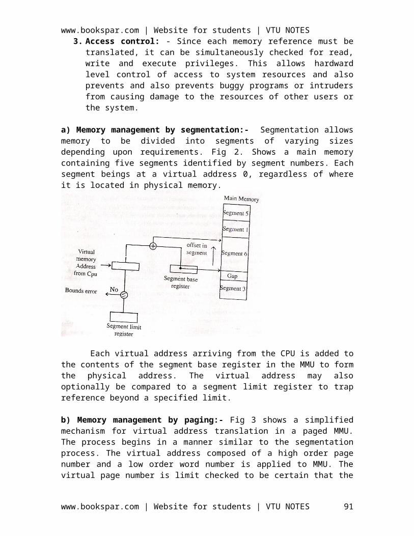
www.bookspar.com | Website for students | VTU NOTESPARALLEL PORT:-
The hardware components needed for connecting a keyboard to a processor. A typical keyboard consists of mechanical switches that are normally open. When a key is pressed, its switch closes and establishes a path for an electrical signal. This signal is detected by an encoder circuit that generates the ASCII code for the corresponding character.
Figure 11 Keyboard to processor connection.
Data Data
Address
R/
Master-ready Valid
Slave-ready
The output of the encoder consists of the bits that represent the encoded character and one control signal called Valid, which indicates that a key is being pressed. This information is sent to the interface circuit, which contains a data register, DATAIN, and a status flag, SIN. When a key is pressed, the Valid signal changes from 0 to 1, causing the ASCII code to be loaded into DATAIN and SIN to be set to 1. The status flag SIN is cleared to 0 when the processor reads the contents of the DATAIN register. The interface circuit is connected to an asynchronous bus on which transfers are controlled using the handshake signals Master-ready and Slave-ready, as indicated in figure 11. The third control line, R/ distinguishes read and write transfers.
Figure 12 shows a suitable circuit for an input interface. The output lines of the DATAIN register are connected to the data lines of the bus by means of three-state drivers, which are turned on when the processor issues a read instruction with the address that selects this register. The SIN signal is generated by a status flag circuit. This signal is also sent to the bus through a three-state driver. It is connected to bit D0, which means it will appear as bit 0 of the status register. Other bits of this register do not contain valid information. An address decoder is used to select the input interface when the high-order 31 bits of an address correspond to any of the addresses assigned to this interface. Address bit A0 determines whether the status or the data registers is to be read when the Master-ready signal is active. The control handshake is accomplished by activating the Slave-ready signal when either Read-status or Read-data is equal to 1.
www.bookspar.com | Website for students | VTU NOTES 91
ProcessorSIN
Input interface
Encoderand
Debouncingcircuit
Keyboardswitches
DATAIN

www.bookspar.com | Website for students | VTU NOTES
Fig 12 Input interface circuit
Data Data
Address
ValidR/
Master-ready Idle
Slave-ready
Fig 13 Printer to processor connection Let us now consider an output interface that can be used to connect an output
device, such as a printer, to a processor, as shown in figure 13. The printer operates under control of the handshake signals Valid and Idle in a manner similar to the handshake used on the bus with the Master-ready and Slave-ready signals. When it is ready to accept a character, the printer asserts its Idle signal. The interface circuit can then place a new character on the data lines and activate the Valid signal. In response, the printer starts printing the new character and negates the Idle signal, which in turn causes the interface to deactivate the Valid signal.
The circuit in figure 16 has separate input and output data lines for connection to an I/O device. A more flexible parallel port is created if the data lines to I/O devices are bidirectional. Figure 17 shows a general-purpose parallel interface circuit that can be
www.bookspar.com | Website for students | VTU NOTES 92
Processor SOUT
Output interface
Printer
DATAOUT

www.bookspar.com | Website for students | VTU NOTESconfigured in a variety of ways. Data lines P7 through P0 can be used for either input or output purposes. For increased flexibility, the circuit makes it possible for some lines to serve as inputs and some lines to serve as outputs, under program control. The DATAOUT register is connected to these lines via three-state drivers that are controlled by a data direction register, DDR. The processor can write any 8-bit pattern into DDR. For a given bit, if the DDR value is 1, the corresponding data line acts as an output line; otherwise, it acts as an input line.
Fig14 Output interface circuit
www.bookspar.com | Website for students | VTU NOTES 93

www.bookspar.com | Website for students | VTU NOTES
Fig 15 combined input/output interface circuit
D7 P7
D0 P0
Fig 16 A general 8-bit interfaceMy-address
www.bookspar.com | Website for students | VTU NOTES 94
DATAIN
DATAOUT
DataDirectionRegister
Registerselect

www.bookspar.com | Website for students | VTU NOTES
RS2 C1 RS1 RS0 R/W C2 Ready Accept
Fig 16 A general 8-bit parallel interface
Fig 17 A parallel port interface for the bus
Fig 18 State diagram for the timing logic.
www.bookspar.com | Website for students | VTU NOTES 95
Statusand
Control

www.bookspar.com | Website for students | VTU NOTES
Time
1 2 3
Clock
Address
R/
Data
Go
Slave-ready
Figure19 Timing for output interface
SERIAL PORT:-
A Serial port is used to connect the processor to I/O devices that require transmission of data one bit at a time. The key feature of an interface circuit for a serial port is that it is capable of communicating in a bit-serial fashion on the device side and in a bit-parallel fashion on the bus side. The transformation between the parallel and serial formats is achieved with shift registers that have parallel access capability. A block diagram of a typical serial interface is shown in figure 20. It includes the familiar DATAIN and DATAOUT registers. The input shift register accepts bit-serial input from the I/O device. When all 8 bits of data have been received, the contents of this shift register are loaded in parallel into the DATAIN register. Similarly, output data in the DATAOUT register are loaded into the output register, from which the bits are shifted out and sent to the I/O device.
Figure 20 A serial interface
Serial input
www.bookspar.com | Website for students | VTU NOTES 96
Input shift register

www.bookspar.com | Website for students | VTU NOTES
D7
D0
My-address
RS1
RS0 SerialR/ output
Ready
Accept
Receiving clock
Transmission clock
The double buffering used in the input and output paths are important. A simpler interface could be implemented by turning DATAIN and DATAOUT into shift registers and eliminating the shift registers in figure 4.37. However, this would impose awkward restrictions on the operation of the I/O device; after receiving one character from the serial line, the device cannot start receiving the next character until the processor reads the contents of DATAIN. Thus, a pause would be needed between two characters to allow the processor to read the input data. With the double buffer, the transfer of the second character can begin as soon as the first character is loaded from the shift register into the DATAIN register. Thus, provided the processor reads the contents of DATAIN before the serial transfer of the second character is completed, the interface can receive a continuous stream of serial data. An analogous situation occurs in the output path of the interface.
www.bookspar.com | Website for students | VTU NOTES 97
DATAIN
DATAOUT
Output shift register
Chip andRegister select
Statusand
Control

www.bookspar.com | Website for students | VTU NOTES Because serial interfaces play a vital role in connecting I/O devices,
several widely used standards have been developed. A standard circuit that includes the features of our example in figure 20. is known as a Universal Asynchronous Receiver Transmitter (UART). It is intended for use with low-speed serial devices. Data transmission is performed using the asynchronous start-stop format. To facilitate connection to communication links, a popular standard known as RS-232-C was developed.
STANDARD I/O INTERFACES:-
The processor bus is the bus defied by the signals on the processor chip itself. Devices that require a very high-speed connection to the processor, such as the main memory, may be connected directly to this bus. For electrical reasons, only a few devices can be connected in this manner. The motherboard usually provides another bus that can support more devices. The two buses are interconnected by a circuit, which we will call a bridge, that translates the signals and protocols of one bus into those of the other. Devices connected to the expansion bus appear to the processor as if they were connected directly to the processor’s own bus. The only difference is that the bridge circuit introduces a small delay in data transfers between the processor and those devices.
It is not possible to define a uniform standard for the processor bus. The structure of this bus is closely tied to the architecture of the processor. It is also dependent on the electrical characteristics of the processor chip, such as its clock speed. The expansion bus is not subject to these limitations, and therefore it can use a standardized signaling scheme. A number of standards have been developed. Some have evolved by default, when a particular design became commercially successful. For example, IBM developed a bus they called ISA (Industry Standard Architecture) for their personal computer known at the time as PC AT.
Some standards have been developed through industrial cooperative efforts, even among competing companies driven by their common self-interest in having compatible products. In some cases, organizations such as the IEEE (Institute of Electrical and Electronics Engineers), ANSI (American National Standards Institute), or international bodies such as ISO (International Standards Organization) have blessed these standards and given them an official status.
A given computer may use more than one bus standards. A typical Pentium computer has both a PCI bus and an ISA bus, thus providing the user with a wide range of devices to choose from.
Figure 21 An example of a computer system using different interface standards
www.bookspar.com | Website for students | VTU NOTES 98
Main Memory

www.bookspar.com | Website for students | VTU NOTESProcessor bus
PCI bus
SCSI bus
Peripheral Component Interconnect (PCI) Bus:-
The PCI bus is a good example of a system bus that grew out of the need for standardization. It supports the functions found on a processor bus bit in a standardized format that is independent of any particular processor. Devices connected to the PCI bus appear to the processor as if they were connected directly to the processor bus. They are assigned addresses in the memory address space of the processor.
The PCI follows a sequence of bus standards that were used primarily in IBM PCs. Early PCs used the 8-bit XT bus, whose signals closely mimicked those of Intel’s 80x86 processors. Later, the 16-bit bus used on the PC At computers became known as the ISA bus. Its extended 32-bit version is known as the EISA bus. Other buses developed in the eighties with similar capabilities are the Microchannel used in IBM PCs and the NuBus used in Macintosh computers.
The PCI was developed as a low-cost bus that is truly processor independent. Its design anticipated a rapidly growing demand for bus bandwidth to support high-speed disks and graphic and video devices, as well as the specialized needs of multiprocessor systems. As a result, the PCI is still popular as an industry standard almost a decade after it was first introduced in 1992.
www.bookspar.com | Website for students | VTU NOTES 99
Processor
Bridge
Additional memory
SCSIcontroller
Ethernetinterface
USBcontroller
ISAinterface
Diskcontroller
CD-ROMcontroller
Disk1 Disk 2CD-ROM
Video
Keyboard Game
IDEdisk

www.bookspar.com | Website for students | VTU NOTES
An important feature that the PCI pioneered is a plug-and-play capability for connecting I/O devices. To connect a new device, the user simply connects the device interface board to the bus. The software takes care of the rest.
Data Transfer:-
In today’s computers, most memory transfers involve a burst of data rather than just one word. The reason is that modern processors include a cache memory. Data are transferred between the cache and the main memory in burst of several words each. The words involved in such a transfer are stored at successive memory locations. When the processor (actually the cache controller) specifies an address and requests a read operation from the main memory, the memory responds by sending a sequence of data words starting at that address. Similarly, during a write operation, the processor sends a memory address followed by a sequence of data words, to be written in successive memory locations starting at the address. The PCI is designed primarily to support this mode of operation. A read or write operation involving a single word is simply treated as a burst of length one.
The bus supports three independent address spaces: memory, I/O, and configuration. The first two are self-explanatory. The I/O address space is intended for use with processors, such as Pentium, that have a separate I/O address space. However, as noted , the system designer may choose to use memory-mapped I/O even when a separate I/O address space is available. In fact, this is the approach recommended by the PCI its plug-and-play capability. A 4-bit command that accompanies the address identifies which of the three spaces is being used in a given data transfer operation.
The signaling convention on the PCI bus is similar to the one used, we assumed that the master maintains the address information on the bus until data transfer is completed. But, this is not necessary. The address is needed only long enough for the slave to be selected. The slave can store the address in its internal buffer. Thus, the address is needed on the bus for one clock cycle only, freeing the address lines to be used for sending data in subsequent clock cycles. The result is a significant cost reduction because the number of wires on a bus is an important cost factor. This approach in used in the PCI bus.
Figure 22 Use of a PCI bus in a computer system.
www.bookspar.com | Website for students | VTU NOTES 100
PCI bridgeMain
memory

www.bookspar.com | Website for students | VTU NOTES
PCI bus
At any given time, one device is the bus master. It has the right to initiate data transfers by issuing read and write commands. A master is called an initiator in PCI terminology. This is either a processor or a DMA controller. The addressed device that responds to read and write commands is called a target.
Device Configuration:-
When an I/O device is connected to a computer, several actions are needed to configure both the device and the software that communicates with it.
The PCI simplifies this process by incorporating in each I/O device interface a small configuration ROM memory that stores information about that device. The configuration ROMs of all devices is accessible in the configuration address space. The PCI initialization software reads these ROMs whenever the system is powered up or reset. In each case, it determines whether the device is a printer, a keyboard, an Ethernet interface, or a disk controller. It can further learn bout various device options and characteristics.
Devices are assigned addresses during the initialization process. This means that during the bus configuration operation, devices cannot be accessed based on their address, as they have not yet been assigned one. Hence, the configuration address space uses a different mechanism. Each device has an input signal called Initialization Device Select, IDSEL#.
The PCI bus has gained great popularity in the PC word. It is also used in many other computers, such as SUNs, to benefit from the wide range of I/O devices for which a PCI interface is available. In the case of some processors, such as the Compaq Alpha, the PCI-processor bridge circuit is built on the processor chip itself, further simplifying system design and packaging.
SCSI Bus:-
The acronym SCSI stands for Small Computer System Interface. It refers to a standard bus defined by the American National Standards Institute (ANSI) under the designation X3.131 . In the original specifications of the standard, devices such as disks are connected to a computer via a 50-wire cable, which can be up to 25 meters in length and can transfer data at rates up to 5 megabytes/s.
www.bookspar.com | Website for students | VTU NOTES 101
Host
Disk PrinterEthernet interface

www.bookspar.com | Website for students | VTU NOTES The SCSI bus standard has undergone many revisions, and its data transfer
capability has increased very rapidly, almost doubling every two years. SCSI-2 and SCSI-3 have been defined, and each has several options. A SCSI bus may have eight data lines, in which case it is called a narrow bus and transfers data one byte at a time. Alternatively, a wide SCSI bus has 16 data lines and transfers data 16 bits at a time. There are also several options for the electrical signaling scheme used.
Devices connected to the SCSI bus are not part of the address space of the processor in the same way as devices connected to the processor bus. The SCSI bus is connected to the processor bus through a SCSI controller. This controller uses DMA to transfer data packets from the main memory to the device, or vice versa. A packet may contain a block of data, commands from the processor to the device, or status information about the device.
To illustrate the operation of the SCSI bus, let us consider how it may be used with a disk drive. Communication with a disk drive differs substantially from communication with the main memory.
A controller connected to a SCSI bus is one of two types – an initiator or a target. An initiator has the ability to select a particular target and to send commands specifying the operations to be performed. Clearly, the controller on the processor side, such as the SCSI controller, must be able to operate as an initiator. The disk controller operates as a target. It carries out the commands it receives from the initiator. The initiator establishes a logical connection with the intended target. Once this connection has been established, it can be suspended and restored as needed to transfer commands and bursts of data. While a particular connection is suspended, other device can use the bus to transfer information. This ability to overlap data transfer requests is one of the key features of the SCSI bus that leads to its high performance.
Data transfers on the SCSI bus are always controlled by the target controller. To send a command to a target, an initiator requests control of the bus and, after winning arbitration, selects the controller it wants to communicate with and hands control of the bus over to it. Then the controller starts a data transfer operation to receive a command from the initiator.
The processor sends a command to the SCSI controller, which causes the following sequence of event to take place:
1. The SCSI controller, acting as an initiator, contends for control of the bus.2. When the initiator wins the arbitration process, it selects the target controller and
hands over control of the bus to it.3. The target starts an output operation (from initiator to target); in response to this,
the initiator sends a command specifying the required read operation.4. The target, realizing that it first needs to perform a disk seek operation, sends a
message to the initiator indicating that it will temporarily suspend the connection between them. Then it releases the bus.
5. The target controller sends a command to the disk drive to move the read head to the first sector involved in the requested read operation. Then, it reads the data
www.bookspar.com | Website for students | VTU NOTES 102

www.bookspar.com | Website for students | VTU NOTESstored in that sector and stores them in a data buffer. When it is ready to begin transferring data to the initiator, the target requests control of the bus. After it wins arbitration, it reselects the initiator controller, thus restoring the suspended connection.
6. The target transfers the contents of the data buffer to the initiator and then suspends the connection again. Data are transferred either 8 or 16 bits in parallel, depending on the width of the bus.
7. The target controller sends a command to the disk drive to perform another seek operation. Then, it transfers the contents of the second disk sector to the initiator as before. At the end of this transfers, the logical connection between the two controllers is terminated.
8. As the initiator controller receives the data, it stores them into the main memory using the DMA approach.
9. The SCSI controller sends as interrupt to the processor to inform it that the requested operation has been completed
This scenario show that the messages exchanged over the SCSI bus are at a higher level than those exchanged over the processor bus. In this context, a “higher level” means that the messages refer to operations that may require several steps to complete, depending on the device. Neither the processor nor the SCSI controller need be aware of the details of operation of the particular device involved in a data transfer. In the preceding example, the processor need not be involved in the disk seek operation.
UNIVERSAL SERIAL BUS (USB):-
The synergy between computers and communication is at the heart of today’s information technology revolution. A modern computer system is likely to involve a wide variety of devices such as keyboards, microphones, cameras, speakers, and display devices. Most computers also have a wired or wireless connection to the Internet. A key requirement is such an environment is the availability of a simple, low-cost mechanism to connect these devices to the computer, and an important recent development in this regard is the introduction of the Universal Serial Bus (USB). This is an industry standard developed through a collaborative effort of several computer and communication companies, including Compaq, Hewlett-Packard, Intel, Lucent, Microsoft, Nortel Networks, and Philips.
The USB supports two speeds of operation, called low-speed (1.5 megabits/s) and full-speed (12 megabits/s). The most recent revision of the bus specification (USB 2.0) introduced a third speed of operation, called high-speed (480 megabits/s). The USB is quickly gaining acceptance in the market place, and with the addition of the high-speed capability it may well become the interconnection method of choice for most computer devices.
The USB has been designed to meet several key objectives: Provides a simple, low-cost and easy to use interconnection system that
overcomes the difficulties due to the limited number of I/O ports available on a computer.
www.bookspar.com | Website for students | VTU NOTES 103
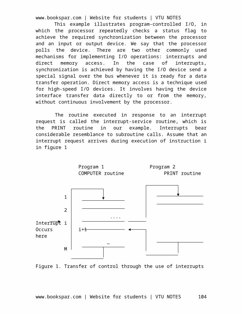
www.bookspar.com | Website for students | VTU NOTES Accommodate a wide range of data transfer characteristics for I/O devices,
including telephone and Internet connections. Enhance user convenience through a “plug-and-play” mode of operation
Port Limitation:-
The parallel and serial ports described in previous section provide a general-purpose point of connection through which a variety of low-to medium-speed devices can be connected to a computer. For practical reasons, only a few such ports are provided in a typical computer.
Device Characteristics:-
The kinds of devices that may be connected to a computer cover a wide range of functionality. The speed, volume, and timing constraints associated with data transfers to and from such devices vary significantly.
A variety of simple devices that may be attached to a computer generate data of a similar nature – low speed and asynchronous. Computer mice and the controls and manipulators used with video games are good examples.
Plug-and-Play:-
As computers become part of everyday life, their existence should become increasingly transparent. For example, when operating a home theater system, which includes at least one computer, the user should not find it necessary to turn the computer off or to restart the system to connect or disconnect a device.
The plug-and-play feature means that a new device, such as an additional speaker, can be connected at any time while the system is operating. The system should detect the existence of this new device automatically, identify the appropriate device-driver software and any other facilities needed to service that device, and establish the appropriate addresses and logical connections to enable them to communicate.
The plug-and-play requirement has many implications at all levels in the system, from the hardware to the operating system and the applications software. One of the primary objectives of the design of the USB has been to provide a plug-and-play capability.
USB Architecture:-
The discussion above points to the need for an interconnection system that combines low cost, flexibility, and high data-transfer bandwidth. Also, I/O devices may be located at some distance from the computer to which they are connected. The requirement for high bandwidth would normally suggest a wide bus that carries 8, 16, or more bits in parallel. However, a large number of wires increases cost and complexity and is inconvenient to the user. Also, it is difficult to design a wide bus that carries data
www.bookspar.com | Website for students | VTU NOTES 104

www.bookspar.com | Website for students | VTU NOTESfor a long distance because of the data skew problem discussed. The amount of skew increases with distance and limits the data that can be used.
A serial transmission format has been chosen for the USB because a serial bus satisfies the low-cost and flexibility requirements. Clock and data information are encoded together and transmitted as a single signal. Hence, there are no limitations on clock frequency or distance arising from data skew. Therefore, it is possible to provide a high data transfer bandwidth by using a high clock frequency. As pointed out earlier, the USB offers three bit rates, ranging from 1.5 to 480 megabits/s, to suit the needs of different I/O devices.
Figure 23 Universal Serial Bus tree structure.
To accommodate a large number of devices that can be added or removed at any time, the USB has the tree structure shown in figure 23. Each node of the tree has a device called a hub, which acts as an intermediate control point between the host and the I/O devices. At the root of the tree, a root hub connects the entire tree to the host computer. The leaves of the tree are the I/O devices being served (for example, keyboard, Internet connection, speaker, or digital TV), which are called functions in USB terminology. For consistency with the rest of the discussion in the book, we will refer to these devices as I/O devices.
The tree structure enables many devices to be connected while using only simple point-to-point serial links. Each hub has a number of ports where devices may be connected, including other hubs. In normal operation, a hub copies a message that it receives from its upstream connection to all its downstream ports. As a result, a message sent by the host computer is broadcast to all I/O devices, but only the addressed device will respond to that message. In this respect, the USB functions in the same way as the bus in figure 4.1. However, unlike the bus in figure 4.1, a message from an I/O device is sent only upstream towards the root of the tree and is not seen by other devices. Hence, the USB enables the host to communicate with the I/O devices, but it does not enable these devices to communicate with each other.
www.bookspar.com | Website for students | VTU NOTES 105
Host computer
Roothub
Hub Hub
Hub
I/Odevice
I/Odevice
I/Odevice
I/Odevice
I/Odevice
I/Odevice

www.bookspar.com | Website for students | VTU NOTES Note how the tree structure helps meet the USB’s design objectives. The tree
makes it possible to connect a large number of devices to a computer through a few ports (the root hub). At the same time, each I/O device is connected through a serial point-to-point connection. This is an important consideration in facilitating the plug-and-play feature, as we will see shortly.
The USB operates strictly on the basis of polling. A device may send a message only in response to a poll message from the host. Hence, upstream messages do not encounter conflicts or interfere with each other, as no two devices can send messages at the same time. This restriction allows hubs to be simple, low-cost devices.
The mode of operation described above is observed for all devices operating at either low speed or full speed. However, one exception has been necessitated by the introduction of high-speed operation in USB version 2.0. Consider the situation in figure 24. Hub A is connected to the root hub by a high-speed link. This hub serves one high-speed device, C, and one low-speed device, D. Normally, a messages to device D would be sent at low speed from the root hub. At 1.5 megabits/s, even a short message takes several tens of microsends. For the duration of this message, no other data transfers can take place, thus reducing the effectiveness of the high-speed links and introducing unacceptable delays for high-speed devices. To mitigate this problem, the USB protocol requires that a message transmitted on a high-speed link is always transmitted at high speed, even when the ultimate receiver is a low-speed device. Hence, a message at low speed to device D. The latter transfer will take a long time, during which high-speed traffic to other nodes is allowed to continue. For example, the root hub may exchange several message with device C while the low-speed message is being sent from hub A to device D. During this period, the bus is said to be split between high-speed and low-speed traffic. The message to device D is preceded and followed by special commands to hub A to start and end the split-traffic mode of operation, respectively.
Figure 24 Split bus operation
HS – High speedF/LS – Full/Low speed
The USB standard specifies the hardware details of USB interconnections as well as the organization and requirements of the host software. The purpose of the USB
www.bookspar.com | Website for students | VTU NOTES 106
Host computer
Root Hub
Hub
AHub
B
DeviceC
Device D
HS HS
HS F/LS

www.bookspar.com | Website for students | VTU NOTESsoftware is to provide bidirectional communication links between application software and I/O devices. These links are called pipes. Any data entering at one end of a pipe is delivered at the other end. Issues such as addressing, timing, or error detection and recovery are handled by the USB protocols.
Addressing:-
In earlier discussions of input and output operations, we explained that I/O devices are normally identified by assigning them a unique memory address. In fact, a device usually has several addressable locations to enable the software to send and receive control and status information and to transfer data.
When a USB is connected to a host computer, its root hub is attached to the processor bus, where it appears as a single device. The host software communicates with individual devices attached to the USB by sending packets of informations, which the root hub forwards to the appropriate device in the USB tree.
Each device on the USB, whether it is a hub or an I/O device, is assigned a 7-bit address. This address is local to the USB tree and is not related in any way to the addresses used on the processor bus. A hub may have any number of devices or other hubs connected to it, and addresses are assigned arbitrarily. When a device is first connected to a hub, or when it is powered on, it has the address 0. The hardware of the hub to which this device is connected is capable of detecting that the device has been connected, and it records this fact as part of its own status information. Periodically, the host polls each hub to collect status information and learn about new devices that may have been added or disconnected. When the host is informed that a new device has been connected, it uses a sequence of commands to send a reset signal on the corresponding hub port, read information from the device about its capabilities, send configuration information to the device, and assign the device a unique USB address. Once this sequence is completed the device begins normal operation and responds only to the new address.
When a device is powered off, a similar procedure is followed. The corresponding hub reports this fact to the USB system software, which in turn updates its tables. Of course, if the device that has been disconnected is itself a hub, all devices connected through that hub must also be recorded as disconnected. The USB software must maintain a complete picture of the bus topology and the connected devices at all times.
USB Protocols:-
All information transferred over the USB is organized in packets, where a packet consists of one or more bytes of information. There are many types of packets that perform a variety of control functions. We illustrate the operation of the USB by giving a few examples of the key packet types and show how they are used.
The information transferred on the USB can be divided into two broad categories: control and data. Control packets perform such tasks as addressing a device to
www.bookspar.com | Website for students | VTU NOTES 107

www.bookspar.com | Website for students | VTU NOTESinitiate data transfer, acknowledging that data have been received correctly, or indicating an error. Data packets carry information that is delivered to a device. For example, input and output data are transferred inside data packets.
A packet consists of one or more fields containing different kinds of information. The first field of any packet is called the packet identifier, PID, which identifies the type of that packet. There are four bits of information in this field, but they are transmitted twice. The first time they are sent with their true values, and the second time with each bit complemented, as shown in figure 4.45a. This enables the receiving device to verify that the PID byte has been received correctly.
The four PID bits identify one of 16 different packet types. Some control packets, such as ACK (Acknowledge), consist only of the PID byte. Control packets used for controlling data transfer operations are called toke packets. They have the format shown in figure 4.45b. A token packet starts with the PID field, using one of two PID values to distinguish between an IN packet and an OUT packet, which control input and output transfers, respectively. The PID field is followed by the 7-bit address of a device and the 4-bit endpoint number within that device. The packet ends with 5 bits for error checking, using a method called cyclic redundancy check (CRC). The CRC bits are computed based on the contents of the address and endpoint fields. By performing an inverse computation, the receiving device can determine whether the packet has been received correctly.
Data packets, which carry input and output data, have the format shown in figure. The packet identifier field is followed by up to 8192 bits of data, then 16 error-checking bits. Three different PID patterns are used to identify data packets, so that data packets may be numbered 0,1, or 2. Note that data packets do not carry a device address or an endpoint number. This information is included in the IN or OUT token packet that initiates the transfer.
Successive data packets on a full-speed or low-speed pipe carry the numbers 0 and 1, alternately. This simplifies recovery from transmission errors. If a token, data, or acknowledgement packet is lost as a result of a transmission error, the sender resends the entire sequence. By checking the data packet number in the PID field, the receiver can detect and discard duplicate packets. High-speed data packets are sequentially numbered 0, 1, 2, 0, and so on.
A) packet identifier Field
B) Token Packet ,IN or OUT
8 0 TO 8192 16
www.bookspar.com | Website for students | VTU NOTES 108
PID3PID1 PID2PID0PID3PID2PID1PID0
PID ADDR ENDP CRC16

www.bookspar.com | Website for students | VTU NOTES
C) Data Packet
Figure 24 USB Packet formats
Host Hub I/O Device
Token
Data0Time
ACK
Token
Data0
ACK
Token
Data1
ACK
Token
Data1
ACK
www.bookspar.com | Website for students | VTU NOTES 109
PID DATA CRC16

www.bookspar.com | Website for students | VTU NOTESFig 27 An output transfer
Input operations follow a similar procedure. The host sends a token packet of type IN containing the device address. In effect, this packet is a poll asking the device to send any input data it may have. The device responds by sending a data packet followed by an ACK. If it has no data ready, it responds by sending a negative acknowledgement (NAK) instead.
We pointed out that a bus that has a mix of full/low-speed links and high-speed links uses the split-traffic mode of operation in order not to delay messages on high-speed links. In such cases, an IN or an OUT packet intended for a full-or-low-speed device is preceded by a special control packet that starts the split-traffic mode.
Isochronous Traffic on USB:-
One of the key objectives of the USB is to support the transfer of isochronous data, such as sampled voice, in a simple manner. Devices that generates or receives isochronous data require a time reference to control the sampling process. To provide this reference. Transmission over the USB is divided into frames of equal length. A frame is 1ms long for low-and full-speed data. The root hub generates a Start of Frame control packet (SOF) precisely once every 1 ms to mark the beginning of a new frame.
The arrival of an SOF packet at any device constitutes a regular clock signal that the device can use for its own purposes. To assist devices that may need longer periods of time, the SOF packet carries an 11-bit frame number, as shown. Following each SOF packet, the host carries out input and output transfers for isochronous devices. This means that each device will have an opportunity for an input or output transfer once every 1 ms.
Electrical Characteristics:-
The cables used for USB connections consist of four wires. Two are used to carry power, +5V and Ground. Thus, a hub or an I/O device may be powered directly from the bus, or it may have its own external power connection. The other two wires are used to carry data. Different signaling schemes are used for different speeds of transmission. At low speed, 1s and 0s are transmitted by sending a high voltage state (5V) on one or the other o the two signal wires. For high-speed links, differential transmission is used.
************************
www.bookspar.com | Website for students | VTU NOTES 110